Embed Size (px)
Citation preview
Development of Readout ASIC
for FPCCD Vertex Detector
Tomoyuki Saito (Tohoku University)
1
ALCPG – Linear Collider Workshop of the America
21 March, 2011. Eugene, USA
Y. Sugimoto, A. Miyamoto, Y. Takubo (KEK)
H. Ikeda (JAXA), H. Sato (Shinsyu)
K. Itagaki, H. Yamamoto (Tohoku)
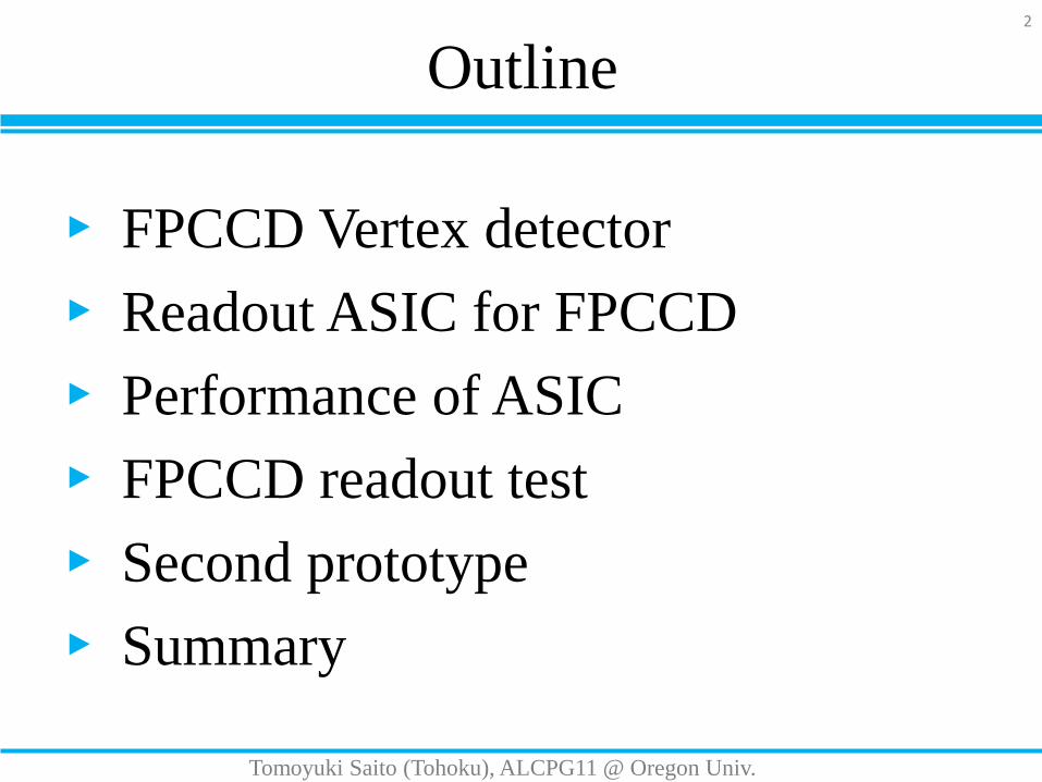
Outline
► FPCCD Vertex detector
► Readout ASIC for FPCCD
► Performance of ASIC
► FPCCD readout test
► Second prototype
► Summary
2
Tomoyuki Saito (Tohoku), ALCPG11 @ Oregon Univ.
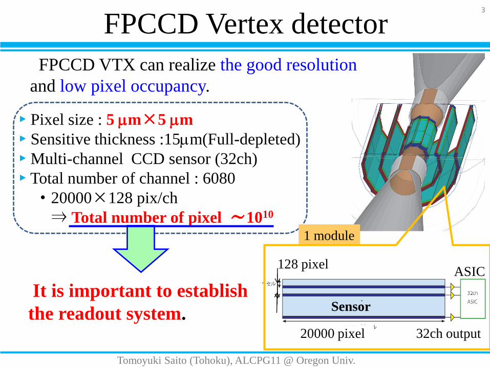
FPCCD VTX can realize the good resolution
and low pixel occupancy.
FPCCD Vertex detector3
32ch output
1 module
Sensor
ASIC
20000 pixel
128 pixel
► Pixel size : 5 mm×5 mm
► Sensitive thickness :15mm(Full-depleted)
► Multi-channel CCD sensor (32ch)
► Total number of channel : 6080
・20000×128 pix/ch
⇒ Total number of pixel ~1010
Tomoyuki Saito (Tohoku), ALCPG11 @ Oregon Univ.
It is important to establish
the readout system.
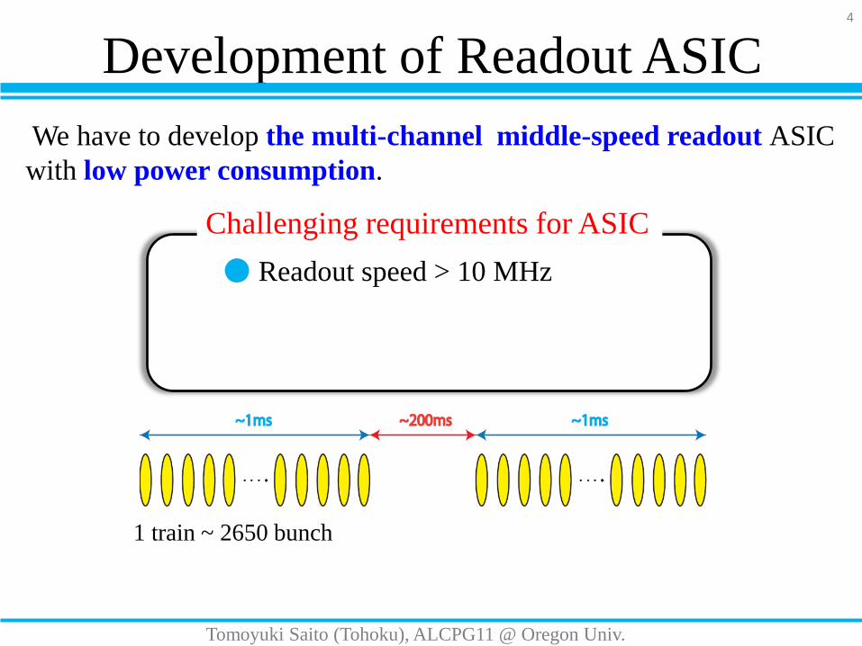
Development of Readout ASIC
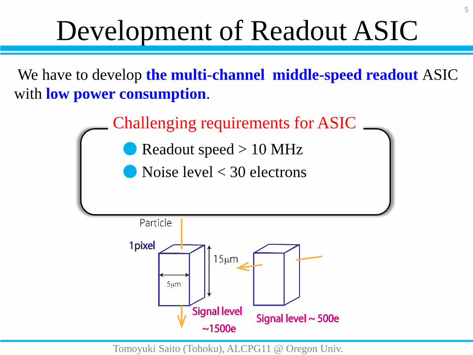
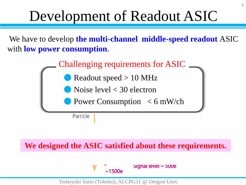
We have to develop the multi-channel middle-speed readout ASIC
with low power consumption.
4
Tomoyuki Saito (Tohoku), ALCPG11 @ Oregon Univ.
● Readout speed > 10 MHz
Challenging requirements for ASIC
1 train ~ 2650 bunch
Development of Readout ASIC5
Tomoyuki Saito (Tohoku), ALCPG11 @ Oregon Univ.
● Readout speed > 10 MHz
● Noise level < 30 electrons
Challenging requirements for ASIC
We have to develop the multi-channel middle-speed readout ASIC
with low power consumption.
Development of Readout ASIC6
● Readout speed > 10 MHz
● Noise level < 30 electron
● Power Consumption < 6 mW/ch
Challenging requirements for ASIC
Tomoyuki Saito (Tohoku), ALCPG11 @ Oregon Univ.
We have to develop the multi-channel middle-speed readout ASIC
with low power consumption.
We designed the ASIC satisfied about these requirements.
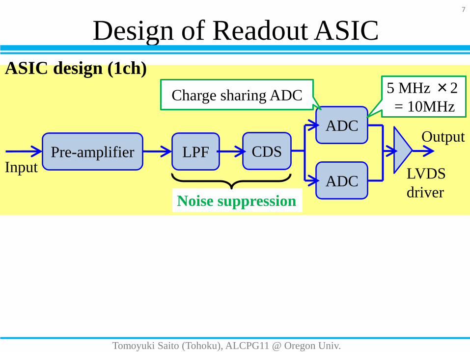
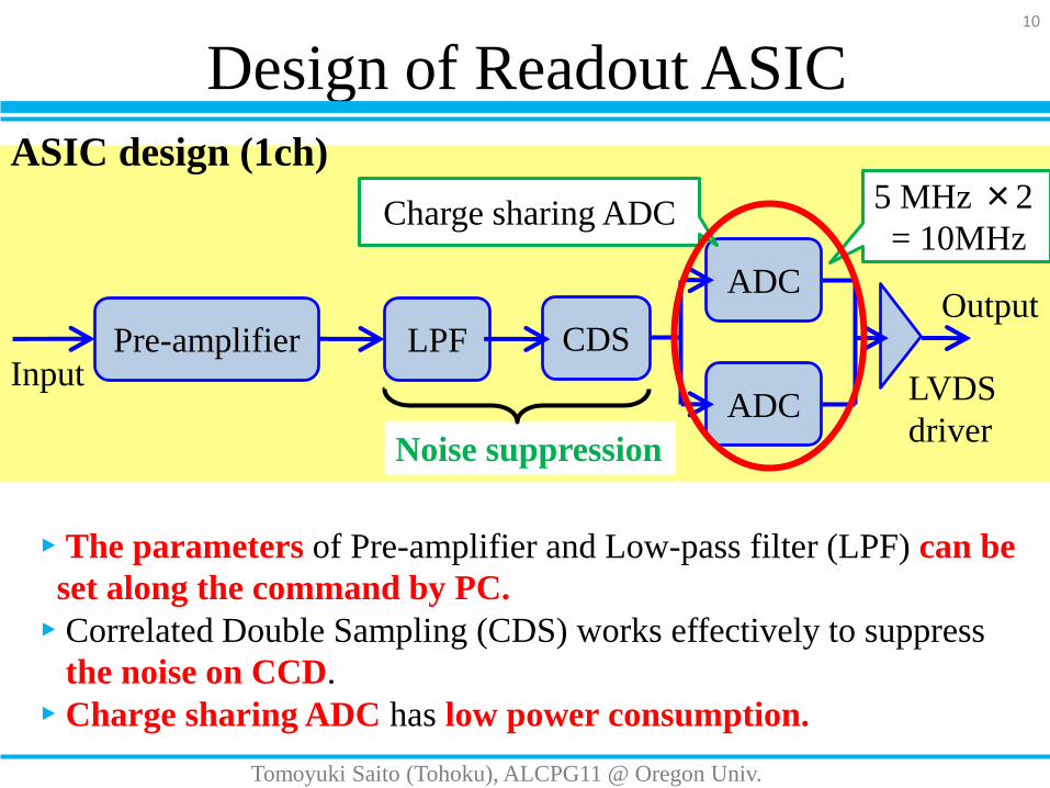
Design of Readout ASIC
Pre-amplifier LPF CDS
ADC
ADCLVDS
driver
Output
Input
Charge sharing ADC
ASIC design (1ch)
7
Noise suppression
5 MHz ×2
= 10MHz
Tomoyuki Saito (Tohoku), ALCPG11 @ Oregon Univ.
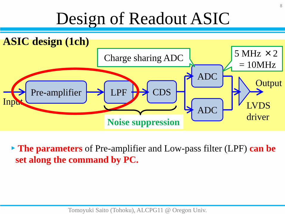
Design of Readout ASIC
Pre-amplifier LPF CDS
ADC
ADCLVDS
driver
Output
Input
Charge sharing ADC5 MHz ×2
= 10MHz
Noise suppression
ASIC design (1ch)
8
▸ The parameters of Pre-amplifier and Low-pass filter (LPF) can be
set along the command by PC.
Tomoyuki Saito (Tohoku), ALCPG11 @ Oregon Univ.
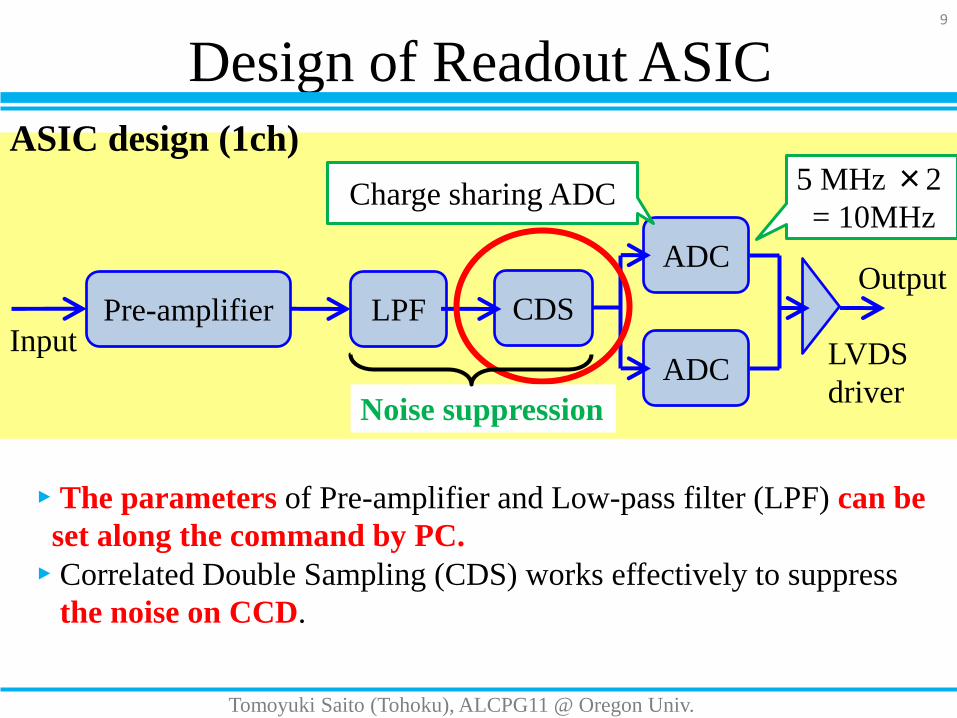
Design of Readout ASIC
Pre-amplifier LPF CDS
ADC
ADCLVDS
driver
Output
Input
Charge sharing ADC5 MHz ×2
= 10MHz
ASIC design (1ch)
▸ The parameters of Pre-amplifier and Low-pass filter (LPF) can be
set along the command by PC.
▸ Correlated Double Sampling (CDS) works effectively to suppress
the noise on CCD.
9
Noise suppression
Tomoyuki Saito (Tohoku), ALCPG11 @ Oregon Univ.
Design of Readout ASIC
Pre-amplifier LPF CDS
ADC
ADCLVDS
driver
Output
Input
Charge sharing ADC5 MHz ×2
= 10MHz
ASIC design (1ch)
▸ The parameters of Pre-amplifier and Low-pass filter (LPF) can be
set along the command by PC.
▸ Correlated Double Sampling (CDS) works effectively to suppress
the noise on CCD.
▸ Charge sharing ADC has low power consumption.
10
Noise suppression
Tomoyuki Saito (Tohoku), ALCPG11 @ Oregon Univ.
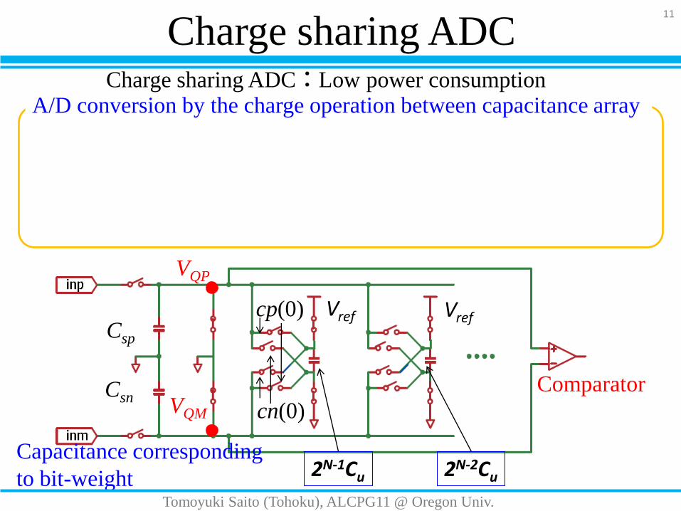
cp(0)
VQP
VQM
Vref Vref
Comparator
Csp
Csn
Capacitance corresponding
to bit-weight
cn(0)
A/D conversion by the charge operation between capacitance array
2N-1Cu 2N-2Cu
Tomoyuki Saito (Tohoku), ALCPG11 @ Oregon Univ.
Charge sharing ADC11
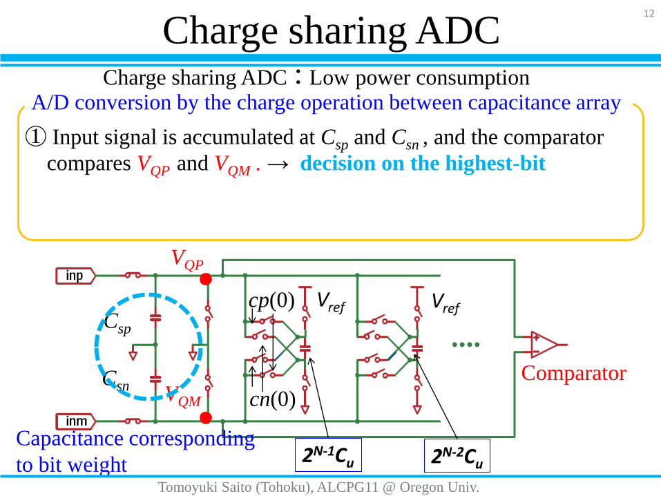
Charge sharing ADC:Low power consumption
cp(0)
VQP
VQM
Vref Vref
Comparator
Csp
Csn
Capacitance corresponding
to bit weight
cn(0)
Charge sharing ADC
① Input signal is accumulated at Csp and Csn , and the comparator
compares VQP and VQM . → decision on the highest-bit
A/D conversion by the charge operation between capacitance array
12
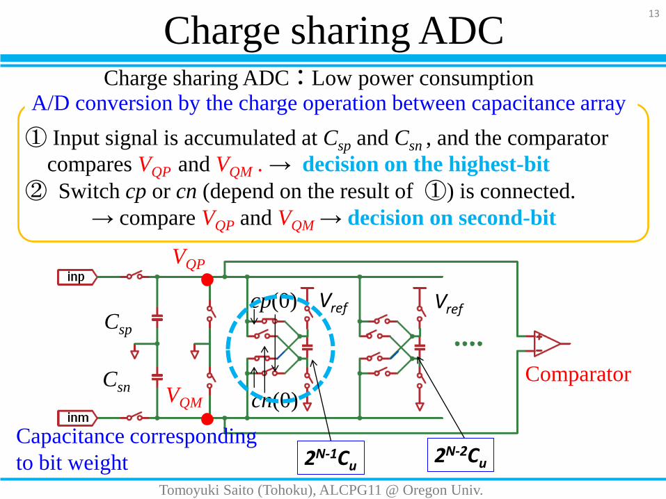
Charge sharing ADC:Low power consumption
2N-2Cu
Tomoyuki Saito (Tohoku), ALCPG11 @ Oregon Univ.
2N-1Cu
cp(0)
VQP
VQM
Vref Vref
Comparator
Csp
Csn
2N-2Cu
Capacitance corresponding
to bit weight
cn(0)
Charge sharing ADC
① Input signal is accumulated at Csp and Csn , and the comparator
compares VQP and VQM . → decision on the highest-bit
② Switch cp or cn (depend on the result of ①) is connected.
→ compare VQP and VQM → decision on second-bit
A/D conversion by the charge operation between capacitance array
13
Charge sharing ADC:Low power consumption
Tomoyuki Saito (Tohoku), ALCPG11 @ Oregon Univ.
2N-1Cu
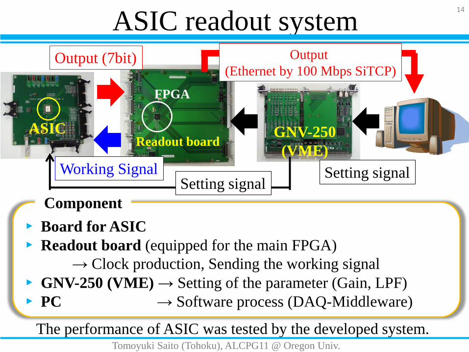
ASIC readout system
ASICReadout board
Working SignalSetting signal
Setting signal
► Board for ASIC
► Readout board (equipped for the main FPGA)
→ Clock production, Sending the working signal
► GNV-250 (VME) → Setting of the parameter (Gain, LPF)
► PC → Software process (DAQ-Middleware)
Component
Output
(Ethernet by 100 Mbps SiTCP)
14
GNV-250
(VME)
Output (7bit)
The performance of ASIC was tested by the developed system.
FPGA
Tomoyuki Saito (Tohoku), ALCPG11 @ Oregon Univ.
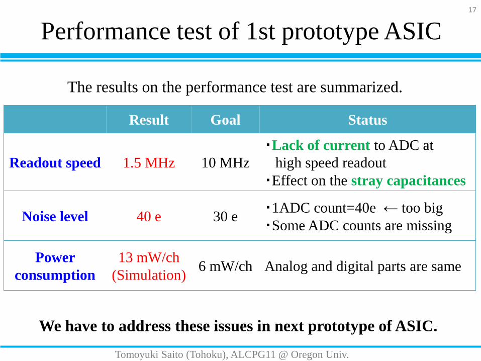
Performance test of 1st prototype ASIC
The results on the performance test are summarized.
15
Tomoyuki Saito (Tohoku), ALCPG11 @ Oregon Univ.
Result Goal Status
Readout speed 1.5 MHz 10 MHz
・Lack of current to ADC at
high speed readout
・Effect on the stray capacitances
Noise level 40 e 30 e・1ADC count=40e ← too big
・Some ADC counts are missing
Power
consumption
13 mW/ch
(Simulation)6 mW/ch Analog and digital parts are same
Result Goal Status
Readout speed 1.5 MHz 10 MHz
・Lack of current to ADC at
high speed readout
・Effect on the stray capacitances
Noise level 40 e 30 e・1ADC count=40e ← too big
・Some ADC counts are missing
Power
consumption
13 mW/ch
(Simulation)6 mW/ch Analog and digital parts are same
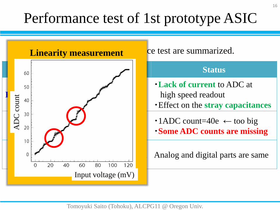
Performance test of 1st prototype ASIC
The results on the performance test are summarized.
16
Tomoyuki Saito (Tohoku), ALCPG11 @ Oregon Univ.
Linearity measurement
Input voltage (mV)
AD
C c
ou
nt
Performance test of 1st prototype ASIC
Result Goal Status
Readout speed 1.5 MHz 10 MHz
・Lack of current to ADC at
high speed readout
・Effect on the stray capacitances
Noise level 40 e 30 e・1ADC count=40e ← too big
・Some ADC counts are missing
Power
consumption
13 mW/ch
(Simulation)6 mW/ch Analog and digital parts are same
The results on the performance test are summarized.
17
We have to address these issues in next prototype of ASIC.
Tomoyuki Saito (Tohoku), ALCPG11 @ Oregon Univ.
FPCCD readout
Tomoyuki Saito (Tohoku), ALCPG11 @ Oregon Univ.
FPCCD readout system
ASIC
The readout test of FPCCD was performed by the developed system.
FPCCD prototype (by Hamamatsu)
► Pixel size : 12 mm×12 mm
► Number of channel : 4
19
Readout board
Working Signal
Setting signal
Setting signal
Output (Ethernet by 100Mbps SiTCP)
GNV-250
(VME)
Output (7bit)
Tomoyuki Saito (Tohoku), ALCPG11 @ Oregon Univ.
FPCCD readout test
The signal which was sent from FPCCD to the PC is investigates.
20
Pedestal distribution (ADC count)
⇒ Uniform
distribution
Tomoyuki Saito (Tohoku), ALCPG11 @ Oregon Univ.
FPCCD readout test
Pedestal distribution (ADC count)
Photomask
The developed readout system works normally.
LED irradiation test
Success in reading “ILC”
⇒ Uniform
distribution
21
Tomoyuki Saito (Tohoku), ALCPG11 @ Oregon Univ.
The signal which was sent from FPCCD to the PC is investigates.
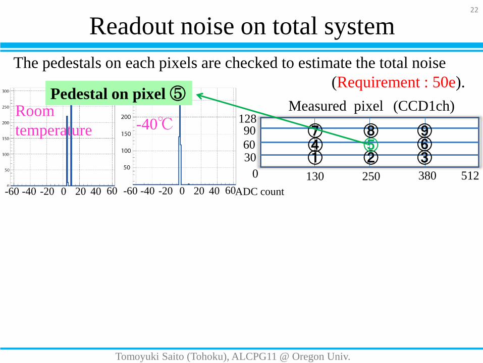
Readout noise on total system
Room
temperature -40℃
512250
60
0
30
90128
130 380
① ② ③④ ⑤ ⑥⑦ ⑧ ⑨
0 60-60 20-20 40-40 0 60-60 20-20 40-40 ADC count
22
Measured pixel (CCD1ch)
Tomoyuki Saito (Tohoku), ALCPG11 @ Oregon Univ.
The pedestals on each pixels are checked to estimate the total noise
(Requirement : 50e).Pedestal on pixel ⑤
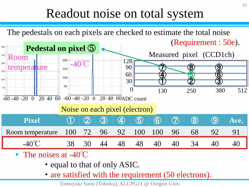
Readout noise on total system
The pedestals on each pixels are checked to estimate the total noise
(Requirement : 50e).
Room
temperature -40℃
512250
60
0
30
90128
130 380
① ② ③④ ⑤ ⑥⑦ ⑧ ⑨
Measured pixel (CCD1ch)
Pixel ① ② ③ ④ ⑤ ⑥ ⑦ ⑧ ⑨ Ave.
Room temperature 100 72 96 92 100 100 96 68 92 91
-40℃ 38 30 44 48 48 40 40 34 40 40
0 60-60 20-20 40-40 0 60-60 20-20 40-40
Pedestal on pixel ⑤
Noise on each pixel (electron)
► The noises at -40℃・ equal to that of only ASIC.
・ are satisfied with the requirement (50 electrons).
ADC count
23
Tomoyuki Saito (Tohoku), ALCPG11 @ Oregon Univ.
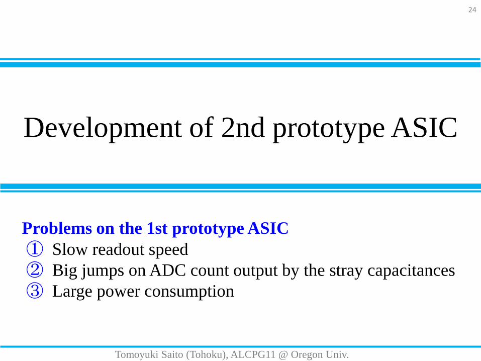
Development of 2nd prototype ASIC
24
Problems on the 1st prototype ASIC
① Slow readout speed
② Big jumps on ADC count output by the stray capacitances
③ Large power consumption
Tomoyuki Saito (Tohoku), ALCPG11 @ Oregon Univ.
Development of 2nd prototype ASIC25
Goal : 10 MHz readout speed and solution to ADC count jumps
Tomoyuki Saito (Tohoku), ALCPG11 @ Oregon Univ.
Development of 2nd prototype ASIC26
Main modification
● Readout speed : The number of pins is increased, 80 → 100.
Tomoyuki Saito (Tohoku), ALCPG11 @ Oregon Univ.
Goal : 10 MHz readout speed and solution to ADC count jumps
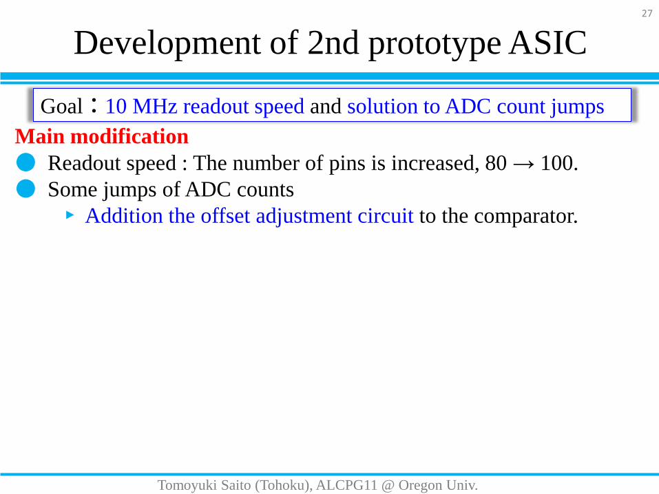
Development of 2nd prototype ASIC27
Main modification
● Readout speed : The number of pins is increased, 80 → 100.
● Some jumps of ADC counts
► Addition the offset adjustment circuit to the comparator.
Tomoyuki Saito (Tohoku), ALCPG11 @ Oregon Univ.
Goal : 10 MHz readout speed and solution to ADC count jumps
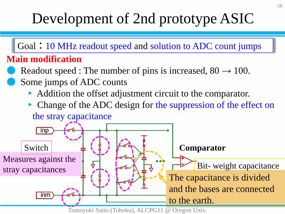
Development of 2nd prototype ASIC28
The capacitance is divided
and the bases are connected
to the earth.
Measures against the
stray capacitances
Comparator
Main modification
● Readout speed : The number of pins is increased, 80 → 100.
● Some jumps of ADC counts
► Addition the offset adjustment circuit to the comparator.
► Change of the ADC design for the suppression of the effect on
the stray capacitance
Switch
Bit- weight capacitance
Tomoyuki Saito (Tohoku), ALCPG11 @ Oregon Univ.
Goal : 10 MHz readout speed and solution to ADC count jumps
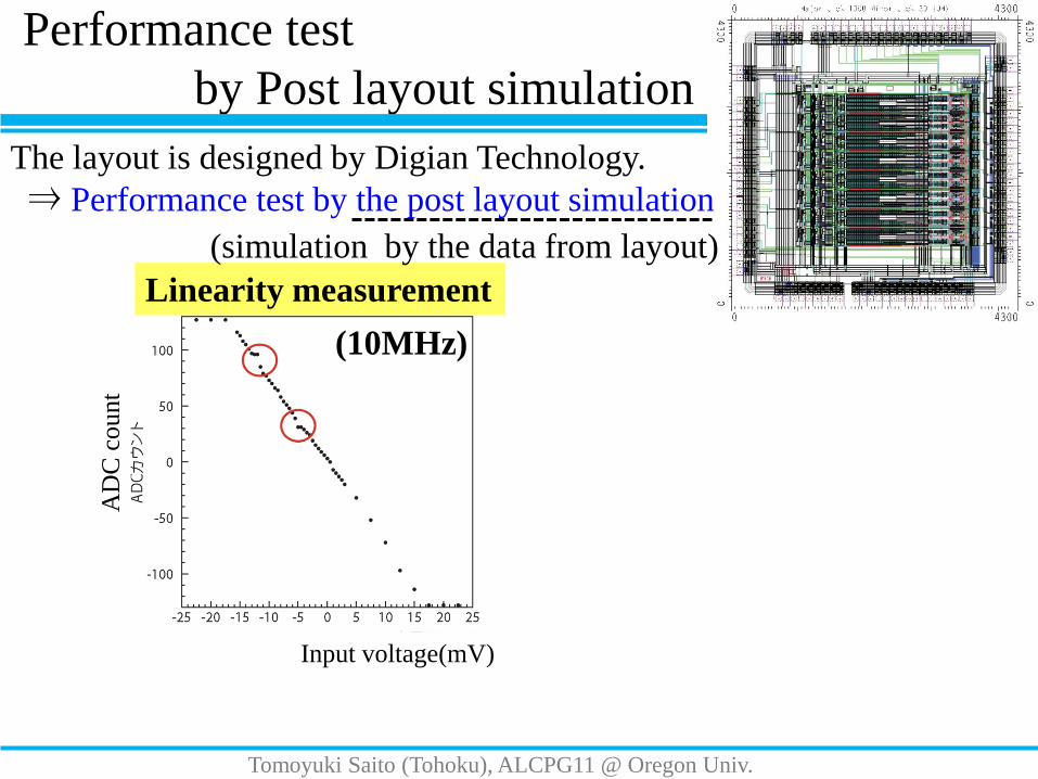
Performance test
by Post layout simulation
29
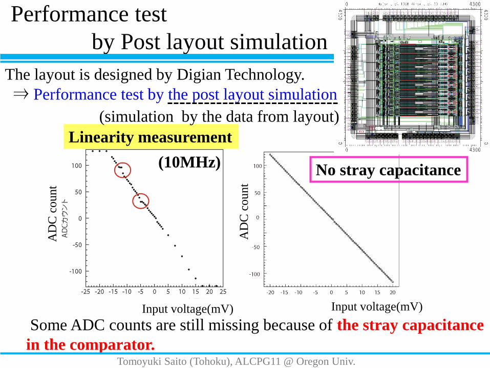
The layout is designed by Digian Technology.
⇒ Performance test by the post layout simulation
Input voltage(mV)
AD
Cco
un
t
Linearity measurement
(10MHz)
(simulation by the data from layout)
Tomoyuki Saito (Tohoku), ALCPG11 @ Oregon Univ.
Performance test
by Post layout simulation
30
The layout is designed by Digian Technology.
⇒ Performance test by the post layout simulation
Input voltage(mV) Input voltage(mV)
AD
Cco
un
t
AD
Cco
unt
Some ADC counts are still missing because of the stray capacitance
in the comparator.
Linearity measurement
No stray capacitance(10MHz)
Tomoyuki Saito (Tohoku), ALCPG11 @ Oregon Univ.
(simulation by the data from layout)
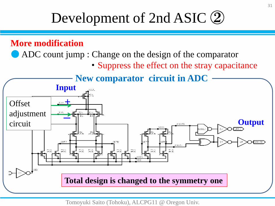
Development of 2nd ASIC ②
Input
Output
Total design is changed to the symmetry one
31
More modification
● ADC count jump : Change on the design of the comparator
・Suppress the effect on the stray capacitance
+
-
Offset
adjustment
circuit
New comparator circuit in ADC
Tomoyuki Saito (Tohoku), ALCPG11 @ Oregon Univ.
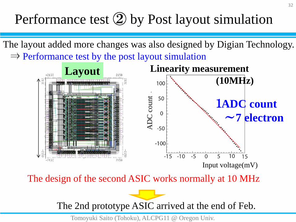
Performance test ② by Post layout simulation
Layout Linearity measurement
(10MHz)
The 2nd prototype ASIC arrived at the end of Feb.
1ADC count
~7 electron
32
The layout added more changes was also designed by Digian Technology.
⇒ Performance test by the post layout simulation
Input voltage(mV)
AD
Cco
un
t
The design of the second ASIC works normally at 10 MHz
Tomoyuki Saito (Tohoku), ALCPG11 @ Oregon Univ.
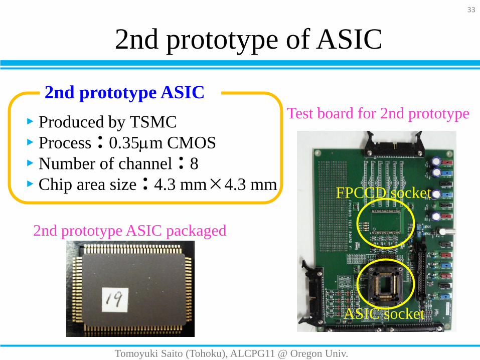
2nd prototype ASIC packaged
Test board for 2nd prototype
33
2nd prototype of ASIC
ASIC socket
FPCCD socket
▸ Produced by TSMC
▸ Process:0.35mm CMOS
▸ Number of channel:8
▸ Chip area size:4.3 mm×4.3 mm
2nd prototype ASIC
Tomoyuki Saito (Tohoku), ALCPG11 @ Oregon Univ.
34
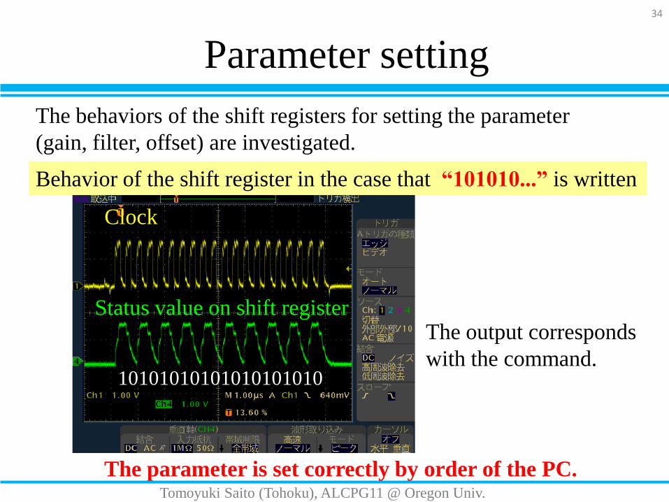
Parameter setting
Clock
Status value on shift register
The behaviors of the shift registers for setting the parameter
(gain, filter, offset) are investigated.
Behavior of the shift register in the case that “101010...” is written
The parameter is set correctly by order of the PC.
10101010101010101010
The output corresponds
with the command.
Tomoyuki Saito (Tohoku), ALCPG11 @ Oregon Univ.
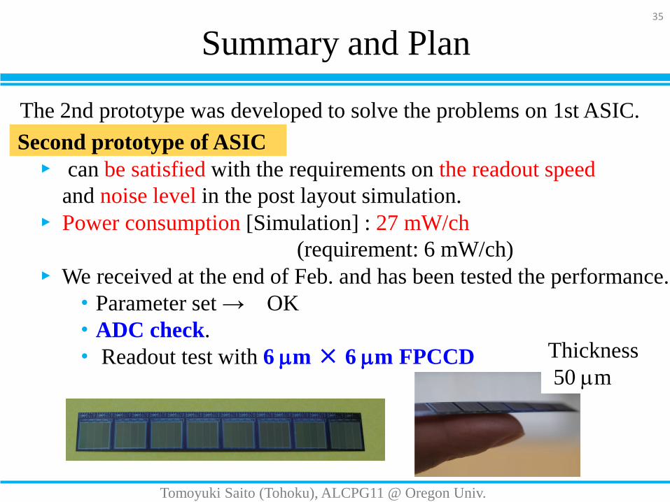
Summary and Plan35
Second prototype of ASIC
► can be satisfied with the requirements on the readout speed
and noise level in the post layout simulation.
► Power consumption [Simulation] : 27 mW/ch
(requirement: 6 mW/ch)
► We received at the end of Feb. and has been tested the performance.
・Parameter set → OK
・ADC check.
・ Readout test with 6 mm × 6 mm FPCCD
The 2nd prototype was developed to solve the problems on 1st ASIC.
Tomoyuki Saito (Tohoku), ALCPG11 @ Oregon Univ.
Thickness
50 mm

Back up
37
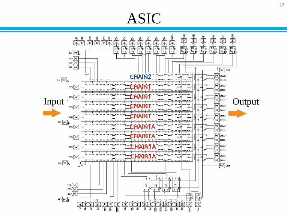
ASIC
OutputInput
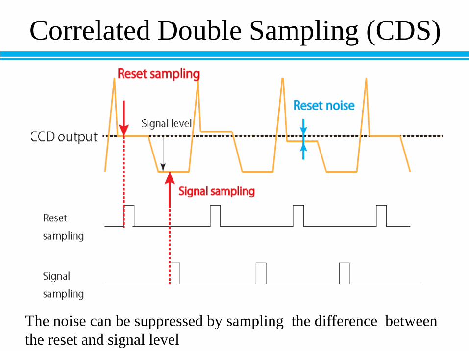
Correlated Double Sampling (CDS)
The noise can be suppressed by sampling the difference between
the reset and signal level
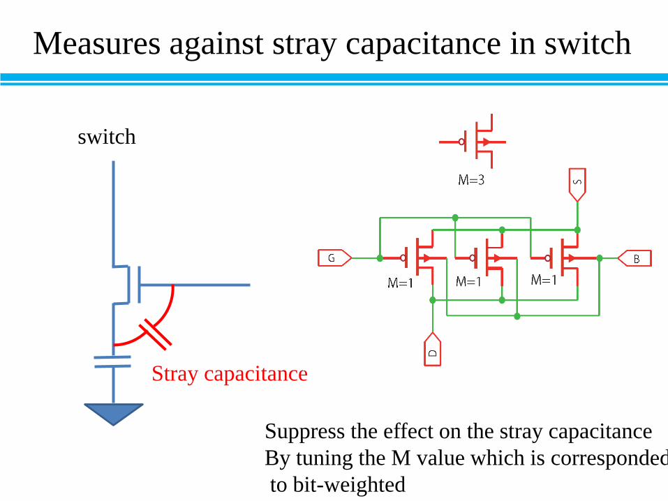
Measures against stray capacitance in switch
Stray capacitance
Suppress the effect on the stray capacitance
By tuning the M value which is corresponded
to bit-weighted
switch
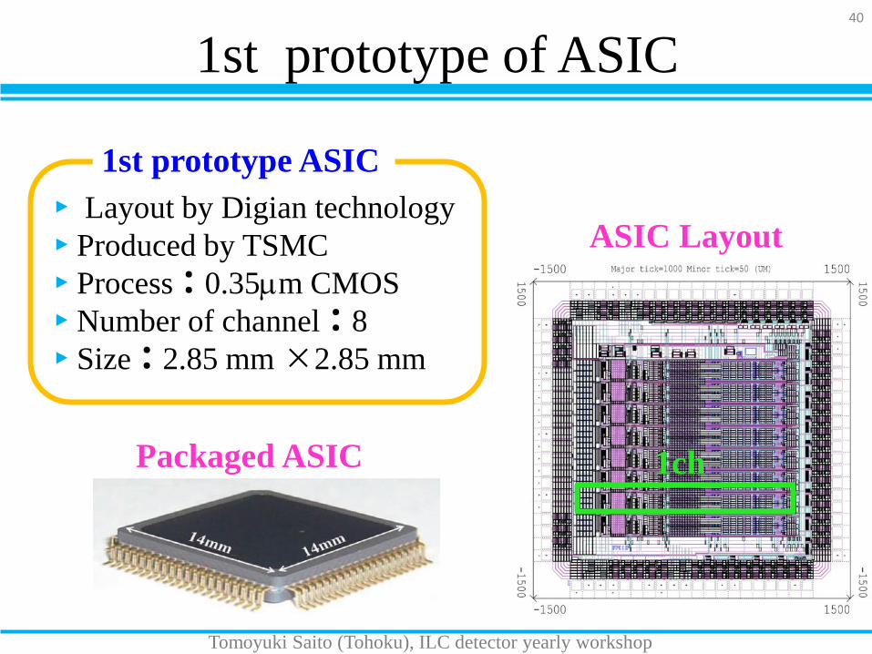
1st prototype of ASIC
ASIC Layout
40
▸ Layout by Digian technology
▸ Produced by TSMC
▸ Process:0.35mm CMOS
▸ Number of channel:8
▸ Size:2.85 mm ×2.85 mm
1chPackaged ASIC
1st prototype ASIC
Tomoyuki Saito (Tohoku), ILC detector yearly workshop
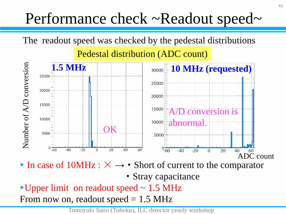
Performance check ~Readout speed~
The readout speed was checked by the pedestal distributions
ADC count
Nu
mb
er o
f A
/D c
on
ver
sion
OK
A/D conversion is
abnormal.
Pedestal distribution (ADC count)
► In case of 10MHz : × → ・ Short of current to the comparator
・ Stray capacitance
►Upper limit on readout speed ~ 1.5 MHz
From now on, readout speed = 1.5 MHz
41
Tomoyuki Saito (Tohoku), ILC detector yearly workshop
1.5 MHz 10 MHz (requested)
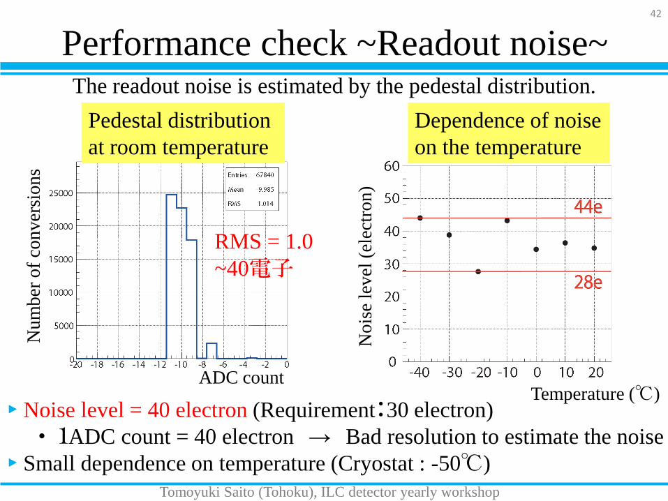
Performance check ~Readout noise~
Pedestal distribution
at room temperature
ADC count
Nu
mber
of
con
ver
sio
ns
RMS = 1.0
~40電子
The readout noise is estimated by the pedestal distribution.
Dependence of noise
on the temperature
► Noise level = 40 electron (Requirement:30 electron)
・ 1ADC count = 40 electron → Bad resolution to estimate the noise
► Small dependence on temperature (Cryostat : -50℃)
42
No
ise
lev
el (
elec
tro
n)
Temperature (℃)
Tomoyuki Saito (Tohoku), ILC detector yearly workshop
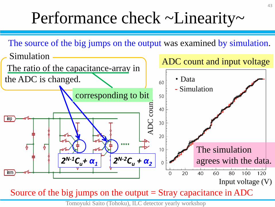
Performance check ~Linearity~
・ Data
- Simulation
The simulation
agrees with the data.
Source of the big jumps on the output = Stray capacitance in ADC
2N-1Cu+ α1 2N-2Cu + α2
43
The source of the big jumps on the output was examined by simulation.
ADC count and input voltage
Input voltage (V)
AD
C c
ou
nt
The ratio of the capacitance-array in
the ADC is changed.
Simulation
corresponding to bit
Tomoyuki Saito (Tohoku), ILC detector yearly workshop