Embed Size (px)
Citation preview
Comput. & Elect. Engng, Vol. 3, pp. 35-51. Pergamon Press, 1976. Printed in Great Britain
D I G I T A L A N A L Y S I S O F O P T I C A L T R A N S F O R M S
A N D C O R R E L A T I O N S
DAVID CASASENT a n d WARREN STERLING'~
Department of Electrical Engineering, Carnegie-Mellon University, Pittsburgh, PA 15213, U.S.A.
(Received 28 April 1975)
Abstract--Hardware, applications and experimental results for an interface from an optical processor to a digital computer are described. The interface analyzes the contents of the Fourier transform and correlation planes of an optical processor displays and stores various representations of the data in these planes, controls the format and contents of the input and matched spatial filter planes of the optical processor, and by digital feedback controls the throughput and operation of the optical processor. A hybrid optical/digital processor and a programmable optical processor result. Much of the interface is constructed from existing computer modules.
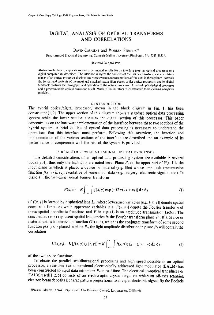
1. INTRODUCTION The hybrid optical/digital processor, shown in the block diagram in Fig. 1, has been constructed/l, 2]. The upper section of this diagram shows a standard optical data processing system while the lower section contains the digital section of this processor. This paper concentrates on the hardware implementation of the interface between these two sections of the hybrid system. A brief outline of optical data processing is necessary to understand the operations that this interface must perform. Following this overview, the function and implementation of the various sections of the interface are described and an example of its performance in conjunction with the rest of the system is provided.
2. REAL-TIME TWO-DIMENSIONAL OPTICAL PROCESSOR
The detailed considerations of an optical data processing system are available in several books[3, 4], thus only the highlights are noted here. Plane Po in the upper part of Fig. 1 is the input plane in which is placed a device or material (e.g. film) whose amplitude transmission function f(x, y) is representative of some input data (e.g. imagery, electronic signals, etc.). In plane P~, the two-dimensional Fourier transform
F(u,v)= E f ~ f f(x,y)exp[-j2"n'(ux + vy)]dx dy (1)
of f(x, y) is formed by a spherical lens L~, where lowercase variables [e.g. f(x, y)] denote spatial coordinate functions while uppercase variables [e.g. F(u, v)] denote the Fourier transform of these spatial coordinate functions and E in eqn (1) is an amplitude transmission factor. The coordinates (u, v) represent spatial frequencies in the Fourier transform plane PI. If a device or material with a transmission function G*(u, v), which is the conjugate transform of some second function g(x, y), is placed in plane P~, the light amplitude distribution in plane P2 will contain the correlation
U(x2y2) = K[f(x, y)*g(x, y ) ] = K f r(x, y)g(x - /~, y -'o) dx dy (2)
of the two space functions.
To obtain the parallel two-dimensional processing and high speed possible in an optical processor, a real-time two-dimensional electronically addressed light modulator (EALM) has been constructed to input data into plane Po in real-time. The electrical-to-optical t ransducer or EALM used / l , 2,5] consists of an electro-optic crystal target on which an off-axis scanning electron beam deposits a charge pattern proportional to an input electronic signal. By the Pockeis
tPresent address: Xerox Corp., (PaiD Alto Research Center), Los Angeles, California.
35
36 I) ( \5~SINI ;lllt] W, N~IRiI',{,
loser beam l _ _ . ~ -_ :: : _ . - v idicon
o n l i l e LI I ] i L2 * video input
. . . . o p t i c a l / d i g i t a l I V i
. o r , . . . . . . , . t , . , c . . . i t o q
,,, , , , , , - F _ . p a ; ; ; ]
Fig. I. Block diagram of the hybrid optical/digilal procc-,,,or. ( ontrul paths ate q~o,~ t+ and Iclclcncc beam i~ omined for simplicity. Code: EAIM. eledronically -addressed light modul'alor: ()+~,1 M. npti,:0!y-addre~,ed
lighl modulalor; 4/D, analog-lo-dililal converte~: D/4, digilal-to-;tnal.g converter
effect[6], this charge pattern produces a spatial modulation of the amplitude or phase of a collimated laser beam that passes through the target crystal. The input pattern is written or scanned at television frame rates (for convenience onlyl at 3{) frames/see in a 2:1 interlaced format. Various potential real-time optically addressed light modulators (()AI+Ms) for use in recording the required matched spatial filter G*(u, v) for plane P, arc in various stages of development. During the vertical retrace time of a standard television frame, the input data f (x,y) on the EALM is read and processed (i.e. the laser beam is pulsed on}, The Fourier transform F(u, t:) appears in plane P, and the correlation of fix, y) and V(x, y ) appears in plane Pc. Vidicons, synchronized with the scan rate of input transducer, arc focused on planes P, and P> During the last half of vertical blanking time, the charge pattern on the crystal is erased by secondary emission using st second flood electron gun.
~. O P T I ( g l / D I ( I I I A I I N I E R F M I I
The optical system description in Section 2 was necessary to place the various operations and functions that the optical/digital interface must perform in perspective File iighl distribution in the Fourier transform plane consists of a series of peaks of light. Their locations in plane P, correspond to various spatial frequent,, components in tile input, while the amplitude of the light at a point in plane P, is a measure of the amount of thal particular frequent} component that is present in the input (i.e. the magnitude of the corresponding Fourier coefficient in the Fourier series expansion of the input function). The presence and amount of various spatial frequency components and bands of spatial frequencies has been shown to be important in various image, information, and signal processing problemsl71.
The light distribution in the correlation plane P~ also consists of peaks of light. In this case, each point in plane P~ corresponds to a particular location in the input image in plane P,>. A peak of light in plane P~ indicates that the function ,.,,Ix. y! [whose conjugalc t~',m.,form G*{u, v l was placed in plane P,] exists in the input function ./(x, y)al a l o c a t i o n determined t~v the coordinate,,, of the peak in the correlation plane. The amplitude of this correlati,m peak > ~t measure of the degree of similarity or correlation between ,e(-~, v land thc :cotton of (( v. v! under consideration.
One obvious function of the optical/digital interface is the extraction of the amplitude and location of the "importanf" peaks of light in planes I', at~d P,. Which peaks are "important" depends greatly on the system's specific application. The purpose of this paper is to report on the hardware and design of the interface, rather than the systenfs applications. Nonetheless, system applications cannot go unmentioned. Those applications that ha~e been and are being investigated include: area correlation [81, missile guidance [51, reconnaisance, text correlation[9], photogrammetry, contour plotting, pmallax exm~ction1101, linear and planar phased array data processing[l I} and pulsed Doppler and FM step radm signal processmg1121, among others.
In the initial stage of radar processing, the coordinates of the firsl-order fringe term in the
Digital analysis of optical transforms and correlations 37
transform of properly formated radar data yields information on the azimuth, elevation, velocity or range of the target [11, 12]. In this case the section of the transform plane that must be scanned to locate the spot corresponding to the target in question is determined by the specifications of the radar system. This application will serve to demonstrate several other functions of the interface. Since a d.c. term will be present in the transform plane, the interface should have the ability to subtract two frames to remove this d.c. term and enhance target detection. In addition, it is intended that one processor (optical) under control of a digital computer be used to process returns from both primary and secondary radars. The scan format is different for each radar system and this must be controlled by the digital section of the hybrid processor. Furthermore, the data from one radar should be used to aid secondary radars; in this mode, the digital feedback (shown in Fig. 1) from the transform plane through the digital section of the processor and back to the input modulator or to the radar itself is utilized. Radar also serves as an example of several displays that are of use. If the digital section of the system can store the location of the target (the location of the first-order fringe term), the target's time history in azimuth, range, etc. can easily be displayed.
The final version of this optical processor for radar data would use the powerful holographic correlation property of an optical system. In various versions of this scheme, spatial filters would be used to enhance signal-to-noise ratio and to increase the system's computing power by providing both range and azimuth data from one system. In these cases, the correlation plane (P2 in Fig. 1) is analyzed by the interface and the contents of the spatial filter plane altered under computer control using the results present in the correlation plane. Similar schemes are of use in all image correlation applications when the size and orientation of the target cause degradations in the signal-to-noise ratio of the correlation peak. To be compatible with the throughput of the input EALM, the interface must perform these operations in 33.3 msec (one television frame time). The resolution, threshold levels, and all control functions of the interface must be under program control from a supporting minicomputer as well as under operator control.
These necessary operations and functions of the interface (and digital section) are summarized below.
(1) Extract the coordinates and amplitude of the "important" points in the transform and correlation plane.
(2) Extract the coordinates of all points of high light intensity in the transform and correlation planes while rejecting points of lower intensity.
(3) Subtract, add and store frames of imagery. (4) Display binary-digitized versions of transform and correlation plane light amplitude
distributions as well as other versions and combinations of these binary digitized images. (5) Control scan rates and format of input EALM and content and format of the spatial filter
plane.
Design philosophy The block diagram of the optical/digital interface is shown in Fig. 2. The remainder of the
digital section of the hybrid processor consists of:
(1) A PDP-ll/15 minicomputer with 12K of core. (2) A high-speed DRll-B interface that provides direct memory access to the PDP-I1/15. (3) An X - Y CRT display. (4) A teletype and paper tape rader.
Figure 3 is a photograph of the digital section of the processor. The remainder of this paper concentrates on the elements of the optical digital interface itself and how it communicates with the other devices in the system.
The interface (Fig. 2) consists of three sections:
(1) Vidicon interface (2) Video processor (3) Digital interface and control.
Although this interface is presently dedicated to use with our optical processor and

38 D. (',~SASFNr and W. S'IfRI J N ( ;
master svnc~] generator . . . . . . . . . j
r ~ . . . . . . . . . . . . . . . . . . . . . . . . . . . .
I ' I / d " " to '~ o p t i c a Jgltal interface t
.den I / [ . . . . 7 I - - , " i n ] - - ~ I n CO .o . ,e , f l d,,,,a, I I d e v i c e I / interface I I v i d e o I • . . J
to i I co"trot I I I I svnc L . ] cnT - - - , - : -1 I [ 1 I . .ara,nr t -
display L - - - - - ' = . . . . . . . . - J
. . . . t . . . . . . . . . . t . . . . . . . . . . . . . from PDP-II to POP II
Fig. 2. Block diagram of the optical-digital interface
Fig. 3. Photograph of the digital section of the hybrid processor. From left to right: monitor, .\- "~ CRI'. optical/digital interface, teletype, PDP-11/15 minicomputer
PDP-I 1/15 support computer, the device is quite general and can be used anytime optical data must be digitally analyzed or displayed. As indicated in Fig. 1, vidicons :ire the connecting link between the optical and digital sections of the processor. These can be replaced by higher resolution units, units with extended dynamic range, or charge coupled device arrays, etc. as the application warrants. In its present version, these vidicons continuously scan the contents of planes P~ and P2 (Fig. 1) in a 525 line. raster scan, 2 : 1 interlaced mode at a rate of 30 frame/see. The AGC on these units has been disabled to allow them to record true incident light levels. To enable these vidicons to remain in phase with the scan of the input EAIM, their sync signals are derived from a master system sync generator.
The vidicon interface section (Fig. 2) transforms the output video signal from the vidicon into a bit pattern. The final binary-digitized image is formed in the video processor section from where it is transferred to the PDP-II/15 for storage or display or for analysis and use in controlling the optical processor. The digital interface and control section accepts commands from the PDP-I 1/15 and controls all parts of the system (vidicon interface, video processor, CRT display, video storage, EAI,M, OAIM, etc.).
The timing for the vidicon interface and video processor sections is derived from the horizontal and vertical sync and blanking signals. These signals can be provided by the master sync generator (see Fig. 2), however for generality a sync separator (see Fig. 2) is available to produce these timing pulses from the composite video output of the vidicon.
To obtain the desired results, the following binary-digitization process is performed on each frame.
Digital analysis of optical transforms and correlations 39
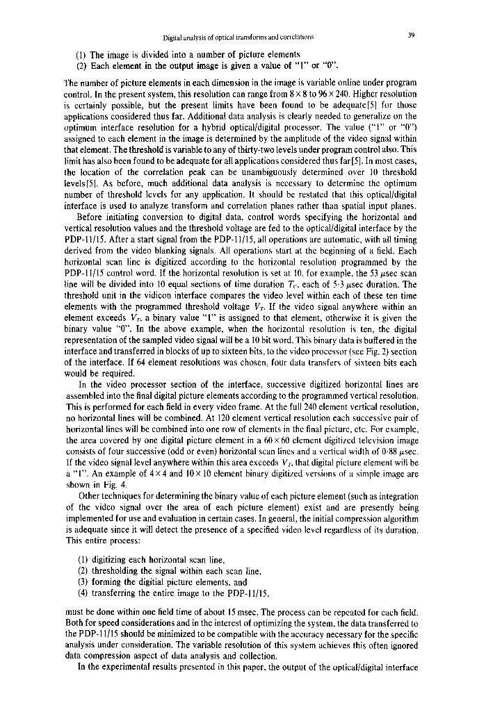
(1) The image is divided into a number of picture elements (2) Each element in the output image is given a value of "1" or "0".
The number of picture elements in each dimension in the image is variable online under program control. In the present system, this resolution can range from 8 × 8 to 96 x 240. Higher resolution is certainly possible, but the present limits have been found to be adequate[5] for those applications considered thus far. Additional data analysis is clearly needed to generalize on the optimum interface resolution for a hybrid optical/digital processor. The value ("1" or "0") assigned to each element in the image is determined by the amplitude of the video signal within that element. The threshold is variable to any of thirty-two levels under program control also. This limit has also been found to be adequate for all applications considered thus far[5]. In most cases, the location of the correlation peak can be unambiguously determined over 10 threshold levels[5]. As before, much additional data analysis is necessary to determine the optimum number of threshold levels for any application. It should be restated that this optical/digital interface is used to analyze transform and correlation planes rather than spatial input planes.
Before initiating conversion to digital data, control words specifying the horizontal and vertical resolution values and the threshold voltage are fed to the optical/digital interface by the PDP-11/15. After a start signal from the PDP-11/15, all operations are automatic, with all timing derived from the video blanking signals. All operations start at the beginning of a field. Each horizontal scan line is digitized according to the horizontal resolution programmed by the PDP-11/15 control word. If the horizontal resolution is set at 10, for example, the 53/zsec scan line will be divided into 10 equal sections of time duration Tc,, each of 5.3/~sec duration. The threshold unit in the vidicon interface compares the video level within each of these ten time elements with the programmed threshold voltage VT. If the video signal anywhere within an element exceeds VT, a binary value "1" is assigned to that element, otherwise it is given the binary value "0". In the above example, when the horizontal resolution is ten, the digital representation of the sampled video signal will be a 10 bit word. This binary data is buffered in the interface and transferred in blocks of up to sixteen bits, to the video processor (see Fig. 2) section of the interface. If 64 element resolutions was chosen, four data transfers of sixteen bits each would be required.
In the video processor section of the interface, successive digitized horizontal lines are assembled into the final digital picture elements according to the programmed vertical resolution. This is performed for each field in every video frame. At the full 240 element vertical resolution, no horizontal lines will be combined. At 120 element vertical resolution each successive pair of horizontal lines will be combined into one row of elements in the final picture, etc. For example, the area covered by one digital picture element in a 60 × 60 element digitized television image consists of four successive (odd or even) horizontal scan lines and a vertical width of 0.88/zsec. If the video signal level anywhere within this area exceeds VT, that digital picture element will be a "1". An example of 4 × 4 and 10 x 10 element binary digitized versions of a simple image are shown in Fig. 4.
Other techniques for determining the binary value of each picture element (such as integration of the video signal over the area of each picture element) exist and are presently being implemented for use and evaluation in certain cases. In general, the initial compression algorithm is adequate since it will detect the presence of a specified video level regardless of its duration. This entire process:
(1) digitizing each horizontal scan line, (2) thresholding the signal within each scan line, (3) forming the digitial picture elements, and (4) transferring the entire image to the PDP-11/15,
must be done within one field time of about 15 msec. The process can be repeated for each field. Both for speed considerations and in the interest of optimizing the system, the data transferred to the PDP-11/15 should be minimized to be compatible with the accuracy necessary for the specific analysis under consideration. The variable resolution of this system achieves this often ignored data compression aspect of data analysis and collection.
In the experimental results presented in this paper, the output of the optical/digital interface
40 1). ('ASASENI and W. S'[ERIIN(;
0
o ooo~o0 iooooo i o 0 o o 6
~ i ! I i i o 0 o o 0 oo~0oo ooooo~ oo ~o~ o 0oo
Image 4 1 4 10 z 10
Fig. 4. Example to demonstrate the concept of a binary-digitized image. (at input, (hi binar},-digitized image of (a) with 4 × 4 resolution. (c) binary-digitized image of (a) with 10 ~ 10 restflution.
will be displayed on a CRT. The display can be on line, displaying each digital image as it is generated, or off line, displaying an image other than the one just generated. The only limitation imposed on the number of images stored and displayed is the memory capacity of the PDP-11/15.
These descriptions of each of the sections of the optical digital interface were purposely brief to provide a general idea of the operations each section must perform and the required interaction between all sections. The detailed design of each of these sections will now be considered.
4 ~ I D I ( ' O N I N T E R F A ( ' E
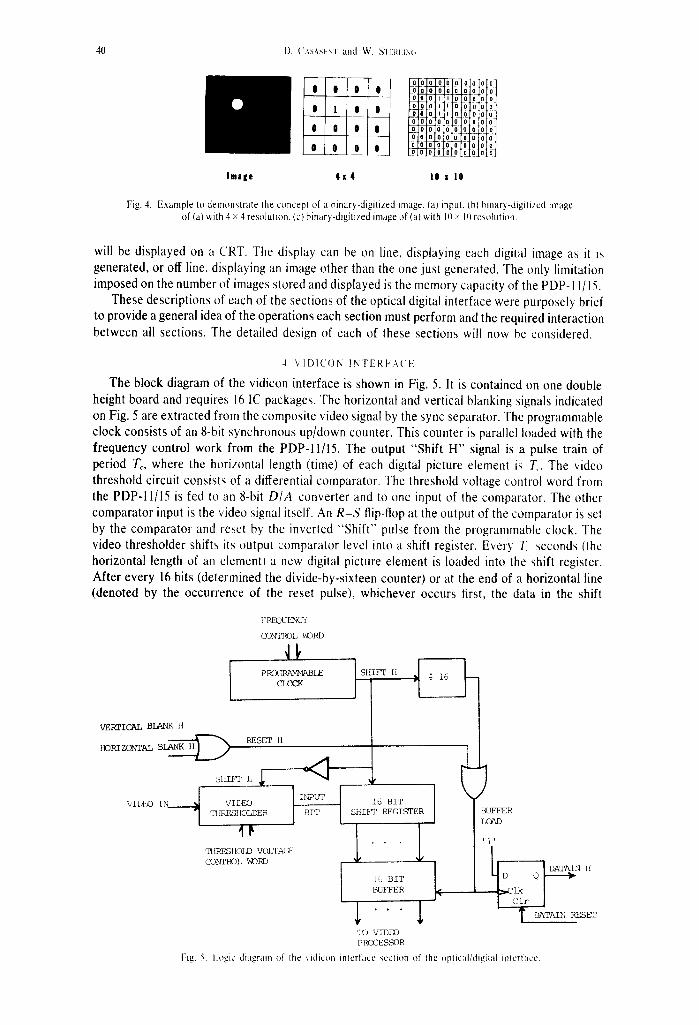
The block diagram of the vidicon interface is shown in Fig. 5;. It is contained on one double height board and requires 16 IC packages. The horizontal and vertical blanking signals indicated on Fig. 5 are extracted from the composite video signal by the sync separator. The programmable clock consists of an g-bit synchronous up/down counter. This counter is parallel loaded with the frequency control work from the PDP-II/15. The output "Shift H" signal is a pulse train of period To, where the horizontal length (time) of each digital picture element is T,. The video threshold circuit consists of a differential comparator. The threshold voltage control word from the PDP-11/15 is fed to an 8-bit D/A converter and to one input of the comparator. The other comparator input is the video signal itself. An R-S flip-flop at the output of the comparator is set by the comparator and reset by the inverted "Shift" pulse from the programmable clock. The video thresholder shifts its output comparator level into a shift register. Every T, seconds (the horizontal length of an element) a new digital picture element is loaded into the shift register. After every 16 bits (determined the divide-by-sixteen counter) or at the end of a horizontal line (denoted by the occurrence of the reset pulse), whichever occurs first, the data in the shift
~ L ~DRD
VE~ICAL BIANK H
HORIZONTAL
Sliff~f L {
~IDEO I ~ VIDEO TI ffIESHOLDER
THRt~ HOL£) VC)LTA( ~2 GO~'Tf I~O L WORD
L6 BIT SHIEr REGISTER
I l I LG BIT
BUFFER
'~.) VIDEO PRCCESSOR
I
~ R
~ - - ~ DATAIN H
I DATAIN RESET
Fig. 5. lx~gic diagraln of the ,,idicon interface ,,ection of the optical/digital interlace.

Digital analysis of optical transforms and correlations 41
register is transferrred to the 16-bit buffer. The "Datain" flag is then set, signaling the video processor that a data word is available.
5. REGISTER TRANSFER MODULES (RTM's)
As previously noted, the video processor and digital interface sections of the optical/digital interface are constructed from existing modular computer elements, referred to as RTM's (Register Transfer Modules). Before detailing the remainder of the interface design, a brief explanation of RTM's is necessary. A more extensive description of these modules and their use is available in the literature[13, 14].
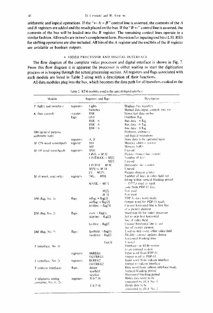
An RTM system consists of data and control modules connected to a common 21 line data bus. Sixteen of these lines are data lines while the remaining 5 provide synchronization signals, power clear, and an overflow bit. Each module can store and/or operate on one or more words (16 bits) or bytes (8 bits) of data. Data words are transferred between these modules by the data bus. The five main types of RTM's are listed in Table 1 using the PMS notation[15]. The module examples referred to in this table are explained more fully in subsequent sections. Most modules have control inputs which are used to evoke the various logical operations of data transfers. Only one module DM (General Purpose Arithmetic Unit), generally denoted by DM (gpa), is discussed in detail here as an example. All modules except the T (Vidicon Interface), T (sync separator), and T (D/A converter) are explained fully in Ref. [13]. The T (Vidicon Interface) and T (syn separator) were discussed in Sections 4 and 3 respectively. The T (D/A convertor) is a dual 10 V output D/A converter with special bus interfacing added. Various control modules (Ke, Kb, etc.) will be explained after the RTM hardware design is presented. This will allow the use of examples directly from the interface hardware.
The DM (General Purpose Arithmetic Unit) is shown in Fig. 6. This is the major module of any RTM system. It can store two words of data in registers A and B, and perform 11 different
~ A ~ B
~ - ' ~ B ~ A + I ~ A - 1 ~ A x 2 ~A ^B --A vB ~ A ® B - -A+B ~A - B
A-- B ~
R E S U L T / 2 LS'I" b RS'I" b
bus
H DM (general purpose
ari thmetic unit)
A < 1 5 : 0 >
B < ' f S : 0 >
b A<15 :O> ID
b B<15> ; B<O>
Fig. 6. The DM (general purpose arithmetic unit) RTM module. Control inputs, registers, and Boolean outputs are shown.
Table I. Types of RTM modules
Type Description Example
M (memory) stores data M (array: 256w) D (data) performs data operations D (NAND)
(arithmetic, logical, decoding, etc.) DM (data-memory) stores data and performs DM (general purpose
operations arithmetic unit) T (transducer) changes data to encode a 7" (vidicon interface)
given meaning in some new T (D/A converter) form (voltage to bit pattern, etc.)
K (control) evokes operations of other K (bus) components in the system Ke, Kb, Ksub
42 D. ('ASASENT and W. SrF:RLIm;
arithmetic and logical operations. If the %-A + B" control line is asserted, the contents of the A and B registers are added and the result placed on the bus. If the "B ~ " control line is asserted, the contents of the bus will be loaded into the B register. The remaining control lines operate in a similar fashion. All results are in two's complement form. Provision for inputing end bits (LSI, RSI) for shifting operations are also included. All bits of the A register and the end bits of the B register are available as boolean outputs.
6. V I D E O P R O C E S S O R A N D D I G I T A l . I N T E R F A C E
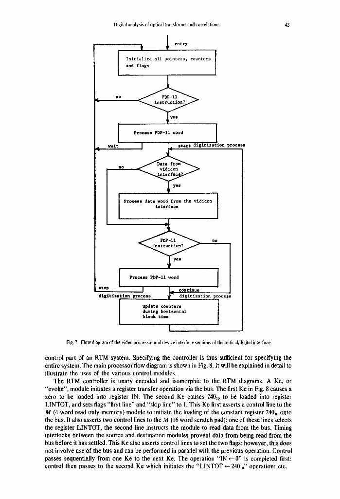
The flow diagram of the complete video processor and digital interface is shown in Fig. 7. From this flow diagram it is apparent the processor is either waiting to start the digitization process or is looping through the actual processing section. All registers and flags associated with each module are listed in Table 2 along with a description of their functions.
All data modules plug into the bus, which becomes the data path for all transfers evoked in the
Table 2. RTM modules used in the optical/digital interface
Module Registers and flags Description
T (lights and switches) registers:
K Ibus control) register: flags:
DM (general purpose arithmetic unit)
registers: M (256 word scratchpad) register:
M (16 word scratchpadl registers:
M (4 word; read only) registers
DM (flag, No. I/ flags:
DM (flag, No. 2) flags:
DM (flag. No. 3i flags:
T (interface, No. I)
T (interface. No. 2)
T (vidicon interface)
T (digital-to analog converter, No. I.. 2)
registers:
registers:
flags:
registers:
l,ights Displays bus Iransfers Switches Manual data input, controls bus use BSR Stores lasl dam on bus OVF Overflow flag B S R - 0 Bus data = 0 flag BSR >0 Bus data 0 flag BSR 11 Flus data. 0 flag
Performs arithmetic and logical operations
A. B Store data to be operated upon MA Memory address pointer MB Memor5 buffer M]O] Unused I,INE: Mil l Picture ele]uctll hne cuuntet I I N E M A X : - M[21 Number of line,
M[3] Llnused I,INTOT: : M[4I Horizontal line cmmtct .'~1151 to M[141 Unused IN: - M[15] Picture element puintel 24(!,,,: M[0] Number of lines in video field not
falling within vertical hhmking period MASK: M{I] { :17777,,1used to mask
co, de from PDP-II data M [21 Not used M[3I Not used
inflag: flagll I PI)P-I l data word read} outflag: flag[2] Output word for PDP-II ready firstl ine:- flag[3] ( 'urrent horizontal line is first line
of a picture element s l a r h - flag[ll Start/slOp bil for video processor skipline: f lag[2l Set to skip first horizontal
line of video field k~stline:- flag[3] Current hori/ontal line is last
line of picture dement lirstfield: : flag[ll [ised to skip every other video field linedone: - flag[2] Disables counter updates during
horizontal blanking time flag[3] I nused
Interfaces an RTM system to a n exlerna] s~stem
INREGI Input v, ord from PDP-II OUTREGI Output word to PDP-II INREG2 Input word f rom xidicon interface OUTREG2 Outpu! Io vidicon interface datain l)ata word from vidicon interface read}, newfield Vertical blanking period newline Huriz,.',ntal bkmking period XA(7:0) Holds data word to be
converted by I l i a No. t YA(7:0) Holds data to be
converted by D/A No. 2
Digital analysis of optical transforms and correlations 43
A watt
~ entry
Inltlalize all pointers, counters
and f l a g s
Q o
n o
i
Process PDP-11 word [
J 1~ start digittza~ion
@ Process data word from the v l d l c o n
i n t e r f a c e
p r o c e s s
n o
i Process PDP-11 word
s top ~ [_ continue dtstttzet~on process ~" digitization process
update counters [ during horlzoncal blank tlme
[
Fig. 7. Flow diagram of the video processor and device interface sections of the optical/digital interface.
control part of an RTM system. Specifying the controller is thus sufficient for specifying the entire system. The main processor flow diagram is shown in Fig. 8. It will be explained in detail to illustrate the uses of the various control modules.
The RTM controller is unary encoded and isomorphic to the RTM diagrams. A Ke, or "evoke", module initiates a register transfer operation via the bus. The first Ke in Fig. 8 causes a zero to be loaded into register IN. The second Ke causes 240,0 to be loaded into register LINTOT, and sets flags "first line" and "skip line" to 1. This Ke first asserts a control line to the M (4 word read only memory) module to initiate the loading of the constant register 240,0 onto the bus. It also asserts two control lines to the M (16 word scratch pad): one of these lines selects the register LINTOT, the second line instructs the module to read data from the bus. Timing interlocks between the source and destination modules provent data from being read from the bus before it has settled. This Ke also asserts control lines to set the two flags: however, this does not involve use of the bus and can be performed in parallel with the previous operation. Control passes sequentially from one Ke to the next Ke. The operation "IN ~ 0" is completed first: control then passes to the second Ke which initiates the "LINTOT ~ 240,o" operation: etc.
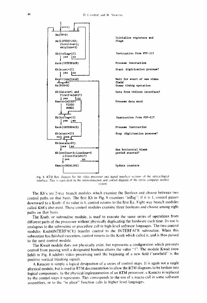
44 1). ('ASASEN'I and W, SF~:Rz i~(;
-7 Ke(IN*-0)
Ke(LINTOT÷240; f i r s t l i n e * l ; skipline~l)
Kb(inflag~l?) ] Yes In°
Ksub(INTERFACE)
KS(start-l?) I yes [no
K~fleld)
Ke(BSR÷B)
Kb(dataln-I and firstfield-l?)
yes [no Kmacro(ACCEPT '
I VIDEO WORD)
I_ I
Kb(inflag-l?) J yes [no
Ksub(INTERYACE)
Kb(start-l?)
yea [no
Kb(newl ine- la l inedone-1 A f i r s t f t e l d - l ? ) l yes no
Kmacro(NEWLINE)
I
I n i t i a l i z e r e g i s t e r s and f l a g s
Inetruction from Ir~P-117
Process i n s t r u c t i o n
Start digitization process?
Wait for s tar t of new video field Dummy timing operation
Data from vidicon i n t e r f a c e ?
Process data word
Instruction from PDP-II?
Process instruction
Stop digitization process?
Has h o r i z o n t a l blank period started?
Update counters
Fig. 8. RTM flow diagram for the video processor and digital interface sections of the optical/digital inlerface. This is equivalent to the interconnection and control diagram of the entire computer modnle
system
The Kb's are 2-way branch modules which examine the Boolean and choose between two control paths on that basis. The first Kb in Fig. 8 examines "inflag": if it is I, control passes downward to a Ksub: if its value is 0, control returns to the first Ke. Eight-way branch modules called Kb8's also exist. These control modules examine three booleans and choose among eight paths on that basis.
The Ksub, or subroutine module, is used to execute the same series of operations from different parts of the processor without physically duplicating the hardware each time. Its use is analagous to the subroutine or procedure call in high-level software languages. The two control modules Ksub(1NTERFACE) transfer control to the INTERFACE subroutine. When this subroutine has finished execution, control returns to the Ksub which called it, and is then passed to the next control module.
The Kwait module does not physically exist, but represents a configuration which prevents control from passing until a designated boolean attains the value "1". The module Kwait (new field) in Fig. 8 inhibits video processing until the beginning of a new field ("newfield" is the
positive vertical blanking signal). A Kmacro is simply a logical designation of a series of control steps. It is again not a single
physical module, but is used in RTM documentation to allow the RTM diagrams to be broken into logical components. In the physical implementation of an RTM processor, a Kmacro is replaced by the control steps it represents. This corresponds to the use of a macro call in some software assemblers, or to the "'in place" function calls in higher level languages.
Digital analysis of optical transforms and correlations 45
When first started, the processor in Fig. 8 enters an initialization and wait state. Control data from the PDP-I 1/15 can be processed by Ksub(INTERFACE) during this state. When a start signal is received, the prcessor begins building the binary digitized image as soon as a new video field starts. Control words from the PDP-11/15 can be accepted during the digitization process. If a stop signal is received, control returns to the initialization state. The hardware subroutine Ksub(INTERFACE) comprises the digital interface and control section of the block diagram in Fig. 2. It decodes instructions from the PDP-II/15 and loads the appropriate registers. Instructions from the PDP-11/15 consist of 16 bits, a three-bit code and 13 bits of data. Only four of the possible seven codes are currently used. The four data types are:
1. Vidicon Interface Control Word 2. Lines per Picture Element 3. Start/Stop Code 4. CRT Display Data
The macro Kmacro (DISPLAY) drives the CRT display. When the code for "CRT Display Data" is decoded, this macro is used. The contents of bit 12 denote whether the data is loaded into the X or Y deflection registers. The amount of deflection is determined by the lower order bits of the control word. The low order bytes are loaded into the X or Y deflection D/A.
The macro, Kmacro (ACCEPT VIDEO WORD), accepts data from the vidicon interface and forms the final binary picture elements. A partially completed row of picture elements is stored in memory. When data from the next horizontal scan line is available, each bit is OR'ed with its corresponding partially completed picture element. When the row of picture elements is complete (the last horizontal scan line comprising that row of elements has been digitized), the picture elements are transferred to the PDP-I1/15.
The macro, Kmacro(NEWLINE), is executed only during the horizontal blanking period and performs the following functions:
(1) Flags the first and last horizontal scan lines of the picture element. The flags "firstline" and "lastline" are used by Kmacro (ACCEPT VIDEO WORD).
(2) Flags the last horizontal scan line of the video field (line 240) and disables further transfer of data to the PDP-11/15 for horizontal scan lines after line 240.
The macro is not executed during the vertical blanking interval or for the first horizontal scan line in the next video field.
Interface control The digital circuits that control the PDP-11/15 minicomputer, and the high-speed direct
memory access (DMA) DRI 1-B interface are contained on two special control circuit cards. The DR11-B control allows one word as well as block data transfers from the PDP-11/15 to the device interface. The state of three function bits, when decoded, determines the transfer mode used: block transfers or single word transfers to the interface or to the PDP-11/15.
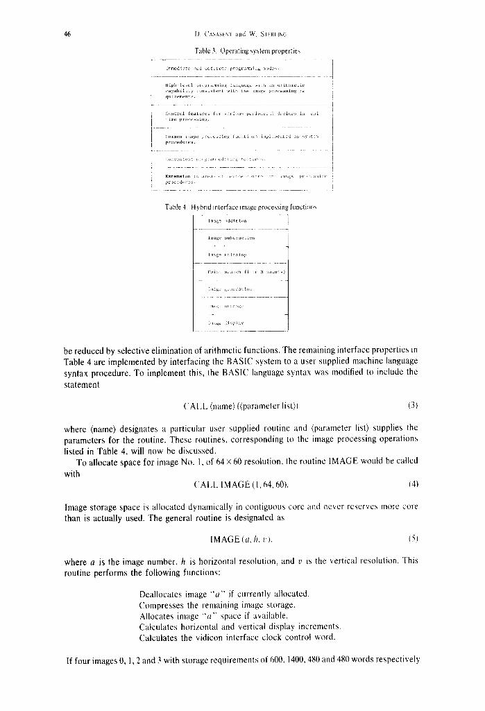
8. SOFTWARE SUPPORT
To fully utilize the real-time capability of the optical/digital interface and to provide control for the remainder of the system, a comprehensive and extensible operating system is needed. The properties of this operating system are listed in Table 3. The most common image processing functions used in the hybrid processor are listed in Table 4. The present implementation provides for 12K of core, in which the operating system, system procedures, user code, and image storage space must all be contained. The storage required for a binary-digitized image varies from eight words for an 8 x 8 element resolution image to 1440 words for a 96 x 240 element resolution image. The memory management scheme must permit this flexibility in the number of images concurrently stored.
The DEC single user BASIC system/16] was chosen to implement the operating system. It provides many of the features in Table 3. It is a high-level language with extensive arithmetic capability and can be operated in an intermediate or deferred programming mode. It also offers convenient editing features and requires a maximum of only 4K of core. This storage space can
46 1). CASASENT and W. SrERIIN(i
Table 3. Operating system properties
immedia te and d e f e r r e d prograrrm~ing modes .
I f i g h - i e ~ e l prc, g t m m n i n g l a n g u a g e ~ i t h m ~ r t t h m e t ic c a p a b i l i t y c c m s i s ~ e n t w i t h t h e image p t t ? c e s s i n g l~
quirement s. I . . . . . . . . . . . . . . . . . . . . . . . . . . .
C o n t r o l f e a t u r e s ~or v~ci , )u~ p e J i p t l e t ~] d e , ' f c e s in : e ~ i t i m e p r o c e s s i n g .
{;Oll~On image p r o c e s s i n g ir[Jnc[[~?tl~ i n l ; l e m e n t e d as s~,'~,ten~ p r o c e d u r e s ,
~Jonvel~Jen[ !E ,g~;lll c , ] i L J n g t c ~ c ~ , . ; .
Table 4, Hybrid interface image processing functiong
Image a d d i t i~n
image s u b c r a c t i u n
Image t h i n n i n g
F o i n t s e a r c h ( ! t c N p o i n t s )
[ i~lge s n e r a t ion
:mage s ~ c:r:tg,~
rt~l tge !i.~p I av
be reduced by selective elimination of arithmetic functions. The remaining interface properties in Table 4 are implemented by interfacing the BASIC system to a user supplied machine language syntax procedure. To implement this, the BASIC language syntax was modified to include the statement
CAM, (name) ((parameter list)) (3)
where (name) designates a particular user supplied routine and (parameter list) supplies the parameters for the routine. These routines, corresponding to the image processing operations listed in Table 4, will now be discussed.
To allocate space for image No. 1, of 64 × 60 resolution, the routine IMAGE would be called with
CALL IMAGE (I, 64, 60). (4)
Image storage space is allocated dynamically in contiguous core and never reserves more core than is actually used. The general routine is designated as
IMAGE (a, h, v ), (5)
where a is the image number, h is horizontal resolution, and v is the vertical resolution. This routine performs the following functions:
Deallocates image "a" if currently allocated. Compresses the remaining image storage. Allocates image "a" space if available. Calculates horizontal and vertical display increments. Calculates the vidicon interface clock control word.
If four images 0, 1,2 and 3 with storage requirements of 600, 1400, 481) and 480 words respectively
Digital analysis of optical transforms and correlations
are successively stored, 3000 words of memory are allocated. The statement
47
CALL IMAGE (2, 0, 0) (6)
will delete stored image No. 2. If this statement is followed by
CALL IMAGE (1, 96, 120), (7)
this causes the resolution of image 1 to be decreased from 96 × 240 (or 1440 words of memory) to 96 x 120 (or 720 words of memory).
The routines ADD (a, b, c) and SUB (a, b, c) enable two images " a " and "b" to be added or subtracted, where the destination image is "c". The routine SEARCH (a, b, c) locates the positions of a number "b" of "1" bits in a binary-digitized image "a" . The extracted coordinate positions are stored in array "c" where they can be examined.
The routines STORE (a) and LOAD (a) cause a binary-digitzed image to be punched on paper tape or loaded into core from paper tape respectively, where " a ' " is the image. The routine DISP (a, n) displays a binary-digitized image " a " on a CRT with n refresh scans. The routine VIDEO (a, t) by which the control words for the optical/digital interface are calculated and the digitization process on image " a " with threshold " t " is initiated has been described in the RTM hardware subroutine Ksub(INTERFACE). This comprises the digital interface and control section of the interface diagram of Fig. 2.
The routine GEN (a, i,/, b) is used to create "a" , a binary-digitized image. This is done by iteratively specifying a coordinate position (i, j) and the corresponding bit value "b". Space for this image must be allocated prior to execution of GEN.
The routine THIN (a) reduces the bit pattern in a binary-digitized image "a" to either a skeleton or a single point. This is necessary in cases in which a lower threshold is used with a wider resultant correlation peak and when the center of this peak must accurately be known. Examples of this in radar processing and in text and image correlation are available. This thinning is implemented by a combination of point searching and iterative technqiues. In particular, a set of N connected picture elements with coordinates (x,, y,), where i = 1 . . . . . N, are reduced to one element with coordinates ($, y), where
(x, Y) = (INT [ 1 ~ x~], INT [ 1 ~ Y,]). (8)
The operator INT truncates each coordinate value to the next lower integer. A recursive technique locates all connected picture elements once any element in this cluster is located.
9. EXPERIMENTAL RESULTS
Examples of these various interface operations, their use in a hybrid optical/digital processor in display and analysis and in digital feedback control of the optical processor, have been presented in previous papers. The purpose of this paper was to describe the digital hardware and implementation of the interface.
In optically processed radar data, the coordinates of this first-order fringe term in the transform plane provides data on the target's location or speed[ll, 12]. To insure that the first-order terms (especially those of lower peak intensity) are located for all targets, the lowest threshold level (that prevents assignment of the binary value " l " to secondary terms) is used. The more intense terms then produce a cluster of " l"s and the thinning routine is necessary to extract the central coordinate of this cluster.
In the case of area correlations using synthetic aperture radar maps, it was found[5/that the threshold could be varied over l0 or 11 orders without changing the digitally computed coordinates of the center of the cluster. In the case of radar processing, the entire system (KD2PO4 input transducer, optical system and interface) were found to be linear within 0.5% over the full 30 ° beam width of the phased array radar system used. The ability of all parts of the system (transducer, optical system and interface) to operate compatibly and in real time in area

41g I). (",ses~xl and W. SII-RI I'-,(i
correlation[g/, missile guidance[SI, reconnaisance, text correlation[9] and radar data processing[10, I1] has been demonstrated as is documented elsewhere.
Although the interface is intended to analyze and process the contents of transform and correlation planes, it can also be used to digitize coordinate images. Figure 9 is a binary-digitized image formed on the vidicon and fed into the optical/digital interface and PDP-11/15 in real time at 30 frames/see. While the system is not intended for such use. the output is indicative of the system's operation and resolution.
The present horizontal resolution ot the interface is imposed by the RTM bus system, which limits execution of Kmacro (ACCEPT VIDEO WORD) to 6 times every horizontal line scan (50/.,sec). This limits the transfer rate to (~ data words every 50/a.sec. The individual delay times for each bus operation [ 171 limit the worst case time for execution of Kmacro (ACCEPT VIDEO WORD) and return to its entry point to 9.0/~sec. The built-in time delays for the memory fetch operations and the arithmetic operations could be reduced, thus increasing horizontal resolution to 128 elements.
It should be emphasized that the modular design concept (using the RTM's) has produced an operational hybrid processor at a reasonable price and in a quite short time. The system's present resolution has been shown [5] to be over twice what is required for area correlation on synthetic aperature radar images and in text correlation. The interface resolution required in radar data processing[ll, 12] has been shown to be within the limits of most existing array antennas.
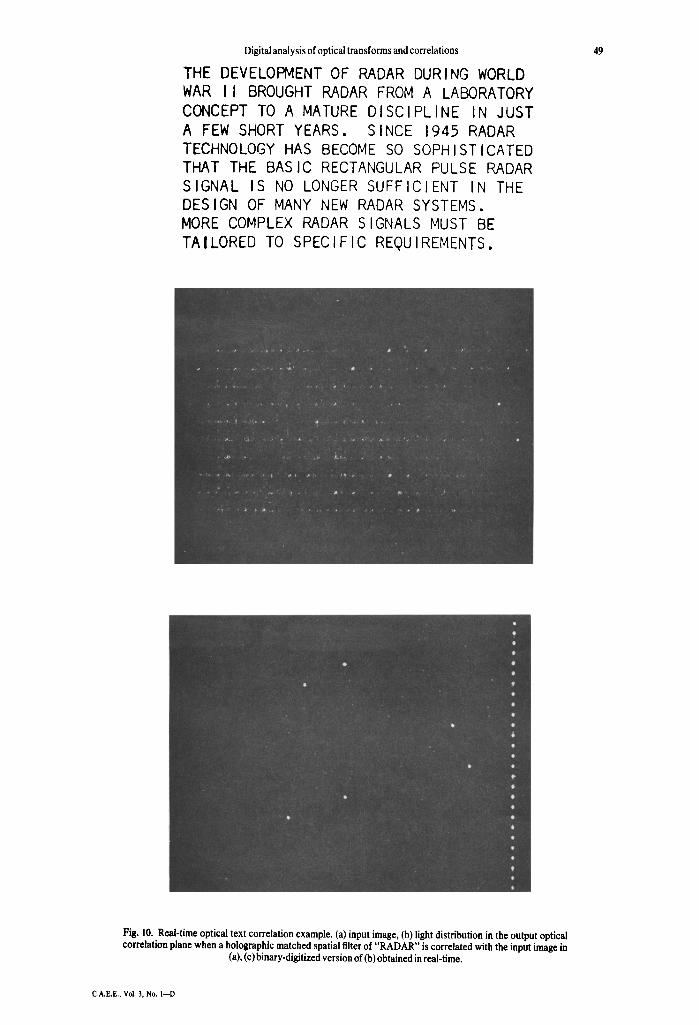
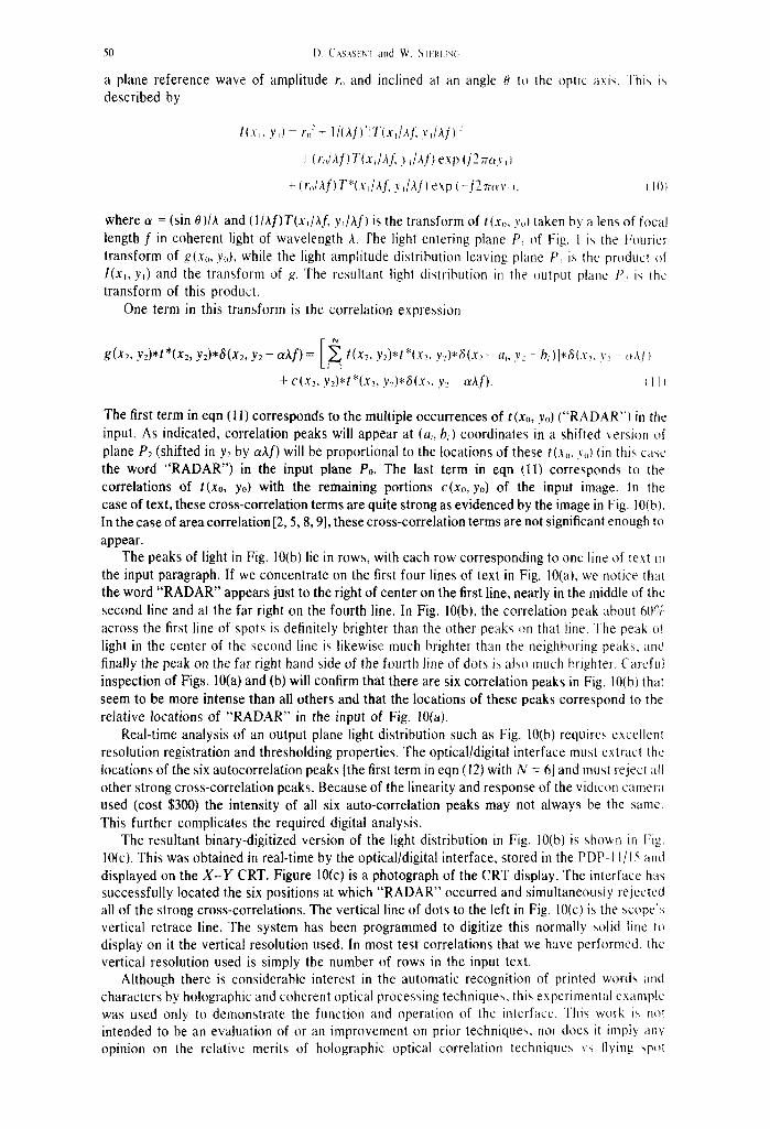
A simple optical data processing example that is more indicative of the system's intended function is shown in Fig. 10. The image in Fig. 10(a) was placed in the input plane P,, of an optical data processor (Fig. lI. A Fourier transform hologram (a matched spatial filter) of the word "RADAR" was placed in the transform plane P,. The light distribution in Fig. 10b is the resultant pattern that appears in the output correlation plane P, of Fig. 1.
The operations inw~tved in this example can be mathematically described by expressing the input image (Fig. 10al is:
,~'(-~ ,, 3 , ) : c(v,, v,,); ~, t(x,,, y,,>~;(x., a.v.. h,) r I
I9)
where t(x,,, yo) represents the input data Iin this case the word "RADAR") whose locations are to be determined. ]'he summation accounts for tile fact that N multiple occurrences of t(x,,, Yo) are possible (in this case N :: 6), while the delta function in eqn (101 shifts t(x,,, y,,) to its N relative locations (a~. h~) in the input image. The term c(x,,, y,,) corresponds to the remaining portion of the input image.
The holographic matched spatial filter for the word "RADAR" denoted by t(x,. yo) and placed in plane P, of Fig. I is the magnitude squared of the sum of the Fourier transform of t(xo, y,,) and
Fig. 9. '1 ypical binary-digitized coordinate hnage obtained m real-time on the hybrid proces'~or.
Digital analysis of optical transforms and correlations
THE DEVELOPMENT OF RADAR DURING WORLD WAR II BROUGHT RADAR FROM A LABORATORY CONCEPT TO A MATURE DISCIPLINE IN JUST A FEW SHORT YEARS. SINCE 1945 RADAR TECHNOLOGY HAS BECOME SO SOPHISTICATED THAT THE BASIC RECTANGULAR PULSE RADAR SIGNAL IS NO LONGER SUFFICIENT IN THE DESIGN OF MANY NEW RADAR SYSTEMS. MORE COMPLEX RADAR SIGNALS MUST BE TAILORED TO SPECIFIC REQUIREMENTS.
49
Fig. 10. Real-time optical text correlation example. (a) input image, (b) light distribution in the output optical correlation plane when a holographic matched spatial filter of "RADAR" is correlated with the input image in
(a), (c) binary-digitized version of (b) obtained in real-time.
C.A.E.E., Vol. 3, No. 1--D
50 I). (',~s~s~yt and W. SHRI r,a;
a plane reference wave of amplitude r,, and inclined at an angle 0 to lhe optic axis. This is described by
l(x,, y , ) - r,,:-~ II(af)'-IT(x,/a]~ y,/Af)l ~
l- (r,,/Af) T(x,/kf. y,/aJ) ex p (j 2 7my, )
~- (r,,/af)T*(x,/af, y ,~a f) exp (- j2 rr~y, i. I~)~
where a = (sin 0)/A and (l/Af)T(x./Af, ydAf) is the transform of t(xo, y,) taken by a lens of focal length f in coherent light of wavelength a. The light entering plane P, of Fig. I is the Fourier transform of g(x., yo), while the light amplitude distribution leaving plane P, is the product of l(x~, y,) and the transform of g. The resultant light distribution in the output plane P, is the transform of this product.
One term in this transform is the correlation expression
g(x2, y2)*t*(x2, y2)*a(x2, Y 2 - a a f ) = t(x2, y~)*t*(x> ye)*a(x . -a , ,y : -b , ) l*a(x> y, (,~]i
+ c(x,, y,)*t*(x~, y:)*a(x> y~_ - o~af). I III
The first term in eqn (! 1) corresponds to the multiple occurrences of t(Xo, yo) ("RADAR") in the input. As indicated, correlation peaks will appear at (a,, b,) coordinates in a shifted version of plane P2 (shifted in y2 by aAf) will be proportional to the locations of these t(x,, y,,) tin this case the word "RADAR") in the input plane Po. The last term in eqn (11) corresponds to the correlations of t(Xo, yo) with the remaining portions C(xo, yo) of the input image. In the case of text, these cross-correlation terms are quite strong as evidenced by the image in Fig. 10(b). In the case of area correlation [2, 5, 8, 9], these cross-correlation terms are not significant enough to appear.
The peaks of light in Fig. 10(b) lie in rows, with each row corresponding to one line of text in the input paragraph. If we concentrate on the first four lines of text in Fig. 10(a), we notice that the word "RADAR" appears just to the right of center on the first line, nearly in the middle of the second line and at the far right on the fourth line. In Fig. 10(b), the correlation peak about 6()5:~ across the first line of spots is definitely brighter than the other peaks on that line. The peak of light in the center of the second line is likewise much brighter than the neighboring peaks, and finally the peak on the far right hand side of the fourth line of dots is also much brighter. Careful inspection of Figs. 10(a) and (b) will confirm that there are six correlation peaks in Fig. 10(b) that seem to be more intense than all others and that the locations of these peaks correspond to the relative locations of "RADAR" in the input of Fig. 10(a).
Real-time analysis of an output plane light distribution such as Fig. 10(b) requires excellent resolution registration and thresholding properties. The optical/digital interface must extract the locations of the six autocorrelation peaks [the first term in eqn (12) with N : 6] and must rejec~ all other strong cross-correlation peaks. Because of the linearity and response of the vidicon camera used (cost $300) the intensity of all six auto-correlation peaks may not always be the same. This further complicates the required digital analysis.
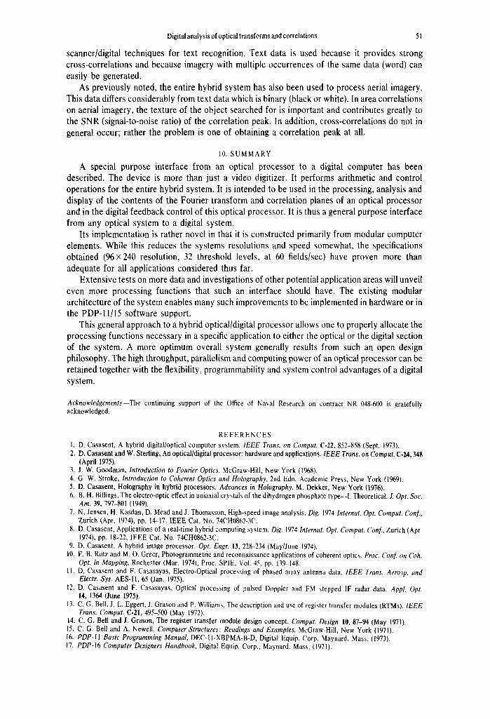
The resultant binary-digitized version of the light distribution in Fig. 10(b) is shown in Fig. 10(c), This was obtained in real-time by the optical/digital interface, stored in the PDP-11/I 5 and displayed on the X - Y CRT. Figure 10(c) is a photograph of the CRT display. The interface has successfully located the six positions at which "RADAR" occurred and simultaneously rejected all of the strong cross-correlations. The vertical line of dots to the left in Fig. 10(c) is the scopc'~ vertical retrace line. The system has been programmed to digitize this normally solid line to display on it the vertical resolution used. In most test correlations that we have performed, the vertical resolution used is simply the number of rows in the input text.
Although there is considerable interest in the automatic recognition of printed words and characters by holographic and coherent optical processing techniques, this experimental example was used only to demonstrate the function and operation of the interface. ]'his work is nol intended to be an evaluation of or an improvement on prior techniques, nor does it imply any opinion on the relative merits of holographic optical correlation techniques vs flying sp~l
Digital analysis of optical transforms and correlations 5l
scanner/digital techniques for text recognition. Text data is used because it provides strong cross-correlations and because imagery with multiple occurrences of the same data (word) can easily be generated.
As previously noted, the entire hybrid system has also been used to process aerial imagery. This data differs considerably from text data which is binary (black or white). In area correlations on aerial imagery, the texture of the object searched for is important and contributes greatly to the SNR (signal-to-noise ratio) of the correlation peak. In addition, cross-correlations do not in general occur; rather the problem is one of obtaining a correlation peak at all.
10. SUMMARY
A special purpose interface from an optical processor to a digital computer has been described. The device is more than just a video digitizer. It performs arithmetic and control operations for the entire hybrid system. It is intended to be used in the processing, analysis and display of the contents of the Fourier transform and correlation planes of an optical processor and in the digital feedback control of this optical processor. It is thus a general purpose interface from any optical system to a digital system.
Its implementation is rather novel in that it is constructed primarily from modular computer elements. While this reduces the systems resolutions and speed somewhat, the specifications obtained (96× 240 resolution, 32 threshold levels, at 60 fields/sec) have proven more than adequate for all applications considered thus far.
Extensive tests on more data and investigations of other potential application areas will unveil even more processing functions that such an interface should have. The existing modular architecture of the system enables many such improvements to be implemented in hardware or in the PDP-I1/15 software support.
This general approach to a hybrid optical/digital processor allows one to properly allocate the processing functions necessary in a specific application to either the optical or the digital section of the system. A more optimum overall system generally results from such an open design philosophy. The high throughput, parallelism and computing power of an optical processor can be retained together with the flexibility, programmability and system control advantages of a digital system.
Acknowledgements--The continuing support of the Otfice of Naval Research on contract NR 048-600 is gratefully acknowledged.
R E F E R E N C E S I. D. Casasent, A hybrid digital/optical computer system. IEEE Trans. on Comput. C-22, 852-858 (Sept. 1973). 2. D. Casasent and W. Sterling, An optical/digital processor: hardware and applications. IEEE Trans. on Comput. C-24, 348
(April 1975). 3. J. W. Goodman, Introduction to Fourier Optics. McGraw-Hill, New York (1968). 4. G. W. Stroke, Introduction to Coherent Optics and Holography, 2nd Edn. Academic Press, New York (1%9). 5. D. Casasent, Holography in hybrid processors. Advances in Holography. M. Dekker, New York (1976). 6. B. H. Billings, The electro-optic effect in uniaxial crystals of the dihydrogen phosphate type--I. Theoretical. J. Opt. Soc.
Am. 39, 797-801 (1949). 7. N. Jensen, H. Kasdan, D. Mead and J. Thomasson, High-speed image analysis. Dig. 1974 lnternat. Opt, Comput. Con[.,
Zurich (Apr. 1974), pp. 14-17. IEEE Cat. No. 74CH0862-3C. 8. D. Casasent, Applications of a real-time hybrid computing system. Dig. 1974 lnternat. Opt. Comput. Con[., Zurich (Apr.
1974), pp. 18-22, IEEE Cat. No. 74CH0862-3C. 9. D. Casasent, A hybrid image processor. Opt. Engr. 13, 228-234 (May/June 1974).
10. F. B. Rotz and M. O. Greet, Photogrammetric and reconnaissance applications of coherent optics. Proc. Con[. on Coh. Opt. in Mapping, Rochester (Mar. 1974), Proc. SPIE, Vol. 45, pp. 139-148.
11. D. Casasent and F. Casasayas, Electro-Optical processing of phased array antenna data. IEEE Trans. Aerosp. and Electr. Sys. AES-11, 65 (Jan. 1975),
12. D. Casasent and F. Casasayas, Optical processing of pulsed Doppler and FM stepped IF radar data. AppL Opt. 14, 1364 (June 1975).
13. C. G. Bell, J. L. Eggert, J. Grason and P. Williams, The description and use of register transfer modules (RTMs). IEEE Trans. Comput. C-21,495-500 (May 1972).
14. C. G. Bell and J. Grason, The register transfer module design concept. Comput. Design 10, 87-94 (May 1971). 15. C. G. Bell and A. Newell, Computer Structures: Readings and Examples. McGraw-Hill, New York (1971). 16. PDP-I1 Basic Programming Manual, DEC-II-XBPMA-B-D, Digital Equip. Corp. Maynard, Mass. (1973). 17. PDP-16 Computer Designers Handbook, Digital Equip. Corp., Maynard, Mass. (1971).