Embed Size (px)
Citation preview
Digital Electronics 1 (ET181)
Laboratory Manual (Where theory meets practice)
Written by
Asst. Professor William E. Hunt III Mohawk Valley Community College
Utica, NY
Version 1.5
March 21, 2018

Digital Electronic 1 Laboratory Manual
This page is intentionally left blank
Page 2 of 111

Digital Electronic 1 Laboratory Manual
This Laboratory Manual by William E. Hunt III is copyrighted under the terms of a
Creative Commons license:
This work is licensed under the Creative Commons Attribution-NonCommercial-ShareAlike 4.0 International License.
To view a copy of this license, visit http://creativecommons.org/licenses/by-nc-sa/4.0/.
Page 3 of 111

Digital Electronic 1 Laboratory Manual
~ Dedication ~
To my Father, William Edward Hunt Jr., an Electrical Engineer, the ultimate role model, who provided me with the opportunity to explore electronics in my youth and encouraged a lifelong passion to learn and share the knowledge.
~ Acknowledgements ~
This work would not have been possible without the financial support of Mohawk Valley Community College and the technical support of my colleagues, Professor James Fiore and Professor Robert Decker.
I am grateful to all my students, who have inspired and challenged me to be better every day. Nothing brings more energy to a project than enthusiastic and demanding students. As I introduce this manual in the laboratory sessions, I will continue to receive student feedback and make improvements to this manual.
Finally, it is with my deepest appreciation, I would like to acknowledge the unconditional support and love of my wife and four daughters. They have allowed me to research, develop, test and write during my “free” time. This manual would not have been possible without their support.
Page 4 of 111
Digital Electronic 1 Laboratory Manual
Table of Contents
Introduction ...................................................................................................
Safety ...........................................................................................................
Experiment 1 - Logic Trainer Familiarization 1 .............................................
Experiment 2 - Logic Trainer Familiarization 2 .............................................
Experiment 3 - Breadboards and Building Digital Circuits ............................
Experiment 4 – AND, OR and NOT Gates ...................................................
Experiment 5 - Basic Combinational Logic & Gates with Many Inputs .........
Experiment 6 - DeMorgan’s Theorem ..........................................................
Experiment 7 - NAND Gates and the Universality of NAND Gates ...............
Experiment 8/9 - BCD Detector Project with Karnaugh Maps.......................
Experiment 10 – S-R and D Latches and J-K Flip Flops ..............................
Experiment 11 – Shift Registers ...................................................................
Experiment 12 – Half and Full Adders ..........................................................
Experiment 13 - 3-Bit Adder Project .............................................................
Experiment 14 – Design a Asynchronous Counter .......................................
Appendix A – Experiment Grading Sheet .....................................................
Page 5 of 111
Digital Electronic 1 Laboratory Manual
Introduction
There are two hours assigned weekly to the laboratory session of Digital Electronic 1. Attendance is mandatory and a passing grade in the laboratory component is required to pass the course. Below are some general guidelines to be successful with each experiment. • Read over the experiment before arriving. • Sketch out a logic diagram or use MultiSim (required for some experiments)
prior to building the circuit. Instructor signature may be needed • For full credit do any prelab work and bring to the laboratory session. • Careful read and follow all instructions. • Review the logic diagram and verify all pin numbers are assigned. • Review and use the “How to use a breadboard” document. • Be sure to get the instructor’s signature on every required element in the
experiment. • Ask questions for clarification.
Page 6 of 111

Digital Electronic 1 Laboratory Manual
Safety First
The experiments in this lab manual are designed for low voltage which minimizes the electrical shock hazard, but it only takes several milliamperes of current to cause a harmful electrical shock. Safety must always be first.
Below are several general safety rules for all digital experiments and activities in the laboratory.
1. Avoid direct contact with any power source. Turn off all power sources when not needed.
2. When hooking up a circuit, connect to the power source last, while power is off.
3. Before making changes in a circuit, turn off or disconnect the power first.
4. Never work alone in the laboratory. Use the buddy system.
5. When changing a powered up connection, use only one hand. Never touch two points in the circuit that are at different voltages.
6. Know that the circuit and connections are correct before applying power to the circuit. if needed have the instructor review the circuit before applying power.
7. Know the location of the emergency power-off switch at each bench.
8. Keep the work area around the circuit and test equipment neat and free of clutter.
9. Remove all jewelry that can be seen before working on any experiment.
Follow these rules and see the instructor with any questions.
Page 7 of 111

Digital Electronic 1 Laboratory Manual
Experiment 1 Logic Trainer Familiarization 1
Objectives:
• To become familiar with the Logic trainer • To perform DC Measurements on Signal Sources
Text References:
Tocci Chapter 1 Sections 1-3 through 1-6
Components Needed:
None
Equipment Needed:
• Knight electronics ML-2001 logic trainer • Digital multimeter (DMM) • Logic probe
Discussion:
The digital logic trainer used in this lab includes a number of features to support the design and fabrication of logic circuits in the lab. The main features include:
• Fixed and variable positive and negative DC power supplies
• Fixed 60 Hz AC power supply
• Pulse generator with continuously variable pulse widths from 100 nSec to 10 mSec and repetition rates from 1 μSec to 100 mSec
• Pulse duty cycles from 0 – 100%
• Pulse position and width modulation inputs
• Sweep generator Function with variable period from 1 mSec to 1 second
• Function generator with sine, square, and triangular output from 1 Hz to 1 MHz with logic level and variable DC offset output.
• 8 - Logic level switches
Page 8 of 111
Digital Electronic 1 Laboratory Manual
• 2 – Momentary pulse switches with logic level normally HIGH and normally LOW outputs
• 8 – Logic level LED indicators
In this lab, you will investigate some of these features and measure DC output levels from the sources present.
Procedure:
1. Unpacking and Setting Up/Initial Voltage Measurements
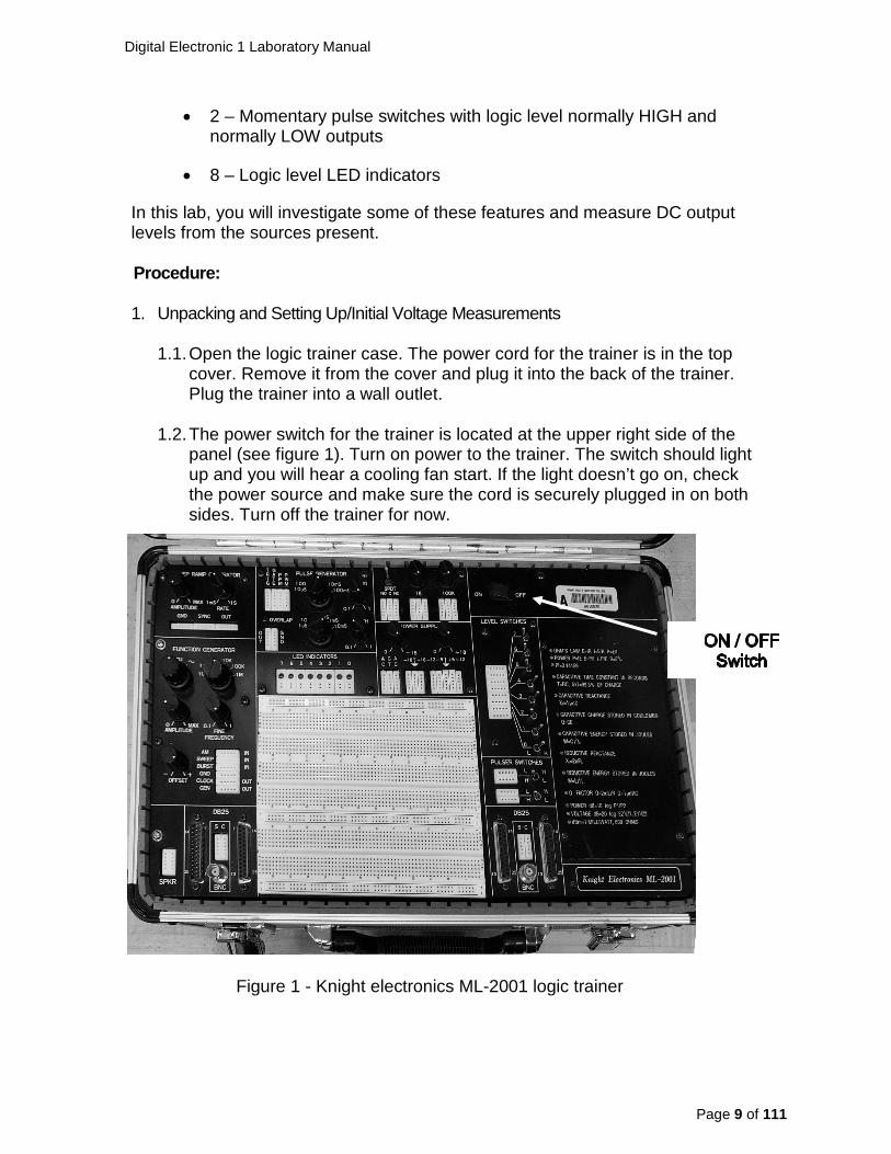
1.1. Open the logic trainer case. The power cord for the trainer is in the top cover. Remove it from the cover and plug it into the back of the trainer. Plug the trainer into a wall outlet.
1.2. The power switch for the trainer is located at the upper right side of the panel (see figure 1). Turn on power to the trainer. The switch should light up and you will hear a cooling fan start. If the light doesn’t go on, check the power source and make sure the cord is securely plugged in on both sides. Turn off the trainer for now.
Figure 1 - Knight electronics ML-2001 logic trainer
Page 9 of 111

Digital Electronic 1 Laboratory Manual
2. Measurement of Power Supply Voltages. Figure 2 below shows the power supply section of the logic trainer. All measurements should be recorded to a tenth of a volt.
Figure 2 – Power Supply Section
2.1. On the bottom right, 5 parallel banks of 5 connection points each are labeled (from left to right) -12, -5, ground (symbol), + 5, and +12. These points are for different FIXED voltage outputs. The knob above these points does NOT affect these voltages, and all levels are referenced to the center, or ground connection.
2.2. Set your DMM for DC voltage in the 20V range (approximately) and insert a short wire into the +5 and another short wire into one of the ground points on the digital trainer. Connect these leads to the common and +V inputs of your DMM. Turn on the digital trainer and measure the DC voltage, noting its polarity.
V @ +5 point = ________ VDC (record voltage to a tenth of a volt)
Digital logic devices often operate within a very narrow range of voltages (typically within 10% or less), and the reading should be very close to 5V. If it is not, check your DMM to be sure you are on the right range and if you cannot get the correct reading, contact your instructor for assistance.
Page 10 of 111

Digital Electronic 1 Laboratory Manual
2.3. A Logic Probe does not have batteries so it needs to be connected to power (+5 and ground) before making measuring the logical states (Boolean 0 or 1) of a circuit. Remove the DMM connections but leave the two wires inserted into the terminals. Connect the black lead of the Logic Probe to the wire inserted in the ground terminal and the red lead of the Logic Probe to the wire inserted in the +5 terminal.
2.4. Insert another short wire into one of the remaining +5 holes and a second short wire into one of the remaining ground points on the digital trainer. Connect the measuring point of the Logic Probe to the +5 wire and record the reading on the Logic Probe.
Logic state @ +5 point = ________
2.5. Connect the measuring point of the Logic Probe to the ground wire and record the reading on the Logic Probe.
Logic state @ ground point = ________
2.6. Leave the wires that are currently in the ground point on the trainer in place. Remove one of the wires from the +5 point and move it to the +12 point. Measure this voltage and record it below. Note the polarity as well. The black lead should be connected to the common input on your DMM and to the ground connection point on the trainer.
V @+12 point = _______ VDC (record voltage to a tenth of a volt)
2.7. Do NOT use the Logic Probe on the +12 terminal. Move the lead from the +12 point to the -5 point and record the voltage and polarity below. Do the same for the -12 point and record its amplitude and polarity.
V @ -5 point = _______ VDC (record voltage to a tenth of a volt)
V @ -12 point = _______ VDC (record voltage to a tenth of a volt)
Page 11 of 111

Digital Electronic 1 Laboratory Manual
All readings should be within 10% of their marked voltages. Some interface devices in digital logic require both positive and negative polarity power supplies, and in those circuits, it is common to see a 0V ground reference. Turn off the trainer for the next measurement.
3. Variable Voltage Supply
3.1. Looking to the center of figure 2. Three parallel banks of 5 connections each are present. These are marked -18, ground (symbol), and +18. These connections are for the VARIABLE positive and negative power supplies provided in the logic trainer. The two knobs above these points are used to adjust the magnitude of these voltages, and the adjustments are independent of one another. Remove one of the ground wires from the FIXED power supply ground point on the trainer (keep it connected to your DMM) and insert it into the ground point on this supply. Remove the other wire from the -12 point and connect it to the +18 point on this supply and to the positive lead of your DMM. Turn the right knob (marked 0 +18) completely counter-clockwise. Turn on the logic trainer and measure the output voltage. It may be very close to 0V.
Vmin (+18) = _______ VDC (record voltage to a tenth of a volt)
3.2. Rotate the knob fully clockwise and read the output voltage
Vmax (+18) = _______ VDC (record voltage to a tenth of a volt)
3.3. Rotate the knob marked 0 -18. Note that it has no effect on the positive supply voltage.
3.4. Remove the lead from the +18 point and insert it into the -18 point. Repeat the steps above for the -18V supply and verify the MAGNITUDE of the levels present. Remember to include the polarity of the voltage!
Vmin (-18) = _______ VDC (fully counter-clockwise)
Vmax (-18) = _______ VDC (fully clockwise).
Page 12 of 111
Digital Electronic 1 Laboratory Manual
Some logic circuits operate at voltages other than 5V and many linear/analog parts require both positive and negative voltages for their operation. These power supplies can accommodate a variety of needs.
3.5. Turn the logic trainer off. Move the negative lead of your DMM from the VARIABLE voltage supply ground point (which is NOT common with the fixed voltage supplies) to the ground point of the FIXED voltage supply for the next part of this exercise.
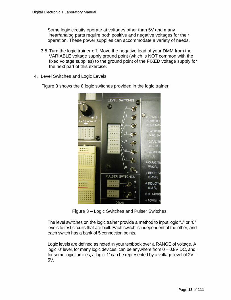
4. Level Switches and Logic Levels
Figure 3 shows the 8 logic switches provided in the logic trainer.
Figure 3 – Logic Switches and Pulser Switches
The level switches on the logic trainer provide a method to input logic “1” or “0” levels to test circuits that are built. Each switch is independent of the other, and each switch has a bank of 5 connection points.
Logic levels are defined as noted in your textbook over a RANGE of voltage. A logic ‘0’ level, for many logic devices, can be anywhere from 0 – 0.8V DC, and, for some logic families, a logic ‘1’ can be represented by a voltage level of 2V – 5V.
Page 13 of 111

Digital Electronic 1 Laboratory Manual
4.1. Measure the logic levels from these logic switches using your DMM as follows:
• Be sure the negative lead of the DMM is connected to the ground of the FIXED power supply.
• Connect the positive lead of the DMM to the connection point for switch 0.
• Turn on the Logic trainer and put the switch into the L (low) position. Read the DC voltage.
• Move the switch to the H (high) position. Read the DC voltage.
• Record these voltages below
V(low) = ________ V V(high) = _______ V
Are these voltages within the range mentioned above? _______
4.2. Repeat this measurement with the Logic Probe and record the results below.
Logic state @ Level Switch LOW = ________
Logic state @ Level Switch HIGH = ________
4.3. Repeat this for other switches in the group. The logic levels should be the same for all 8 switches. If they are not within 10 % of each other, contact your instructor for assistance.
5. Pulser Switches
5.1. The two pulser switches (lower part of figure 3) are intended to provide momentary logic level changes when the switch is pressed. The switches have a spring-return device, so they will not remain in right-most position when released. Some logic circuits require a “positive-going” transition (PGT) which means when activated, the switch output goes from a logic ‘0’ to a logic ‘1’ level and returns to the ‘0’ level when released. Draw a single 5V pulse signal and label the PGT.
Page 14 of 111
Digital Electronic 1 Laboratory Manual
5V
0V
5.2. Others require a ”negative-going” transition (NGT). In that case, the output goes to ‘0’ or LOW when activated and returns to the ‘1’ or HIGH level when released. Draw a single 5V pulse signal and label the NGT.
5V
0V
5.3. For convenience, both options are provided in these switches. Note that there are two rows of connecting points for each switch. The upper row is marked L H (LOW to HIGH) and the lower row is marked H L (HIGH to LOW). Connect your DMM positive lead to the L H input and measure the voltage (leave the negative lead on the ground point of the power supply). Record the voltage when the switch is in each position below. Remember, the switch will spring back to the left when released, and the level will change back to its original value.
Voltage Level (L H Row)
Released _______ V Activated _______ V
Voltage Level (H L Row)
Released _______ V Activated _______ V
These levels should be equal and opposite for both positions and for both switches.
Instructor initials:
Page 15 of 111

Digital Electronic 1 Laboratory Manual
6. LED Indicators and Logic Levels
The Logic trainer includes 8 LED indicators to monitor circuit outputs. These indicators respond to logic levels and will only go on or off if the voltage level at the input is a valid logic level (typically less than 0.8V for logic ‘0’ which corresponds to OFF or greater than 2.0V for a logic ‘1’ or ON indication. Since the indicators use the power supply in the Logic trainer, the inputs do not require a separate ground and they can monitor logic levels by directly connecting them to the device output.
6.1. To test the logic indicator, connect a wire from one of the level switches to one of the LED indicator inputs. Switch the level between L and H and note the LED indicator output. You can also try this with the pulser switch outputs. Note that the L H switch output turns on the LED when the switch is activated but that it shuts off when released and the opposite occurs when the H L switch output is used.
Questions:
1. What voltage levels are commonly found at the outputs of the level switches on the Logic trainer for logic ‘0’ and logic ‘1’ levels?
2. What are the advantages of using a DMM rather than a Logic Probe?
3. What are the advantages of using the Logic Probe rather than a DDM?
Page 16 of 111

Digital Electronic 1 Laboratory Manual
4. A logic “1” or an ON condition is represented with what voltage level?
5. A logic “0” or OFF condition is represented with what voltage level?
6. Give two examples of an analog quantity.
7. Give two examples of a digital quantity.
8. Explain why computers are based on digital signals rather than analog signals?
Page 17 of 111

Digital Electronic 1 Laboratory Manual
Experiment 2 Logic Trainer Familiarization 2
Objectives:
• To become familiar with the Logic trainer • To perform AC Measurements on Signal Sources
Text References:
Tocci Chapter 1 Sections 1-3 through 1-6
Components Needed:
None
Equipment Needed:
• Knight electronics ML-2001 Logic trainer • Oscilloscope • Digital multimeter (DMM)
Discussion:
The digital Logic trainer used in this lab includes a number of features to support the design and fabrication of logic circuits in the lab. The main features include:
• Fixed and variable positive and negative DC power supplies
• Fixed 60 Hz AC power supply
• Pulse generator with continuously variable pulse widths from 100 nSec to 10 mSec and repetition rates from 1 μSec to 100 mSec
• Pulse duty cycles from 0 – 100%
• Pulse position and width modulation inputs
• Sweep generator Function with variable period from 1 mSec to 1 second
• Function generator with sine, square, and triangular output from 1 Hz to 1 MHz with logic level and variable DC offset output.
• 8 - Logic level switches
Page 18 of 111

Digital Electronic 1 Laboratory Manual
• 2 – Momentary pulse switches with logic level normally HIGH and normally LOW outputs
• 8 – Logic level LED indicators
In this lab, you will investigate some of these features and measure output levels from the AC sources present.
Procedure:
1. Signal Generators and Measurement of Logic Levels
The Logic trainer includes a variety of signal sources for use with digital and analog circuitry. The function generator is widely used in most experiments and will serve as an introduction both to the trainer features and to logic level waveforms.
Figure 4 shows the function generator section of the trainer. It can provide a sine, triangular, or square wave signal input to logic circuits or other devices in the range from 1 Hz (or 1 cycle per second) to approximately 1 MHz (or 1 million cycles per second). The Waveform knob at the upper left controls the wave shape. The Range switch at the right of this knob selects the range in Hz in decades and the Fine Frequency control below the range switch provides a method to adjust the range within the decade.
Figure 4 – Function Generator
Page 19 of 111

Digital Electronic 1 Laboratory Manual
As an example, if the range switch is set to 10, with the Fine Frequency fully counter-clockwise (near 0.1), the frequency is 10 * 0.1 = 1 Hz. With the Fine Frequency control fully clockwise, the frequency is approximately 10 Hz.
Digital circuitry does NOT respond well to signal inputs with long transition times between logic ‘0’ and logic ‘1’ levels, such as sinusoidal or trapezoidal waveforms. As a result, these waveforms are typically NOT used in digital designs. Rectangular waveforms including the square waves (waveforms where the ON time and OFF time are equal) are preferred.
Figure 5 – Two waveforms with long transition times versus the rectangular wave
As shown in Figure 5, digital inputs typically have their LOW logic level at zero volts DC and their HIGH logic level limited to the supply voltage used with the logic device (typically 5 VDC as seen in last week’s lab).
The output labeled CLOCK in this panel is used to provide a logic level pulse that is independent of the Amplitude and Offset control setting knobs on the function generator.
The GEN output provides a signal level whose amplitude and offset (midpoint of the waveform position with respect to 0V) can be adjusted using the Amplitude and Offset controls. This output is not commonly used in typical digital electronics labs.
The GND connection point is the common ground for all generator functions and should be connected to the power supply ground point when using this generator as a signal source.
Page 20 of 111

Digital Electronic 1 Laboratory Manual
We will not use the terminals labelled as AM IN, SWEEP IN or BURST IN.
1.1. Measurement of Amplitude and Frequency from the Clock Generator
The DMM will not accurately measure most AC voltages above anywhere from 100 – 100KHz depending on model and type, and most DMMs cannot measure non-sinusoidal waveforms accurately, so an oscilloscope is required. Take a moment to record the make, model, and serial number of the instrument at your lab station.
Oscilloscope Make (Manufacturer) ______________________________
Model ____________________________-_
Serial Number ______________________________
Since all oscilloscopes in the lab are the same make and model, the serial number information is useful in identifying a specific instrument, especially if there are problems or concerns about accuracy. Make a habit of recording this information in your lab reports!
Figure 6 – Horizontal Sweep
Page 21 of 111
Digital Electronic 1 Laboratory Manual
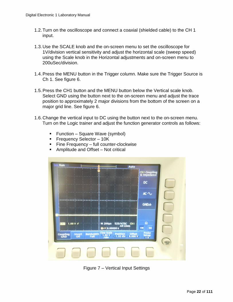
1.2. Turn on the oscilloscope and connect a coaxial (shielded cable) to the CH 1 input.
1.3. Use the SCALE knob and the on-screen menu to set the oscilloscope for 1V/division vertical sensitivity and adjust the horizontal scale (sweep speed) using the Scale knob in the Horizontal adjustments and on-screen menu to 200uSec/division.
1.4. Press the MENU button in the Trigger column. Make sure the Trigger Source is Ch 1. See figure 6.
1.5. Press the CH1 button and the MENU button below the Vertical scale knob. Select GND using the button next to the on-screen menu and adjust the trace position to approximately 2 major divisions from the bottom of the screen on a major grid line. See figure 6.
1.6. Change the vertical input to DC using the button next to the on-screen menu. Turn on the Logic trainer and adjust the function generator controls as follows:
Function – Square Wave (symbol) Frequency Selector – 10K Fine Frequency – full counter-clockwise Amplitude and Offset – Not critical
Figure 7 – Vertical Input Settings
Page 22 of 111

Digital Electronic 1 Laboratory Manual
1.7. Connect the cable to the CLOCK and GND points on the function generator. Observe the display on the oscilloscope. You may need to adjust the horizontal position to align the edge of the waveform with one of the major vertical grid lines.
1.8. Measure the AMPLITUDE of the waveform (peak to peak value) by counting the grid squares on the screen. Remember, each square is 1.0V. Is it close to 5V? Record your reading below.
Amplitude (p-p) _______ V
1.9. Note the position of the BOTTOM portion of the trace as compared to the GROUND level you set in step a. To verify the DC offset of the waveform, compare the position of that part of the trace to the ground position. For work with digital circuits, there should be little or no offset (e.g. the lowest level of the input waveform should be at 0 VDC.
Offset (V) _______ V
1.10. Measure the FREQUENCY of the waveform by counting the number of grid marks on the scope display. In order to measure frequency, you must count from one rising edge of the waveform to the next rising edge. Each grid square horizontally corresponds to 200 uSec, so add up the number of squares to get the period of the waveform. Remember that frequency = 1/period. Write down the period and then invert it to get the frequency. Record this information below.
Period = _____ grid squares * 200 uSec/Square = _______ uSec
Frequency = 1/Period = _________ Hz
1.11. Use graph paper to sketch the waveform. Observe the scale for both amplitude and timing of the waveform on your screen. Use grid lines and scaling to make the sketch large enough to read the frequency and amplitude accurately!
1.12. Adjust the Fine Frequency control on the logic trainer to about mid-scale. Measure the period and frequency of the waveform on the oscilloscope. Remember to use the Horizontal position control to move the waveform so you can align it to a major grid line. Record this information below.
Instructor initials:
Page 23 of 111
Digital Electronic 1 Laboratory Manual
Period = _____ grid squares * 200uSec/Square = _______ uSec
Frequency = 1/Period = _________ Hz
1.13. Adjust the Fine Frequency control on the logic trainer to the full clockwise position. The frequency will go up to the point where it will be difficult to measure on the oscilloscope. Change the Horizontal scale to 20 uSec/division and measure the period and frequency as above. Record this information below.
Period = _____ grid squares * 20uSec/Square = ________ uSec
Frequency = 1/Period = ________ Hz
2. Measurement of Amplitude and Frequency from the Function Generator
Although the function generator provides a wide range of frequencies for use, the exact frequency is difficult to set due to the variable nature of the components used and settings of the controls. The function generator GEN output provides a variable signal level that can be adjusted using the AMPLITUDE control. The DC offset of this waveform can be adjusted using the OFFSET control. Refer to figure 4. Adjust these controls as follows for the next measurement: Amplitude: Approximately ¼ (9:00 position) Offset: Approximately ½ (12:00 position)
2.1. Move the oscilloscope input wire from the CLOCK connection point to the GEN connection point on the logic trainer (see figure 4). DO NOT adjust the vertical position of the waveform on the oscilloscope.
2.2. Measure the amplitude of the waveform present. Record this information below.
Amplitude = ______ V
2.3. The DC offset is the difference between the level of the bottom of the waveform and your reference point, which should be at the second major division on the screen from the bottom. Using this as a reference, measure the DC offset and record it below. Remember to include the polarity!
DC Offset = ______ V
Page 24 of 111

Digital Electronic 1 Laboratory Manual
2.4. Adjust the DC offset control to get to your “zero-volt” reference point. Note that the amplitude of the waveform doesn’t change, but that the offset does.
Questions (show your work for all computation):
1) What is the frequency of a square wave signal with a period of 1.05 mSec?
2) What types of waveforms are difficult for digital logic circuits to work with? Explain why?
3) Which output of the function generator on the digital trainer is usually used when working with digital circuitry?
Page 25 of 111
Digital Electronic 1 Laboratory Manual
Experiment 3 Breadboards and Building Digital Circuits
Objectives:
• To become familiar the typical solderless breadboard or protoboard and its features • To understand the internal connections on a breadboard • To understand how to wire a simple digital circuit using a breadboard • To apply the binary, decimal and hexadecimal conversions
Text References: Instructor handout: “How to Use a Breadboard” Tocci Chapter 2 Sections 2-1 through 2-3
Components Needed:
1 Integrated Circuit ( type 7476)
Equipment Needed:
• Knight electronics ML-2001 logic trainer • Digital Multimeter (DMM) • Logic Probe
Discussion:
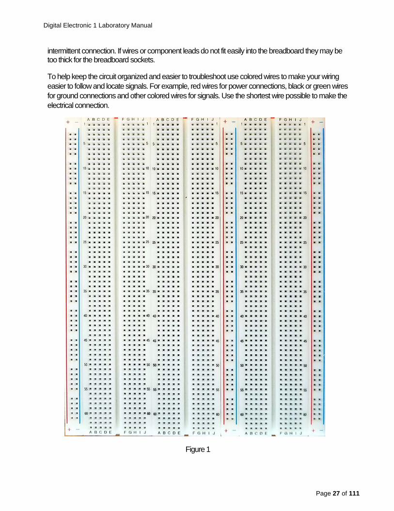
The breadboard is organized into rows (1, 2, 3, 4,…) and columns (A, B, C, D,…J) of electrical sockets. See Figure 1. Those rows and columns can be further subdivided into groups. The breadboards that are provided with the logic trainer have pairs of columns with + and – labels (usually between a red and blue lines). These are power rails or buses that are used to supply a common voltage (+5V or +12V) and a common ground to the circuits in the main part of the board. Good bus management will save you time and trouble with complicated circuits by simplifying circuit wiring and by removing unnecessary clutter. Clutter is your enemy in building circuits!
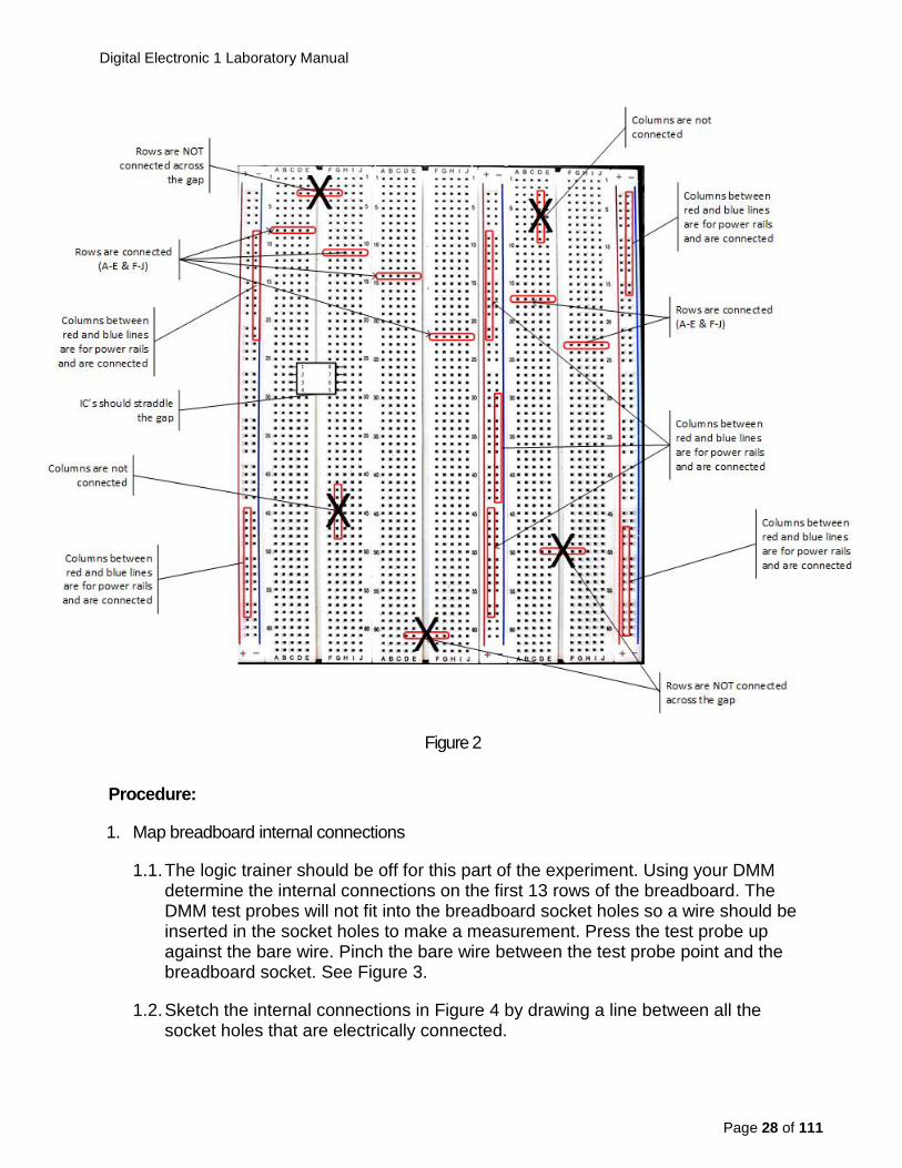
Between the power rails are groups of sockets that will be used to build the circuit and, within these groups of sockets, only the rows of sockets are electrically connected. See Figure 2. The two groups across the central gap are not connected. In other words, sockets A - E in a row are not connected to sockets F - J) in the same row. Look over Figure 2 and be sure to understand the connections between sockets.
To prevent damage to the breadboard sockets, use 22 gauge solid wire to make connections. Cut the wires to the correct length or use the precut wires. If needed strip about 1/2” of insulation from each end and push the bare wires into the breadboard sockets until they bottom out. Forcing wires or component leads into the board will damage the internal socket connections or make for an
Page 26 of 111
Digital Electronic 1 Laboratory Manual
intermittent connection. If wires or component leads do not fit easily into the breadboard they may be too thick for the breadboard sockets.
To help keep the circuit organized and easier to troubleshoot use colored wires to make your wiring easier to follow and locate signals. For example, red wires for power connections, black or green wires for ground connections and other colored wires for signals. Use the shortest wire possible to make the electrical connection.
Figure 1
Page 27 of 111
Digital Electronic 1 Laboratory Manual
Figure 2
Procedure:
1. Map breadboard internal connections
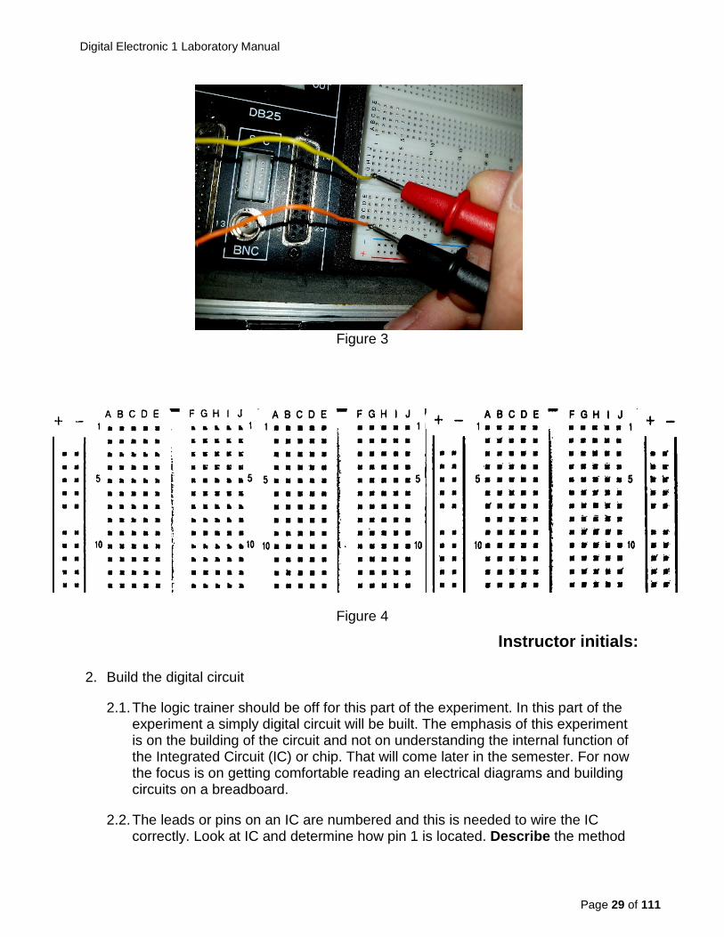
1.1. The logic trainer should be off for this part of the experiment. Using your DMM determine the internal connections on the first 13 rows of the breadboard. The DMM test probes will not fit into the breadboard socket holes so a wire should be inserted in the socket holes to make a measurement. Press the test probe up against the bare wire. Pinch the bare wire between the test probe point and the breadboard socket. See Figure 3.
1.2. Sketch the internal connections in Figure 4 by drawing a line between all the socket holes that are electrically connected.
Page 28 of 111
Digital Electronic 1 Laboratory Manual
Figure 3
Figure 4
2. Build the digital circuit
2.1. The logic trainer should be off for this part of the experiment. In this part of the experiment a simply digital circuit will be built. The emphasis of this experiment is on the building of the circuit and not on understanding the internal function of the Integrated Circuit (IC) or chip. That will come later in the semester. For now the focus is on getting comfortable reading an electrical diagrams and building circuits on a breadboard.
2.2. The leads or pins on an IC are numbered and this is needed to wire the IC correctly. Look at IC and determine how pin 1 is located. Describe the method
Instructor initials:
Page 29 of 111
Digital Electronic 1 Laboratory Manual
used to locate pin 1 and the other pins around the IC. Sketch the IC and identify the pin 1, 8, 9 and 16 locations on the sketch.
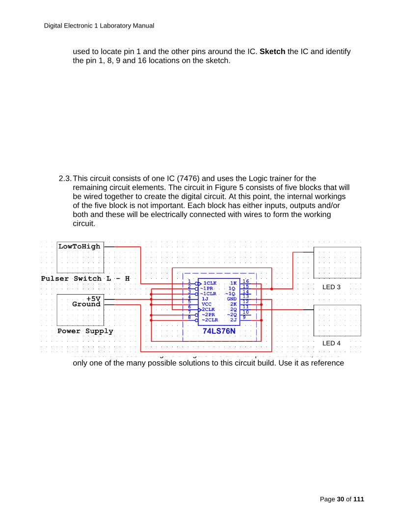
2.3. This circuit consists of one IC (7476) and uses the Logic trainer for the remaining circuit elements. The circuit in Figure 5 consists of five blocks that will be wired together to create the digital circuit. At this point, the internal workings of the five block is not important. Each block has either inputs, outputs and/or both and these will be electrically connected with wires to form the working circuit.
Figure 5
2.4. Place the IC in the breadboard so the IC leads are straddling the gap in the breadboard and are fully inserted into the socket holes. New IC’s may need to be formed to fit into the breadboard without damaging the leads. Ask the instructor for help to form the leads.
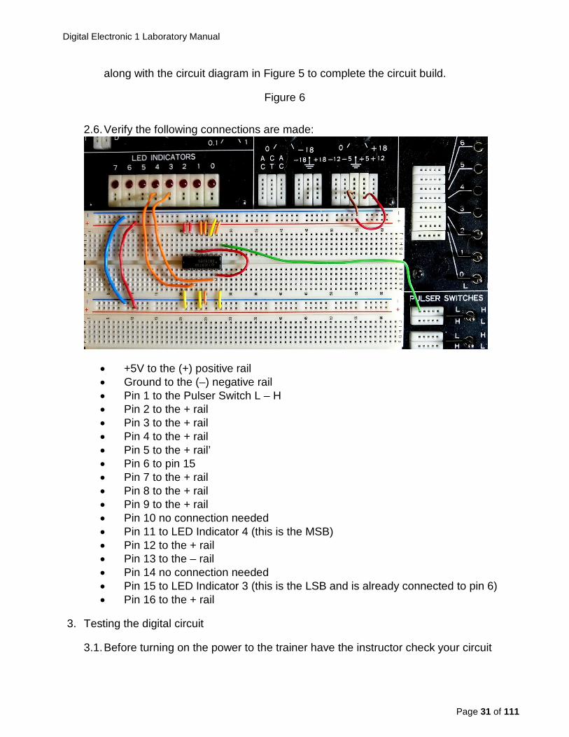
2.5. Use the precut jumpers from your wire kit or cut jumpers to length to electrically connect the five blocks of the circuit. Use the shortest wire possible to complete each connection. Long wires make it more difficult to troubleshoot and can induce noise into the circuit. If possible lay the wires flush against the breadboard as seen in Figure 6. Figure 6 is an example of this circuit, but it is only one of the many possible solutions to this circuit build. Use it as reference
LED 3
LED 4
Page 30 of 111
Digital Electronic 1 Laboratory Manual
along with the circuit diagram in Figure 5 to complete the circuit build.
Figure 6
2.6. Verify the following connections are made:
• +5V to the (+) positive rail • Ground to the (–) negative rail • Pin 1 to the Pulser Switch L – H • Pin 2 to the + rail • Pin 3 to the + rail • Pin 4 to the + rail • Pin 5 to the + rail’ • Pin 6 to pin 15 • Pin 7 to the + rail • Pin 8 to the + rail • Pin 9 to the + rail • Pin 10 no connection needed • Pin 11 to LED Indicator 4 (this is the MSB) • Pin 12 to the + rail • Pin 13 to the – rail • Pin 14 no connection needed • Pin 15 to LED Indicator 3 (this is the LSB and is already connected to pin 6) • Pin 16 to the + rail
3. Testing the digital circuit
3.1. Before turning on the power to the trainer have the instructor check your circuit
Page 31 of 111

Digital Electronic 1 Laboratory Manual
and initial: __________________.
3.2. Turn the trainer power on and record the initial state (0 pulse) of the two LEDs (3 & 4) in Table 1. Do not touch the circuit or any of the controls on the trainer.
Table 1
3.3. Pulse the circuit once by moving the pulser switch lever to the right and releasing (toggling the switch). The lever should return to its original position since it is spring loaded. The LEDs should have changed states.
Pulse Number
LED 4 State (ON or OFF)
LED 3 State (ON or OFF)
Binary Value of LEDs
Decimal Value of
LEDs
Hexadecimal Value of
LEDs
0
1
2
3
4
5
6
7
8
9
Page 32 of 111
Digital Electronic 1 Laboratory Manual
3.4. Record the LED states in Table 1.
3.5. Repeat steps 3.3 and 3.4 for nine pulses. The two LED state columns should be completed. Do not toggle the switch again.
3.6. Using a zero (0) as the OFF state and one (1) as the ON state determine the binary value for each LED 3 and 4 combination in the table.
3.7. Calculate the decimal and hexadecimal values for the last two columns in the table.
3.8. Without toggling the switch, what would the binary value be after the 12th pulse? How did you determine this value?
3.9. Without toggling the switch, what would the hexadecimal value be after the 29th pulse? How did you determine this value?
3.10. Toggle the switch until one LED is ON and one LED is OFF. Leave the trainer power on and use the logic probe and DMM to make the measurements in Table 2.
# DMM Lead Location Logic Probe
(HI / LOW) DMM (V)
Page 33 of 111
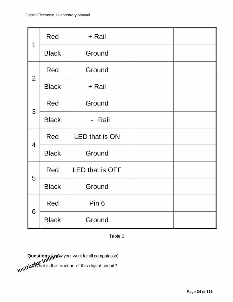
Digital Electronic 1 Laboratory Manual
1 Red + Rail
Black Ground
2 Red Ground
Black + Rail
3 Red Ground
Black - Rail
4 Red LED that is ON
Black Ground
5 Red LED that is OFF
Black Ground
6 Red Pin 6
Black Ground
Table 2
Questions (show your work for all computation):
1. What is the function of this digital circuit?
Page 34 of 111

Digital Electronic 1 Laboratory Manual
2. In table 2, what is the relationship between measurement #1 and measurement #2? Explain your answer.
3. In table 2, explain the value in measurement #3. What does it represent?
4. Complete the table by converting binary, decimal and hexadecimal numbers.
Problem # Binary Decimal Hexadecimal
1 1010 1010
2 253
3 55
Page 35 of 111

Digital Electronic 1 Laboratory Manual
Experiment 4 AND, OR and NOT Gates
Objectives:
• To understand the behavior and demonstrate the operation of AND, OR and NOT gates
• To apply knowledge of the fundamental gates to create truth tables • To develop digital circuit building and troubleshooting skills • To understand key elements of TTL logic specification or datasheets
Text References: Tocci Chapter 3 Sections 3-1 through 3-5
Components Needed:
• One 7408 IC – quad two-input AND gate • One 7432 IC – quad two-input OR gate • One 7404 IC – hex inverter (NOT gate)
Equipment Needed:
• Knight electronics ML-2001 logic trainer • Digital Multimeter • Logic Probe
Discussion:
Gate circuits are the foundation for all digital circuits, and the AND, OR and NOT gates are three of the basic gates. All these gates are packaged in chips that contain multiple gates and are considered Small Scale Integration (SSI) since the packages have less 12 gates per chip. All the chips used in this laboratory manual are dual inline pin (DIP) packages which allows for easy insertion into the breadboard and for easy access to the leads (pins) for troubleshooting. Each chip used in any of the experiments has a manufacturers’ specification (data) sheet available on the internet, but they are also posted on the Blackboard course site under Data Sheets.
These logic gates will respond to HIGH and LOW voltages and since all the chips are TTL based the corresponding voltages will be approximately +5V for HIGH and 0V for LOW. Also, only positive logic is considered in the laboratory manual so a HIGH will correspond with a Boolean logic 1 and a LOW will correspond to a Boolean logic 0. In this lab, each of the gate types will be thoroughly tested and the inputs and outputs mapped into a truth table.
Page 36 of 111

Digital Electronic 1 Laboratory Manual
Troubleshooting Method:
If at any time during the experiment the results do not match the theoretical or expected results use the logic probe to troubleshoot the circuit. There are many approaches to troubleshooting and as you gain experience your method may change, but this is a good basic method to troubleshoot the circuits in this course.
• First, recognize the location of the visual fault. For example, the LED 1 is always on or the display does not show the correct value. The goal is to determine why the visual fault exists. The location of the visual fault is the starting point of the troubleshooting, but the actual root cause of this fault may be located elsewhere in the circuit.
• Next use the logic probe to check for power (HIGH) and ground (LOW) voltages at the first chip in the signal chain that is closest to the visual fault. Once all the power and ground voltages have been verified the focus will be on the individual signals that feed into this chip.
• Since the troubleshooting method is starting at the visual fault area there should be an incorrect output signal. Locate the incorrect output signal(s). Use the logic diagrams, datasheets, schematics and logic probe to trace the incorrect signal back towards the source of the signal. This may involve verifying other inputs to the chip are correct.
• If the incorrect signal leads to another chip first verify the power and ground voltages to the chip and then continue to trace the incorrect signal back to it source.
• The goal is to locate where the incorrect signal has gone correct. At this point the focus would be on understand why the correct signal has gone bad at that location. They are many possible causes of a circuit not functioning properly. It is important to gain experience and build confidence in troubleshooting.
Developing effective troubleshooting skills are like learning to ice skate. We can read about how to ice skate till the cows come home, but at some point you need to get on the ice and try to skate. The actual experience and trial and error is the best way to learn how to ice skate and troubleshoot electrical circuits.
Again, as you gain experience you may want to consider a troubleshooting method that utilizes a “divide and conquer” approach. When done properly this method can shorten the time to locate the fault. Troubleshooting is a skill that enhances value as an employee.
Page 37 of 111
Digital Electronic 1 Laboratory Manual
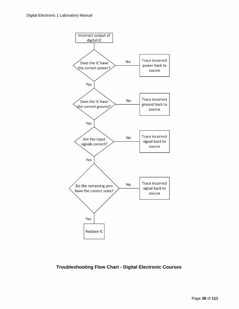
Troubleshooting Flow Chart - Digital Electronic Courses
Page 38 of 111
Digital Electronic 1 Laboratory Manual
Procedure:
1. The AND Gate
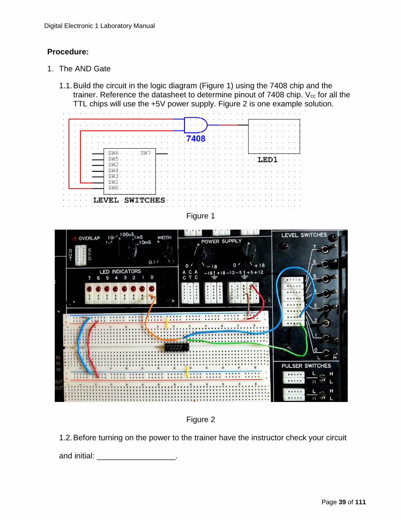
1.1. Build the circuit in the logic diagram (Figure 1) using the 7408 chip and the trainer. Reference the datasheet to determine pinout of 7408 chip. Vcc for all the TTL chips will use the +5V power supply. Figure 2 is one example solution.
Figure 1
Figure 2
1.2. Before turning on the power to the trainer have the instructor check your circuit and initial: __________________.
Page 39 of 111
Digital Electronic 1 Laboratory Manual
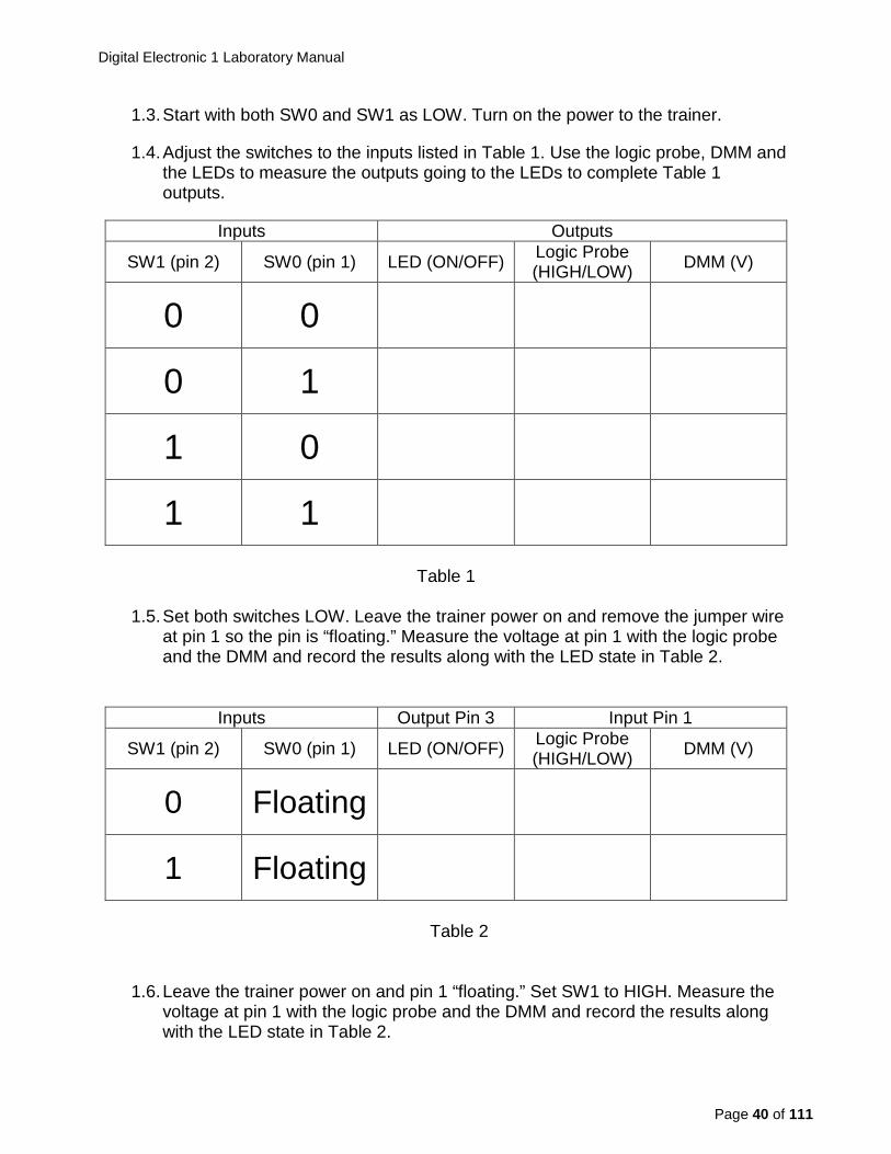
1.3. Start with both SW0 and SW1 as LOW. Turn on the power to the trainer.
1.4. Adjust the switches to the inputs listed in Table 1. Use the logic probe, DMM and the LEDs to measure the outputs going to the LEDs to complete Table 1 outputs.
Inputs Outputs
SW1 (pin 2) SW0 (pin 1) LED (ON/OFF) Logic Probe (HIGH/LOW) DMM (V)
0 0
0 1
1 0
1 1
Table 1
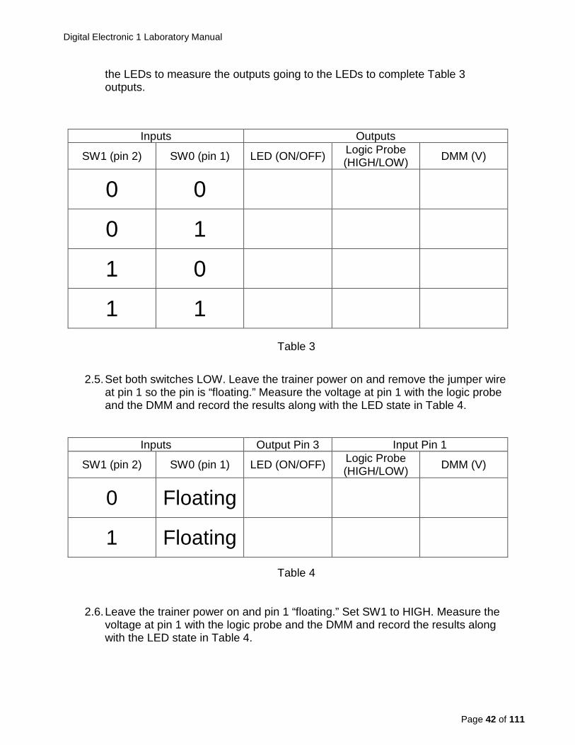
1.5. Set both switches LOW. Leave the trainer power on and remove the jumper wire
at pin 1 so the pin is “floating.” Measure the voltage at pin 1 with the logic probe and the DMM and record the results along with the LED state in Table 2.
Inputs Output Pin 3 Input Pin 1
SW1 (pin 2) SW0 (pin 1) LED (ON/OFF) Logic Probe (HIGH/LOW) DMM (V)
0 Floating
1 Floating
Table 2
1.6. Leave the trainer power on and pin 1 “floating.” Set SW1 to HIGH. Measure the voltage at pin 1 with the logic probe and the DMM and record the results along with the LED state in Table 2.
Page 40 of 111
Digital Electronic 1 Laboratory Manual
1.7. Summarize your results from Table 2.
______________________________________________________________________
______________________________________________________________________
______________________________________________________________________
______________________________________________________________________
______________________________________________________________________
2. The OR Gate
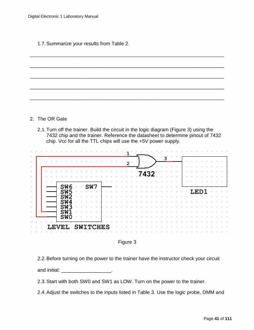
2.1. Turn off the trainer. Build the circuit in the logic diagram (Figure 3) using the 7432 chip and the trainer. Reference the datasheet to determine pinout of 7432 chip. Vcc for all the TTL chips will use the +5V power supply.
Figure 3
2.2. Before turning on the power to the trainer have the instructor check your circuit and initial: __________________. 2.3. Start with both SW0 and SW1 as LOW. Turn on the power to the trainer.
2.4. Adjust the switches to the inputs listed in Table 3. Use the logic probe, DMM and
Page 41 of 111
Digital Electronic 1 Laboratory Manual
the LEDs to measure the outputs going to the LEDs to complete Table 3 outputs.
Inputs Outputs
SW1 (pin 2) SW0 (pin 1) LED (ON/OFF) Logic Probe (HIGH/LOW) DMM (V)
0 0
0 1
1 0
1 1
Table 3
2.5. Set both switches LOW. Leave the trainer power on and remove the jumper wire
at pin 1 so the pin is “floating.” Measure the voltage at pin 1 with the logic probe and the DMM and record the results along with the LED state in Table 4.
Inputs Output Pin 3 Input Pin 1
SW1 (pin 2) SW0 (pin 1) LED (ON/OFF) Logic Probe (HIGH/LOW) DMM (V)
0 Floating
1 Floating
Table 4
2.6. Leave the trainer power on and pin 1 “floating.” Set SW1 to HIGH. Measure the voltage at pin 1 with the logic probe and the DMM and record the results along with the LED state in Table 4.
Page 42 of 111
Digital Electronic 1 Laboratory Manual
2.7. Summarize your results from Table 4.
______________________________________________________________________
______________________________________________________________________
______________________________________________________________________
______________________________________________________________________
______________________________________________________________________
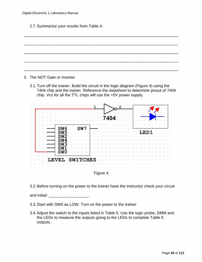
3. The NOT Gate or Inverter
3.1. Turn off the trainer. Build the circuit in the logic diagram (Figure 4) using the 7404 chip and the trainer. Reference the datasheet to determine pinout of 7404 chip. Vcc for all the TTL chips will use the +5V power supply.
Figure 4
3.2. Before turning on the power to the trainer have the instructor check your circuit and initial: __________________. 3.3. Start with SW0 as LOW. Turn on the power to the trainer.
3.4. Adjust the switch to the inputs listed in Table 5. Use the logic probe, DMM and the LEDs to measure the outputs going to the LEDs to complete Table 5 outputs.
Page 43 of 111

Digital Electronic 1 Laboratory Manual
Inputs Outputs
SW0 (pin 1) LED (ON/OFF) Logic Probe (HIGH/LOW) DMM (V)
0
1
Table 5
3.5. Leave the trainer power on and remove the jumper wire at pin 1 so the pin is
“floating.” Measure the voltage at pin 1 with the logic probe and the DMM and record the results along with the LED state in Table 6.
Inputs Output Pin 2 Input Pin 1
SW0 (pin 1) LED (ON/OFF) Logic Probe (HIGH/LOW) DMM (V)
Floating
Table 6
3.6. Summarize your results from Table 6.
______________________________________________________________________
______________________________________________________________________
______________________________________________________________________
______________________________________________________________________
______________________________________________________________________
Questions:
1. How many AND gates are in a 7408 chip? Draw the chip, label and number its pins.
Page 44 of 111

Digital Electronic 1 Laboratory Manual
2. How many OR gates are in a 7432 chip? Draw the chip, label and number its pins.
3. How many NOT gates are in a 7404 chip? Draw the chip, label and number its pins.
4. What voltage do you expect to see at a floating TTL gate output?
5. What logic state do you expect to see at a floating TTL gate output?
6. What voltage is Vcc?
7. Assume that you need a gate that is only HIGH when all the inputs are HIGH. What type of gate do you select?
Page 45 of 111

Digital Electronic 1 Laboratory Manual
8. Draw the logic symbol for a two-input AND gate (label the inputs A and B with an output X). Also create its truth table.
9. Draw the logic symbol for a three-input OR gate (label the inputs A, B and C with an output X). Also create its truth table.
10. Draw the logic symbol for a NOT gate and create its truth table.
11. Draw the logic symbol for an inverter and create its truth table.
Page 46 of 111

Digital Electronic 1 Laboratory Manual
Experiment 5 Basic Combinational Logic & Gates with Many Inputs
Objectives:
• To design basic logic circuits with more than two-inputs • To implement logic circuits from a Boolean expression • To determine the Boolean expression from a logic circuit • To understand how to use AND, OR and NOT gates to create a simply combinational
logic circuit • To develop digital circuit building and troubleshooting skills
Text References: Tocci Chapter 3 Sections 3-6 through 3-8
Components Needed:
• One 7408 IC – quad two-input AND gate • One 7432 IC – quad two-input OR gate • One 7404 IC – hex inverter (NOT gate)
Equipment Needed:
• Knight electronics ML-2001 logic trainer • Logic Probe
Discussion: Up to now, all previous experiments have had logic diagrams with only two logic inputs, but what if a circuit needed three or four inputs? We will look at two ways to address the greater than two-input design. First, there are chips designed for more than three inputs and these chips will be explored in future experiments. Secondly, two-input devices can be combined to create three of more inputs. Think of ways to combine two 7408 chips to create a three input AND gate. This will be the first experiment. Digital logic is implemented by using basic logic gates (AND, OR and NOT) as building blocks to create more complex circuits. A combinational circuit is a group of gates whose output function is only dependent on the values of its current input states (i.e. there is no storage or feedback is present in the circuit). The following circuits are simply combinational circuits.
X = AB’ + A’B or Y = AB + C or Z = (A + B)C
Page 47 of 111

Digital Electronic 1 Laboratory Manual
In the second experiment, these combinational circuits will be built, tested and evaluated. These simply combinational circuits are the basis for more complex logic circuit and chips. Procedures: 1. Gates with More Than Two-inputs
1.1. Design and draw the logic diagram below for a three input AND gate using only one 7408 (quad two-input AND gate chip). The Boolean expression would be
W = ABC
Only include the logic inputs and outputs in the logic diagram. Vcc and ground are always connected but standard practice is to eliminate them from logic diagrams. This helps keep the logic diagram neater and easier to read.
1.2. Build the circuit from the logic diagram above using the 7408 chip and the trainer. Remember that the 7408 IC has four AND gates within the package. Use the Level Switches to toggle the inputs. Reference the datasheet to determine the pinout of the 7408 chip. Vcc for all the TTL chips will use the +5V power supply.
1.3. Before turning on the power to the trainer have the instructor check your circuit
and initial: __________________. 1.4. Start with all the input switches as LOW. Turn on the power to the trainer. If at
any time during the experiment the results do not match the theoretical or expected results use the logic probe to troubleshoot the circuit.
1.5. Adjust the switches to the inputs listed in Table 1. Use the logic probe to measure the output state going to the LED and complete Table 1 outputs.
Page 48 of 111
Digital Electronic 1 Laboratory Manual
Inputs Outputs (W) A B C LED (ON/OFF) Logic Probe
(HIGH/LOW)
0 0 0
0 0 1
0 1 0
0 1 1
1 0 0
1 0 1
1 1 0
1 1 1
Table 1
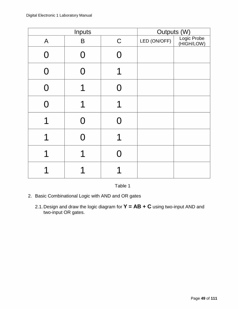
2. Basic Combinational Logic with AND and OR gates
2.1. Design and draw the logic diagram for Y = AB + C using two-input AND and two-input OR gates.
Page 49 of 111
Digital Electronic 1 Laboratory Manual
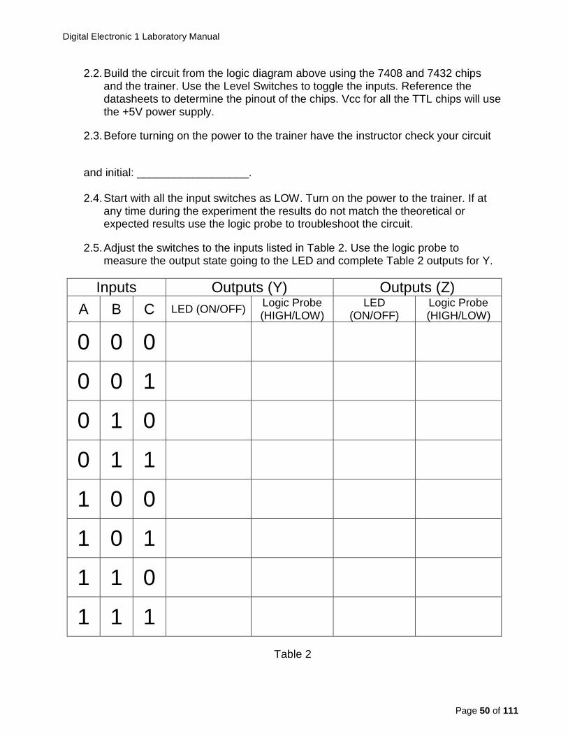
2.2. Build the circuit from the logic diagram above using the 7408 and 7432 chips and the trainer. Use the Level Switches to toggle the inputs. Reference the datasheets to determine the pinout of the chips. Vcc for all the TTL chips will use the +5V power supply.
2.3. Before turning on the power to the trainer have the instructor check your circuit
and initial: __________________. 2.4. Start with all the input switches as LOW. Turn on the power to the trainer. If at
any time during the experiment the results do not match the theoretical or expected results use the logic probe to troubleshoot the circuit.
2.5. Adjust the switches to the inputs listed in Table 2. Use the logic probe to measure the output state going to the LED and complete Table 2 outputs for Y.
Inputs Outputs (Y) Outputs (Z) A B C LED (ON/OFF) Logic Probe
(HIGH/LOW) LED
(ON/OFF) Logic Probe (HIGH/LOW)
0 0 0
0 0 1
0 1 0
0 1 1
1 0 0
1 0 1
1 1 0
1 1 1
Table 2
Page 50 of 111

Digital Electronic 1 Laboratory Manual
2.6. Design and draw the logic diagram for Z = (A + B)C using two-input AND and two-input OR gates. On the logic diagram label the IC pins to help with wiring the circuit.
2.7. Build the circuit from the logic diagram above using the 7408 chip and the trainer. Remember that the 7408 IC has four AND gates within the package. Use the Level Switches to toggle the inputs. Reference the datasheet to determine the pinout of the 7408 chip. Vcc for all the TTL chips will use the +5V power supply.
2.8. Before turning on the power to the trainer have the instructor check your circuit
and initial: __________________. 2.9. Start with all the input switches as LOW. Turn on the power to the trainer. If at
any time during the experiment the results do not match the theoretical or expected results use the logic probe to troubleshoot the circuit.
2.10. Adjust the switches to the inputs listed in Table 2. Use the logic probe to measure the output state going to the LED and complete Table 2 outputs for Z.
2.11. Compare the results in Table 2 for outputs Y and Z and explain the differences. Remember the Order of Operation for Boolean expressions which states AND operations must be performed before OR operations unless there are parentheses are used. The operation within the parentheses must be performed first.
Page 51 of 111

Digital Electronic 1 Laboratory Manual
3. Basic Combinational Logic with AND, OR and NOT gates
3.1. Design and draw the logic diagram for X = AB’ + A’C using two-input ANDs, a two-input OR and inverter gates. On the logic diagram label the IC pins to help with wiring the circuit.
3.2. Build the circuit from the logic diagram above using the 7408, 7432 and 7404 chips and the trainer. Use the Level Switches to toggle the inputs. Reference the datasheets to determine the pinout of the chips. Vcc for all the TTL chips will use the +5V power supply.
3.3. Before turning on the power to the trainer have the instructor check your circuit
and initial: __________________. 3.4. Start with all the input switches as LOW. Turn on the power to the trainer. If at
any time during the experiment the results do not match the theoretical or expected results use the logic probe to troubleshoot the circuit.
3.5. Adjust the switches to the inputs listed in Table 3. Use the logic probe to measure the output state going to the LED and complete Table 3 outputs.
Page 52 of 111
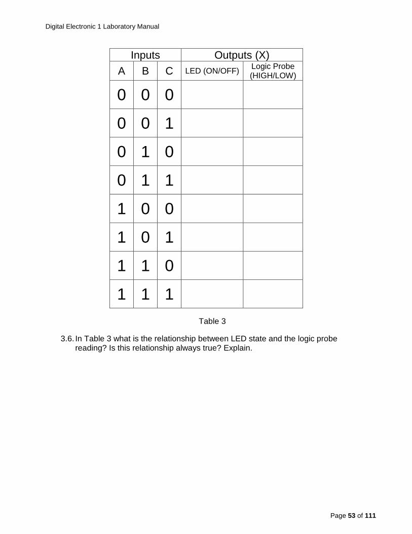
Digital Electronic 1 Laboratory Manual
Inputs Outputs (X) A B C LED (ON/OFF) Logic Probe
(HIGH/LOW)
0 0 0
0 0 1
0 1 0
0 1 1
1 0 0
1 0 1
1 1 0
1 1 1
Table 3
3.6. In Table 3 what is the relationship between LED state and the logic probe reading? Is this relationship always true? Explain.
Page 53 of 111

Digital Electronic 1 Laboratory Manual
Questions:
1. Create the truth table for W = ABC from table 1.
2. Create the truth table for Z = (A + B)C from table 2.
3. Create the truth table for Y = AB + C from table 2.
Page 54 of 111

Digital Electronic 1 Laboratory Manual
4. Create the truth table for X = AB’ + A’B from table 3.
5. Write the Boolean equation for the logic diagram in Figure 1.
Figure 1
6. Draw the logic diagram for a five-input AND gate using only two-input AND gates. Label the inputs and outputs.
Page 55 of 111

Digital Electronic 1 Laboratory Manual
7. Draw the logic diagram for a six-input AND gate using only 5 two-input AND gates. Label the inputs and outputs.
8. Draw the logic diagram for the following Boolean equation: 𝑿𝑿 = (𝑨𝑨𝑨𝑨 + 𝑨𝑨𝑨𝑨����) + 𝑨𝑨𝑨𝑨�𝑨𝑨
Page 56 of 111
Digital Electronic 1 Laboratory Manual
Experiment 6 Basic Boolean Simplification & DeMorgan’s Theorem
Objectives:
• To verify the basic rules of Boolean algebra using logic gates • To verify the two elements of DeMorgan’s Theorem • To develop digital circuit building and troubleshooting skills
Text References: Tocci Chapter 3 Sections 3-10 through 3-13
Components Needed:
• One 7408 IC – quad two-input AND gate • One 7432 IC – quad two-input OR gate • One 7404 IC – hex inverter (NOT gate)
Equipment Needed:
• Knight electronics ML-2001 logic trainer • Logic Probe
Discussion:
Boolean algebra is similar to other mathematical topics in that there are identities that can be used to simplify the work that needs to be done. The basic identities of Boolean algebra are: A + 0 = A A + 1 = 1 A + A = A A + A’ = 1
A*0 = 0 A*1 = A AA = A AA’ = 0
A’’ = A A + AB = A A + A’B = A + B
Page 57 of 111
Digital Electronic 1 Laboratory Manual
Since seeing is believing, this experiment will demonstrate all of the single variable Boolean identities using AND, OR and NOT gates in this experiment.
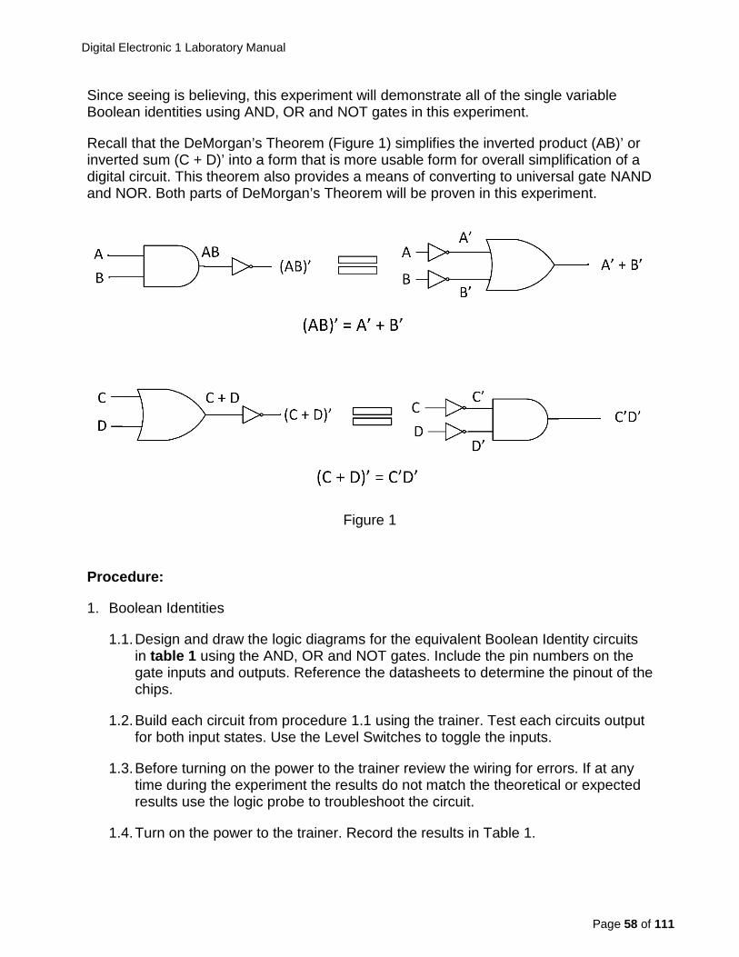
Recall that the DeMorgan’s Theorem (Figure 1) simplifies the inverted product (AB)’ or inverted sum (C + D)’ into a form that is more usable form for overall simplification of a digital circuit. This theorem also provides a means of converting to universal gate NAND and NOR. Both parts of DeMorgan’s Theorem will be proven in this experiment.
Figure 1
Procedure:
1. Boolean Identities
1.1. Design and draw the logic diagrams for the equivalent Boolean Identity circuits in table 1 using the AND, OR and NOT gates. Include the pin numbers on the gate inputs and outputs. Reference the datasheets to determine the pinout of the chips.
1.2. Build each circuit from procedure 1.1 using the trainer. Test each circuits output for both input states. Use the Level Switches to toggle the inputs.
1.3. Before turning on the power to the trainer review the wiring for errors. If at any time during the experiment the results do not match the theoretical or expected results use the logic probe to troubleshoot the circuit.
1.4. Turn on the power to the trainer. Record the results in Table 1.
Page 58 of 111

Digital Electronic 1 Laboratory Manual
Draw the equivalent Boolean identity circuit Boolean Identity
Experimental Result (A, 1, 0)
A + 0 = A
A + 1 = 1
A + A = A
A + A’ = 1
A*0 = 0
A*1 = A
AA = A
AA’ = 0
A’’ = A
Table 1
1.5. Describe your results and comment on any problems encountered during the build and testing the circuits for Table 1?
Page 59 of 111

Digital Electronic 1 Laboratory Manual
2. DeMorgan’s Theorem
2.1. Design and draw the first element of DeMorgan’s Theorem (AB)’ = A’ + B’ using the AND, OR and NOT gates. Include the pin numbers on the gate inputs and outputs. Reference the datasheets to determine the pinout of the chips.
(AB)’
A’ + B’
2.2. Use the AND, OR and NOT gates along with the trainer to build the two logic circuits from the first DeMorgan’s Theorem (AB)’ = A’ + B’.Use the Level Switches to toggle the inputs.
2.3. Before turning on the power to the trainer review the wiring for errors.
2.4. Start with all the input switches as LOW. Turn on the power to the trainer. If at any time during the experiment the results do not match the theoretical or expected results use the logic probe to troubleshoot the circuit.
2.5. Adjust the switches to test all the input combinations and record the results in Table 2.
Page 60 of 111

Digital Electronic 1 Laboratory Manual
Inputs Outputs A B (AB)’ A’ + B’
Table 2
2.6. Comment on the results of Table 2.
2.7. Design and draw the second element of DeMorgan’s Theorem (C + D)’ = C’D’ using the AND, OR and NOT gates. Include the pin numbers on the gate inputs and outputs. Reference the datasheets to determine the pinout of the chips.
(C + D)’
C’D’
Page 61 of 111

Digital Electronic 1 Laboratory Manual
2.8. Use the AND, OR and NOT gates along with the trainer to build the two logic circuits from the second DeMorgan’s Theorem (C + D)’ = C’D’. Use the Level Switches to toggle the inputs.
2.9. Before turning on the power to the trainer review the wiring for errors.
2.10. Start with all the input switches as LOW. Turn on the power to the trainer. If at any time during the experiment the results do not match the theoretical or expected results use the logic probe to troubleshoot the circuit.
2.11. Adjust the switches to test all the input combinations and record the results in Table 3.
Inputs Outputs C D (C + D)’ C’D’
Table 3
2.12. Comment on the results of Table 3.
Page 62 of 111

Digital Electronic 1 Laboratory Manual
Questions:
1. Simplify the Boolean equation M = W’XY’ + WXY’ + XY’Z using Boolean identities and theorems to show that M = XY’
2. Draw the logic diagrams for X = AB(A’ + BC)’ and Y = ABC’.
3. Using Boolean identities and the DeMorgan’s Theorem prove that X = Y from question 2.
Page 63 of 111

Digital Electronic 1 Laboratory Manual
Experiment 7 NAND Gates and the Universality of NAND Gates
Objectives:
• To understand the behavior and demonstrate the operation of the NAND gate • To demonstrate the universality of the NAND gate • To build a combinational logic circuit using all NAND gates • To develop digital circuit building and troubleshooting skills
Text References: Tocci Chapter 3 Sections 3-9 through 3-12
Components Needed:
• One 7404 IC – hex inverter (NOT gate) • One 7408 IC – quad two-input AND gate • Two 7420 IC – four-input NAND gate • One 7432 IC – quad two-input OR gate
Equipment Needed:
• Knight electronics ML-2001 logic trainer • Logic Probe
Discussion:
The basic logic gates AND, OR and NOT can be combined to make any other logic gate. The NAND gate is a derived gate and is special since it is considered a universal gate. It is a NOT AND gate and the logic symbol is the AND gate with an invert bubble on its output as in Figure 1. Like the AND and OR gates the NAND gate can more than two inputs.
The universality of the NAND gate means any Boolean expression may be implemented with all NAND gates without the use of any other logic type gate. This will be demonstrated in the second experiment. NAND is a preferred universal gate since it is easier and more economical to manufacture than other universal gates, such as NOR gates.
Figure 1
Page 64 of 111

Digital Electronic 1 Laboratory Manual
Procedures:
1. NAND Gates
1.1. Design and draw the logic diagram for a two-input NAND gate using one two-input AND and one NOT gate. Include the pin numbers on the gate inputs and outputs.
1.2. Build the NAND gate circuit above using the 7408 and 7404 chips and the
trainer. Use the Level Switches to toggle the inputs. Reference the datasheets to determine the pinout of the chips. Vcc for all the TTL chips will use the +5V power supply.
1.3. Before turning on the power to the trainer review the wiring for errors. If at any
time during the experiment the results do not match the theoretical or expected results use the logic probe to troubleshoot the circuit.
Table 1
Inputs Outputs A B AND AND - NOT NAND
0 0
0 1
1 0
1 1
Page 65 of 111
Digital Electronic 1 Laboratory Manual
Figure 2 – NAND Gate Equivalent Circuits
1.4. Start with all the input switches as LOW. Turn on the power to the trainer. If at any time during the experiment the results do not match the theoretical or expected results use the logic probe to troubleshoot the circuit.
1.5. Adjust the switches to the inputs listed in Table 1. Record the output states (AND and AND-NOT) for each input combination.
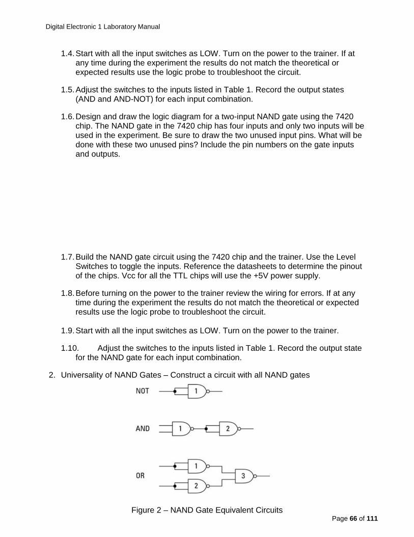
1.6. Design and draw the logic diagram for a two-input NAND gate using the 7420 chip. The NAND gate in the 7420 chip has four inputs and only two inputs will be used in the experiment. Be sure to draw the two unused input pins. What will be done with these two unused pins? Include the pin numbers on the gate inputs and outputs.
1.7. Build the NAND gate circuit using the 7420 chip and the trainer. Use the Level
Switches to toggle the inputs. Reference the datasheets to determine the pinout of the chips. Vcc for all the TTL chips will use the +5V power supply.
1.8. Before turning on the power to the trainer review the wiring for errors. If at any time during the experiment the results do not match the theoretical or expected results use the logic probe to troubleshoot the circuit.
1.9. Start with all the input switches as LOW. Turn on the power to the trainer.
1.10. Adjust the switches to the inputs listed in Table 1. Record the output state for the NAND gate for each input combination.
2. Universality of NAND Gates – Construct a circuit with all NAND gates
Page 66 of 111
Digital Electronic 1 Laboratory Manual
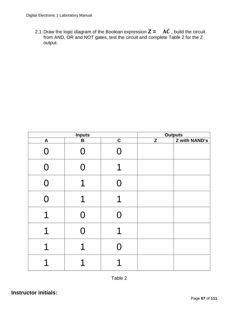
2.1. Draw the logic diagram of the Boolean expression Z = + 𝐀𝐀𝐂𝐂� , build the circuit from AND, OR and NOT gates, test the circuit and complete Table 2 for the Z output.
Table 2
Inputs Outputs A B C Z Z with NAND’s
0 0 0
0 0 1
0 1 0
0 1 1
1 0 0
1 0 1
1 1 0
1 1 1
Instructor initials: Page 67 of 111

Digital Electronic 1 Laboratory Manual
2.2. Using the NAND gate equivalent circuits from Figure 2 and redraw the logic diagram (from 2.1) using only NAND gates.
Questions:
1. What is the truth table and logic symbol for a two-input NAND gate (inputs A and B with output X)?
2. Compare both outputs of Z in Table 2 and comment.
Page 68 of 111
Digital Electronic 1 Laboratory Manual
3. If the 7400 (quad two-input NAND gate) chip was used instead of the 7420 (four-input NAND gate) chip how many 7400 chips would be needed for the design? Is that more or less than in the AND-OR-NOT design? Show the 7400 design.
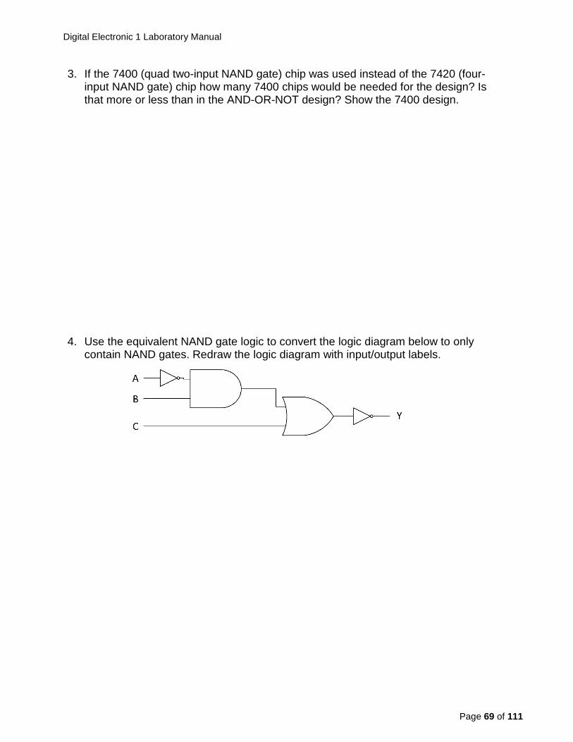
4. Use the equivalent NAND gate logic to convert the logic diagram below to only contain NAND gates. Redraw the logic diagram with input/output labels.
Page 69 of 111
Digital Electronic 1 Laboratory Manual
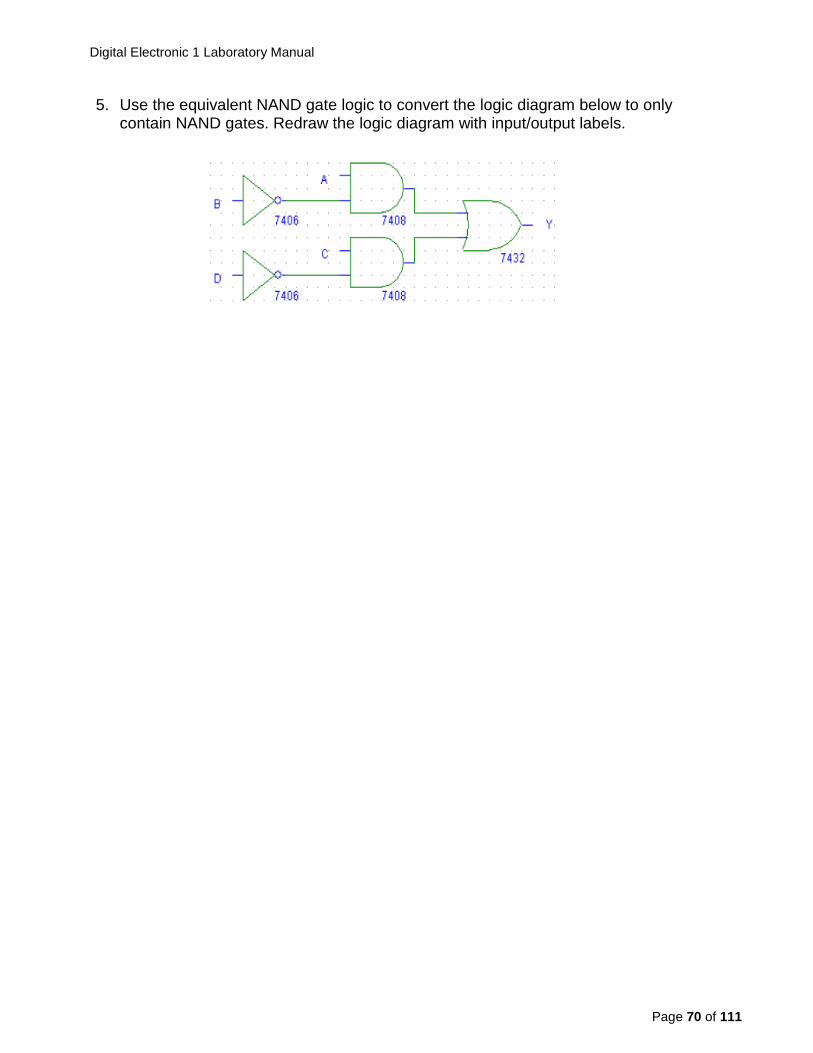
5. Use the equivalent NAND gate logic to convert the logic diagram below to only contain NAND gates. Redraw the logic diagram with input/output labels.
Page 70 of 111

Digital Electronic 1 Laboratory Manual
Experiment 8/9 (Two Weeks) BCD Detector Project With Karnaugh Maps
Objectives:
• To understand the Sum-of-Product (SOP) form • To apply the Karnaugh map method to simplify a Boolean equation • To apply “don’t care” states to a Karnaugh Map (K-map) • To create a MultiSim simulation of a digital circuit • To develop digital circuit building and troubleshooting skills
Text References: Tocci Chapter 4 Sections 4-1 through 4-5
Components Needed: (quantities unknown)
• 7400 IC – quad two-input NAND gate • 7404 IC – hex inverter (NOT gate) • 7408 IC – quad two input AND gate • 7420 IC – 4-input NAND gate • 7432 IC – quad two input OR gate
Equipment Needed:
• Knight electronics ML-2001 logic trainer • Logic Probe
Discussion:
As has been demonstrated in lecture, the Karnaugh map (K-map) method of simplification is a powerful graphical technique that uses the Sum-of-Products (SOP) form. The advantages of using K-maps for reduction is that it is easier to see when the expression has been fully simplified and the K-map method provides a structured approach to Boolean simplification.
In the experiment, a BCD detector will be designed, implemented in MultiSim, simplified using a K-map, designs built and tested. A truth table will need to be created before a K-map can be employed, so start thinking about how to create a truth table for a BCD detector and the specifications that follow. Cost of this BCD detector is also a factor, so designs need to consider the cost as changes are made. The specification for the BCD detector is as follows:
Page 71 of 111
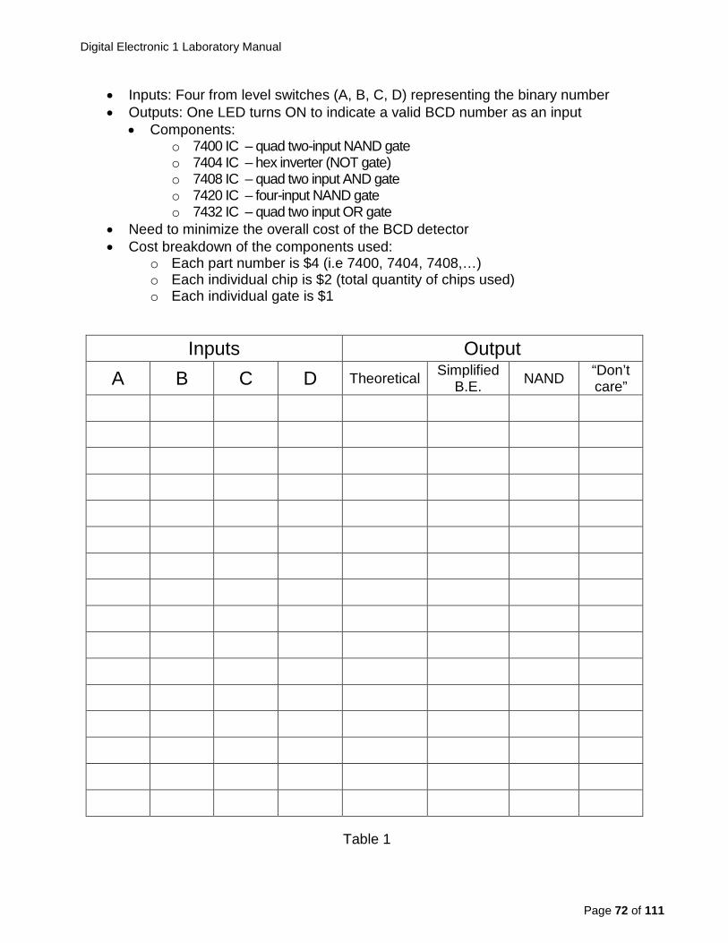
Digital Electronic 1 Laboratory Manual
• Inputs: Four from level switches (A, B, C, D) representing the binary number • Outputs: One LED turns ON to indicate a valid BCD number as an input
• Components: o 7400 IC – quad two-input NAND gate o 7404 IC – hex inverter (NOT gate) o 7408 IC – quad two input AND gate o 7420 IC – four-input NAND gate o 7432 IC – quad two input OR gate
• Need to minimize the overall cost of the BCD detector • Cost breakdown of the components used:
o Each part number is $4 (i.e 7400, 7404, 7408,…) o Each individual chip is $2 (total quantity of chips used) o Each individual gate is $1
Table 1
Inputs Output A B C D Theoretical Simplified
B.E. NAND “Don’t care”
Page 72 of 111

Digital Electronic 1 Laboratory Manual
Procedure:
1. Create simulation of BCD detector
1.1. Create a truth table (above) from the information in the specifications.
1.2. Derive the Boolean equation in the Sum-of –Product form from the truth table (Table 1).
1.3. Implement the not simplified Boolean equation (SOP) on MultiSim using the chips called out in the specification.
1.4. Simulate the not simplified Boolean equation on MultiSim. Print out MultiSim circuit with simulation results. This will part of your report.
1.5. Count the number of part numbers used in the simulation and calculate the cost:
Part Cost = total part numbers used * $4
Part Cost = ____________ * $4
1.6. Count the number of individual chips used in the simulation and calculate the cost:
Chip Cost = total number of chips used * $2
Chip Cost = ____________ * $2
1.7. Count the number of individual gates used in the simulation and calculate the cost:
Gate Cost = total number of gates used * $1
Gate Cost = ____________ * $1
1.8. Determine the total cost = part cost + chip cost + gate cost
Total Cost = ___________ + ___________ + ___________
Total Cost = ___________ (original design)
Page 73 of 111

Digital Electronic 1 Laboratory Manual
1.9. Summarize the cost results in the “Original Design” row of Table 2.
Design Part Cost Chip Cost Gate Cost Total Cost Original Design
Simplified Design
NAND Design
“Don’t care” Design
Table 2
2. First prototype
2.1. Use SOP Boolean equation from the truth table to complete a K-map in Figure 1.
Figure 1
2.2. Derive simplified Boolean Equation from the K-map in Figure 1.
Page 74 of 111

Digital Electronic 1 Laboratory Manual
2.3. Draw the logic diagram from the simplified Boolean Equation using the AND, OR and NOT gates. Include the pin numbers on the gate inputs and outputs.
2.4. Use the AND, OR and NOT gates along with the trainer to build the logic circuit. Use the Level Switches to toggle the inputs.
2.5. Before turning on the power to the trainer review the wiring for errors.
2.6. Start with all the input switches as LOW. Turn on the power to the trainer. If at any time during the experiment the results do not match the theoretical or expected results use the logic probe to troubleshoot the circuit.
2.7. Adjust the switches to test all the input combinations and record the results in Table 1 under the “Simplified B.E.” column. Turn off the trainer.
2.8. Count the number of part numbers used in the simplified design and calculate the cost:
Part Cost = total part numbers used * $4
Part Cost = ____________ * $4
2.9. Count the number of individual chips used in the simplified design and calculate the cost:
Chip Cost = total number of chips used * $2
Chip Cost = ____________ * $2
Page 75 of 111

Digital Electronic 1 Laboratory Manual
2.10. Count the number of individual gates used in the simplified design and calculate the cost:
Gate Cost = total number of gates used * $1
Gate Cost = ____________ * $1
2.11. Determine the total cost = part cost + chip cost + gate cost
Total Cost = ___________ + ___________ + ___________
Total Cost = ___________ (simplified design)
2.12. Summarize the cost results in the “Simplified Design” row of Table 2.
3. Second prototype with cost reductions
3.1. Convert the simplified Boolean Equation in SOP form to use only NAND gates. Draw the logic diagram using only NAND gates. Include the pin numbers on the gate inputs and outputs.
3.2. Use the NAND gates along with the trainer to build the logic circuit. Use the Level Switches to toggle the inputs.
3.3. Before turning on the power to the trainer review the wiring for errors.
3.4. Start with all the input switches as LOW. Turn on the power to the trainer. If at any time during the experiment the results do not match the theoretical or expected results use the logic probe to troubleshoot the circuit.
Page 76 of 111

Digital Electronic 1 Laboratory Manual
3.5. Adjust the switches to test all the input combinations and record the results in Table 1 under the “NAND” column. Turn off the trainer.
3.6. Count the number of part numbers used in the NAND gate design and calculate the cost:
Part Cost = total part numbers used * $4
Part Cost = ____________ * $4
3.7. Count the number of individual chips used in the NAND gate design and calculate the cost:
Chip Cost = total number of chips used * $2
Chip Cost = ____________ * $2
3.8. Count the number of individual gates used in the NAND gate design and calculate the cost:
Gate Cost = total number of gates used * $1
Gate Cost = ____________ * $1
3.9. Determine the total cost = part cost + chip cost + gate cost
Total Cost = ___________ + ___________ + ___________
Total Cost = ___________ (NAND gate design)
3.10. Summarize the cost results in the “NAND Gate Design” row of Table 2.
4. Prototype with changes (don’t care state). The change to the specification is the decimal 10 and 11 are no longer options as inputs. This means they are considered “don’t cares” in the K-map, so the K-map and simplification needs to be repeated and a new NAND solution needs to be determined.
4.1. Use the Boolean equation with only NAND functions to complete a K-map in Figure 2. Add in the “don’t care” states for decimal 10 and 11.
Page 77 of 111

Digital Electronic 1 Laboratory Manual
Figure 2
4.2. Derive the Boolean Equation from the K-map with the “don’t care” states in
Figure 2.
4.3. Draw the logic diagram from the “don’t care” Boolean Equation using the AND, OR and NOT gates. Include the pin numbers on the gate inputs and outputs.
4.4. Do not build this design. Convert the “don’t care” logic diagram use to use only NAND gates. Draw the logic diagram using only NAND gates. Include the pin numbers on the gate inputs and outputs.
Page 78 of 111

Digital Electronic 1 Laboratory Manual
4.5. Use the NAND gates along with the trainer to build the logic circuit. Use the Level Switches to toggle the inputs.
4.6. Before turning on the power to the trainer review the wiring for errors.
4.7. Start with all the input switches as LOW. Turn on the power to the trainer. If at any time during the experiment the results do not match the theoretical or expected results use the logic probe to troubleshoot the circuit.
4.8. Adjust the switches to test all the input combinations and record the results in Table 1 under the “Don’t care” column.
4.9. Count the number of part numbers used in the “don’t care” design and calculate the cost:
Part Cost = total part numbers used * $4
Part Cost = ____________ * $4
4.10. Count the number of individual chips used in the “don’t care” design and calculate the cost:
Chip Cost = total number of chips used * $2
Chip Cost = ____________ * $2
4.11. Count the number of individual gates used in the “don’t care” design and calculate the cost:
Gate Cost = total number of gates used * $1
Gate Cost = ____________ * $1
4.12. Determine the total cost = part cost + chip cost + gate cost
Total Cost = ___________ + ___________ + ___________
4.13. Total Cost = ___________ (“don’t care” design)
4.14. Summarize the cost results in the “Don’t Care Design” row of Table 2.
Questions:
1. Why isn’t input D needed in the BCD detector design?
Page 79 of 111

Digital Electronic 1 Laboratory Manual
2. Review the cost table 2 and summarize the results.
3. How many four-input AND gates, three-input OR gates and NOT gates are needed to realize Z?
Z = C’D’(B’ + A’B) + CD’(B’ + A’B)
Z = A’B’C’ D’ + AB’CD’ + AB’C’D’ + A’B’CD’ + A’BC’D’ + A’BCD’ …
4. Use the K-map reduction method to find the simplified Boolean equation for Z.
5. Draw the logic diagram for the simplified Z.
Page 80 of 111

Digital Electronic 1 Laboratory Manual
Experiment 10 S-R & D Latches & J-K Flip Flops
Objectives:
• To understand the S-R latch • To understand the D latch • To understand the operation of an edge triggered J-K flip-flop • To understand the latching abilities of flip-flops
Text References: Tocci Chapter 5 Sections 5-6 through 5-9
Components Needed:
• One 7400 IC – quad two-input NAND gate • One 7404 IC – hex inverter (NOT gate) • One 7476 IC – dual J-K flip-flop
Equipment Needed:
• Knight electronics ML-2001 logic trainer • Logic Probe
Discussion:
Everything to this point has been a combinational logic circuit, meaning there is no feedback or memory. The output is dependent strictly on the input without any type of synchronization. Sequential logic can have a timing mechanism (clock signal) and a form of memory where previous states may influence the next state.
In digital circuits, a fIip-fIop is a device referring to an electronic circuit that has two stable states and is capable of serving as one bit of memory. Flip-flops are a sequential logic device and are usually controlled by control signal(s) and/or a clock signal. The output often includes the complement (Q’) as well as the normal output (Q) and are synchronous devices. Flip-flop are a major element in digital circuits and can be found in data storage, data transfer, counters and frequency division.
Latches are similar to flip-flops but do not use a clock so latches are typically asynchronous devices, meaning when the inputs change the outputs will change as long as the chip is enabled.
In this experiment, two latches and one type of flip-flop will be explored, the S-R latch, the D latch and the J-K flip-flop. We’ll start with the S-R flip-flop since this is the simplest
Page 81 of 111
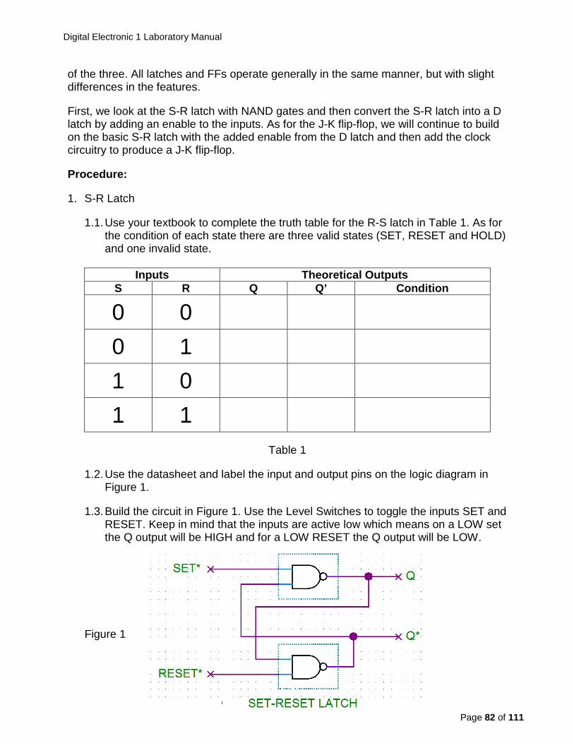
Digital Electronic 1 Laboratory Manual
of the three. All latches and FFs operate generally in the same manner, but with slight differences in the features.
First, we look at the S-R latch with NAND gates and then convert the S-R latch into a D latch by adding an enable to the inputs. As for the J-K flip-flop, we will continue to build on the basic S-R latch with the added enable from the D latch and then add the clock circuitry to produce a J-K flip-flop.
Procedure:
1. S-R Latch
1.1. Use your textbook to complete the truth table for the R-S latch in Table 1. As for the condition of each state there are three valid states (SET, RESET and HOLD) and one invalid state.
Inputs Theoretical Outputs
S R Q Q’ Condition
0 0
0 1
1 0
1 1
Table 1
1.2. Use the datasheet and label the input and output pins on the logic diagram in Figure 1.
1.3. Build the circuit in Figure 1. Use the Level Switches to toggle the inputs SET and RESET. Keep in mind that the inputs are active low which means on a LOW set the Q output will be HIGH and for a LOW RESET the Q output will be LOW.
Figure 1
Page 82 of 111
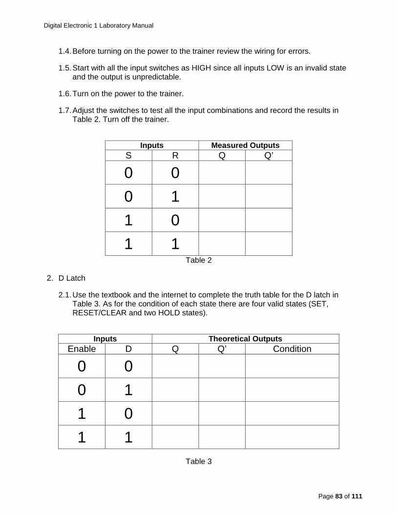
Digital Electronic 1 Laboratory Manual
1.4. Before turning on the power to the trainer review the wiring for errors.
1.5. Start with all the input switches as HIGH since all inputs LOW is an invalid state and the output is unpredictable.
1.6. Turn on the power to the trainer.
1.7. Adjust the switches to test all the input combinations and record the results in Table 2. Turn off the trainer.
Inputs Measured Outputs
S R Q Q’
0 0
0 1
1 0
1 1
Table 2 2. D Latch
2.1. Use the textbook and the internet to complete the truth table for the D latch in Table 3. As for the condition of each state there are four valid states (SET, RESET/CLEAR and two HOLD states).
Inputs Theoretical Outputs
Enable D Q Q’ Condition
0 0
0 1
1 0
1 1
Table 3
Page 83 of 111
Digital Electronic 1 Laboratory Manual
2.2. Use the datasheet and label the input and output pins on the logic diagram in Figure 2.
2.3. Build the circuit in Figure 2. Use the Level Switches to toggle the inputs ENABLE and D.
Figure 2
2.4. Before turning on the power to the trainer review the wiring for errors.
2.5. Start with all the input switches as LOW.
2.6. Turn on the power to the trainer.
2.7. Adjust the switches to test all the input combinations and record the results in Table 4. Turn off the trainer.
Inputs Measured Outputs Previous State Next State
Enable D Q Q’ Q Q’
0 0 X X
0 1
1 0
1 1
Table 4
Page 84 of 111
Digital Electronic 1 Laboratory Manual
3. J-K Flip-Flop
3.1. Use the textbook to complete the truth table for the J-K flip-flop in Table 5. As for the condition of each state be sure to include asynchronous or synchronous along with the state (SET, RESET/CLEAR, TOGGLE, HOLD and INVALID). To keep it simple think of SET = PRESET = 1 for Q and CLEAR = RESET = 0 for Q.
Inputs Theoretical Outputs Experimental Output
J K CLK PRE* CLR* Q & Condition Q & Condition
X X ↓ 0 0
X X ↓ 0 1
X X ↓ 1 0
X X ↓ 1 1
0 0 ↓ 1 1
0 1 ↓ 1 1
1 0 ↓ 1 1
1 1 ↓ 1 1
Table 5
Page 85 of 111
Digital Electronic 1 Laboratory Manual
3.2. Use the datasheet and label the input and output pins on the logic diagram in Figure 3.
Figure 3
3.3. Build the circuit in Figure 3. Use the Level Switches to toggle the inputs and the Pulser Switch to clock the FF.
3.4. Before turning on the power to the trainer review the wiring for errors.
3.5. Turn on the power to the trainer.
3.6. Adjust the switches to test all the input combinations and record the results in Table 5 under the “Experimental Output” column.
3.7. Turn off the trainer. Place the J-K flip-flop in the toggle mode.
3.8. Remove the clock wire from the Pulser Switch and plug it into the CLOCK OUT terminal on the left side of the trainer (see photo).
Page 86 of 111
Digital Electronic 1 Laboratory Manual
3.9. Set the CLOCK frequency to 10 Hz and the Fine Frequency adjustment knob to 0.1.
3.10. Turn the trainer on and describe the LEDs action.
3.11. Turn the Fine Frequency adjustment knob slowly CW and then CCW. Describe what happens to the LEDs.
3.12. When in the toggle mode, if the clock has a 10% duty cycle what would the Q output duty cycle be? Support your answer with a drawing.
Questions:
1. Summarize the relationship between the inputs and output Q in the S-R latch.
Page 87 of 111

Digital Electronic 1 Laboratory Manual
2. Summarize the relationship between the inputs and the output Q in the D latch.
3. What is the difference between the S-R latch and the D latch?
4. List the synchronous inputs for the J-K flip-flop.
5. List the asynchronous inputs for the J-K flip-flop.
Page 88 of 111

Digital Electronic 1 Laboratory Manual
6. What is the difference between a synchronous and an asynchronous input?
7. Describe what the inputs need to be to place the J-K flip-flop in toggle mode.
8. Describe the Q output when the J-K flip-flop is in the toggle mode.
9. Describe the Q’ output when the J-K flip-flop is in the toggle mode.
10. If both PRE* and CLR* are HIGH and J and K are both LOW what effect does the clock have on the output Q?
Page 89 of 111

Digital Electronic 1 Laboratory Manual
Experiment 11 Shift Registers
Objectives:
• To understand the operation of a 4-bit serial load shift register • To develop digital circuit building and troubleshooting skills
Text References: Tocci Chapter 5 Sections 5-14 through 5-17 Components Needed:
• Two 7474 IC – dual D flip-flop
Equipment Needed:
• Knight electronics ML-2001 logic trainer • Logic Probe
Discussion:
Shift registers are another form of sequential logic and are used for storage of binary data or the movement of data. The width of the data that needs to be stored determines how many flip-flops are needed, so the register is a chain of flip-flops where the output of one flip-flop feeds into the input of the next flip-flop. An 8-bit register would have 8 flip-flops in the chain. There are five basic types of shift registers:
• Serial In - Serial Out • Serial In - Parallel Out • Parallel In - Serial Out • Parallel In - Parallel Out • Bidirectional shift registers
This experiment will focus on a 4-bit serial in register which could be used as serial out or parallel out shift register. For the serial in shift registers the data moves one bit at a time on every clock pulse and for serial out it would be the same process. The parallel out feature in a shift register would have all the bits in the register available for movement at the same time or in parallel.
Page 90 of 111
Digital Electronic 1 Laboratory Manual
Procedure:
1. Serial in-Serial out
1.1. Use the datasheet and label the input and output pins on the logic diagram in Figure 1.
Figure 1
1.2. Build the circuit in Figure 1. Use the Level Switches to toggle the inputs (Data and Clear) and the Pulser Switch to clock the FF. Notice the Clear is active LOW and will reset all Q outputs to LOW. All Presets are tied HIGH.
1.3. Before turning on the power to the trainer review the wiring for errors.
1.4. Turn on the power to the trainer.
1.5. Clear the data from the shift register and operate the shift register according to table 1. Do one row at a time and start from the left and work to the right. Record the LED state under outputs in the table for each clock pulse.
1.6. Describe how the data moves.
Page 91 of 111
Digital Electronic 1 Laboratory Manual
Inputs CLK
Pulse Outputs
Step # CLR Data A B C D
1 0 1 0 0 0 0 0 2 1 1 1 3 1 0 2 4 1 0 3 5 1 1 4 6 1 1 5 7 1 1 6 8 1 0 7 9 1 0 8 10 1 0 9 11 1 0 10 12 1 1 11 13 1 1 12 14 1 0 13 15 1 1 14 16 0 1 15 17 1 1 16 18 1 1 17 19 1 1 18 20 0 1 19 21 1 0 20 22 1 1 21 23 1 0 22 24 1 1 23
Table 1
Page 92 of 111

Digital Electronic 1 Laboratory Manual
Questions:
1. What is the major advantage of parallel out over serial out?
2. How many clock pulses are needed to shift one bit through the 4-bit shift register? Support your answer with a drawing of the bit movement.
3. Describe how the shift register built in lab could be use as either serial or parallel out. Support your answer with drawings for both serial and parallel out.
4. What would the register (ABCD) look like at step # 20 if CLR was HIGH?
5. Which bit is the Least Significant Bit (LSB)?
Page 93 of 111
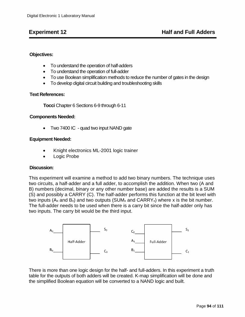
Digital Electronic 1 Laboratory Manual
Experiment 12 Half and Full Adders
Objectives:
• To understand the operation of half-adders • To understand the operation of full-adder • To use Boolean simplification methods to reduce the number of gates in the design • To develop digital circuit building and troubleshooting skills
Text References: Tocci Chapter 6 Sections 6-9 through 6-11
Components Needed:
• Two 7400 IC - quad two input NAND gate
Equipment Needed:
• Knight electronics ML-2001 logic trainer • Logic Probe
Discussion:
This experiment will examine a method to add two binary numbers. The technique uses two circuits, a half-adder and a full adder, to accomplish the addition. When two (A and B) numbers (decimal, binary or any other number base) are added the results is a SUM (S) and possibly a CARRY (C). The half-adder performs this function at the bit level with two inputs (Ax and Bx) and two outputs (SUMx and CARRYx) where x is the bit number. The full-adder needs to be used when there is a carry bit since the half-adder only has two inputs. The carry bit would be the third input.
There is more than one logic design for the half- and full-adders. In this experiment a truth table for the outputs of both adders will be created. K-map simplification will be done and the simplified Boolean equation will be converted to a NAND logic and built.
Page 94 of 111

Digital Electronic 1 Laboratory Manual
Procedure:
1. Half-Adder
1.1. Create the truth table for the SUM (S) and the CARRY (Cout) bit. The inputs are A and B.
Inputs Theoretical Outputs Experimental Outputs
A B S Cout S Cout
Table 1
1.2. Read the Boolean equations from the truth table. It should be in SOP form.
1.3. Draw the logic diagrams for the simplified Boolean equations S and Cout.
Page 95 of 111

Digital Electronic 1 Laboratory Manual
1.4. Convert the logic diagrams for S and Cout to a NAND logic.
1.5. Build the circuits and test. Record the results on Table 1.
1.6. Compare and comment on the Table 1 results.
2. Full-Adder
2.1. Create the truth table for the SUM (S) and the CARRY (Cout) bit. The inputs
are A, B and Cin. Inputs Theoretical Outputs Simulated Outputs
A B Cin S Cout S Cout
Table 2
Page 96 of 111

Digital Electronic 1 Laboratory Manual
2.2. Create two K-maps for outputs S and Cout and derive the simplified Boolean equations (if possible).
2.3. Draw the logic diagrams for the simplified Boolean equations S and Cout.
Page 97 of 111

Digital Electronic 1 Laboratory Manual
2.4. Convert the logic diagrams for S and Cout to a NAND logic.
2.5. Simulate the circuits and test. Record the results on Table 2.
2.6. Compare and comment on the Table 2 results.
Questions:
1. What is the sum of 0110 10012 and 0011 11112?
2. Why does the full-adder have one additional input compared to the half-adder?
Page 98 of 111

Digital Electronic 1 Laboratory Manual
3. A full-adder can be implement in many different ways. Design another implementation of a fuller-adder. Hint: Search for XOR full-adder.
4. Looking ahead, how could the Cin and Cout be used to add multiple digitals.
Page 99 of 111
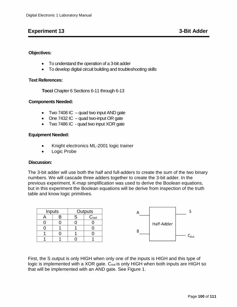
Digital Electronic 1 Laboratory Manual
Experiment 13 3-Bit Adder
Objectives:
• To understand the operation of a 3-bit adder • To develop digital circuit building and troubleshooting skills
Text References: Tocci Chapter 6 Sections 6-11 through 6-13
Components Needed:
• Two 7408 IC – quad two input AND gate • One 7432 IC – quad two-input OR gate • Two 7486 IC - quad two input XOR gate
Equipment Needed:
• Knight electronics ML-2001 logic trainer • Logic Probe
Discussion:
The 3-bit adder will use both the half and full-adders to create the sum of the two binary numbers. We will cascade three adders together to create the 3-bit adder. In the previous experiment, K-map simplification was used to derive the Boolean equations, but in this experiment the Boolean equations will be derive from inspection of the truth table and know logic primitives.
First, the S output is only HIGH when only one of the inputs is HIGH and this type of logic is implemented with a XOR gate. Cout is only HIGH when both inputs are HIGH so that will be implemented with an AND gate. See Figure 1.
Inputs Outputs A B S Cout 0 0 0 0 0 1 1 0 1 0 1 0 1 1 0 1
Page 100 of 111
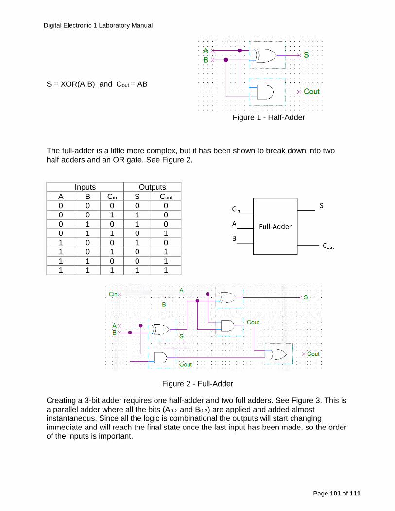
Digital Electronic 1 Laboratory Manual
S = XOR(A,B) and Cout = AB
Figure 1 - Half-Adder
The full-adder is a little more complex, but it has been shown to break down into two half adders and an OR gate. See Figure 2.
Figure 2 - Full-Adder
Creating a 3-bit adder requires one half-adder and two full adders. See Figure 3. This is a parallel adder where all the bits (A0-2 and B0-2) are applied and added almost instantaneous. Since all the logic is combinational the outputs will start changing immediate and will reach the final state once the last input has been made, so the order of the inputs is important.
Inputs Outputs A B Cin S Cout 0 0 0 0 0 0 0 1 1 0 0 1 0 1 0 0 1 1 0 1 1 0 0 1 0 1 0 1 0 1 1 1 0 0 1 1 1 1 1 1
Page 101 of 111
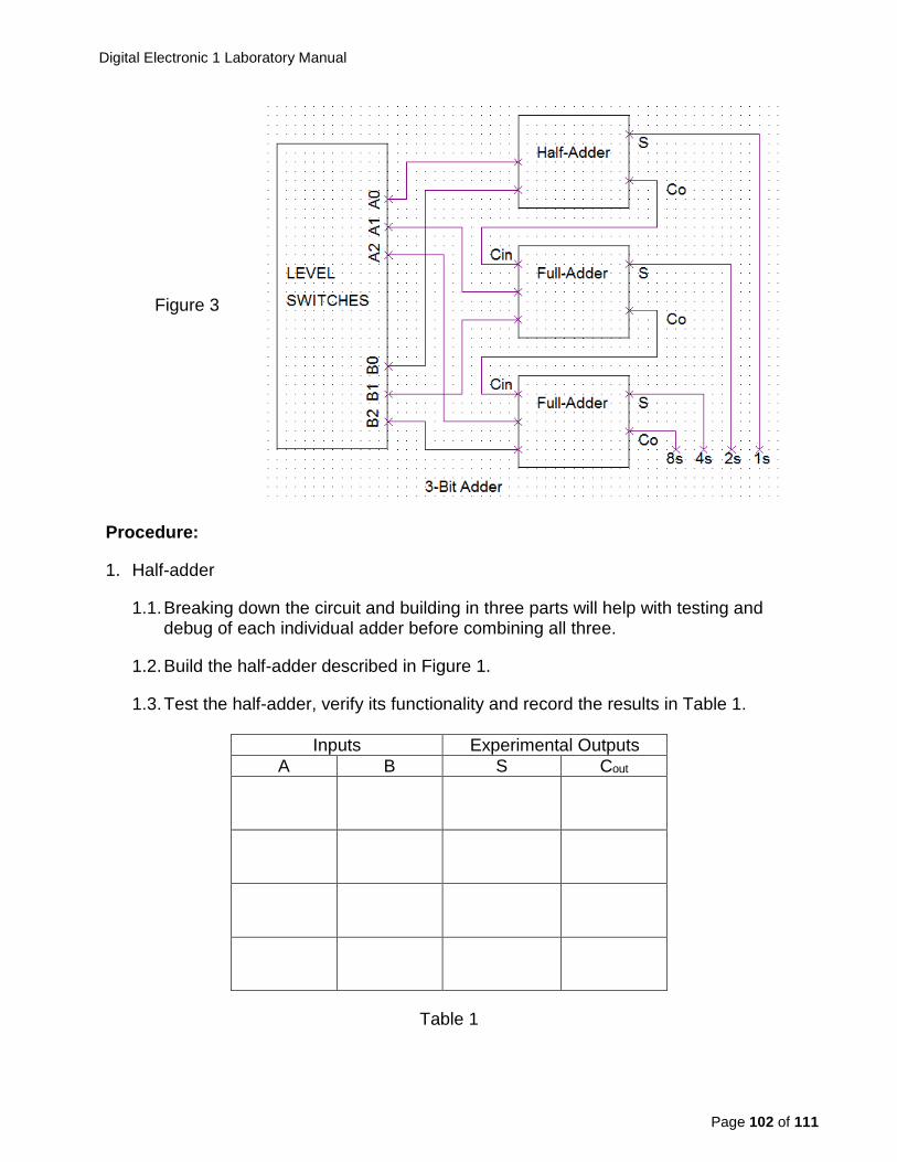
Digital Electronic 1 Laboratory Manual
Figure 3
Procedure:
1. Half-adder
1.1. Breaking down the circuit and building in three parts will help with testing and debug of each individual adder before combining all three.
1.2. Build the half-adder described in Figure 1.
1.3. Test the half-adder, verify its functionality and record the results in Table 1.
Inputs Experimental Outputs A B S Cout
Table 1
Page 102 of 111

Digital Electronic 1 Laboratory Manual
2. Full-adders
2.1. Build each full-adder as described in Figure 2. Do not connect the two full-adder together.
2.2. Test each full-adder separately, verify its functionality and record the results in Table 2 and 3.
Fuller-Adder #1
Inputs Outputs A B Cin S Cout
Table 2 Table 3
3. Integration
3.1. Make the connections between the half-adder and the two full-adder.
3.2. Test the 3-bit adder, verify its functionality and record the results in Table 4. The far left columns in each section are the decimal equivalent of the binary input or binary output. Remember that the order of the inputs is important so use trial and error to learn the best approach for order of inputs.
Fuller-Adder #2 Inputs Outputs
A B Cin S Cout
Page 103 of 111
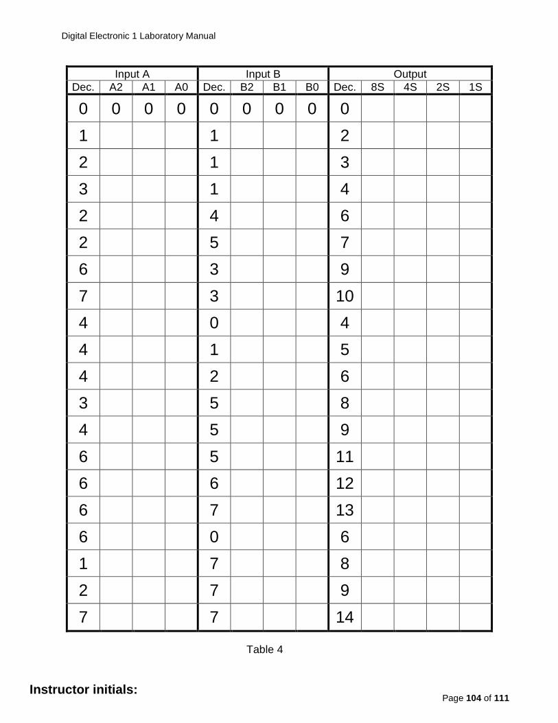
Digital Electronic 1 Laboratory Manual
Input A Input B Output Dec. A2 A1 A0 Dec. B2 B1 B0 Dec. 8S 4S 2S 1S
0 0 0 0 0 0 0 0 0 1 1 2 2 1 3 3 1 4 2 4 6 2 5 7 6 3 9 7 3 10 4 0 4 4 1 5 4 2 6 3 5 8 4 5 9 6 5 11 6 6 12 6 7 13 6 0 6 1 7 8 2 7 9 7 7 14
Table 4
Instructor initials: Page 104 of 111

Digital Electronic 1 Laboratory Manual
Questions:
1. What is the highest binary sum that this 3-bit adder can produce? What’s the decimal equivalent?
2. What is the inherent problem with this type of adder? Hint: Think of the ripple counter.
3. How does this 3-bit adder response when adding two number and a mistake was made in one switch? The change to the correct value would come after the two values were input. For example, adding 5 + 3 but by mistake 5 + 2 was entered via the switches and then changed a second later to 5 + 3.
4. What were some of the issues and challenges that you encountered during this experiment?
Page 105 of 111

Digital Electronic 1 Laboratory Manual
Experiment 14 Design a Asynchronous Counter
Objectives:
• To understand the operation of an asynchronous counter • To implement a mod-10 circuit to an asynchronous counter • To develop digital circuit building and troubleshooting skills
Text References: Tocci Chapter 7 Sections 7-1 through 7-4
Components Needed:
• One 7400 IC – Quadruple 2-input NAND gate • One 7476 IC – Dual J-K flip-flops
Equipment Needed:
• Knight electronics ML-2001 logic trainer • Logic Probe
Discussion:
A ripple or asynchronous counter is a counter which only the first flip-flop (FF0) is connected to the external clock. The remaining flip-flops are triggered by the falling edge of the output Q of the previous flip-flop. Because of the inherent propagation delay through a flip-flop, the transition of the input clock pulse and a transition of the Q output of a flip-flop can never occur at exactly the same time. Since the flip-flops cannot be triggered simultaneously the counter ends up producing an asynchronous operation. The clock pulse fed into FF0 is rippled through the other counters after the propagation delays (like a ripple on water) hence the name Ripple Counter. The J-K flip-flops are configured in the toggle mode which allows the flip-flop to change states or toggle on every negative going clock pulse.
Figure 1 is an example of a 4-bit ripple counter and therefore it has four flip-flops and 16 different states (24 = 16). This 4-bit ripple counter is also known as a mod-16 counter for its 16 different states. The mod or modulo number reflects the number of states in the counter.
Another type of counter is the synchronous counter and it eliminates the delay effect that is present with the asynchronous counters. The clock is connected directly to the CLK input of each flip-flop so the outputs change together or synchronously. A synchronous counter does require more circuitry, but in high speed applications the ripple counter delay will be unacceptable.
Page 106 of 111

Digital Electronic 1 Laboratory Manual
Figure 1
Procedure:
1. Asynchronous Up Counter
1.1. Prelab: Use Figure 1, the pertinent datasheets and the textbook to design the 4-bit asynchronous counter. Sketch it out on paper and then design the counter in MultiSim. Bring both the sketch and MultiSim to lab for full credit.
1.2. Build the circuit from the MultiSim design. Use the Pulser Switches to act as the clock input.
1.3. Draw the output of the four LEDs for the first 11 clock pulses in Figure 2.
CLK 1 2 3 4 5 6 7 8 9 10 11
D
C
B
A
Figure 2
2. Asynchronous Down Counter
2.1. Describe how this counter be converted to count down? Do not tear down the up counter!
Page 107 of 111

Digital Electronic 1 Laboratory Manual
2.2. Make the changes to the MultiSim design which would make the circuit a down counter.
2.3. Build modify the circuit to become a down counter.
2.4. Draw the output of the four LEDs for the first 11 clock pulses Figure 3.
CLK 1 2 3 4 5 6 7 8 9 10 11
D
C
B
A
Figure 3
3. Mod-10 Counter
3.1. Convert the down counter back to an up counter and verify is functional.
3.2. Design the circuitry needed to make the up counter a mod-10 counter. Make the changes to MultiSim.
3.3. Build modify the circuit to become a mod-10 counter.
3.4. Draw the output of the four LEDs for the first 11 clock pulses Figure 4.
CLK 1 2 3 4 5 6 7 8 9 10 11
D
C
B
A
Figure 4
Instructor initials: Page 108 of 111

Digital Electronic 1 Laboratory Manual
Questions:
1. After watching how the asynchronous counter works what is the major disadvantage of this type of counter compared to a synchronous counter?
2. Draw the circuitry needed for a mod-8 counter.
3. Which LED is the MSB?
4. How does the duty cycle change from the clock input for each FF?
5. Describe or sketch the circuitry needed to shut off all the LED at once.
Page 109 of 111

Digital Electronic 1 Laboratory Manual
Appendix A: Experiment Grading Sheet
Page 110 of 111

Digital Electronic 1 Laboratory Manual
Experiment Grading Sheet Course:_________________________
Name: ___________________________________________ Date: _____________
Partner: ______________________________________________________________
Experiment: __________________________________________________________
Grading Element Maximum Points
Points Earned
Objective 10
Discussion 20
Conclusion 20
Data/Graphs/Diagrams 20
Calculations/Questions 20
Neatness/Spelling/Grammar 10
Total 100 Comments: ______________________________________________________________________
______________________________________________________________________
______________________________________________________________________
______________________________________________________________________
Instructor:___________________________________
Page 111 of 111


![EC1204 Digital Electronics Laboratory Manual REC[1]](https://img.pdfslide.net/doc/110x75/55cf9cf4550346d033aba616/ec1204-digital-electronics-laboratory-manual-rec1.jpg)


![EC1258- Digital Electronics Laboratory Manual [REC]](https://img.pdfslide.net/doc/110x75/5465ea8cb4af9fc23a8b46e7/ec1258-digital-electronics-laboratory-manual-rec.jpg)