Embed Size (px)
Citation preview
MAE 511
EXPERIMENTAL METHODS I
DIGITAL SAMPLING OSCILLOSCOPE
Madeline S. Vorenkamp
Claudia E. Brunner
Guided By - Prof. Michael Littman and Jon Prevost
Department of Mechanical and Aerospace Engineering
Princeton University
1
MAE 511: EXPERIMENTAL METHODS I DIGITAL SAMPLING OSCILLOSCOPE
Contents
1 Introduction 3
2 Digital Sampling Oscilloscope Design 4
2.1 Front End . . . . . . . . . . . . . . . . . . . . . . . . . . . . . . . . . 4
2.2 Analog to Digital Converter . . . . . . . . . . . . . . . . . . . . . . 7
2.3 Tri-State . . . . . . . . . . . . . . . . . . . . . . . . . . . . . . . . 9
2.4 Memory . . . . . . . . . . . . . . . . . . . . . . . . . . . . . . . . 10
2.5 Counter . . . . . . . . . . . . . . . . . . . . . . . . . . . . . . . . . 12
2.6 Digital to Analog Converter . . . . . . . . . . . . . . . . . . . . . 13
2.7 Teensy . . . . . . . . . . . . . . . . . . . . . . . . . . . . . . . . . . 14
3 Results 16
4 Conclusion 18
5 Appendix 19
5.1 Components . . . . . . . . . . . . . . . . . . . . . . . . . . . . . . 19
5.2 Teensy Code . . . . . . . . . . . . . . . . . . . . . . . . . . . . . . 20
5.3 Front End Schematic . . . . . . . . . . . . . . . . . . . . . . . . . 23
5.4 Body Schematic . . . . . . . . . . . . . . . . . . . . . . . . . . . . . 24
Page 2 of 24
MAE 511: EXPERIMENTAL METHODS I DIGITAL SAMPLING OSCILLOSCOPE
1 Introduction
This paper presents a design for a breadboard based digital sampling oscil-
loscope, DSO. A digital sampling oscilloscope is a device used to display an
electrical signal varying in time. Unlike a voltmeter which displays a time-
averaged voltage, an oscilloscope plots the voltage contours such that the
waveform’s amplitude, frequency, noise and other properties are easily in-
terpreted and can then be further analyzed. In order to display an electrical
signal varying in time, the DSO captures a voltage signal from a voltage source,
i.e. a signal generator. The voltage signal is then written to memory, which is
then read by a micro-controller, i.e. a Teensy. The micro-controller then sends
the analog waveform to a computer for display. Our design is more similar
to a digitizer than a traditional modern oscilloscope in that the display is not
integrated in the breadboard and is instead a computer program which plots
the stored signal from the DSO’s memory.
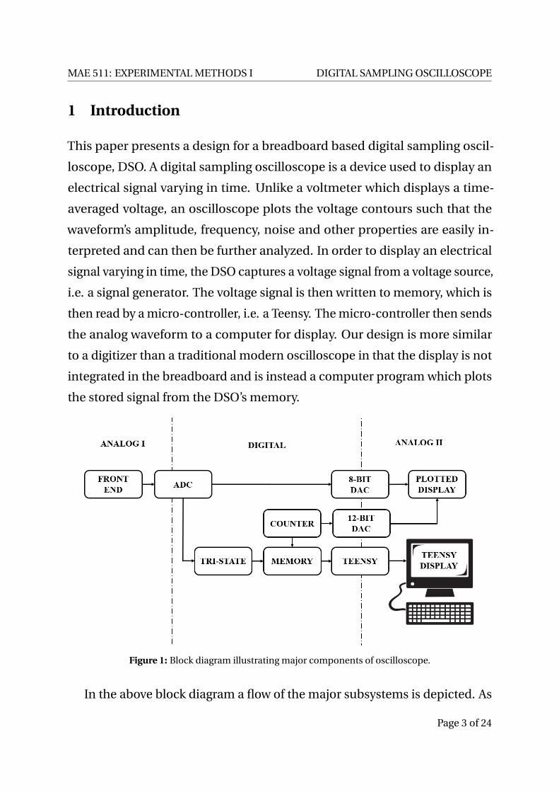
Figure 1: Block diagram illustrating major components of oscilloscope.
In the above block diagram a flow of the major subsystems is depicted. As
Page 3 of 24
MAE 511: EXPERIMENTAL METHODS I DIGITAL SAMPLING OSCILLOSCOPE
is shown in the diagram, the DSO can be broken into three regimes, Analog I,
Digital, and Analog II. In the first analog regime an input voltage is modified
by the front end and sent to the analog-to-digital converter, ADC. The ADC
serves as the interface between the first analog regime and the digital regime.
In the digital regime the ADC sends a digital signal through the tri-state to
the memory in which the storage location is advanced via the counter. The
values from the ADC are sent to the 8-bit digital to analog converter, DAC,
and the addresses of the memory are sent to the 12-bit DAC. The DAC’s serve
as the interface from the digital regime to the second analog regime. These
analog outputs could be plotted as a waveform. However, the micro-controller
instead reads directly from the memory and sends the waveform data to the
computer for display.
In the sections that follow the design of the DSO will be discusses by
component. The design of the DSO will be followed by a results section
and then by a conclusions section.
2 Digital Sampling Oscilloscope Design
In this section an overview of each subsystem’s functionality and the manner
in which these subsystems relate to one another will be presented.
2.1 Front End
The front end of the DSO consists of three operational amplifiers, op-amps,
which serve to convert an input voltage signal ranging from -5V to +5V to a
scaled signal ranging from 0 to +5V. This is done to protect the ADC which
requires a unipolar voltage input with a maximum of +5V volts.
Page 4 of 24
MAE 511: EXPERIMENTAL METHODS I DIGITAL SAMPLING OSCILLOSCOPE
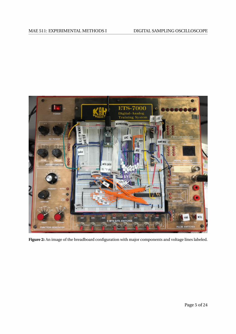
Figure 2: An image of the breadboard configuration with major components and voltage lines labeled.
Page 5 of 24
MAE 511: EXPERIMENTAL METHODS I DIGITAL SAMPLING OSCILLOSCOPE
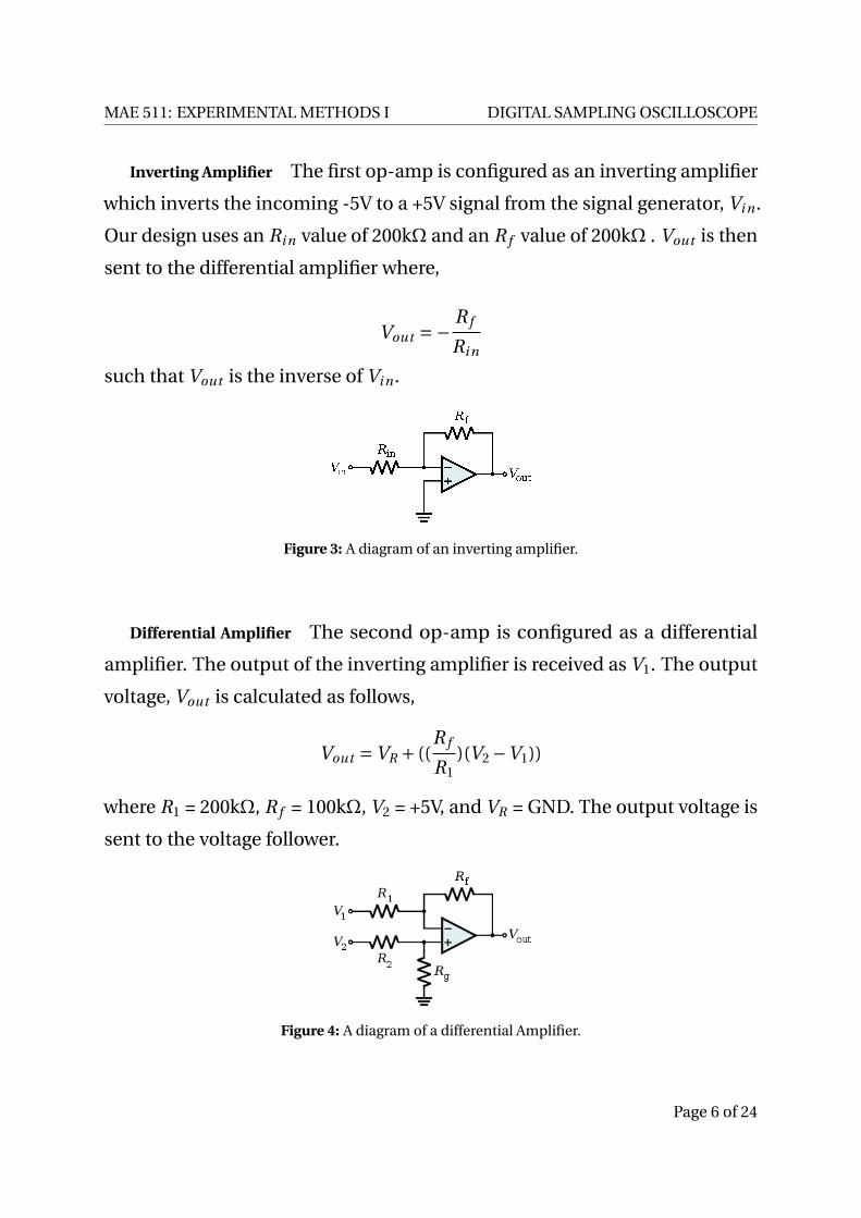
Inverting Amplifier The first op-amp is configured as an inverting amplifier
which inverts the incoming -5V to a +5V signal from the signal generator, Vi n.
Our design uses an Ri n value of 200kΩ and an R f value of 200kΩ . Vout is then
sent to the differential amplifier where,
Vout =− R f
Ri n
such that Vout is the inverse of Vi n.
Figure 3: A diagram of an inverting amplifier.
Differential Amplifier The second op-amp is configured as a differential
amplifier. The output of the inverting amplifier is received as V1. The output
voltage, Vout is calculated as follows,
Vout =VR + ((R f
R1)(V2 −V1))
where R1 = 200kΩ, R f = 100kΩ, V2 = +5V, and VR = GND. The output voltage is
sent to the voltage follower.
Figure 4: A diagram of a differential Amplifier.
Page 6 of 24

MAE 511: EXPERIMENTAL METHODS I DIGITAL SAMPLING OSCILLOSCOPE
Voltage Follower The third op-amp is configured as a voltage follower. This
serves to ensure that the output of the op-amp matches its input (Vout =Vi n).
The output voltage is then sent to the analog-to-digital converter.
Figure 5: A diagram of a voltage follower.
Figure 6: An image of (1) the input signal from-5V to +5V, (2) the signal inverted by the invertingamplifier and (3) the signal inverted and scaled from 0V to +5V by the differential amplifier (to be sentthrough a voltage follower to the Analog to Digital converter).
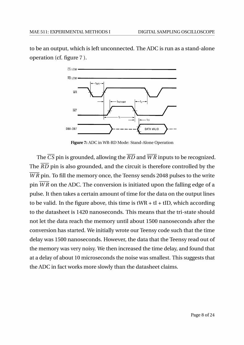
2.2 Analog to Digital Converter
The ADC0820 is a high-speed 8-bit analog-to-digital converter with a built in
sample-and-hold function. It receives an analog unipolar 0-5 V input from the
front end to its VI N pin, and converts it to an 8-bit digital signal. The MODE
pin is pulled high, setting the ADC to WR-RD mode. This causes the INT pin
Page 7 of 24
MAE 511: EXPERIMENTAL METHODS I DIGITAL SAMPLING OSCILLOSCOPE
to be an output, which is left unconnected. The ADC is run as a stand-alone
operation (cf. figure 7 ).
Figure 7: ADC in WR-RD Mode: Stand-Alone Operation
The C S pin is grounded, allowing the RD and W R inputs to be recognized.
The RD pin is also grounded, and the circuit is therefore controlled by the
W R pin. To fill the memory once, the Teensy sends 2048 pulses to the write
pin W R on the ADC. The conversion is initiated upon the falling edge of a
pulse. It then takes a certain amount of time for the data on the output lines
to be valid. In the figure above, this time is tWR + tI + tID, which according
to the datasheet is 1420 nanoseconds. This means that the tri-state should
not let the data reach the memory until about 1500 nanoseconds after the
conversion has started. We initially wrote our Teensy code such that the time
delay was 1500 nanoseconds. However, the data that the Teensy read out of
the memory was very noisy. We then increased the time delay, and found that
at a delay of about 10 microseconds the noise was smallest. This suggests that
the ADC in fact works more slowly than the datasheet claims.
Page 8 of 24
MAE 511: EXPERIMENTAL METHODS I DIGITAL SAMPLING OSCILLOSCOPE
2.3 Tri-State
The tri-state (SN74LS244) controls the data lines running from the ADC to the
memory. Each data line from the ADC is connected to an A (input) pin on the
tri-state, and the corresponding Y (output) pin is connected to the memory.
In this circuit, the tri-state has two functions. First, it ensures that the ADC
and the memory do not simultaneously write to the same lines, since this can
damage the parts, and inhibits their functionality. The tri-state thus acts as a
buffer between the ADC and the memory. The ADC continuously converts
data and outputs it to its data lines (purple wires), so in order for the Teensy
to read data out of the memory, the tri-state must disconnect the ADC data
lines from the memory data lines (white wires). The tri-state is controlled via
the gate pins 1G and 2G . While the Teensy reads data out of the memory, it
keeps the gates high, so that the ADC is disconnected from the memory.
During write mode, when the data from the ADC is being saved to the
memory, the tri-state serves another purpose: after the ADC receives a pulse
from the Teensy to its W R pin, it takes a certain amount of time for the data
conversion to be completed and the output pins to be stable (cf. section
2.2). Preventing the data from the ADC from reaching the memory until
the conversion is complete ensures that the data saved to the memory is
correct. We thus want the tri-state gates to open a certain time after the ADC
conversion began. We determined this time-frame to be 10 microseconds,
and wrote the Teensy code such that the tri-state gates receive a pulse 10
microseconds after the ADC receives a pulse. The ADC conversion is started
on the falling edge of a pulse, and the tri-state gates open on the falling edge
of a pulse, so by the time the data reaches the memory, the conversion is
completed and the data is valid.
Page 9 of 24
MAE 511: EXPERIMENTAL METHODS I DIGITAL SAMPLING OSCILLOSCOPE
Table 1: Truth Table for SRAM
Mode C S OE W E
Standby LOW HIGH HIGHRead LOW LOW HIGHWrite LOW HIGH LOW
2.4 Memory
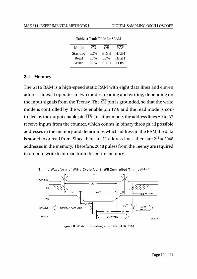
The 6116 RAM is a high-speed static RAM with eight data lines and eleven
address lines. It operates in two modes, reading and writing, depending on
the input signals from the Teensy. The C S pin is grounded, so that the write
mode is controlled by the write enable pin W E and the read mode is con-
trolled by the output enable pin OE . In either mode, the address lines A0 to A7
receive inputs from the counter, which counts in binary through all possible
addresses in the memory and determines which address in the RAM the data
is stored to or read from. Since there are 11 address lines, there are 211 = 2048
addresses in the memory. Therefore, 2048 pulses from the Teensy are required
in order to write to or read from the entire memory.
Figure 8: Write timing diagram of the 6116 RAM.
Page 10 of 24
MAE 511: EXPERIMENTAL METHODS I DIGITAL SAMPLING OSCILLOSCOPE
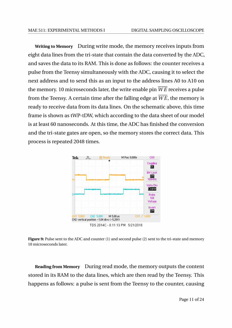
Writing to Memory During write mode, the memory receives inputs from
eight data lines from the tri-state that contain the data converted by the ADC,
and saves the data to its RAM. This is done as follows: the counter receives a
pulse from the Teensy simultaneously with the ADC, causing it to select the
next address and to send this as an input to the address lines A0 to A10 on
the memory. 10 microseconds later, the write enable pin W E receives a pulse
from the Teensy. A certain time after the falling edge at W E , the memory is
ready to receive data from its data lines. On the schematic above, this time
frame is shown as tWP-tDW, which according to the data sheet of our model
is at least 60 nanoseconds. At this time, the ADC has finished the conversion
and the tri-state gates are open, so the memory stores the correct data. This
process is repeated 2048 times.
Figure 9: Pulse sent to the ADC and counter (1) and second pulse (2) sent to the tri-state and memory10 microseconds later.
Reading from Memory During read mode, the memory outputs the content
stored in its RAM to the data lines, which are then read by the Teensy. This
happens as follows: a pulse is sent from the Teensy to the counter, causing
Page 11 of 24
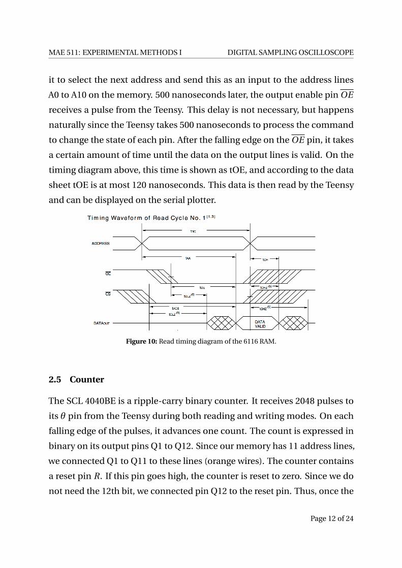
MAE 511: EXPERIMENTAL METHODS I DIGITAL SAMPLING OSCILLOSCOPE
it to select the next address and send this as an input to the address lines
A0 to A10 on the memory. 500 nanoseconds later, the output enable pin OE
receives a pulse from the Teensy. This delay is not necessary, but happens
naturally since the Teensy takes 500 nanoseconds to process the command
to change the state of each pin. After the falling edge on the OE pin, it takes
a certain amount of time until the data on the output lines is valid. On the
timing diagram above, this time is shown as tOE, and according to the data
sheet tOE is at most 120 nanoseconds. This data is then read by the Teensy
and can be displayed on the serial plotter.
Figure 10: Read timing diagram of the 6116 RAM.
2.5 Counter
The SCL 4040BE is a ripple-carry binary counter. It receives 2048 pulses to
its θ pin from the Teensy during both reading and writing modes. On each
falling edge of the pulses, it advances one count. The count is expressed in
binary on its output pins Q1 to Q12. Since our memory has 11 address lines,
we connected Q1 to Q11 to these lines (orange wires). The counter contains
a reset pin R. If this pin goes high, the counter is reset to zero. Since we do
not need the 12th bit, we connected pin Q12 to the reset pin. Thus, once the
Page 12 of 24
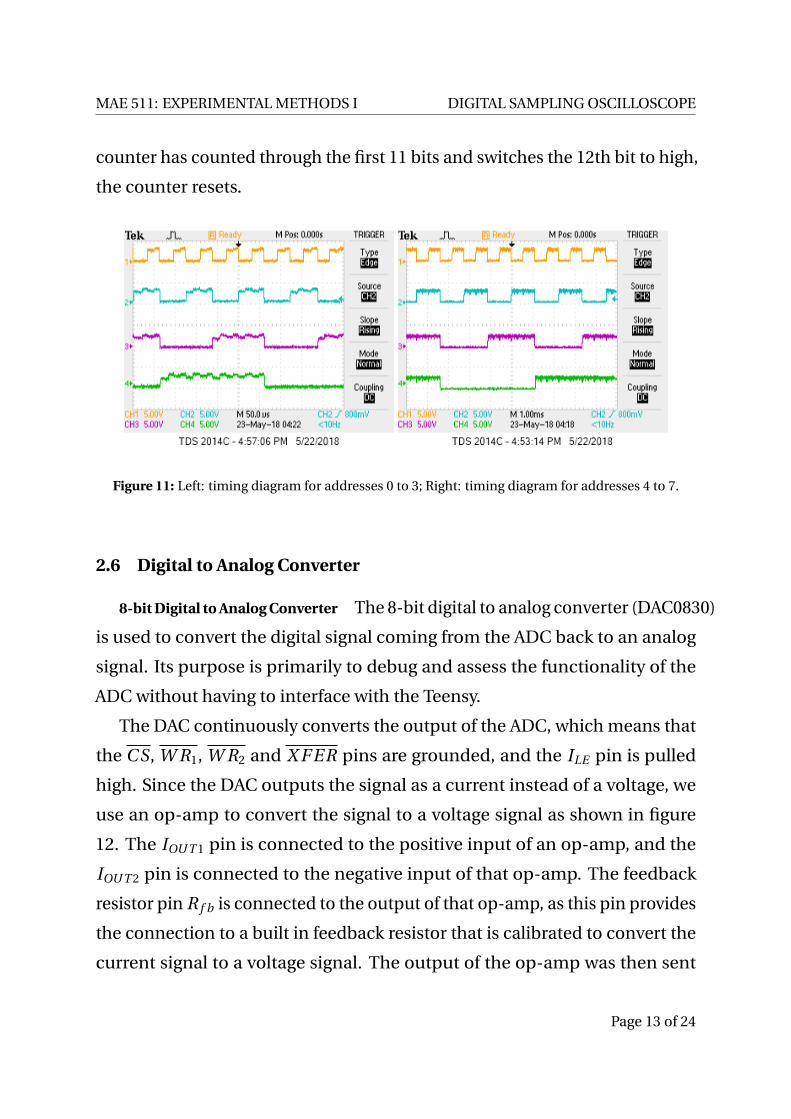
MAE 511: EXPERIMENTAL METHODS I DIGITAL SAMPLING OSCILLOSCOPE
counter has counted through the first 11 bits and switches the 12th bit to high,
the counter resets.
Figure 11: Left: timing diagram for addresses 0 to 3; Right: timing diagram for addresses 4 to 7.
2.6 Digital to Analog Converter
8-bit Digital to Analog Converter The 8-bit digital to analog converter (DAC0830)
is used to convert the digital signal coming from the ADC back to an analog
signal. Its purpose is primarily to debug and assess the functionality of the
ADC without having to interface with the Teensy.
The DAC continuously converts the output of the ADC, which means that
the C S, W R1, W R2 and X F ER pins are grounded, and the ILE pin is pulled
high. Since the DAC outputs the signal as a current instead of a voltage, we
use an op-amp to convert the signal to a voltage signal as shown in figure
12. The IOU T 1 pin is connected to the positive input of an op-amp, and the
IOU T 2 pin is connected to the negative input of that op-amp. The feedback
resistor pin R f b is connected to the output of that op-amp, as this pin provides
the connection to a built in feedback resistor that is calibrated to convert the
current signal to a voltage signal. The output of the op-amp was then sent
Page 13 of 24
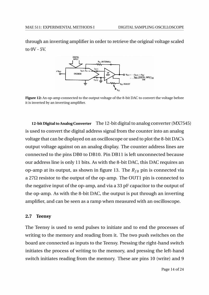
MAE 511: EXPERIMENTAL METHODS I DIGITAL SAMPLING OSCILLOSCOPE
through an inverting amplifier in order to retrieve the original voltage scaled
to 0V - 5V.
Figure 12: An op-amp connected to the output voltage of the 8-bit DAC to convert the voltage beforeit is inverted by an inverting amplifier.
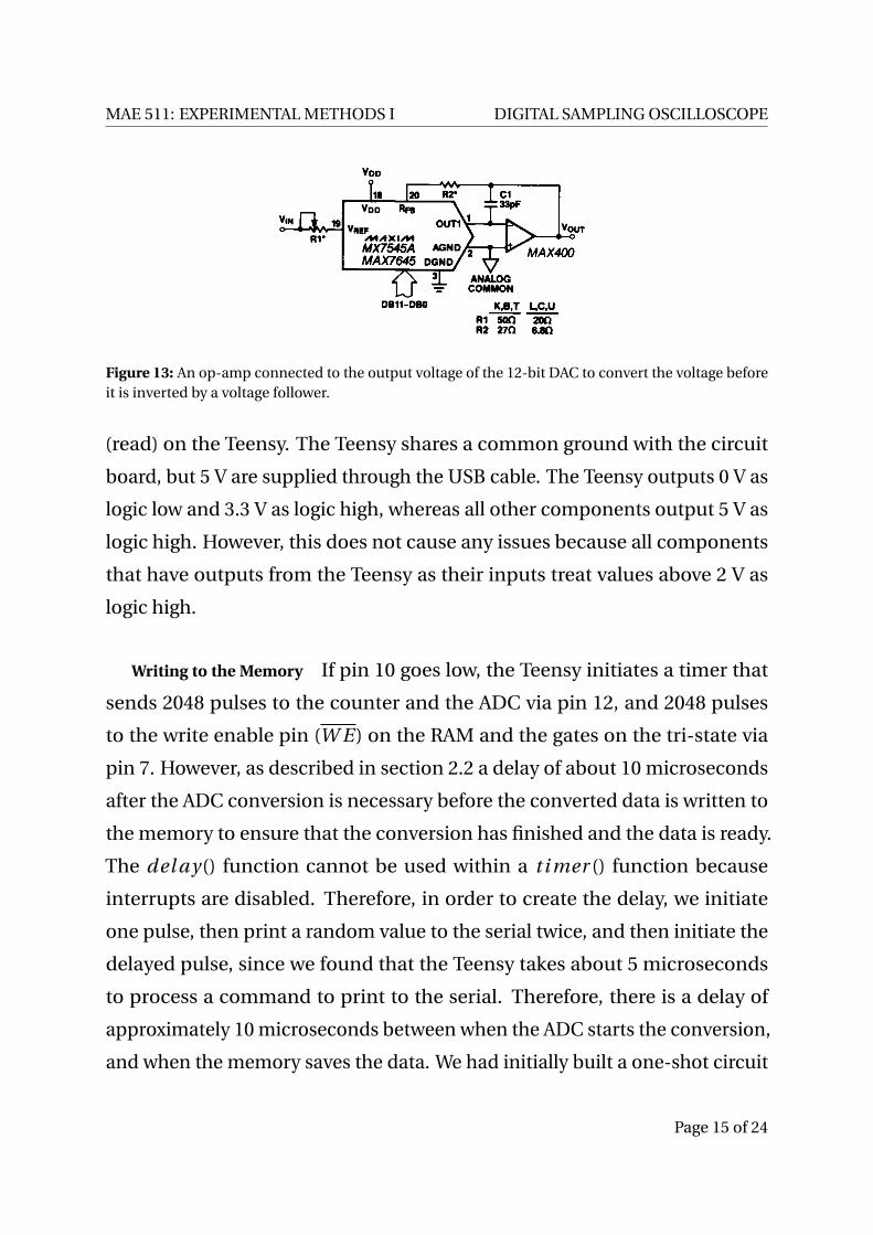
12-bit Digital to Analog Converter The 12-bit digital to analog converter (MX7545)
is used to convert the digital address signal from the counter into an analog
voltage that can be displayed on an oscilloscope or used to plot the 8-bit DAC’s
output voltage against on an analog display. The counter address lines are
connected to the pins DB0 to DB10. Pin DB11 is left unconnected because
our address line is only 11 bits. As with the 8-bit DAC, this DAC requires an
op-amp at its output, as shown in figure 13. The R f B pin is connected via
a 27Ω resistor to the output of the op-amp. The OUT1 pin is connected to
the negative input of the op-amp, and via a 33 pF capacitor to the output of
the op-amp. As with the 8-bit DAC, the output is put through an inverting
amplifier, and can be seen as a ramp when measured with an oscilloscope.
2.7 Teensy
The Teensy is used to send pulses to initiate and to end the processes of
writing to the memory and reading from it. The two push switches on the
board are connected as inputs to the Teensy. Pressing the right-hand switch
initiates the process of writing to the memory, and pressing the left-hand
switch initiates reading from the memory. These are pins 10 (write) and 9
Page 14 of 24
MAE 511: EXPERIMENTAL METHODS I DIGITAL SAMPLING OSCILLOSCOPE
Figure 13: An op-amp connected to the output voltage of the 12-bit DAC to convert the voltage beforeit is inverted by a voltage follower.
(read) on the Teensy. The Teensy shares a common ground with the circuit
board, but 5 V are supplied through the USB cable. The Teensy outputs 0 V as
logic low and 3.3 V as logic high, whereas all other components output 5 V as
logic high. However, this does not cause any issues because all components
that have outputs from the Teensy as their inputs treat values above 2 V as
logic high.
Writing to the Memory If pin 10 goes low, the Teensy initiates a timer that
sends 2048 pulses to the counter and the ADC via pin 12, and 2048 pulses
to the write enable pin (W E) on the RAM and the gates on the tri-state via
pin 7. However, as described in section 2.2 a delay of about 10 microseconds
after the ADC conversion is necessary before the converted data is written to
the memory to ensure that the conversion has finished and the data is ready.
The del ay() function cannot be used within a t i mer () function because
interrupts are disabled. Therefore, in order to create the delay, we initiate
one pulse, then print a random value to the serial twice, and then initiate the
delayed pulse, since we found that the Teensy takes about 5 microseconds
to process a command to print to the serial. Therefore, there is a delay of
approximately 10 microseconds between when the ADC starts the conversion,
and when the memory saves the data. We had initially built a one-shot circuit
Page 15 of 24
MAE 511: EXPERIMENTAL METHODS I DIGITAL SAMPLING OSCILLOSCOPE
to create this delay, but then realized that our code could easily generate a
sufficient delay.
The time between each pulse is 55 microseconds. This means that our
sampling frequency is about 18 kHz. However, the sampling frequency can
easily be adjusted in the Teensy code.
Reading from the Memory If pin 9 goes low, the Teensy initiates a timer that
sends 2048 pulses to the counter and the ADC via pin 12, and the same num-
ber of pulses to the output enable pin (OE) on the RAM via pin 8. Since the
commands are written consecutively in the code, there is a 500 nanosecond
delay between the pulses. The pulses to the ADC are not necessary for func-
tionality. The ADC continues to convert data, but the gates of the tri-state are
held high by pin 7 on the Teensy. Thus, the data outputs of the ADC (purple
lines) are not let through the tri-state, and the memory controls the data lines
(white wires). These data lines then run to pins 14 to 21 on the Teensy. The
Teensy then reads the inputs from these data lines as bits, and stores them in
a byte. This byte captures the voltage, where the values are scaled such that
the input of ±5 V is expressed on a scale from 0 to 255.
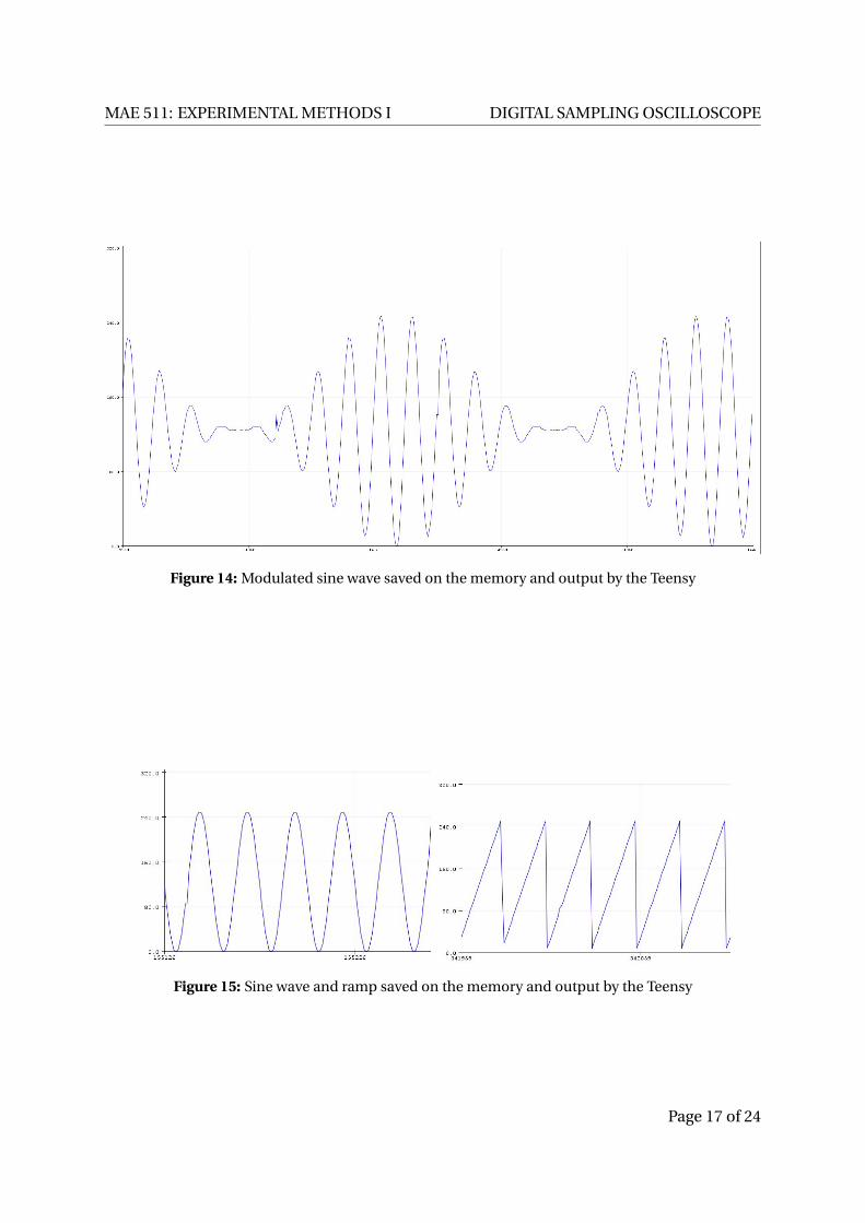
3 Results
We used the serial plotter in the Teensy software to visualize the data that the
Teensy reads out of the memory. Plots of different voltage signals are shown
in figures 14 and 15. As mentioned in section 2.7, our results were initially
very noisy, and we had to increase the delay between the data conversion
in the ADC and the data storage by the RAM in order to reduce noise in the
signal. The voltage is plotted on a scale from 0 to 255, since this represents
the range of bytes that can be represented with 8 bits, so scaling this range to
±10V would retrieve the original voltages.
Page 16 of 24
MAE 511: EXPERIMENTAL METHODS I DIGITAL SAMPLING OSCILLOSCOPE
Figure 14: Modulated sine wave saved on the memory and output by the Teensy
Figure 15: Sine wave and ramp saved on the memory and output by the Teensy
Page 17 of 24
MAE 511: EXPERIMENTAL METHODS I DIGITAL SAMPLING OSCILLOSCOPE
4 Conclusion
Our design produced a fully functional digital sampling oscilloscope. We were
tasked with storing and retrieving a -5 V to 5 V input signal. Our oscilloscope
was able to convert the analog input voltage to a digital voltage, write the
digital data to the memory, read the digital data from the memory, convert
the digital data to analog data, and display the analog data. The signal was
returned via a Teensy micro-controller and displayed on the serial plotter
from the Teensy software package.
Throughout the course of the project we learned a lot more than just
how to build a breadboard DSO. We learned how to design a breadboard
DSO. We did everything from reading and interpreting data sheets to trouble
shooting timing errors. By successfully completing these tasks and producing
the functional breadboard DSO we were able to demonstrate fundamental
levels of understanding in basic electronic techniques, digital electronics,
data acquisition, and data analysis.
Page 18 of 24
MAE 511: EXPERIMENTAL METHODS I DIGITAL SAMPLING OSCILLOSCOPE
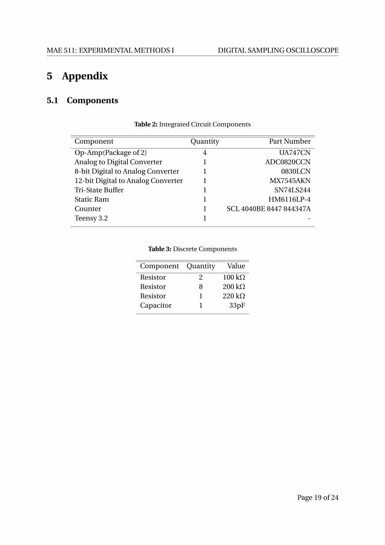
5 Appendix
5.1 Components
Table 2: Integrated Circuit Components
Component Quantity Part Number
Op-Amp(Package of 2) 4 UA747CNAnalog to Digital Converter 1 ADC0820CCN8-bit Digital to Analog Converter 1 0830LCN12-bit Digital to Analog Converter 1 MX7545AKNTri-State Buffer 1 SN74LS244Static Ram 1 HM6116LP-4Counter 1 SCL 4040BE 8447 844347ATeensy 3.2 1 -
Table 3: Discrete Components
Component Quantity Value
Resistor 2 100 kΩResistor 8 200 kΩResistor 1 220 kΩCapacitor 1 33pF
Page 19 of 24
MAE 511: EXPERIMENTAL METHODS I DIGITAL SAMPLING OSCILLOSCOPE
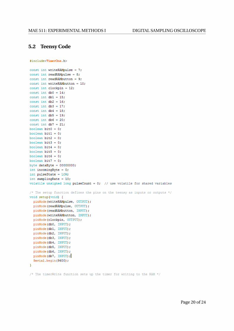
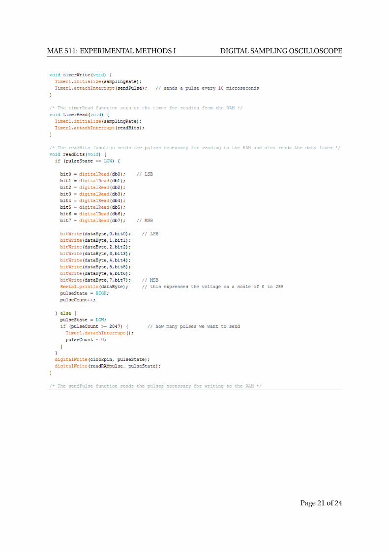
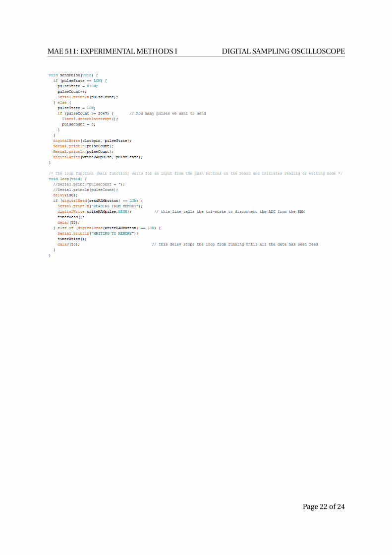
5.2 Teensy Code
Page 20 of 24
MAE 511: EXPERIMENTAL METHODS I DIGITAL SAMPLING OSCILLOSCOPE
Page 21 of 24
MAE 511: EXPERIMENTAL METHODS I DIGITAL SAMPLING OSCILLOSCOPE
Page 22 of 24
MAE 511: EXPERIMENTAL METHODS I DIGITAL SAMPLING OSCILLOSCOPE
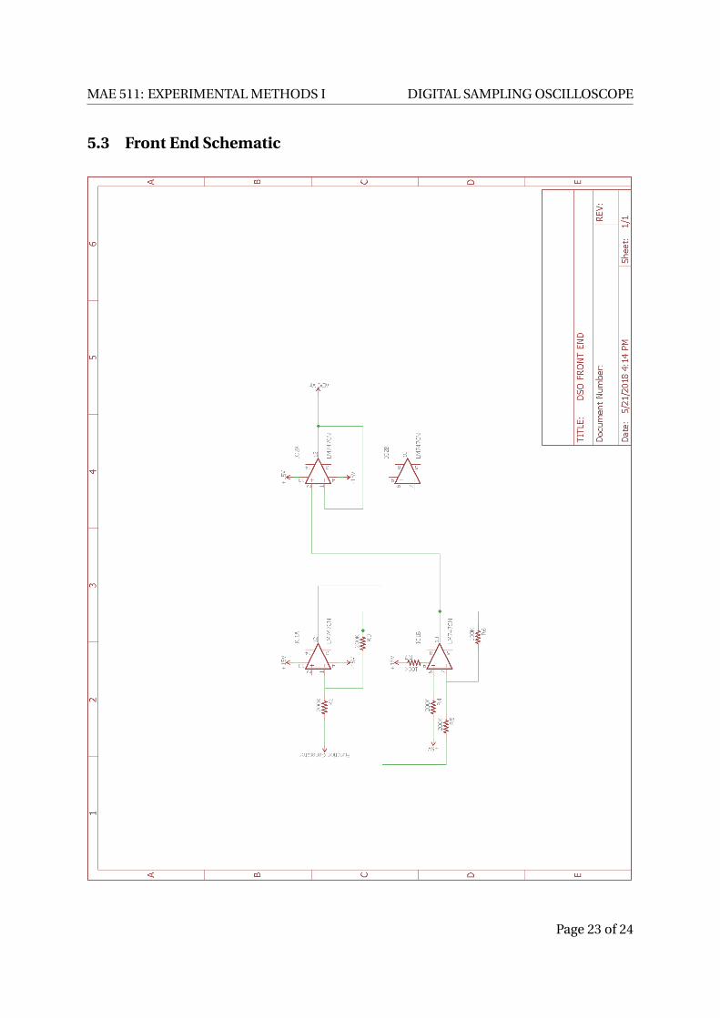
5.3 Front End Schematic
Page 23 of 24
MAE 511: EXPERIMENTAL METHODS I DIGITAL SAMPLING OSCILLOSCOPE
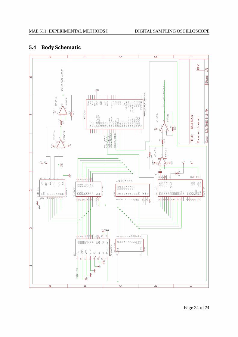
5.4 Body Schematic
Page 24 of 24