Embed Size (px)
Citation preview
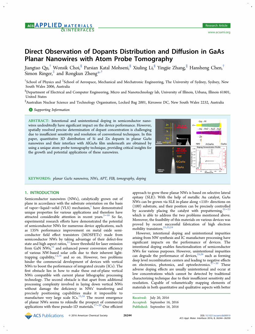
Direct Observation of Dopants Distribution and Diffusion in GaAsPlanar Nanowires with Atom Probe TomographyJiangtao Qu,† Wonsik Choi,§ Parsian Katal Mohseni,§ Xiuling Li,§ Yingjie Zhang,∥ Hansheng Chen,†
Simon Ringer,‡ and Rongkun Zheng*,†
†School of Physics and ‡School of Aerospace, Mechanical and Mechatronic Engineering, The University of Sydney, Sydney, NewSouth Wales 2006, Australia§Department of Electrical and Computer Engineering, Micro and Nanotechnology lab, University of Illinois, Urbana, Illinois 61801,United States∥Australian Nuclear Science and Technology Organisation, Locked Bag 2001, Kirrawee DC, New South Wales 2232, Australia
*S Supporting Information
ABSTRACT: Intentional and unintentional doping in semiconductor nano-wires undoubtedly have significant impact on the device performance. However,spatially resolved precise determination of dopant concentration is challengingdue to insufficient sensitivity and resolution of conventional techniques. In thispaper, quantitative 3D distribution of Si and Zn dopants in planar GaAsnanowires and their interface with AlGaAs film underneath are obtained byusing a unique atom probe tomography technique, providing critical insights forthe growth and potential applications of these nanowires.
KEYWORDS: planar GaAs nanowires, NWs, APT, FIB, tomography, doping
1. INTRODUCTIONSemiconductor nanowires (NWs), catalytically grown out ofplane in accordance with the substrate orientation on the basisof vapor−liquid−solid (VLS) mechanism,1 have demonstratedunique properties for various applications and therefore haveattracted considerable attention in recent years.2−10 So far,experimental research efforts have demonstrated the potentialof semiconductor NWs for numerous device applications, suchas 135% performance improvement on metal oxide semi-conductor field effect transistors (MOSFETs) made fromsemiconductor NWs by taking advantage of their defect-freestate and high aspect ratios,11 lower threshold for laser emissionfrom GaN NWs,12 and enhanced power conversion efficiencyof various NW-based solar cells due to their inherent light-trapping capability,13,14 and so on. However, two problemshinder the commercial development of devices with verticalNWs to boost the performance of integrated circuits (ICs). Thefirst obstacle lies in how to make these out-of-plane verticalNWs compatible with current planar lithographic processingtechnology. The second obstacle is that apart from additionalprocessing complexity involved in laying down vertical NWswithout damage the deficiency in NWs’ transferring andprecisely positioning capabilities make it impossible tomanufacture very large scale ICs.15,16 The recent emergenceof planar NWs seems to rekindle the prospect of commercialapplications with these pseudo-1D materials.17−20 One efficient
approach to grow these planar NWs is based on selective lateralepitaxy (SLE): With the help of metallic Au catalyst, GaAsNWs can be grown via SLE in-plane along <110> directions on(100) substrate, and their position can be precisely controlledby accurately placing the catalyst with prepatterning,21−23
which is able to address the two problems mentioned above.Moreover, the feasibility of this materials on various devices wasproved by recent successful fabrication of high electronmobility transistors.21,22,24
However, intentional doping and unintentional impuritiesarising from NW synthesis and IC manufacture processing havesignificant impacts on the performance of devices. Theintentional doping enables functionalization of semiconductorNWs for various purposes. However, unintentional impuritiescan degrade the performance of devices,25,26 such as formingdeep level recombination centers and leading to negative effectson electronics, photonics, and optoelectronics.27−30 Theseadverse doping effects are usually unintentional and occur atlow concentrations which cannot be detected by traditionalcharacterizing technique due to their insufficient sensitivity andresolution. Capable of volumetrically mapping elements ofmaterials in both quantitative and qualitative aspects with better
Received: July 20, 2016Accepted: September 16, 2016Published: September 16, 2016
Research Article
www.acsami.org
© 2016 American Chemical Society 26244 DOI: 10.1021/acsami.6b08919ACS Appl. Mater. Interfaces 2016, 8, 26244−26250
than 0.3 nm spatial resolution in all direction, atom probetomography (APT) provides atomic-level insights intomaterials.31−33 In this paper, GaAs planar NWs intentionallydoped with silicon and zinc were grown on a thin Al0.3GaAsfilm on top of a GaAs (100) substrates by MOCVD, and APTexperiments were carried out to quantitatively determine thedoping distribution in the epilayers and interfaces.
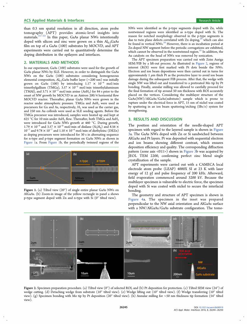
2. MATERIALS AND METHODSIn our experiment, GaAs (100) substrates were used for the growth ofGaAs planar NWs by SLE. However, in order to distinguish the GaAsNWs on the GaAs (100) substrates considering homogeneouselemental composition, Al0.3GaAs buffer layer (∼200 nm) was initiallygrown on GaAs (100) by introducing 1.17 × 10⁻⁴ mol/mintrimethylgallium (TMGa), 3.57 × 10⁻⁵ mol/min trimethylaluminum(TMAl), and 3.71 × 10⁻³ mol/min arsine (AsH3) for 84 s prior to theonset of NW growth by MOCVD in an Aixtron 200/4 horizontal flowMOCVD reactor. Thereafter, planar GaAs NWs were grown in thereactor under atmospheric pressure. TMGa and AsH3 were used asprecursors for Ga and As, respectively, H2 was used as the carrier gas,and 250 nm Au colloids were used as SLE seeding agents. Before theTMGa precursor was introduced, samples were heated up and kept at625 °C for 10 min under AsH3 flow. Thereafter, both TMGa and AsH3were introduced for GaAs NWs growth at 460 °C. During growth,1.79 × 10−6 and 3.57 × 10⁻⁶ mol/min of disilane (Si2H6) and 8.56 ×10⁻⁷ and 9.78 × 10⁻⁷ and 1.10 × 10⁻⁶ mol/min of diethylzinc (DEZn)as doping precursors were introduced for 30 s in alternating sequencefor n-type and p-type segment formation on GaAs NWs as shown inFigure 1a. From Figure 1b, the periodically twinned regions of the
NWs were identified as the p-type segments doped with Zn, whilenontwinned regions were identified as n-type doped with Si. Thereason for notched morphology observed in the p-type segments isdue to twin plane defects correlated with Zn doping,24 which can alsobe found in vertical NWs.34 However, there is an incubation period atZn-doped NW segment before the periodic corrugations are exhibited,which cannot be observed in the nontwinned region.35 In addition, theAu catalysts on the head of NWs was removed by sonication.
The APT specimen preparation was carried out with Zeiss AurigaSEM/FIB by a lift-out process. As illustrated in Figure 2, regions ofinterest (ROI) were first marked with Pt dots beside the NWs.Electron and ion beam depositions were then carried out in turns forapproximately 1 μm thick Pt as the protective layer to avoid ion beamdamage during the subsequent FIB process. After that, the wedge withsingle NW was lifted out and transferred to a pretreated Mo tip by Ptbonding. Finally, annular milling was allowed to carefully proceed forthe final formation of tip around 50 nm thickness with ROI accuratelyplaced on the vertices. Considering the multilayer structure of theGaAs(NW)/AlGaAs/GaAs(substrate) sample which is prone torupture under the electrical force in APT, 15 nm of nickel was coatedby sputtering in an ion beam sputtering/etching (IBs/e) system forstrengthening.
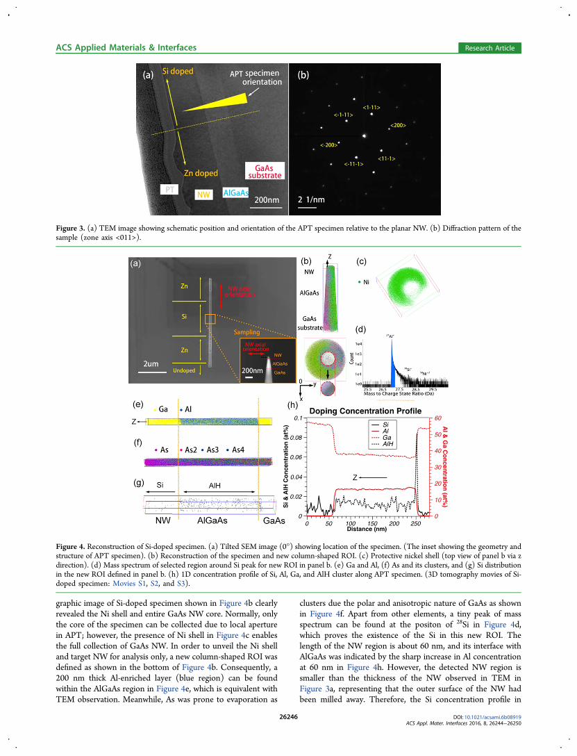
3. RESULTS AND DISCUSSIONThe position and orientation of the needle-shaped APTspecimen with regard to the layered sample is shown in Figure3a. The GaAs NWs doped with Zn or Si sandwiched betweenAlGaAs and Pt layers. Pt was deposited with sequential electronand ion beams showing different contrast, which ensuresdeposition efficiency and quality. The corresponding diffractionpattern (zone axis <011>) shown in Figure 3b was acquired byJEOL TEM 2200, confirming perfect zinc blend singlecrystallization of the sample.APT experiments were carried out with a CAMECA local
electrode atom probe (LEAP) 4000X SI at 23 K with laserenergy of 12 pJ and pulse frequency of 200 kHz. Afterward,field evaporation commenced around 3200 kV. Because themultilayer specimen is vulnerable to electric force, the specimendoped with Si was coated with nickel to secure the interfacialbonding.The geometry and structure of APT specimen is shown in
Figure 4a. The specimen in the inset was preparedperpendicular to the NW axial orientation and AlGaAs surfacewith a NW/AlGaAs/GaAs substrate configuration. The tomo-
Figure 1. (a) Tilted view (20°) of single entire planar GaAs NWs onAlGaAs. (b) Zoom-in image of the yellow rectangle in panel a showsp-type segment doped with Zn and n-type with Si (0° tilted view).
Figure 2. Specimen preparation procedure. (a) Tilted view (0°) of selected ROI, and (b) Pt deposition for protection. (c) Tilted SEM view (24°) ofwedge cutting. (d) Detaching wedge from substrate (10° tilted view). (e) Wedge lifting out (10° tilted view). (f) Wedge transferring (10° tiltedview). (g) Specimen bonding with Mo tip by Pt deposition (20° tilted view). (h) Annular milling for ∼50 nm thickness tip formation (54° tiltedview).
ACS Applied Materials & Interfaces Research Article
DOI: 10.1021/acsami.6b08919ACS Appl. Mater. Interfaces 2016, 8, 26244−26250
26245
graphic image of Si-doped specimen shown in Figure 4b clearlyrevealed the Ni shell and entire GaAs NW core. Normally, onlythe core of the specimen can be collected due to local aperturein APT; however, the presence of Ni shell in Figure 4c enablesthe full collection of GaAs NW. In order to unveil the Ni shelland target NW for analysis only, a new column-shaped ROI wasdefined as shown in the bottom of Figure 4b. Consequently, a200 nm thick Al-enriched layer (blue region) can be foundwithin the AlGaAs region in Figure 4e, which is equivalent withTEM observation. Meanwhile, As was prone to evaporation as
clusters due the polar and anisotropic nature of GaAs as shownin Figure 4f. Apart from other elements, a tiny peak of massspectrum can be found at the positon of 28Si in Figure 4d,which proves the existence of the Si in this new ROI. Thelength of the NW region is about 60 nm, and its interface withAlGaAs was indicated by the sharp increase in Al concentrationat 60 nm in Figure 4h. However, the detected NW region issmaller than the thickness of the NW observed in TEM inFigure 3a, representing that the outer surface of the NW hadbeen milled away. Therefore, the Si concentration profile in
Figure 3. (a) TEM image showing schematic position and orientation of the APT specimen relative to the planar NW. (b) Diffraction pattern of thesample (zone axis <011>).
Figure 4. Reconstruction of Si-doped specimen. (a) Tilted SEM image (0°) showing location of the specimen. (The inset showing the geometry andstructure of APT specimen). (b) Reconstruction of the specimen and new column-shaped ROI. (c) Protective nickel shell (top view of panel b via zdirection). (d) Mass spectrum of selected region around Si peak for new ROI in panel b. (e) Ga and Al, (f) As and its clusters, and (g) Si distributionin the new ROI defined in panel b. (h) 1D concentration profile of Si, Al, Ga, and AlH cluster along APT specimen. (3D tomography movies of Si-doped specimen: Movies S1, S2, and S3).
ACS Applied Materials & Interfaces Research Article
DOI: 10.1021/acsami.6b08919ACS Appl. Mater. Interfaces 2016, 8, 26244−26250
26246
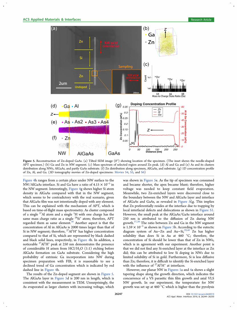
Figure 4h ranges from a certain place under NW surface to theNW/AlGaAs interface. Si and Ga have a ratio of 4.15 × 10⁻⁵ inthe NW segment. Interestingly, Figure 4g shows higher Si atomdensity in AlGaAs compared with that in the NW segment,which seems to be contradictory with the real scenario, giventhat AlGaAs film was not intentionally doped with any element.This can be explained with the mechanism of APT, which isbased on time-of-flight mass spectrometry. As cluster composedof a single 27Al atom and a single 1H with one charge has thesame mass charge ratio as a single 28Si+ atom; therefore, APTregarded them as same element.36 Another aspect is that theconcentration of Al in AlGaAs is 2000 times larger than that ofSi in NW segment; therefore, 27Al1H+ has higher concentrationcompared to that of Si, which are represented by black dashedand black solid lines, respectively, in Figure 4h. In addition, anoticeable 27Al1H+ peak at 250 nm demonstrates the presenceof considerable H arisen from HCl/H2O (1:1) etching beforeAlGaAs formation on GaAs substrate. Considering the highprobability of extrinsic Ga incorporation into NW duringspecimen preparation with FIB, it is reasonable to see adeclined trend of Ga concentration which is indicated by reddashed line in Figure 4h.The results of the Zn-doped segment are shown in Figure 5.
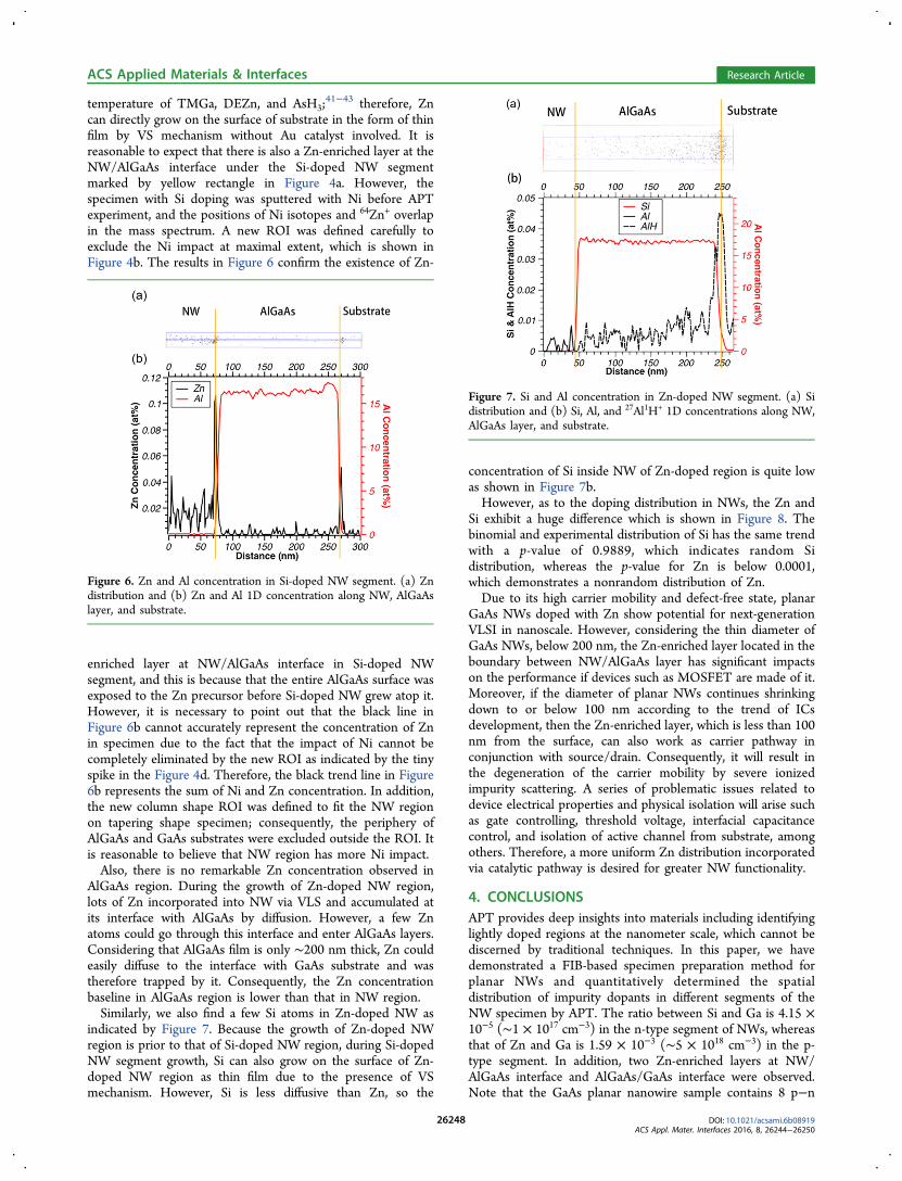
The AlGaAs layer in Figure 5d is 200 nm in length, which isconsistent with the measurement in TEM. Unsurprisingly, theAs evaporated as larger clusters with increasing voltage, which
was shown in Figure 5e. As the tip of specimen was consumedand became shorter, the apex became blunt; therefore, highervoltage was needed to keep constant field evaporation.Meanwhile, two Zn-enriched layers were discovered close tothe boundary between the NW and AlGaAs layer and interfaceof AlGaAs and GaAs, as revealed in Figure 5f,g. This impliesthat Zn preferentially resides at the interface due to trapping bylocal interfacial defects and dislocations as shown in Figure S1.However, the small peak at the AlGaAs/GaAs interface around250 nm is attributed to the diffusion of Zn during NWgrowth.37,38 The ratio between Zn and Ga in the NW segmentis 1.59 × 10⁻³ as shown in Figure 5b. According to the eutecticdiagram system of Au−Zn and Au−Si,39,40 Zn has highersolubility than does Si in Au at 460 °C; therefore, theconcentration of Si should be lower than that of Zn in NWs,which is in agreement with our experiment. Another point isthat we did not find any Si-enriched layer at the interface as Zndid; this can be attributed to low Si doping in NWs due tolimited solubility of Si in gold. Furthermore, Si is less diffusivethan Zn; therefore, it is difficult to identify the Si-enriched layerwith the influence of 27Al1H+ at interfaces.However, our planar NW in Figures 1a and 4a shows a slight
tapering shape along the growth direction, which indicates theconcurrence of a VS parasitic thin film growth and axial VLSNW growth. In our experiment, the temperature for NWgrowth was set up at 460 °C which is higher than the pyrolysis
Figure 5. Reconstruction of Zn-doped GaAs. (a) Tilted SEM image (0°) showing location of the specimen. (The inset shows the needle-shapedAPT specimen.) (b) Ga and Zn in NW segment. (c) Mass spectrum of selected region around Zn peak. (d) Al and Ga and (e) As and its clustersdistribution along NWs, AlGaAs, and partly GaAs substrate. (f) Zn distribution along specimen, AlGaAs, and substrate. (g) 1D concentration profileof Zn, Al, and Ga. (3D tomography movies of Zn-doped specimens: Movies S4, S5, and S6)
ACS Applied Materials & Interfaces Research Article
DOI: 10.1021/acsami.6b08919ACS Appl. Mater. Interfaces 2016, 8, 26244−26250
26247
temperature of TMGa, DEZn, and AsH3;41−43 therefore, Zn
can directly grow on the surface of substrate in the form of thinfilm by VS mechanism without Au catalyst involved. It isreasonable to expect that there is also a Zn-enriched layer at theNW/AlGaAs interface under the Si-doped NW segmentmarked by yellow rectangle in Figure 4a. However, thespecimen with Si doping was sputtered with Ni before APTexperiment, and the positions of Ni isotopes and 64Zn+ overlapin the mass spectrum. A new ROI was defined carefully toexclude the Ni impact at maximal extent, which is shown inFigure 4b. The results in Figure 6 confirm the existence of Zn-
enriched layer at NW/AlGaAs interface in Si-doped NWsegment, and this is because that the entire AlGaAs surface wasexposed to the Zn precursor before Si-doped NW grew atop it.However, it is necessary to point out that the black line inFigure 6b cannot accurately represent the concentration of Znin specimen due to the fact that the impact of Ni cannot becompletely eliminated by the new ROI as indicated by the tinyspike in the Figure 4d. Therefore, the black trend line in Figure6b represents the sum of Ni and Zn concentration. In addition,the new column shape ROI was defined to fit the NW regionon tapering shape specimen; consequently, the periphery ofAlGaAs and GaAs substrates were excluded outside the ROI. Itis reasonable to believe that NW region has more Ni impact.Also, there is no remarkable Zn concentration observed in
AlGaAs region. During the growth of Zn-doped NW region,lots of Zn incorporated into NW via VLS and accumulated atits interface with AlGaAs by diffusion. However, a few Znatoms could go through this interface and enter AlGaAs layers.Considering that AlGaAs film is only ∼200 nm thick, Zn couldeasily diffuse to the interface with GaAs substrate and wastherefore trapped by it. Consequently, the Zn concentrationbaseline in AlGaAs region is lower than that in NW region.Similarly, we also find a few Si atoms in Zn-doped NW as
indicated by Figure 7. Because the growth of Zn-doped NWregion is prior to that of Si-doped NW region, during Si-dopedNW segment growth, Si can also grow on the surface of Zn-doped NW region as thin film due to the presence of VSmechanism. However, Si is less diffusive than Zn, so the
concentration of Si inside NW of Zn-doped region is quite lowas shown in Figure 7b.However, as to the doping distribution in NWs, the Zn and
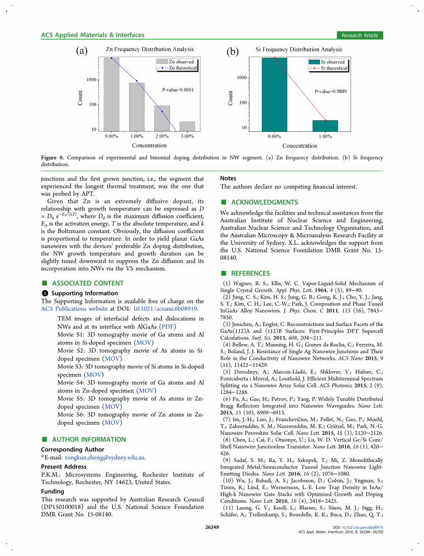
Si exhibit a huge difference which is shown in Figure 8. Thebinomial and experimental distribution of Si has the same trendwith a p-value of 0.9889, which indicates random Sidistribution, whereas the p-value for Zn is below 0.0001,which demonstrates a nonrandom distribution of Zn.Due to its high carrier mobility and defect-free state, planar
GaAs NWs doped with Zn show potential for next-generationVLSI in nanoscale. However, considering the thin diameter ofGaAs NWs, below 200 nm, the Zn-enriched layer located in theboundary between NW/AlGaAs layer has significant impactson the performance if devices such as MOSFET are made of it.Moreover, if the diameter of planar NWs continues shrinkingdown to or below 100 nm according to the trend of ICsdevelopment, then the Zn-enriched layer, which is less than 100nm from the surface, can also work as carrier pathway inconjunction with source/drain. Consequently, it will result inthe degeneration of the carrier mobility by severe ionizedimpurity scattering. A series of problematic issues related todevice electrical properties and physical isolation will arise suchas gate controlling, threshold voltage, interfacial capacitancecontrol, and isolation of active channel from substrate, amongothers. Therefore, a more uniform Zn distribution incorporatedvia catalytic pathway is desired for greater NW functionality.
4. CONCLUSIONSAPT provides deep insights into materials including identifyinglightly doped regions at the nanometer scale, which cannot bediscerned by traditional techniques. In this paper, we havedemonstrated a FIB-based specimen preparation method forplanar NWs and quantitatively determined the spatialdistribution of impurity dopants in different segments of theNW specimen by APT. The ratio between Si and Ga is 4.15 ×10⁻⁵ (∼1 × 1017 cm−3) in the n-type segment of NWs, whereasthat of Zn and Ga is 1.59 × 10⁻³ (∼5 × 1018 cm−3) in the p-type segment. In addition, two Zn-enriched layers at NW/AlGaAs interface and AlGaAs/GaAs interface were observed.Note that the GaAs planar nanowire sample contains 8 p−n
Figure 6. Zn and Al concentration in Si-doped NW segment. (a) Zndistribution and (b) Zn and Al 1D concentration along NW, AlGaAslayer, and substrate.
Figure 7. Si and Al concentration in Zn-doped NW segment. (a) Sidistribution and (b) Si, Al, and 27Al1H+ 1D concentrations along NW,AlGaAs layer, and substrate.
ACS Applied Materials & Interfaces Research Article
DOI: 10.1021/acsami.6b08919ACS Appl. Mater. Interfaces 2016, 8, 26244−26250
26248
junctions and the first grown junction, i.e., the segment thatexperienced the longest thermal treatment, was the one thatwas probed by APT.Given that Zn is an extremely diffusive dopant, its
relationship with growth temperature can be expressed as D= D0 e
−EA/(kT), where D0 is the maximum diffusion coefficient,EA is the activation energy, T is the absolute temperature, and kis the Boltzmann constant. Obviously, the diffusion coefficientis proportional to temperature. In order to yield planar GaAsnanowires with the devices’ preferable Zn doping distribution,the NW growth temperature and growth duration can beslightly tuned downward to suppress the Zn diffusion and itsincorporation into NWs via the VS mechanism.
■ ASSOCIATED CONTENT*S Supporting InformationThe Supporting Information is available free of charge on theACS Publications website at DOI: 10.1021/acsami.6b08919.
TEM images of interfacial defects and dislocations inNWs and at its interface with AlGaAs (PDF)Movie S1: 3D tomography movie of Ga atoms and Alatoms in Si-doped specimen (MOV)Movie S2: 3D tomography movie of As atoms in Si-doped specimen (MOV)Movie S3: 3D tomography movie of Si atoms in Si-dopedspecimen (MOV)Movie S4: 3D tomography movie of Ga atoms and Alatoms in Zn-doped specimen (MOV)Movie S5: 3D tomography movie of As atoms in Zn-doped specimen (MOV)Movie S6: 3D tomography movie of Zn atoms in Zn-doped specimen (MOV)
■ AUTHOR INFORMATIONCorresponding Author*E-mail: [email protected] AddressP.K.M.: Microsystems Engineering, Rochester Institute ofTechnology, Rochester, NY 14623, United States.FundingThis research was supported by Australian Research Council(DP150100018) and the U.S. National Science FoundationDMR Grant No. 15-08140.
NotesThe authors declare no competing financial interest.
■ ACKNOWLEDGMENTS
We acknowledge the facilities and technical assistances from theAustralian Institute of Nuclear Science and Engineering,Australian Nuclear Science and Technology Organisation, andthe Australian Microscopy & Microanalysis Research Facility atthe University of Sydney. X.L. acknowledges the support fromthe U.S. National Science Foundation DMR Grant No. 15-08140.
■ REFERENCES(1) Wagner, R. S.; Ellis, W. C. Vapor-Liquid-Solid Mechanism ofSingle Crystal Growth. Appl. Phys. Lett. 1964, 4 (5), 89−90.(2) Jung, C. S.; Kim, H. S.; Jung, G. B.; Gong, K. J.; Cho, Y. J.; Jang,S. Y.; Kim, C. H.; Lee, C.-W.; Park, J. Composition and Phase TunedInGaAs Alloy Nanowires. J. Phys. Chem. C 2011, 115 (16), 7843−7850.(3) Jenichen, A.; Engler, C. Reconstructions and Surface Facets of theGaAs(112)A and (112)B Surfaces: First-Principles DFT SupercellCalculations. Surf. Sci. 2013, 608, 204−211.(4) Bellew, A. T.; Manning, H. G.; Gomes da Rocha, C.; Ferreira, M.S.; Boland, J. J. Resistance of Single Ag Nanowire Junctions and TheirRole in the Conductivity of Nanowire Networks. ACS Nano 2015, 9(11), 11422−11429.(5) Dorodnyy, A.; Alarcon-Llado, E.; Shklover, V.; Hafner, C.;Fontcuberta i Morral, A.; Leuthold, J. Efficient Multiterminal SpectrumSplitting via a Nanowire Array Solar Cell. ACS Photonics 2015, 2 (9),1284−1288.(6) Fu, A.; Gao, H.; Petrov, P.; Yang, P. Widely Tunable DistributedBragg Reflectors Integrated into Nanowire Waveguides. Nano Lett.2015, 15 (10), 6909−6913.(7) Im, J.-H.; Luo, J.; Franckevicius, M.; Pellet, N.; Gao, P.; Moehl,T.; Zakeeruddin, S. M.; Nazeeruddin, M. K.; Gratzel, M.; Park, N.-G.Nanowire Perovskite Solar Cell. Nano Lett. 2015, 15 (3), 2120−2126.(8) Chen, L.; Cai, F.; Otuonye, U.; Lu, W. D. Vertical Ge/Si Core/Shell Nanowire Junctionless Transistor. Nano Lett. 2016, 16 (1), 420−426.(9) Sadaf, S. M.; Ra, Y. H.; Szkopek, T.; Mi, Z. MonolithicallyIntegrated Metal/Semiconductor Tunnel Junction Nanowire Light-Emitting Diodes. Nano Lett. 2016, 16 (2), 1076−1080.(10) Wu, J.; Babadi, A. S.; Jacobsson, D.; Colvin, J.; Yngman, S.;Timm, R.; Lind, E.; Wernersson, L.-E. Low Trap Density in InAs/High-k Nanowire Gate Stacks with Optimized Growth and DopingConditions. Nano Lett. 2016, 16 (4), 2418−2425.(11) Luong, G. V.; Knoll, L.; Blaeser, S.; Suess, M. J.; Sigg, H.;Schafer, A.; Trellenkamp, S.; Bourdelle, K. K.; Buca, D.; Zhao, Q. T.;
Figure 8. Comparison of experimental and binomial doping distribution in NW segment. (a) Zn frequency distribution. (b) Si frequencydistribution.
ACS Applied Materials & Interfaces Research Article
DOI: 10.1021/acsami.6b08919ACS Appl. Mater. Interfaces 2016, 8, 26244−26250
26249
Mantl, S. Demonstration of Higher Electron Mobility in Si NanowireMOSFETs by Increasing the Strain Beyond 1.3%. Solid-State Electron.2015, 108, 19−23.(12) Gradecak, S.; Qian, F.; Li, Y.; Park, H.-G.; Lieber, C. M. GaNNanowire Lasers with Low Lasing Thresholds. Appl. Phys. Lett. 2005,87 (17), 173111−173113.(13) Mohseni, P. K.; Behnam, A.; Wood, J. D.; Zhao, X.; Yu, K. J.;Wang, N. C.; Rockett, A.; Rogers, J. A.; Lyding, J. W.; Pop, E.; Li, X.Monolithic III-V Nanowire Solar Cells on Graphene via Direct VanDer Waals Epitaxy. Adv. Mater. 2014, 26 (22), 3755−3760.(14) Mallorquí, A. D.; Alarco n-Llado , E.; Russo-Averchi, E.;Tutuncuoglu, G.; Matteini, F.; Ruffer, D.; Morral, A. F. i. Character-ization and Analysis of InAs/p−Si Heterojunction Nanowire-BasedSolar Cell. J. Phys. D: Appl. Phys. 2014, 47 (39), 394017−394025.(15) Dowdy, R.; Walko, D. A.; Fortuna, S. A.; Li, X. Realization ofUnidirectional Planar GaAs Nanowires on GaAs (110) Substrates.IEEE Electron Device Lett. 2012, 33 (4), 522−524.(16) Dowdy, R. S.; Walko, D. A.; Li, X. Relationship Between PlanarGaAs Nanowire Growth Direction and Substrate Orientation.Nanotechnology 2013, 24 (3), 035304−035310.(17) Shen, Y.; Turner, S.; Yang, P.; Van Tendeloo, G.; Lebedev, O. I.;Wu, T. Epitaxy-Enabled Vapor−Liquid−Solid Growth of Tin-DopedIndium Oxide Nanowires with Controlled Orientations. Nano Lett.2014, 14 (8), 4342−4351.(18) Nikoobakht, B. Toward Industrial-Scale Fabrication of Nano-wire-Based Devices. Chem. Mater. 2007, 19 (22), 5279−5284.(19) Zi, Y.; Jung, K.; Zakharov, D.; Yang, C. Understanding Self-Aligned Planar Growth of InAs Nanowires. Nano Lett. 2013, 13 (6),2786−2791.(20) Zhang, C.; Miao, X.; Mohseni, P. K.; Choi, W.; Li, X. Site-Controlled VLS Growth of Planar Nanowires: Yield and Mechanism.Nano Lett. 2014, 14 (12), 6836−6841.(21) Miao, X.; Chabak, K.; Zhang, C.; Katal Mohseni, P.; Walker, D.,Jr.; Li, X. High-Speed Planar GaAs Nanowire Arrays with f > 75 GHzby Wafer-Scale Bottom-up Growth. Nano Lett. 2015, 15 (5), 2780−2786.(22) Zhang, C.; Li, X. Planar GaAs Nanowire Tri-Gate MOSFETs byVapor−Liquid−Solid Growth. Solid-State Electron. 2014, 93, 40−42.(23) Fortuna, S. A.; Wen, J.; Chun, I. S.; Li, X. Planar GaAsNanowires on GaAs (100) Substrates: Self-Aligned, Nearly Twin-Defect Free, and Transfer-Printable. Nano Lett. 2008, 8 (12), 4421−4427.(24) Miao, X.; Zhang, C.; Li, X. Monolithic Barrier-All-Around HighElectron Mobility Transistor with Planar GaAs Nanowire Channel.Nano Lett. 2013, 13 (6), 2548−2552.(25) Putnam, M. C.; Filler, M. A.; Kayes, B. M.; Kelzenberg, M. D.;Guan, Y.; Lewis, N. S.; Eiler, J. M.; Atwater, H. A. Secondary Ion MassSpectrometry of Vapor−Liquid−Solid Grown, Au-Catalyzed, Si Wires.Nano Lett. 2008, 8 (10), 3109−3113.(26) Bullis, W. M. Properties of Gold in Silicon. Solid-State Electron.1966, 9 (2), 143−168.(27) Wang, X.; Yang, X.; Du, W.; Ji, H.; Luo, S.; Yang, T. ThicknessInfluence of Thermal Oxide Layers on The Formation of Self-Catalyzed InAs Nanowires on Si(111) by MOCVD. J. Cryst. Growth2014, 395, 55−60.(28) Riley, J. R.; Bernal, R. A.; Li, Q.; Espinosa, H. D.; Wang, G. T.;Lauhon, L. J. Atom Probe Tomography of a-Axis GaN Nanowires:Analysis of Nonstoichiometric Evaporation Behavior. ACS Nano 2012,6 (5), 3898−3906.(29) Kasapoglu, E.; Duque, C. A.; Sakirog lu, S.; Sari, H.; Sokmen, I.The Effects of the Intense Laser Field on Donor Impurities in aCylindrical Quantum Dot under the Electric Field. Phys. E 2011, 43(8), 1427−1432.(30) Allen, J. E.; Hemesath, E. R.; Perea, D. E.; Lensch-Falk, J. L.; Li,Z. Y.; Yin, F.; Gass, M. H.; Wang, P.; Bleloch, A. L.; Palmer, R. E.;Lauhon, L. J. High-Resolution Detection of Au Catalyst Atoms in SiNanowires. Nat. Nanotechnol. 2008, 3 (3), 168−173.(31) Kelly, T. F.; Larson, D. J. Atom Probe Tomography 2012. Annu.Rev. Mater. Res. 2012, 42 (1), 1−31.
(32) Cerezo, A.; Clifton, P. H.; Galtrey, M. J.; Humphreys, C. J.;Kelly, T. F.; Larson, D. J.; Lozano-Perez, S.; Marquis, E. A.; Oliver, R.A.; Sha, G.; Thompson, K.; Zandbergen, M.; Alvis, R. L. Atom ProbeTomography Today. Mater. Today 2007, 10 (12), 36−42.(33) Qu, J.; Ringer, S.; Zheng, R. Atomic-Scale Tomography ofSemiconductor Nanowires. Mater. Sci. Semicond. Process. 2015, 40,896−909.(34) Algra, R. E.; Verheijen, M. A.; Borgstrom, M. T.; Feiner, L.-F.;Immink, G.; van Enckevort, W. J. P.; Vlieg, E.; Bakkers, E. P. A. M.Twinning Superlattices in Indium Phosphide Nanowires. Nature 2008,456 (7220), 369−372.(35) Dowdy, R. S.; Zhang, C.; Mohseni, P. K.; Fortuna, S. A.; Wen,J.-G.; Coleman, J. J.; Li, X. Perturbation of Au-assisted planar GaAsnanowire growth by p-type dopant impurities. Opt. Mater. Express2013, 3 (10), 1687−1697.(36) Gault, B.; Moody, M. P.; Cairney, J. M.; Ringer, S. P. Atom ProbeMicroscopy, 2012 ed; Springer-Verlag: New York, New York, 2012.(37) Reichert, W.; Chen, C. Y.; Li, W. M.; Shield, J. E.; Cohen, R. M.;Simons, D. S.; Chi, P. H. Incorporation of Zn in GaAs duringOrganometallic Vapor Phase Epitaxy Growth Compared to Equili-brium. J. Appl. Phys. 1995, 77 (5), 1902−1906.(38) Ky, N. H.; Pavesi, L.; Araujo, D.; Ganiere, J. D.; Reinhart, F. K.A Model for the Zn Diffusion in GaAs by a Photoluminescence Study.J. Appl. Phys. 1991, 69 (11), 7585−7593.(39) Okamoto, H.; Massalski, T. B. The Au-Si(Gold-Silicon) System.Bull. Alloy Phase Diagrams 1983, 4 (2), 190−198.(40) Okamoto, H.; Massalski, T. B. The Au-Zn (Gold-Zinc) System.Bull. Alloy Phase Diagrams 1989, 10 (1), 59−69.(41) Li, S. H.; Larsen, C. A.; Chen, C. H.; Stringfellow, G. B.; Brown,D. W. Dimethylarsine: Pyrolysis Mechanisms and Use for OMVPEGrowth. J. Electron. Mater. 1990, 19 (4), 299−304.(42) Francis, J. T.; Benson, S. W.; Tsotsis, T. T. Kinetics of the VeryLow Pressure Pyrolysis of Trimethylgallium and Arsine. J. Cryst.Growth 1991, 112 (2), 474−486.(43) Thiandoume, C.; Sallet, V.; Triboulet, R.; Gorochov, O.Decomposition Kinetics of Tertiarybutanol and Diethylzinc Used asPrecursor Sources for the Growth of ZnO. J. Cryst. Growth 2009, 311(5), 1411−1415.
ACS Applied Materials & Interfaces Research Article
DOI: 10.1021/acsami.6b08919ACS Appl. Mater. Interfaces 2016, 8, 26244−26250
26250