Embed Size (px)
Citation preview
DME SWITCHER
DFS-700ADFS-700APDFS-700DFS-700P
SERVICE MANUAL
Volume 1 1st Edition (Revised 2)
DIGITAL/ANALOG INPUT BOARD
ANALOG COMPOSITE INPUT BOARD
BKDF-702/702P
BKDF-701
DIGITAL MULTI EFFECTS BOARD
BKDF-711
BKDF-7123D VIDEO MAPPING EFFECTS BOARD
DFS-700A/700AP/700/700P
! WARNINGThis manual is intended for qualified service personnel only.To reduce the risk of electric shock, fire or injury, do not perform any servicing other than thatcontained in the operating instructions unless you are qualified to do so. Refer all servicing toqualified service personnel.
! WARNUNGDie Anleitung ist nur für qualifiziertes Fachpersonal bestimmt.Alle Wartungsarbeiten dürfen nur von qualifiziertem Fachpersonal ausgeführt werden. Um dieGefahr eines elektrischen Schlages, Feuergefahr und Verletzungen zu vermeiden, sind beiWartungsarbeiten strikt die Angaben in der Anleitung zu befolgen. Andere als die angegebenWartungsarbeiten dürfen nur von Personen ausgeführt werden, die eine spezielle Befähigungdazu besitzen.
! AVERTISSEMENTCe manual est destiné uniquement aux personnes compétentes en charge de l’entretien. Afinde réduire les risques de décharge électrique, d’incendie ou de blessure n’effectuer que lesréparations indiquées dans le mode d’emploi à moins d’être qualifié pour en effectuer d’autres.Pour toute réparation faire appel à une personne compétente uniquement.
1DFS-700A/700AP/700/700P
Table of Contents
Manual Structure
Purpose of this manual .............................................................................................. 5
Related manuals ......................................................................................................... 5
Contents ..................................................................................................................... 6
1. Operating Instructions
Please refer to the instruction manual.
2. Service Overview
2-1. Installation ................................................................................................... 2-12-1-1. Operating Environment .............................................................. 2-12-1-2. Power Supply Specifications ...................................................... 2-12-1-3. Power Supply Cord .................................................................... 2-12-1-4. Installation Space ....................................................................... 2-22-1-5. Matching Connector and Cable .................................................. 2-32-1-6. Signal Input/Output .................................................................... 2-42-1-7. Rack Mounting ........................................................................... 2-72-1-8. Installing Optional Board ........................................................... 2-9
2-2. Removal of Cabinet ................................................................................... 2-10
2-3. Location of Main Parts .............................................................................. 2-11
2-4. Circuit Description .................................................................................... 2-122-4-1. Processor .................................................................................. 2-122-4-2. Control Panel ............................................................................ 2-19
2-5. Replacement of Board ............................................................................... 2-212-5-1. Replacement of Plug-in Board ................................................. 2-212-5-2. Replacement of Board .............................................................. 2-21
2-6. Replacement of Switching Regulator ........................................................ 2-23
2-7. Replacement of DC Fan ............................................................................ 2-24
2-8. Replacement of Main Parts on Control Panel ........................................... 2-252-8-1. Replacement of Fader Assembly ............................................. 2-252-8-2. Replacement of Rotary Encoder .............................................. 2-262-8-3. Replacement of Joystick .......................................................... 2-262-8-4. Replacement of Vacuum Fluorescent Display ......................... 2-27
2-9. Fuse/IC Link Replacement ........................................................................ 2-28
2-10. Switch, Indicators, and Volume Controls on Board ................................. 2-292-10-1. Control Panel ............................................................................ 2-292-10-2. Processor .................................................................................. 2-30
2-11. Error Indication ......................................................................................... 2-43
2-12. Periodic Inspection .................................................................................... 2-442-12-1. Periodic Replacement Parts ...................................................... 2-442-12-2. Filter Cleaning .......................................................................... 2-44
2 DFS-700A/700AP/700/700P
2-13. Fixtures/Measuring Instruments ................................................................ 2-442-13-1. Fixtures ..................................................................................... 2-442-13-2. How to Use Extension Board ................................................... 2-452-13-3. Measuring Instruments ............................................................. 2-45
3. Self-diagnosis
3-1. Confirmation of Version ............................................................................. 3-23-1-1. Execution .................................................................................... 3-23-1-2. Viewing the Version .................................................................. 3-3
3-2. Check Mode ................................................................................................ 3-33-2-1. Activation and Termination ....................................................... 3-33-2-2. Basic Operation .......................................................................... 3-43-2-3. Checking .................................................................................... 3-5
3-3. Troubleshooting .......................................................................................... 3-9
4. Electrical Alignment
4-1. Adjustment Sequence .................................................................................. 4-1
4-2. Preparation for Adjustment ......................................................................... 4-5
4-3. OPM-39/OPM-45 Board Adjustment (For NTSC) ..................................... 4-64-3-1. +5 V DC Voltage Adjustment ................................................... 4-64-3-2. +3.3 V DC Voltage Adjustment ................................................ 4-64-3-3. SDI VCO Free-running Frequency Adjustment ........................ 4-64-3-4. PGM OUT Component Y Gain Adjustment .............................. 4-74-3-5. PGM OUT Component R-Y Gain Adjustment .......................... 4-74-3-6. PGM OUT Component B-Y Gain Adjustment .......................... 4-84-3-7. PGM OUT Component Y/C Delay Adjustment ........................ 4-84-3-8. Composite SC Leak Balance Adjustment .................................. 4-94-3-9. Composite Y Gain Adjustment .................................................. 4-94-3-10. Composite Modulation AXIS Adjustment ............................... 4-104-3-11. Composite Y/C Delay Adjustment ........................................... 4-114-3-12. Composite C Gain Adjustment ................................................ 4-114-3-13. Composite Burst Level Adjustment ......................................... 4-124-3-14. S VIDEO Y Gain Adjustment .................................................. 4-124-3-15. S VIDEO C Gain Adjustment .................................................. 4-134-3-16. Black Burst OUT SC Leak Balance Adjustment ..................... 4-134-3-17. Black Burst OUT SC Phase Adjustment .................................. 4-144-3-18. Black Burst OUT SYNC Level Adjustment ............................ 4-144-3-19. Black Burst OUT Burst Level Adjustment .............................. 4-154-3-20. INT SC Frequency Adjustment ................................................ 4-154-3-21. INT SCH Phase Adjustment .................................................... 4-164-3-22. INT Black Burst OUT SCH Phase Adjustment ....................... 4-174-3-23. GEN Lock H Phase Adjustment .............................................. 4-184-3-24. GEN Lock SC Phase Adjustment ............................................ 4-19
3DFS-700A/700AP/700/700P
4-3-25. PVW OUT Video Gain Adjustment ........................................ 4-204-3-26. DSK EXT Key Clamp Level Adjustment ................................ 4-204-3-27. DSK EXT Key Gain Adjustment ............................................. 4-21
4-4. OPM-39P/OPM-45P Board Adjustment (For PAL) ................................. 4-224-4-1. +5 V DC Voltage Adjustment ................................................. 4-224-4-2. +3.3 V DC Voltage Adjustment .............................................. 4-224-4-3. SDI VCO Free-running Frequency Adjustment ...................... 4-224-4-4. PGM OUT Component Y Gain Adjustment ............................ 4-234-4-5. PGM OUT Component R-Y Gain Adjustment ........................ 4-234-4-6. PGM OUT Component B-Y Gain Adjustment ........................ 4-244-4-7. PGM OUT Component Y/C Delay Adjustment ...................... 4-244-4-8. Composite SC Leak Balance Adjustment ................................ 4-254-4-9. Composite Y Gain Adjustment ................................................ 4-254-4-10. Composite Modulation AXIS Adjustment ............................... 4-264-4-11. Composite Y/C Delay Adjustment ........................................... 4-274-4-12. Composite C Gain Adjustment ................................................ 4-274-4-13. Composite Burst Balance Adjustment ..................................... 4-284-4-14. Composite Burst Level Adjustment ......................................... 4-284-4-15. S VIDEO Y Gain Adjustment .................................................. 4-294-4-16. S VIDEO C Gain Adjustment .................................................. 4-294-4-17. Black Burst OUT SC Leak Balance Adjustment ..................... 4-304-4-18. Black Burst OUT Burst Balance Adjustment .......................... 4-304-4-19. Black Burst OUT SC Phase Adjustment .................................. 4-314-4-20. Black Burst OUT SYNC Level Adjustment ............................ 4-314-4-21. Black Burst OUT Burst Level Adjustment .............................. 4-324-4-22. INT SC Frequency Adjustment ................................................ 4-324-4-23. INT SCH Phase Adjustment .................................................... 4-334-4-24. INT Black Burst OUT SCH Phase Adjustment ....................... 4-344-4-25. Preread ON PGM OUT SCH Phase Adjustment ..................... 4-354-4-26. Preread ON PGM OUT Burst Start Adjustment ...................... 4-364-4-27. GEN Lock H Phase Adjustment .............................................. 4-374-4-28. GEN Lock SC Phase Adjustment ............................................ 4-384-4-29. PVW OUT Video Gain Adjustment ........................................ 4-394-4-30. DSK EXT Key Clamp Level Adjustment ................................ 4-394-4-31. DSK EXT Key Gain Adjustment ............................................. 4-40
4-5. IPM-96/96P Board Adjustment ................................................................. 4-414-5-1. SDI VCO Free-running Frequency Adjustment ...................... 4-414-5-2. Component Y Level Adjustment ............................................. 4-424-5-3. Component Chroma Level Adjustment ................................... 4-434-5-4. Input Y/C Delay Adjustment ................................................... 4-454-5-5. Video Input Phase Adjustment ................................................. 4-464-5-6. RGB Converted Y Level Adjustment ...................................... 4-474-5-7. RGB Converted Chroma Level Adjustment ............................ 4-48
4 DFS-700A/700AP/700/700P
4-6. VIF-19/19P Board Adjustment ................................................................. 4-504-6-1. Composite Y Level Adjustment ............................................... 4-504-6-2. S VIDEO Clamp DC Level Adjustment .................................. 4-524-6-3. SYNC Separate Adjustment ..................................................... 4-544-6-4. H Lock Loop Adjustment ......................................................... 4-554-6-5. Burst Delay Adjustment ........................................................... 4-574-6-6. Composite Input Y Gain Adjustment ....................................... 4-594-6-7. Composite Input Chroma Level Adjustment ........................... 4-614-6-8. S VIDEO Input Gain Adjustment ............................................ 4-634-6-9. Composite Input Y/C Delay Adjustment ................................. 4-654-6-10. S VIDEO Input Y/C Delay Adjustment ................................... 4-694-6-11. Video Input Phase Adjustment ................................................. 4-73
4-7. VIF-20/20P Board Adjustment ................................................................. 4-744-7-1. SDI VCO Free-running Frequency Adjustment ...................... 4-744-7-2. Component Y Level Adjustment ............................................. 4-754-7-3. Component Chroma Level Adjustment ................................... 4-764-7-4. Input Y/C Delay Adjustment ................................................... 4-784-7-5. Video Input Phase Adjustment ................................................. 4-79
4-8. Adjusting the Power Supply Voltage ........................................................ 4-80
5DFS-700A/700AP/700/700P
Manual Structure
Purpose of this manualThis manual is the service manual Vol.1 of the DME Switcher DFS-700A/700AP/700/700P and their optional boards.The service manuals (Vol.1 and Vol.2) are intended for use by trained system andservice engineers, and describes the information on installing, maintenance, anddetailed service.
This manual (Vol.1) describes the service overviews, diagnosis, and electricalalignment.
Related manualsBesides this Service Manual Vol.1, the following manuals are available for theDFS-700A/700AP/700/700P.
..... Service Manual Vol.2Part No. 9-967-898-XX (for J, UC, CE)Contains the spare parts, semiconductor pin assingments, block diagrams,schematic diagrams, and board layouts.
..... “Semiconductor Pin Assignments” CD-ROM (Available on request)This “Semiconductor Pin Assignments” CD-ROM allows you to search forsemiconductors used in B&P Company equipment.Semiconductors that cannot be searched for on this CD-ROM are listed in theservice manual for the corresponding unit. The service manual contains a com-plete list of all semiconductors and their ID Nos., and thus should be used togetherwith the CD-ROM.Part number: 9-968-546-XX
6 DFS-700A/700AP/700/700P
ContentsThis manual is organized by following sections.
Section 1 Operating InstructionsPlease refer to the operating instructions supplied with this unit.
Section 2 Service OverviewThis section explains the information that is required for installing (the operatingconditions, power supply and power cords, installaion of the optional board, rackmounting, adaptive connectors), outline of the board circuit, replacement of the parts,switch setting on the board, error indication, and tools and adjustment equipment.
Section 3 Self-diagnosisThis section explains the activation (termination) of the check mode in this unit, thebasic operation, and the check method.
Section 4 Electrical AlignmentThis section explains the adjustment of the OPM-39/OPM-45, IPM-69, VIF-19,and VIF-20 boards.
2-1DFS-700A/700AP/700/700P
Section 2Service Overview
2-1. Installation
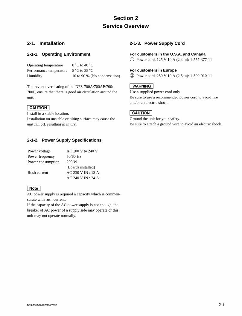
2-1-1. Operating Environment
Operating temperature 0 dC to 40 dCPerformance temperature 5 dC to 35 dCHumidity 10 to 90 % (No condensation)
To prevent overheating of the DFS-700A/700AP/700/700P, ensure that there is good air circulation around theunit.
cInstall in a stable location.Installation on unstable or tilting surface may cause theunit fall off, resulting in injury.
2-1-2. Power Supply Specifications
Power voltage AC 100 V to 240 VPower frequency 50/60 HzPower consumption 200 W
(Boards installed)Rush current AC 230 V IN : 13 A
AC 240 V IN : 24 A
nAC power supply is required a capacity which is commen-surate with rush current.If the capacity of the AC power supply is not enough, thebreaker of AC power of a supply side may operate or thisunit may not operate normally.
2-1-3. Power Supply Cord
For customers in the U.S.A. and Canada1 Power cord, 125 V 10 A (2.4 m): 1-557-377-11
For customers in Europe2 Power cord, 250 V 10 A (2.5 m): 1-590-910-11
wUse a supplied power cord only.Be sure to use a recommended power cord to avoid fireand/or an electric shock.
cGround the unit for your safety.Be sure to attach a ground wire to avoid an electric shock.
2-2 DFS-700A/700AP/700/700P
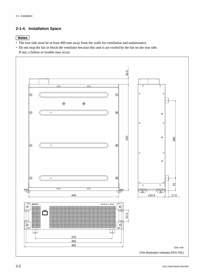
2-1-4. Installation Space
m. The rear side must be at least 400 mm away from the walls for ventilation and maintenance.. Do not stop the fan or block the ventilator because this unit is air-cooled by the fan on the rear side.
If not, a failure or trouble may occur.
26.5
520
440
465
57.2
375
482
6138
0
17.5132.4
2-1. Installation
Unit: mm
(The illustration indicates DFS-700.)
2-3DFS-700A/700AP/700/700P
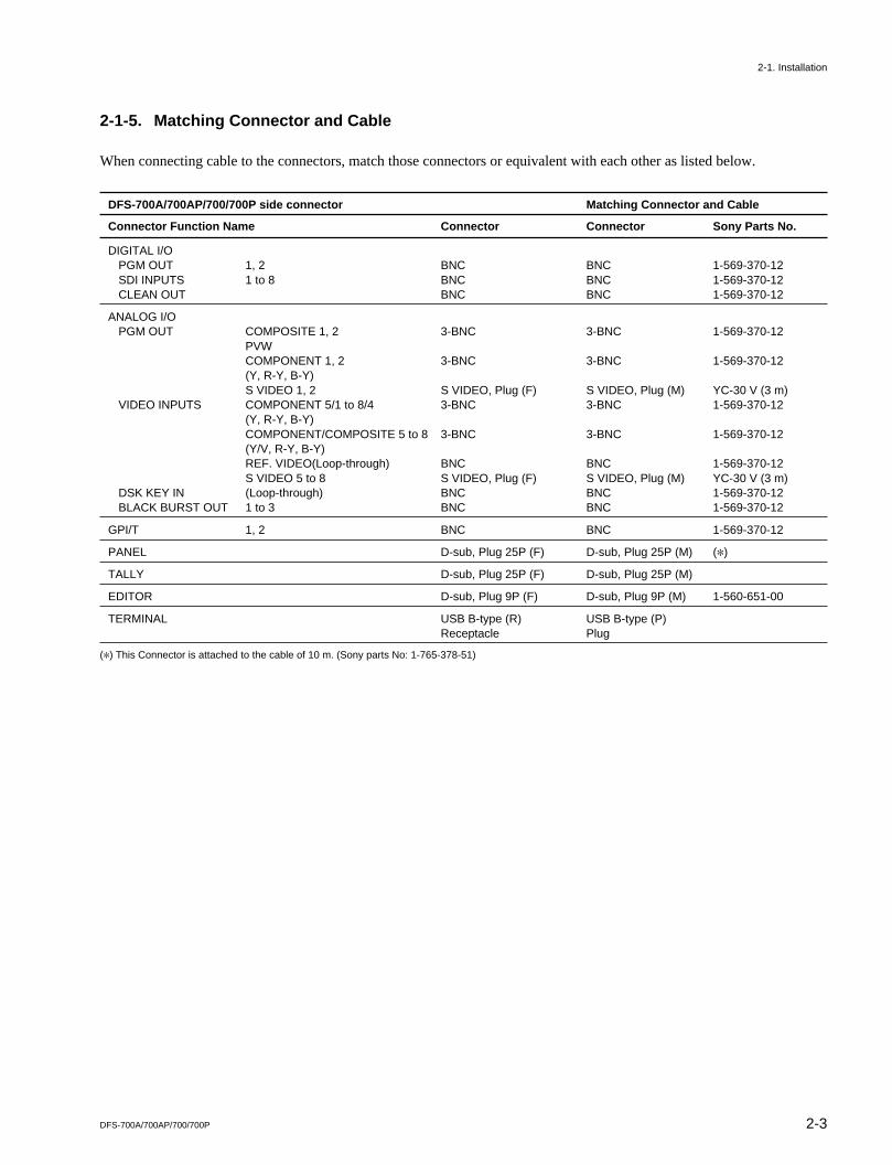
2-1-5. Matching Connector and Cable
When connecting cable to the connectors, match those connectors or equivalent with each other as listed below.
DFS-700A/700AP/700/700P side connector Matching Connector and Cable
Connector Function Name Connector Connector Sony Parts No.
DIGITAL I/OPGM OUT 1, 2 BNC BNC 1-569-370-12SDI INPUTS 1 to 8 BNC BNC 1-569-370-12CLEAN OUT BNC BNC 1-569-370-12
ANALOG I/OPGM OUT COMPOSITE 1, 2 3-BNC 3-BNC 1-569-370-12
PVWCOMPONENT 1, 2 3-BNC 3-BNC 1-569-370-12(Y, R-Y, B-Y)S VIDEO 1, 2 S VIDEO, Plug (F) S VIDEO, Plug (M) YC-30 V (3 m)
VIDEO INPUTS COMPONENT 5/1 to 8/4 3-BNC 3-BNC 1-569-370-12(Y, R-Y, B-Y)COMPONENT/COMPOSITE 5 to 8 3-BNC 3-BNC 1-569-370-12(Y/V, R-Y, B-Y)REF. VIDEO(Loop-through) BNC BNC 1-569-370-12S VIDEO 5 to 8 S VIDEO, Plug (F) S VIDEO, Plug (M) YC-30 V (3 m)
DSK KEY IN (Loop-through) BNC BNC 1-569-370-12BLACK BURST OUT 1 to 3 BNC BNC 1-569-370-12
GPI/T 1, 2 BNC BNC 1-569-370-12
PANEL D-sub, Plug 25P (F) D-sub, Plug 25P (M) (*)
TALLY D-sub, Plug 25P (F) D-sub, Plug 25P (M)
EDITOR D-sub, Plug 9P (F) D-sub, Plug 9P (M) 1-560-651-00
TERMINAL USB B-type (R) USB B-type (P)Receptacle Plug
(*) This Connector is attached to the cable of 10 m. (Sony parts No: 1-765-378-51)
2-1. Installation
2-4 DFS-700A/700AP/700/700P
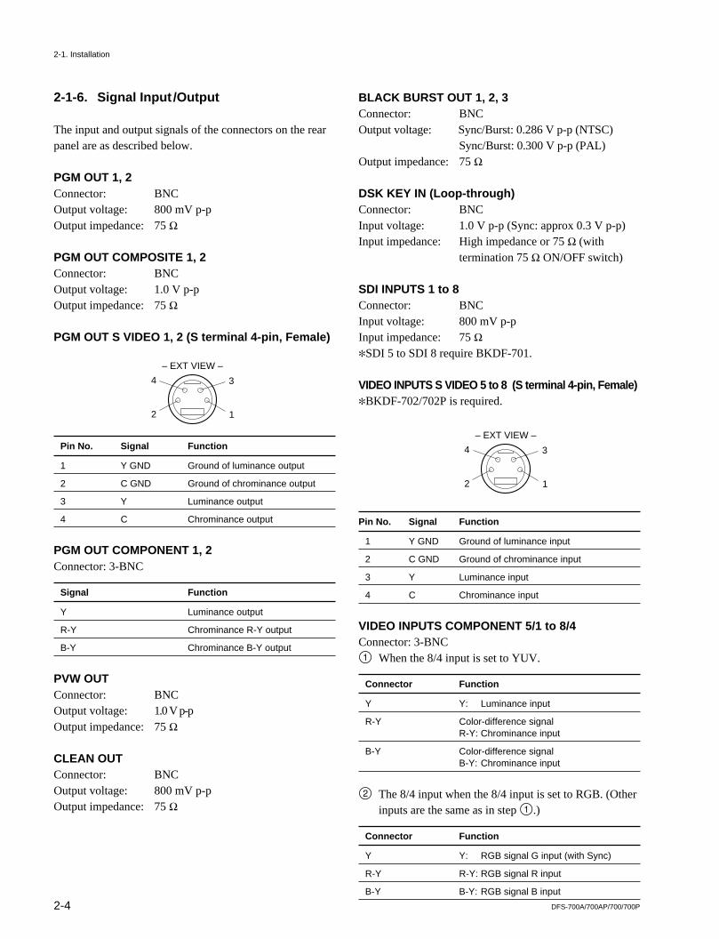
2-1-6. Signal Input /Output
The input and output signals of the connectors on the rearpanel are as described below.
PGM OUT 1, 2Connector: BNCOutput voltage: 800 mV p-pOutput impedance: 75 Z
PGM OUT COMPOSITE 1, 2Connector: BNCOutput voltage: 1.0 V p-pOutput impedance: 75 Z
PGM OUT S VIDEO 1, 2 (S terminal 4-pin, Female)
Pin No. Signal Function
1 Y GND Ground of luminance output
2 C GND Ground of chrominance output
3 Y Luminance output
4 C Chrominance output
PGM OUT COMPONENT 1, 2Connector: 3-BNC
Signal Function
Y Luminance output
R-Y Chrominance R-Y output
B-Y Chrominance B-Y output
PVW OUTConnector: BNCOutput voltage: 1.0 V p-pOutput impedance: 75 Z
CLEAN OUTConnector: BNCOutput voltage: 800 mV p-pOutput impedance: 75 Z
BLACK BURST OUT 1, 2, 3Connector: BNCOutput voltage: Sync/Burst: 0.286 V p-p (NTSC)
Sync/Burst: 0.300 V p-p (PAL)Output impedance: 75 Z
DSK KEY IN (Loop-through)Connector: BNCInput voltage: 1.0 V p-p (Sync: approx 0.3 V p-p)Input impedance: High impedance or 75 Z (with
termination 75 Z ON/OFF switch)
SDI INPUTS 1 to 8Connector: BNCInput voltage: 800 mV p-pInput impedance: 75 Z*SDI 5 to SDI 8 require BKDF-701.
VIDEO INPUTS S VIDEO 5 to 8 (S terminal 4-pin, Female)*BKDF-702/702P is required.
Pin No. Signal Function
1 Y GND Ground of luminance input
2 C GND Ground of chrominance input
3 Y Luminance input
4 C Chrominance input
VIDEO INPUTS COMPONENT 5/1 to 8/4Connector: 3-BNC1 When the 8/4 input is set to YUV.
Connector Function
Y Y: Luminance input
R-Y Color-difference signalR-Y: Chrominance input
B-Y Color-difference signalB-Y: Chrominance input
2 The 8/4 input when the 8/4 input is set to RGB. (Otherinputs are the same as in step 1.)
Connector Function
Y Y: RGB signal G input (with Sync)
R-Y R-Y: RGB signal R input
B-Y B-Y: RGB signal B input
2
4 3
1
– EXT VIEW –
2
4 3
1
– EXT VIEW –
2-1. Installation
2-5DFS-700A/700AP/700/700P
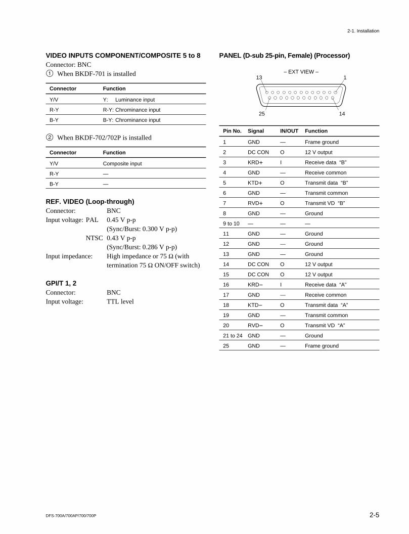
VIDEO INPUTS COMPONENT/COMPOSITE 5 to 8Connector: BNC1 When BKDF-701 is installed
Connector Function
Y/V Y: Luminance input
R-Y R-Y: Chrominance input
B-Y B-Y: Chrominance input
2 When BKDF-702/702P is installed
Connector Function
Y/V Composite input
R-Y —
B-Y —
REF. VIDEO (Loop-through)Connector: BNCInput voltage: PAL 0.45 V p-p
(Sync/Burst: 0.300 V p-p)NTSC 0.43 V p-p
(Sync/Burst: 0.286 V p-p)Input impedance: High impedance or 75 Z (with
termination 75 Z ON/OFF switch)
GPI/T 1, 2Connector: BNCInput voltage: TTL level
PANEL (D-sub 25-pin, Female) (Processor)
Pin No. Signal IN/OUT Function
1 GND — Frame ground
2 DC CON O 12 V output
3 KRD+ I Receive data “B”
4 GND — Receive common
5 KTD+ O Transmit data “B”
6 GND — Transmit common
7 RVD+ O Transmit VD “B”
8 GND — Ground
9 to 10 — — —
11 GND — Ground
12 GND — Ground
13 GND — Ground
14 DC CON O 12 V output
15 DC CON O 12 V output
16 KRD_ I Receive data “A”
17 GND — Receive common
18 KTD_ O Transmit data “A”
19 GND — Transmit common
20 RVD_ O Transmit VD “A”
21 to 24 GND — Ground
25 GND — Frame ground
13 1
25 14
– EXT VIEW –
2-1. Installation
2-6 DFS-700A/700AP/700/700P
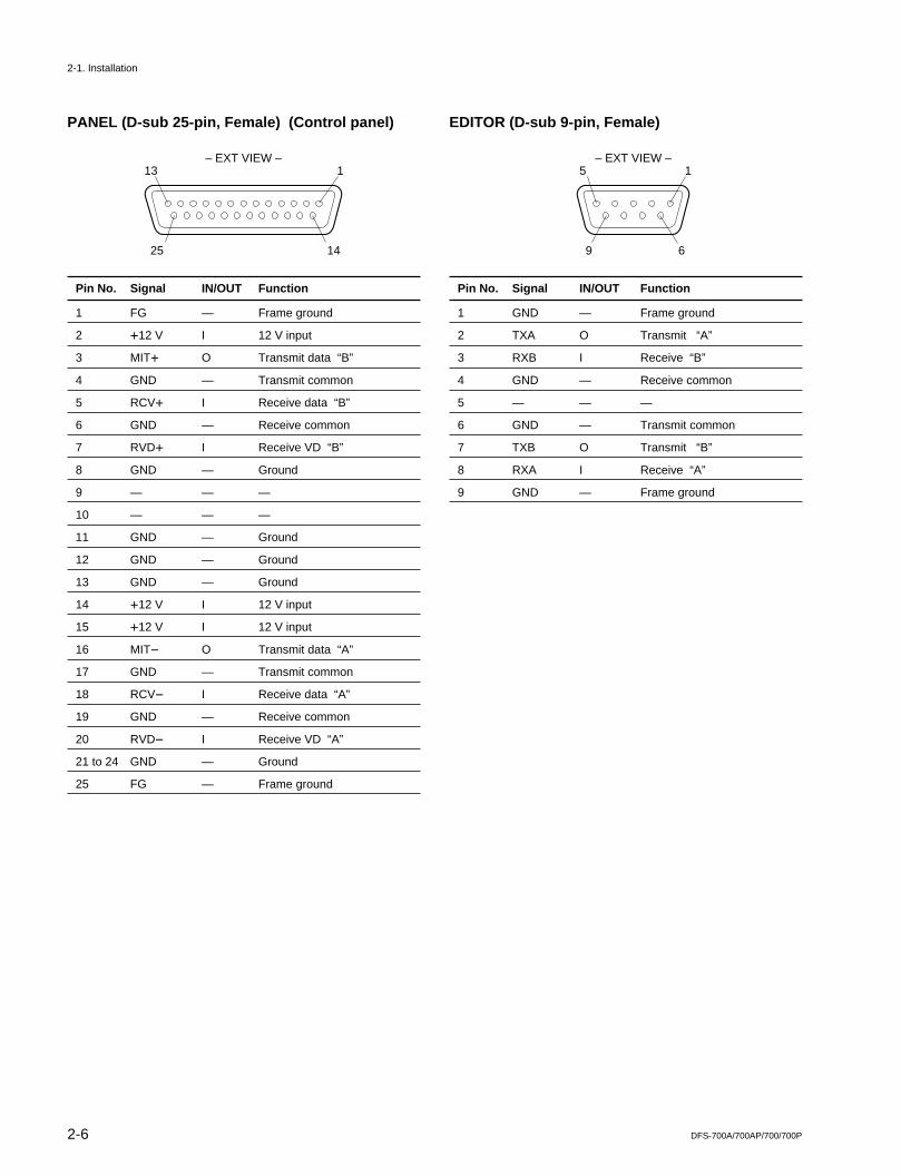
PANEL (D-sub 25-pin, Female) (Control panel)
Pin No. Signal IN/OUT Function
1 FG — Frame ground
2 +12 V I 12 V input
3 MIT+ O Transmit data “B”
4 GND — Transmit common
5 RCV+ I Receive data “B”
6 GND — Receive common
7 RVD+ I Receive VD “B”
8 GND — Ground
9 — — —
10 — — —
11 GND — Ground
12 GND — Ground
13 GND — Ground
14 +12 V I 12 V input
15 +12 V I 12 V input
16 MIT_ O Transmit data “A”
17 GND — Transmit common
18 RCV_ I Receive data “A”
19 GND — Receive common
20 RVD_ I Receive VD “A”
21 to 24 GND — Ground
25 FG — Frame ground
EDITOR (D-sub 9-pin, Female)
Pin No. Signal IN/OUT Function
1 GND — Frame ground
2 TXA O Transmit “A”
3 RXB I Receive “B”
4 GND — Receive common
5 — — —
6 GND — Transmit common
7 TXB O Transmit “B”
8 RXA I Receive “A”
9 GND — Frame ground
5 1
9 6
– EXT VIEW –13 1
25 14
– EXT VIEW –
2-1. Installation
2-7DFS-700A/700AP/700/700P
13 1
25 14
– EXT VIEW –
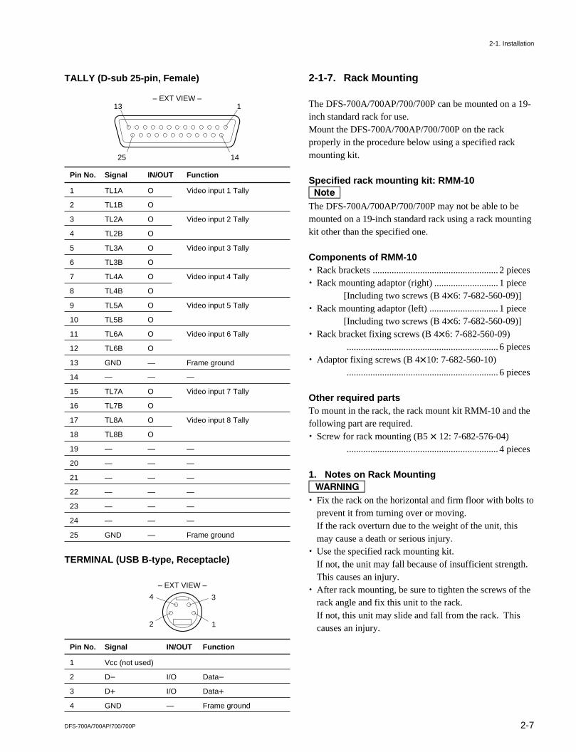
TALLY (D-sub 25-pin, Female)
Pin No. Signal IN/OUT Function
1 TL1A O Video input 1 Tally
2 TL1B O
3 TL2A O Video input 2 Tally
4 TL2B O
5 TL3A O Video input 3 Tally
6 TL3B O
7 TL4A O Video input 4 Tally
8 TL4B O
9 TL5A O Video input 5 Tally
10 TL5B O
11 TL6A O Video input 6 Tally
12 TL6B O
13 GND — Frame ground
14 — — —
15 TL7A O Video input 7 Tally
16 TL7B O
17 TL8A O Video input 8 Tally
18 TL8B O
19 — — —
20 — — —
21 — — —
22 — — —
23 — — —
24 — — —
25 GND — Frame ground
TERMINAL (USB B-type, Receptacle)
Pin No. Signal IN/OUT Function
1 Vcc (not used)
2 D_ I/O Data_
3 D+ I/O Data+
4 GND — Frame ground
2-1-7. Rack Mounting
The DFS-700A/700AP/700/700P can be mounted on a 19-inch standard rack for use.Mount the DFS-700A/700AP/700/700P on the rackproperly in the procedure below using a specified rackmounting kit.
Specified rack mounting kit: RMM-10nThe DFS-700A/700AP/700/700P may not be able to bemounted on a 19-inch standard rack using a rack mountingkit other than the specified one.
Components of RMM-10. Rack brackets ..................................................... 2 pieces. Rack mounting adaptor (right) ........................... 1 piece
[Including two screws (B 4x6: 7-682-560-09)]. Rack mounting adaptor (left) ............................. 1 piece
[Including two screws (B 4x6: 7-682-560-09)]. Rack bracket fixing screws (B 4x6: 7-682-560-09)
................................................................ 6 pieces. Adaptor fixing screws (B 4x10: 7-682-560-10)
................................................................ 6 pieces
Other required partsTo mount in the rack, the rack mount kit RMM-10 and thefollowing part are required.. Screw for rack mounting (B5 x 12: 7-682-576-04)
................................................................ 4 pieces
1. Notes on Rack Mountingw. Fix the rack on the horizontal and firm floor with bolts to
prevent it from turning over or moving.If the rack overturn due to the weight of the unit, thismay cause a death or serious injury.
. Use the specified rack mounting kit.If not, the unit may fall because of insufficient strength.This causes an injury.
. After rack mounting, be sure to tighten the screws of therack angle and fix this unit to the rack.If not, this unit may slide and fall from the rack. Thiscauses an injury.2
4 3
1
– EXT VIEW –
2-1. Installation
2-8 DFS-700A/700AP/700/700P
cAttention when this unit is installed in the rack:. Mount the unit with two or more persons.. Be careful not to put your hand or finger in the rack
mount rail.. Install in a stable posture.
nInstall a ventiloting fan in the rack to prevent the increasein the temperature inside a rack when multiple units are putin one rack.
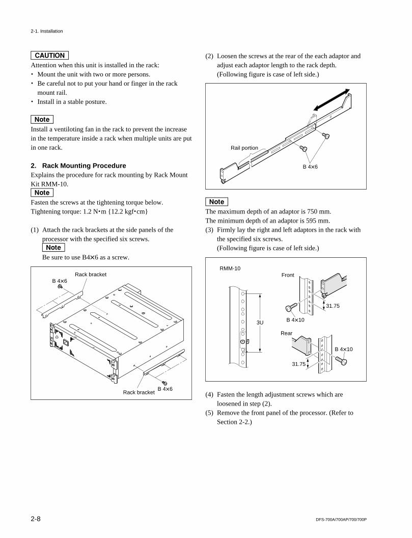
2. Rack Mounting ProcedureExplains the procedure for rack mounting by Rack MountKit RMM-10.nFasten the screws at the tightening torque below.Tightening torque: 1.2 N.m {12.2 kgf.cm}
(1) Attach the rack brackets at the side panels of theprocessor with the specified six screws.nBe sure to use B4x6 as a screw.
(2) Loosen the screws at the rear of the each adaptor andadjust each adaptor length to the rack depth.(Following figure is case of left side.)
nThe maximum depth of an adaptor is 750 mm.The minimum depth of an adaptor is 595 mm.(3) Firmly lay the right and left adaptors in the rack with
the specified six screws.(Following figure is case of left side.)
(4) Fasten the length adjustment screws which areloosened in step (2).
(5) Remove the front panel of the processor. (Refer toSection 2-2.)
Rack bracketB 4x6
Rack bracketB 4x6
B 4x6
Rail portion
Front
Rear
B 4x10³U
31.75
31.75
RMM-10
B 4x10
2-1. Installation
2-9DFS-700A/700AP/700/700P
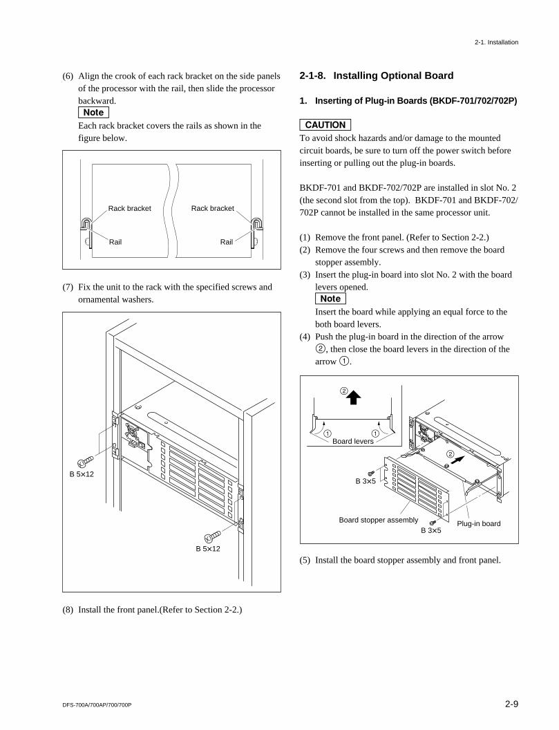
(6) Align the crook of each rack bracket on the side panelsof the processor with the rail, then slide the processorbackward.nEach rack bracket covers the rails as shown in thefigure below.
(7) Fix the unit to the rack with the specified screws andornamental washers.
(8) Install the front panel.(Refer to Section 2-2.)
2-1-8. Installing Optional Board
1. Inserting of Plug-in Boards (BKDF-701/702/702P)
cTo avoid shock hazards and/or damage to the mountedcircuit boards, be sure to turn off the power switch beforeinserting or pulling out the plug-in boards.
BKDF-701 and BKDF-702/702P are installed in slot No. 2(the second slot from the top). BKDF-701 and BKDF-702/702P cannot be installed in the same processor unit.
(1) Remove the front panel. (Refer to Section 2-2.)(2) Remove the four screws and then remove the board
stopper assembly.(3) Insert the plug-in board into slot No. 2 with the board
levers opened.nInsert the board while applying an equal force to theboth board levers.
(4) Push the plug-in board in the direction of the arrow2, then close the board levers in the direction of thearrow 1.
(5) Install the board stopper assembly and front panel.
B 5x12
B 5x12
B 3x5Board stopper assembly
Board levers
Plug-in board
B 3x5
1
2
2
1
2-1. Installation
Rail Rail
Rack bracket Rack bracket
2-10 DFS-700A/700AP/700/700P
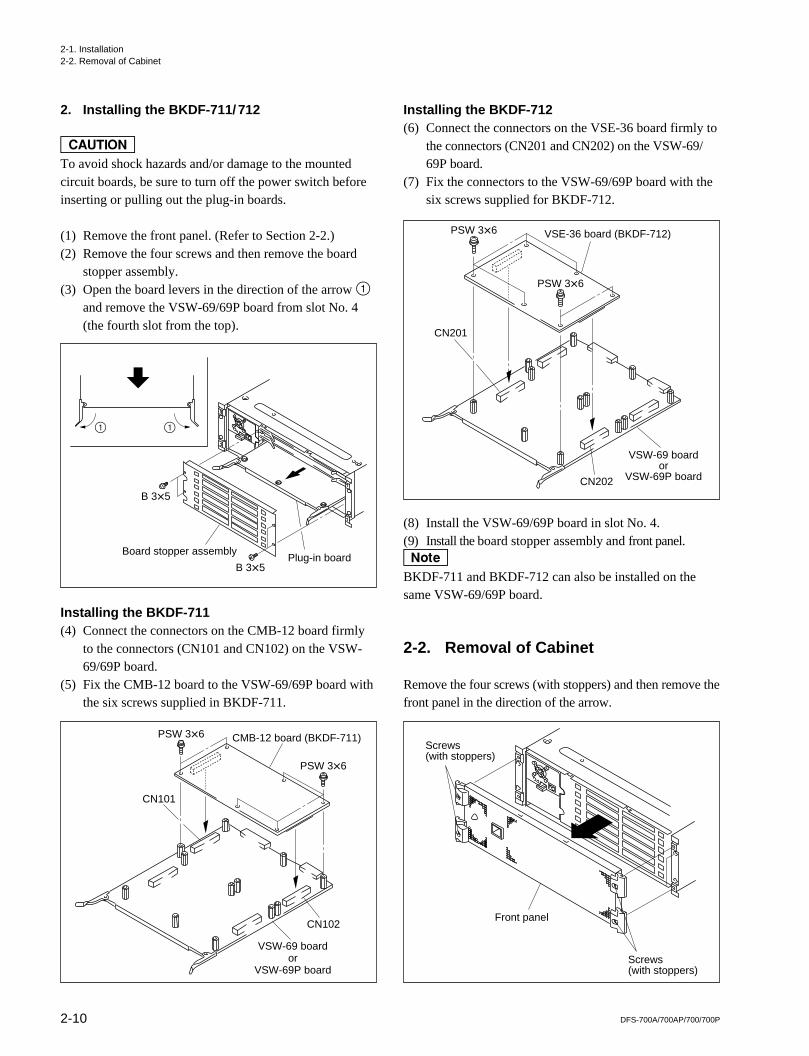
Installing the BKDF-712(6) Connect the connectors on the VSE-36 board firmly to
the connectors (CN201 and CN202) on the VSW-69/69P board.
(7) Fix the connectors to the VSW-69/69P board with thesix screws supplied for BKDF-712.
(8) Install the VSW-69/69P board in slot No. 4.(9) Install the board stopper assembly and front panel.nBKDF-711 and BKDF-712 can also be installed on thesame VSW-69/69P board.
2-2. Removal of Cabinet
Remove the four screws (with stoppers) and then remove thefront panel in the direction of the arrow.
B 3x5
Board stopper assemblyPlug-in board
B 3x5
1 1
2. Installing the BKDF-711/ 712
cTo avoid shock hazards and/or damage to the mountedcircuit boards, be sure to turn off the power switch beforeinserting or pulling out the plug-in boards.
(1) Remove the front panel. (Refer to Section 2-2.)(2) Remove the four screws and then remove the board
stopper assembly.(3) Open the board levers in the direction of the arrow 1
and remove the VSW-69/69P board from slot No. 4(the fourth slot from the top).
Installing the BKDF-711(4) Connect the connectors on the CMB-12 board firmly
to the connectors (CN101 and CN102) on the VSW-69/69P board.
(5) Fix the CMB-12 board to the VSW-69/69P board withthe six screws supplied in BKDF-711.
PSW 3x6
PSW 3x6 CMB-12 board (BKDF-711)
CN101
CN102
VSW-69 boardor
VSW-69P board
PSW 3x6
PSW 3x6 VSE-36 board (BKDF-712)
CN201
CN202
VSW-69 boardor
VSW-69P board
Front panel
Screws(with stoppers)
Screws(with stoppers)
2-1. Installation2-2. Removal of Cabinet
2-11DFS-700A/700AP/700/700P
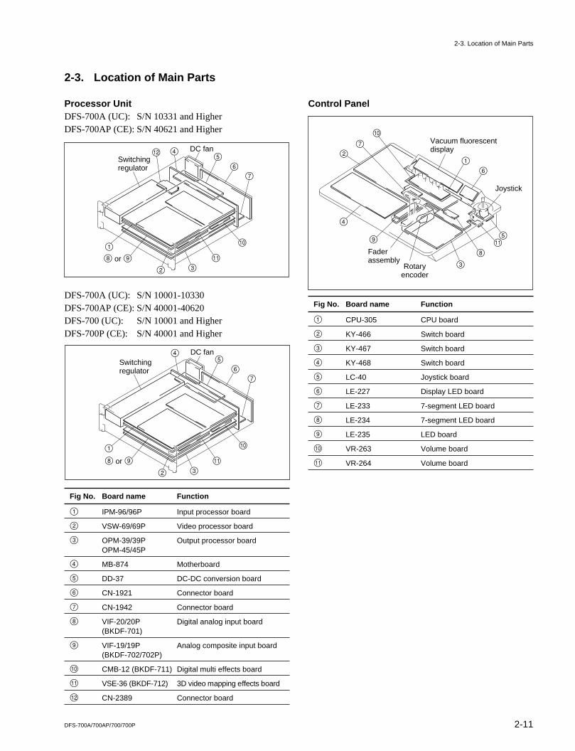
2-3. Location of Main Parts
Processor UnitDFS-700A (UC): S/N 10331 and HigherDFS-700AP (CE): S/N 40621 and Higher
DFS-700A (UC): S/N 10001-10330DFS-700AP (CE): S/N 40001-40620DFS-700 (UC): S/N 10001 and HigherDFS-700P (CE): S/N 40001 and Higher
Fig No. Board name Function
1 IPM-96/96P Input processor board
2 VSW-69/69P Video processor board
3 OPM-39/39P Output processor boardOPM-45/45P
4 MB-874 Motherboard
5 DD-37 DC-DC conversion board
6 CN-1921 Connector board
7 CN-1942 Connector board
8 VIF-20/20P Digital analog input board(BKDF-701)
9 VIF-19/19P Analog composite input board(BKDF-702/702P)
0 CMB-12 (BKDF-711) Digital multi effects board
!- VSE-36 (BKDF-712) 3D video mapping effects board
!= CN-2389 Connector board
Control Panel
Fig No. Board name Function
1 CPU-305 CPU board
2 KY-466 Switch board
3 KY-467 Switch board
4 KY-468 Switch board
5 LC-40 Joystick board
6 LE-227 Display LED board
7 LE-233 7-segment LED board
8 LE-234 7-segment LED board
9 LE-235 LED board
0 VR-263 Volume board
!- VR-264 Volume board
Switchingregulator
DC fan45
67
32
1
8 or 9 !-
0
27
0Vacuum fluorescentdisplay
16
Joystick
5!-
83Rotary
encoder
Faderassembly
9
4
2-3. Location of Main Parts
Switchingregulator
4 DC fan5
67
32
18 or 9 !-
!=
0
2-12 DFS-700A/700AP/700/700P
2-4. Circuit Description
2-4. Circuit Description
2-4-1. Processor
1. CMB-12 Board (2 Channel Digital Multi-effect Board)
V2 (FRGD) and K2 (TITLE) signals are processed on the CMB-12 board.
The V2 signal is used as an FRGD signal so as to perform the color collector processing, border addition,beveled edge addition, and two-dimensional low-pass filter processing.In the title mode, the K2 signal is used as a key signal. After key processing, the key signal is used as awipe key by a wipe generator so as to transform the two-dimensional low-pass filter processing. After theprocessing, the FRGD and key signals are written in DME memory. For the read address of DMEmemory data, the generator circuit varies depending on the two types of effects below.(1) 2D, 3D nonlinear effect(2) 3D mapping effect (when the VSE-36 board is installed)The read data is interpolated for lighting. The data is then combined using the key signal from the VSW-69/69P board and the key signal processed on the CMB-12 board. The resultant FRGD and key signalsare sent to the VSW-69/69P board.
2. DD-37 Board (DC-DC Converter)
In the DD-37 board, a power supply of +12 V is converted into the voltage used in each circuit.The 12 V power supply output from an AC-DC power unit is converted into the voltages (+5 V, +3.3 V,+7 V, and _7 V) required in each circuit.
IC3, IC4, and IC5 are dual switching regulator control ICs. One IC can control two power outputs. IC3controls +5 V-1 and +5 V-2 outputs, and IC4 controls +5 V-3 and +3.3 V-2 outputs. IC5 controls +7 Vand _7 V outputs. For the maximum load current of each output voltage, +5 V and +3.3 V are 10 A, and+7 V and _7 V are 3 A.
3. IPM-96/96P Board (Input Processor Board)
The IPM-96/96P board is used to input the SDI, component (Y, R-Y, B-Y), and component (RGB)signals for DFS-700A/700AP/700/700P. The IPM-96/96P board mounts a four-channel SDI circuit andfour-channel component circuit. A video signal is sent to the BG and FG buses by the switching of acrosspoint.
The IPM-96/96P board accepts three input signals; SDI signals (270 Mbps), component (Y, R-Y, B-Y)signals, and component (RGB) signals. Four-channel SDI signals, four-channel component (Y, R-Y, B-Y) signals, and RGB signals can be assigned to channels 1 through 8 of a crosspoint. For the one-channelanalog signal input to the 8/4 component input connector, a component (Y, R-Y, B-Y) signal orcomponent (RGB) signal is selected according to the format.(1) Signal input block
An SDI input signal is directly converted into 4:2:2 parallel signal of an eight-bit by an SDI input ICand sent to the next stage.For a component signal input, an RGB-to-Y, R-Y, B-Y conversion circuit is added to only the 8/4input connector. The analog component signal can be input based on an RGB or Y, R-Y, B-Y signalsystem by the selection of a format. As a result, all analog input signals become Y, R-Y, B-Y signals.
2-13DFS-700A/700AP/700/700P
2-4. Circuit Description
In each channel, these signals are analog-to-digital converted by the same circuit processing systemand sent to the next stage as 4:2:2 parallel signal of an eight-bit.
(2) Analog input blockThe analog input block on the IPM-96/96P board can accept four-channel component input signal.Basically, the analog input block receives Y, R-Y, and B-Y signals. Only the fourth channel isprovided with an RGB-to-Y, R-Y, B-Y conversion circuit and selection circuit so that it can alsoreceive an RGB component signal. Therefore, the circuit stage after the selection circuit in the fourthchannel is the same in each channel. Only the first channel is described below as an example.A Y signal is passed through a 5.5 MHz low-pass filter, converted into the proper value in a signallevel, and fed to the A/D converter by AC coupling. Color difference signals R-Y and B-Y arepassed through a Y/C delay adjustment circuit and 2.5 MHz low-pass filter, converted into the propervalue in level, and sent to the A/D converter by AC coupling. A/D converter IC107 is an eight-bit Y,R-Y, B-Y simultaneous conversion output circuit incorporating a clamp function. In the case ofreference voltage for A/D conversion, a top voltage of 3.5 V and a bottom voltage of 1.5 V aresupplied using a reference voltage generator circuit and operational amplifier. For the phase relationat the input end of the A/D converter, a Y signal is supplied in the state where it is advanced 222 ns(corresponding to three clocks of a 13.5 Mbps digital clock) with respect to a R-Y, B-Y signal. Whenthe Y signal is converted into a digital signal, only the Y signal is delayed by three clocks (222 ns) forphase adjustment. Since the Y signal has a high frequency band, the delay in an analog circuit isdisadvantageous in frequency characteristics and is processed by a digital circuit. Moreover, thedigital output Y signal of the A/D converter is converted in a digital level by a ROM table so as toselect the level difference in NTSC-J, NTSC-UC, and PAL. The level is converted (expanded) forNTSC-UC only.
(3) Input conversion clock generation blockEach input circuit requires a 4:2:2 digital clock (13.5 MHz) synchronized with an input analog signal.Therefore, each channel has a clock generator circuit in the input block. The signal just beforeentering the A/D converter is taken out from the Y signal system of an input signal and compositesync information is extracted using a sync separator circuit. One of the extracted informationgenerates a clamp pulse for clamping an input signal. The other is passed through a half H killercircuit and then connected to a clock generation PLL circuit of 27 MHz via the video phaseadjustment circuit during digital conversion. As a result, clocks of 27 MHz and 13.5 MHz and Hstart pulses are generated.
(4) Digital level conversion blockOn the IPM-96/96P board, the input level is multiplied by 1.08 (expanded in level proportionally tothe setup elimination) in the NTSC-UC mode using a ROM table after A/D conversion. This is thelevel conversion by digital processing. Using this system, the setup elimination can also besimultaneously processed without changing the clamp operation and function required until the A/Dconverter is used. This system is thus very efficient. The DFS-700A/700AP/700/700P is designed sothat data completely returns to the former state between the input and output (expansion to reduction)and coincides with each other. Therefore, this ensures the satisfactory characteristics of waveforms.
(5) TBC blockAfter an SDI input signal is converted from serial to parallel, it is input to the line memory. After acomponent input signal is converted from analog to digital, it is input to the line memory. In this linememory, the TBC block having a lead-in range of _0.3 to +1.3 H from a REF signal as reference isconstituted. On the write side, the line memory is written in the phase of an input signal. On the readside, it is read in the lead-in timing described above. As a result, on the read side, all input channels areadjusted to the same phase. Similarly, after a component input signal is converted from analog todigital, all channels become in phase with an SDI input by the output of line memory. The write andread control signals of the line memory are generated based on internal HD and VD pulses usingmemory control circuits (IC1320 to IC1323, IC1330, and IC1331).
2-14 DFS-700A/700AP/700/700P
2-4. Circuit Description
(6) Crosspoint blockThe input signal of a crosspoint on the IPM-96/96P board is a four-channel SDI input signal and four-channel component input signal. When the VIF-20/20P board is installed, the four-channel SDI inputsignal or four-channel component signal of the VIF-20/20P board is used as the input signal of acrosspoint. When the VIF-19/19P board is installed, the four-channel composite input signal or four-channel S video input signal of the VIF-19/19P board, and a memory bus and internal video signal areused as the input signal of a crosspoint. The output signal of a crosspoint is V1, K1, V2, K2, V3, andBG buses passed to the VSW-69/69P board, a DSKF bus passed to the OPM board (OPM-39/39P orOPM-45/45P), and a memory bus used as the input signal of the frame memory on the IPM-96/96Pboard.
(7) Frame memory blockThe frame memory block freezes an input signal. The frozen video signal is used as one of the inputsignals in a crosspoint. When the input signal selected at the crosspoint is input from the memory bus tothe frame memory circuit, it is separated into luminance and color-difference signals and written in theframe memory. The frame memory consists of four field memories and memorizes the luminance andcolor-difference signals separately in units of fields. After the luminance and color-difference signalsare read, they are multiplexed and then output. For frame freezing, the luminance and color-differencesignals are alternately read from memory in units of fields. For field freezing, odd and even fieldfreezes are available. One field is read at all times. In the other field, two lines are added forinterpolation. A two-line addition line buffer (IC1209) and adder (IC1208) are used as this circuit. Thecontrol signal of the frame memory is generated based on internal FD and VD pulses using memorycontrol circuits (IC1322, IC1324, IC1326, and IC1333).
(8) CPU interface blockThe IPM-96/96P board sets the mode selection or initial value by communicating with CPU (IC901) onthe VSW-69/69P board. After IC1327 receives the data, address, and control signal from CPU anddecodes them, it sends a chip select and set value to the SIF control circuit.
4. OPM-39/39P or OPM-45/45P Board (Output Processor Board)
The OPM-39/39P or OPM-45/45P board (abbreviated as OPM board hereafter) outputs the DME, PVW,and KEY signals input from the VSW-69/69P board as an SDI or analog (component, S video, orcomposite) format signal. The OPM board mounts a DSK circuit that mixes a DSK video signal with theDME signal. This board also has an external reference sync circuit and black burst output circuit as wellas an internal sync generator.
The OPM board consists of the following blocks.(1) Gen-lock/system clock
This block generates the reference signals required for DFS-700A/700AP/700/700P, such as internalsignals (FD, VD, HD, BLK, CKF (27 MHz), and CKM (13.5 MHz) or an external output black burstsignal.Each output signal operates with the sync signal of a sync generator (IC103) as the source. In theoperation mode, there are an EXTERNAL GEN-LOCK mode that is gen-locked to the sync signal(VBS or BS) supplied from an external signal oscillator and an INTERNAL mode that internallygenerates a sync signal. When a sync signal is sent to the REF. VIDEO input connector on the rearpanel, the unit automatically enters the EXTERNAL GEN-LOCK mode.
2-15DFS-700A/700AP/700/700P
(2) DSK (Down Stream Keyer)This block generates the key signal required for mixing a DME signal and DSK video signal.In addition to the component key signal input from the DSK KEY input connector on the rear panel,the self-key obtained when only a Y signal is extracted from a DSK fill signal can also be selected fora DSK source signal. The DSK source signal is adjusted in gain and clip, and masked, using a keyprocessor (IC303). A fill key (FLK) signal that mixes the DSK fill signal with a border mat signaland a downstream key (DK) signal that is required for mixing with the DME signal are generated inthe next-stage border processor (IC310) using a five-line key signal.The OPM-45/45P board adjusts the position of keying characters, etc. (DSK) by changing the delayamount using IC301, IC410 and IC411.
(3) DSK M/E, FTBThe mixing operation of a DME signal and DSK video signal, and the FTB (feed-to-black) operationare performed in this block.A DSK fill (or DSK mat) signal and border mat signal are first mixed with the fill key signal used asa coefficient. The PGM signal obtained when a DSK video signal with border is inserted into theDME signal is produced by this processing. The PGM signal is mixed for performing the FTBoperation to a color mat signal and sent to the SDI and analog output circuit blocks. The signals(CLEAN, PVW, and KEY) output to the CLEAN connector are also selected by this block.
(4) OUTPUTThis block outputs PGM, CLEAN, PVW, and KEY signals as an SDI or analog format signal.In an SDI output system, there are a PGM signal and a signal output to the CLEAN connector. AfterV BLANKING addition and WHITE/DARK clipping are performed via this path using outputprocessors (IC408 and IC504), these signals are converted from parallel to serial and then output.There are PGM and PVW signals in an analog output system. In the PGM path, a (eight-bit, 27MHz) digital signal is separated into Y, V, and U signals and converted into an analog signal using aD/A converter. On the basis of the converted signal, component, S video, and composite signals areproduced for output. Unlike the PGM path, in the PVW path, a digital signal is converted into acomposite signal by one LSI (IC808).The following signals can be output from the output connector on the rear panel according to thesignal formats below.
PGM output signal SDI signal 2 channelsComponent signal 2 channelsComposite signal 2 channelsS video signal 2 channels
PVW output signal Composite signal 1 channelCLEAN output signal SDI signal 1 channel
(CLEAN, PVW, or KEY signal)Black burst output signal 3 channelsTally output signal 8 outputs
(5) CPU interfaceThis block interfaces with the IC and local CPU on the OPM board.This block decodes the control signal generated by CPU using FPGA (IC805) and generates a controlsignal according to the way to control the IC. It also passes the information on the NTSC/PALdistinction and NTSC J/NTSC UC model to CPU via FPGA.
2-4. Circuit Description
2-16 DFS-700A/700AP/700/700P
2-4. Circuit Description
5. VIF-19/19P Board (Analog Composite and S Video Input Board)
The VIF-19/19P board is used for inputting the analog composite and S video signals of DFS-700A/700AP/700/700P. The VIF-19/19P board decodes the input composite signal and converts it into a D1digital signal. This board also has a frame synchronizer function and uses an input signal as the signalsynchronized with a reference signal. The output signal is sent to the IPM-96/96P board.The VIF-19/19P board mounts a four-channel analog composite or S video input circuit. In each channel,an analog composite input signal or S video input signal can be independently selected in the setup menu.One channel is described below.
The circuit consists of a sync separator circuit, 13.5-MHz clock generation block, subcarrier clockgeneration block, Y/C separation and decode block, D1 encoder block, and frame synchronizer block.
The analog composite and S video input signals have an individual input connector on the rear panel.These signals can be simultaneously input to the VIF-19/19P board. On the VIF-19/19P board, two inputsignals are selected by controlling the setup menu.
The selected signal branches into two paths. One is input to the sync separation circuit so as to detecthorizontal and vertical sync signals. After that, in the 13.5-MHz clock generation block, the signalgenerates a 13.5-MHz clock for the D1 signal synchronized with a horizontal sync signal.
The other is input to the Y/C separation and decode circuit. In the subcarrier clock generation block, thesignal generates the clock of the subcarrier frequency, multiplied by four, that was synchronized with aburst signal. After that, a composite signal is converted from analog to digital, Y/C-separated, anddecoded by this clock. The resultant signal is converted from digital to analog again to produce an analogcomponent signal. The Y/C separation is based on an adaptive two-dimensional system in which threelines are used. For the S video signal, only a chroma signal is converted from analog to digital anddecoded digitally by this clock. The resultant signal is converted from digital to analog again to produceanalog B-Y and R-Y signals. For a Y signal, the input analog signal is used directly.
The analog component signal is adjusted in phase and gain and converted from analog to digital using the13.5-MHz clock described above to produce a D1 digital signal.
A frame synchronizer is constituted for each signal Y and C. The frame synchronizer consists of two FIFOs of384 K x 8 bits, respectively. The signals are written in FIFO using the clock synchronized with an input signaland read using the clock synchronized with a reference signal. The input signal synchronized with areference signal is delayed by about 1 to 3 H in this portion, but absorbed by other boards. Therefore, inthe system, the delay will not increase by passing through the frame synchronizer.
6. VIF-20/20P Board (SDI and Analog Component Input Board)
The VIF-20/20P board is an optional expansion board for inputting the SDI and analog componentsignals of DFS-700A/700AP/700/700P. The VIF-20/20P board mounts a four-channel SDI input circuitor four-channel analog component input circuit. The SDI or analog component input signal is sent to theIPM-96/96P board as a four-channel 4:2:2 component parallel digital signal. In each channel, the SDIinput signal or analog component input signal can be independently selected according to the format.
2-17DFS-700A/700AP/700/700P
2-4. Circuit Description
(1) Signal input blockThere are four channels in an SDI input circuit. An SDI input signal is directly converted into an eight-bit,4:2:2 parallel signal. There are also four channels in a component input circuit. Finally, the signals in eachchannel are converted into eight-bit, 4:2:2 parallel signals by the same circuit system. The signals in fourchannels are selected together with the signal from the SDI input circuit and sent to the next-stage TBC circuit.The analog component input circuit generates a clock of 27 MHz synchronized with an input signal,regulates the level and delay value, and converts the signal from analog to digital.
(2) Analog input blockThe analog input block on the VIF-20/20P board is basically almost the same in configuration as forthe IPM-96/96P board. The circuit configuration is almost the same as that obtained when acomponent (RGB) signal input converter added to only the fourth channel is removed from the circuitconfiguration of the IPM-96/96P board and when a level selection circuit for each signal format isinserted into each four-channel color-difference (R-Y and B-Y) signal system. Therefore, therelevant circuit configuration is explained below. For other configuration, refer to “(2) Analog InputBlock” of the IPM-96/96P board.A video selection circuit of 3 x 1 is inserted in each four-channel color-difference signal system. Onthe input side, a chroma signal is precisely divided by a high-precision resistor so as to select thelevel using a selection signal and sent to the next stage. In the case of the chroma signal, the inputlevel for making the same in level as 75% color bars of an SDI signal is 756 mV for NTSC J, 700mV for NTSC UC, and 525 mV for PAL. As a result, the system operates so that the output level ofa selector circuit is constant in any input level. This shows that the setting of a chroma signal leveldoes not vary depending on the format used.
(3) Input conversion clock generation blockEach input circuit requires a 4:2:2 digital clock (13.5 MHz) synchronized with an input analog signal.Therefore, each channel has a clock generator circuit in the input block. The signal just before enteringthe A/D converter is taken out from the Y signal system of an input signal and composite syncinformation is extracted using a sync separator circuit. One of the extracted information generates aclamp pulse for clamping an input signal. The other is passed through a half H killer circuit and thenconnected to a clock generation PLL circuit of 27 MHz via the video phase adjustment circuit duringdigital conversion. As a result, clocks of 27 MHz and 13.5 MHz and H start pulses are generated.
(4) Digital level conversion blockOn the VIF-20/20P board, the input level is multiplied by 1.08 (expanded in level proportionally tothe setup elimination) in the NTSC-UC mode using a ROM table after A/D conversion. This is thelevel conversion by digital processing. Using this system, the setup elimination can also besimultaneously processed without changing the clamp operation and function required until the A/Dconverter is used. This system is thus very efficient. The DFS-700A/700AP/700/700P is designed sothat data completely returns to the former state between the input and output (expansion to reduction)and coincides with each other. Therefore, this ensures the satisfactory characteristics of waveforms.
(5) TBC blockAfter an SDI input signal is converted from serial to parallel, the video signal selected according tothe format is input to the line memory. After a component input signal is converted to analog todigital, the video signal selected according to the format is input to the line memory. In this linememory, the TBC block having a lead-in range of _0.3 to +1.3 H from a REF signal as reference isconstituted. On the write side, the line memory is written in the phase of an input signal. On the readside, it is read in the lead-in timing described above. As a result, on the read side, all input channelsare adjusted to the same phase. Similarly, after a component input signal is converted from analog todigital, all channels are adjusted to the same phase by the output of line memory. The write and readcontrol signals of the line memory are generated based on internal HD and VD pulses using memorycontrol circuits (IC1309, IC1320, IC1321, and IC1323). The output video signal of the TBC block issent to the IPM-96/96P board and input to the crosspoint.
2-18 DFS-700A/700AP/700/700P
2-4. Circuit Description
(6) CPU interface blockThe VIF-20/20P board sets the mode selection or initial value by communicating with CPU (IC901) onthe VSW-69/69P board. After IC1327 receives the data, address, and control signal from CPU anddecodes them, it sends a chip select and set to the SIF control circuit.
7. VSE-36 Board (3D Mapping Effects Board)
The VSE-36 board is used to realize a three-dimensional mapping effect. This board consists of anaddress generation block and texture memory block.
The address generation block can be divided into a CPU block and rendering block. The CPU blockconsists of CPU (IC501), program flash memories (IC601 to IC605), SDRAMs (IC612, IC613, IC615,IC616), and dual port RAM (IC510). The rendering block consists of DDA (IC401), address memories(IC413 to IC420) and address memory controllers (IC105, IC106, and IC109).
The CPU block receives the information (e.g., system set information, effect pattern number, faderposition, etc.) required for effect generation from the main CPU on the VSW-69/69P board via dual portRAM and transforms the three-dimensional object creation, geometry processing, and lighting calculationfor each vertex.
The rendering block expands the vertex data from a CPU (IC901) block to the information based on unitsof pixels by DDA and draws it on the address memory. The address memory controller reads the drawnaddress information and sends it to the texture memory block on the VSE-36 board, or the VSW-69/69Pand CMB-12 boards. The address memory has a double-buffer configuration. Therefore, drawing andreading are alternately switched for each field.
The texture memory block consists of a demultiplexer (IC105), color collector (IC251), border mixer(IC253), low-pass filters (IC201 and IC208), texture memory controllers (IC301 and IC306), and texturememories (IC302 to IC305, and IC307 to IC310).In the texture memory block, color collector processing, border addition, and two-dimensional low-passfilter processing are performed for the V3 signal (8-bit, 27 MHz) sent from the VSW-69/69P board as atexture video source. After that, the signal is written in texture memory. The texture memory controllerreads the written data using the address generated by an address generation block, interpolates the data,and send it to the VSW-69/69P board. The texture memory has a double-buffer configuration. Therefore,writing and reading are alternately switched for each field.
8. VSW-69/69P Board (Processor Board)
The VSW-69/69P board consists of a signal processing block and CPU block. This board transforms theDME processing according to the control panel operation.V1, K1, BG, V2, K2, and V3 signals (8-bit, 27 MHz) are input from the IPM-96/96P board to the VSW-69/69P board.The signal processing block processes the V1, K1, and BG signals and outputs PGM, KEY, and PVWsignals to the OPM board (OPM-39/39P or OPM-45/45P).The V1 signal is used as an FRGD signal so as to transform the color collector processing, borderaddition, beveled edge addition, and two-dimensional low-pass filter processing.
2-19DFS-700A/700AP/700/700P
2-4. Circuit Description
In the title mode, the K1 signal is used as a key signal. After key processing, the K1 signal is used as awipe key by a wipe generator so as to perform the two-dimensional low-pass filter processing.The FRGD and key signals in which the two-dimensional low-pass filter processing was carried out arewritten in DME memory. For the read address of DME memory data, the generator circuit variesdepending on the three types of effects below. (1) 2D, 3D, and nonlinear effects (2) Sparkle effect (3) 3D-mapping effect (when the VSE-36 board is mounted)The read data is interpolated for lighting.The signal immediately after lighting for luminance and chroma signals and the signal immediately afterinterpolation for a key signal are sent to the VSW-69/69P board’s later stage and the CMB-12 board inparallel.The resultant signal is passed through a selection circuit and trailing block for the signal from the optionalCMB-12 board. In a specific effect, the signal is then given later-stage wiping and later-stage borderprocessing and mixed with a BKGD signal.The signal that gave color collector processing to a BG signal and of which phase was adjusted to anFRGD signal via field memory is used as the BKGD signal.
The CPU block consists of CPU (IC901), a program, data flash memories (IC920 to IC924, IC941,IC942), SDRAMs (IC909 and IC910), dual port memory (IC912), SRAM (IC911), and a USB controller(IC932). The SRAM is backed up by a capacitor, storing the crosspoint state, effect parameters, orsnapshot data.The CPU block calculates the register set value of hardware from each effect parameter and writes it inthe specified position inside the dual port memory. Moreover, the CPU block sets hardware with respectto the IPM-96/96P, OPM-39/39P or OPM-45/45P, VIF-19/19P, and VIF-20/20P boards.The CPU block also communicates with the external equipment such as a control panel, edit controller,and personal computer using a 2-channel serial port and USB interface.
2-4-2. Control Panel
1. CPU-305 Board
The CPU-305 board is the system control board on the control panel of DFS-700A/700AP/700/700P.The CPU-305 board communicates with a processor unit via RS-422, scans switches, and displaysindication elements such as LED/VFD (vacuum fluorescent display). The CPU-305 board mainlyconsists of the following circuit blocks.. CPU and CPU’s peripheral circuit. DC-DC converter block. External communication interface block. Switch scan/LED lighting interface block. Parallel interface block
(1) CPU and CPU’s peripheral circuitCPU uses a 16-bit microprocessor (IC21) in a clock of 16 MHz. CPU consists of 4 M-bit flashmemory (IC51) in which a boot loader is stored, 4 M-bit flash memory (IC54) in which systemcontrol software is stored, two 512 k-bit work SRAMs (IC52 and IC53), and an address decoder(IC26) that generates memories, parallel interface chip select signals, or read/write control signals.
2-20 DFS-700A/700AP/700/700P
2-4. Circuit Description
(2) DC-DC converter blockPowers of +5 V and +7 V are produced from +12 V, that is input from a processor unit, using theDC-DC converter (IC29). The +7 V power is passed through the KY-466 board and used to drivethe green and red LEDs inside large switches on the KY-467 and KY-468 boards.
(3) External interface blockThe external interface block communicates with a processor unit from the serial port (TXD0/RXD0)inside CPU via an RS-422 transceiver (IC24).
(4) Switch scan/LED lighting interface blockThis block controls the data scanning of switches, volume controls, joysticks, and faders on the KY,VR, and LC boards and the lighting of LEDs on the LED board.This block consists of 2 k-bit dual port memory (IC64), a dual port memory controller (IC70),parallel-to-serial converters (IC65 and IC66), a serial-to-parallel converter (IC68), and a buffer(IC67). The lighting on/off data of LEDs as well as the scan data of switches is memory-mapped onthe dual port memory from CPU.CPU writes the lighting on/off data of LEDs in the corresponding address of the dual port memory.The contents of the data are converted from parallel to serial (using IC65 and IC66) and sent to theKY-466 board together with a clock and other control signals.The scan data by which various switches were multiplexed is loaded from the KY-466 board in serialand converted from serial to parallel (using IC68). The converted data is loaded to the dual portmemory and read by CPU.
(5) Parallel interface blockUsing a parallel interface circuit (IC72), this block drives the buzzer and operating indication LEDs,reads the DIP switch information, and controls the dual port memory controller. Moreover, itcontrols and displays the vacuum fluorescent display through IC62 and IC63.
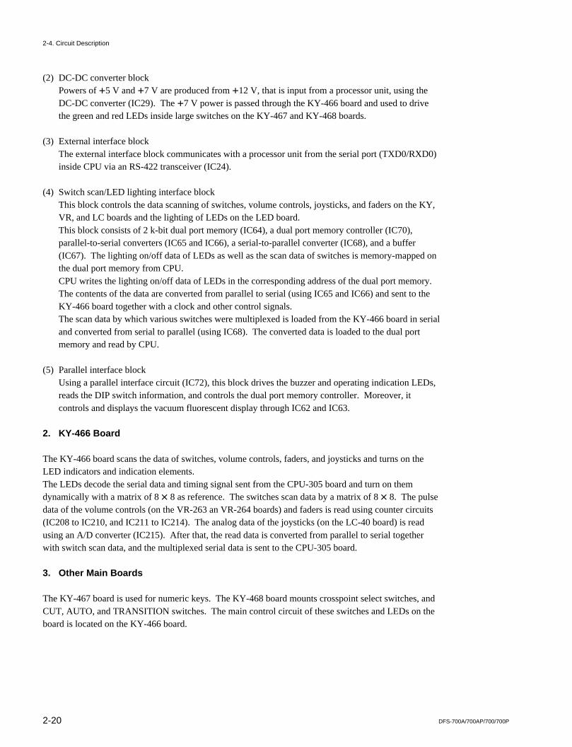
2. KY-466 Board
The KY-466 board scans the data of switches, volume controls, faders, and joysticks and turns on theLED indicators and indication elements.The LEDs decode the serial data and timing signal sent from the CPU-305 board and turn on themdynamically with a matrix of 8 x 8 as reference. The switches scan data by a matrix of 8 x 8. The pulsedata of the volume controls (on the VR-263 an VR-264 boards) and faders is read using counter circuits(IC208 to IC210, and IC211 to IC214). The analog data of the joysticks (on the LC-40 board) is readusing an A/D converter (IC215). After that, the read data is converted from parallel to serial togetherwith switch scan data, and the multiplexed serial data is sent to the CPU-305 board.
3. Other Main Boards
The KY-467 board is used for numeric keys. The KY-468 board mounts crosspoint select switches, andCUT, AUTO, and TRANSITION switches. The main control circuit of these switches and LEDs on theboard is located on the KY-466 board.
2-21DFS-700A/700AP/700/700P
2-5. Replacement of Board
cTo avoid shock hazards and/or damage to the mountedcircuit boards, be sure to turn off the power switch beforeinserting or pulling out the plug-in boards.
2-5-1. Replacement of Plug-in Board
1. Remove the front panel. (Refer to Section 2-2.)2. Remove the four screws and then remove the board
stopper assembly.3. Open the board levers in the direction of arrow 1 and
remove the plug-in board.
4. Install a new plug-in board in the reverse order of steps1 to 3.
B 3x5
Board stopperassembly Plug-in board
B 3x5
1 1
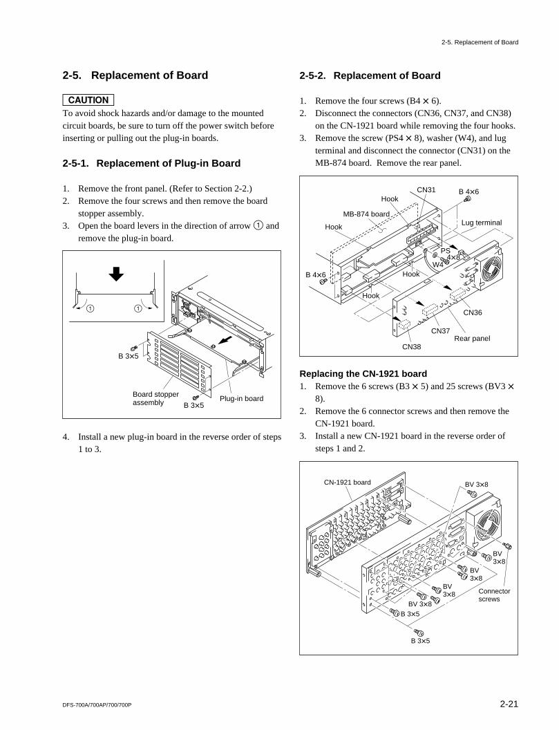
2-5-2. Replacement of Board
1. Remove the four screws (B4 x 6).2. Disconnect the connectors (CN36, CN37, and CN38)
on the CN-1921 board while removing the four hooks.3. Remove the screw (PS4 x 8), washer (W4), and lug
terminal and disconnect the connector (CN31) on theMB-874 board. Remove the rear panel.
Replacing the CN-1921 board1. Remove the 6 screws (B3 x 5) and 25 screws (BV3 x
8).2. Remove the 6 connector screws and then remove the
CN-1921 board.3. Install a new CN-1921 board in the reverse order of
steps 1 and 2.
2-5. Replacement of Board
B 4x6
B 4x6CN31
CN38
CN37
CN36
Rear panel
Lug terminal
W4Hook
Hook
Hook
MB-874 board
Hook
PS 4x8
B 3x5
B 3x5
BV 3x8
BV3x8
BV3x8
BV3x8
Connectorscrews
CN-1921 board BV 3x8
2-22 DFS-700A/700AP/700/700P
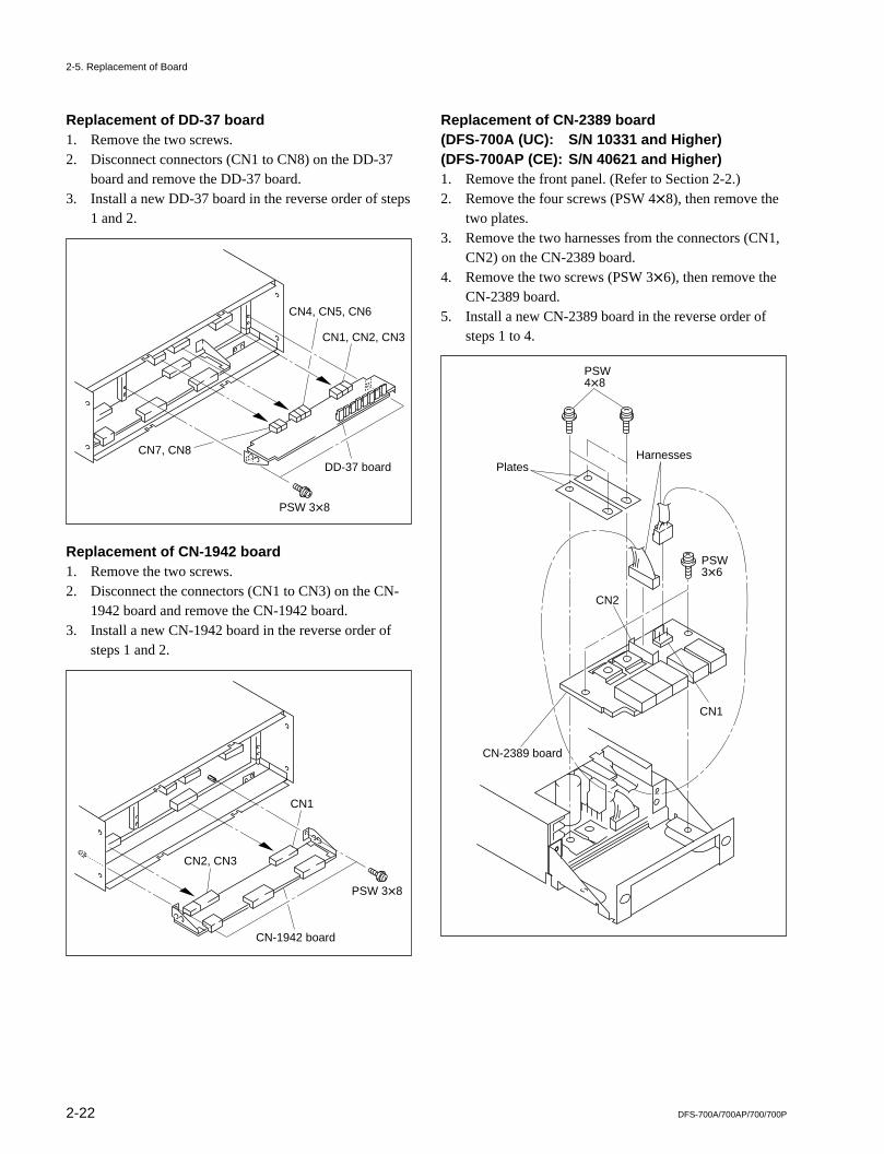
Replacement of DD-37 board1. Remove the two screws.2. Disconnect connectors (CN1 to CN8) on the DD-37
board and remove the DD-37 board.3. Install a new DD-37 board in the reverse order of steps
1 and 2.
Replacement of CN-1942 board1. Remove the two screws.2. Disconnect the connectors (CN1 to CN3) on the CN-
1942 board and remove the CN-1942 board.3. Install a new CN-1942 board in the reverse order of
steps 1 and 2.
PSW 3x8
CN7, CN8
CN4, CN5, CN6
CN1, CN2, CN3
DD-37 board
PSW 3x8
CN1
CN2, CN3
CN-1942 board
2-5. Replacement of Board
Replacement of CN-2389 board(DFS-700A (UC): S/N 10331 and Higher)(DFS-700AP (CE): S/N 40621 and Higher)1. Remove the front panel. (Refer to Section 2-2.)2. Remove the four screws (PSW 4x8), then remove the
two plates.3. Remove the two harnesses from the connectors (CN1,
CN2) on the CN-2389 board.4. Remove the two screws (PSW 3x6), then remove the
CN-2389 board.5. Install a new CN-2389 board in the reverse order of
steps 1 to 4.
Harnesses
CN2
CN1
CN-2389 board
PSW3x6
PSW4x8
Plates
2-23DFS-700A/700AP/700/700P
2-6. Replacement of Switching Regulator
PSW 3x8Handle
Power supply unit
PSW3x8
PSW3x6
Power supply unit bracket
PSW 3x6
Switching regulatorHarnesses
CN-2389 bracket
CN203
CN1
Plates
PSW4x8
2-6. Replacement of Switching Regulator
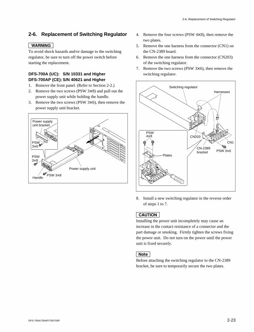
wTo avoid shock hazards and/or damage to the switchingregulator, be sure to turn off the power switch beforestarting the replacement.
DFS-700A (UC): S/N 10331 and HigherDFS-700AP (CE): S/N 40621 and Higher1. Remove the front panel. (Refer to Section 2-2.)2. Remove the two screws (PSW 3x8) and pull out the
power supply unit while holding the handle.3. Remove the two screws (PSW 3x6), then remove the
power supply unit bracket.
4. Remove the four screws (PSW 4x8), then remove thetwo plates.
5. Remove the one harness from the connector (CN1) onthe CN-2389 board.
6. Remove the one harness from the connector (CN203)of the switching regulator.
7. Remove the two screws (PSW 3x6), then remove theswitching regulator.
8. Install a new switching regulator in the reverse orderof steps 1 to 7.
cInstalling the power unit incompletely may cause anincrease in the contact resistance of a connector and thepart damage or smoking. Firmly tighten the screws fixingthe power unit. Do not turn on the power until the powerunit is fixed securely.
nBefore attaching the switching regulator to the CN-2389bracket, be sure to temporarily secure the two plates.
2-24 DFS-700A/700AP/700/700P
DFS-700A (UC): S/N 10001-10330DFS-700AP (CE): S/N 40001-40620DFS-700 (UC): S/N 10001 and HigherDFS-700P (CE): S/N 40001 and Higher1. Remove the front panel. (Refer to Section 2-2.)2. Remove the two screws and pull out the switching
regulator while holding the handle.
3. Install a new switching regulator in the reverse orderof steps 1 and 2.
cInstalling the power unit incompletely may cause anincrease in the contact resistance of a connector and thepart damage or smoking. Firmly tighten the screws fixingthe power unit. Do not turn on the power until the powerunit is fixed securely.
nFor the adjustment after the switching regulatorreplacement, refer to “4-8. Adjusting the Power SupplyVoltage”.
2-6. Replacement of Switching Regulator2-7. Replacement of DC Fan
PSW 3x8
Handle
Switching regulator
PSW3x8
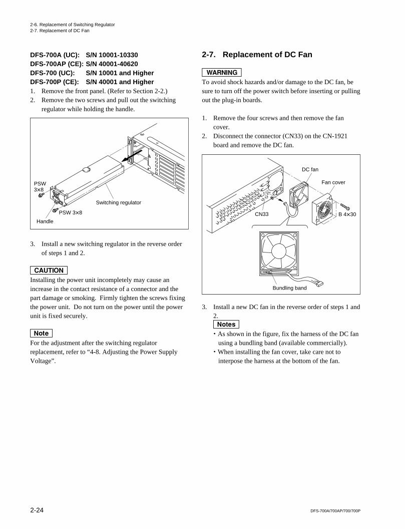
2-7. Replacement of DC Fan
wTo avoid shock hazards and/or damage to the DC fan, besure to turn off the power switch before inserting or pullingout the plug-in boards.
1. Remove the four screws and then remove the fancover.
2. Disconnect the connector (CN33) on the CN-1921board and remove the DC fan.
3. Install a new DC fan in the reverse order of steps 1 and2.m. As shown in the figure, fix the harness of the DC fan using a bundling band (available commercially).. When installing the fan cover, take care not to interpose the harness at the bottom of the fan.
B 4x30
Bundling band
Fan cover
DC fan
CN33
2-25DFS-700A/700AP/700/700P
2-8. Replacement of Main Parts onControl Panel
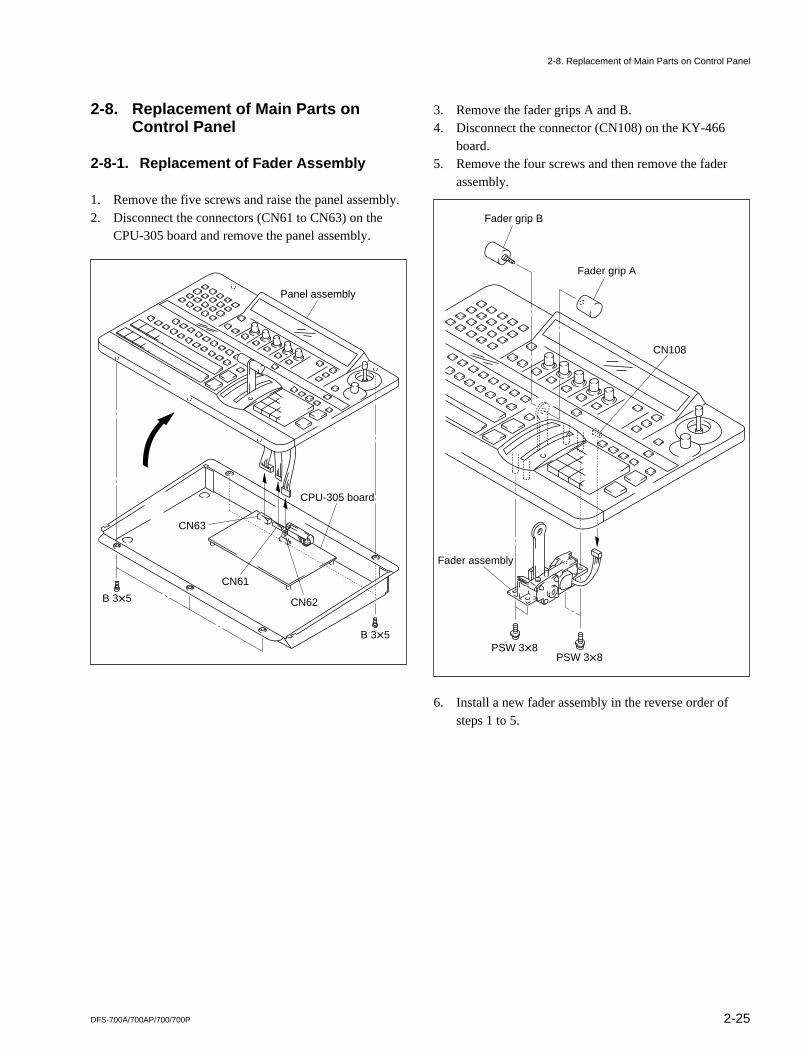
2-8-1. Replacement of Fader Assembly
1. Remove the five screws and raise the panel assembly.2. Disconnect the connectors (CN61 to CN63) on the
CPU-305 board and remove the panel assembly.
B 3x5
B 3x5
CPU-305 board
Panel assembly
CN63
CN61
CN62
2-8. Replacement of Main Parts on Control Panel
3. Remove the fader grips A and B.4. Disconnect the connector (CN108) on the KY-466
board.5. Remove the four screws and then remove the fader
assembly.
6. Install a new fader assembly in the reverse order ofsteps 1 to 5.
Fader assembly
Fader grip B
Fader grip A
CN108
PSW 3x8PSW 3x8
2-26 DFS-700A/700AP/700/700P
Fader assembly Gear
Rotary encoder
B 2x4
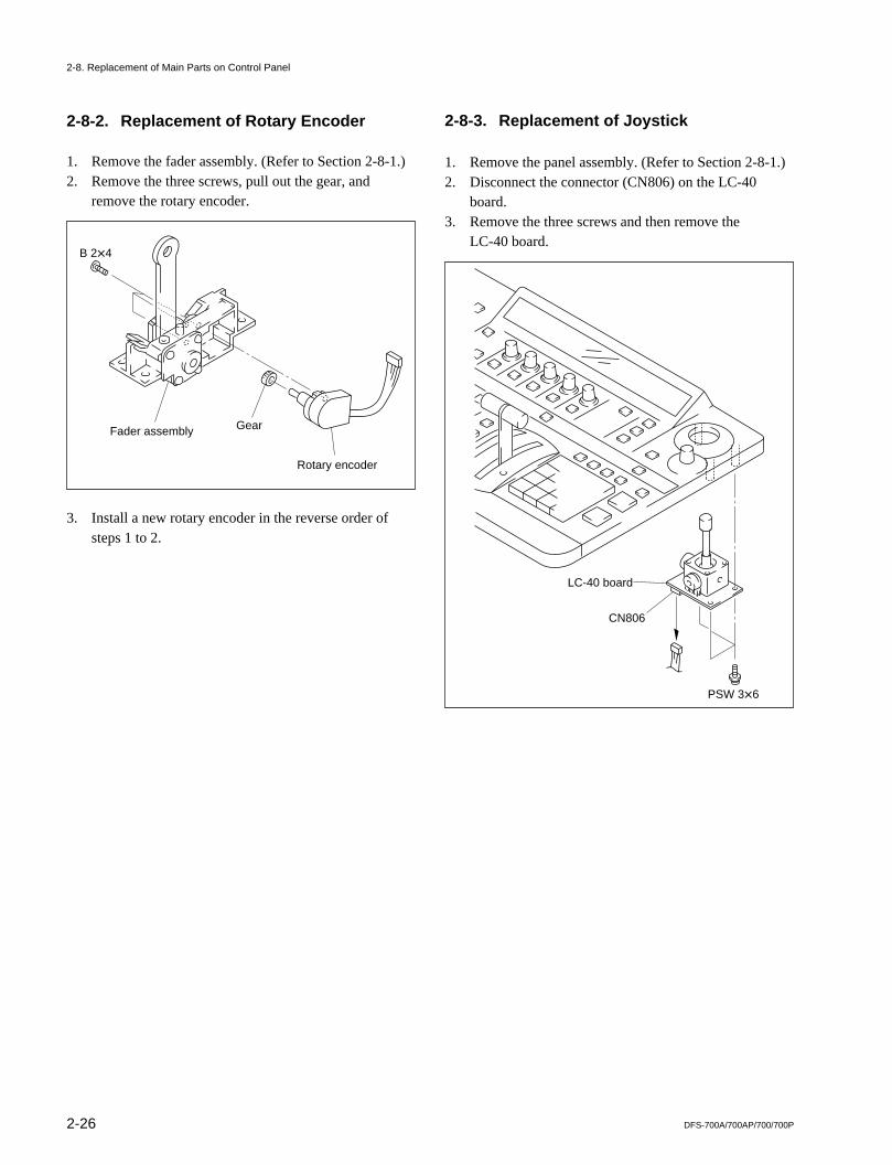
2-8-2. Replacement of Rotary Encoder
1. Remove the fader assembly. (Refer to Section 2-8-1.)2. Remove the three screws, pull out the gear, and
remove the rotary encoder.
3. Install a new rotary encoder in the reverse order ofsteps 1 to 2.
2-8. Replacement of Main Parts on Control Panel
2-8-3. Replacement of Joystick
1. Remove the panel assembly. (Refer to Section 2-8-1.)2. Disconnect the connector (CN806) on the LC-40
board.3. Remove the three screws and then remove the
LC-40 board.
LC-40 board
CN806
PSW 3x6
2-27DFS-700A/700AP/700/700P
Unsolder (at six points).
LC-40 board
Joystick
B 3x8
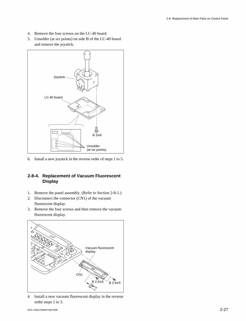
4. Remove the four screws on the LC-40 board.5. Unsolder (at six points) on side B of the LC-40 board
and remove the joystick.
6. Install a new joystick in the reverse order of steps 1 to 5.
2-8-4. Replacement of Vacuum FluorescentDisplay
1. Remove the panel assembly. (Refer to Section 2-8-1.)2. Disconnect the connector (CN1) of the vacuum
fluorescent display.3. Remove the four screws and then remove the vacuum
fluorescent display.
4. Install a new vacuum fluorescent display in the reverseorder steps 1 to 3.
Vacuum fluorescentdisplay
CN1
B 2.6x5B 2.6x5
2-8. Replacement of Main Parts on Control Panel
2-28 DFS-700A/700AP/700/700P
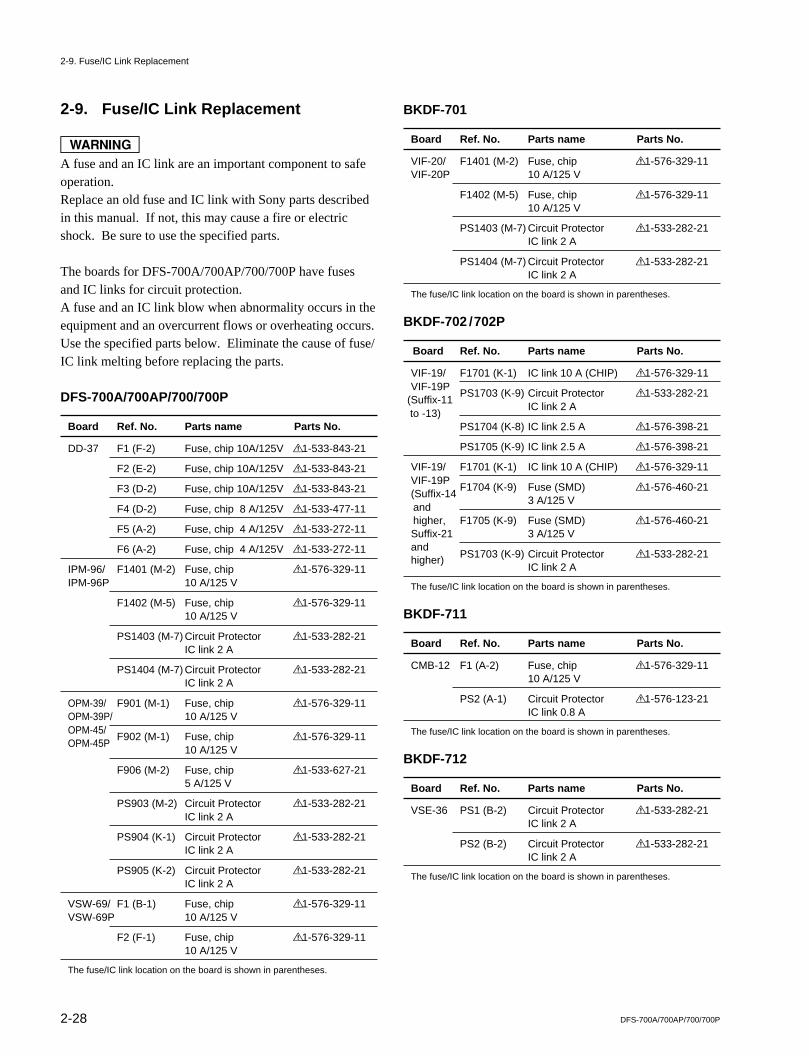
2-9. Fuse/IC Link Replacement
wA fuse and an IC link are an important component to safeoperation.Replace an old fuse and IC link with Sony parts describedin this manual. If not, this may cause a fire or electricshock. Be sure to use the specified parts.
The boards for DFS-700A/700AP/700/700P have fusesand IC links for circuit protection.A fuse and an IC link blow when abnormality occurs in theequipment and an overcurrent flows or overheating occurs.Use the specified parts below. Eliminate the cause of fuse/IC link melting before replacing the parts.
DFS-700A/700AP/700/700P
Board Ref. No. Parts name Parts No.
DD-37 F1 (F-2) Fuse, chip 10A/125V !1-533-843-21
F2 (E-2) Fuse, chip 10A/125V !1-533-843-21
F3 (D-2) Fuse, chip 10A/125V !1-533-843-21
F4 (D-2) Fuse, chip 8 A/125V !1-533-477-11
F5 (A-2) Fuse, chip 4 A/125V !1-533-272-11
F6 (A-2) Fuse, chip 4 A/125V !1-533-272-11
IPM-96/ F1401 (M-2) Fuse, chip !1-576-329-11IPM-96P 10 A/125 V
F1402 (M-5) Fuse, chip !1-576-329-1110 A/125 V
PS1403 (M-7) Circuit Protector !1-533-282-21IC link 2 A
PS1404 (M-7) Circuit Protector !1-533-282-21IC link 2 A
OPM-39/ F901 (M-1) Fuse, chip !1-576-329-11OPM-39P/ 10 A/125 VOPM-45/
F902 (M-1) Fuse, chip !1-576-329-11OPM-45P
10 A/125 V
F906 (M-2) Fuse, chip !1-533-627-215 A/125 V
PS903 (M-2) Circuit Protector !1-533-282-21IC link 2 A
PS904 (K-1) Circuit Protector !1-533-282-21IC link 2 A
PS905 (K-2) Circuit Protector !1-533-282-21IC link 2 A
VSW-69/ F1 (B-1) Fuse, chip !1-576-329-11VSW-69P 10 A/125 V
F2 (F-1) Fuse, chip !1-576-329-1110 A/125 V
The fuse/IC link location on the board is shown in parentheses.
BKDF-701
Board Ref. No. Parts name Parts No.
VIF-20/ F1401 (M-2) Fuse, chip !1-576-329-11VIF-20P 10 A/125 V
F1402 (M-5) Fuse, chip !1-576-329-1110 A/125 V
PS1403 (M-7) Circuit Protector !1-533-282-21IC link 2 A
PS1404 (M-7) Circuit Protector !1-533-282-21IC link 2 A
The fuse/IC link location on the board is shown in parentheses.
BKDF-702 /702P
Board Ref. No. Parts name Parts No.
VIF-19/ F1701 (K-1) IC link 10 A (CHIP) !1-576-329-11VIF-19P
PS1703 (K-9) Circuit Protector !1-533-282-21(Suffix-11
IC link 2 A to -13)
PS1704 (K-8) IC link 2.5 A !1-576-398-21
PS1705 (K-9) IC link 2.5 A !1-576-398-21
VIF-19/ F1701 (K-1) IC link 10 A (CHIP) !1-576-329-11VIF-19P
F1704 (K-9) Fuse (SMD) !1-576-460-21(Suffix-14
3 A/125 V and
F1705 (K-9) Fuse (SMD) !1-576-460-21 higher,3 A/125 VSuffix-21
PS1703 (K-9) Circuit Protector !1-533-282-21and
IC link 2 A
The fuse/IC link location on the board is shown in parentheses.
BKDF-711
Board Ref. No. Parts name Parts No.
CMB-12 F1 (A-2) Fuse, chip !1-576-329-1110 A/125 V
PS2 (A-1) Circuit Protector !1-576-123-21IC link 0.8 A
The fuse/IC link location on the board is shown in parentheses.
BKDF-712
Board Ref. No. Parts name Parts No.
VSE-36 PS1 (B-2) Circuit Protector !1-533-282-21IC link 2 A
PS2 (B-2) Circuit Protector !1-533-282-21IC link 2 A
The fuse/IC link location on the board is shown in parentheses.
2-9. Fuse/IC Link Replacement
higher)
2-29DFS-700A/700AP/700/700P
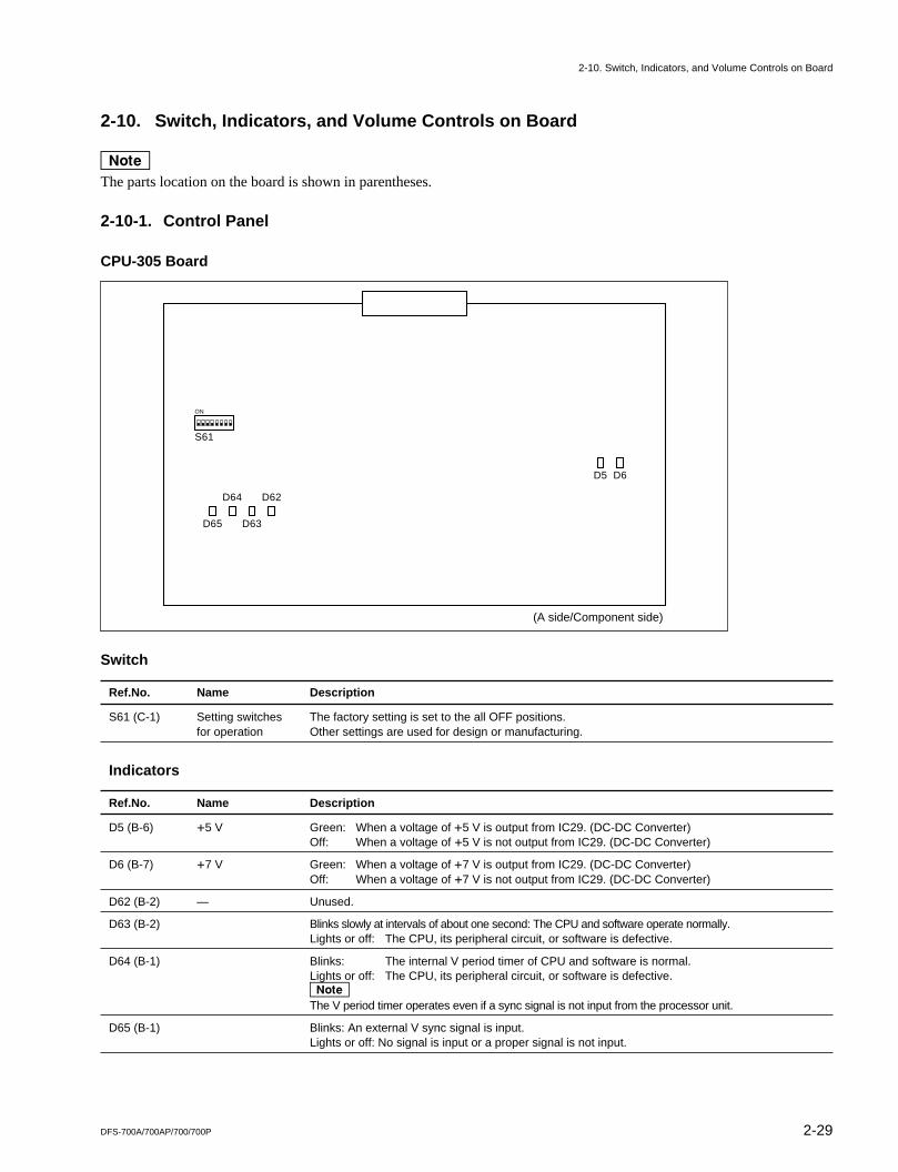
2-10. Switch, Indicators, and Volume Controls on Board
2-10. Switch, Indicators, and Volume Controls on Board
nThe parts location on the board is shown in parentheses.
2-10-1. Control Panel
CPU-305 Board
Switch
Ref.No. Name Description
S61 (C-1) Setting switches The factory setting is set to the all OFF positions.for operation Other settings are used for design or manufacturing.
Indicators
Ref.No. Name Description
D5 (B-6) +5 V Green: When a voltage of +5 V is output from IC29. (DC-DC Converter)Off: When a voltage of +5 V is not output from IC29. (DC-DC Converter)
D6 (B-7) +7 V Green: When a voltage of +7 V is output from IC29. (DC-DC Converter)Off: When a voltage of +7 V is not output from IC29. (DC-DC Converter)
D62 (B-2) — Unused.
D63 (B-2) Blinks slowly at intervals of about one second: The CPU and software operate normally.Lights or off: The CPU, its peripheral circuit, or software is defective.
D64 (B-1) Blinks: The internal V period timer of CPU and software is normal.Lights or off: The CPU, its peripheral circuit, or software is defective.nThe V period timer operates even if a sync signal is not input from the processor unit.
D65 (B-1) Blinks: An external V sync signal is input.Lights or off: No signal is input or a proper signal is not input.
D65
D64
D63
D62
S61
D5 D6
ON
(A side/Component side)
2-30 DFS-700A/700AP/700/700P
S904
RV10021
ONOFF
S901
RV9011
RV8011
RV7051
RV701
RV702
RV706 RV708
RV704
1 RV703
RV704
RV505
11 1
RV501
RV502
1 RV503
RV504
11 1
1 1 1
1
RV305
RV301
RV302
1 RV303
RV304
11 1
1
RV105
RV101
RV102
1 RV103
RV104
11 1
1RV201
1
RV4011
RV6011
ONOFF
S903
RV10011
ONOFF
S902
RV9021
ONOFF
2-10. Switch, Indicators, and Volume Controls on Board
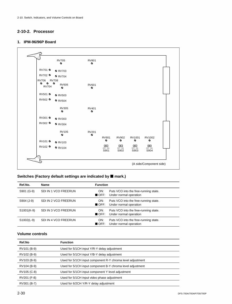
2-10-2. Processor
1. IPM-96/96P Board
Switches (Factory default settings are indicated by \\\\\ mark.)
Ref.No. Name Function
S901 (G-9) SDI IN 1 VCO FREERUN ON: Puts VCO into the free-running state.\ OFF: Under normal operation
S904 (J-9) SDI IN 2 VCO FREERUN ON: Puts VCO into the free-running state.\ OFF: Under normal operation
S1001(K-9) SDI IN 3 VCO FREERUN ON: Puts VCO into the free-running state.\ OFF: Under normal operation
S1002(L-9) SDI IN 4 VCO FREERUN ON: Puts VCO into the free-running state.\ OFF: Under normal operation
Volume controls
Ref.No Function
RV101 (B-9) Used for 5/1CH input Y/R-Y delay adjustment
RV102 (B-9) Used for 5/1CH input Y/B-Y delay adjustment
RV103 (B-9) Used for 5/1CH input component R-Y chroma level adjustment
RV104 (B-9) Used for 5/1CH input component B-Y chroma level adjustment
RV105 (C-8) Used for 5/1CH input component Y level adjustment
RV201 (F-8) Used for 5/1CH input video phase adjustment
RV301 (B-7) Used for 6/2CH Y/R-Y delay adjustment
(A side/Component side)
2-31DFS-700A/700AP/700/700P
2-10. Switch, Indicators, and Volume Controls on Board
Ref.No Function
RV302 (B-7) Used for 6/2CH Y/B-Y delay adjustment
RV303 (B-7) Used for 6/2CH input component R-Y chroma level adjustment
RV304 (B-7) Used for 6/2CH input component B-Y chroma level adjustment
RV305 (C-6) Used for 6/2CH input component Y level adjustment
RV401 (F-6) Used for 6/2CH input video phase adjustment
RV501 (B-4) Used for 7/3CH Y/R-Y delay adjustment
RV502 (B-5) Used for 7/3CH Y/B-Y delay adjustment
RV503 (B-4) Used for 7/3CH input component R-Y chroma level adjustment
RV504 (B-5) Used for 7/3CH input component B-Y chroma level adjustment
RV505 (C-4) Used for 7/3CH input component Y level adjustment
RV601 (F-4) Used for 7/3CH input video phase adjustment
RV701 (B-2) Used for 8/4CH Y/R-Y delay adjustment
RV702 (B-2) Used for 8/4CH Y/B-Y delay adjustment
RV703 (B-2) Used for 8/4CH input component R-Y chroma level adjustment
RV704 (B-2) Used for 8/4CH input component B-Y chroma level adjustment
RV705 (C-1) Used for 8/4CH input component Y level adjustment
RV706 (A-3) RGB input Y level adjustment
RV707 (A-3) RGB input R-Y chroma level adjustment
RV708 (B-3) RGB input B-Y chroma level adjustment
RV801 (F-1) Used for 8/4CH input video phase adjustment
RV901 (G-9) Used for SDI input 1 VCO free-running adjustment
RV902 (J-9) Used for SDI input 2 VCO free-running adjustment
RV1001 (K-9) Used for SDI input 3 VCO free-running adjustment
RV1002 (L-9) Used for SDI input 4 VCO free-running adjustment
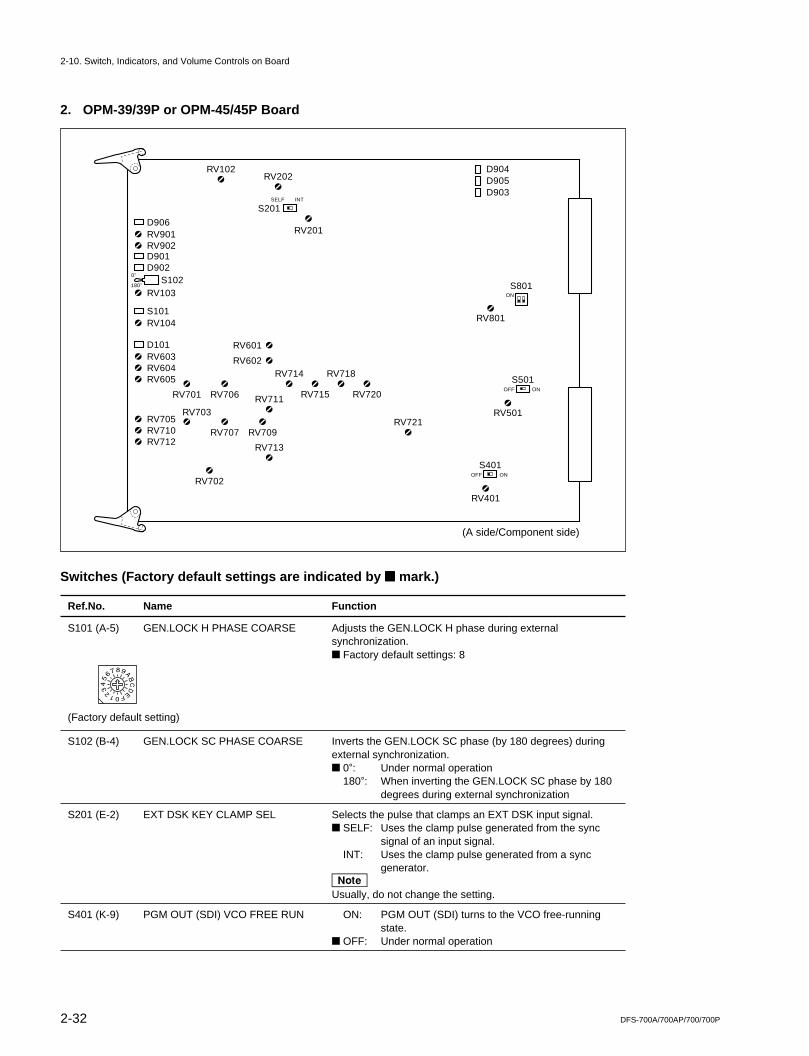
2-32 DFS-700A/700AP/700/700P
S801
RV8011
ON
RV2021
RV1021
RV2011
RV7211
RV7201
RV7181
RV7151
RV7141
RV601 1
RV602 1
RV7111
RV7091
RV7071
RV7021
RV7031
RV7061
RV7011
RV9011RV9021
RV1031
RV7131
S501
RV5011
ON
0d
180d
INTSELF
OFF
S401
RV4011
ONOFF
D906
RV6031RV6041RV6051
RV7051RV7101RV7121
D101
RV1041S101
D901D902
S102
S201
D904D905D903
012345
6789A
BCD
EF
2-10. Switch, Indicators, and Volume Controls on Board
2. OPM-39/39P or OPM-45/45P Board
Switches (Factory default settings are indicated by \\\\\ mark.)
Ref.No. Name Function
S101 (A-5) GEN.LOCK H PHASE COARSE Adjusts the GEN.LOCK H phase during externalsynchronization.\ Factory default settings: 8
(Factory default setting)
S102 (B-4) GEN.LOCK SC PHASE COARSE Inverts the GEN.LOCK SC phase (by 180 degrees) duringexternal synchronization.\ 0d: Under normal operation
180d: When inverting the GEN.LOCK SC phase by 180degrees during external synchronization
S201 (E-2) EXT DSK KEY CLAMP SEL Selects the pulse that clamps an EXT DSK input signal.\ SELF: Uses the clamp pulse generated from the sync
signal of an input signal.INT: Uses the clamp pulse generated from a sync
generator.nUsually, do not change the setting.
S401 (K-9) PGM OUT (SDI) VCO FREE RUN ON: PGM OUT (SDI) turns to the VCO free-runningstate.
\ OFF: Under normal operation
(A side/Component side)
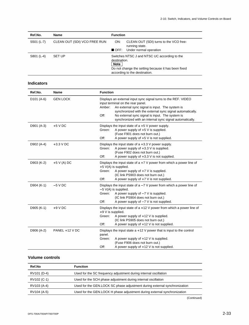
2-33DFS-700A/700AP/700/700P
2-10. Switch, Indicators, and Volume Controls on Board
Ref.No. Name Function
S501 (L-7) CLEAN OUT (SDI) VCO FREE RUN ON: CLEAN OUT (SDI) turns to the VCO free-running state.
\ OFF: Under normal operation
S801 (L-4) SET UP Switches NTSC J and NTSC UC according to thedestination.nDo not change the setting because it has been fixedaccording to the destination.
Indicators
Ref.No. Name Function
D101 (A-6) GEN LOCK Displays an external input sync signal turns to the REF. VIDEOinput terminal on the rear panel.Amber: An external sync signal is input. The system is
synchronized with the external sync signal automatically.Off: No external sync signal is input. The system is
synchronized with an internal sync signal automatically.
D901 (A-3) +5 V DC Displays the input state of a +5 V power supply.Green: A power supply of +5 V is supplied.
(Fuse F901 does not burn out.)Off: A power supply of +5 V is not supplied.
D902 (A-4) +3.3 V DC Displays the input state of a +3.3 V power supply.Green: A power supply of +3.3 V is supplied.
(Fuse F902 does not burn out.)Off: A power supply of +3.3 V is not supplied.
D903 (K-2) +5 V (A) DC Displays the input state of a +7 V power from which a power line of+5 V(A) is supplied.Green: A power supply of +7 V is supplied.
(IC link PS903 does not burn out.)Off: A power supply of +7 V is not supplied.
D904 (K-1) _5 V DC Displays the input state of a _7 V power from which a power line of_5 V(A) is supplied.Green: A power supply of _7 V is supplied.
(IC link PS904 does not burn out.)Off: A power supply of _7 V is not supplied.
D905 (K-1) +9 V DC Displays the input state of a +12 V power from which a power line of+9 V is supplied.Green: A power supply of +12 V is supplied.
(IC link PS905 does not burn out.)Off: A power supply of +12 V is not supplied.
D906 (A-2) PANEL +12 V DC Displays the input state a +12 V power that is input to the controlpanel.Green: A power supply of +12 V is supplied.
(Fuse F906 does not burn out.)Off: A power supply of +12 V is not supplied.
Volume controls
Ref.No Function
RV101 (D-4) Used for the SC frequency adjustment during internal oscillation
RV102 (C-1) Used for the SCH phase adjustment during internal oscillation
RV103 (A-4) Used for the GEN.LOCK SC phase adjustment during external synchronization
RV104 (A-5) Used for the GEN.LOCK H phase adjustment during external synchronization
(Continued)
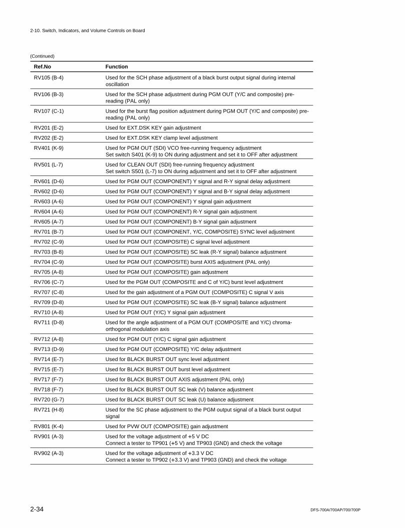
2-34 DFS-700A/700AP/700/700P
2-10. Switch, Indicators, and Volume Controls on Board
(Continued)
Ref.No Function
RV105 (B-4) Used for the SCH phase adjustment of a black burst output signal during internaloscillation
RV106 (B-3) Used for the SCH phase adjustment during PGM OUT (Y/C and composite) pre-reading (PAL only)
RV107 (C-1) Used for the burst flag position adjustment during PGM OUT (Y/C and composite) pre-reading (PAL only)
RV201 (E-2) Used for EXT.DSK KEY gain adjustment
RV202 (E-2) Used for EXT.DSK KEY clamp level adjustment
RV401 (K-9) Used for PGM OUT (SDI) VCO free-running frequency adjustmentSet switch S401 (K-9) to ON during adjustment and set it to OFF after adjustment
RV501 (L-7) Used for CLEAN OUT (SDI) free-running frequency adjustmentSet switch S501 (L-7) to ON during adjustment and set it to OFF after adjustment
RV601 (D-6) Used for PGM OUT (COMPONENT) Y signal and R-Y signal delay adjustment
RV602 (D-6) Used for PGM OUT (COMPONENT) Y signal and B-Y signal delay adjustment
RV603 (A-6) Used for PGM OUT (COMPONENT) Y signal gain adjustment
RV604 (A-6) Used for PGM OUT (COMPONENT) R-Y signal gain adjustment
RV605 (A-7) Used for PGM OUT (COMPONENT) B-Y signal gain adjustment
RV701 (B-7) Used for PGM OUT (COMPONENT, Y/C, COMPOSITE) SYNC level adjustment
RV702 (C-9) Used for PGM OUT (COMPOSITE) C signal level adjustment
RV703 (B-8) Used for PGM OUT (COMPOSITE) SC leak (R-Y signal) balance adjustment
RV704 (C-9) Used for PGM OUT (COMPOSITE) burst AXIS adjustment (PAL only)
RV705 (A-8) Used for PGM OUT (COMPOSITE) gain adjustment
RV706 (C-7) Used for the PGM OUT (COMPOSITE and C of Y/C) burst level adjustment
RV707 (C-8) Used for the gain adjustment of a PGM OUT (COMPOSITE) C signal V axis
RV709 (D-8) Used for PGM OUT (COMPOSITE) SC leak (B-Y signal) balance adjustment
RV710 (A-8) Used for PGM OUT (Y/C) Y signal gain adjustment
RV711 (D-8) Used for the angle adjustment of a PGM OUT (COMPOSITE and Y/C) chroma-orthogonal modulation axis
RV712 (A-8) Used for PGM OUT (Y/C) C signal gain adjustment
RV713 (D-9) Used for PGM OUT (COMPOSITE) Y/C delay adjustment
RV714 (E-7) Used for BLACK BURST OUT sync level adjustment
RV715 (E-7) Used for BLACK BURST OUT burst level adjustment
RV717 (F-7) Used for BLACK BURST OUT AXIS adjustment (PAL only)
RV718 (F-7) Used for BLACK BURST OUT SC leak (V) balance adjustment
RV720 (G-7) Used for BLACK BURST OUT SC leak (U) balance adjustment
RV721 (H-8) Used for the SC phase adjustment to the PGM output signal of a black burst outputsignal
RV801 (K-4) Used for PVW OUT (COMPOSITE) gain adjustment
RV901 (A-3) Used for the voltage adjustment of +5 V DCConnect a tester to TP901 (+5 V) and TP903 (GND) and check the voltage
RV902 (A-3) Used for the voltage adjustment of +3.3 V DCConnect a tester to TP902 (+3.3 V) and TP903 (GND) and check the voltage
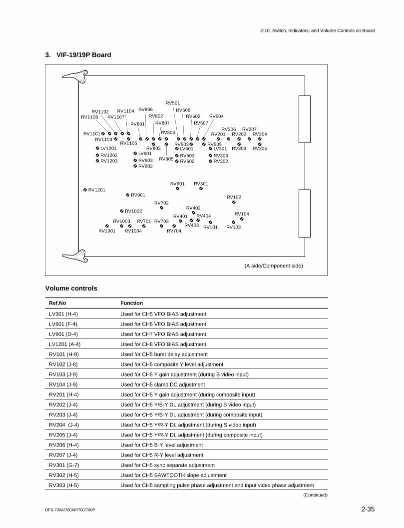
2-35DFS-700A/700AP/700/700P
RV1041
RV1021
RV1031
RV1011
RV4031
RV4041
RV4021
RV4011
RV7041
RV7031
RV7021
RV6011
RV11011
RV1107
1
RV1104
1
RV11051
RV1102
1RV1103 1
RV1106
1
RV801
1
RV807
1RV8041
RV805
1
RV802
1
RV8031
RV806
1
RV501
1
RV507
1
RV504
1RV5051
RV502
1RV5031
RV506
1RV201
1RV204
1
RV207
1RV202
1
RV2051
RV2031
RV206
1
RV3011
RV7011
RV10041
RV10031
RV10011
LV12011RV12021RV12031
RV12011
LV9011RV9031RV9021
LV6011RV6031RV6021
LV3011RV3031RV3021
RV9011
RV10021
2-10. Switch, Indicators, and Volume Controls on Board
3. VIF-19/19P Board
Volume controls
Ref.No Function
LV301 (H-4) Used for CH5 VFO BIAS adjustment
LV601 (F-4) Used for CH6 VFO BIAS adjustment
LV901 (D-4) Used for CH7 VFO BIAS adjustment
LV1201 (A-4) Used for CH8 VFO BIAS adjustment
RV101 (H-9) Used for CH5 burst delay adjustment
RV102 (J-8) Used for CH5 composite Y level adjustment
RV103 (J-9) Used for CH5 Y gain adjustment (during S video input)
RV104 (J-9) Used for CH5 clamp DC adjustment
RV201 (H-4) Used for CH5 Y gain adjustment (during composite input)
RV202 (J-4) Used for CH5 Y/B-Y DL adjustment (during S video input)
RV203 (J-4) Used for CH5 Y/B-Y DL adjustment (during composite input)
RV204 (J-4) Used for CH5 Y/R-Y DL adjustment (during S video input)
RV205 (J-4) Used for CH5 Y/R-Y DL adjustment (during composite input)
RV206 (H-4) Used for CH5 B-Y level adjustment
RV207 (J-4) Used for CH5 R-Y level adjustment
RV301 (G-7) Used for CH5 sync separate adjustment
RV302 (H-5) Used for CH5 SAWTOOTH slope adjustment
RV303 (H-5) Used for CH5 sampling pulse phase adjustment and input video phase adjustment
(Continued)
(A side/Component side)
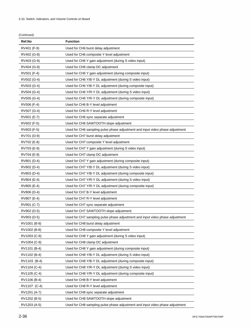
2-36 DFS-700A/700AP/700/700P
2-10. Switch, Indicators, and Volume Controls on Board
(Continued)
Ref.No Function
RV401 (F-9) Used for CH6 burst delay adjustment
RV402 (G-8) Used for CH6 composite Y level adjustment
RV403 (G-9) Used for CH6 Y gain adjustment (during S video input)
RV404 (G-9) Used for CH6 clamp DC adjustment
RV501 (F-4) Used for CH6 Y gain adjustment (during composite input)
RV502 (G-4) Used for CH6 Y/B-Y DL adjustment (during S video input)
RV503 (G-4) Used for CH6 Y/B-Y DL adjustment (during composite input)
RV504 (G-4) Used for CH6 Y/R-Y DL adjustment (during S video input)
RV505 (G-4) Used for CH6 Y/R-Y DL adjustment (during composite input)
RV506 (F-4) Used for CH6 B-Y level adjustment
RV507 (G-4) Used for CH6 R-Y level adjustment
RV601 (E-7) Used for CH6 sync separate adjustment
RV602 (F-5) Used for CH6 SAWTOOTH slope adjustment
RV603 (F-5) Used for CH6 sampling pulse phase adjustment and input video phase adjustment
RV701 (D-9) Used for CH7 burst delay adjustment
RV702 (E-8) Used for CH7 composite Y level adjustment
RV703 (E-9) Used for CH7 Y gain adjustment (during S video input)
RV704 (E-9) Used for CH7 clamp DC adjustment
RV801 (D-4) Used for CH7 Y gain adjustment (during composite input)
RV802 (D-4) Used for CH7 Y/B-Y DL adjustment (during S video input)
RV803 (D-4) Used for CH7 Y/B-Y DL adjustment (during composite input)
RV804 (E-4) Used for CH7 Y/R-Y DL adjustment (during S video input)
RV805 (E-4) Used for CH7 Y/R-Y DL adjustment (during composite input)
RV806 (D-4) Used for CH7 B-Y level adjustment
RV807 (E-4) Used for CH7 R-Y level adjustment
RV901 (C-7) Used for CH7 sync separate adjustment
RV902 (D-5) Used for CH7 SAWTOOTH slope adjustment
RV903 (D-5) Used for CH7 sampling pulse phase adjustment and input video phase adjustment
RV1001 (B-9) Used for CH8 burst delay adjustment
RV1002 (B-8) Used for CH8 composite Y level adjustment
RV1003 (C-9) Used for CH8 Y gain adjustment (during S video input)
RV1004 (C-9) Used for CH8 clamp DC adjustment
RV1101 (B-4) Used for CH8 Y gain adjustment (during composite input)
RV1102 (B-4) Used for CH8 Y/B-Y DL adjustment (during S video input)
RV1103 (B-4) Used for CH8 Y/B-Y DL adjustment (during composite input)
RV1104 (C-4) Used for CH8 Y/R-Y DL adjustment (during S video input)
RV1105 (C-4) Used for CH8 Y/R-Y DL adjustment (during composite input)
RV1106 (B-4) Used for CH8 B-Y level adjustment
RV1107 (C-4) Used for CH8 R-Y level adjustment
RV1201 (A-7) Used for CH8 sync separate adjustment
RV1202 (B-5) Used for CH8 SAWTOOTH slope adjustment
RV1203 (A-5) Used for CH8 sampling pulse phase adjustment and input video phase adjustment
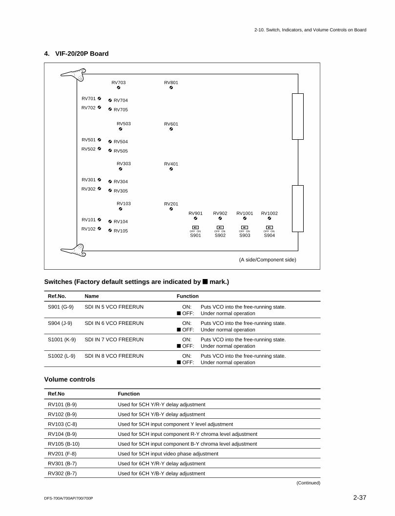
2-37DFS-700A/700AP/700/700P
S904
RV10021
ONOFF
S901
RV9011
RV8011
RV7031
RV701
RV702
1 RV704
RV705
RV503
11 1
RV501
RV502
1 RV504
RV505
11 1
1
RV303
RV301
RV302
1 RV304
RV305
11 1
1
RV103
RV101
RV102
1 RV104
RV105
11 1
1RV201
1
RV4011
RV6011
ONOFF
S903
RV10011
ONOFF
S902
RV9021
ONOFF
2-10. Switch, Indicators, and Volume Controls on Board
4. VIF-20/20P Board
Switches (Factory default settings are indicated by \\\\\ mark.)
Ref.No. Name Function
S901 (G-9) SDI IN 5 VCO FREERUN ON: Puts VCO into the free-running state.\ OFF: Under normal operation
S904 (J-9) SDI IN 6 VCO FREERUN ON: Puts VCO into the free-running state.\ OFF: Under normal operation
S1001 (K-9) SDI IN 7 VCO FREERUN ON: Puts VCO into the free-running state.\ OFF: Under normal operation
S1002 (L-9) SDI IN 8 VCO FREERUN ON: Puts VCO into the free-running state.\ OFF: Under normal operation
Volume controls
Ref.No Function
RV101 (B-9) Used for 5CH Y/R-Y delay adjustment
RV102 (B-9) Used for 5CH Y/B-Y delay adjustment
RV103 (C-8) Used for 5CH input component Y level adjustment
RV104 (B-9) Used for 5CH input component R-Y chroma level adjustment
RV105 (B-10) Used for 5CH input component B-Y chroma level adjustment
RV201 (F-8) Used for 5CH input video phase adjustment
RV301 (B-7) Used for 6CH Y/R-Y delay adjustment
RV302 (B-7) Used for 6CH Y/B-Y delay adjustment
(Continued)
(A side/Component side)
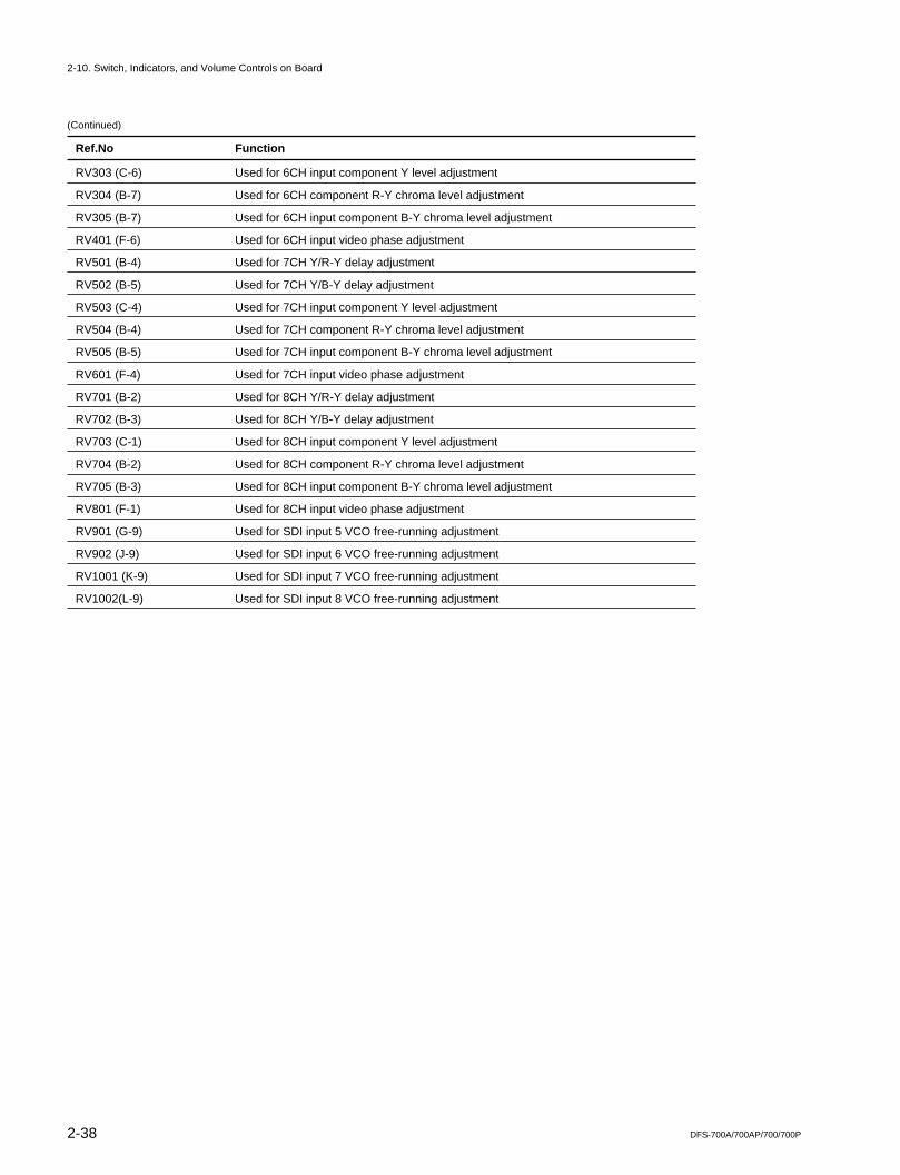
2-38 DFS-700A/700AP/700/700P
2-10. Switch, Indicators, and Volume Controls on Board
(Continued)
Ref.No Function
RV303 (C-6) Used for 6CH input component Y level adjustment
RV304 (B-7) Used for 6CH component R-Y chroma level adjustment
RV305 (B-7) Used for 6CH input component B-Y chroma level adjustment
RV401 (F-6) Used for 6CH input video phase adjustment
RV501 (B-4) Used for 7CH Y/R-Y delay adjustment
RV502 (B-5) Used for 7CH Y/B-Y delay adjustment
RV503 (C-4) Used for 7CH input component Y level adjustment
RV504 (B-4) Used for 7CH component R-Y chroma level adjustment
RV505 (B-5) Used for 7CH input component B-Y chroma level adjustment
RV601 (F-4) Used for 7CH input video phase adjustment
RV701 (B-2) Used for 8CH Y/R-Y delay adjustment
RV702 (B-3) Used for 8CH Y/B-Y delay adjustment
RV703 (C-1) Used for 8CH input component Y level adjustment
RV704 (B-2) Used for 8CH component R-Y chroma level adjustment
RV705 (B-3) Used for 8CH input component B-Y chroma level adjustment
RV801 (F-1) Used for 8CH input video phase adjustment
RV901 (G-9) Used for SDI input 5 VCO free-running adjustment
RV902 (J-9) Used for SDI input 6 VCO free-running adjustment
RV1001 (K-9) Used for SDI input 7 VCO free-running adjustment
RV1002(L-9) Used for SDI input 8 VCO free-running adjustment
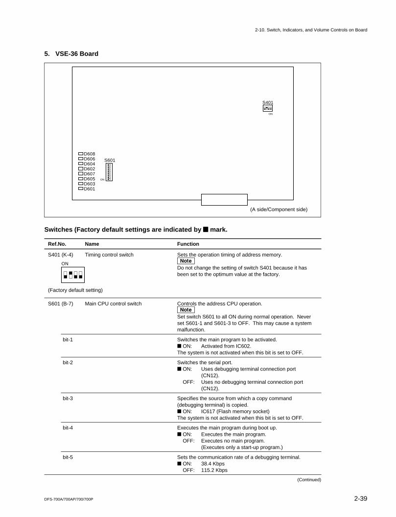
2-39DFS-700A/700AP/700/700P
ON
D607D605D603D601
D604D602
D608D606
S401
S601
ON
ON
2-10. Switch, Indicators, and Volume Controls on Board
5. VSE-36 Board
Switches (Factory default settings are indicated by \\\\\ mark.
Ref.No. Name Function
S401 (K-4) Timing control switch Sets the operation timing of address memory.nDo not change the setting of switch S401 because it hasbeen set to the optimum value at the factory.
(Factory default setting)
S601 (B-7) Main CPU control switch Controls the address CPU operation.nSet switch S601 to all ON during normal operation. Neverset S601-1 and S601-3 to OFF. This may cause a systemmalfunction.
bit-1 Switches the main program to be activated.\ ON: Activated from IC602.The system is not activated when this bit is set to OFF.
bit-2 Switches the serial port.\ ON: Uses debugging terminal connection port
(CN12).OFF: Uses no debugging terminal connection port
(CN12).
bit-3 Specifies the source from which a copy command(debugging terminal) is copied.\ ON: IC617 (Flash memory socket)The system is not activated when this bit is set to OFF.
bit-4 Executes the main program during boot up.\ ON: Executes the main program.
OFF: Executes no main program.(Executes only a start-up program.)
bit-5 Sets the communication rate of a debugging terminal.\ ON: 38.4 Kbps
OFF: 115.2 Kbps
(Continued)
(A side/Component side)
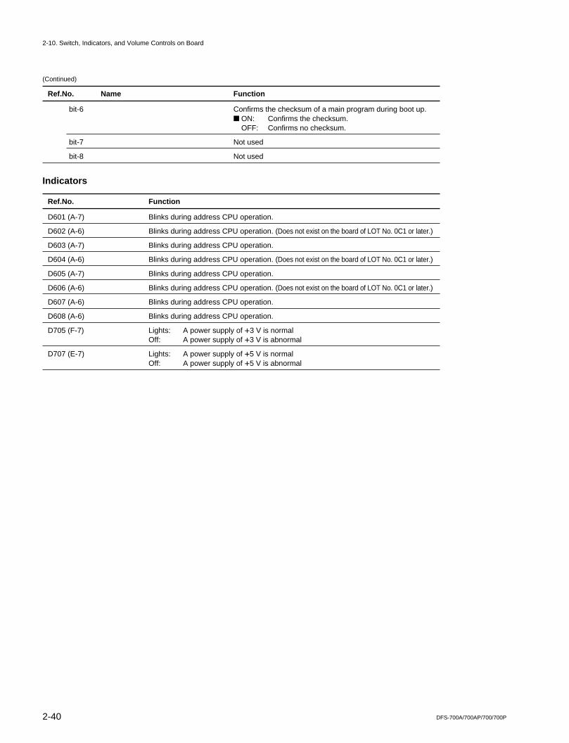
2-40 DFS-700A/700AP/700/700P
2-10. Switch, Indicators, and Volume Controls on Board
(Continued)
Ref.No. Name Function
bit-6 Confirms the checksum of a main program during boot up.\ ON: Confirms the checksum.
OFF: Confirms no checksum.
bit-7 Not used
bit-8 Not used
Indicators
Ref.No. Function
D601 (A-7) Blinks during address CPU operation.
D602 (A-6) Blinks during address CPU operation. (Does not exist on the board of LOT No. 0C1 or later.)
D603 (A-7) Blinks during address CPU operation.
D604 (A-6) Blinks during address CPU operation. (Does not exist on the board of LOT No. 0C1 or later.)
D605 (A-7) Blinks during address CPU operation.
D606 (A-6) Blinks during address CPU operation. (Does not exist on the board of LOT No. 0C1 or later.)
D607 (A-6) Blinks during address CPU operation.
D608 (A-6) Blinks during address CPU operation.
D705 (F-7) Lights: A power supply of +3 V is normalOff: A power supply of +3 V is abnormal
D707 (E-7) Lights: A power supply of +5 V is normalOff: A power supply of +5 V is abnormal
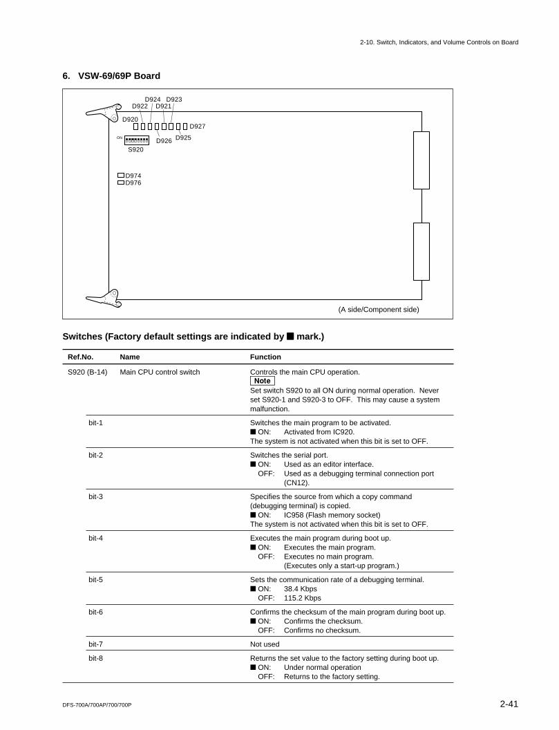
2-41DFS-700A/700AP/700/700P
ON
D920
D926
D927
D924D922
D974D976
S920
D925
D923D921
2-10. Switch, Indicators, and Volume Controls on Board
6. VSW-69/69P Board
Switches (Factory default settings are indicated by \\\\\ mark.)
Ref.No. Name Function
S920 (B-14) Main CPU control switch Controls the main CPU operation.nSet switch S920 to all ON during normal operation. Neverset S920-1 and S920-3 to OFF. This may cause a systemmalfunction.
bit-1 Switches the main program to be activated.\ ON: Activated from IC920.The system is not activated when this bit is set to OFF.
bit-2 Switches the serial port.\ ON: Used as an editor interface.
OFF: Used as a debugging terminal connection port(CN12).
bit-3 Specifies the source from which a copy command(debugging terminal) is copied.\ ON: IC958 (Flash memory socket)The system is not activated when this bit is set to OFF.
bit-4 Executes the main program during boot up.\ ON: Executes the main program.
OFF: Executes no main program.(Executes only a start-up program.)
bit-5 Sets the communication rate of a debugging terminal.\ ON: 38.4 Kbps
OFF: 115.2 Kbps
bit-6 Confirms the checksum of the main program during boot up.\ ON: Confirms the checksum.
OFF: Confirms no checksum.
bit-7 Not used
bit-8 Returns the set value to the factory setting during boot up.\ ON: Under normal operation
OFF: Returns to the factory setting.
(A side/Component side)
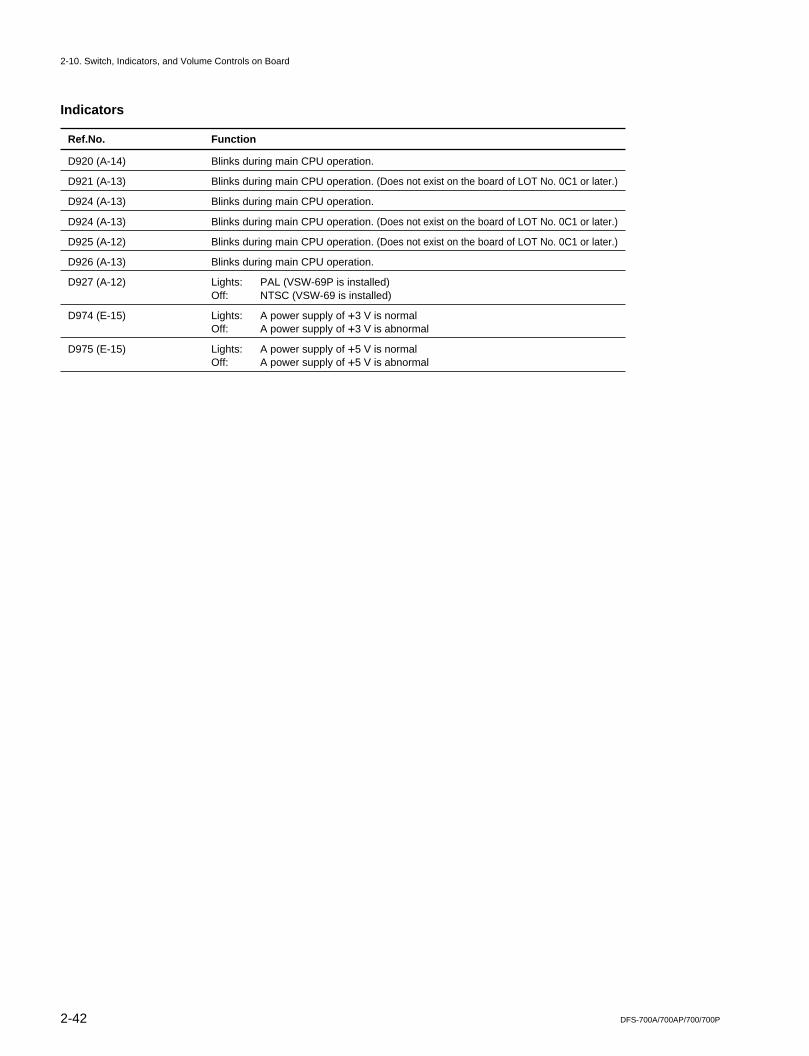
2-42 DFS-700A/700AP/700/700P
Indicators
Ref.No. Function
D920 (A-14) Blinks during main CPU operation.
D921 (A-13) Blinks during main CPU operation. (Does not exist on the board of LOT No. 0C1 or later.)
D924 (A-13) Blinks during main CPU operation.
D924 (A-13) Blinks during main CPU operation. (Does not exist on the board of LOT No. 0C1 or later.)
D925 (A-12) Blinks during main CPU operation. (Does not exist on the board of LOT No. 0C1 or later.)
D926 (A-13) Blinks during main CPU operation.
D927 (A-12) Lights: PAL (VSW-69P is installed)Off: NTSC (VSW-69 is installed)
D974 (E-15) Lights: A power supply of +3 V is normalOff: A power supply of +3 V is abnormal
D975 (E-15) Lights: A power supply of +5 V is normalOff: A power supply of +5 V is abnormal
2-10. Switch, Indicators, and Volume Controls on Board
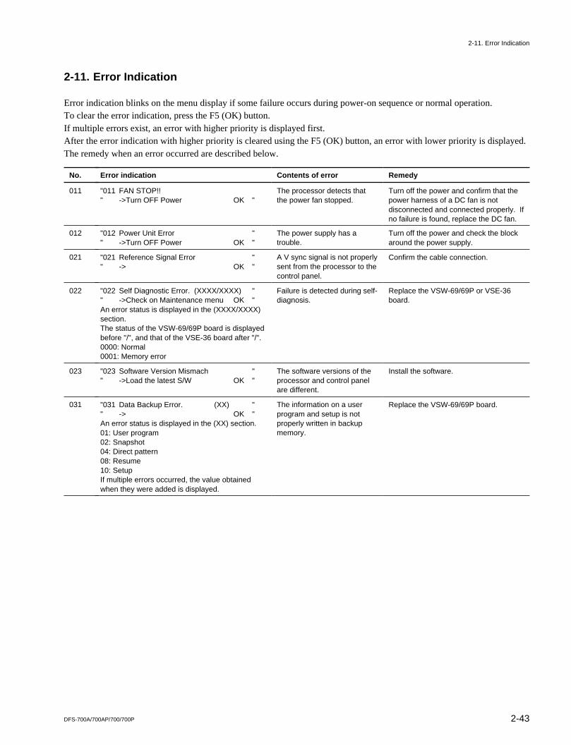
2-43DFS-700A/700AP/700/700P
2-11. Error Indication
2-11. Error Indication
Error indication blinks on the menu display if some failure occurs during power-on sequence or normal operation.To clear the error indication, press the F5 (OK) button.If multiple errors exist, an error with higher priority is displayed first.After the error indication with higher priority is cleared using the F5 (OK) button, an error with lower priority is displayed.The remedy when an error occurred are described below.
Contents of error
The processor detects thatthe power fan stopped.
The power supply has atrouble.
A V sync signal is not properlysent from the processor to thecontrol panel.
Failure is detected during self-diagnosis.
The software versions of theprocessor and control panelare different.
The information on a userprogram and setup is notproperly written in backupmemory.
Remedy
Turn off the power and confirm that thepower harness of a DC fan is notdisconnected and connected properly. Ifno failure is found, replace the DC fan.
Turn off the power and check the blockaround the power supply.
Confirm the cable connection.
Replace the VSW-69/69P or VSE-36board.
Install the software.
Replace the VSW-69/69P board.
Error indication
"011 FAN STOP!!" ->Turn OFF Power OK "
"012 Power Unit Error "" ->Turn OFF Power OK "
"021 Reference Signal Error "" -> OK "
"022 Self Diagnostic Error. (XXXX/XXXX) "" ->Check on Maintenance menu OK "An error status is displayed in the (XXXX/XXXX)section.The status of the VSW-69/69P board is displayedbefore "/", and that of the VSE-36 board after "/".0000: Normal0001: Memory error
"023 Software Version Mismach "" ->Load the latest S/W OK "
"031 Data Backup Error. (XX) "" -> OK "An error status is displayed in the (XX) section.01: User program02: Snapshot04: Direct pattern08: Resume10: SetupIf multiple errors occurred, the value obtainedwhen they were added is displayed.
No.
011
012
021
022
023
031
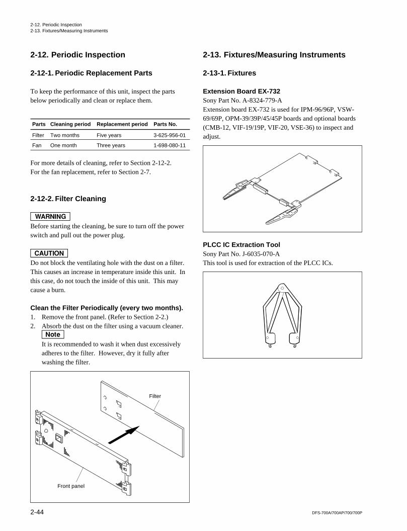
2-44 DFS-700A/700AP/700/700P
2-12. Periodic Inspection
2-12-1. Periodic Replacement Parts
To keep the performance of this unit, inspect the partsbelow periodically and clean or replace them.
Parts Cleaning period Replacement period Parts No.
Filter Two months Five years 3-625-956-01
Fan One month Three years 1-698-080-11
For more details of cleaning, refer to Section 2-12-2.For the fan replacement, refer to Section 2-7.
2-12-2. Filter Cleaning
wBefore starting the cleaning, be sure to turn off the powerswitch and pull out the power plug.
cDo not block the ventilating hole with the dust on a filter.This causes an increase in temperature inside this unit. Inthis case, do not touch the inside of this unit. This maycause a burn.
Clean the Filter Periodically (every two months).1. Remove the front panel. (Refer to Section 2-2.)2. Absorb the dust on the filter using a vacuum cleaner.
nIt is recommended to wash it when dust excessivelyadheres to the filter. However, dry it fully afterwashing the filter.
Front panel
Filter
2-13. Fixtures/Measuring Instruments
2-13-1. Fixtures
Extension Board EX-732Sony Part No. A-8324-779-AExtension board EX-732 is used for IPM-96/96P, VSW-69/69P, OPM-39/39P/45/45P boards and optional boards(CMB-12, VIF-19/19P, VIF-20, VSE-36) to inspect andadjust.
PLCC IC Extraction ToolSony Part No. J-6035-070-AThis tool is used for extraction of the PLCC ICs.
2-12. Periodic Inspection2-13. Fixtures/Measuring Instruments
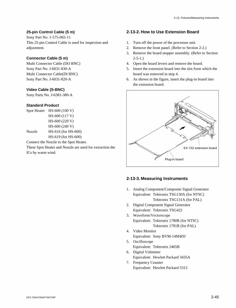
2-45DFS-700A/700AP/700/700P
25-pin Control Cable (5 m)Sony Part No. 1-575-065-11This 25-pin Control Cable is used for inspection andadjustment.
Connector Cable (5 m)Multi Connector Cable (DO BNC)Sony Part No. J-6031-830-AMulti Connector Cable(DI BNC)Sony Part No. J-6031-820-A
Video Cable (S-BNC)Sony Parts No. J-6381-380-A
Standerd ProductSpot Heater HS-600 (100 V)
HS-600 (117 V)HS-600 (220 V)HS-600 (240 V)
Nozzle HS-616 (for HS-600)HS-619 (for HS-600)
Connect the Nozzle to the Spot Heater.These Spot Heater and Nozzle are used for extraction theICs by warm wind.
2-13-2. How to Use Extension Board
1. Turn off the power of the processor unit.2. Remove the front panel. (Refer to Section 2-2.)3. Remove the board stopper assembly. (Refer to Section
2-5-1.)4. Open the board levers and remove the board.5. Insert the extension board into the slot from which the
board was removed in step 4.6. As shown in the figure, insert the plug-in board into
the extension board.
2-13-3. Measuring Instruments
1. Analog Component/Composite Signal GeneratorEquivalent: Tektronix TSG130A (for NTSC)
Tektronix TSG131A (for PAL)2. Digital Component Signal Generator
Equivalent: Tektronix TSG4223. Waveform/Vectorscope
Equivalent: Tektronix 1780R (for NTSC)Tektronix 1781R (for PAL)
4. Video MonitorEquivalent: Sony BVM-14M4DJ
5. OscilloscopeEquivalent: Tektronix 2465B
6. Digital VoltmeterEquivalent: Hewlett Packard 3435A
7. Frequency CounterEquivalent: Hewlett Packard 5313
Plug-in board
EX-732 extension board
2-13. Fixtures/Measuring Instruments

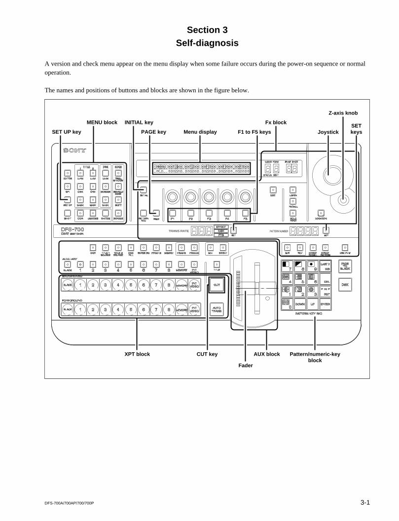
3-1DFS-700A/700AP/700/700P
A version and check menu appear on the menu display when some failure occurs during the power-on sequence or normaloperation.
The names and positions of buttons and blocks are shown in the figure below.
nnnnnnnnnnnnnnnnnnnnnnnnnnnnnnn/m
- unem x x x x xxxx1f 2f xxxxxxxxxxxx 3f 4f 5f
SB-S9950
SB-S9950
SB-S9950
TRANS RATE PATTERN NUMBER
SET UP key
INITIAL key
PAGE key F1 to F5 keysSETkeysMenu display
Fx block
Joystick
Z-axis knob
MENU block
CUT key Pattern/numeric-keyblock
AUX block
Fader
XPT block
Section 3Self-diagnosis
3-2 DFS-700A/700AP/700/700P
3-1. Confirmation of Version
3-1. Confirmation of Version
For the boards (VSW-69, VSE-36, and CPU-305 boards) below, the version of each item can beconfirmed.The version is confirmed on the menu display of the control panel.
Processor
Board Check item Checkpoint on menu display
VSW-69 Main programs (IC920 and IC921) DFS700A or DFS700
Effect data (IC923 and IC924) DATA
VSE-36 Main programs (IC602 to IC605) BKDF712(BKDF-712: Option)
Control Panel
Board Check item Checkpoint on menu display
CPU-305 System control software (IC54) Panel
3-1-1. Execution
1. Press the SET UP key on the MENU block so that page 1/8 of the SET UP menu appears on themenu display.
< Display example >
2. Press the PAGE key on the Fx block to switch the display so that page 2/8 appears on the menudisplay.
< Display example >
3. Press the F2 key to select VER INFORMATION.The version is displayed at the X.XX portion.
< Display example >
SYS SCREEN PPE_RD PORTS TALLY
1/8 4:3 OFF PVE500 OFF
SYS INFO INFO PW ON INSTL
2/8 CONFIG↓ VER↓ FACTRY ↓
INFO DFS700A BKDF712 DATA Panel EXIT
1/1 X.XX X.XX X.XX X.XX ↓
3-3DFS-700A/700AP/700/700P
3-1-2. Viewing the Version
DFS700A: Displays the versions of the main programs (IC920 and IC921) of the VSW-69 board(DFS700) installed in a processor as a standard feature.BKDF712: Displays the versions of the main programs (IC602 to IC605) of the VSE-36 board (BKDF-
712: option) installed in a processor. “0.00” is displayed when BKDF-712 is not installed.DATA: Displays the versions of the effect data (IC923 and IC924) of the VSW-69 board installed in
a processor as a standard feature.Panel: Displays the version of the system control software (IC54) mounted on the CPU-305 board of
the control panel.
3-2. Check Mode
In the check mode, the following items can be confirmed.. Operation of LEDs, switches, joystick, volumes, and fader. Menu display. V sync signal input. Checksum confirmation of system control software on the CPU-305 board
Two types of modes below are available.ALL mode: Used when executing all check items continuously.
However, each check item cannot be selected.PART mode: Used during normal operation.
3-2-1. Activation and Termination
To enter the check mode, switch off the power of the processor.Next, switch on the power of the processor while pressing and holding the following three keyssimultaneously on the control panel; the 0 key at the pattern/numeric-key block, the SET key at theTRANS RATE block (Fx block), and the CUT key at the XPT block. When the check mode isactivated, the top menu appears on the menu display.
< Top menu >
To terminate the check mode, switch off the power of the processor.
3-1. Confirmation of Version3-2. Check Mode
<<< DFS PANEL HARDWARE DIAGNOSES >>>
ALL PART
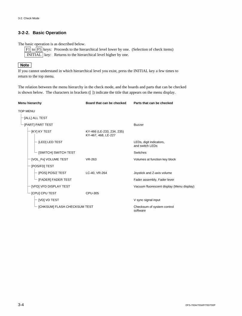
3-4 DFS-700A/700AP/700/700P
3-2. Check Mode
3-2-2. Basic Operation
The basic operation is as described below. F1 to F5 keys: Proceeds to the hierarchical level lower by one. (Selection of check items) INITIAL key: Returns to the hierarchical level higher by one.
nIf you cannot understand in which hierarchical level you exist, press the INITIAL key a few times toreturn to the top menu.
The relation between the menu hierarchy in the check mode, and the boards and parts that can be checkedis shown below. The characters in brackets ([ ]) indicate the title that appears on the menu display.
Menu hierarchy Board that can be checked Parts that can be checked
KY-466 (LE-233, 234, 235)KY-467, 468, LE-227
VR-263
LC-40, VR-264
CPU-305
Buzzer
LEDs, digit indicators, and switch LEDs
Switches
Volumes at function key block
Joystick and Z-axis volume
Fader assembly, Fader lever
Vacuum fluorescent display (Menu display)
V sync signal input
Checksum of system control software
TOP MENU
[ALL] ALL TEST
[PART] PART TEST
[KY] KY TEST
[LED] LED TEST
[SWITCH] SWITCH TEST
[VOL_Fx] VOLUME TEST
[POS/FD] TEST
[POS] POS/Z TEST
[FADER] FADER TEST
[VFD] VFD DISPLAY TEST
[CPU] CPU TEST
[VD] VD TEST
[CHKSUM] FLASH CHECKSUM TEST
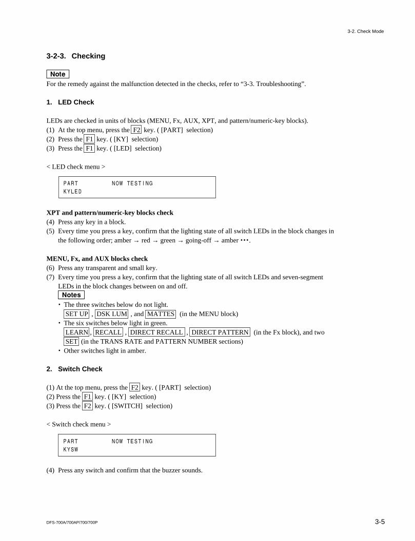
3-5DFS-700A/700AP/700/700P
3-2. Check Mode
3-2-3. Checking
nFor the remedy against the malfunction detected in the checks, refer to “3-3. Troubleshooting”.
1. LED Check
LEDs are checked in units of blocks (MENU, Fx, AUX, XPT, and pattern/numeric-key blocks).(1) At the top menu, press the F2 key. ( [PART] selection)(2) Press the F1 key. ( [KY] selection)(3) Press the F1 key. ( [LED] selection)
< LED check menu >
XPT and pattern/numeric-key blocks check(4) Press any key in a block.(5) Every time you press a key, confirm that the lighting state of all switch LEDs in the block changes in
the following order; amber → red → green → going-off → amber ....
MENU, Fx, and AUX blocks check(6) Press any transparent and small key.(7) Every time you press a key, confirm that the lighting state of all switch LEDs and seven-segment
LEDs in the block changes between on and off.m. The three switches below do not light.
SET UP , DSK LUM , and MATTES (in the MENU block). The six switches below light in green.
LEARN , RECALL , DIRECT RECALL , DIRECT PATTERN (in the Fx block), and two SET (in the TRANS RATE and PATTERN NUMBER sections)
. Other switches light in amber.
2. Switch Check
(1) At the top menu, press the F2 key. ( [PART] selection)(2) Press the F1 key. ( [KY] selection)(3) Press the F2 key. ( [SWITCH] selection)
< Switch check menu >
(4) Press any switch and confirm that the buzzer sounds.
PART NOW TESTING
KYLED
PART NOW TESTING
KYSW
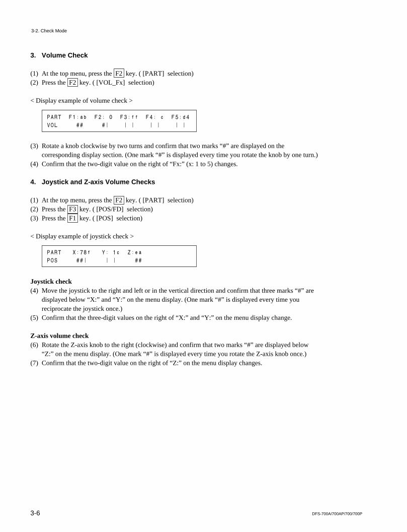
3-6 DFS-700A/700AP/700/700P
3. Volume Check
(1) At the top menu, press the F2 key. ( [PART] selection)(2) Press the F2 key. ( [VOL_Fx] selection)
< Display example of volume check >
(3) Rotate a knob clockwise by two turns and confirm that two marks “#” are displayed on thecorresponding display section. (One mark “#” is displayed every time you rotate the knob by one turn.)
(4) Confirm that the two-digit value on the right of “Fx:” (x: 1 to 5) changes.
4. Joystick and Z-axis Volume Checks
(1) At the top menu, press the F2 key. ( [PART] selection)(2) Press the F3 key. ( [POS/FD] selection)(3) Press the F1 key. ( [POS] selection)
< Display example of joystick check >
Joystick check(4) Move the joystick to the right and left or in the vertical direction and confirm that three marks “#” are
displayed below “X:” and “Y:” on the menu display. (One mark “#” is displayed every time youreciprocate the joystick once.)
(5) Confirm that the three-digit values on the right of “X:” and “Y:” on the menu display change.
Z-axis volume check(6) Rotate the Z-axis knob to the right (clockwise) and confirm that two marks “#” are displayed below
“Z:” on the menu display. (One mark “#” is displayed every time you rotate the Z-axis knob once.)(7) Confirm that the two-digit value on the right of “Z:” on the menu display changes.
PART F1:ab F2: 0 F3:ff F4: c F5:d4
VOL ## #| | | | | | |
PART X:78f Y: 1c Z:ea
POS ##| | | ##
3-2. Check Mode
3-7DFS-700A/700AP/700/700P
5. Fader Check
(1) At the top menu, press the F2 key. ( [PART] selection)(2) Press the F3 key. ( [POS/FD] selection)(3) Press the F2 key. ( [FADER] selection)
< Display example of fader check >
(4) Move the fader from end to end and confirm that four marks “#” are displayed on the correspondingdisplay section. (One mark “#” is displayed every time you reciprocate the fader once.)
(5) Confirm that the three-digit value below “DATA:” on the menu display changes.
6. Menu Display (VFD: Vacuum Fluorescent Display) Check
(1) At the top menu, press the F2 key. ([PART] selection)(2) Press the F4 key. ([VFD] selection)(3) Confirm that all-dot “#” lighting, character “U” display, or character “ ” display is switched every
time you press the F2 key.(4) During all-dot lighting, confirm that no dots are missing.
nIf dots are missing, VFD is judged to be defective.
< Display example of menu display check >
PART DATA TFADER fff 452 ##|
########################################
########################################
UUUUUUUUUUUUUUUUUUUUUUUUUUUUUUUUUUUUUUUU
UUUUUUUUUUUUUUUUUUUUUUUUUUUUUUUUUUUUUUUU
3-2. Check Mode
3-8 DFS-700A/700AP/700/700P
7. V Sync Signal Input Check
(1) At the top menu, press the F2 key. ( [PART] selection)(2) Press the F5 key. ( [CPU] selection)(3) Press the F1 key. ( [VD] selection)
< Display example of V sync signal input check >
(4) During check, confirm that “OK” is displayed on the menu display section “**”.
8. Check of Program Flash Memory (IC54) Checksum
(1) At the top menu, press the F2 key. ([PART] selection)(2) Press the F5 key. ([CPU] selection)(3) Press the F2 key. ([CHKSUM] selection)(4) After the buzzer for calculation completion sounds, confirm that “OK” is displayed on the menu
display.nIt takes a few seconds to calculate the checksum.
< Display example of checksum check >In the case of OK:
In the case of NG:
3-2. Check Mode
PART
CPUVD **
PART
CPUCS OK
PART
CPUCS NG
3-9DFS-700A/700AP/700/700P
3-3.Troubleshooting
3-3. Troubleshooting
The table below shows the possible cause and remedy for the operating situation (malfunction) that occurs in “3-2. Check Mode”.
Checkpoint
LED
Switch
Volume
LED/switch/volume
Joystick
Fader
V sync signalinput
Vacuumfluorescentdisplay (VFD)
Situation
Only one LED does not light.
Multiple LEDs do not light.
All switches (large switches) on theXPT and pattern/numeric-key blocksdo not light.
The buzzer of only one switch doesnot sound.
The buzzer of multiple switchesdoes not sound.
Only one knob does not operate.
Multiple knobs do not operate.
All LEDs, switches, and knobs (notincluding the vacuum fluorescentdisplay) do not operate.
Operation failure
Operation failure
"NG" is displayed on the menudisplay.
“#” is missing during all-dot lighting.
No display
Cause
LED failure
LED failure
IC or the timing signal input to IC isabnormal.
Defective IC29 on the CPU-305board.
Switch failure
Switch failure
IC or the timing signal input to IC isabnormal.
Knob failure
The flexible flat cable between theVR-263 and KY-466 boards is notconnected properly.
Counters (IC208 to IC210, and IC211to IC214: UPG4702G) on the KY-466board are defective.
The flexible flat cable between theVR-263 and KY-466 boards is notconnected properly.
The flat cable between the CPU-305and KY-466 boards is disconnected.
The dual port SRAM (IC64) or dualport memory controller are defective.
Joystick trouble
The harness between the LC-40 andKY-466 boards is disconnected.
The A/D converter (IC215: µ PD7004)on the KY-466 board is defective.
An encoder supplied for the fader isdefective.
The harness connected with the KY-466 board is disconnected.
The counter (IC211: µ PD4701) on theKY-466 board is defective.
RS-422 transceiver (IC24) failure
The cable connected to pin 7 or 20 ofCN21 on the CPU-305 board isdisconnected.
The vacuum fluorescent display isdefective.
The vacuum fluorescent display, IC62,or IC63 is defective, or the harnessconnected with the CPU board isremoved or disconnected.
Remedy
Replace the LED.
Replace the LEDs.
Confirm the connection or replaceIC.
Replace the IC.
Replace the switch.
Replace the switches.
Confirm the connection or replaceIC.
Replace the knob.
Connect the cable.
Replace the counters.
Confirm the cable connection orreplace the cable.
Confirm the cable connection.
Replace the IC.
Replace the joystick.
Confirm the harness connection orreplace the harness.
Replace the A/D converter.
Replace the encoder.
Confirm the harness connection orreplace the harness.
Replace the counter.
Replace the RS-422 transceiver(IC24).
Confirm the connection or replacethe connector.
Replace the vacuum fluorescentdisplay.
Confirm the harness connection orreplace the harness, vacuumfluorescent display, IC62, or IC63.

4-1DFS-700A/700AP/700/700P
4-1. Adjustment Sequence
OPM-39/OPM-45 Board Adjustment (For NTSC)
Section 4Electrical Alignment
4-2. Preparation for Adjustment
4-3-1. +5 V DC Voltage Adjustment
4-3-2. +3.3 V DC Voltage Adjustment
4-3-3. SDI VCO Free-running Frequency Adjustment
4-3-4. PGM OUT Component Y Gain Adjustment
4-3-5. PGM OUT Component R-Y Gain Adjustment
4-3-6. PGM OUT Component B-Y Gain Adjustment
4-3-7. PGM OUT Component Y/C Delay Adjustment
4-3-8. Composite SC Leak Balance Adjustment
4-3-9. Composite Y Gain Adjustment
4-3-10. Composite Modulation AXIS Adjustment
4-3-11. Composite Y/C Delay Adjustment
4-3-12. Composite C Gain Adjustment
4-3-13. Composite Burst Level Adjustment
4-3-14. S VIDEO Y Gain Adjustment
4-3-15. S VIDEO C Gain Adjustment
4-3-16. Black Burst OUT SC Leak Balance Adjustment
4-3-17. Black Burst OUT SC Phase Adjustment
4-3-18. Black Burst OUT SYNC Level Adjustment
4-3-19. Black Burst OUT Burst Level Adjustment
4-3-20. INT SC Frequency Adjustment
4-3-21. INT SCH Phase Adjustment
4-3-22. INT Black Burst OUT SCH Phase Adjustment
4-3-23. GEN Lock H Phase Adjustment
4-3-24. GEN Lock SC Phase Adjustment
4-3-25. PVW OUT Video Gain Adjustment
4-3-26. DSK EXT Key Clamp Level Adjustment
4-3-27. DSK EXT Key Gain Adjustment
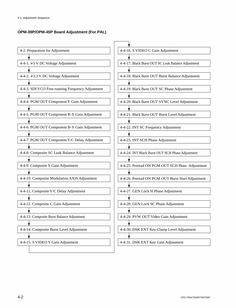
4-2 DFS-700A/700AP/700/700P
4-2. Preparation for Adjustment
4-4-1. +5 V DC Voltage Adjustment
4-4-2. +3.3 V DC Voltage Adjustment
4-4-3. SDI VCO Free-running Frequency Adjustment
4-4-4. PGM OUT Component Y Gain Adjustment
4-4-5. PGM OUT Component R-Y Gain Adjustment
4-4-6. PGM OUT Component B-Y Gain Adjustment
4-4-7. PGM OUT Component Y/C Delay Adjustment
4-4-8. Composite SC Leak Balance Adjustment
4-4-9. Composite Y Gain Adjustment
4-4-10. Composite Modulation AXIS Adjustment
4-4-11. Composite Y/C Delay Adjustment
4-4-12. Composite C Gain Adjustment
4-4-13. Composite Burst Balance Adjustment
4-4-14. Composite Burst Level Adjustment
4-4-15. S VIDEO Y Gain Adjustment
4-4-16. S VIDEO C Gain Adjustment
4-4-17. Black Burst OUT SC Leak Balance Adjustment
4-4-18. Black Burst OUT Burst Balance Adjustment
4-4-19. Black Burst OUT SC Phase Adjustment
4-4-20. Black Burst OUT SYNC Level Adjustment
4-4-21. Black Burst OUT Burst Level Adjustment
4-4-22. INT SC Frequency Adjustment
4-4-23. INT SCH Phase Adjustment
4-4-24. INT Black Burst OUT SCH Phase Adjustment
4-4-25. Preread ON PGM OUT SCH Phase Adjustment
4-4-26. Preread ON PGM OUT Burst Start Adjustment
4-4-27. GEN Lock H Phase Adjustment
4-4-28. GEN Lock SC Phase Adjustment
4-4-29. PVW OUT Video Gain Adjustment
4-4-30. DSK EXT Key Clamp Level Adjustment
4-4-31. DSK EXT Key Gain Adjustment
OPM-39P/OPM-45P Board Adjustment (For PAL)
4-1. Adjustment Sequence
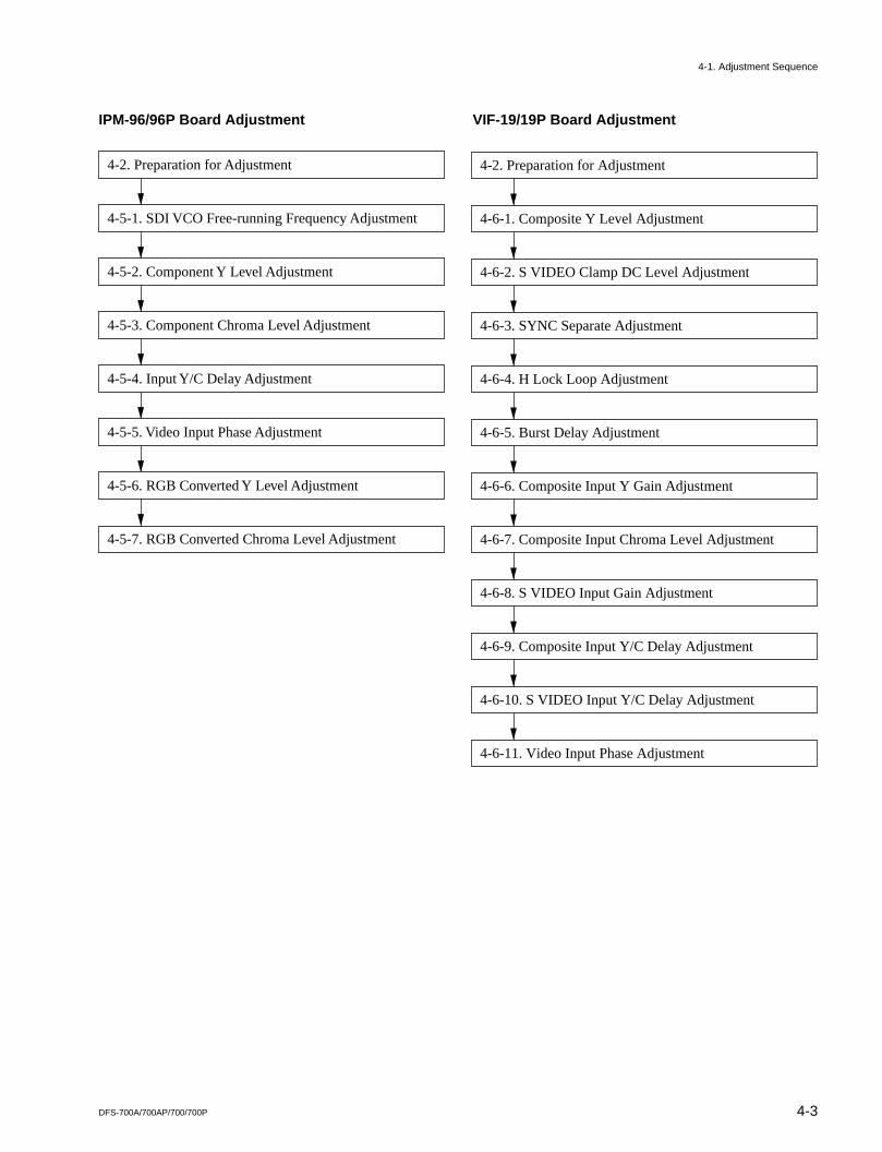
4-3DFS-700A/700AP/700/700P
IPM-96/96P Board Adjustment VIF-19/19P Board Adjustment
4-2. Preparation for Adjustment
4-5-1. SDI VCO Free-running Frequency Adjustment
4-5-2. Component Y Level Adjustment
4-5-3. Component Chroma Level Adjustment
4-5-4. Input Y/C Delay Adjustment
4-5-5. Video Input Phase Adjustment
4-5-6. RGB Converted Y Level Adjustment
4-5-7. RGB Converted Chroma Level Adjustment
4-2. Preparation for Adjustment
4-6-1. Composite Y Level Adjustment
4-6-2. S VIDEO Clamp DC Level Adjustment
4-6-3. SYNC Separate Adjustment
4-6-4. H Lock Loop Adjustment
4-6-5. Burst Delay Adjustment
4-6-6. Composite Input Y Gain Adjustment
4-6-7. Composite Input Chroma Level Adjustment
4-6-8. S VIDEO Input Gain Adjustment
4-6-9. Composite Input Y/C Delay Adjustment
4-6-10. S VIDEO Input Y/C Delay Adjustment
4-6-11. Video Input Phase Adjustment
4-1. Adjustment Sequence
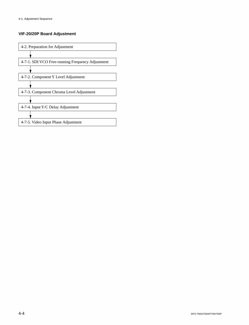
4-4 DFS-700A/700AP/700/700P
VIF-20/20P Board Adjustment
4-2. Preparation for Adjustment
4-7-1. SDI VCO Free-running Frequency Adjustment
4-7-2. Component Y Level Adjustment
4-7-3. Component Chroma Level Adjustment
4-7-4. Input Y/C Delay Adjustment
4-7-5. Video Input Phase Adjustment
4-1. Adjustment Sequence
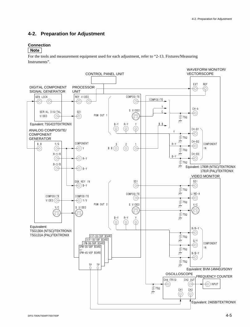
4-5DFS-700A/700AP/700/700P
GEN LOCK
DIGITAL COMPONENTSIGNAL GENERATOR
SERIAL DIGITAL
VIDEO
REF.VIDEO
PROCESSORUNIT
SDI
VIF-20/20P BOARDVIF-19/19P BOARD
IPM-96/96P BOARDOPM-39/39P BOARDorOPM-45/45P BOARD
CONTROL PANEL UNIT
B.B
ANALOG COMPOSITE/COMPONENTGENERATOR
EXT REF
COMPONENT
IN
WAVEFORM MONITOR/VECTORSCOPE
CH-A
CH-B1
CH-B2
CH-B3
Y
B-Y R-Y Y
3
B.B
2 1
SDI
S VIDEO
B.B
C
Y
COMPOSITE
S VIDEO
COMPOSITE
COMPOSITE
R-Y
B-Y
75Z
75Z
75Z
75Z
CH4(TRIG)
OSCILLOSCOPE
Equivalent: 2465B/TEKTRONIX
Equivalent: BVM-14M4DJ/SONY
Equivalent: 1780R (NTSC)/TEKTRONIX 1781R (PAL)/TEKTRONIX
Equivalent: TSG422/TEKTRONIX
Equivalent:TSG130A (NTSC)/TEKTRONIXTSG131A (PAL)/TEKTRONIX
INPUT
FREQUENCY COUNTERCH2 OUT
CH1 CH2
VIDEO MONITOR
LINE-A
Y/C
R/R-Y
G/Y
Y/G
Y/C
COMPOSITE
VIDEO
COMPOSITE
S VIDEO
R-Y/R
B-Y/B
Y
COMPONENT
R-Y
B-Y
B-Y
Y/V
DSK KEY IN
B/B-Y
75Z
75Z
75Z
75Z
75Z
SDI
75Z
COMPONENT
IN
PGM OUT 2
PGM OUT 1
B-Y
TP TP
R-Y Y
75Z
4-2. Preparation for Adjustment
ConnectionnFor the tools and measurement equipment used for each adjustment, refer to “2-13. Fixtures/MeasuringInstruments”.
4-2. Preparation for Adjustment
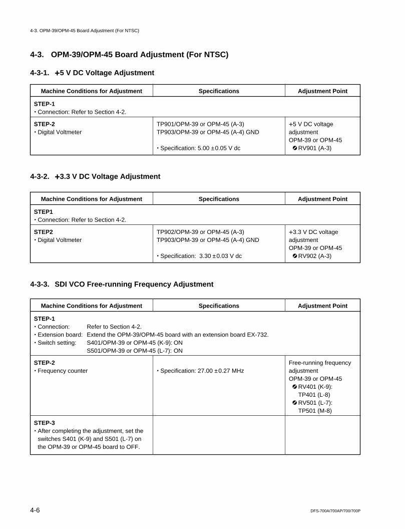
4-6 DFS-700A/700AP/700/700P
Machine Conditions for Adjustment Specifications Adjustment Point
. Specification: 27.00 ±0.27 MHzFree-running frequencyadjustmentOPM-39 or OPM-45
1 RV401 (K-9):TP401 (L-8)
1 RV501 (L-7):TP501 (M-8)
STEP-1. Connection: Refer to Section 4-2.. Extension board: Extend the OPM-39/OPM-45 board with an extension board EX-732.. Switch setting: S401/OPM-39 or OPM-45 (K-9): ON
S501/OPM-39 or OPM-45 (L-7): ON
STEP-2. Frequency counter
STEP-3. After completing the adjustment, set the
switches S401 (K-9) and S501 (L-7) onthe OPM-39 or OPM-45 board to OFF.
4-3-3. SDI VCO Free-running Frequency Adjustment
4-3. OPM-39/OPM-45 Board Adjustment (For NTSC)
4-3-1. +++++5 V DC Voltage Adjustment
Machine Conditions for Adjustment Specifications Adjustment Point
TP901/OPM-39 or OPM-45 (A-3)TP903/OPM-39 or OPM-45 (A-4) GND
. Specification: 5.00 ±0.05 V dc
+5 V DC voltageadjustmentOPM-39 or OPM-45
1 RV901 (A-3)
STEP-1. Connection: Refer to Section 4-2.
STEP-2. Digital Voltmeter
4-3-2. +++++3.3 V DC Voltage Adjustment
Machine Conditions for Adjustment Specifications Adjustment Point
TP902/OPM-39 or OPM-45 (A-3)TP903/OPM-39 or OPM-45 (A-4) GND
. Specification: 3.30 ±0.03 V dc
+3.3 V DC voltageadjustmentOPM-39 or OPM-45
1 RV902 (A-3)
STEP1. Connection: Refer to Section 4-2.
STEP2. Digital Voltmeter
4-3. OPM-39/OPM-45 Board Adjustment (For NTSC)

4-7DFS-700A/700AP/700/700P
4-3. OPM-39/OPM-45 Board Adjustment (For NTSC)
Machine Conditions for Adjustment Specifications Adjustment Point
COMPONENT Y OUT
A = 714 ±5 mV p-pB = 286 ±4 mV p-p
A: Y gain adjustmentOPM-39 or OPM-45
1 RV603 (A-6)
B: SYNC level (Y)OPM-39 or OPM-45
1 RV701 (B-7)
STEP-1. Connection: Refer to Section 4-2.. Extension board: Extend the OPM-39/OPM-45 board with an extension board EX-732.. Test signal: SDI 75 % color bars
STEP-2. (1) or (2) is used.
(1) Waveform MonitorINPUT: CH-AMODE: WAVEFORMREF: EXT
(2) OscilloscopeCH1: 200 mV/DIV
10 us/DIVTRIG: B.B (CH4)
4-3-4. PGM OUT Component Y Gain Adjustment
A
B
Machine Conditions for Adjustment Specifications Adjustment Point
COMPONENT R-Y OUT
A = 700 ±5 mV p-p
R-Y gain adjustmentOPM-39 or OPM-45
1 RV604 (A-6)
STEP-1. Connection: Refer to Section 4-2.. Extension board: Extend the OPM-39/OPM-45 board with an extension board EX-732.. Test signal: SDI 75 % color bars
STEP-2. (1) or (2) Is used.
(1) Waveform MonitorINPUT: CH-B2MODE: WAVEFORMREF: EXT
(2) OscilloscopeCH1: 200 mV/DIV
10 us/DIVTRIG: B.B (CH4)
4-3-5. PGM OUT Component R-Y Gain Adjustment
A
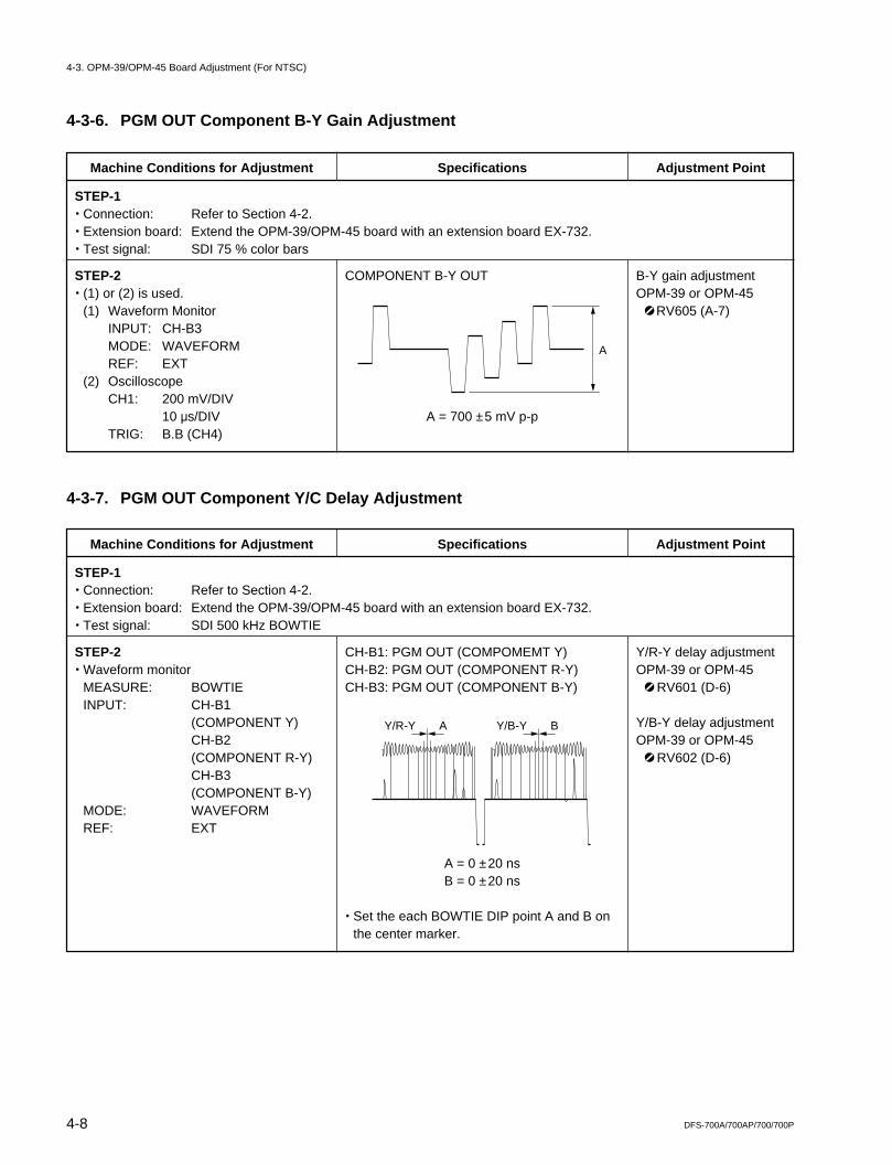
4-8 DFS-700A/700AP/700/700P
Machine Conditions for Adjustment Specifications Adjustment Point
COMPONENT B-Y OUT
A = 700 ±5 mV p-p
B-Y gain adjustmentOPM-39 or OPM-45
1RV605 (A-7)
STEP-1. Connection: Refer to Section 4-2.. Extension board: Extend the OPM-39/OPM-45 board with an extension board EX-732.. Test signal: SDI 75 % color bars
STEP-2. (1) or (2) is used.
(1) Waveform MonitorINPUT: CH-B3MODE: WAVEFORMREF: EXT
(2) OscilloscopeCH1: 200 mV/DIV
10 us/DIVTRIG: B.B (CH4)
4-3-6. PGM OUT Component B-Y Gain Adjustment
A
4-3. OPM-39/OPM-45 Board Adjustment (For NTSC)
Machine Conditions for Adjustment Specifications Adjustment Point
CH-B1: PGM OUT (COMPOMEMT Y)CH-B2: PGM OUT (COMPONENT R-Y)CH-B3: PGM OUT (COMPONENT B-Y)
A = 0 ±20 nsB = 0 ±20 ns
. Set the each BOWTIE DIP point A and B onthe center marker.
Y/R-Y delay adjustmentOPM-39 or OPM-45
1 RV601 (D-6)
Y/B-Y delay adjustmentOPM-39 or OPM-45
1 RV602 (D-6)
STEP-1. Connection: Refer to Section 4-2.. Extension board: Extend the OPM-39/OPM-45 board with an extension board EX-732.. Test signal: SDI 500 kHz BOWTIE
STEP-2. Waveform monitor
MEASURE: BOWTIEINPUT: CH-B1
(COMPONENT Y)CH-B2(COMPONENT R-Y)CH-B3(COMPONENT B-Y)
MODE: WAVEFORMREF: EXT
4-3-7. PGM OUT Component Y/C Delay Adjustment
AY/R-Y BY/B-Y
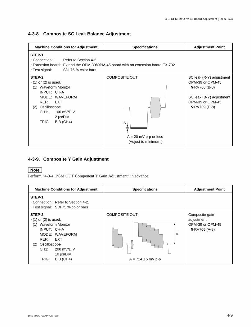
4-9DFS-700A/700AP/700/700P
4-3. OPM-39/OPM-45 Board Adjustment (For NTSC)
Machine Conditions for Adjustment Specifications Adjustment Point
COMPOSITE OUT
A = 20 mV p-p or less (Adjust to minimum.)
SC leak (R-Y) adjustmentOPM-39 or OPM-45
1 RV703 (B-8)
SC leak (B-Y) adjustmentOPM-39 or OPM-45
1 RV709 (D-8)
STEP-1. Connection: Refer to Section 4-2.. Extension board: Extend the OPM-39/OPM-45 board with an extension board EX-732.. Test signal: SDI 75 % color bars
STEP-2. (1) or (2) is used.
(1) Waveform MonitorINPUT: CH-AMODE: WAVEFORMREF: EXT
(2) OscilloscopeCH1: 100 mV/DIV
2 us/DIVTRIG: B.B (CH4)
4-3-8. Composite SC Leak Balance Adjustment
A
Machine Conditions for Adjustment Specifications Adjustment Point
COMPOSITE OUT
A = 714 ±5 mV p-p
Composite gainadjustmentOPM-39 or OPM-45
1 RV705 (A-8)
STEP-1. Connection: Refer to Section 4-2.. Test signal: SDI 75 % color bars
STEP-2. (1) or (2) is used.
(1) Waveform MonitorINPUT: CH-AMODE: WAVEFORMREF: EXT
(2) OscilloscopeCH1: 200 mV/DIV
10 us/DIVTRIG: B.B (CH4)
4-3-9. Composite Y Gain Adjustment
nPerform “4-3-4. PGM OUT Component Y Gain Adjustment” in advance.
A
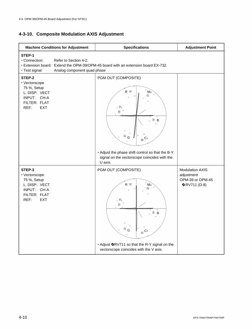
4-10 DFS-700A/700AP/700/700P
Machine Conditions for Adjustment Specifications Adjustment Point
PGM OUT (COMPOSITE)
. Adjust the phase shift control so that the B-Ysignal on the vectorscope coincides with theU axis.
PGM OUT (COMPOSITE)
. Adjust 1RV711 so that the R-Y signal on thevectorscope coincides with the V axis.
Modulation AXISadjustmentOPM-39 or OPM-45
1 RV711 (D-8)
STEP-1. Connection: Refer to Section 4-2.. Extension board: Extend the OPM-39/OPM-45 board with an extension board EX-732.. Test signal: Analog component quad phase
STEP-2. Vectorscope
75 %, SetupL. DISP: VECTINPUT: CH-AFILTER: FLATREF: EXT
STEP-3. Vectorscope
75 %, SetupL. DISP: VECTINPUT: CH-AFILTER: FLATREF: EXT
4-3-10. Composite Modulation AXIS Adjustment
R
G
B
MG
YL
CY
R
G
B
MG
YL
CY
4-3. OPM-39/OPM-45 Board Adjustment (For NTSC)
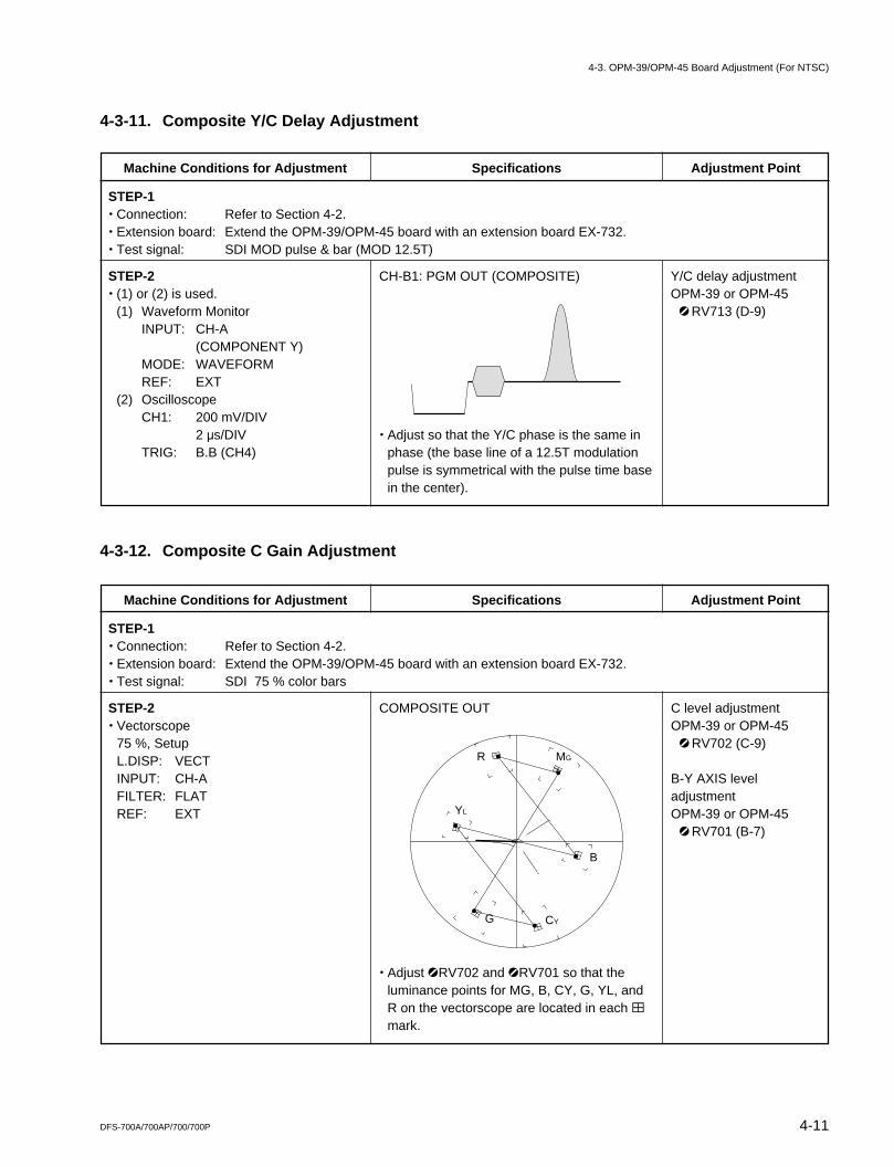
4-11DFS-700A/700AP/700/700P
Adjustment Point
C level adjustmentOPM-39 or OPM-45
1 RV702 (C-9)
B-Y AXIS leveladjustmentOPM-39 or OPM-45
1 RV701 (B-7)
STEP-1. Connection: Refer to Section 4-2.. Extension board: Extend the OPM-39/OPM-45 board with an extension board EX-732.. Test signal: SDI 75 % color bars
4-3-12. Composite C Gain Adjustment
Machine Conditions for Adjustment Specifications Adjustment Point
CH-B1: PGM OUT (COMPOSITE)
. Adjust so that the Y/C phase is the same inphase (the base line of a 12.5T modulationpulse is symmetrical with the pulse time basein the center).
Y/C delay adjustmentOPM-39 or OPM-45
1 RV713 (D-9)
STEP-1. Connection: Refer to Section 4-2.. Extension board: Extend the OPM-39/OPM-45 board with an extension board EX-732.. Test signal: SDI MOD pulse & bar (MOD 12.5T)
STEP-2. (1) or (2) is used.
(1) Waveform MonitorINPUT: CH-A
(COMPONENT Y)MODE: WAVEFORMREF: EXT
(2) OscilloscopeCH1: 200 mV/DIV
2 us/DIVTRIG: B.B (CH4)
4-3-11. Composite Y/C Delay Adjustment
4-3. OPM-39/OPM-45 Board Adjustment (For NTSC)
Machine Conditions for Adjustment Specifications
COMPOSITE OUT
. Adjust 1RV702 and 1RV701 so that theluminance points for MG, B, CY, G, YL, andR on the vectorscope are located in each 4mark.
STEP-2. Vectorscope
75 %, SetupL.DISP: VECTINPUT: CH-AFILTER: FLATREF: EXT
R
G
B
MG
YL
CY
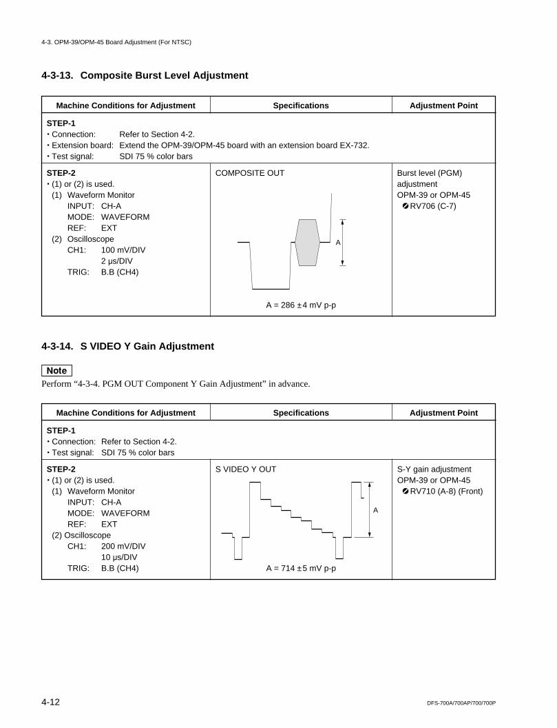
4-12 DFS-700A/700AP/700/700P
Machine Conditions for Adjustment Specifications Adjustment Point
COMPOSITE OUT
A = 286 ±4 mV p-p
Burst level (PGM)adjustmentOPM-39 or OPM-45
1 RV706 (C-7)
STEP-1. Connection: Refer to Section 4-2.. Extension board: Extend the OPM-39/OPM-45 board with an extension board EX-732.. Test signal: SDI 75 % color bars
STEP-2. (1) or (2) is used.
(1) Waveform MonitorINPUT: CH-AMODE: WAVEFORMREF: EXT
(2) OscilloscopeCH1: 100 mV/DIV
2 us/DIVTRIG: B.B (CH4)
4-3-13. Composite Burst Level Adjustment
A
4-3. OPM-39/OPM-45 Board Adjustment (For NTSC)
Machine Conditions for Adjustment Specifications Adjustment Point
S VIDEO Y OUT
A = 714 ±5 mV p-p
S-Y gain adjustmentOPM-39 or OPM-45
1 RV710 (A-8) (Front)
STEP-1. Connection: Refer to Section 4-2.. Test signal: SDI 75 % color bars
STEP-2. (1) or (2) is used.
(1) Waveform MonitorINPUT: CH-AMODE: WAVEFORMREF: EXT
(2) OscilloscopeCH1: 200 mV/DIV
10 us/DIVTRIG: B.B (CH4)
4-3-14. S VIDEO Y Gain Adjustment
nPerform “4-3-4. PGM OUT Component Y Gain Adjustment” in advance.
A
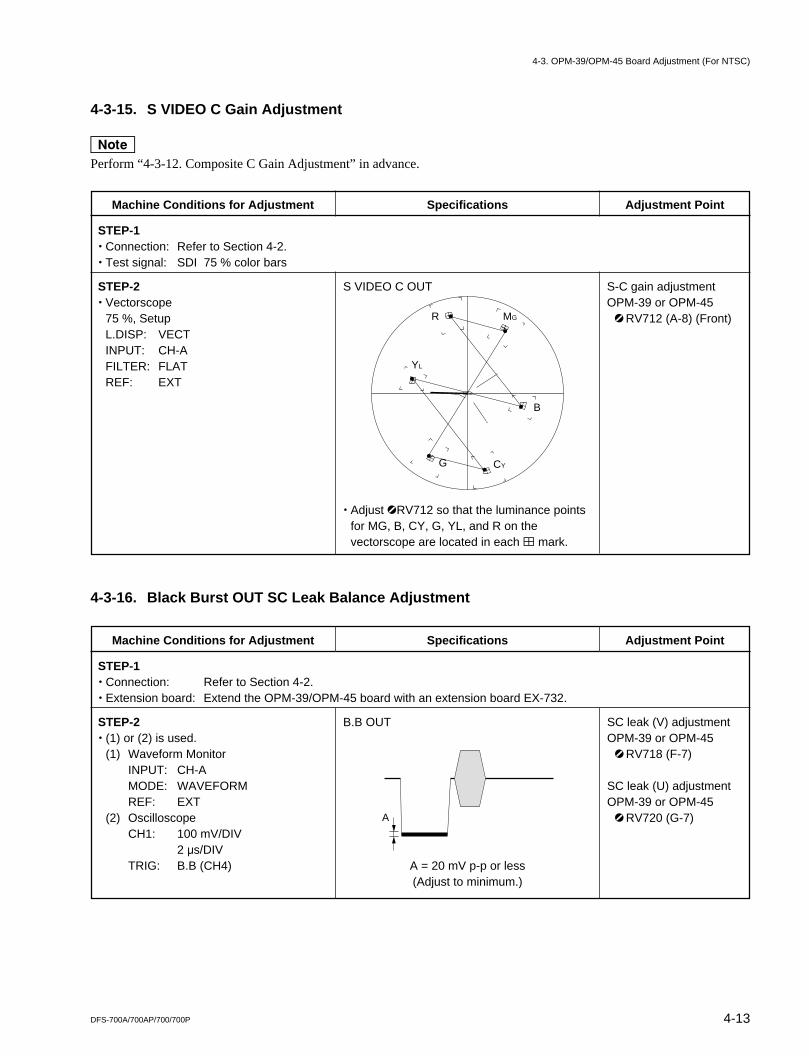
4-13DFS-700A/700AP/700/700P
Machine Conditions for Adjustment Specifications Adjustment Point
B.B OUT
A = 20 mV p-p or less(Adjust to minimum.)
SC leak (V) adjustmentOPM-39 or OPM-45
1 RV718 (F-7)
SC leak (U) adjustmentOPM-39 or OPM-45
1 RV720 (G-7)
STEP-1. Connection: Refer to Section 4-2.. Extension board: Extend the OPM-39/OPM-45 board with an extension board EX-732.
STEP-2. (1) or (2) is used.
(1) Waveform MonitorINPUT: CH-AMODE: WAVEFORMREF: EXT
(2) OscilloscopeCH1: 100 mV/DIV
2 us/DIVTRIG: B.B (CH4)
4-3-16. Black Burst OUT SC Leak Balance Adjustment
A
Machine Conditions for Adjustment Specifications Adjustment Point
S-C gain adjustmentOPM-39 or OPM-45
1 RV712 (A-8) (Front)
STEP-1. Connection: Refer to Section 4-2.. Test signal: SDI 75 % color bars
STEP-2. Vectorscope
75 %, SetupL.DISP: VECTINPUT: CH-AFILTER: FLATREF: EXT
4-3-15. S VIDEO C Gain Adjustment
nPerform “4-3-12. Composite C Gain Adjustment” in advance.
R
G
B
MG
YL
CY
4-3. OPM-39/OPM-45 Board Adjustment (For NTSC)
S VIDEO C OUT
. Adjust 1RV712 so that the luminance pointsfor MG, B, CY, G, YL, and R on thevectorscope are located in each 4 mark.
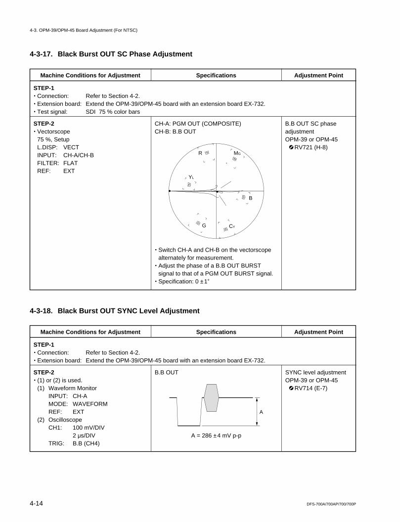
4-14 DFS-700A/700AP/700/700P
Machine Conditions for Adjustment Specifications Adjustment Point
CH-A: PGM OUT (COMPOSITE)CH-B: B.B OUT
. Switch CH-A and CH-B on the vectorscopealternately for measurement.
. Adjust the phase of a B.B OUT BURSTsignal to that of a PGM OUT BURST signal.
. Specification: 0 ±1d
B.B OUT SC phaseadjustmentOPM-39 or OPM-45
1 RV721 (H-8)
STEP-1. Connection: Refer to Section 4-2.. Extension board: Extend the OPM-39/OPM-45 board with an extension board EX-732.. Test signal: SDI 75 % color bars
STEP-2. Vectorscope
75 %, SetupL.DISP: VECTINPUT: CH-A/CH-BFILTER: FLATREF: EXT
4-3-17. Black Burst OUT SC Phase Adjustment
R
G
B
MG
YL
CY
4-3. OPM-39/OPM-45 Board Adjustment (For NTSC)
Machine Conditions for Adjustment Specifications Adjustment Point
B.B OUT
A = 286 ±4 mV p-p
SYNC level adjustmentOPM-39 or OPM-45
1 RV714 (E-7)
STEP-1. Connection: Refer to Section 4-2.. Extension board: Extend the OPM-39/OPM-45 board with an extension board EX-732.
STEP-2. (1) or (2) is used.
(1) Waveform MonitorINPUT: CH-AMODE: WAVEFORMREF: EXT
(2) OscilloscopeCH1: 100 mV/DIV
2 us/DIVTRIG: B.B (CH4)
4-3-18. Black Burst OUT SYNC Level Adjustment
A
4-15DFS-700A/700AP/700/700P
Machine Conditions for Adjustment Specifications Adjustment Point
CH2: TP106/OPM-39 or OPM-45 (D-1)
A = 0.9 ±0.2 V p-p
. Check that the specification above issatisfied.
. Specification: 3,579,545 ±5 Hz
. Check that D101/OPM-39 or OPM-45 (A-6) isoff.
(Check)
SC frequency adjustmentOPM-39 or OPM-45
1 RV101 (D-4)
STEP-1. Connection: Refer to Section 4-2.. Extension board: Extend the OPM-39/OPM-45 board with an extension board EX-732.
STEP-2. Oscilloscope
CH2: 200 mV/DIV (AC)100 ns/DIV
TRIG: CH2
STEP-3. Set the oscilloscope as follows.
CH2: 200 mV/DIV (AC). Connect a frequency counter to CH2
OUT of the oscilloscope.
4-3-20. INT SC Frequency Adjustment
A
Machine Conditions for Adjustment Specifications Adjustment Point
B.B OUT
A = 286 ±4 mV p-p
Burst level adjustmentOPM-39 or OPM-45
1 RV715 (E-7)
STEP-1. Connection: Refer to Section 4-2.. Extension board: Extend the OPM-39/OPM-45 board with an extension board EX-732.
STEP-2. (1) or (2) is used.
(1) Waveform MonitorINPUT: CH-AMODE: WAVEFORMREF: EXT
(2) OscilloscopeCH1: 100 mV/DIV
2 us/DIVTRIG: B.B (CH4)
4-3-19. Black Burst OUT Burst Level Adjustment
A
4-3. OPM-39/OPM-45 Board Adjustment (For NTSC)
4-16 DFS-700A/700AP/700/700P
Machine Conditions for Adjustment Specifications Adjustment Point
PGM OUT (COMPOSITE)
A = 0 ±0.5d
INT SC phaseadjustmentOPM-39 or OPM-45
1RV102 (C-1)
STEP-1. Connection: Refer to Section 4-2.. Extension board: Extend the OPM-39/OPM-45 board with an extension board EX-732.
STEP-2. Vectorscope
75 %, SetupL.DISP: SCHINPUT: CH-AFILTER: FLATGAIN: VARREF: INT
4-3-21. INT SCH Phase Adjustment
A
R
G
B
<NG>
<OK>
MG
YL
CY
R
G
B
MG
YL
CY
4-3. OPM-39/OPM-45 Board Adjustment (For NTSC)
4-17DFS-700A/700AP/700/700P
Machine Conditions for Adjustment Specifications Adjustment Point
B.B OUT
A = 0 ±0.5d
INT B.B OUT SCHphase adjustmentOPM-39 or OPM-45
1 RV105 (B-4)
STEP-1. Connection: Refer to Section 4-2.. Extension board: Extend the OPM-39/OPM-45 board with an extension board EX-732.
STEP-2. Vectorscope
75 %, SetupL.DISP: SCHINPUT: CH-AFILTER: FLATGAIN: VARREF: INT
4-3-22. INT Black Burst OUT SCH Phase Adjustment
A
R
G
B
<NG>
<OK>
MG
YL
CY
R
G
B
MG
YL
CY
4-3. OPM-39/OPM-45 Board Adjustment (For NTSC)
4-18 DFS-700A/700AP/700/700P
Machine Conditions for Adjustment Specifications Adjustment Point
CH1: REF. VIDEOCH2: PGM COMPOSITE (BLACK)
A = 0 ±50 ns
. Check that D101/OPM-39 or OPM-45 (A-6)lights up.
. Adjust 1RV104 (A-5) and S101 (A-5) so thatthe specification above is satisfied.
H phase fine adjustmentOPM-39 or OPM-45
1 RV104 (A-5) (Front)
H phase coarseOPM-39 or OPM-45
S101 (A-5) (Front)
STEP-1. Connection: Refer to Section 4-2.. Connect the REF. VIDEO connector to CH1 of the oscilloscope.. Connect the PGM COMPOSITE connector to CH2 of the oscilloscope and select the BLACK input button.
STEP-2. Oscilloscope
CH1: 200 mV/DIV2 us/DIV
CH2: 200 mV/DIV2 uS/DIV
TRIG: B.B (CH4)
4-3-23. GEN Lock H Phase Adjustment
A
50 %CH1
<NG>
CH2
CH1
<OK>
CH2
50 %
50 %
50 %
4-3. OPM-39/OPM-45 Board Adjustment (For NTSC)
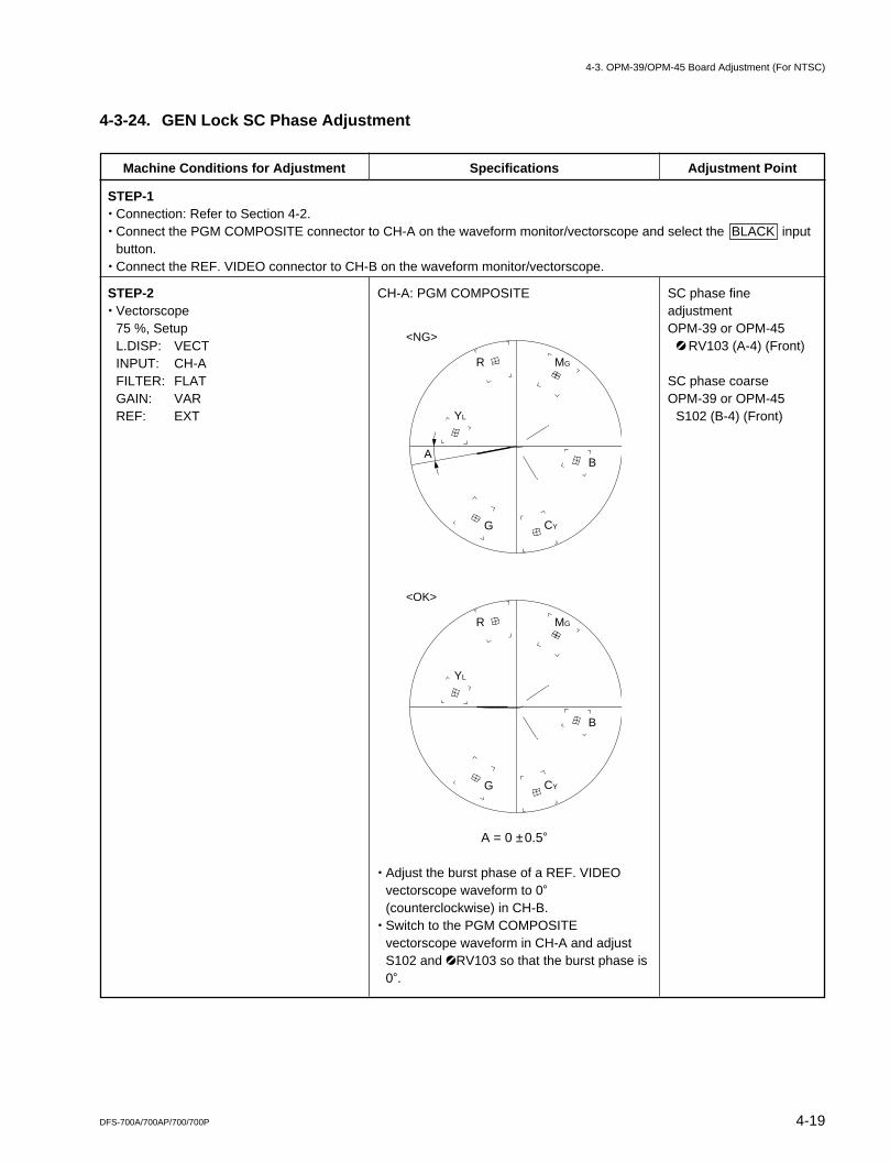
4-19DFS-700A/700AP/700/700P
Machine Conditions for Adjustment Specifications Adjustment Point
CH-A: PGM COMPOSITE
A = 0 ±0.5d
. Adjust the burst phase of a REF. VIDEOvectorscope waveform to 0d(counterclockwise) in CH-B.
. Switch to the PGM COMPOSITEvectorscope waveform in CH-A and adjustS102 and 1RV103 so that the burst phase is0d.
SC phase fineadjustmentOPM-39 or OPM-45
1 RV103 (A-4) (Front)
SC phase coarseOPM-39 or OPM-45
S102 (B-4) (Front)
STEP-1. Connection: Refer to Section 4-2.. Connect the PGM COMPOSITE connector to CH-A on the waveform monitor/vectorscope and select the BLACK input
button.. Connect the REF. VIDEO connector to CH-B on the waveform monitor/vectorscope.
STEP-2. Vectorscope
75 %, SetupL.DISP: VECTINPUT: CH-AFILTER: FLATGAIN: VARREF: EXT
4-3-24. GEN Lock SC Phase Adjustment
A
R
G
B
<NG>
<OK>
MG
YL
CY
R
G
B
MG
YL
CY
4-3. OPM-39/OPM-45 Board Adjustment (For NTSC)
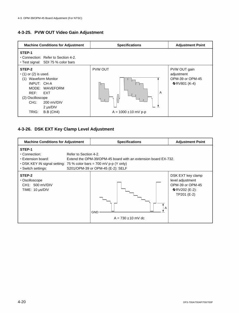
4-20 DFS-700A/700AP/700/700P
Machine Conditions for Adjustment Specifications Adjustment Point
PVW OUT
A = 1000 ±10 mV p-p
PVW OUT gainadjustmentOPM-39 or OPM-45
1 RV801 (K-4)
STEP-1. Connection: Refer to Section 4-2.. Test signal: SDI 75 % color bars
STEP-2. (1) or (2) is used.
(1) Waveform MonitorINPUT: CH-AMODE: WAVEFORMREF: EXT
(2) OscilloscopeCH1: 200 mV/DIV
2 us/DIVTRIG: B.B (CH4)
4-3-25. PVW OUT Video Gain Adjustment
A
4-3. OPM-39/OPM-45 Board Adjustment (For NTSC)
Machine Conditions for Adjustment Specifications Adjustment Point
A = 730 ±10 mV dc
DSK EXT key clamplevel adjustmentOPM-39 or OPM-45
1 RV202 (E-2):TP201 (E-2)
STEP-1. Connection: Refer to Section 4-2.. Extension board: Extend the OPM-39/OPM-45 board with an extension board EX-732.. DSK KEY IN signal setting: 75 % color bars = 700 mV p-p (Y only). Switch settings: S201/OPM-39 or OPM-45 (E-2): SELF
STEP-2. Oscilloscope
CH1: 500 mV/DIVTIME: 10 us/DIV
4-3-26. DSK EXT Key Clamp Level Adjustment
AGND
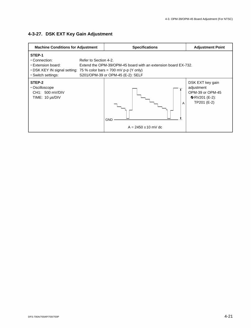
4-21DFS-700A/700AP/700/700P
Machine Conditions for Adjustment Specifications Adjustment Point
A = 2450 ±10 mV dc
DSK EXT key gainadjustmentOPM-39 or OPM-45
1 RV201 (E-2):TP201 (E-2)
STEP-1. Connection: Refer to Section 4-2.. Extension board: Extend the OPM-39/OPM-45 board with an extension board EX-732.. DSK KEY IN signal setting: 75 % color bars = 700 mV p-p (Y only). Switch settings: S201/OPM-39 or OPM-45 (E-2): SELF
STEP-2. Oscilloscope
CH1: 500 mV/DIVTIME: 10 us/DIV
4-3-27. DSK EXT Key Gain Adjustment
A
GND
4-3. OPM-39/OPM-45 Board Adjustment (For NTSC)
4-22 DFS-700A/700AP/700/700P
Machine Conditions for Adjustment Specifications Adjustment Point
. Specification: 27.00 ±0.27 MHzFree-running frequencyadjustmentOPM-39P or OPM-45P
1 RV401 (K-9):TP401 (L-8)
1 RV501 (L-7):TP501 (M-8)
STEP-1. Connection: Refer to Section 4-2.. Extension board: Extend the OPM-39P/OPM-45P board with an extension board EX-732.. Switch setting: S401/OPM-39P or OPM-45P (K-9):ON
S501/OPM-39P or OPM-45P (L-7): ON
STEP-2. Frequency counter
STEP-3. After completing the adjustment, set the
switches S401 (K-9) and S501 (L-7) onthe OPM-39P/OPM-45P board to OFF.
4-4-3. SDI VCO Free-running Frequency Adjustment
4-4. OPM-39P/OPM-45P Board Adjustment (For PAL)
4-4-1. +++++5 V DC Voltage Adjustment
Machine Conditions for Adjustment Specifications Adjustment Point
TP901/OPM-39P or OPM-45P (A-3)TP903/OPM-39P or OPM-45P (A-4) GND
. Specification: 5.00 ±0.05 V dc
+5 V DC voltageadjustmentOPM-39P or OPM-45P
1 RV901 (A-3)
STEP-1. Connection: Refer to Section 4-2.
STEP-2. Digital Voltmeter
4-4-2. +++++3.3 V DC Voltage Adjustment
Machine Conditions for Adjustment Specifications Adjustment Point
TP902/OPM-39P or OPM-45P (A-3)TP903/OPM-39P or OPM-45P (A-4) GND
. Specification: 3.30 ±0.03 V dc
+3.3 V DC voltageadjustmentOPM-39P or OPM-45P
1 RV902 (A-3)
STEP1. Connection: Refer to Section 4-2.
STEP2. Digital Voltmeter
4-4. OPM-39P/OPM-45P Board Adjustment (For PAL)
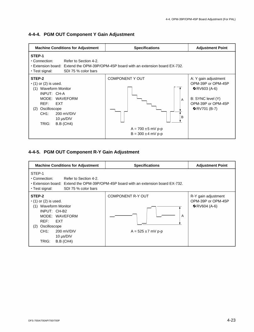
4-23DFS-700A/700AP/700/700P
4-4-4. PGM OUT Component Y Gain Adjustment
Machine Conditions for Adjustment Specifications Adjustment Point
COMPONENT Y OUT
A = 700 ±5 mV p-pB = 300 ±4 mV p-p
A: Y gain adjustmentOPM-39P or OPM-45P
1 RV603 (A-6)
B: SYNC level (Y)OPM-39P or OPM-45P
1 RV701 (B-7)
STEP-1. Connection: Refer to Section 4-2.. Extension board: Extend the OPM-39P/OPM-45P board with an extension board EX-732.. Test signal: SDI 75 % color bars
STEP-2. (1) or (2) is used.
(1) Waveform MonitorINPUT: CH-AMODE: WAVEFORMREF: EXT
(2) OscilloscopeCH1: 200 mV/DIV
10 us/DIVTRIG: B.B (CH4)
A
B
4-4. OPM-39P/OPM-45P Board Adjustment (For PAL)
4-4-5. PGM OUT Component R-Y Gain Adjustment
Machine Conditions for Adjustment Specifications Adjustment Point
COMPONENT R-Y OUT
A = 525 ±7 mV p-p
R-Y gain adjustmentOPM-39P or OPM-45P
1 RV604 (A-6)
STEP-1. Connection: Refer to Section 4-2.. Extension board: Extend the OPM-39P/OPM-45P board with an extension board EX-732.. Test signal: SDI 75 % color bars
STEP-2. (1) or (2) is used.
(1) Waveform MonitorINPUT: CH-B2MODE: WAVEFORMREF: EXT
(2) OscilloscopeCH1: 200 mV/DIV
10 us/DIVTRIG: B.B (CH4)
A

4-24 DFS-700A/700AP/700/700P
Machine Conditions for Adjustment Specifications Adjustment Point
CH-B1: PGM OUT (COMPOMEMT Y)CH-B2: PGM OUT (COMPONENT R-Y)CH-B3: PGM OUT (COMPONENT B-Y)
A = 0 ±20 nsB = 0 ±20 ns
. Set the each BOWTIE DIP point A and B onthe center marker.
Y/R-Y delay adjustmentOPM-39P or OPM-45P
1 RV601 (D-6)
Y/B-Y delay adjustmentOPM-39P or OPM-45P
1 RV602 (D-6)
STEP-1. Connection: Refer to Section 4-2.. Extension board: Extend the OPM-39P/OPM-45P board with an extension board EX-732.. Test signal: SDI 500 kHz BOWTIE
STEP-2. Waveform monitor
MEASURE: BOWTIEINPUT: CH-B1
(COMPONENT Y)CH-B2(COMPONENT R-Y)CH-B3(COMPONENT B-Y)
MODE: WAVEFORMREF: EXT
4-4-7. PGM OUT Component Y/C Delay Adjustment
AY/R-Y BY/B-Y
4-4-6. PGM OUT Component B-Y Gain Adjustment
Machine Conditions for Adjustment Specifications Adjustment Point
COMPONENT B-Y OUT
A = 525 ±7 mV p-p
B-Y gain adjustmentOPM-39P or OPM-45P
1 RV605 (A-7)
STEP-1. Connection: Refer to Section 4-2.. Extension board: Extend the OPM-39P/OPM-45P board with an extension board EX-732.. Test signal: SDI 75 % color bars
STEP-2. (1) or (2) is used.
(1) Waveform MonitorINPUT: CH-B3MODE: WAVEFORMREF: EXT
(2) OscilloscopeCH1: 200 mV/DIV
10 us/DIVTRIG: B.B (CH4)
A
4-4. OPM-39P/OPM-45P Board Adjustment (For PAL)
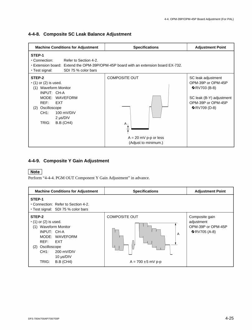
4-25DFS-700A/700AP/700/700P
4-4-8. Composite SC Leak Balance Adjustment
Machine Conditions for Adjustment Specifications Adjustment Point
COMPOSITE OUT
A = 20 mV p-p or less(Adjust to minimum.)
SC leak adjustmentOPM-39P or OPM-45P
1 RV703 (B-8)
SC leak (B-Y) adjustmentOPM-39P or OPM-45P
1 RV709 (D-8)
STEP-1. Connection: Refer to Section 4-2.. Extension board: Extend the OPM-39P/OPM-45P board with an extension board EX-732.. Test signal: SDI 75 % color bars
STEP-2. (1) or (2) is used.
(1) Waveform MonitorINPUT: CH-AMODE: WAVEFORMREF: EXT
(2) OscilloscopeCH1: 100 mV/DIV
2 us/DIVTRIG: B.B (CH4) A
4-4. OPM-39P/OPM-45P Board Adjustment (For PAL)
4-4-9. Composite Y Gain Adjustment
nPerform “4-4-4. PGM OUT Component Y Gain Adjustment” in advance.
Machine Conditions for Adjustment Specifications Adjustment Point
COMPOSITE OUT
A = 700 ±5 mV p-p
Composite gainadjustmentOPM-39P or OPM-45P
1 RV705 (A-8)
STEP-1. Connection: Refer to Section 4-2.. Test signal: SDI 75 % color bars
STEP-2. (1) or (2) is used.
(1) Waveform MonitorINPUT: CH-AMODE: WAVEFORMREF: EXT
(2) OscilloscopeCH1: 200 mV/DIV
10 us/DIVTRIG: B.B (CH4)
A

4-26 DFS-700A/700AP/700/700P
Machine Conditions for Adjustment Specifications Adjustment Point
PGM OUT (COMPOSITE)
. Adjust the phase shift control so that the B-Ysignal on the vectorscope coincides with theU axis.
PGM OUT (COMPOSITE)
. Adjust 1RV711 so that the R-Y signal on thevectorscope coincides with the V axis.
Modulation AXISadjustmentOPM-39P or OPM-45P
1 RV711 (D-8)
STEP-1. Connection: Refer to Section 4-2.. Extension board: Extend the OPM-39P/OPM-45P board with an extension board EX-732.. Test signal: Analog component quad phase
STEP-2. Vectorscope
75 %L. DISP: VECTINPUT: CH-AFILTER: FLATREF: EXT
STEP-3. Vectorscope
75 %L. DISP: VECTINPUT: CH-AFILTER: FLATREF: EXT
R
g
G
r
B
b
MGcy
YL
yl
CY mg
R
g
G
r
B
b
MGcy
YL
yl
CY mg
4-4-10. Composite Modulation AXIS Adjustment
4-4. OPM-39P/OPM-45P Board Adjustment (For PAL)
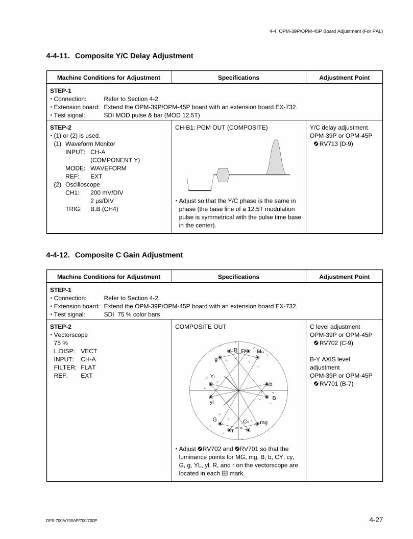
4-27DFS-700A/700AP/700/700P
4-4-11. Composite Y/C Delay Adjustment
Machine Conditions for Adjustment Specifications Adjustment Point
CH-B1: PGM OUT (COMPOSITE)
. Adjust so that the Y/C phase is the same inphase (the base line of a 12.5T modulationpulse is symmetrical with the pulse time basein the center).
Y/C delay adjustmentOPM-39P or OPM-45P
1 RV713 (D-9)
STEP-1. Connection: Refer to Section 4-2.. Extension board: Extend the OPM-39P/OPM-45P board with an extension board EX-732.. Test signal: SDI MOD pulse & bar (MOD 12.5T)
STEP-2. (1) or (2) is used.
(1) Waveform MonitorINPUT: CH-A
(COMPONENT Y)MODE: WAVEFORMREF: EXT
(2) OscilloscopeCH1: 200 mV/DIV
2 us/DIVTRIG: B.B (CH4)
4-4. OPM-39P/OPM-45P Board Adjustment (For PAL)
Machine Conditions for Adjustment Specifications Adjustment Point
COMPOSITE OUT
. Adjust 1RV702 and 1RV701 so that theluminance points for MG, mg, B, b, CY, cy,G, g, YL, yl, R, and r on the vectorscope arelocated in each 4 mark.
C level adjustmentOPM-39P or OPM-45P
1 RV702 (C-9)
B-Y AXIS leveladjustmentOPM-39P or OPM-45P
1 RV701 (B-7)
STEP-2. Vectorscope
75 %L.DISP: VECTINPUT: CH-AFILTER: FLATREF: EXT
R
g
G
r
B
b
MGcy
YL
yl
CY mg
STEP-1. Connection: Refer to Section 4-2.. Extension board: Extend the OPM-39P/OPM-45P board with an extension board EX-732.. Test signal: SDI 75 % color bars
4-4-12. Composite C Gain Adjustment
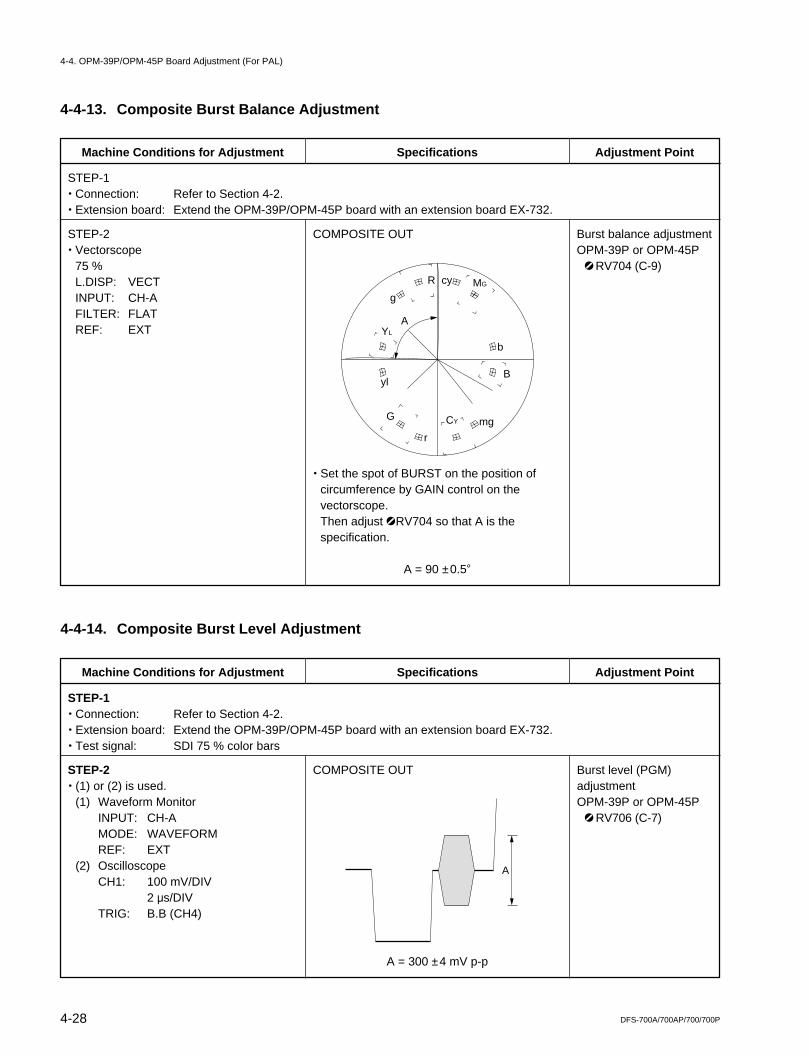
4-28 DFS-700A/700AP/700/700P
4-4-14. Composite Burst Level Adjustment
Machine Conditions for Adjustment Specifications Adjustment Point
COMPOSITE OUT
A = 300 ±4 mV p-p
Burst level (PGM)adjustmentOPM-39P or OPM-45P
1 RV706 (C-7)
STEP-1. Connection: Refer to Section 4-2.. Extension board: Extend the OPM-39P/OPM-45P board with an extension board EX-732.. Test signal: SDI 75 % color bars
STEP-2. (1) or (2) is used.
(1) Waveform MonitorINPUT: CH-AMODE: WAVEFORMREF: EXT
(2) OscilloscopeCH1: 100 mV/DIV
2 us/DIVTRIG: B.B (CH4)
A
Machine Conditions for Adjustment Specifications Adjustment Point
COMPOSITE OUT
. Set the spot of BURST on the position ofcircumference by GAIN control on thevectorscope.Then adjust 1RV704 so that A is thespecification.
A = 90 ±0.5d
Burst balance adjustmentOPM-39P or OPM-45P
1 RV704 (C-9)
STEP-1. Connection: Refer to Section 4-2.. Extension board: Extend the OPM-39P/OPM-45P board with an extension board EX-732.
STEP-2. Vectorscope
75 %L.DISP: VECTINPUT: CH-AFILTER: FLATREF: EXT
4-4-13. Composite Burst Balance Adjustment
A
R
g
G
r
B
b
MGcy
YL
yl
CY mg
4-4. OPM-39P/OPM-45P Board Adjustment (For PAL)
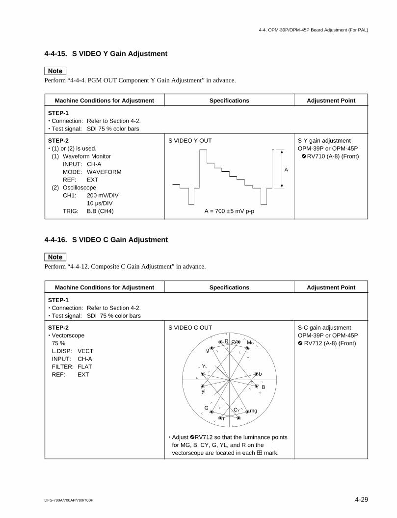
4-29DFS-700A/700AP/700/700P
4-4-15. S VIDEO Y Gain Adjustment
nPerform “4-4-4. PGM OUT Component Y Gain Adjustment” in advance.
Machine Conditions for Adjustment Specifications Adjustment Point
S VIDEO Y OUT
A = 700 ±5 mV p-p
S-Y gain adjustmentOPM-39P or OPM-45P
1 RV710 (A-8) (Front)
STEP-1. Connection: Refer to Section 4-2.. Test signal: SDI 75 % color bars
STEP-2. (1) or (2) is used.
(1) Waveform MonitorINPUT: CH-AMODE: WAVEFORMREF: EXT
(2) OscilloscopeCH1: 200 mV/DIV
10 us/DIVTRIG: B.B (CH4)
A
4-4. OPM-39P/OPM-45P Board Adjustment (For PAL)
4-4-16. S VIDEO C Gain Adjustment
nPerform “4-4-12. Composite C Gain Adjustment” in advance.
Machine Conditions for Adjustment Specifications Adjustment Point
S VIDEO C OUT
. Adjust 1RV712 so that the luminance pointsfor MG, B, CY, G, YL, and R on thevectorscope are located in each 4 mark.
S-C gain adjustmentOPM-39P or OPM-45P1 RV712 (A-8) (Front)
STEP-1. Connection: Refer to Section 4-2.. Test signal: SDI 75 % color bars
STEP-2. Vectorscope
75 %L.DISP: VECTINPUT: CH-AFILTER: FLATREF: EXT
R
g
G
r
B
b
MGcy
YL
yl
CY mg
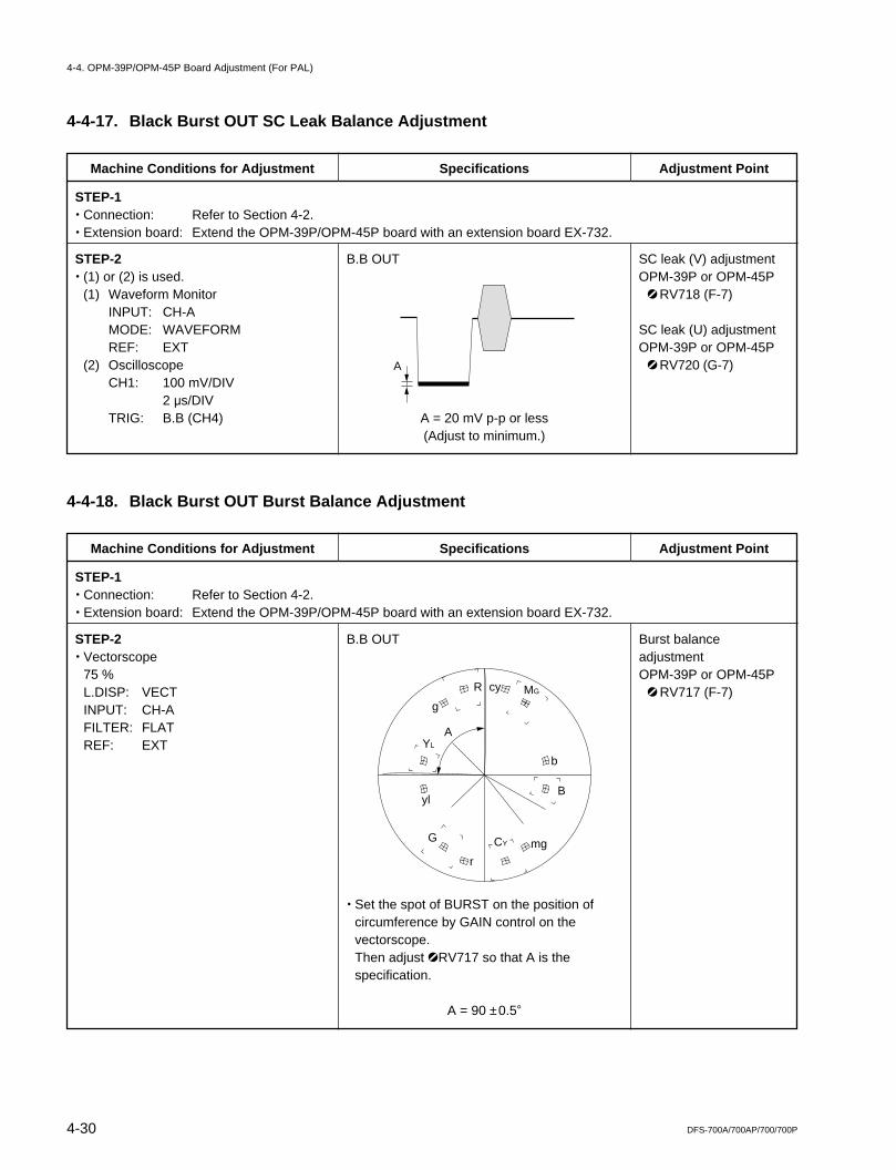
4-30 DFS-700A/700AP/700/700P
Machine Conditions for Adjustment Specifications Adjustment Point
B.B OUT
. Set the spot of BURST on the position ofcircumference by GAIN control on thevectorscope.Then adjust 1RV717 so that A is thespecification.
A = 90 ±0.5d
Burst balanceadjustmentOPM-39P or OPM-45P
1 RV717 (F-7)
STEP-1. Connection: Refer to Section 4-2.. Extension board: Extend the OPM-39P/OPM-45P board with an extension board EX-732.
STEP-2. Vectorscope
75 %L.DISP: VECTINPUT: CH-AFILTER: FLATREF: EXT
4-4-18. Black Burst OUT Burst Balance Adjustment
A
R
g
G
r
B
b
MGcy
YL
yl
CY mg
4-4-17. Black Burst OUT SC Leak Balance Adjustment
Machine Conditions for Adjustment Specifications Adjustment Point
B.B OUT
A = 20 mV p-p or less(Adjust to minimum.)
SC leak (V) adjustmentOPM-39P or OPM-45P
1 RV718 (F-7)
SC leak (U) adjustmentOPM-39P or OPM-45P
1 RV720 (G-7)
STEP-1. Connection: Refer to Section 4-2.. Extension board: Extend the OPM-39P/OPM-45P board with an extension board EX-732.
STEP-2. (1) or (2) is used.
(1) Waveform MonitorINPUT: CH-AMODE: WAVEFORMREF: EXT
(2) OscilloscopeCH1: 100 mV/DIV
2 us/DIVTRIG: B.B (CH4)
A
4-4. OPM-39P/OPM-45P Board Adjustment (For PAL)
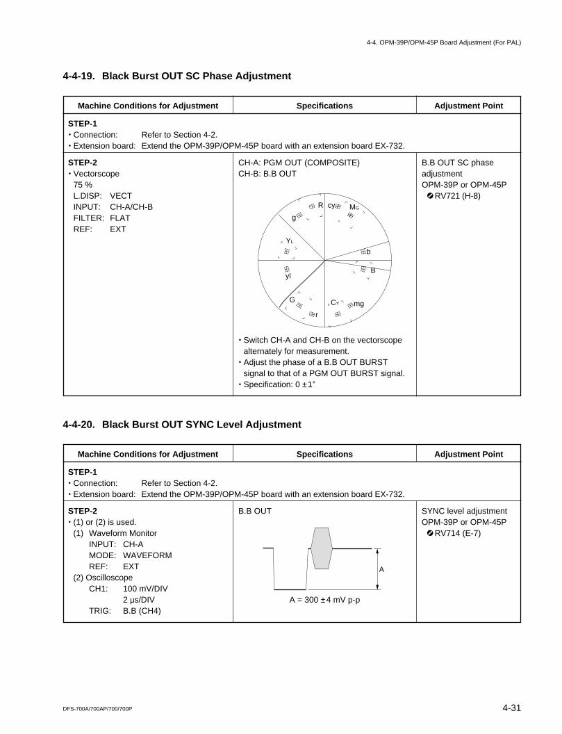
4-31DFS-700A/700AP/700/700P
4-4-19. Black Burst OUT SC Phase Adjustment
4-4. OPM-39P/OPM-45P Board Adjustment (For PAL)
Machine Conditions for Adjustment Specifications Adjustment Point
CH-A: PGM OUT (COMPOSITE)CH-B: B.B OUT
. Switch CH-A and CH-B on the vectorscopealternately for measurement.
. Adjust the phase of a B.B OUT BURSTsignal to that of a PGM OUT BURST signal.
. Specification: 0 ±1d
B.B OUT SC phaseadjustmentOPM-39P or OPM-45P
1 RV721 (H-8)
STEP-1. Connection: Refer to Section 4-2.. Extension board: Extend the OPM-39P/OPM-45P board with an extension board EX-732.
STEP-2. Vectorscope
75 %L.DISP: VECTINPUT: CH-A/CH-BFILTER: FLATREF: EXT
R
g
G
r
B
b
MGcy
YL
yl
CY mg
4-4-20. Black Burst OUT SYNC Level Adjustment
Machine Conditions for Adjustment Specifications Adjustment Point
B.B OUT
A = 300 ±4 mV p-p
SYNC level adjustmentOPM-39P or OPM-45P
1 RV714 (E-7)
STEP-1. Connection: Refer to Section 4-2.. Extension board: Extend the OPM-39P/OPM-45P board with an extension board EX-732.
STEP-2. (1) or (2) is used.
(1) Waveform MonitorINPUT: CH-AMODE: WAVEFORMREF: EXT
(2) OscilloscopeCH1: 100 mV/DIV
2 us/DIVTRIG: B.B (CH4)
A
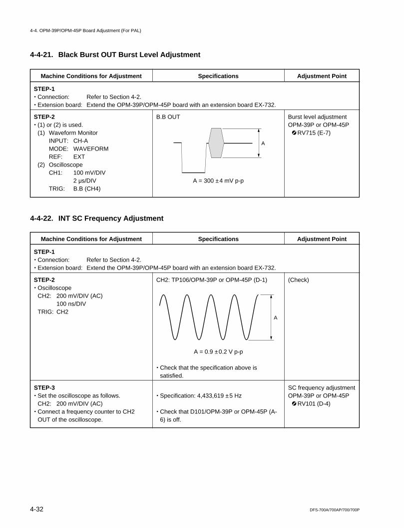
4-32 DFS-700A/700AP/700/700P
4-4-22. INT SC Frequency Adjustment
Machine Conditions for Adjustment Specifications Adjustment Point
CH2: TP106/OPM-39P or OPM-45P (D-1)
A = 0.9 ±0.2 V p-p
. Check that the specification above issatisfied.
. Specification: 4,433,619 ±5 Hz
. Check that D101/OPM-39P or OPM-45P (A-6) is off.
(Check)
SC frequency adjustmentOPM-39P or OPM-45P
1 RV101 (D-4)
STEP-1. Connection: Refer to Section 4-2.. Extension board: Extend the OPM-39P/OPM-45P board with an extension board EX-732.
STEP-2. Oscilloscope
CH2: 200 mV/DIV (AC)100 ns/DIV
TRIG: CH2
STEP-3. Set the oscilloscope as follows.
CH2: 200 mV/DIV (AC). Connect a frequency counter to CH2
OUT of the oscilloscope.
A
4-4-21. Black Burst OUT Burst Level Adjustment
Machine Conditions for Adjustment Specifications Adjustment Point
B.B OUT
A = 300 ±4 mV p-p
Burst level adjustmentOPM-39P or OPM-45P
1 RV715 (E-7)
STEP-1. Connection: Refer to Section 4-2.. Extension board: Extend the OPM-39P/OPM-45P board with an extension board EX-732.
STEP-2. (1) or (2) is used.
(1) Waveform MonitorINPUT: CH-AMODE: WAVEFORMREF: EXT
(2) OscilloscopeCH1: 100 mV/DIV
2 us/DIVTRIG: B.B (CH4)
A
4-4. OPM-39P/OPM-45P Board Adjustment (For PAL)
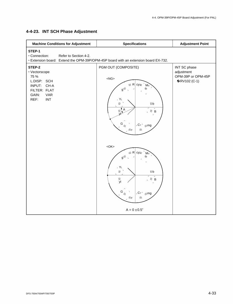
4-33DFS-700A/700AP/700/700P
4-4-23. INT SCH Phase Adjustment
4-4. OPM-39P/OPM-45P Board Adjustment (For PAL)
Machine Conditions for Adjustment Specifications Adjustment Point
PGM OUT (COMPOSITE)
A = 0 ±0.5d
INT SC phaseadjustmentOPM-39P or OPM-45P
1RV102 (C-1)
STEP-1. Connection: Refer to Section 4-2.. Extension board: Extend the OPM-39P/OPM-45P board with an extension board EX-732.
STEP-2. Vectorscope
75 %L.DISP: SCHINPUT: CH-AFILTER: FLATGAIN: VARREF: INT
A
R
g
G
r
B
b
MGcy
YL
yl
CY mg
R
g
G
r
B
b
MGcy
YL
yl
CY mg
<NG>
<OK>
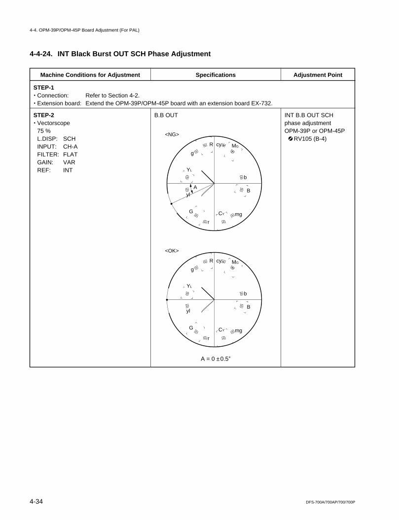
4-34 DFS-700A/700AP/700/700P
Machine Conditions for Adjustment Specifications Adjustment Point
B.B OUT
A = 0 ±0.5d
INT B.B OUT SCHphase adjustmentOPM-39P or OPM-45P
1 RV105 (B-4)
STEP-1. Connection: Refer to Section 4-2.. Extension board: Extend the OPM-39P/OPM-45P board with an extension board EX-732.
STEP-2. Vectorscope
75 %L.DISP: SCHINPUT: CH-AFILTER: FLATGAIN: VARREF: INT
A
R
g
G
r
B
b
MGcy
YL
yl
CY mg
R
g
G
r
B
b
MGcy
YL
yl
CY mg
<NG>
<OK>
4-4-24. INT Black Burst OUT SCH Phase Adjustment
4-4. OPM-39P/OPM-45P Board Adjustment (For PAL)
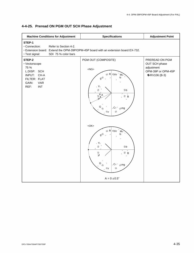
4-35DFS-700A/700AP/700/700P
Machine Conditions for Adjustment Specifications Adjustment Point
PGM OUT (COMPOSITE)
A = 0 ±0.5d
PREREAD ON PGMOUT SCH phaseadjustmentOPM-39P or OPM-45P
1 RV106 (B-3)
STEP-1. Connection: Refer to Section 4-2.. Extension board: Extend the OPM-39P/OPM-45P board with an extension board EX-732.. Test signal: SDI 75 % color bars
STEP-2. Vectorscope
75 %L.DISP: SCHINPUT: CH-AFILTER: FLATGAIN: VARREF: INT
4-4-25. Preread ON PGM OUT SCH Phase Adjustment
A
R
g
G
r
B
b
MGcy
YL
yl
CY mg
R
g
G
r
B
b
MGcy
YL
yl
CY mg
<NG>
<OK>
4-4. OPM-39P/OPM-45P Board Adjustment (For PAL)
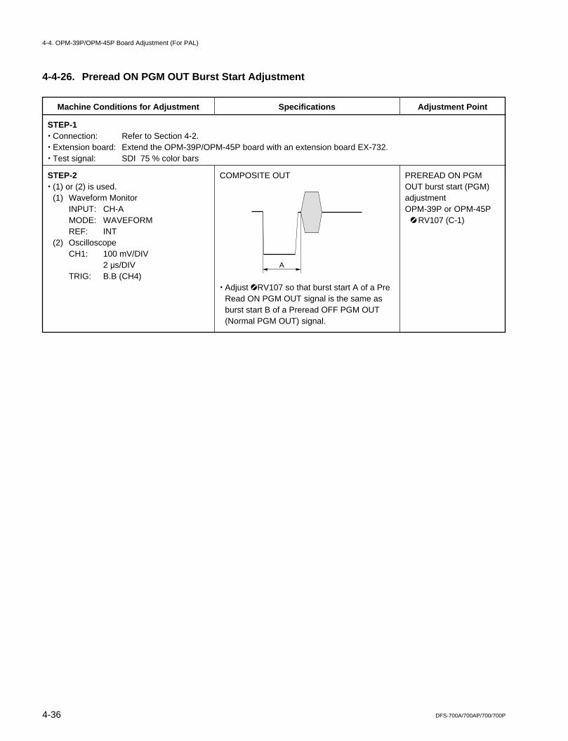
4-36 DFS-700A/700AP/700/700P
Machine Conditions for Adjustment Specifications Adjustment Point
COMPOSITE OUT
. Adjust 1RV107 so that burst start A of a PreRead ON PGM OUT signal is the same asburst start B of a Preread OFF PGM OUT(Normal PGM OUT) signal.
PREREAD ON PGMOUT burst start (PGM)adjustmentOPM-39P or OPM-45P
1 RV107 (C-1)
STEP-1. Connection: Refer to Section 4-2.. Extension board: Extend the OPM-39P/OPM-45P board with an extension board EX-732.. Test signal: SDI 75 % color bars
STEP-2. (1) or (2) is used.
(1) Waveform MonitorINPUT: CH-AMODE: WAVEFORMREF: INT
(2) OscilloscopeCH1: 100 mV/DIV
2 us/DIVTRIG: B.B (CH4)
4-4-26. Preread ON PGM OUT Burst Start Adjustment
A
4-4. OPM-39P/OPM-45P Board Adjustment (For PAL)
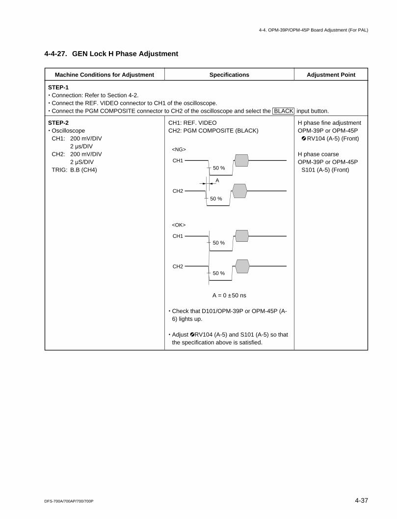
4-37DFS-700A/700AP/700/700P
Machine Conditions for Adjustment Specifications Adjustment Point
CH1: REF. VIDEOCH2: PGM COMPOSITE (BLACK)
A = 0 ±50 ns
. Check that D101/OPM-39P or OPM-45P (A-6) lights up.
. Adjust 1RV104 (A-5) and S101 (A-5) so thatthe specification above is satisfied.
H phase fine adjustmentOPM-39P or OPM-45P
1 RV104 (A-5) (Front)
H phase coarseOPM-39P or OPM-45P
S101 (A-5) (Front)
STEP-1. Connection: Refer to Section 4-2.. Connect the REF. VIDEO connector to CH1 of the oscilloscope.. Connect the PGM COMPOSITE connector to CH2 of the oscilloscope and select the BLACK input button.
STEP-2. Oscilloscope
CH1: 200 mV/DIV2 us/DIV
CH2: 200 mV/DIV2 uS/DIV
TRIG: B.B (CH4)
4-4-27. GEN Lock H Phase Adjustment
A
50 %CH1
<NG>
CH2
CH1
<OK>
CH2
50 %
50 %
50 %
4-4. OPM-39P/OPM-45P Board Adjustment (For PAL)
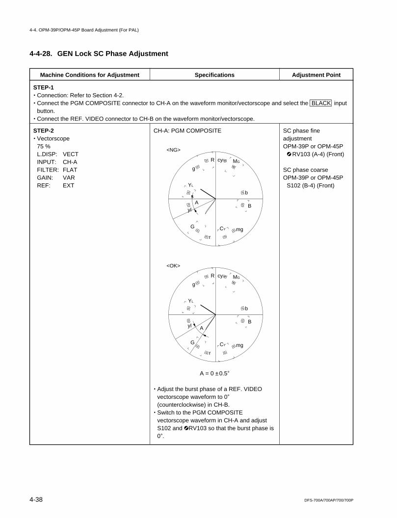
4-38 DFS-700A/700AP/700/700P
Machine Conditions for Adjustment Specifications Adjustment Point
CH-A: PGM COMPOSITE
A = 0 ±0.5d
. Adjust the burst phase of a REF. VIDEOvectorscope waveform to 0d(counterclockwise) in CH-B.
. Switch to the PGM COMPOSITEvectorscope waveform in CH-A and adjustS102 and 1RV103 so that the burst phase is0d.
SC phase fineadjustmentOPM-39P or OPM-45P
1 RV103 (A-4) (Front)
SC phase coarseOPM-39P or OPM-45P
S102 (B-4) (Front)
STEP-1. Connection: Refer to Section 4-2.. Connect the PGM COMPOSITE connector to CH-A on the waveform monitor/vectorscope and select the BLACK input
button.. Connect the REF. VIDEO connector to CH-B on the waveform monitor/vectorscope.
STEP-2. Vectorscope
75 %L.DISP: VECTINPUT: CH-AFILTER: FLATGAIN: VARREF: EXT
A
A
R
g
G
r
B
b
MGcy
YL
yl
CY mg
R
g
G
r
B
b
MGcy
YL
yl
CY mg
<NG>
<OK>
4-4-28. GEN Lock SC Phase Adjustment
4-4. OPM-39P/OPM-45P Board Adjustment (For PAL)
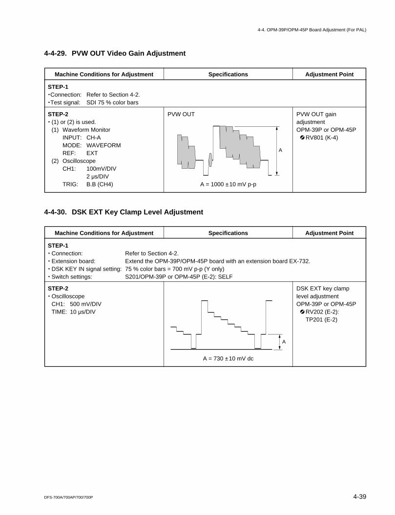
4-39DFS-700A/700AP/700/700P
4-4-29. PVW OUT Video Gain Adjustment
Machine Conditions for Adjustment Specifications Adjustment Point
PVW OUT
A = 1000 ±10 mV p-p
PVW OUT gainadjustmentOPM-39P or OPM-45P
1 RV801 (K-4)
STEP-1.Connection: Refer to Section 4-2..Test signal: SDI 75 % color bars
STEP-2. (1) or (2) is used.
(1) Waveform MonitorINPUT: CH-AMODE: WAVEFORMREF: EXT
(2) OscilloscopeCH1: 100mV/DIV
2 us/DIVTRIG: B.B (CH4)
A
4-4. OPM-39P/OPM-45P Board Adjustment (For PAL)
4-4-30. DSK EXT Key Clamp Level Adjustment
Machine Conditions for Adjustment Specifications Adjustment Point
A = 730 ±10 mV dc
DSK EXT key clamplevel adjustmentOPM-39P or OPM-45P
1 RV202 (E-2):TP201 (E-2)
STEP-1. Connection: Refer to Section 4-2.. Extension board: Extend the OPM-39P/OPM-45P board with an extension board EX-732.. DSK KEY IN signal setting: 75 % color bars = 700 mV p-p (Y only). Switch settings: S201/OPM-39P or OPM-45P (E-2): SELF
STEP-2. Oscilloscope
CH1: 500 mV/DIVTIME: 10 us/DIV
A
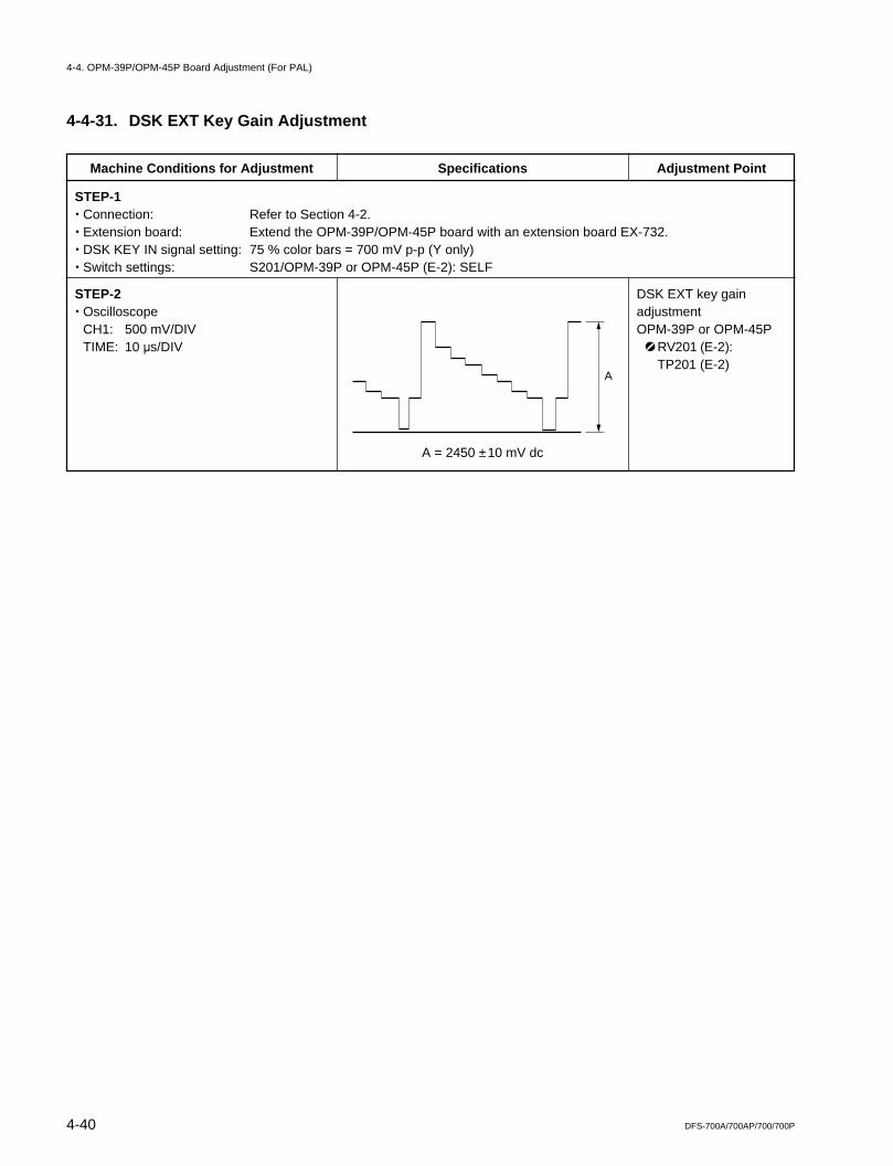
4-40 DFS-700A/700AP/700/700P
4-4-31. DSK EXT Key Gain Adjustment
Machine Conditions for Adjustment Specifications Adjustment Point
A = 2450 ±10 mV dc
DSK EXT key gainadjustmentOPM-39P or OPM-45P
1 RV201 (E-2):TP201 (E-2)
STEP-1. Connection: Refer to Section 4-2.. Extension board: Extend the OPM-39P/OPM-45P board with an extension board EX-732.. DSK KEY IN signal setting: 75 % color bars = 700 mV p-p (Y only). Switch settings: S201/OPM-39P or OPM-45P (E-2): SELF
STEP-2. Oscilloscope
CH1: 500 mV/DIVTIME: 10 us/DIV
A
4-4. OPM-39P/OPM-45P Board Adjustment (For PAL)
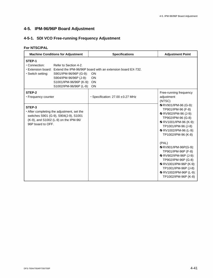
4-41DFS-700A/700AP/700/700P
4-5. IPM-96/96P Board Adjustment
4-5-1. SDI VCO Free-running Frequency Adjustment
For NTSC/PAL
Machine Conditions for Adjustment Specifications Adjustment Point
. Specification: 27.00 ±0.27 MHzFree-running frequencyadjustment(NTSC)1RV901/IPM-96 (G-9):
TP901/IPM-96 (F-8)1 RV902/IPM-96 (J-9):
TP902/IPM-96 (G-8)1 RV1001/IPM-96 (K-9):
TP1001/IPM-96 (J-8)1 RV1002/IPM-96 (L-9):
TP1002/IPM-96 (K-8)
(PAL)1RV901/IPM-96P(G-9):
TP901/IPM-96P (F-8)1 RV902/IPM-96P (J-9):
TP902/IPM-96P (G-8)1 RV1001/IPM-96P (K-9):
TP1001/IPM-96P (J-8)1 RV1002/IPM-96P (L-9):
TP1002/IPM-96P (K-8)
STEP-1. Connection: Refer to Section 4-2.. Extension board: Extend the IPM-96/96P board with an extension board EX-732.. Switch setting: S901/IPM-96/96P (G-9): ON
S904/IPM-96/96P (J-9): ONS1001/IPM-96/96P (K-9): ONS1002/IPM-96/96P (L-9): ON
STEP-2. Frequency counter
STEP-3. After completing the adjustment, set the
switches S901 (G-9), S904(J-9), S1001(K-9), and S1002 (L-9) on the IPM-96/96P board to OFF.
4-5. IPM-96/96P Board Adjustment
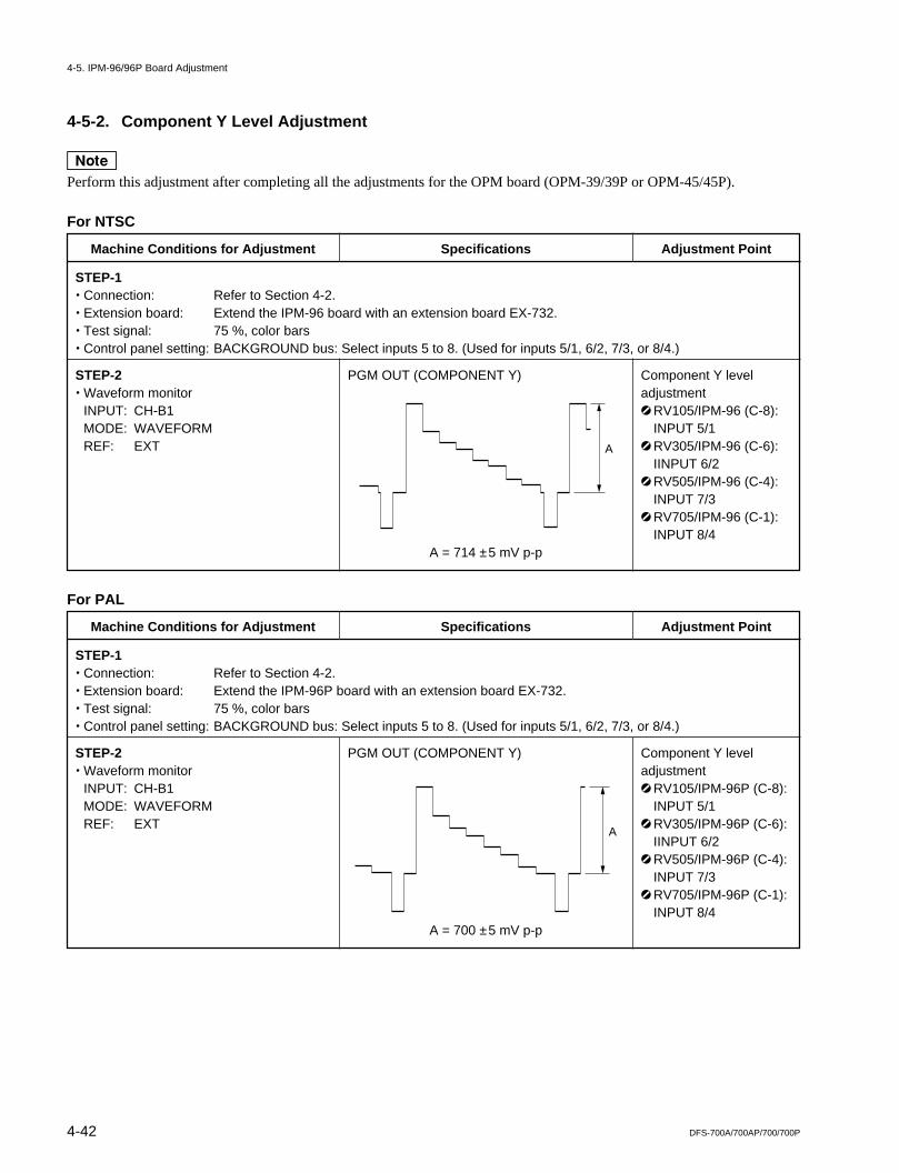
4-42 DFS-700A/700AP/700/700P
4-5-2. Component Y Level Adjustment
nPerform this adjustment after completing all the adjustments for the OPM board (OPM-39/39P or OPM-45/45P).
For NTSC
Machine Conditions for Adjustment Specifications Adjustment Point
PGM OUT (COMPONENT Y)
A = 714 ±5 mV p-p
Component Y leveladjustment1RV105/IPM-96 (C-8):
INPUT 5/11RV305/IPM-96 (C-6):
IINPUT 6/21RV505/IPM-96 (C-4):
INPUT 7/31RV705/IPM-96 (C-1):
INPUT 8/4
STEP-1. Connection: Refer to Section 4-2.. Extension board: Extend the IPM-96 board with an extension board EX-732.. Test signal: 75 %, color bars. Control panel setting: BACKGROUND bus: Select inputs 5 to 8. (Used for inputs 5/1, 6/2, 7/3, or 8/4.)
STEP-2. Waveform monitor
INPUT: CH-B1MODE: WAVEFORMREF: EXT A
For PAL
Machine Conditions for Adjustment Specifications Adjustment Point
PGM OUT (COMPONENT Y)
A = 700 ±5 mV p-p
Component Y leveladjustment1RV105/IPM-96P (C-8):
INPUT 5/11RV305/IPM-96P (C-6):
IINPUT 6/21RV505/IPM-96P (C-4):
INPUT 7/31RV705/IPM-96P (C-1):
INPUT 8/4
STEP-1. Connection: Refer to Section 4-2.. Extension board: Extend the IPM-96P board with an extension board EX-732.. Test signal: 75 %, color bars. Control panel setting: BACKGROUND bus: Select inputs 5 to 8. (Used for inputs 5/1, 6/2, 7/3, or 8/4.)
STEP-2. Waveform monitor
INPUT: CH-B1MODE: WAVEFORMREF: EXT
A
4-5. IPM-96/96P Board Adjustment
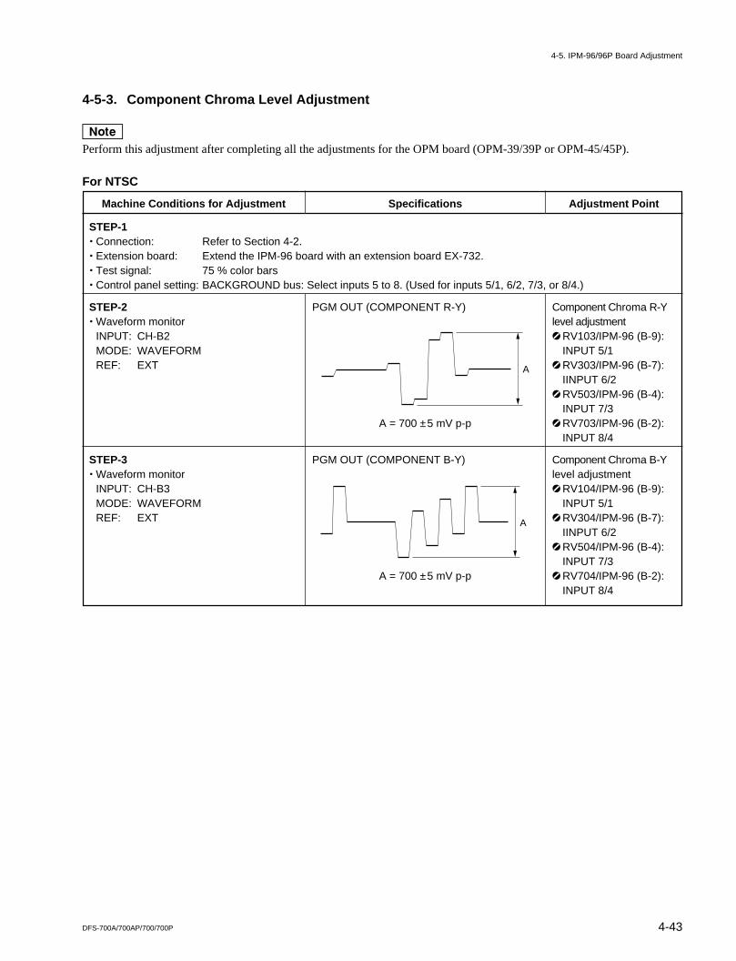
4-43DFS-700A/700AP/700/700P
4-5-3. Component Chroma Level Adjustment
nPerform this adjustment after completing all the adjustments for the OPM board (OPM-39/39P or OPM-45/45P).
For NTSC
Machine Conditions for Adjustment Specifications Adjustment Point
PGM OUT (COMPONENT R-Y)
A = 700 ±5 mV p-p
PGM OUT (COMPONENT B-Y)
A = 700 ±5 mV p-p
Component Chroma R-Ylevel adjustment1RV103/IPM-96 (B-9):
INPUT 5/11RV303/IPM-96 (B-7):
IINPUT 6/21RV503/IPM-96 (B-4):
INPUT 7/31RV703/IPM-96 (B-2):
INPUT 8/4
Component Chroma B-Ylevel adjustment1RV104/IPM-96 (B-9):
INPUT 5/11RV304/IPM-96 (B-7):
IINPUT 6/21RV504/IPM-96 (B-4):
INPUT 7/31RV704/IPM-96 (B-2):
INPUT 8/4
STEP-1. Connection: Refer to Section 4-2.. Extension board: Extend the IPM-96 board with an extension board EX-732.. Test signal: 75 % color bars. Control panel setting: BACKGROUND bus: Select inputs 5 to 8. (Used for inputs 5/1, 6/2, 7/3, or 8/4.)
STEP-2. Waveform monitor
INPUT: CH-B2MODE: WAVEFORMREF: EXT
STEP-3. Waveform monitor
INPUT: CH-B3MODE: WAVEFORMREF: EXT
A
A
4-5. IPM-96/96P Board Adjustment
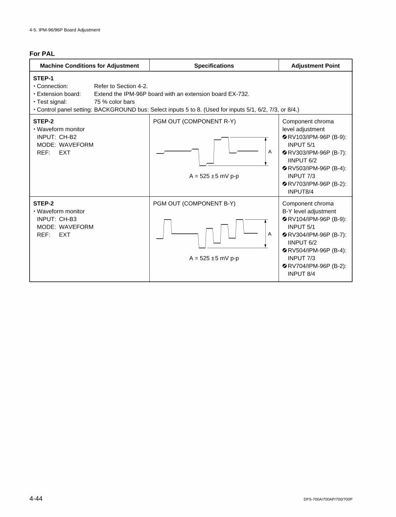
4-44 DFS-700A/700AP/700/700P
For PAL
Machine Conditions for Adjustment Specifications Adjustment Point
PGM OUT (COMPONENT R-Y)
A = 525 ±5 mV p-p
PGM OUT (COMPONENT B-Y)
A = 525 ±5 mV p-p
Component chromalevel adjustment1RV103/IPM-96P (B-9):
INPUT 5/11RV303/IPM-96P (B-7):
IINPUT 6/21RV503/IPM-96P (B-4):
INPUT 7/31RV703/IPM-96P (B-2):
INPUT8/4
Component chromaB-Y level adjustment1RV104/IPM-96P (B-9):
INPUT 5/11RV304/IPM-96P (B-7):
IINPUT 6/21RV504/IPM-96P (B-4):
INPUT 7/31RV704/IPM-96P (B-2):
INPUT 8/4
STEP-1. Connection: Refer to Section 4-2.. Extension board: Extend the IPM-96P board with an extension board EX-732.. Test signal: 75 % color bars. Control panel setting: BACKGROUND bus: Select inputs 5 to 8. (Used for inputs 5/1, 6/2, 7/3, or 8/4.)
STEP-2. Waveform monitor
INPUT: CH-B2MODE: WAVEFORMREF: EXT
STEP-2. Waveform monitor
INPUT: CH-B3MODE: WAVEFORMREF: EXT
A
A
4-5. IPM-96/96P Board Adjustment
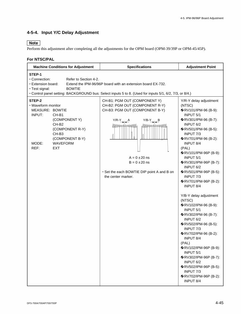
4-45DFS-700A/700AP/700/700P
4-5-4. Input Y/C Delay Adjustment
nPerform this adjustment after completing all the adjustments for the OPM board (OPM-39/39P or OPM-45/45P).
For NTSC/PAL
Machine Conditions for Adjustment Specifications Adjustment Point
CH-B1: PGM OUT (COMPONENT Y)CH-B2: PGM OUT (COMPONENT R-Y)CH-B3: PGM OUT (COMPONENT B-Y)
A = 0 ±20 nsB = 0 ±20 ns
. Set the each BOWTIE DIP point A and B onthe center marker.
Y/R-Y delay adjustment(NTSC)1RV101/IPM-96 (B-9):
INPUT 5/11RV301/IPM-96 (B-7):
INPUT 6/21RV501/IPM-96 (B-5):
INPUT 7/31RV701/IPM-96 (B-2):
INPUT 8/4(PAL)1RV101/IPM-96P (B-9):
INPUT 5/11RV301/IPM-96P (B-7):
INPUT 6/21RV501/IPM-96P (B-5):
INPUT 7/31RV701/IPM-96P (B-2):
INPUT 8/4
Y/B-Y delay adjustment(NTSC)1RV102/IPM-96 (B-9):
INPUT 5/11RV302/IPM-96 (B-7):
INPUT 6/21RV502/IPM-96 (B-5):
INPUT 7/31RV702/IPM-96 (B-2):
INPUT 8/4(PAL)1RV102/IPM-96P (B-9):
INPUT 5/11RV302/IPM-96P (B-7):
INPUT 6/21RV502/IPM-96P (B-5):
INPUT 7/31RV702/IPM-96P (B-2):
INPUT 8/4
STEP-1. Connection: Refer to Section 4-2.. Extension board: Extend the IPM-96/96P board with an extension board EX-732.. Test signal: BOWTIE. Control panel setting: BACKGROUND bus: Select inputs 5 to 8. (Used for inputs 5/1, 6/2, 7/3, or 8/4.)
STEP-2. Waveform monitor
MEASURE: BOWTIEINPUT: CH-B1
(COMPONENT Y)CH-B2(COMPONENT R-Y)CH-B3(COMPONENT B-Y)
MODE: WAVEFORMREF: EXT
AY/R-Y BY/B-Y
4-5. IPM-96/96P Board Adjustment
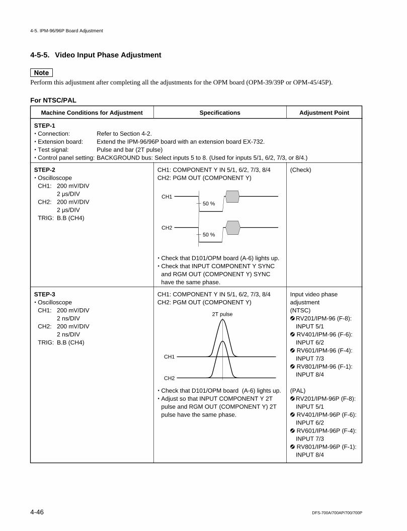
4-46 DFS-700A/700AP/700/700P
4-5-5. Video Input Phase Adjustment
nPerform this adjustment after completing all the adjustments for the OPM board (OPM-39/39P or OPM-45/45P).
For NTSC/PAL
Machine Conditions for Adjustment Specifications Adjustment Point
CH1: COMPONENT Y IN 5/1, 6/2, 7/3, 8/4CH2: PGM OUT (COMPONENT Y)
. Check that D101/OPM board (A-6) lights up.
. Check that INPUT COMPONENT Y SYNCand RGM OUT (COMPONENT Y) SYNChave the same phase.
CH1: COMPONENT Y IN 5/1, 6/2, 7/3, 8/4CH2: PGM OUT (COMPONENT Y)
. Check that D101/OPM board (A-6) lights up.
. Adjust so that INPUT COMPONENT Y 2Tpulse and RGM OUT (COMPONENT Y) 2Tpulse have the same phase.
(Check)
Input video phaseadjustment(NTSC)1RV201/IPM-96 (F-8):
INPUT 5/11 RV401/IPM-96 (F-6):
INPUT 6/21 RV601/IPM-96 (F-4):
INPUT 7/31 RV801/IPM-96 (F-1):
INPUT 8/4
(PAL)1RV201/IPM-96P (F-8):
INPUT 5/11 RV401/IPM-96P (F-6):
INPUT 6/21 RV601/IPM-96P (F-4):
INPUT 7/31 RV801/IPM-96P (F-1):
INPUT 8/4
STEP-1. Connection: Refer to Section 4-2.. Extension board: Extend the IPM-96/96P board with an extension board EX-732.. Test signal: Pulse and bar (2T pulse). Control panel setting: BACKGROUND bus: Select inputs 5 to 8. (Used for inputs 5/1, 6/2, 7/3, or 8/4.)
STEP-2. Oscilloscope
CH1: 200 mV/DIV2 us/DIV
CH2: 200 mV/DIV2 us/DIV
TRIG: B.B (CH4)
STEP-3. Oscilloscope
CH1: 200 mV/DIV2 ns/DIV
CH2: 200 mV/DIV2 ns/DIV
TRIG: B.B (CH4)
CH1
CH2
50 %
50 %
CH1
CH2
2T pulse
4-5. IPM-96/96P Board Adjustment
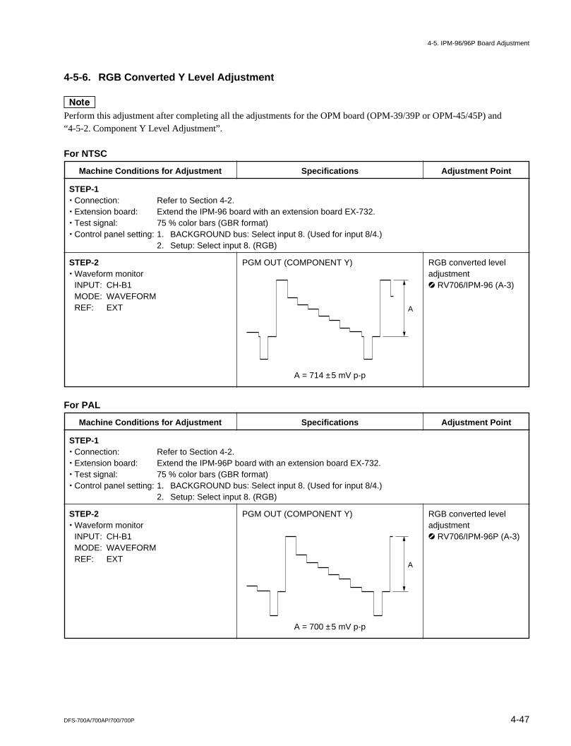
4-47DFS-700A/700AP/700/700P
4-5-6. RGB Converted Y Level Adjustment
nPerform this adjustment after completing all the adjustments for the OPM board (OPM-39/39P or OPM-45/45P) and“4-5-2. Component Y Level Adjustment”.
For NTSC
Machine Conditions for Adjustment Specifications Adjustment Point
PGM OUT (COMPONENT Y)
A = 714 ±5 mV p-p
RGB converted leveladjustment1 RV706/IPM-96 (A-3)
STEP-1. Connection: Refer to Section 4-2.. Extension board: Extend the IPM-96 board with an extension board EX-732.. Test signal: 75 % color bars (GBR format). Control panel setting: 1. BACKGROUND bus: Select input 8. (Used for input 8/4.)
2. Setup: Select input 8. (RGB)
STEP-2. Waveform monitor
INPUT: CH-B1MODE: WAVEFORMREF: EXT
A
A
For PAL
Machine Conditions for Adjustment Specifications Adjustment Point
PGM OUT (COMPONENT Y)
A = 700 ±5 mV p-p
RGB converted leveladjustment1 RV706/IPM-96P (A-3)
STEP-1. Connection: Refer to Section 4-2.. Extension board: Extend the IPM-96P board with an extension board EX-732.. Test signal: 75 % color bars (GBR format). Control panel setting: 1. BACKGROUND bus: Select input 8. (Used for input 8/4.)
2. Setup: Select input 8. (RGB)
STEP-2. Waveform monitor
INPUT: CH-B1MODE: WAVEFORMREF: EXT
4-5. IPM-96/96P Board Adjustment
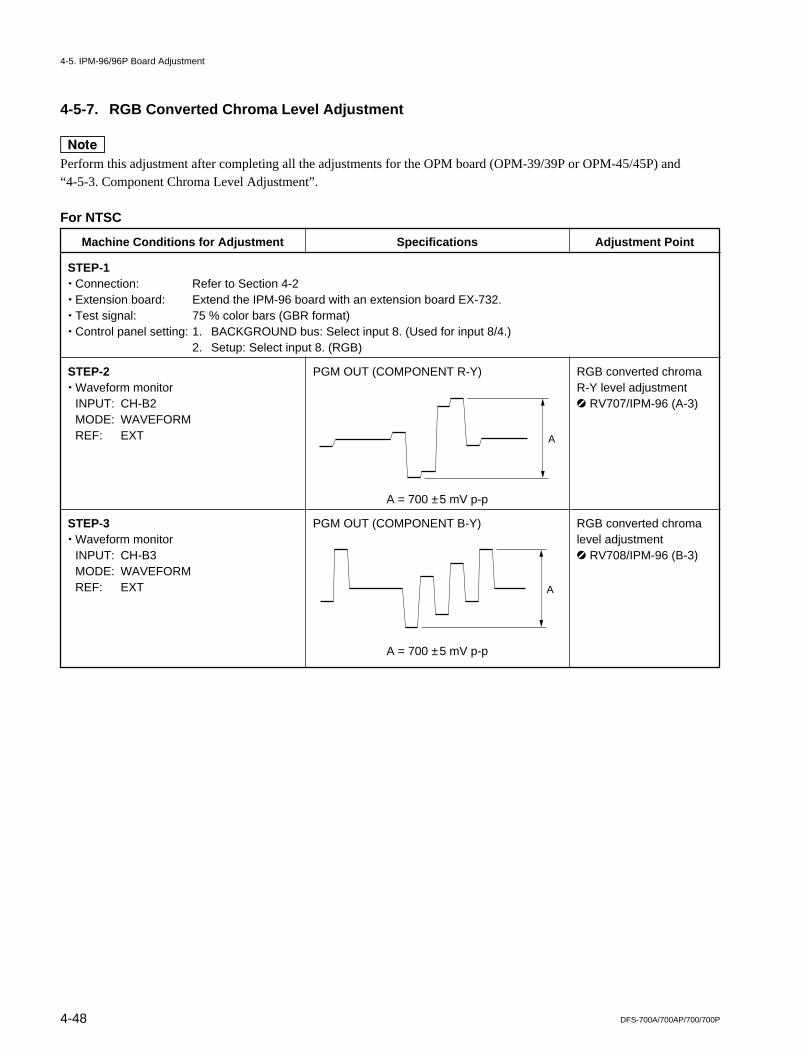
4-48 DFS-700A/700AP/700/700P
4-5. IPM-96/96P Board Adjustment
4-5-7. RGB Converted Chroma Level Adjustment
nPerform this adjustment after completing all the adjustments for the OPM board (OPM-39/39P or OPM-45/45P) and“4-5-3. Component Chroma Level Adjustment”.
For NTSC
Machine Conditions for Adjustment Specifications Adjustment Point
PGM OUT (COMPONENT R-Y)
A = 700 ±5 mV p-p
PGM OUT (COMPONENT B-Y)
A = 700 ±5 mV p-p
RGB converted chromaR-Y level adjustment1 RV707/IPM-96 (A-3)
RGB converted chromalevel adjustment1 RV708/IPM-96 (B-3)
STEP-1. Connection: Refer to Section 4-2. Extension board: Extend the IPM-96 board with an extension board EX-732.. Test signal: 75 % color bars (GBR format). Control panel setting: 1. BACKGROUND bus: Select input 8. (Used for input 8/4.)
2. Setup: Select input 8. (RGB)
STEP-2. Waveform monitor
INPUT: CH-B2MODE: WAVEFORMREF: EXT
STEP-3. Waveform monitor
INPUT: CH-B3MODE: WAVEFORMREF: EXT
A
A
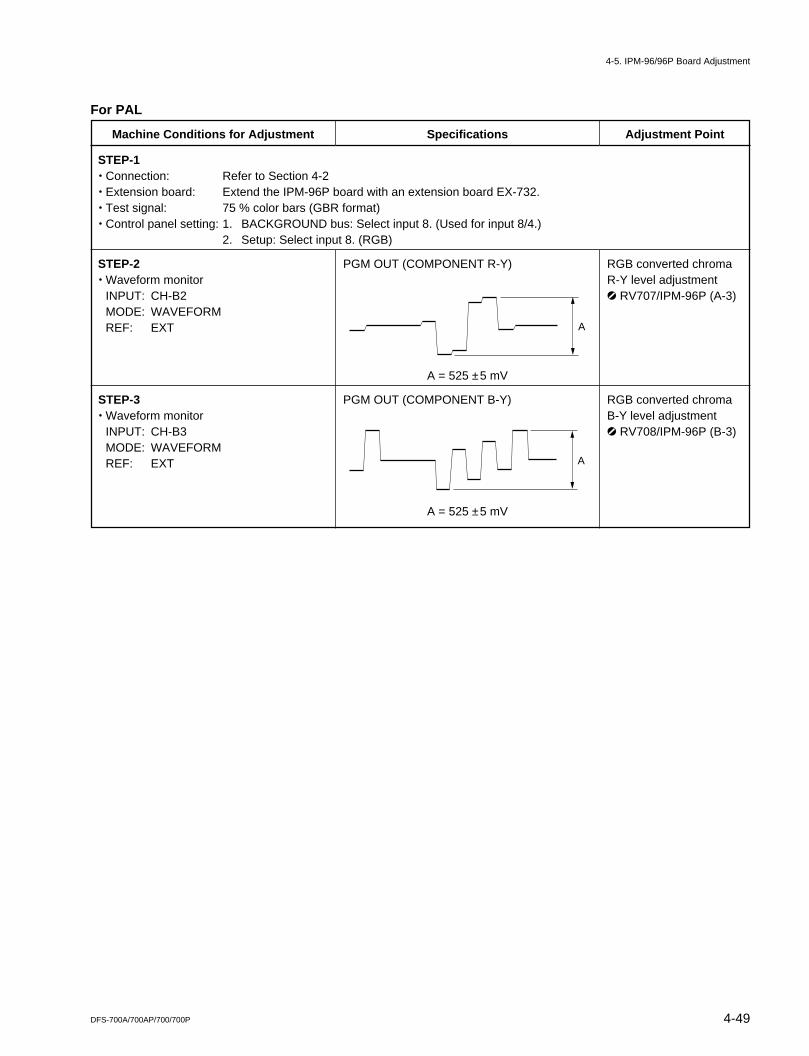
4-49DFS-700A/700AP/700/700P
4-5. IPM-96/96P Board Adjustment
For PAL
Machine Conditions for Adjustment Specifications Adjustment Point
PGM OUT (COMPONENT R-Y)
A = 525 ±5 mV
PGM OUT (COMPONENT B-Y)
A = 525 ±5 mV
RGB converted chromaR-Y level adjustment1 RV707/IPM-96P (A-3)
RGB converted chromaB-Y level adjustment1 RV708/IPM-96P (B-3)
STEP-1. Connection: Refer to Section 4-2. Extension board: Extend the IPM-96P board with an extension board EX-732.. Test signal: 75 % color bars (GBR format). Control panel setting: 1. BACKGROUND bus: Select input 8. (Used for input 8/4.)
2. Setup: Select input 8. (RGB)
STEP-2. Waveform monitor
INPUT: CH-B2MODE: WAVEFORMREF: EXT
STEP-3. Waveform monitor
INPUT: CH-B3MODE: WAVEFORMREF: EXT A
A
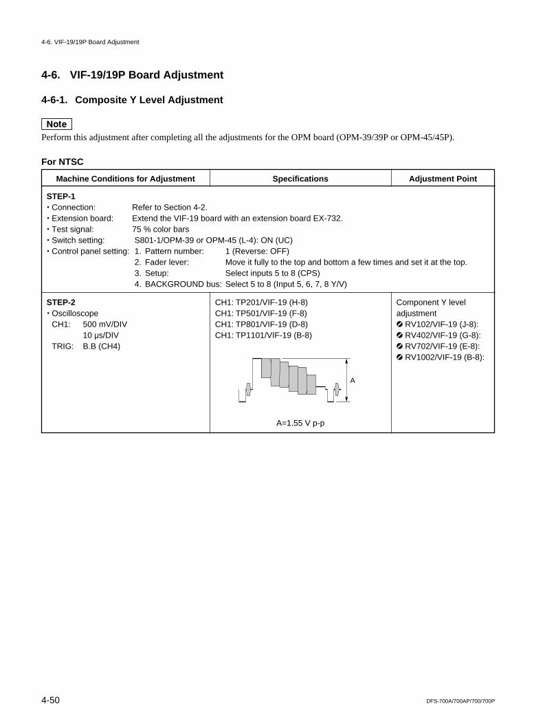
4-50 DFS-700A/700AP/700/700P
Machine Conditions for Adjustment Specifications Adjustment Point
CH1: TP201/VIF-19 (H-8)CH1: TP501/VIF-19 (F-8)CH1: TP801/VIF-19 (D-8)CH1: TP1101/VIF-19 (B-8)
A=1.55 V p-p
Component Y leveladjustment1 RV102/VIF-19 (J-8):1 RV402/VIF-19 (G-8):1 RV702/VIF-19 (E-8):1 RV1002/VIF-19 (B-8):
STEP-1. Connection: Refer to Section 4-2.. Extension board: Extend the VIF-19 board with an extension board EX-732.. Test signal: 75 % color bars. Switch setting: S801-1/OPM-39 or OPM-45 (L-4): ON (UC). Control panel setting: 1. Pattern number: 1 (Reverse: OFF)
2. Fader lever: Move it fully to the top and bottom a few times and set it at the top.3. Setup: Select inputs 5 to 8 (CPS)4. BACKGROUND bus: Select 5 to 8 (Input 5, 6, 7, 8 Y/V)
STEP-2. Oscilloscope
CH1: 500 mV/DIV10 us/DIV
TRIG: B.B (CH4)
4-6. VIF-19/19P Board Adjustment
4-6-1. Composite Y Level Adjustment
nPerform this adjustment after completing all the adjustments for the OPM board (OPM-39/39P or OPM-45/45P).
For NTSC
A
4-6. VIF-19/19P Board Adjustment
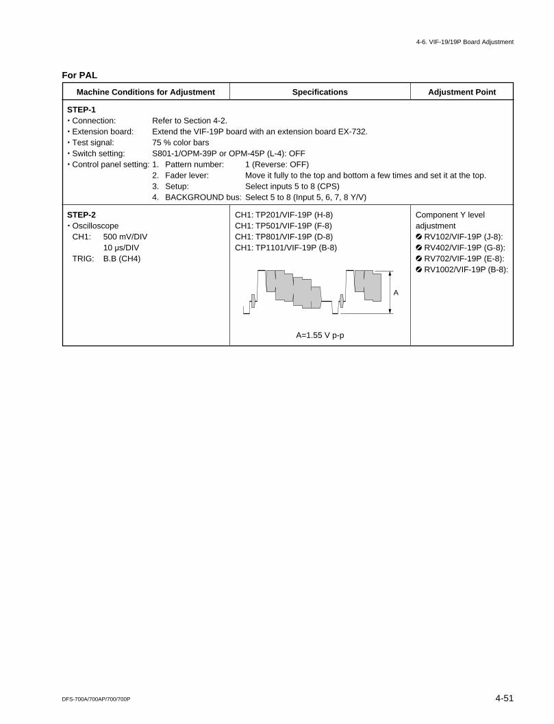
4-51DFS-700A/700AP/700/700P
Machine Conditions for Adjustment Specifications Adjustment Point
CH1: TP201/VIF-19P (H-8)CH1: TP501/VIF-19P (F-8)CH1: TP801/VIF-19P (D-8)CH1: TP1101/VIF-19P (B-8)
A=1.55 V p-p
Component Y leveladjustment1 RV102/VIF-19P (J-8):1 RV402/VIF-19P (G-8):1 RV702/VIF-19P (E-8):1 RV1002/VIF-19P (B-8):
STEP-1. Connection: Refer to Section 4-2.. Extension board: Extend the VIF-19P board with an extension board EX-732.. Test signal: 75 % color bars. Switch setting: S801-1/OPM-39P or OPM-45P (L-4): OFF. Control panel setting: 1. Pattern number: 1 (Reverse: OFF)
2. Fader lever: Move it fully to the top and bottom a few times and set it at the top.3. Setup: Select inputs 5 to 8 (CPS)4. BACKGROUND bus: Select 5 to 8 (Input 5, 6, 7, 8 Y/V)
STEP-2. Oscilloscope
CH1: 500 mV/DIV10 us/DIV
TRIG: B.B (CH4)
For PAL
A
4-6. VIF-19/19P Board Adjustment
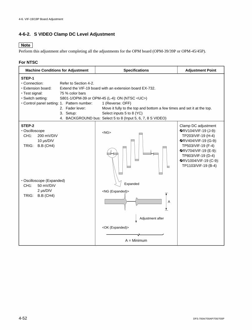
4-52 DFS-700A/700AP/700/700P
4-6-2. S VIDEO Clamp DC Level Adjustment
nPerform this adjustment after completing all the adjustments for the OPM board (OPM-39/39P or OPM-45/45P).
For NTSC
Machine Conditions for Adjustment Specifications Adjustment Point
A = Minimum
Clamp DC adjustment1RV104/VIF-19 (J-9):
TP203/VIF-19 (H-4)1RV404/VIF-19 (G-9):
TP503/VIF-19 (F-4)1RV704/VIF-19 (E-9):
TP803/VIF-19 (D-4)1RV1004/VIF-19 (C-9):
TP1103/VIF-19 (B-4)
STEP-1. Connection: Refer to Section 4-2.. Extension board: Extend the VIF-19 board with an extension board EX-732.. Test signal: 75 % color bars. Switch setting: S801-1/OPM-39 or OPM-45 (L-4): ON (NTSC <UC>). Control panel setting: 1. Pattern number: 1 (Reverse: OFF)
2. Fader lever: Move it fully to the top and bottom a few times and set it at the top.3. Setup: Select inputs 5 to 8 (YC)4. BACKGROUND bus: Select 5 to 8 (Input 5, 6, 7, 8 S VIDEO)
STEP-2. Oscilloscope
CH1: 200 mV/DIV10 us/DIV
TRIG: B.B (CH4)
. Oscilloscope (Expanded)CH1: 50 mV/DIV
2 us/DIVTRIG: B.B (CH4)
4-6. VIF-19/19P Board Adjustment
A
<NG>
<NG (Expanded)>
Expanded
Adjustment after
<OK (Expanded)>
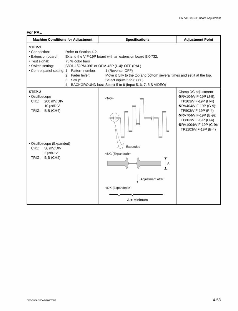
4-53DFS-700A/700AP/700/700P
For PAL
Machine Conditions for Adjustment Specifications Adjustment Point
A = Minimum
Clamp DC adjustment1RV104/VIF-19P (J-9):
TP203/VIF-19P (H-4)1RV404/VIF-19P (G-9):
TP503/VIF-19P (F-4)1RV704/VIF-19P (E-9):
TP803/VIF-19P (D-4)1RV1004/VIF-19P (C-9):
TP1103/VIF-19P (B-4)
STEP-1. Connection: Refer to Section 4-2.. Extension board: Extend the VIF-19P board with an extension board EX-732.. Test signal: 75 % color bars. Switch setting: S801-1/OPM-39P or OPM-45P (L-4): OFF (PAL). Control panel setting: 1. Pattern number: 1 (Reverse: OFF)
2. Fader lever: Move it fully to the top and bottom several times and set it at the top.3. Setup: Select inputs 5 to 8 (YC)4. BACKGROUND bus: Select 5 to 8 (Input 5, 6, 7, 8 S VIDEO)
STEP-2. Oscilloscope
CH1: 200 mV/DIV10 us/DIV
TRIG: B.B (CH4)
. Oscilloscope (Expanded)CH1: 50 mV/DIV
2 us/DIVTRIG: B.B (CH4)
4-6. VIF-19/19P Board Adjustment
A
<NG>
<NG (Expanded)>
Expanded
Adjustment after
<OK (Expanded)>
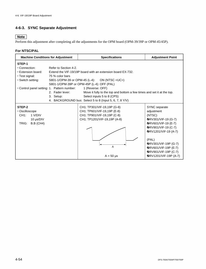
4-54 DFS-700A/700AP/700/700P
4-6-3. SYNC Separate Adjustment
nPerform this adjustment after completing all the adjustments for the OPM board (OPM-39/39P or OPM-45/45P).
For NTSC/PAL
Machine Conditions for Adjustment Specifications Adjustment Point
CH1: TP301/VIF-19,19P (G-8)CH1: TP601/VIF-19,19P (E-8)CH1: TP901/VIF-19,19P (C-8)CH1: TP1201/VIF-19,19P (A-8)
A = 50 us
SYNC separateadjustment(NTSC)1RV301/VIF-19 (G-7)1RV601/VIF-19 (E-7)1RV901/VIF-19 (C-7)1RV1201/VIF-19 (A-7)
(PAL)1RV301/VIF-19P (G-7)1RV601/VIF-19P (E-7)1RV901/VIF-19P (C-7)1RV1201/VIF-19P (A-7)
STEP-1. Connection: Refer to Section 4-2.. Extension board: Extend the VIF-19/19P board with an extension board EX-732.. Test signal: 75 % color bars. Switch setting: S801-1/OPM-39 or OPM-45 (L-4): ON (NTSC <UC>)
S801-1/OPM-39P or OPM-45P (L-4): OFF (PAL). Control panel setting: 1. Pattern number: 1 (Reverse: OFF)
2. Fader lever: Move it fully to the top and bottom a few times and set it at the top.3. Setup: Select inputs 5 to 8 (CPS)4. BACKGROUND bus: Select 5 to 8 (Input 5, 6, 7, 8 Y/V)
STEP-2. Oscilloscope
CH1: 1 V/DIV10 us/DIV
TRIG: B.B (CH4)
4-6. VIF-19/19P Board Adjustment
A
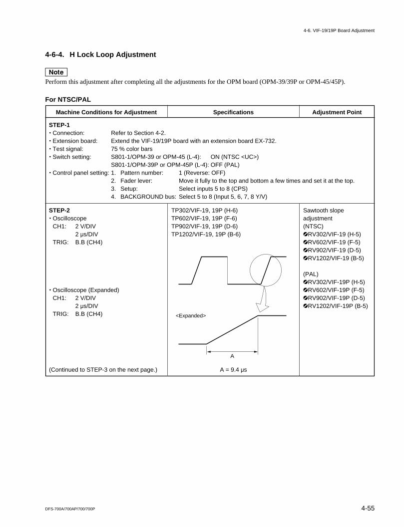
4-55DFS-700A/700AP/700/700P
4-6-4. H Lock Loop Adjustment
nPerform this adjustment after completing all the adjustments for the OPM board (OPM-39/39P or OPM-45/45P).
For NTSC/PAL
Machine Conditions for Adjustment Specifications Adjustment Point
TP302/VIF-19, 19P (H-6)TP602/VIF-19, 19P (F-6)TP902/VIF-19, 19P (D-6)TP1202/VIF-19, 19P (B-6)
A = 9.4 us
Sawtooth slopeadjustment(NTSC)1RV302/VIF-19 (H-5)1RV602/VIF-19 (F-5)1RV902/VIF-19 (D-5)1RV1202/VIF-19 (B-5)
(PAL)1RV302/VIF-19P (H-5)1RV602/VIF-19P (F-5)1RV902/VIF-19P (D-5)1RV1202/VIF-19P (B-5)
STEP-1. Connection: Refer to Section 4-2.. Extension board: Extend the VIF-19/19P board with an extension board EX-732.. Test signal: 75 % color bars. Switch setting: S801-1/OPM-39 or OPM-45 (L-4): ON (NTSC <UC>)
S801-1/OPM-39P or OPM-45P (L-4): OFF (PAL). Control panel setting: 1. Pattern number: 1 (Reverse: OFF)
2. Fader lever: Move it fully to the top and bottom a few times and set it at the top.3. Setup: Select inputs 5 to 8 (CPS)4. BACKGROUND bus: Select 5 to 8 (Input 5, 6, 7, 8 Y/V)
STEP-2. Oscilloscope
CH1: 2 V/DIV2 us/DIV
TRIG: B.B (CH4)
. Oscilloscope (Expanded)CH1: 2 V/DIV
2 us/DIVTRIG: B.B (CH4)
(Continued to STEP-3 on the next page.)
A
4-6. VIF-19/19P Board Adjustment
<Expanded>
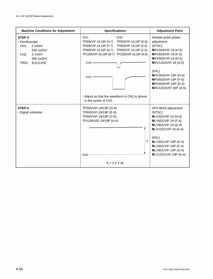
4-56 DFS-700A/700AP/700/700P
Machine Conditions for Adjustment Specifications Adjustment Point
STEP-3. Oscilloscope
CH1: 5 V/DIV500 ns/DIV
CH2: 2 V/DIV500 ns/DIV
TRIG: B.B (CH4)
STEP-4. Digital voltmeter
CH1: CH2:TP306/VIF-19,19P (H-7) TP303/VIF-19,19P (G-6)TP606/VIF-19,19P (F-7) TP603/VIF-19,19P (E-6)TP906/VIF-19,19P (D-7) TP903/VIF-19,19P (C-6)TP1206/VIF-19,19P (B-7) TP1203/VIF-19,19P (A-6)
. Adjust so that the waveform in CH2 is almostin the center of CH1.
TP305/VIF-19/19P (G-6)TP605/VIF-19/19P (E-6)TP905/VIF-19/19P (C-6)TP1205/VIF-19/19P (A-6)
A = 2.5 V dc
Sample pulse phaseadjustment(NTSC)1RV303/VIF-19 (H-5)1RV603/VIF-19 (F-5)1RV903/VIF-19 (D-5)1RV1203/VIF-19 (A-5)
(PAL)1RV303/VIF-19P (H-5)1RV603/VIF-19P (F-5)1RV903/VIF-19P (D-5)1RV1203/VIF-19P (A-5)
VFO BIAS adjustment(NTSC)1LV301/VIF-19 (H-4)1LV601/VIF-19 (F-4)1LV901/VIF-19 (D-4)1LV1201/VIF-19 (A-4)
(PAL)1LV301/VIF-19P (H-4)1LV601/VIF-19P (F-4)1LV901/VIF-19P (D-4)1LV1201/VIF-19P (A-4)
CH2
CH1
A
GND
4-6. VIF-19/19P Board Adjustment
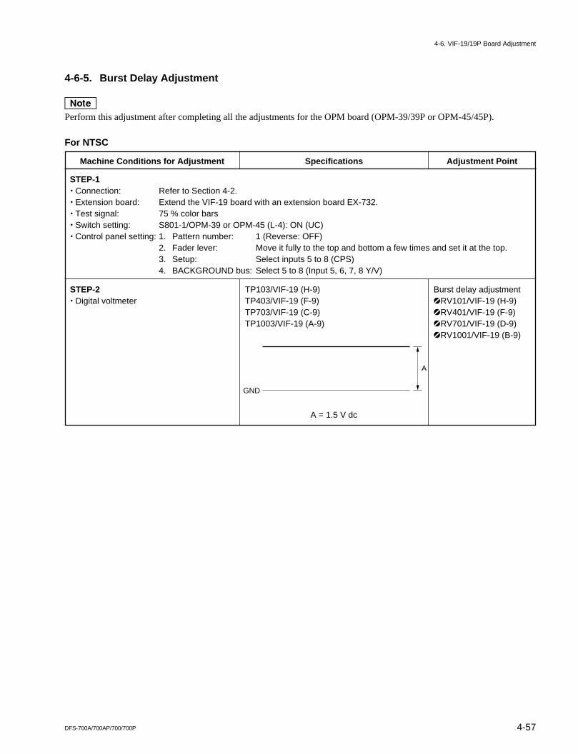
4-57DFS-700A/700AP/700/700P
4-6-5. Burst Delay Adjustment
nPerform this adjustment after completing all the adjustments for the OPM board (OPM-39/39P or OPM-45/45P).
For NTSC
Machine Conditions for Adjustment Specifications Adjustment Point
TP103/VIF-19 (H-9)TP403/VIF-19 (F-9)TP703/VIF-19 (C-9)TP1003/VIF-19 (A-9)
A = 1.5 V dc
Burst delay adjustment1RV101/VIF-19 (H-9)1RV401/VIF-19 (F-9)1RV701/VIF-19 (D-9)1RV1001/VIF-19 (B-9)
STEP-1. Connection: Refer to Section 4-2.. Extension board: Extend the VIF-19 board with an extension board EX-732.. Test signal: 75 % color bars. Switch setting: S801-1/OPM-39 or OPM-45 (L-4): ON (UC). Control panel setting: 1. Pattern number: 1 (Reverse: OFF)
2. Fader lever: Move it fully to the top and bottom a few times and set it at the top.3. Setup: Select inputs 5 to 8 (CPS)4. BACKGROUND bus: Select 5 to 8 (Input 5, 6, 7, 8 Y/V)
STEP-2. Digital voltmeter
A
GND
4-6. VIF-19/19P Board Adjustment
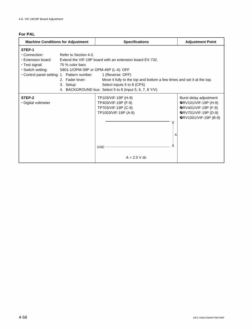
4-58 DFS-700A/700AP/700/700P
Machine Conditions for Adjustment Specifications Adjustment Point
TP103/VIF-19P (H-9)TP403/VIF-19P (F-9)TP703/VIF-19P (C-9)TP1003/VIF-19P (A-9)
A = 2.0 V dc
Burst delay adjustment1RV101/VIF-19P (H-9)1RV401/VIF-19P (F-9)1RV701/VIF-19P (D-9)1RV1001/VIF-19P (B-9)
STEP-1. Connection: Refer to Section 4-2.. Extension board: Extend the VIF-19P board with an extension board EX-732.. Test signal: 75 % color bars. Switch setting: S801-1/OPM-39P or OPM-45P (L-4): OFF. Control panel setting: 1. Pattern number: 1 (Reverse: OFF)
2. Fader lever: Move it fully to the top and bottom a few times and set it at the top.3. Setup: Select inputs 5 to 8 (CPS)4. BACKGROUND bus: Select 5 to 8 (Input 5, 6, 7, 8 Y/V)
STEP-2. Digital voltmeter
4-6. VIF-19/19P Board Adjustment
For PAL
A
GND
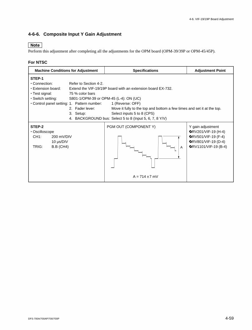
4-59DFS-700A/700AP/700/700P
4-6-6. Composite Input Y Gain Adjustment
nPerform this adjustment after completing all the adjustments for the OPM board (OPM-39/39P or OPM-45/45P).
For NTSC
Machine Conditions for Adjustment Specifications Adjustment Point
PGM OUT (COMPONENT Y)
A = 714 ±7 mV
Y gain adjustment1RV201/VIF-19 (H-4)1RV501/VIF-19 (F-4)1RV801/VIF-19 (D-4)1RV1101/VIF-19 (B-4)
STEP-1. Connection: Refer to Section 4-2.. Extension board: Extend the VIF-19/19P board with an extension board EX-732.. Test signal: 75 % color bars. Switch setting: S801-1/OPM-39 or OPM-45 (L-4): ON (UC). Control panel setting: 1. Pattern number: 1 (Reverse: OFF)
2. Fader lever: Move it fully to the top and bottom a few times and set it at the top.3. Setup: Select inputs 5 to 8 (CPS)4. BACKGROUND bus: Select 5 to 8 (Input 5, 6, 7, 8 Y/V)
STEP-2. Oscilloscope
CH1: 200 mV/DIV10 us/DIV
TRIG: B.B (CH4) A
4-6. VIF-19/19P Board Adjustment
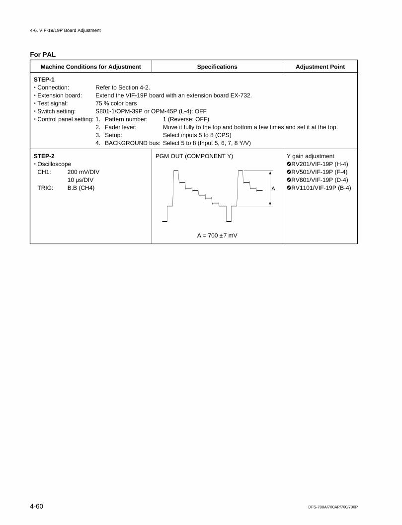
4-60 DFS-700A/700AP/700/700P
For PAL
Machine Conditions for Adjustment Specifications Adjustment Point
PGM OUT (COMPONENT Y)
A = 700 ±7 mV
Y gain adjustment1RV201/VIF-19P (H-4)1RV501/VIF-19P (F-4)1RV801/VIF-19P (D-4)1RV1101/VIF-19P (B-4)
STEP-1. Connection: Refer to Section 4-2.. Extension board: Extend the VIF-19P board with an extension board EX-732.. Test signal: 75 % color bars. Switch setting: S801-1/OPM-39P or OPM-45P (L-4): OFF. Control panel setting: 1. Pattern number: 1 (Reverse: OFF)
2. Fader lever: Move it fully to the top and bottom a few times and set it at the top.3. Setup: Select inputs 5 to 8 (CPS)4. BACKGROUND bus: Select 5 to 8 (Input 5, 6, 7, 8 Y/V)
STEP-2. Oscilloscope
CH1: 200 mV/DIV10 us/DIV
TRIG: B.B (CH4) A
4-6. VIF-19/19P Board Adjustment
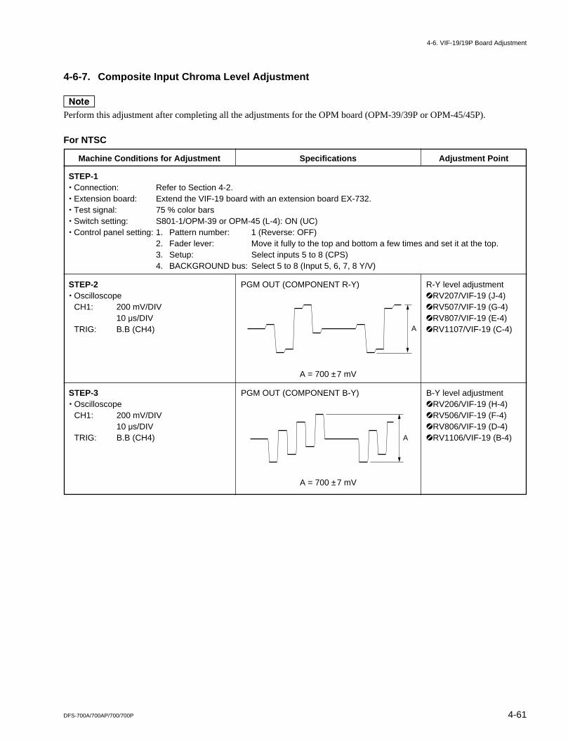
4-61DFS-700A/700AP/700/700P
4-6-7. Composite Input Chroma Level Adjustment
nPerform this adjustment after completing all the adjustments for the OPM board (OPM-39/39P or OPM-45/45P).
For NTSC
Machine Conditions for Adjustment Specifications Adjustment Point
PGM OUT (COMPONENT R-Y)
A = 700 ±7 mV
R-Y level adjustment1RV207/VIF-19 (J-4)1RV507/VIF-19 (G-4)1RV807/VIF-19 (E-4)1RV1107/VIF-19 (C-4)
STEP-1. Connection: Refer to Section 4-2.. Extension board: Extend the VIF-19 board with an extension board EX-732.. Test signal: 75 % color bars. Switch setting: S801-1/OPM-39 or OPM-45 (L-4): ON (UC). Control panel setting: 1. Pattern number: 1 (Reverse: OFF)
2. Fader lever: Move it fully to the top and bottom a few times and set it at the top.3. Setup: Select inputs 5 to 8 (CPS)4. BACKGROUND bus: Select 5 to 8 (Input 5, 6, 7, 8 Y/V)
STEP-2. Oscilloscope
CH1: 200 mV/DIV10 us/DIV
TRIG: B.B (CH4)
STEP-3. Oscilloscope
CH1: 200 mV/DIV10 us/DIV
TRIG: B.B (CH4)
PGM OUT (COMPONENT B-Y)
A = 700 ±7 mV
B-Y level adjustment1RV206/VIF-19 (H-4)1RV506/VIF-19 (F-4)1RV806/VIF-19 (D-4)1RV1106/VIF-19 (B-4)
A
A
4-6. VIF-19/19P Board Adjustment
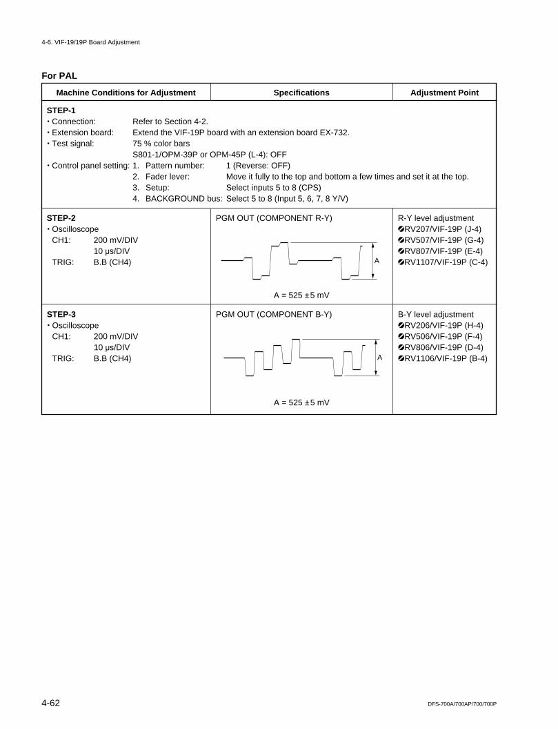
4-62 DFS-700A/700AP/700/700P
For PAL
Machine Conditions for Adjustment Specifications Adjustment Point
PGM OUT (COMPONENT R-Y)
A = 525 ±5 mV
R-Y level adjustment1RV207/VIF-19P (J-4)1RV507/VIF-19P (G-4)1RV807/VIF-19P (E-4)1RV1107/VIF-19P (C-4)
STEP-1. Connection: Refer to Section 4-2.. Extension board: Extend the VIF-19P board with an extension board EX-732.. Test signal: 75 % color bars
S801-1/OPM-39P or OPM-45P (L-4): OFF. Control panel setting: 1. Pattern number: 1 (Reverse: OFF)
2. Fader lever: Move it fully to the top and bottom a few times and set it at the top.3. Setup: Select inputs 5 to 8 (CPS)4. BACKGROUND bus: Select 5 to 8 (Input 5, 6, 7, 8 Y/V)
STEP-2. Oscilloscope
CH1: 200 mV/DIV10 us/DIV
TRIG: B.B (CH4)
STEP-3. Oscilloscope
CH1: 200 mV/DIV10 us/DIV
TRIG: B.B (CH4)
PGM OUT (COMPONENT B-Y)
A = 525 ±5 mV
B-Y level adjustment1RV206/VIF-19P (H-4)1RV506/VIF-19P (F-4)1RV806/VIF-19P (D-4)1RV1106/VIF-19P (B-4)
A
A
4-6. VIF-19/19P Board Adjustment

4-63DFS-700A/700AP/700/700P
4-6-8. S VIDEO Input Gain Adjustment
nPerform this adjustment after completing all the adjustments for the OPM board (OPM-39/39P or OPM-45/45P).
For NTSC
Machine Conditions for Adjustment Specifications Adjustment Point
PGM OUT (COMPONENT Y)
A = 714 ±7 mV
Y gain adjustment1RV103/VIF-19 (J-9)1RV403/VIF-19 (G-9)1RV703/VIF-19 (E-9)1RV1003/VIF-19 (C-9)
STEP-1. Connection: Refer to Section 4-2.. Extension board: Extend the VIF-19 board with an extension board EX-732.. Test signal: 75 % color bars. Switch setting: S801-1/OPM-39 or OPM-45 (L-4): ON (UC). Control panel setting: 1. Pattern number: 1 (Reverse: OFF)
2. Fader lever: Move it fully to the top and bottom a few times and set it at the top.3. Setup: Select inputs 5 to 8 (YC)4. BACKGROUND bus: Select 5 to 8 (Input 5, 6, 7, 8 S VIDEO)
STEP-2. Oscilloscope
CH1: 200 mV/DIV10 us/DIV
TRIG: B.B (CH4)A
4-6. VIF-19/19P Board Adjustment

4-64 DFS-700A/700AP/700/700P
For PAL
Machine Conditions for Adjustment Specifications Adjustment Point
PGM OUT (COMPONENT Y)
A = 700 ±7 mV
Y gain adjustment1RV103/VIF-19P (J-9)1RV403/VIF-19P (G-9)1RV703/VIF-19P (E-9)1RV1003/VIF-19P (C-9)
STEP-1. Connection: Refer to Section 4-2.. Extension board: Extend the VIF-19P board with an extension board EX-732.. Test signal: 75 % color bars
S801-1/OPM-39P or OPM-45P (L-4): OFF. Control panel setting: 1. Pattern number: 1 (Reverse: OFF)
2. Fader lever: Move it fully to the top and bottom a few times and set it at the top.3. Setup: Select inputs 5 to 8 (YC)4. BACKGROUND bus: Select 5 to 8 (Input 5, 6, 7, 8 S VIDEO)
STEP-2. Oscilloscope
CH1: 200 mV/DIV10 us/DIV
TRIG: B.B (CH4)A
4-6. VIF-19/19P Board Adjustment
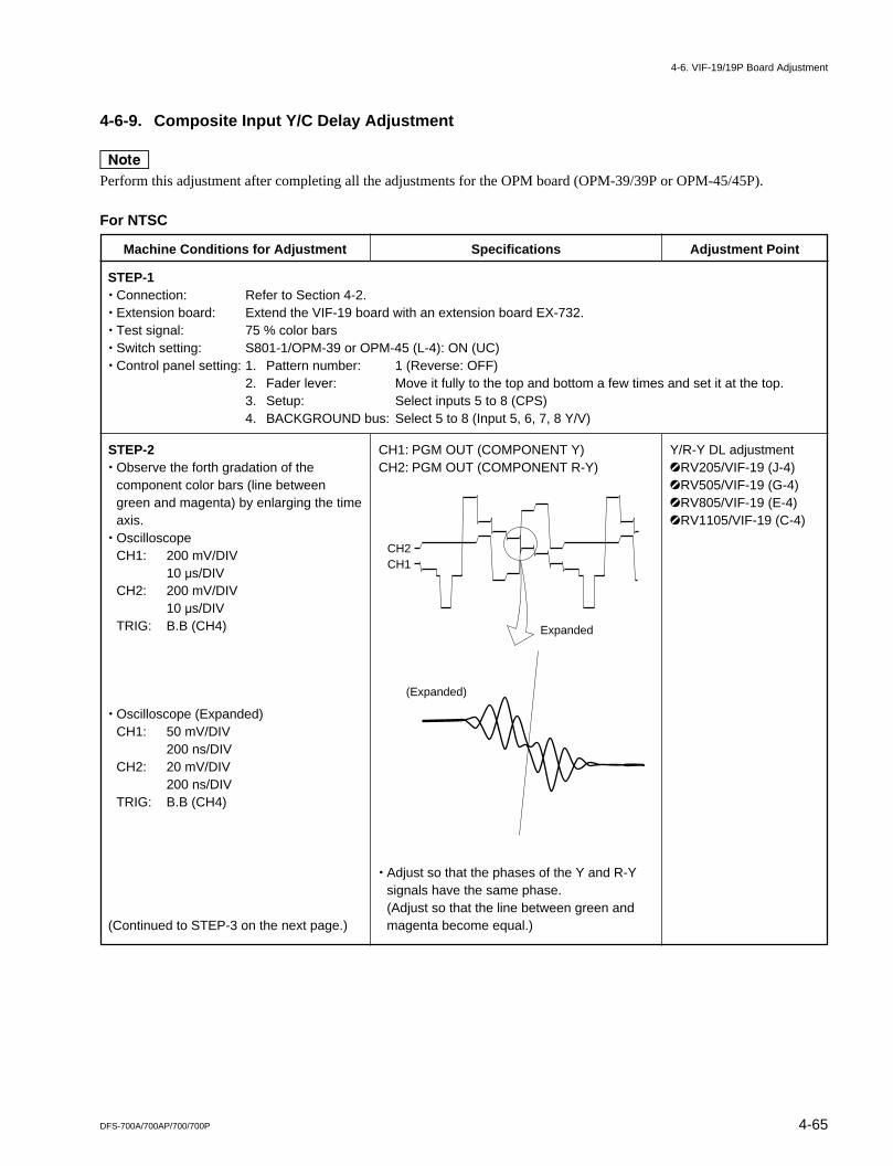
4-65DFS-700A/700AP/700/700P
4-6-9. Composite Input Y/C Delay Adjustment
nPerform this adjustment after completing all the adjustments for the OPM board (OPM-39/39P or OPM-45/45P).
For NTSC
Machine Conditions for Adjustment Specifications Adjustment Point
CH1: PGM OUT (COMPONENT Y)CH2: PGM OUT (COMPONENT R-Y)
. Adjust so that the phases of the Y and R-Ysignals have the same phase.(Adjust so that the line between green andmagenta become equal.)
Y/R-Y DL adjustment1RV205/VIF-19 (J-4)1RV505/VIF-19 (G-4)1RV805/VIF-19 (E-4)1RV1105/VIF-19 (C-4)
STEP-1. Connection: Refer to Section 4-2.. Extension board: Extend the VIF-19 board with an extension board EX-732.. Test signal: 75 % color bars. Switch setting: S801-1/OPM-39 or OPM-45 (L-4): ON (UC). Control panel setting: 1. Pattern number: 1 (Reverse: OFF)
2. Fader lever: Move it fully to the top and bottom a few times and set it at the top.3. Setup: Select inputs 5 to 8 (CPS)4. BACKGROUND bus: Select 5 to 8 (Input 5, 6, 7, 8 Y/V)
STEP-2. Observe the forth gradation of the
component color bars (line betweengreen and magenta) by enlarging the timeaxis.
. OscilloscopeCH1: 200 mV/DIV
10 us/DIVCH2: 200 mV/DIV
10 us/DIVTRIG: B.B (CH4)
. Oscilloscope (Expanded)CH1: 50 mV/DIV
200 ns/DIVCH2: 20 mV/DIV
200 ns/DIVTRIG: B.B (CH4)
(Continued to STEP-3 on the next page.)
(Expanded)
Expanded
CH2CH1
4-6. VIF-19/19P Board Adjustment

4-66 DFS-700A/700AP/700/700P
Machine Conditions for Adjustment Specifications Adjustment Point
CH1: PGM OUT (COMPONENT Y)CH2: PGM OUT (COMPONENT B-Y)
. Adjust so that the phases of the Y and B-Ysignals have the same phase.(Adjust so that the line between green andmagenta become equal.)
Y/B-Y DL adjustment1RV203/VIF-19 (J-4)1RV503/VIF-19 (G-4)1RV803/VIF-19 (D-4)1RV1103/VIF-19 (B-4)
STEP-3. Observe the forth gradation of the
component color bars (line betweengreen and magenta) by enlarging the timeaxis.
. OscilloscopeCH1: 200 mV/DIV
10 us/DIVCH2: 200 mV/DIV
10 us/DIVTRIG: B.B (CH4)
. Oscilloscope (Expanded)CH1: 50 mV/DIV
200 ns/DIVCH2: 20 mV/DIV
200 ns/DIVTRIG: B.B (CH4)
CH2
CH1
(Expanded)
Expanded
4-6. VIF-19/19P Board Adjustment
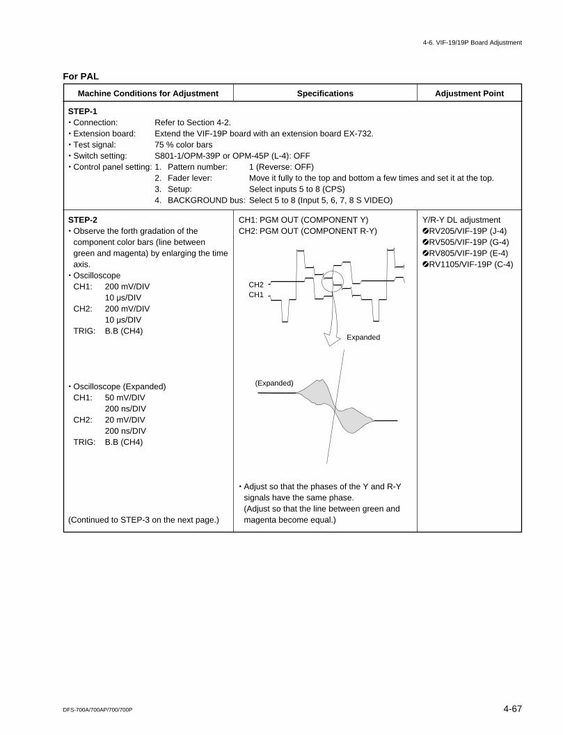
4-67DFS-700A/700AP/700/700P
For PAL
Machine Conditions for Adjustment Specifications Adjustment Point
CH1: PGM OUT (COMPONENT Y)CH2: PGM OUT (COMPONENT R-Y)
. Adjust so that the phases of the Y and R-Ysignals have the same phase.(Adjust so that the line between green andmagenta become equal.)
Y/R-Y DL adjustment1RV205/VIF-19P (J-4)1RV505/VIF-19P (G-4)1RV805/VIF-19P (E-4)1RV1105/VIF-19P (C-4)
STEP-1. Connection: Refer to Section 4-2.. Extension board: Extend the VIF-19P board with an extension board EX-732.. Test signal: 75 % color bars. Switch setting: S801-1/OPM-39P or OPM-45P (L-4): OFF. Control panel setting: 1. Pattern number: 1 (Reverse: OFF)
2. Fader lever: Move it fully to the top and bottom a few times and set it at the top.3. Setup: Select inputs 5 to 8 (CPS)4. BACKGROUND bus: Select 5 to 8 (Input 5, 6, 7, 8 S VIDEO)
STEP-2. Observe the forth gradation of the
component color bars (line betweengreen and magenta) by enlarging the timeaxis.
. OscilloscopeCH1: 200 mV/DIV
10 us/DIVCH2: 200 mV/DIV
10 us/DIVTRIG: B.B (CH4)
. Oscilloscope (Expanded)CH1: 50 mV/DIV
200 ns/DIVCH2: 20 mV/DIV
200 ns/DIVTRIG: B.B (CH4)
(Continued to STEP-3 on the next page.)
CH2CH1
Expanded
(Expanded)
4-6. VIF-19/19P Board Adjustment
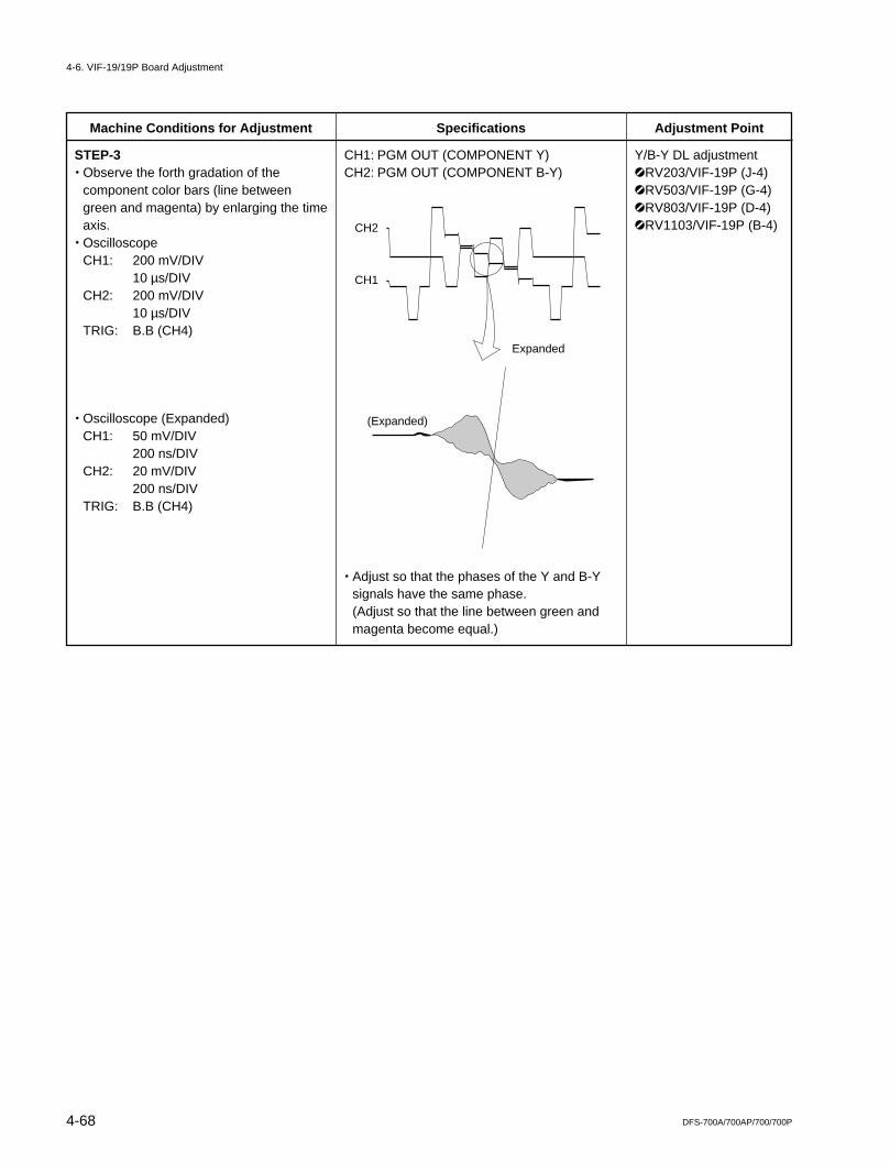
4-68 DFS-700A/700AP/700/700P
Machine Conditions for Adjustment Specifications Adjustment Point
CH1: PGM OUT (COMPONENT Y)CH2: PGM OUT (COMPONENT B-Y)
. Adjust so that the phases of the Y and B-Ysignals have the same phase.(Adjust so that the line between green andmagenta become equal.)
Y/B-Y DL adjustment1RV203/VIF-19P (J-4)1RV503/VIF-19P (G-4)1RV803/VIF-19P (D-4)1RV1103/VIF-19P (B-4)
STEP-3. Observe the forth gradation of the
component color bars (line betweengreen and magenta) by enlarging the timeaxis.
. OscilloscopeCH1: 200 mV/DIV
10 µs/DIVCH2: 200 mV/DIV
10 µs/DIVTRIG: B.B (CH4)
. Oscilloscope (Expanded)CH1: 50 mV/DIV
200 ns/DIVCH2: 20 mV/DIV
200 ns/DIVTRIG: B.B (CH4)
CH2
CH1
Expanded
(Expanded)
4-6. VIF-19/19P Board Adjustment
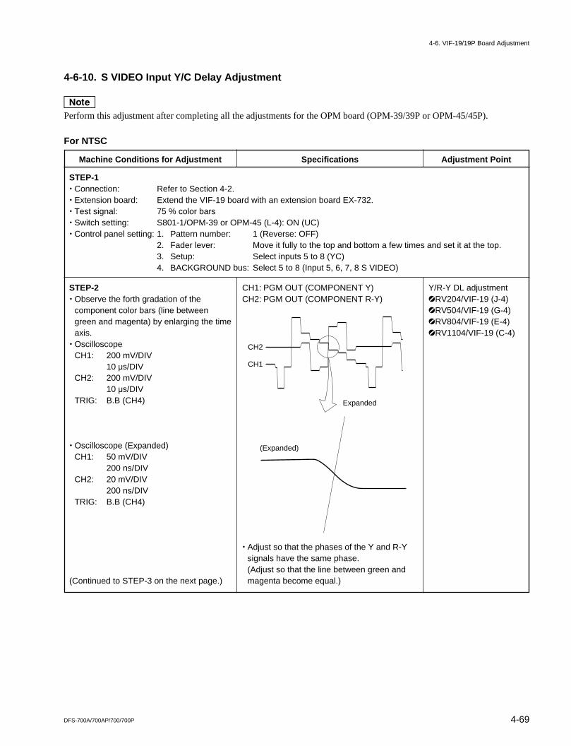
4-69DFS-700A/700AP/700/700P
4-6-10. S VIDEO Input Y/C Delay Adjustment
nPerform this adjustment after completing all the adjustments for the OPM board (OPM-39/39P or OPM-45/45P).
For NTSC
Machine Conditions for Adjustment Specifications Adjustment Point
CH1: PGM OUT (COMPONENT Y)CH2: PGM OUT (COMPONENT R-Y)
. Adjust so that the phases of the Y and R-Ysignals have the same phase.(Adjust so that the line between green andmagenta become equal.)
Y/R-Y DL adjustment1RV204/VIF-19 (J-4)1RV504/VIF-19 (G-4)1RV804/VIF-19 (E-4)1RV1104/VIF-19 (C-4)
STEP-1. Connection: Refer to Section 4-2.. Extension board: Extend the VIF-19 board with an extension board EX-732.. Test signal: 75 % color bars. Switch setting: S801-1/OPM-39 or OPM-45 (L-4): ON (UC). Control panel setting: 1. Pattern number: 1 (Reverse: OFF)
2. Fader lever: Move it fully to the top and bottom a few times and set it at the top.3. Setup: Select inputs 5 to 8 (YC)4. BACKGROUND bus: Select 5 to 8 (Input 5, 6, 7, 8 S VIDEO)
STEP-2. Observe the forth gradation of the
component color bars (line betweengreen and magenta) by enlarging the timeaxis.
. OscilloscopeCH1: 200 mV/DIV
10 us/DIVCH2: 200 mV/DIV
10 us/DIVTRIG: B.B (CH4)
. Oscilloscope (Expanded)CH1: 50 mV/DIV
200 ns/DIVCH2: 20 mV/DIV
200 ns/DIVTRIG: B.B (CH4)
(Continued to STEP-3 on the next page.)
CH2
CH1
Expanded
(Expanded)
4-6. VIF-19/19P Board Adjustment

4-70 DFS-700A/700AP/700/700P
Machine Conditions for Adjustment Specifications Adjustment Point
CH1: PGM OUT (COMPONENT Y)CH2: PGM OUT (COMPONENT B-Y)
. Adjust so that the phases of the Y and B-Ysignals have the same phase.(Adjust so that the line between green andmagenta become equal.)
Y/B-Y DL adjustment1RV202/VIF-19 (J-4)1RV502/VIF-19 (G-4)1RV802/VIF-19 (D-4)1RV1102/VIF-19 (B-4)
STEP-3. Observe the forth gradation of the
component color bars (line betweengreen and magenta) by enlarging the timeaxis.
. OscilloscopeCH1: 200 mV/DIV
10 us/DIVCH2: 200 mV/DIV
10 us/DIVTRIG: B.B (CH4)
. Oscilloscope (Expanded)CH1: 50 mV/DIV
200 ns/DIVCH2: 20 mV/DIV
200 ns/DIVTRIG: B.B (CH4)
CH2
CH1
Expanded
(Expanded)
4-6. VIF-19/19P Board Adjustment
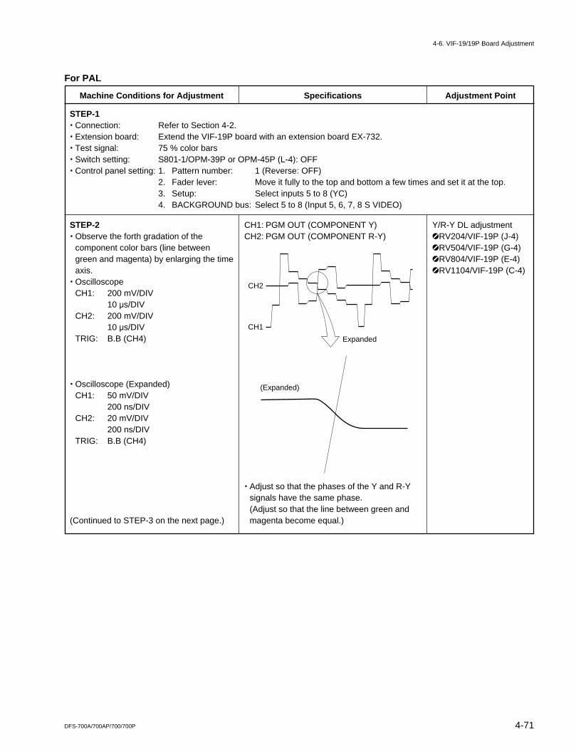
4-71DFS-700A/700AP/700/700P
For PAL
Machine Conditions for Adjustment Specifications Adjustment Point
CH1: PGM OUT (COMPONENT Y)CH2: PGM OUT (COMPONENT R-Y)
. Adjust so that the phases of the Y and R-Ysignals have the same phase.(Adjust so that the line between green andmagenta become equal.)
Y/R-Y DL adjustment1RV204/VIF-19P (J-4)1RV504/VIF-19P (G-4)1RV804/VIF-19P (E-4)1RV1104/VIF-19P (C-4)
STEP-1. Connection: Refer to Section 4-2.. Extension board: Extend the VIF-19P board with an extension board EX-732.. Test signal: 75 % color bars. Switch setting: S801-1/OPM-39P or OPM-45P (L-4): OFF. Control panel setting: 1. Pattern number: 1 (Reverse: OFF)
2. Fader lever: Move it fully to the top and bottom a few times and set it at the top.3. Setup: Select inputs 5 to 8 (YC)4. BACKGROUND bus: Select 5 to 8 (Input 5, 6, 7, 8 S VIDEO)
STEP-2. Observe the forth gradation of the
component color bars (line betweengreen and magenta) by enlarging the timeaxis.
. OscilloscopeCH1: 200 mV/DIV
10 us/DIVCH2: 200 mV/DIV
10 us/DIVTRIG: B.B (CH4)
. Oscilloscope (Expanded)CH1: 50 mV/DIV
200 ns/DIVCH2: 20 mV/DIV
200 ns/DIVTRIG: B.B (CH4)
(Continued to STEP-3 on the next page.)
CH2
CH1
Expanded
(Expanded)
4-6. VIF-19/19P Board Adjustment
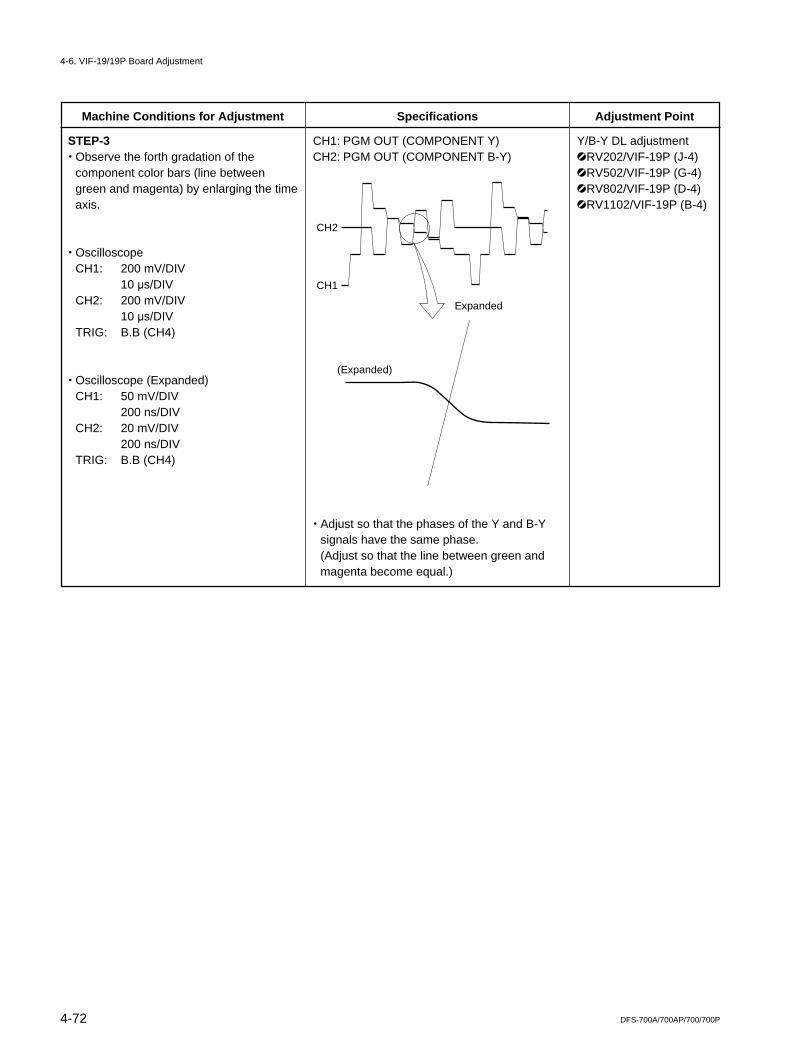
4-72 DFS-700A/700AP/700/700P
Machine Conditions for Adjustment Specifications Adjustment Point
CH1: PGM OUT (COMPONENT Y)CH2: PGM OUT (COMPONENT B-Y)
. Adjust so that the phases of the Y and B-Ysignals have the same phase.(Adjust so that the line between green andmagenta become equal.)
Y/B-Y DL adjustment1RV202/VIF-19P (J-4)1RV502/VIF-19P (G-4)1RV802/VIF-19P (D-4)1RV1102/VIF-19P (B-4)
STEP-3. Observe the forth gradation of the
component color bars (line betweengreen and magenta) by enlarging the timeaxis.
. OscilloscopeCH1: 200 mV/DIV
10 us/DIVCH2: 200 mV/DIV
10 us/DIVTRIG: B.B (CH4)
. Oscilloscope (Expanded)CH1: 50 mV/DIV
200 ns/DIVCH2: 20 mV/DIV
200 ns/DIVTRIG: B.B (CH4)
CH2
CH1
Expanded
(Expanded)
4-6. VIF-19/19P Board Adjustment
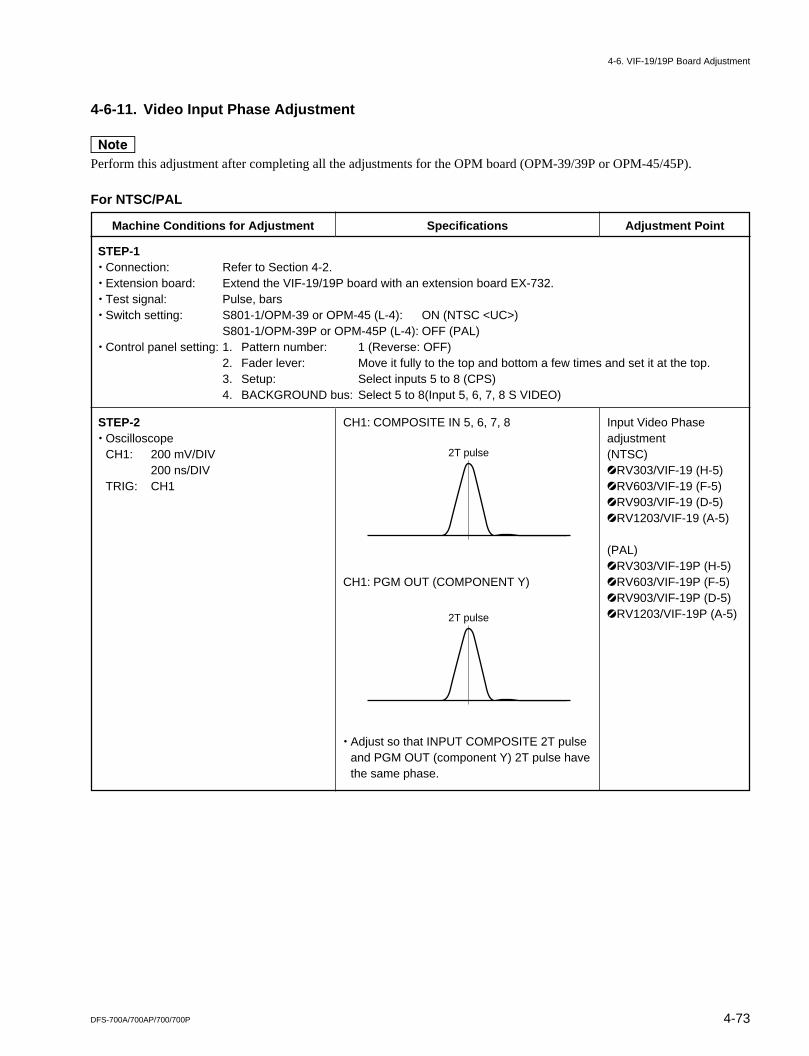
4-73DFS-700A/700AP/700/700P
4-6-11. Video Input Phase Adjustment
nPerform this adjustment after completing all the adjustments for the OPM board (OPM-39/39P or OPM-45/45P).
For NTSC/PAL
Machine Conditions for Adjustment Specifications Adjustment Point
CH1: COMPOSITE IN 5, 6, 7, 8
CH1: PGM OUT (COMPONENT Y)
. Adjust so that INPUT COMPOSITE 2T pulseand PGM OUT (component Y) 2T pulse havethe same phase.
Input Video Phaseadjustment(NTSC)1RV303/VIF-19 (H-5)1RV603/VIF-19 (F-5)1RV903/VIF-19 (D-5)1RV1203/VIF-19 (A-5)
(PAL)1RV303/VIF-19P (H-5)1RV603/VIF-19P (F-5)1RV903/VIF-19P (D-5)1RV1203/VIF-19P (A-5)
STEP-1. Connection: Refer to Section 4-2.. Extension board: Extend the VIF-19/19P board with an extension board EX-732.. Test signal: Pulse, bars. Switch setting: S801-1/OPM-39 or OPM-45 (L-4): ON (NTSC <UC>)
S801-1/OPM-39P or OPM-45P (L-4): OFF (PAL). Control panel setting: 1. Pattern number: 1 (Reverse: OFF)
2. Fader lever: Move it fully to the top and bottom a few times and set it at the top.3. Setup: Select inputs 5 to 8 (CPS)4. BACKGROUND bus: Select 5 to 8(Input 5, 6, 7, 8 S VIDEO)
STEP-2. Oscilloscope
CH1: 200 mV/DIV200 ns/DIV
TRIG: CH1
2T pulse
2T pulse
4-6. VIF-19/19P Board Adjustment
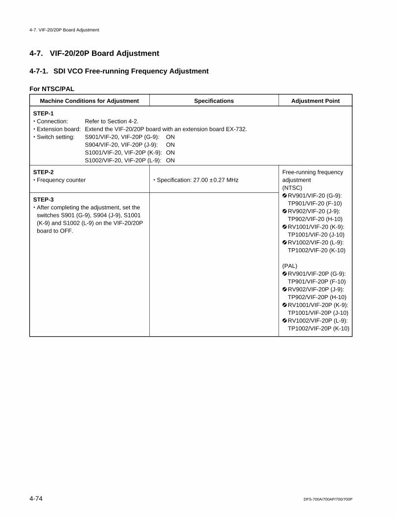
4-74 DFS-700A/700AP/700/700P
Machine Conditions for Adjustment Specifications Adjustment Point
. Specification: 27.00 ±0.27 MHzFree-running frequencyadjustment(NTSC)1 RV901/VIF-20 (G-9):
TP901/VIF-20 (F-10)1 RV902/VIF-20 (J-9):
TP902/VIF-20 (H-10)1 RV1001/VIF-20 (K-9):
TP1001/VIF-20 (J-10)1 RV1002/VIF-20 (L-9):
TP1002/VIF-20 (K-10)
(PAL)1 RV901/VIF-20P (G-9):
TP901/VIF-20P (F-10)1 RV902/VIF-20P (J-9):
TP902/VIF-20P (H-10)1 RV1001/VIF-20P (K-9):
TP1001/VIF-20P (J-10)1 RV1002/VIF-20P (L-9):
TP1002/VIF-20P (K-10)
STEP-1. Connection: Refer to Section 4-2.. Extension board: Extend the VIF-20/20P board with an extension board EX-732.. Switch setting: S901/VIF-20, VIF-20P (G-9): ON
S904/VIF-20, VIF-20P (J-9): ONS1001/VIF-20, VIF-20P (K-9): ONS1002/VIF-20, VIF-20P (L-9): ON
STEP-2. Frequency counter
STEP-3. After completing the adjustment, set the
switches S901 (G-9), S904 (J-9), S1001(K-9) and S1002 (L-9) on the VIF-20/20Pboard to OFF.
4-7. VIF-20/20P Board Adjustment
4-7-1. SDI VCO Free-running Frequency Adjustment
For NTSC/PAL
4-7. VIF-20/20P Board Adjustment
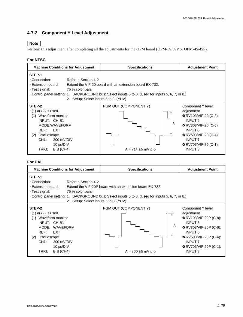
4-75DFS-700A/700AP/700/700P
4-7-2. Component Y Level Adjustment
nPerform this adjustment after completing all the adjustments for the OPM board (OPM-39/39P or OPM-45/45P).
For NTSC
Machine Conditions for Adjustment Specifications Adjustment Point
PGM OUT (COMPONENT Y)
A = 714 ±5 mV p-p
Component Y leveladjustment1 RV103/VIF-20 (C-8):
INPUT 51 RV303/VIF-20 (C-6):
INPUT 61 RV503/VIF-20 (C-4):
INPUT 71 RV703/VIF-20 (C-1):
INPUT 8
STEP-1. Connection: Refer to Section 4-2. Extension board: Extend the VIF-20 board with an extension board EX-732.. Test signal: 75 % color bars. Control panel setting: 1. BACKGROUND bus: Select inputs 5 to 8. (Used for inputs 5, 6, 7, or 8.)
2. Setup: Select inputs 5 to 8. (YUV)
STEP-2. (1) or (2) is used.
(1) Waveform monitorINPUT: CH-B1MODE:WAVEFORMREF: EXT
(2) OscilloscopeCH1: 200 mV/DIV
10 us/DIVTRIG: B.B (CH4)
A
For PAL
Machine Conditions for Adjustment Specifications Adjustment Point
PGM OUT (COMPONENT Y)
A = 700 ±5 mV p-p
Component Y leveladjustment1 RV103/VIF-20P (C-8):
INPUT 51 RV303/VIF-20P (C-6):
INPUT 61 RV503/VIF-20P (C-4):
INPUT 71 RV703/VIF-20P (C-1):
INPUT 8
STEP-1. Connection: Refer to Section 4-2.. Extension board: Extend the VIF-20P board with an extension board EX-732.. Test signal: 75 % color bars. Control panel setting: 1. BACKGROUND bus: Select inputs 5 to 8. (Used for inputs 5, 6, 7, or 8.)
2. Setup: Select inputs 5 to 8. (YUV)
STEP-2. (1) or (2) is used.
(1) Waveform monitorINPUT: CH-B1MODE: WAVEFORMREF: EXT
(2) OscilloscopeCH1: 200 mV/DIV
10 us/DIVTRIG: B.B (CH4)
A
4-7. VIF-20/20P Board Adjustment
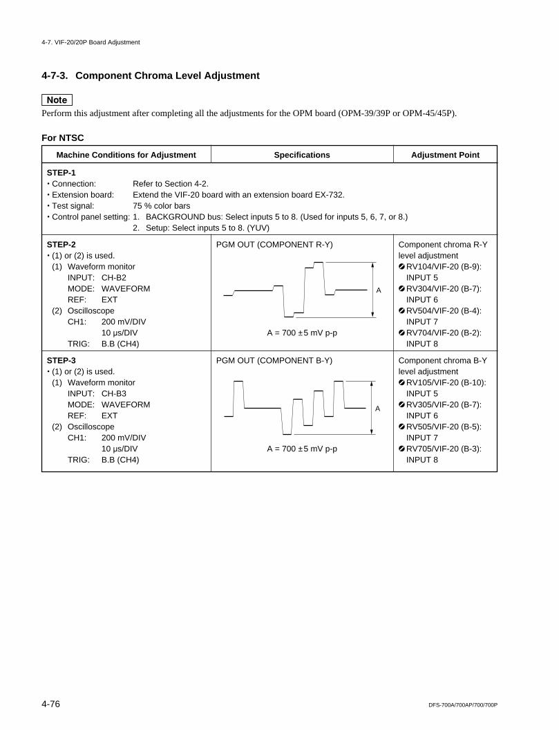
4-76 DFS-700A/700AP/700/700P
4-7-3. Component Chroma Level Adjustment
nPerform this adjustment after completing all the adjustments for the OPM board (OPM-39/39P or OPM-45/45P).
For NTSC
Machine Conditions for Adjustment Specifications Adjustment Point
PGM OUT (COMPONENT R-Y)
A = 700 ±5 mV p-p
PGM OUT (COMPONENT B-Y)
A = 700 ±5 mV p-p
Component chroma R-Ylevel adjustment1 RV104/VIF-20 (B-9):
INPUT 51 RV304/VIF-20 (B-7):
INPUT 61 RV504/VIF-20 (B-4):
INPUT 71 RV704/VIF-20 (B-2):
INPUT 8
Component chroma B-Ylevel adjustment1 RV105/VIF-20 (B-10):
INPUT 51 RV305/VIF-20 (B-7):
INPUT 61 RV505/VIF-20 (B-5):
INPUT 71 RV705/VIF-20 (B-3):
INPUT 8
STEP-1. Connection: Refer to Section 4-2.. Extension board: Extend the VIF-20 board with an extension board EX-732.. Test signal: 75 % color bars. Control panel setting: 1. BACKGROUND bus: Select inputs 5 to 8. (Used for inputs 5, 6, 7, or 8.)
2. Setup: Select inputs 5 to 8. (YUV)
STEP-2. (1) or (2) is used.
(1) Waveform monitorINPUT: CH-B2MODE: WAVEFORMREF: EXT
(2) OscilloscopeCH1: 200 mV/DIV
10 us/DIVTRIG: B.B (CH4)
STEP-3. (1) or (2) is used.
(1) Waveform monitorINPUT: CH-B3MODE: WAVEFORMREF: EXT
(2) OscilloscopeCH1: 200 mV/DIV
10 us/DIVTRIG: B.B (CH4)
A
A
4-7. VIF-20/20P Board Adjustment
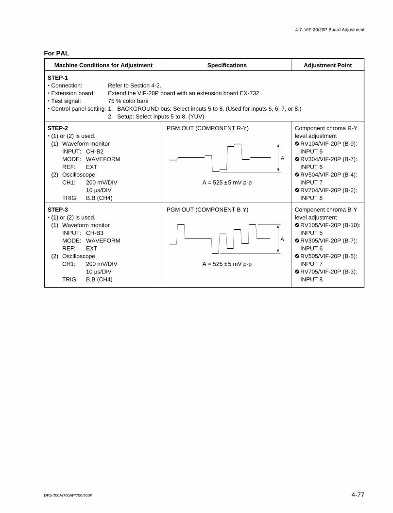
4-77DFS-700A/700AP/700/700P
For PAL
Machine Conditions for Adjustment Specifications Adjustment Point
PGM OUT (COMPONENT R-Y)
A = 525 ±5 mV p-p
PGM OUT (COMPONENT B-Y)
A = 525 ±5 mV p-p
Component chroma R-Ylevel adjustment1 RV104/VIF-20P (B-9):
INPUT 51 RV304/VIF-20P (B-7):
INPUT 61 RV504/VIF-20P (B-4):
INPUT 71 RV704/VIF-20P (B-2):
INPUT 8
Component chroma B-Ylevel adjustment1 RV105/VIF-20P (B-10):
INPUT 51 RV305/VIF-20P (B-7):
INPUT 61 RV505/VIF-20P (B-5):
INPUT 71 RV705/VIF-20P (B-3):
INPUT 8
STEP-1. Connection: Refer to Section 4-2.. Extension board: Extend the VIF-20P board with an extension board EX-732.. Test signal: 75 % color bars. Control panel setting: 1. BACKGROUND bus: Select inputs 5 to 8. (Used for inputs 5, 6, 7, or 8.)
2. Setup: Select inputs 5 to 8. (YUV)
STEP-2. (1) or (2) is used.
(1) Waveform monitorINPUT: CH-B2MODE: WAVEFORMREF: EXT
(2) OscilloscopeCH1: 200 mV/DIV
10 us/DIVTRIG: B.B (CH4)
STEP-3. (1) or (2) is used.
(1) Waveform monitorINPUT: CH-B3MODE: WAVEFORMREF: EXT
(2) OscilloscopeCH1: 200 mV/DIV
10 us/DIVTRIG: B.B (CH4)
A
A
4-7. VIF-20/20P Board Adjustment
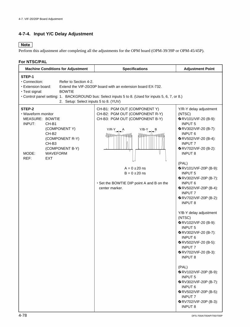
4-78 DFS-700A/700AP/700/700P
4-7-4. Input Y/C Delay Adjustment
nPerform this adjustment after completing all the adjustments for the OPM board (OPM-39/39P or OPM-45/45P).
For NTSC/PAL
Machine Conditions for Adjustment Specifications Adjustment Point
CH-B1: PGM OUT (COMPONENT Y)CH-B2: PGM OUT (COMPONENT R-Y)CH-B3: PGM OUT (COMPONENT B-Y)
A = 0 ±20 nsB = 0 ±20 ns
. Set the BOWTIE DIP point A and B on thecenter marker.
Y/R-Y delay adjustment(NTSC)1 RV101/VIF-20 (B-9):
INPUT 51 RV302/VIF-20 (B-7):
INPUT 61 RV502/VIF-20 (B-4):
INPUT 71 RV702/VIF-20 (B-2):
INPUT 8
(PAL)1 RV101/VIF-20P (B-9):
INPUT 51 RV302/VIF-20P (B-7):
INPUT 61 RV502/VIF-20P (B-4):
INPUT 71 RV702/VIF-20P (B-2):
INPUT 8
Y/B-Y delay adjustment(NTSC)1 RV102/VIF-20 (B-9):
INPUT 51 RV302/VIF-20 (B-7):
INPUT 61 RV502/VIF-20 (B-5):
INPUT 71 RV702/VIF-20 (B-3):
INPUT 8
(PAL)1 RV102/VIF-20P (B-9):
INPUT 51 RV302/VIF-20P (B-7):
INPUT 61 RV502/VIF-20P (B-5):
INPUT 71 RV702/VIF-20P (B-3):
INPUT 8
STEP-1. Connection: Refer to Section 4-2.. Extension board: Extend the VIF-20/20P board with an extension board EX-732.. Test signal: BOWTIE. Control panel setting: 1. BACKGROUND bus: Select inputs 5 to 8. (Used for inputs 5, 6, 7, or 8.)
2. Setup: Select inputs 5 to 8. (YUV)
STEP-2. Waveform monitor
MEASURE: BOWTIEINPUT: CH-B1
(COMPONENT Y)CH-B2(COMPONENT R-Y)CH-B3(COMPONENT B-Y)
MODE: WAVEFORMREF: EXT
AY/R-Y BY/B-Y
4-7. VIF-20/20P Board Adjustment
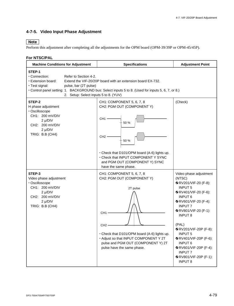
4-79DFS-700A/700AP/700/700P
4-7-5. Video Input Phase Adjustment
nPerform this adjustment after completing all the adjustments for the OPM board (OPM-39/39P or OPM-45/45P).
For NTSC/PAL
Machine Conditions for Adjustment Specifications Adjustment Point
CH1: COMPONENT 5, 6, 7, 8CH2: PGM OUT (COMPONENT Y)
. Check that D101/OPM board (A-6) lights up.
. Check that INPUT COMPONENT Y SYNCand PGM OUT (COMPONENT Y) SYNChave the same phase.
CH1: COMPONENT 5, 6, 7, 8CH2: PGM OUT (COMPONENT Y)
. Check that D101/OPM board (A-6) lights up.
. Adjust so that INPUT COMPONENT Y 2Tpulse and PGM OUT (COMPONENT Y) 2Tpulse have the same phase.
(Check)
Video phase adjustment(NTSC)1 RV201/VIF-20 (F-8):
INPUT 51 RV401/VIF-20 (F-6):
INPUT 61 RV601/VIF-20 (F-4):
INPUT 71 RV801/VIF-20 (F-1):
INPUT 8
(PAL)1 RV201/VIF-20P (F-8):
INPUT 51 RV401/VIF-20P (F-6):
INPUT 61 RV601/VIF-20P (F-4):
INPUT 71 RV801/VIF-20P (F-1):
INPUT 8
STEP-1. Connection: Refer to Section 4-2.. Extension board: Extend the VIF-20/20P board with an extension board EX-732.. Test signal: pulse, bar (2T pulse). Control panel setting: 1. BACKGROUND bus: Select inputs 5 to 8. (Used for inputs 5, 6, 7, or 8.)
2. Setup: Select inputs 5 to 8. (YUV)
STEP-2H phase adjustment. Oscilloscope
CH1: 200 mV/DIV2 u/DIV
CH2: 200 mV/DIV2 u/DIV
TRIG: B.B (CH4)
STEP-3Video phase adjustment. Oscilloscope
CH1: 200 mV/DIV2 u/DIV
CH2: 200 mV/DIV2 u/DIV
TRIG: B.B (CH4)
CH1
CH2
50 %
50 %
2T pulse
CH1
CH2
4-7. VIF-20/20P Board Adjustment
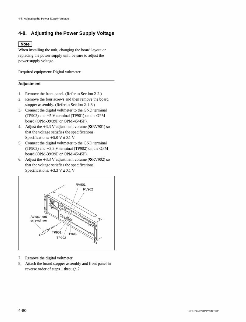
4-80 DFS-700A/700AP/700/700P
4-8. Adjusting the Power Supply Voltage
nWhen installing the unit, changing the board layout orreplacing the power supply unit, be sure to adjust thepower supply voltage.
Required equipment:Digital voltmeter
Adjustment
1. Remove the front panel. (Refer to Section 2-2.)2. Remove the four screws and then remove the board
stopper assembly. (Refer to Section 2-1-8.)3. Connect the digital voltmeter to the GND terminal
(TP903) and +5 V terminal (TP901) on the OPMboard (OPM-39/39P or OPM-45/45P).
4. Adjust the +3.3 V adjustment volume (1RV901) sothat the voltage satisfies the specifications.Specifications: +5.0 V ±0.1 V
5. Connect the digital voltmeter to the GND terminal(TP903) and +3.3 V terminal (TP902) on the OPMboard (OPM-39/39P or OPM-45/45P).
6. Adjust the +3.3 V adjustment volume (1RV902) sothat the voltage satisfies the specifications.Specifications: +3.3 V ±0.1 V
7. Remove the digital voltmeter.8. Attach the board stopper assembly and front panel in
reverse order of steps 1 through 2.
4-8. Adjusting the Power Supply Voltage
RV901
RV902
TP901
Adjustmentscrewdriver
TP902TP903
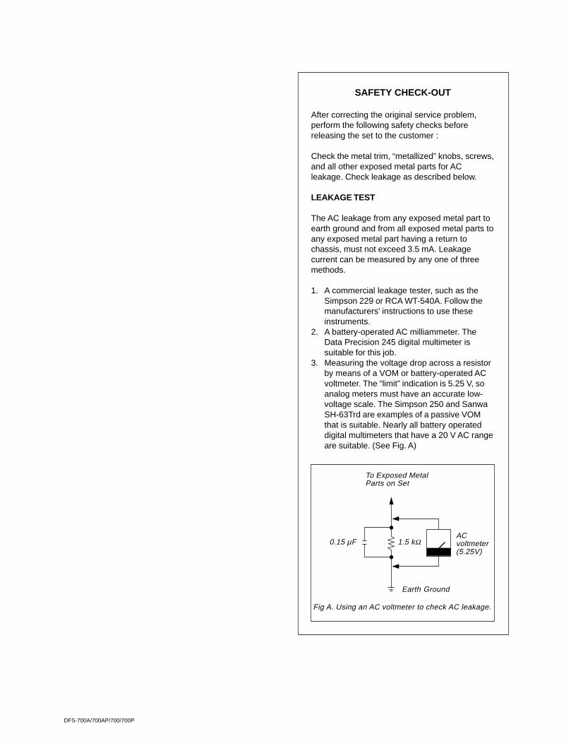
DFS-700A/700AP/700/700P
SAFETY CHECK-OUT
After correcting the original service problem,perform the following safety checks beforereleasing the set to the customer :
Check the metal trim, “metallized” knobs, screws,and all other exposed metal parts for ACleakage. Check leakage as described below.
LEAKAGE TEST
The AC leakage from any exposed metal part toearth ground and from all exposed metal parts toany exposed metal part having a return tochassis, must not exceed 3.5 mA. Leakagecurrent can be measured by any one of threemethods.
1. A commercial leakage tester, such as theSimpson 229 or RCA WT-540A. Follow themanufacturers’ instructions to use theseinstruments.
2. A battery-operated AC milliammeter. TheData Precision 245 digital multimeter issuitable for this job.
3. Measuring the voltage drop across a resistorby means of a VOM or battery-operated ACvoltmeter. The “limit” indication is 5.25 V, soanalog meters must have an accurate low-voltage scale. The Simpson 250 and SanwaSH-63Trd are examples of a passive VOMthat is suitable. Nearly all battery operateddigital multimeters that have a 20 V AC rangeare suitable. (See Fig. A)
To Exposed MetalParts on Set
Fig A. Using an AC voltmeter to check AC leakage.
ACvoltmeter(5.25V)
Earth Ground
0.15 µF 1.5 kZ

Printed in Japan
Sony Corporation 2003. 1 22
B&P Company ©2000
DFS-700A (UC)
DFS-700AP (CE)
DFS-700 (UC)
DFS-700P (CE) E
9-967-897-03