Embed Size (px)
Citation preview
Dr. Babasaheb Ambedkar Technological University
Course Structure and Syllabus
For
M. Tech. (VLSI)
Two Year (Four Semester) Course
(w.e.f. July 2017)
DR. BABASAHEB AMBEDKAR TECHNOLOGICAL UNIVERSITY,
Lonere-402103, Raigad (MS)
1
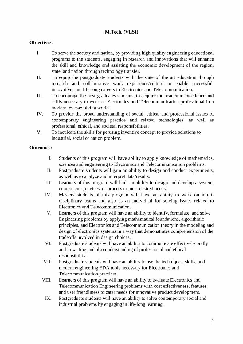
M.Tech. (VLSI)
Objectives:
I. To serve the society and nation, by providing high quality engineering educational
programs to the students, engaging in research and innovations that will enhance
the skill and knowledge and assisting the economic development of the region,
state, and nation through technology transfer.
II. To equip the postgraduate students with the state of the art education through
research and collaborative work experience/culture to enable successful,
innovative, and life-long careers in Electronics and Telecommunication.
III. To encourage the post-graduates students, to acquire the academic excellence and
skills necessary to work as Electronics and Telecommunication professional in a
modern, ever-evolving world.
IV. To provide the broad understanding of social, ethical and professional issues of
contemporary engineering practice and related technologies, as well as
professional, ethical, and societal responsibilities.
V. To inculcate the skills for perusing inventive concept to provide solutions to
industrial, social or nation problem.
Outcomes:
I. Students of this program will have ability to apply knowledge of mathematics,
sciences and engineering to Electronics and Telecommunication problems.
II. Postgraduate students will gain an ability to design and conduct experiments,
as well as to analyze and interpret data/results.
III. Learners of this program will built an ability to design and develop a system,
components, devices, or process to meet desired needs.
IV. Masters students of this program will have an ability to work on multi-
disciplinary teams and also as an individual for solving issues related to
Electronics and Telecommunication.
V. Learners of this program will have an ability to identify, formulate, and solve
Engineering problems by applying mathematical foundations, algorithmic
principles, and Electronics and Telecommunication theory in the modeling and
design of electronics systems in a way that demonstrates comprehension of the
tradeoffs involved in design choices.
VI. Postgraduate students will have an ability to communicate effectively orally
and in writing and also understanding of professional and ethical
responsibility.
VII. Postgraduate students will have an ability to use the techniques, skills, and
modern engineering EDA tools necessary for Electronics and
Telecommunication practices.
VIII. Learners of this program will have an ability to evaluate Electronics and
Telecommunication Engineering problems with cost effectiveness, features,
and user friendliness to cater needs for innovative product development.
IX. Postgraduate students will have an ability to solve contemporary social and
industrial problems by engaging in life-long learning.
2
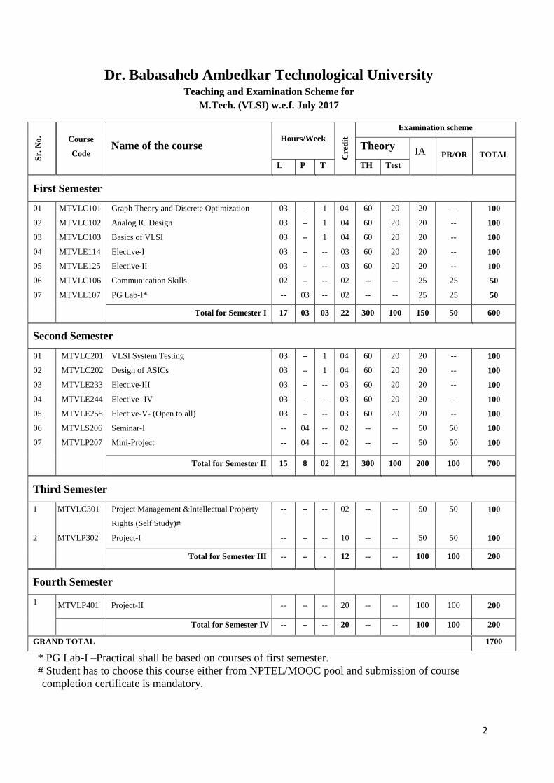
Dr. Babasaheb Ambedkar Technological University Teaching and Examination Scheme for
M.Tech. (VLSI) w.e.f. July 2017
Sr.
No
.
Course
Code Name of the course
Hours/Week
Cre
dit
Examination scheme
Theory IA PR/OR TOTAL
L P T TH Test
First Semester
01
02
03
04
05
06
07
MTVLC101
MTVLC102
MTVLC103
MTVLE114
MTVLE125
MTVLC106
MTVLL107
Graph Theory and Discrete Optimization
Analog IC Design
Basics of VLSI
Elective-I
Elective-II
Communication Skills
PG Lab-I*
03
03
03
03
03
02
--
--
--
--
--
--
--
03
1
1
1
--
--
--
--
04
04
04
03
03
02
02
60
60
60
60
60
--
--
20
20
20
20
20
--
--
20
20
20
20
20
25
25
--
--
--
--
--
25
25
100
100
100
100
100
50
50
Total for Semester I 17 03 03 22 300 100 150 50 600
Second Semester
01
02
03
04
05
06
07
MTVLC201
MTVLC202
MTVLE233
MTVLE244
MTVLE255
MTVLS206
MTVLP207
VLSI System Testing
Design of ASICs
Elective-III
Elective- IV
Elective-V- (Open to all)
Seminar-I
Mini-Project
03
03
03
03
03
--
--
--
--
--
--
--
04
04
1
1
--
--
--
--
--
04
04
03
03
03
02
02
60
60
60
60
60
--
--
20
20
20
20
20
--
--
20
20
20
20
20
50
50
--
--
--
--
--
50
50
100
100
100
100
100
100
100
Total for Semester II 15 8 02 21 300 100 200 100 700
Third Semester
1
2
MTVLC301
MTVLP302
Project Management &Intellectual Property
Rights (Self Study)#
Project-I
--
--
--
--
--
--
02
10
--
--
--
--
50
50
50
50
100
100
Total for Semester III -- -- - 12 -- -- 100 100 200
Fourth Semester
1
MTVLP401 Project-II -- -- -- 20 -- -- 100 100 200
Total for Semester IV -- -- -- 20 -- -- 100 100 200
GRAND TOTAL 1700
* PG Lab-I –Practical shall be based on courses of first semester.
# Student has to choose this course either from NPTEL/MOOC pool and submission of course
completion certificate is mandatory.
3
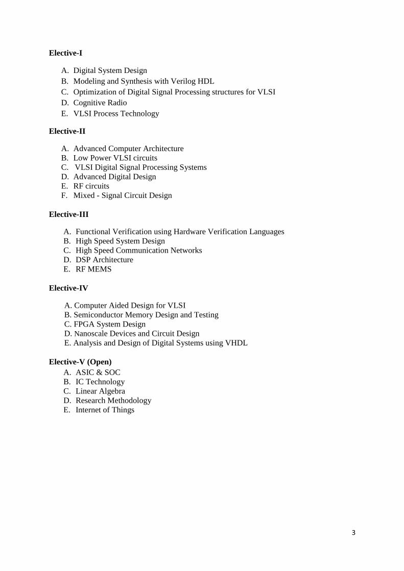
Elective-I
A. Digital System Design
B. Modeling and Synthesis with Verilog HDL
C. Optimization of Digital Signal Processing structures for VLSI
D. Cognitive Radio
E. VLSI Process Technology
Elective-II
A. Advanced Computer Architecture
B. Low Power VLSI circuits
C. VLSI Digital Signal Processing Systems
D. Advanced Digital Design
E. RF circuits
F. Mixed - Signal Circuit Design
Elective-III
A. Functional Verification using Hardware Verification Languages
B. High Speed System Design
C. High Speed Communication Networks
D. DSP Architecture
E. RF MEMS
Elective-IV
A. Computer Aided Design for VLSI
B. Semiconductor Memory Design and Testing
C. FPGA System Design
D. Nanoscale Devices and Circuit Design
E. Analysis and Design of Digital Systems using VHDL
Elective-V (Open)
A. ASIC & SOC
B. IC Technology
C. Linear Algebra
D. Research Methodology
E. Internet of Things
4
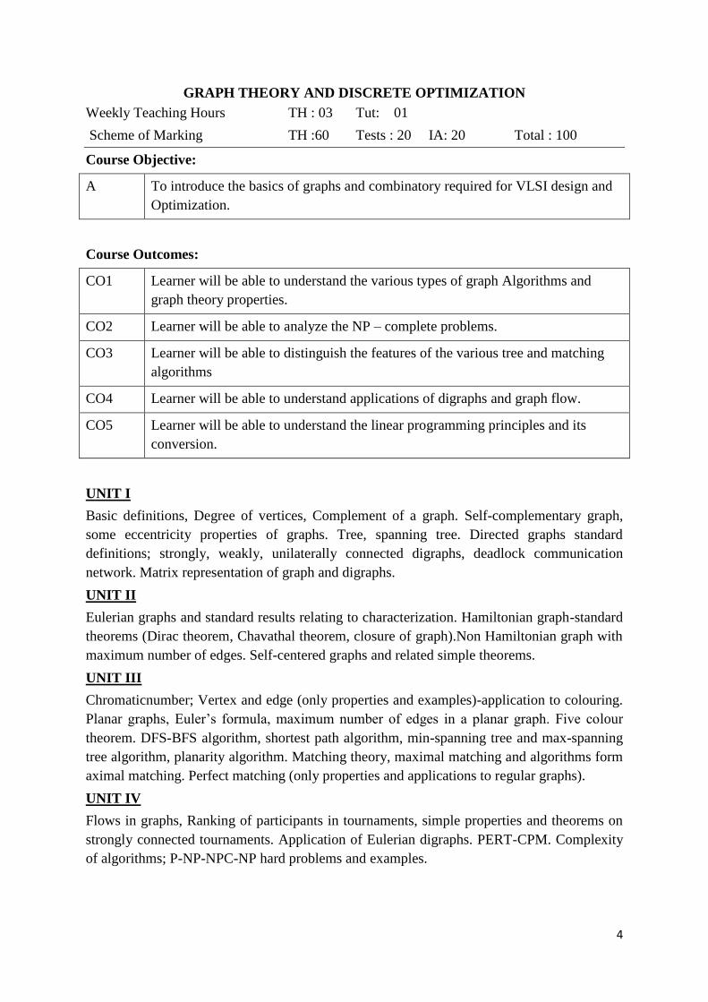
GRAPH THEORY AND DISCRETE OPTIMIZATION
Weekly Teaching Hours TH : 03 Tut: 01
Scheme of Marking TH :60 Tests : 20 IA: 20 Total : 100
Course Objective:
A To introduce the basics of graphs and combinatory required for VLSI design and
Optimization.
Course Outcomes:
CO1 Learner will be able to understand the various types of graph Algorithms and
graph theory properties.
CO2 Learner will be able to analyze the NP – complete problems.
CO3 Learner will be able to distinguish the features of the various tree and matching
algorithms
CO4 Learner will be able to understand applications of digraphs and graph flow.
CO5 Learner will be able to understand the linear programming principles and its
conversion.
UNIT I
Basic definitions, Degree of vertices, Complement of a graph. Self-complementary graph,
some eccentricity properties of graphs. Tree, spanning tree. Directed graphs standard
definitions; strongly, weakly, unilaterally connected digraphs, deadlock communication
network. Matrix representation of graph and digraphs.
UNIT II
Eulerian graphs and standard results relating to characterization. Hamiltonian graph-standard
theorems (Dirac theorem, Chavathal theorem, closure of graph).Non Hamiltonian graph with
maximum number of edges. Self-centered graphs and related simple theorems.
UNIT III
Chromaticnumber; Vertex and edge (only properties and examples)-application to colouring.
Planar graphs, Euler’s formula, maximum number of edges in a planar graph. Five colour
theorem. DFS-BFS algorithm, shortest path algorithm, min-spanning tree and max-spanning
tree algorithm, planarity algorithm. Matching theory, maximal matching and algorithms form
aximal matching. Perfect matching (only properties and applications to regular graphs).
UNIT IV
Flows in graphs, Ranking of participants in tournaments, simple properties and theorems on
strongly connected tournaments. Application of Eulerian digraphs. PERT-CPM. Complexity
of algorithms; P-NP-NPC-NP hard problems and examples.
5
UNIT V
Linear- Integer Linear programming, Conversion of TSP, maxflow, Knapsack scheduling,
shortest path problems for Linear programming types - branch bound method to solve
UNIT VI
Knapsack problems- critical path and linear programming conversion- Floor shop scheduling
problem- Personal assignment problem.
Dynamic programming- TSP- compartment problems- Best investment problems.
TEXTBOOKS /REFERENCE:
1. C. Papadimitriou & K. Steiglitz, Combinatorial Optimization, Prentice Hall, 1982.
2. H. Gerez, Algorithms for VLSI Design Automation, John Wiley, 1999.
3. B. Korte&J. Vygen, Combinatorial Optimization, Springer- Verlag, 2000.
4. Recent literature in Graph Theory and Discrete Optimization.
6
ANALOG IC DESIGN
Weekly Teaching Hours TH : 03 Tut: 01
Scheme of Marking TH :60 Tests : 20 IA: 20 Total : 100
Course Objective:
A
To develop the ability design and analyze MOS based Analog VLSI circuits to
draw the equivalent circuits of MOS based Analog VLSI and analyze their
performance.
B To develop the skills to design analog VLSI circuits for a given specification.
Course Outcomes:
CO1 Learner will be able to understand equivalent circuits of MOS based Analog VLSI
and analyze their performance.
CO2 Learner will be able to design analog VLSI circuits for a given specification.
CO3 Learner will be able to analyze the frequency response of the different
configurations of an amplifier.
CO4 Learner will be able to understand the feedback topologies involved in the
amplifier design.
CO5 Learner will be able to design features of the differential amplifiers.
UNIT I
Basic MOS Device Physics – General Considerations, MOS I/V Characteristics, Second
Order effects, MOS Device models. Short Channel Effects and Device Models. Single Stage
Amplifiers – Basic Concepts, Common Source Stage, Source Follower, Common Gate Stage,
Cascode Stage.
UNIT II
Differential Amplifiers – Single Ended and Differential Operation, Basic Differential Pair,
Common-Mode Response, Differential Pair with MOS loads, Gilbert Cell. Passive and
Active Current Mirrors – Basic Current Mirrors, Cascode Current Mirrors, Active Current
Mirrors.
UNIT III
Frequency Response of Amplifiers – General Considerations, Common Source Stage, Source
Followers, Common Gate Stage, Cascode Stage, Differential Pair. Noise – Types of Noise,
Representation of Noise in circuits, Noise in single stage amplifiers, Noise in Differential
Pairs.
UNIT IV
Feedback Amplifiers – General Considerations, Feedback Topologies, Effect of Loading.
7
UNIT V
Operational Amplifiers – General Considerations, One Stage Op Amps, Two Stage Op
Amps, Gain Boosting, Common – Mode Feedback, Input Range limitations, Slew Rate,
Power Supply Rejection, Noise in Op Amps. Stability and Frequency Compensation.
UNIT VI
Bandgap References, Introduction to Switched Capacitor Circuits, Nonlinearity and
Mismatch.
TEXTBOOKS / REFERENCE::
1. B.Razavi, Design of Analog CMOS Integrated Circuits, McGraw Hill Edition
2002.
2. Paul. R.Gray, Robert G. Meyer, Analysis and Design of Analog Integrated
Circuits, Wiley, (4/e), 2001.
3. D. A. Johns and K. Martin, Analog Integrated Circuit Design, Wiley, 1997.
4. R. Jacob Baker, CMOS Circuit Design, Layout, and Simulation, Wiley, (3/e), 2010.
5. P.E.Allen, D.R. Holberg, CMOS Analog Circuit Design, Oxford University Press, 2002.
6. Recent literature in Analog IC Design.
8
BASICS OF VLSI
Weekly Teaching Hours TH : 03 Tut: 01
Scheme of Marking TH :60 Tests : 20 IA: 20 Total : 100
Course Objective:
A To provide rigorous foundation in MOS and CMOS digital circuits.
B To train the students in transistor budgets, clock speeds and the growing
challenges of power consumption and productivity
Course Outcomes:
CO1 Learner will be able to implement the logic circuits using MOS and CMOS
technology.
CO2 Learner will be able to analyze various circuit configurations and their
applications.
CO3 Learner will be able to analyze the merits of circuits according to the technology
and applications change.
CO4 Learner will be able to design low power CMOS VLSI circuits.
CO5 Learner will be able to understand the rapid advances in CMOS Technology.
UNIT I
Introduction to CMOS circuits: MOS transistors, CMOS combinational logic gates,
multiplexers, latches and flip-flops, CMOS fabrication and layout, VLSI design flow.
UNIT II
MOS transistor theory: Ideal I-V and C-V characteristics, non-ideal I-V effects, DC transfer
characteristics, Switch level RC delay models.
UNIT III
CMOS technologies: Layout design rules, CMOS process enhancement, Technology related
CAD issues.
UNIT IV
Circuit characterization and performance estimation: Delay estimation, Logical effort and
Transistor sizing, Power dissipation, Interconnect design margin, Reliability, Scaling.
UNIT V
Circuit characterization and performance estimation: Power dissipation, Interconnect design
margin, Reliability, Scaling.
UNIT VI
Combinational circuit design: Static CMOS, Ratioed circuits, Cascode voltage switch logic,
Dynamic circuits, Pass transistor circuits.
9
TEXTBOOKS / REFERENCE::
1. N.H.E.Weste, D. Harris, CMOS VLSI Design (3/e), Pearson, 2005.
2. J.Rabey, M. Pedram, Digital Integrated circuits (2/e), PHI, 2003.
3. Pucknell & Eshraghian, Basic VLSI Design, (3/e), PHI, 1996.
4. Recent literature in Basics of VLSI.
10
ELECTIVE-I
DIGITAL SYSTEM DESIGN
Weekly Teaching Hours TH : 03 Tut: --
Scheme of Marking TH :60 Tests : 20 IA: 20 Total : 100
Course Objective:
A To get an idea about designing complex, high speed digital systems and how to
implement such design
Course Outcomes:
CO1 Learner will be able to identify mapping algorithms into architectures.
CO2 Learner will be able to understand various delays in combinational circuit and its
optimization methods.
CO3 Learner will be able to understand circuit design of latches and flip-flops
CO4 Learner will be able to demonstrate combinational and sequential circuits of
medium complexity that is based on VLSIs, and programmable logic devices.
CO5 Learner will be able to understand the advanced topics such as reconfigurable
computing, partially reconfigurable, Pipeline reconfigurable architectures and
block configurable.
UNIT I
Mapping algorithms into Architectures: Data path synthesis, control structures, critical path
and worst case timing analysis. FSM and Hazards.
UNIT II
Combinational network delay. Power and energy optimization in combinational logic circuit.
Sequential machine design styles. Rules for clocking. Performance analysis.
UNIT III
Sequencing static circuits. Circuit design of latches and flip-flops. Static sequencing element
methodology. Sequencing dynamic circuits. Synchronizers.
UNIT IV
Data path and array subsystems: Addition / Subtraction, Comparators, counters, coding,
multiplication and division.
UNIT V
SRAM, DRAM, ROM, serial access memory, context addressable memory.
UNIT VI
Reconfigurable Computing- Fine grain and Coarse grain architectures, Configuration
architectures-Single context, Multi context, partially reconfigurable, Pipeline reconfigurable,
11
Block Configurable, Parallel processing.
TEXTBOOKS / REFERENCE:
1. N. H.E.Weste, D. Harris, CMOS VLSI Design (3/e), Pearson, 2005.
2. W.Wolf, FPGA- based System Design, Pearson, 2004.
3. S.Hauck, A.DeHon, Reconfigurable computing: the theory and practice of FPGA-
basedcomputation, Elsevier, 2008.
4. F.P. Prosser, D. E. Winkel, Art of Digital Design, 1987.
5. R.F.Tinde, Engineering Digital Design, (2/e), Academic Press, 2000.
C. Bobda, Introduction to reconfigurable computing, Springer, 2007.
6. M.Gokhale, P.S.Graham, Reconfigurable computing: accelerating computation with
field-programmable gate arrays, Springer, 2005.
7. C.Roth, Fundamentals of Digital Logic Design, Jaico Publishers, V ed., 2009.
8. Recent literature in Digital System Design.
12
ELECTIVE-I
MODELING AND SYNTHESIS WITH VERILOG HDL
Weekly Teaching Hours TH : 03 Tut: --
Scheme of Marking TH :60 Tests : 20 IA: 20 Total : 100
Course Objective:
A To design combinational, sequential circuits using Verilog HDL.
B To understand behavioral and RTL modeling of digital circuits.
C To verify that a design meets its timing constraints, both manually and through
the use of computer aided design tools.
D To simulate, synthesize, and program their designs on a development board.
E To verify and design the digital circuit by means of Computer Aided Engineering
tools which involves in programming with the help of Verilog HDL.
Course Outcomes:
CO1 Learner will be able to understand the basic concepts of verilog HDL
CO2 Learner will be able to demonstrate digital systems in verilog HDL at different
levels of abstraction
CO3 Learner will be able to understand the simulation techniques and test bench
creation.
CO4 Learner will be able to understand the design flow from simulation to
synthesizable version
CO5 Learner will be able to understand the process of synthesis and post-synthesis
UNIT I
Hardware modeling with the verilog HDL.Encapsulation, modeling primitives, different
types of description.
UNIT II
Logic system, data types and operators for modeling inverilog HDL.
UNIT III
Verilog Models of propagation delay and net delay path delays and simulation, inertial delay
effects and pulse rejection.
UNIT IV
Behavioral descriptions in verilogHDL.Synthesis of combinational logic.
13
UNIT V
HDL-based synthesis - technology-independent design, styles for synthesis of combinational
and sequential logic, synthesis of finite state machines, synthesis of gated clocks, design
partitions and hierarchical structures.
UNIT VI
Synthesis of language constructs, nets, register variables, expressions and operators,
assignments and compiler directives. Switch-level models in verilog. Design examples in
verilog.
TEXTBOOKS / REFERENCE:
1. M.D.Ciletti, Modeling, Synthesis and Rapid Prototyping with the Verilog HDL,
PHI, 1999.
2. S. Palnitkar, Verilog HDL – A Guide to Digital Design and Synthesis, Pearson,
2003.
3. J Bhaskar, A Verilog HDL Primer (3/e), Kluwer, 2005.
4. M.G.Arnold, Verilog Digital – Computer Design, Prentice Hall (PTR), 1999.
5. Recent literature in Modeling and Synthesis with Verilog HDL.
14
ELECTIVE-I
OPTIMIZATIONS OF DIGITAL SIGNAL PROCESSING STRUCTURES FOR VLSI
Weekly Teaching Hours TH : 03 Tut: --
Scheme of Marking TH :60 Tests : 20 IA: 20 Total : 100
Course Objective:
A To understand the various VLSI architectures for digital signal processing.
B To know the techniques of critical path and algorithmic strength reduction in the
filter structures.
C To enable students to design VLSI system with high speed and low power.
D To encourage students to develop a working knowledge of the central ideas of
implementation of DSP algorithm with optimized hardware.
Course Outcomes:
CO1 Learner will be able to understand the overview of DSP concepts and design
architectures for DSP algorithms.
CO2 Learner will be able to improve the overall performance of DSP system through
various transformation and optimization techniques.
CO3 Learner will be able to perform pipelining and parallel processing on FIR and IIR
systems to achieve highspeed and low power.
CO4 Learner will be able to optimize design in terms of computation complexity and
speed.
CO5 Learner will be able to understand clock based issues and design asynchronous and
wave pipelined systems.
UNIT I
An overview of DSP concepts, Pipelining of FIR filters. Parallel processing of FIR filters.
Pipelining and parallel processing for low power, Combining Pipelining and Parallel
Processing.
UNIT II
Transformation Techniques: Iteration bound, Retiming, Folding and Unfolding
UNIT III
Pipeline interleaving in digital filters. Pipelining and parallel processing for IIR filters. Low
power IIR filter design using pipelining and parallel processing, Pipelined adaptive digital
filters.
15
UNIT IV
Algorithms for fast convolution: Cook-Toom Algorithm, Cyclic Convolution. Algorithmic
strength reduction in filters and transforms: Parallel FIR Filters, DCT and inverse DCT,
Parallel Architectures for Rank-Order Filters.
UNIT V
Synchronous pipelining and clocking styles, clock skew and clock distribution in bit level
pipelined VLSI designs.
UNIT VI
Wave pipelining, constraint space diagram and degree of wavepipelining, Implementation of
wave-pipelined systems, Asynchronous pipelining.
TEXTBOOKS / REFERENCE:
1. K.K.Parhi, VLSI Digital Signal Processing Systems, John-Wiley, 2007
2. U. Meyer -Baese, Digital Signal Processing with FPGAs, Springer, 2004
3. Wayne Burleson, KonstantinosKonstantinides, Teresa H. Meng, VLSI Signal
Processing, 1996.
4. Richard J. Higgins, Digital signal processing in VLSI, 1990.
5. Sun Yuan Kung, Harper J. Whitehouse, VLSI and modern signal processing, 1985
6. Magdy A. Bayoumi, VLSI Design Methodologies for Digital Signal Processing, 2012
7. Earl E. Swartzlander, VLSI signal processing systems, 1986. Recent literature in
Optimizations of Digital Signal Processing Structures for VLSI.
16
ELECTIVE-I
COGNITIVE RADIO
Weekly Teaching Hours TH : 03 Tut: --
Scheme of Marking TH :60 Tests : 20 IA: 20 Total : 100
Course Objectives:
A To understand the use of the SDR
B To understand the stages of the evolution of SDR.
C To study the applications of the Cognitive Radio.
D To develop the system model for the spectrum sensing and spectrum access
techniques in CR.
Course Outcomes:
CO1 Learner will be able to differentiate between SDR and CR
CO2 Learner will be able to evaluate the different spectrum sensing techniques for the
cognitive radio.
CO3 Learner will be able to develop the system model for single carrier and multicarrier
cognitive radio system.
CO4 Learner will be able to evaluate the different spectrum management techniques for
cognitive radio system.
C05 Learner will be able to simulate and analyze the SDR and Cognitive radio systems
UNIT I
Software Defined Radio Architecture - Digital Signal Processor and SDR Baseband
Architecture, Reconfigurable Wireless Communication Systems, Unified Communication
Algorithm , Reconfigurable OFDM Implementation, Reconfigurable OFDM and CDMA,
Digital Radio Processing , Conventional RF, Digital Radio Processing (DRP) Based System
Architecture
UNIT II
Cooperative Communications and Networks - Information Theory for Cooperative
Communications, Fundamental Network Information, Multiple-access Channel with
Cooperative Diversity, Cooperative Communications, Three-Node Cooperative
Communications ,Multiple-Node Relay Network,Cooperative Wireless Networks, Benefits of
Cooperation in Wireless Networks , Cooperation in Cluster-Based Ad-hoc Networks
UNIT III
Cognitive Radio Communications : Cognitive Radios and Dynamic Spectrum Access,The
Capability of Cognitive Radios, Cognitive Radio cycle, Spectrum Sharing Models of DSA,
17
Opportunistic Spectrum Access: Basic Components , Networking The Cognitive Radios,
Analytical Approach and Algorithms for Dynamic Spectrum Access, Dynamic Spectrum
Access in Open Spectrum ,Opportunistic Spectrum Access , Opportunistic Power Control
,Fundamental Limits of Cognitive Radios, Mathematical Models Toward Networking
Cognitive Radios, CR Link Model, Overlay CR Systems, Rate-Distance Nature .
UNIT IV
Spectrum Sensing: Primary Signal Detection such as Energy Detector, Cyclo-stationary
Feature Detector ,Matched Filter, Cooperative Sensing etc., Spectrum Sensing to Detect
Specific Primary System , conventional Spectrum Sensing, Power Control , Power-Scaling
Power Control ,Cooperative Spectrum Sensing , Spectrum Sensing for Cognitive OFDMA
Systems , Discrimination of States of the Primary System, Spectrum Sensing Procedure,
Spectrum Sensing for Cognitive Multi-Radio Networks , Multiple System Sensing , Radio
Resource Sensing.
UNIT V
Cognitive Radio Networks: Network Coding for Cognitive Radio Relay Networks , System
Model, Network Capacity Analysis on Fundamental CRRN Topologies, Link Allocation ,
Numerical Results, Cognitive Radio Networks Architecture , Network Architecture ,Links in
CRN , IP Mobility Management in CRN ,Terminal Architecture of CRN, Cognitive Radio
Device Architecture , Re-configurable MAC ,Radio Access Network Selection ,QoS
Provisional Diversity Radio Access Networks , Cooperative/Collaborative Diversity and
Efficient Protocols , Statistical QoS Guarantees over Wireless Asymmetry Collaborative
Relay Networks.
UNIT VI
Spectrum access and sharing: Unlicensed Spectrum Sharing, Licensed Spectrum Sharing ,
Secondary(SSA) Spectrum Access ,Non-Real-Time SSA, Real-Time SSA, Negotiated
Access , Is Quality of Service Provisioning Possible in a Shared Band, Opportunistic Access
,Overlay Approach , Underlay Approach
Text /Reference Books:
1. Kwang-Cheng Chen, Ramjee Prasad, Cognitive Radio Networks, John Wiley & Sons
Ltd.
2. Alexander M. Wyglinski, Maziar Nekovee, Y. Thomas Hou, Cognitive Radio
Communications and Networks Principles and Practice, Elsevier publication.
3. Qusay H. Mahmoud, Cognitive Networks, John Wiley & Sons Ltd.
18
ELECTIVE-I
VLSI PROCESS TECHNOLOGY
Weekly Teaching Hours TH : 03 Tut: --
Scheme of Marking TH :60 Tests : 20 IA: 20 Total : 100
Course Objective:
A To provide rigorous foundation in MOS and CMOS fabrication process.
Course Outcomes:
CO1 Learner will be able to understand various techniques involved in the VLSI
fabrication process.
CO2 Learner will be able to understand the different lithography methods and etching
process
CO3 Learner will be able to analyze the deposition and diffusion mechanisms.
CO4 Learner will be able to analyze the fabrication of NMOS, CMOS memory and
bipolar devices
CO5 Learner will be able to understand the nuances of assembly and packaging of VLSI
devices.
UNIT I
Electron grade silicon. Crystal growth. Wafer preparation. Vapor phase and molecular beam
epitaxy. SOI. Epitaxial evaluation. Oxidation techniques, systems and properties. Oxidation
defects.
UNIT II
Optical, electron, X-ray and ion lithography methods. Plasma properties, size, control, etch
mechanism, etch techniques and equipments.
UNIT III
Deposition process and methods. Diffusion in solids. Diffusion equation and diffusion
mechanisms.
UNIT IV
Ion implantation and metallization. Process simulation of ion implementation, diffusion,
oxidation, epitaxy, lithography, etching and deposition.
UNIT V
NMOS, CMOS, MOS memory and bipolar IC technologies. IC fabrication.
UNIT VI
Analytical and assembly techniques. Packaging of VLSI devices.
19
TEXTBOOKS / REFERENCE:
1. S.M.Sze, “VLSI Technology (2/e)” , McGraw Hill, 1988
2. W. Wolf, “Modern VLSI Design”, (3/e), Pearson,2002
20
ELECTIVE-II
ADVANCED COMPUTER ARCHITECTURE
Weekly Teaching Hours TH : 03 Tut: --
Scheme of Marking TH :60 Tests : 20 IA: 20 Total : 100
Course Objective:
A To give an exposure on look ahead pipelining- parallelism, multiprocessor
scheduling, multithreading and various memory organizations.
Course Outcomes:
CO1 Learner will be able to apply the basic knowledge of partitioning and scheduling in
Multiprocessors.
CO2 Learner will be able to analyze and design cache memory, virtual memory and
shared memory organizations.
CO3 Learner will be able to distinguish and analyze the design properties of Linear and
Non – Linear processors.
CO4 Learner will be able to analyze the principles of multithreading in hybrid
Architectures.
CO5 Learner will be able to analyze any parallel programming models for various
architectures and
Applications.
UNIT I
Multiprocessors and multi-computers. Multi-vector and SIMD computers. PRAM and VLSI
Models. Conditions of parallelism. Program partitioning and scheduling. Program flow
mechanisms. Parallel processing applications. Speed up performance law.
UNIT II
Advanced processor technology. Superscalar and vector processors. Memory hierarchy
technology. Virtual memory technology. Cache memory organization. Shared memory
organization.
UNIT III
Linear pipeline processors. Non-linear pipeline processors. Instruction pipeline design.
Arithmetic design. Superscalar and super pipeline design. Multiprocessor system
interconnects. Message passing mechanisms.
UNIT IV
Vector Processing principle. Multivector multiprocessors, Compound Vector processing.
Principles of multithreading, Fine grain multicomputer. Scalable and multithread
architectures. Dataflow and hybrid architectures.
21
UNIT V
Parallel programming models. Parallel languages and compilers. Parallel programming
environments. Synchronization and multiprocessing modes.
UNIT VI
Message passing program development. Mapping programs onto multicomputer.
Multiprocessor UNIX design goals. MACH/OS kernel architecture. OSF/1 architecture and
applications.
TEXTBOOKS / REFERENCE:
1 M.J. Quinn, “Designing Efficient Algorithms for Parallel Computer’, McGraw Hill,
2 K. Hwang, “Advanced Computer Architecture “, Tata McGraw Hill, 2001.
3 W. Stallings,” Computer Organization and Architecture”, McMillan, 1990
4 Recent literature in Advanced Computer Architecture.
22
ELECTIVE-II
LOW POWER VLSI CIRCUITS
Weekly Teaching Hours TH : 03 Tut: --
Scheme of Marking TH :60 Tests : 20 IA: 20 Total : 100
Course Objective:
A To expose the students to the low voltage device modeling, low voltage, low power
VLSI CMOS circuit design.
Course Outcomes:
CO1 Learner will be able to acquire the knowledge about various CMOS fabrication
process and its modeling.
CO2 Learner will be able to infer about the second order effects of MOS transistor
characteristics.
CO3 Learner will be able to analyze and implement various CMOS static logic circuits.
CO4 Learner will be able to understand the design of various CMOS dynamic logic
circuits.
CO5 Learner will be able to understand the design techniques low voltage and low power
CMOS circuits for various applications.
CO6 Learner will be able to understand the different types of memory circuits and their
design.
CO7 Learner will be able to design and implement various structures for low power
applications.
UNIT I
Evolution of CMOS technology.0.25 µm and 0.1 µm technologies. Shallow trench isolation.
Lightly-doped drain. Buried channel. BiCMOS and SOI CMOS technologies. Second order
effects and capacitance of MOS devices.
UNIT II
CMOS inverters, static logic circuits of CMOS, pass transistor, BiCMOS, SOI CMOS and
low power CMOS techniques
UNIT III
Basic concepts of dynamic logic circuits. Various problems associated with dynamic logic
circuits.
UNIT IV
Differential, BiCMOS and low voltage dynamic logic circuits.
UNIT V
Different types of memory circuits
23
UNIT VI
Adder circuits, Multipliers and advanced structures – PLA, PLL, DLL and processing unit.
TEXTBOOKS / REFERENCE:
1 J.Rabaey, “Low Power Design Essentials (Integrated Circuits and Systems)”,
Springer, 2009
2 J.B.Kuo&J.H.Lou, “Low-voltage CMOS VLSI Circuits”, Wiley, 1999.
3 A.Bellaowar& M.I.Elmasry,”Low power Digital VLSI Design, Circuits and Systems”,
Kluwer, 1996.
4 Recent literature in Low Power VLSI Circuits.
24
ELECTIVE-II
VLSI DIGITAL SIGNAL PROCESSING SYSTEMS
Weekly Teaching Hours TH : 03 Tut: --
Scheme of Marking TH :60 Tests : 20 IA: 20 Total : 100
Course Objective::
A To enable students to design VLSI systems with high speed and low power.
B To encourage students to develop a working knowledge of the central ideas of
implementation of DSP algorithm with optimized hardware.
Course Outcomes:
CO1 Learner will be able to acquire the knowledge of round off noise computation and
numerical strength reduction.
CO2 Learner will be able to design Bit level and redundant arithmetic Architectures.
UNIT I
An overview of DSP concepts, Representations of DSP algorithms. Systolic Architecture
Design: FIR Systolic Array, Matrix-Matrix Multiplication, 2D Systolic Array Design. Digital
Lattice Filter Structures: Schur Algorithm, Derivation of One-Multiplier Lattice Filter,
Normalized Lattice Filter, Pipelining of Lattice Filter.
UNIT II
Scaling and Round off Noise - State variable description of digital filters, Scaling and Round
off Noise computation, Round off Noise in Pipelined IIR Filters, Round off Noise
Computation using state variable description, Slow-down, Retiming and Pipelining.
UNIT III
Bit level arithmetic Architectures- parallel multipliers, interleaved floor-plan and bit-plane
based digital filters, Bit serial multipliers, Bit serial filter design and implementation,
Canonic signed digit arithmetic, Distributed arithmetic.
UNIT IV
Redundant arithmetic -Redundant number representations, carry free radix-2 addition and
subtraction, Hybrid radix-4 addition, Radix-2 hybrid redundant multiplication architectures,
data format conversion, Redundant to Non-redundant converter.
UNIT V
Numerical Strength Reduction - Sub expression Elimination, Multiple Constant
Multiplication,
UNIT VI
Sub expression sharing in Digital Filters, Additive and Multiplicative Number Splitting.
25
TEXTBOOKS / REFERENCE:
1 K.K.Parhi, “VLSI Digital Signal Processing Systems”, John-Wiley, 2007.
2 JU. Meyer -Baese, Digital Signal Processing with FPGAs, Springer, 2004.
3 Recent literature in VLSI Digital Signal Processing Systems.
26
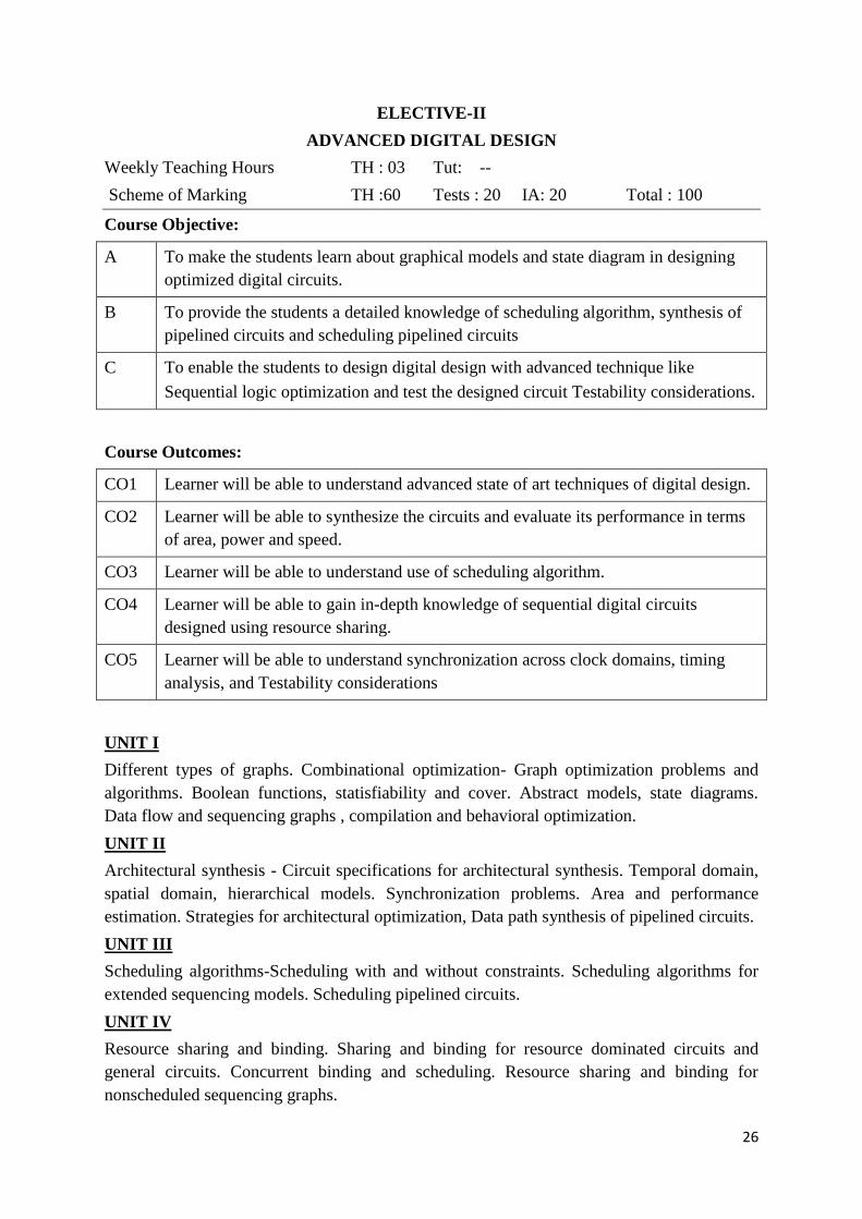
ELECTIVE-II
ADVANCED DIGITAL DESIGN
Weekly Teaching Hours TH : 03 Tut: --
Scheme of Marking TH :60 Tests : 20 IA: 20 Total : 100
Course Objective:
A To make the students learn about graphical models and state diagram in designing
optimized digital circuits.
B To provide the students a detailed knowledge of scheduling algorithm, synthesis of
pipelined circuits and scheduling pipelined circuits
C To enable the students to design digital design with advanced technique like
Sequential logic optimization and test the designed circuit Testability considerations.
Course Outcomes:
CO1 Learner will be able to understand advanced state of art techniques of digital design.
CO2 Learner will be able to synthesize the circuits and evaluate its performance in terms
of area, power and speed.
CO3 Learner will be able to understand use of scheduling algorithm.
CO4 Learner will be able to gain in-depth knowledge of sequential digital circuits
designed using resource sharing.
CO5 Learner will be able to understand synchronization across clock domains, timing
analysis, and Testability considerations
UNIT I
Different types of graphs. Combinational optimization- Graph optimization problems and
algorithms. Boolean functions, statisfiability and cover. Abstract models, state diagrams.
Data flow and sequencing graphs , compilation and behavioral optimization.
UNIT II
Architectural synthesis - Circuit specifications for architectural synthesis. Temporal domain,
spatial domain, hierarchical models. Synchronization problems. Area and performance
estimation. Strategies for architectural optimization, Data path synthesis of pipelined circuits.
UNIT III
Scheduling algorithms-Scheduling with and without constraints. Scheduling algorithms for
extended sequencing models. Scheduling pipelined circuits.
UNIT IV
Resource sharing and binding. Sharing and binding for resource dominated circuits and
general circuits. Concurrent binding and scheduling. Resource sharing and binding for
nonscheduled sequencing graphs.
27
UNIT V
Sequential logic optimization-sequential circuit optimization using state based models and
network models
UNIT VI
Implicit finite state machine. Traversal methods. Testability considerations for synchronous
circuits.
TEXTBOOKS / REFERENCE:
1 G.DeMicheli, “Synthesis and optimization of Digital circuits”, McGraw Hill,1994 .
2 C. Roth, “Fundamentals of Digital Logic Design”, Jaico Publishers, V ed., 2009.
3 Balabanian, “Digital Logic Design Principles”, Wiley publication, 2000.
4 J. F. Wakerly,”Digital Design principles and practices”, 3rd edition, PHI publication, .
5. S.Brown, “Fundamentals of digital logic”, Tata McGraw Hill publication, 2007.
6 . N. N. Biswas, “Logic Design Theory”, Prentice Hall of India, 2001
7 . John M Yarbrough, “Digital Logic applications and Design”, Thomson Learning.
8. Recent literature in Advanced Digital Design.
28
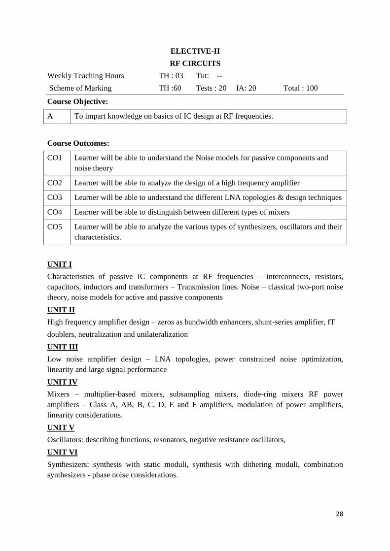
ELECTIVE-II
RF CIRCUITS
Weekly Teaching Hours TH : 03 Tut: --
Scheme of Marking TH :60 Tests : 20 IA: 20 Total : 100
Course Objective:
A To impart knowledge on basics of IC design at RF frequencies.
Course Outcomes:
CO1 Learner will be able to understand the Noise models for passive components and
noise theory
CO2 Learner will be able to analyze the design of a high frequency amplifier
CO3 Learner will be able to understand the different LNA topologies & design techniques
CO4 Learner will be able to distinguish between different types of mixers
CO5 Learner will be able to analyze the various types of synthesizers, oscillators and their
characteristics.
UNIT I
Characteristics of passive IC components at RF frequencies – interconnects, resistors,
capacitors, inductors and transformers – Transmission lines. Noise – classical two-port noise
theory, noise models for active and passive components
UNIT II
High frequency amplifier design – zeros as bandwidth enhancers, shunt-series amplifier, fT
doublers, neutralization and unilateralization
UNIT III
Low noise amplifier design – LNA topologies, power constrained noise optimization,
linearity and large signal performance
UNIT IV
Mixers – multiplier-based mixers, subsampling mixers, diode-ring mixers RF power
amplifiers – Class A, AB, B, C, D, E and F amplifiers, modulation of power amplifiers,
linearity considerations.
UNIT V
Oscillators: describing functions, resonators, negative resistance oscillators,
UNIT VI
Synthesizers: synthesis with static moduli, synthesis with dithering moduli, combination
synthesizers - phase noise considerations.
29
TEXTBOOKS / REFERENCE:
1. T.homas H. Lee, “The Design of CMOS Radio-Frequency Integrated Circuits”, 2nd ed.,
Cambridge, UK: Cambridge University Press, 2004.
2. B.Razavi, “RF Microelectronics”, 2nd Ed., Prentice Hall, 1998.
3. Abidi, P.R. Gray, and R.G. Meyer, eds. , “Integrated Circuits for Wireless
Communications”, New York: IEEE Press, 1999.
4. R. Ludwig and P. Bretchko, “RF Circuit Design, Theory and Applications”, Pearson,
2000.
5. Mattuck,A., “Introduction to Analysis”, Prentice-Hall,1998.
6. Recent literature in RF Circuits.
30
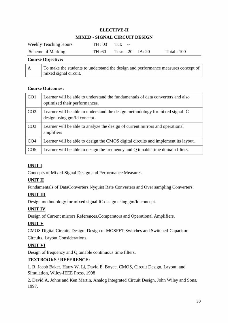
ELECTIVE-II
MIXED - SIGNAL CIRCUIT DESIGN
Weekly Teaching Hours TH : 03 Tut: --
Scheme of Marking TH :60 Tests : 20 IA: 20 Total : 100
Course Objective:
A To make the students to understand the design and performance measures concept of
mixed signal circuit.
Course Outcomes:
CO1 Learner will be able to understand the fundamentals of data converters and also
optimized their performances.
CO2 Learner will be able to understand the design methodology for mixed signal IC
design using gm/Id concept.
CO3 Learner will be able to analyze the design of current mirrors and operational
amplifiers
CO4 Learner will be able to design the CMOS digital circuits and implement its layout.
CO5 Learner will be able to design the frequency and Q tunable time domain filters.
UNIT I
Concepts of Mixed-Signal Design and Performance Measures.
UNIT II
Fundamentals of DataConverters.Nyquist Rate Converters and Over sampling Converters.
UNIT III
Design methodology for mixed signal IC design using gm/Id concept.
UNIT IV
Design of Current mirrors.References.Comparators and Operational Amplifiers.
UNIT V
CMOS Digital Circuits Design: Design of MOSFET Switches and Switched-Capacitor
Circuits, Layout Considerations.
UNIT VI
Design of frequency and Q tunable continuous time filters.
TEXTBOOKS / REFERENCE:
1. R. Jacob Baker, Harry W. Li, David E. Boyce, CMOS, Circuit Design, Layout, and
Simulation, Wiley-IEEE Press, 1998
2. David A. Johns and Ken Martin, Analog Integrated Circuit Design, John Wiley and Sons,
1997.
31
COMMUNICATION SKILLS
Weekly Teaching Hours TH: 02 Practical: -
Scheme of Marking TH: -- IA: 25 PR/OR: 25 Total: 50
Course Objectives:
A To become more effective confident speakers and deliver persuasive presentations
B To develop greater awareness and sensitivity to some important considerations in
interpersonal communication and learn techniques to ensure smoother interpersonal
relations
Course Outcomes:
CO1 Learner will be able to understand the fundamental principles of effective business
communication
CO2 Learner will be able to apply the critical and creative thinking abilities necessary for
effective communication in today's business world
CO3 Learner will be able to organize and express ideas in writing and speaking to produce
messages suitably tailored for the topic, objective, audience, communication medium
and context
CO4 Learner will be able to demonstrate clarity, precision, conciseness and coherence in
your use of language
CO5 Learner will be able to become more effective confident speakers and deliver
persuasive presentations
UNIT I
Introduction to communication, Necessity of communication skills, Features of good
communication, Speaking skills, Feedback & questioning technique, Objectivity in argument
UNIT II
Verbal and Non-verbal Communication, Use and importance of non-verbal communication
while using a language, Study of different pictorial expressions of non-verbal communication
and their analysis
UNIT III
Academic writing, Different types of academic writing, Writing Assignments and Research
Papers, Writing dissertations and project reports
UNIT IV
Presentation Skills: Designing an effective Presentation, Contents, appearance, themes in a
presentation; Tone and Language in a presentation, Role and Importance of different tools for
effective presentation
UNIT V
Motivation/ Inspiration: Ability to shape and direct working methods according to self-
defined criteria;Ability to think for oneself, Apply oneself to a task independently with self-
motivation, Motivation techniques: Motivation techniques based on needs and field situations
32
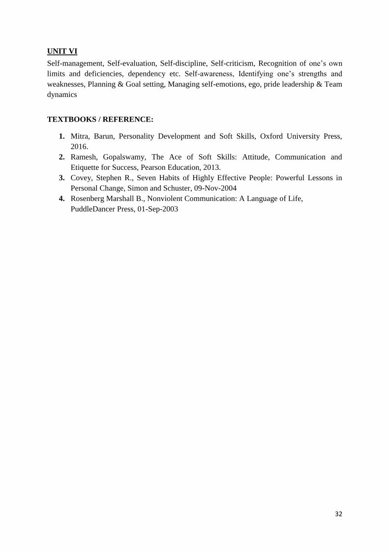
UNIT VI
Self-management, Self-evaluation, Self-discipline, Self-criticism, Recognition of one’s own
limits and deficiencies, dependency etc. Self-awareness, Identifying one’s strengths and
weaknesses, Planning & Goal setting, Managing self-emotions, ego, pride leadership & Team
dynamics
TEXTBOOKS / REFERENCE:
1. Mitra, Barun, Personality Development and Soft Skills, Oxford University Press,
2016.
2. Ramesh, Gopalswamy, The Ace of Soft Skills: Attitude, Communication and
Etiquette for Success, Pearson Education, 2013.
3. Covey, Stephen R., Seven Habits of Highly Effective People: Powerful Lessons in
Personal Change, Simon and Schuster, 09-Nov-2004
4. Rosenberg Marshall B., Nonviolent Communication: A Language of Life,
PuddleDancer Press, 01-Sep-2003
33
PG LAB-I
Weekly Teaching Hours TH: -- Practical: 03
Scheme of Marking TH: -- IA: 25 PR/OR: 25 Total: 50
Practical’s of the Lab - I shall be based on the courses of first semester. The lab work shall
consist of hands on experiments on the different software and hardware platforms related to
the syllabus.
34
VLSI SYSTEM TESTING
Weekly Teaching Hours TH : 03 Tut: 01
Scheme of Marking TH :60 Tests : 20 IA: 20 Total : 100
Course Objective:
A To expose the students, the basics of testing techniques for VLSI circuits and Test
Economics.
Course Outcomes:
CO1 Learner will be able to apply the concepts in testing which can help them design a
better yield in IC design.
CO2 Learner will be able to tackle the problems associated with testing of
semiconductor circuits at earlier design levels so as to significantly reduce the
testing costs.
CO3 Learner will be able to analyze the various test generation methods for static &
dynamic CMOS circuits.
CO4 Learner will be able to identify the design for testability methods for
combinational & sequential CMOS circuits.
CO5 Learner will be able to recognize the BIST techniques for improving testability.
UNIT I
Basics of Testing: Fault models, Combinational logic and fault simulation, Test generation
for Combinational Circuits. Current sensing based testing. Classification of sequential ATPG
methods. Fault collapsing and simulation
UNIT II
Universal test sets: Pseudo-exhaustive and iterative logic array testing. Clocking schemes for
delay fault testing. Testability classifications for path delay faults. Test generation and fault
simulation for path and gate delay faults.
UNIT III
CMOS testing: Testing of static and dynamic circuits. Fault diagnosis: Fault models for
diagnosis, Cause-effect diagnosis, Effect-cause diagnosis.
UNIT IV
Design for testability: Scan design, Partial scan, use of scan chains, boundary scan, DFT for
other test objectives, Memory Testing.
UNIT V
Built-in self-test: Pattern Generators, Estimation of test length, Test points to improve
Testability.
35
UNIT VI
Analysis of aliasing in linear compression, BIST methodologies, BIST for delay fault testing.
TEXTBOOKS / REFERENCE:
1. N. Jha& S.D. Gupta, “Testing of Digital Systems”, Cambridge, 2003.
2. W. W. Wen, “VLSI Test Principles and Architectures Design for Testability”, Morgan
Kaufmann Publishers. 2006
3. Michael L. Bushnell &Vishwani D. Agrawal,” Essentials of Electronic Testing for
Digital, memory & Mixed signal VLSI Circuits”, Kluwar Academic Publishers. 2000.
4. P. K. Lala,” Digital circuit Testing and Testability”, Academic Press. 1997.
5. M. Abramovici, M. A. Breuer, and A.D. Friedman, “Digital System Testing and Testable
Design”, Computer Science Press, 1990.
6. Recent literature in VLSI System Testing.
36
DESIGN OF ASICS
Weekly Teaching Hours TH : 03 Tut: 01
Scheme of Marking TH :60 Tests : 20 IA: 20 Total : 100
Course Objective:
A To prepare the student to be an entry-level industrial standard ASIC or FPGA
designer.
B To give the student an understanding of issues and tools related to ASIC/FPGA
design and implementation.
C To give the student an understanding of basics of System on Chip and Platform
based design.
D To give the student an understanding of High performance algorithms
Course Outcomes:
CO1 Learner will be able to demonstrate VLSI tool-flow and appreciate FPGA and
CPLD architectures
CO2 Learner will be able to understand the issues involved in ASIC design, including
technology choice, design management and tool-flow.
CO3 Learner will be able to understand the algorithms used for ASIC construction
CO4 Learner will be able to understand Full Custom Design Flow and Tool used
CO5 Learner will be able to understand Semicustom Design Flow and Tool used - from
RTL to GDS and Logical to Physical Implementation
CO6 Learner will be able to understand about STA, LEC, DRC, LVS, DFM
CO7 Learner will be able to understand the basics of System on Chip and on chip
communication architectures appreciate high performance algorithms for ASICs
UNIT I
Introduction to Technology, Types of ASICs, VLSI Design flow, Design and Layout Rules,
Programmable ASICs - Antifuse, SRAM, EPROM, EEPROM based ASICs. Programmable
ASIC logic cells and I/O cells. Programmable interconnects. Advanced FPGAs and CPLDs
and Soft-core processors.
UNIT II
ASIC physical design issues, System Partitioning, Floorplanning and Placement. Algorithms:
K-L, FM, Simulated annealing algorithms. Full Custom Design: Basics, Needs &
Applications. Schematic and layout basics, Full Custom Design Flow.
37
UNIT III
Semicustom Approach: Synthesis (RTL to GATE netlist) - Introduction to Constraints
(SDC), Introduction to Static Timing Analysis (STA). Place and Route (Logical to Physical
Implementation): Floorplan and Power-Plan, Placement, Clock Tree Synthesis (clock
planning), Routing, Timing Optimization, GDS generation.
UNIT IV
Extraction, Logical equivalence and STA: Parasitic Extraction Flow, STA: Timing Flow,
LEC: Introduction, flow and Tools used. Physical Verification: Introduction, DRC, LVS and
basics of DFM.
UNIT V
System-On-Chip Design - SoC Design Flow, Platform-based and IP based SoC Designs,
Basic Concepts of Bus-Based Communication Architectures.
UNIT VI
High performance algorithms for ASICs/ SoCs as case studies – Canonic Signed Digit
Arithmetic, KCM, Distributed Arithmetic, High performance digital filters for sigma-delta
ADC.
TEXTBOOKS / REFERENCE:
1. N. Jha & S.D. Gupta, “Testing of Digital Systems”, Cambridge, 2003.
2. M.J.S. Smith : Application Specific Integrated Circuits, Pearson, 2003
3. Sudeep Pasricha and Nikil Dutt, On-Chip Communication Architectures System on
Chip Interconnect, Elsevier, 2008
4. H. Gerez, Algorithms for VLSI Design Automation, John Wiley, 1999
5. Jan. M.Rabaey et al, Digital Integrated Circuit Design Perspective (2/e), PHI 2003
7. David A.Hodges, Analysis and Design ofDigital Integrated Circuits (3/e), MGH 2004
8. Hoi-Jun Yoo, KangminLeeand Jun Kyong Kim, Low-Power NoC for
HighPerformanceSoC Design, CRC Press, 2008
9. An Integrated Formal Verification solution DSM sign-off market
trends,www.cadence.com.
38
ELECTIVE-III
FUNCTIONAL VERIFICATION USING HARDWARE VERIFICATION
LANGUAGES
Weekly Teaching Hours TH : 03 Tut: --
Scheme of Marking TH :60 Tests : 20 IA: 20 Total : 100
Course Objective:
A Learn to use verification tools and experiment on actual circuits designed in industry
Course Outcomes:
CO1 Learner will be able to understand fundamentals of data converters and also
optimized their performances.
CO2 Learner will be able to understand the design methodology for mixed signal IC
design using gm/Id concept
CO3 Learner will be able to analyze the design of current mirrors and operational
amplifiers
CO4 Learner will be able to design the CMOS digital circuits and implement its layout.
CO5 Learner will be able to design the frequency and Q tunable time domain filters.
UNIT I
System Verilog (SV) - Data Types, Arrays, Structures, Unions, Procedural Blocks, Tasks &
Functions, Procedural Statements, Interfaces, Basic OOPs, Randomization, Threads & Inter
Process Communication, Advanced OOPs & Test bench guidelines, Advanced Interfaces
UNIT II
A Complete System Verilog Test Bench (SVTB), Functional Coverage in System Verilog,
Interfacing with C, FSM Modeling with SV, Connecting Test bench & Design, Behavioral &
Transaction Level Modeling with SV.
UNIT III
System Verilog Assertions (SVA) – Introduction to SVA, Building blocks, Properties,
Boolean expressions, Sequence, Single & Multiple Clock definitions, Implication operators
(Overlapping & Non-overlapping), Repeatition operators, Built-in System functions ($past,
$stable, $onehot, $onehot0, $isunknown), Constructs (ended, and, intersect, or, first_match,t
throughout, within, disableiff, expect, matched, if –else), assertion directives, nested
implication, formal arguments in property
UNIT IV
SVA using local variables, calling subroutines, SVA for functional coverage, Connecting
SVA to the Design or Test bench, SVA for FSMs, Memories, Protocol checkers, SVA
Simulation Methodology
UNIT V
39
Assertions: Practice & Methodology, Re-use of Assertions, Tracking coverage with
Assertions, Using SVA with other languages.
UNIT VI
Functional Verification coverage using design, verification languages and implementation
standards: Verilog IEEE 1364, VHDL IEEE 1076, System Verilog IEEE 1800, Property
Specific Language (PSL) IEEE 1850, System C™ IEEE 1666, Encryption IEEE 1735, e
Verification Language IEEE 1647, Open Verification Methodology (OVM) and Universal
Verification Methodology (UVM).
TEXTBOOKS / REFERENCE:
1. Stuart Sutherland, Simon Davidmann, System Verilog for design: a guide to using System
Verilog for hardware design and modeling published by Springer, 2004 ISBN 1402075308,
9781402075308
2. System Verilog for Verification: A Guide to Learning the Test bench Language Features
by Chris Spear Edition: 2, Published by Springer, 2008 ISBN 0387765298, 9780387765297
3. Srikanth Vijayaraghavan& MeyyappanRamanathan , A Practical guide for System Verilog
Assertions Published by Springer, 2005 ISBN 0387260498, 9780387260495
4. Faisal I.Haque, Jonathan Michelson, KhizarA.Khan , The Art of Verification with System
Verilog Assertions Published by Verification Central 2006 ISBN-13:978-0- 9711994- -5
5. Prakash Rashinkar, Peter Paterson, Leena Singh, System-on-a-Chip Verification:
Methodology and Techniques, Published by Kluwer Academic Publishers 2004, New York,
ISBN-0-306-46995-2.
6. Janick Bergeron, Writing test benches using System Verilog, Published by Birkhäuser,
2006 ISBN 0387292217, 9780387292212
7.. Ben Cohen, cohen, Venkataramanan, Kumari, SrinivasanVenkataramanan, Ajeetha
Kumari SystemVerilog Assertions Handbook: --for Formal and Dynamic Verification -
Published by vhdlcohen publishing, 2005 (ISBN 0970539479, 9780970539472).
8. An Integrated Formal Verification solution DSM sign-off market trends,
www.cadence.com.
9. Recent literature in Functional Verification using Hardware Verification Languages.
40
ELECTIVE-III
HIGH SPEED SYSTEM DESIGN
Weekly Teaching Hours TH : 03 Tut: -
Scheme of Marking TH :60 Tests : 20 IA: 20 Total : 100
Course Objective:
A The requirement that systems perform complex tasks in a time frame
considered comfortable by humans
B The ability of component manufacturers to produce high-speed devices.
Course Outcomes:
CO1 Learner will be able to understand Integrity and stability of ground and power
CO2 Learner will be able to understand Termination and careful layout
CO3 Learner will be able to understand Noise suppression
UNIT I
Functions of an Electronic Package, Packaging Hierarchy, IC packaging requirements and
properties; materials and substrates; Interconnect Capacitance, Resistance and Inductance
fundamentals;; IC assembly: , Wire bonding, Tape Automated Bonding, Flip Chip,
waferlevel packaging; impact on reliability and testability
UNIT II
Overview of Transmission line theory, Clock Distribution, Noise Sources, power
Distribution, signal distribution, EMI; crosstalk and nonideal effects; signal integrity: impact
of packages, vias, traces, connectors; non-ideal return current paths, high frequency power
delivery, simultaneous switching noise; system-level timing analysis and budgeting;
methodologies for design of high speed buses; radiated emissions and minimizing system
noise.
UNIT III
Practical aspects of measurement at high frequencies; high speed oscilloscopes and logic
analyzers.
UNIT IV
Printed Circuit Board: Anatomy, CAD tools for PCB design, Standard fabrication, Microvia
Boards. Board Assembly: Surface Mount Technology, Through Hole Technology, Process
Control and Design challenges. Thermal Management, Heat transfer fundamentals, Thermal
conductivity and resistance, Conduction, convection and radiation cooling requirements
UNIT V
Reliability, Basic concepts, Environmental interactions. Thermal mismatch and fatigue
failures thermo mechanically induced electrically induced chemically induced.
41
UNIT VI
Electrical Testing: System level electrical testing, Interconnection tests, Active Circuit
Testing, Design for Testability.
TEXTBOOKS / REFERENCE:
1. Howard Johnson , Martin Graham, High Speed Digital Design: A Handbook of Black
Magic, Prentice Hall, 1993
2. High-Speed Digital System Design: A Handbook of Interconnect Theory and Design
Practices”, Stephen H. Hall, Garrett W. Hall, James A. McCall, August 2000, Wiley
IEEE Press
3. Tummala, Rao R., Fundamentals of Microsystems Packaging, McGraw Hill, 2001
4 William J. Dally , John W. Poulton , Digital Systems Engineering, Cambridge University
Press, 2008)
5 R.G. Kaduskar and V.B.Baru, Electronic Product design, Wiley India, 2011. 5. Recent
literature in High Speed System Design.
42
ELECTIVE-III
HIGH SPEED COMMUNICATION NETWORKS
Weekly Teaching Hours TH : 03 Tut: -
Scheme of Marking TH :60 Tests : 20 IA: 20 Total : 100
Course Objective:
A To impart the students a thorough exposure to the various high speed networking
technologies and to analyse the methods adopted for performance modeling ,
traffic management and routing
Course Outcomes:
CO1 Learner will be able to compare and analyze the fundamental principles of various
high speed communication networks and their protocol architectures
CO2 Learner will be able to analyze the methods adopted for performance modeling of
traffic flow and estimation
CO3 Learner will be able to understand the congestion control issues and traffic
management in TCP/IP and ATM networks
CO4 Learner will be able to compare, analyse and implement the various routing
protocols in simulation software tools
CO5 Learner will be able to examine the various services
UNIT I
The need for a protocol architecture, The TCP/IP protocol architecture, Internetworking,
Packet switching networks, Frame relay networks, Asynchronous Transfer mode (ATM)
protocol architecture, High speed LANs. Multistage networks
UNIT II
Overview of probability and stochastic process, Queuing analysis, single server and
multiserver queues, queues with priorities, networks of queues, Self similar Data traffic.
UNIT III
Congestion control in data networks and internets, Link level flow and error control, TCP
traffic control, Traffic and congestion control in ATM networks.
UNIT IV
Overview of Graph theory and least cost paths, Interior routing protocols, Exterior routing
protocols and multicast.
UNIT V
Quality of service in IP networks, Integrated and differentiated services, Protocols for QOS
support-Resource reservation protocol,
43
UNIT VI
Multiprotocol label switching, Real time transport protocol
TEXTBOOKS / REFERENCE:
1. W. Stallings,” High Speed networks and Internets”, second edition, Pearson
Education,2002
2. A Pattavina,”Switching Theory”, Wiley, 1998.
3. J. F. Kurose and K. W. Ross”, Computer networking” 3rd edition, Pearson education,2005
4. Mischa Schwartz,” Telecommunication networks, protocols, modeling and analysis”,
Pearson education,2004
5. Giroux, N. and Ganti, S.” Quality of service in ATM networks”, Prentice Hall ,1999
6. Recent literature in High Speed Communication Networks.
44
ELECTIVE-III
DSP ARCHITECTURE
Weekly Teaching Hours TH : 03 Tut: -
Scheme of Marking TH :60 Tests : 20 IA: 20 Total : 100
Course Objective:
A To give an exposure to the various fixed point and floating point DSP architectures
and to implement real time applications using these processors
Course Outcomes:
CO1 Learner will be able to understand the architecture details fixed and floating point
DSPs
CO2 Learner will be able to infer about the control instructions, interrupts, and pipeline
operations, memory and buses.
CO3 Learner will be able to understand the features of on-chip peripheral devices and its
interfacing with real time application devices
CO4 Learner will be able to implement the signal processing algorithms and applications
in DSPs
CO5 Learner will be able to understand the architecture of advanced DSPs
UNIT I
Fixed-point DSP architectures. TMS320C54X, ADSP21XX, DSP56XX architecture details.
Addressing modes. Control and repeat operations. Interrupts. Pipeline operation. Memory
Map and Buses. TMS320C55X architecture and its comparison
UNIT II
Floating-point DSP architectures. TMS320C67X, DSP96XX architectures. Cache
architecture. Floating-point Data formats. On-chip peripherals. Memory Map and Buses.
UNIT III
On-chip peripherals and interfacing. Clock generator with PLL. Serial port. McBSP. Parallel
port. DMA. EMIF.
UNIT IV
Serial interface- Audio codec.Sensors. A/D and D/A interfaces. Parallel interface- RAM and
FPGA. RF transceiver interface.
UNIT V
DSP tools and applications. Implementation of Filters, DFT, QPSK Modem, Speech
processing. Video processing, Video Encoding / Decoding. Biometrics.Machine Vision. High
performance computing (HPC)
45
UNIT VI
Digital Media Processors.Video processing sub systems.Multi-core DSPs. OMAP.CORTEX,
SHARC, SIMD, MIMD Architectures.
TEXTBOOKS / REFERENCE:
1. B.Venkataramani&M.Bhaskar, Digital Signal Processor, Architecture, Programming and
Applications”,(2/e), McGraw- Hill,2010
2. S.Srinivasan&Avtar Singh, Digital Signal Processing, Implementations using DSP
Microprocessors with Examples from TMS320C54X, Brooks/Cole, 2004
3. S.M.Kuo&Woon-SengS.Gan, Digital Signal Processors: Architectures, Implementations,
and Applications, Printice Hall, 2004.
4. N. Kehtarnavaz& M. Kerama, DSP System Design using the TMS320C6000, Printice
Hall, 2001.
5. S.M. Kuo&B.H.Lee, Real-Time Digital Signal Processing, Implementations, Applications
and Experiments with the TMS320C55X, John Wiley, 2001.
6. Recent literature in DSP Architecture
46
ELECTIVE-III
RF MEMS
Weekly Teaching Hours TH : 03 Tut: -
Scheme of Marking TH :60 Tests : 20 IA: 20 Total : 100
Course Objective:
A To impart knowledge on basics of MEMS and their applications in RF circuit design
Course Outcomes:
CO1 Learner will be able to understand the Micromachining Processes
CO2 Learner will be able to understand the design and applications of RF MEMS
inductors and capacitors
CO3 Learner will be able to analyze RF MEMS Filters and RF MEMS Phase Shifters
CO4 Learner will be able to understand suitability of micro-machined transmission lines
for RF MEMS
CO5 Learner will be able to understand the Micro-machined Antennas and
Reconfigurable Antennas
UNIT I
Micromachining Processes - methods, RF MEMS relays and switches. Switch parameters.
Actuation mechanisms. Bistable relays and micro actuators. Dynamics of switching operation
UNIT II
MEMS inductors and capacitors. Micro-machined inductor. Effect of inductor layout.
Modeling and design issues of planar inductor. Gap-tuning and area-tuning capacitors.
Dielectric tunable capacitors
UNIT III
MEMS phase shifters. Types. Limitations. Switched delay lines. Fundamentals of RF MEMS
Filters
UNIT IV
Micro-machined transmission lines. Coplanar lines. Micro-machined directional coupler and
mixer.
UNIT V
Micro-machined antennas. Microstrip antennas – design parameters.
UNIT VI
Micromachining to improve performance. Reconfigurable antennas.
47
TEXTBOOKS / REFERENCE:
1. Vijay. K. Varadan, K.J. Vinoy, and K.A. Jose, RF MEMS and their Applications, Wiley-
India, 2011.
2. H. J. D. Santos, RF MEMS Circuit Design for Wireless Communications, Artech House,
2002.
3. G. M. Rebeiz, RF MEMS Theory, Design, and Technology, Wiley, 2003.
4. Recent literature in RF MEMS.
48
Elective IV
Computer Aided Design for VLSI
Weekly Teaching Hours TH : 03 Tut: --
Scheme of Marking TH :60 Tests : 20 IA: 20 Total : 100
Course Objective:
A To impart knowledge on basics of MEMS and their applications in RF circuit design
Course Outcomes:
CO1 Learner will be able to understand the fundamentals of VLSI CAD
CO2 Learner will be able to understand the simulation and design of RTL
CO3 Learner will be able to demonstrate various verification methodologies
CO4 Learner will be able to analyze different fundamentals of Layout Synthesis
CO5 Learner will be able to design a system based on C and Verilog
UNIT I
Introduction to VLSI CAD: Motivating factors and some trends; digital hardware modeling:
logic and system level modeling, hardware description languages (VHDL and Verilog)
UNIT II
RTL simulation; synchronous and asynchronous system design;
UNIT III
Verification methodology: simulation, BDD, formal methods; logic synthesis: technology
mapping, ASIC design methodology, FPGA based system design and prototyping;
UNIT IV
Layout synthesis: the physical design, timing analysis; graph algorithms and their application
in IC design;
UNIT V
CAD tools and their use; Design for testability
UNIT VI
System level design: brief mention of System C and System Verilog
TEXT/REFERENCE BOOKS
1. S.H. Gerez, Algorithms for VLSI Design Automation, Wiley-India, 1999
2. Giovanni De Micheli, Synthesis and Optimization of Digital Circuits, Tata McGraw Hill,
1994
3. D.D Gajski et al., High Level Synthesis: Introduction to Chip and System Design, Kluwer
Academic Publishers, 1992
49
4. N.A. Sherwani, Algorithms for VLSI Physical Design Autmation, Kluwer Academic
Publisher
5.M. Sarrafzadeh and C.K. Wong, An Introduction to VLSI Physical Design, McGraw Hill,
1996
6.Current Literature: IEEE Trans. on CAD of ICs, IEEE Trans. on VLSI Systems, ACM
TODAES
50
ELECTIVE IV
SEMICONDUCTOR MEMORY DESIGN AND TESTING
Weekly Teaching Hours TH : 03 Tut: --
Scheme of Marking TH :60 Tests : 20 IA: 20 Total : 100
Course Objective:
A Describing the structure and operation of the main types of semiconductor
memory.
B The different contexts in which memories are tested together with the
corresponding different types of tests.
Course Outcomes:
CO1 Learner will be able to understand memory cell structures and fabrication
technologies.
CO2 Learner will be able to demonstrate application–specific memories and
architectures.
CO3 Learner will be able to analyze memory design, fault modeling and test
algorithms, limitations, and trade–offs
CO4 Learner will be able to analyze general reliability issues of memory.
CO5 Learner will be able to analyze various effects of radiation on memory
UNIT I
Random Access Memory Technologies: SRAM – SRAM Cell structures, MOS SRAM
Architecture, MOS SRAM cell and peripheral circuit operation, Bipolar SRAM technologies,
SOI technology, Advanced SRAM architectures and technologies, Application specific
SRAMs, DRAM – DRAM technology development, CMOS DRAM, DRAM cell theory and
advanced cell structures, BICMOS DRAM, soft error failure in DRAM, Advanced DRAM
design and architecture, Application specific DRAM
UNIT II
Non-volatile Memories: Masked ROMs, High density ROM, PROM, Bipolar ROM, CMOS
PROMS, EPROM, Floating gate EPROM cell, One time programmable EPROM, EEPROM,
EEPROM technology and architecture, Non-volatile SRAM, Flash Memories (EPROM or
EEPROM), advanced Flash memory architecture
UNIT III
Memory Fault Modeling Testing and Memory Design for Testability and Fault
Tolerance: RAM fault modeling, Electrical testing, Pseudo Random testing, Megabit DRAM
Testing, non-volatile memory modeling and testing, IDDQ fault modeling and testing,
Application specific memory testing, RAM fault modeling, BIST techniques for memory
UNIT IV
51
Semiconductor Memory Reliability: General reliability issues RAM failure modes and
mechanism, Non-volatile memory reliability, reliability modeling and failure rate prediction,
Design for Reliability, Reliability Test Structures, Reliability Screening and qualification,
UNIT V
Radiation Effects:
Radiation effects, Single Event Phenomenon (SEP), Radiation Hardening techniques,
Radiation Hardening Process and Design Issues, Radiation Hardened Memory characteristics,
Radiation Hardness Assurance and Testing, Radiation Dosimetry, Water Level Radiation
Testing and Test structures
UNIT VI
Advanced Memory Technologies and High-density Memory Packing Technologies:
Ferroelectric RAMs (FRAMs), GaAs FRAMs, Analog memories, magneto resistive RAMs
(MRAMs), Experimental memory devices, Memory Hybrids and MCMs (2D), Memory
Stacks and MCMs (3D), Memory MCM testing and reliability issues, Memory cards, High
Density Memory Packaging Future Directions
TEXT/REFERENCE BOOKS
1. Ashok K. Sharma, Semiconductor Memories Technology , 2002, Wiley.
2. Ashok K. Sharma, Advanced Semiconductor Memories - Architecture, Design and
Applications 2002, Wiley.
3. Chenming C Hu ,Modern Semiconductor Devices for Integrated Circuits –, 1st Ed.,
Prentice Hall.
52
ELECTIVE IV
FPGA SYSTEM DESIGN
Weekly Teaching Hours TH : 03 Tut: --
Scheme of Marking TH :60 Tests : 20 IA: 20 Total : 100
Course Objective:
A To introduce students to advanced design methodologies and practical design
approaches for high - performance FPGA applications.
B Design and implement a complete sophisticated digital system application on an
FPGA.
Course Outcomes:
CO1 Learner will be able to translate a software application into hardware logic for
FPGA architectures
CO2 Learner will be able to understand design synthesizable VHDL systems based on
industry - standard coding methods
CO3 Learner will be able to understand optimize logic for various performance goals
(timing, frequency, area, and power).
Unit I
Introduction to Asics, CMOS Logic and ASIC Library Design Types of ASICs - Design Flow
- CMOS transistors, CMOS design rules - Combinational Logic Cell - Sequential logic cell -
Data path logic cell - transistors as resistors - transistor parasitic capacitance - Logical effort -
Library cell design - Library architecture
Unit II
Programmable Logic Cells and I/O Cells Digital clock Managers-Clock management-
Regional clocks- Block RAM – Distributed RAM Configurable Logic Blocks-LUT based
structures – Phase locked loops- Select I/O resources –Anti fuse - static RAM - EPROM and
EEPROM technology.
Unit III
Device Architectures Device Architecture-Spartan 6 -Vertex 4 architecture- Altera Cyclone
and Quartos architectures
Unit IV
Design Entry and Testing Logic synthesis using HDL- Types of simulation –Faults- Fault
simulation - Boundary scan test - Automatic test pattern generation. Built-in self-test. – scan
test.
53
Unit V
Floor Planning, Placement and Routing System partition - FPGA partitioning - partitioning
methods - floor planning - placement
Unit VI
Physical design flow - global routing - detailed routing - special routing - circuit extraction –
DRC
TEXT/REFERENCE BOOKS
1. M.J.S. SMITH, Application Specific Integrated Circuits, Pearson Education, 2006.
2. Ronald Sass and Andrew G. Schmidt, Embedded systems design with platform FPGAs:
Principles and practices, Morgan Kaufmann, 2010.
3. Design manuals of Altera, Xilinx and Actel.
54
ELECTIVE IV
NANOSCALE DEVICES AND CIRCUIT DESIGN
Weekly Teaching Hours TH : 03 Tut: --
Scheme of Marking TH :60 Tests : 20 IA: 20 Total : 100
Course Objective:
A To provide knowledge of device physics/operation, technologies and issues in
nanoscale CMOS and other emerging devices.
B Developing innovative circuit design and integration technologies using
nanostructured materials
C The student will have the knowledge of silicon technology scaling and trends
D The student will have the knowledge of challenges of technology scaling in nano -
scale regimes
Course Outcomes:
CO1 Learner will be able to exploiting non - classical cmos devices for circuit Design in
such technologies
CO2 Learner will be able to acquire knowledge of prospects of future non - silicon
nanotechnologies
CO3 Learner will be able to acquire knowledge of challenges associated leakage currents
and process variations
CO4 Learner will be able to develop a new design techniques under excessive Leakage
and process variations
UNIT I
CMOS scaling challenges in Nano scale regimes: Moor and Koomey's law, Leakage current
mechanisms in Nano scale CMOS, leakage control and reduction techniques, process
variations in devices and interconnects.
UNIT II
Device and technologies for sub 100nm CMOS: Silicidation and Cu-low k interconnects,
strain silicon – biaxial stain and process induced strain; Metal-high k gate;
UNIT III
Emerging CMOS technologies at 32nm scale and beyond – FINFETs, surround gate
nanowire MOSFETs, heterostructure (III-V) and Si-Ge MOSFETs.
UNIT IV
Device scaling and ballistic MOSFET: Two dimensionalscaling theory of single and
multigate MOSFETs, generalized scale length, quantum confinement and tunneling in
55
MOSFTEs, velocity saturation, carrier back scattering and injection velocity effects,
scattering theory of MOSFETs
UNIT V
Emerging Nano scale devices: Si and hetero-structure nanowire MOSFETs, carbon nanotube
MOSFETs, Tunnel FET, quantum wells, quantum wires and quantum dots; Single electron
transistors, resonant tunneling devices.
UNIT IV
Non-classical CMOS: CMOS circuit design using non-classical devices – FINFETs,
nanowire, carbon nanotubes and tunnel devices.
TEXT/REFERENCE BOOKS
1. Lundstrom, M., Nanoscale Transport: Device Physics, Modeling, and Simulation,
Springer.2005
2. Maiti, C.K., Chattopadhyay, S. and Bera, L.K., Strained-Si and Hetrostructure Field
Effect Devices, Taylor and Francis.2007
3. Hanson, G.W., Fundamentals of Nanoelectronics, Pearson India. 2008
4. Wong, B.P., Mittal, A., Cao Y. and Starr, G., Nano-CMOS Circuit and Physical Design,
Wiley. 2004
5. SandipKundu, AswinSreedhar, Nanoscale CMOS VLSICircuits: Design for
Manufacturability McGraw Hill 2010
6. Research and Review papers in specific area
56
ELECTIVE-IV
ANALYSIS AND DESIGN OF DIGITAL SYSTEMS USING VHDL
Weekly Teaching Hours TH : 03 Tut: --
Scheme of Marking TH : 60 Tests : 20 IA: 20 Total : 100
Course Objective:
A To prepare the student to understand the VHDL language feature to realize the
complex digital systems.
B To design and simulate sequential and concurrent techniques in VHDL
C To explain modeling of digital systems using VHDL and design methodology
D To explain predefined attributes and configurations of VHDL.
E To Understand behavioral, non-synthesizable VHDL and its role in modern design
Course Outcomes:
CO1 Learner will be able to demonstrate, simulate, verify, and synthesize with hardware
description languages.
CO2 Learner will be able to understand and use major syntactic elements of VHDL -
entities, architectures,
processes, functions, common concurrent statements, and common sequential
statements
CO3 Learner will be able to design digital logic circuits in different types of modeling
CO4 Learner will be able to demonstrate timing and resource usage associated with
modeling approach.
CO5 Learner will be able to use computer-aided design tools for design of complex digital
logic circuits.
UNIT I
An overview of design procedures for system design using CAD tools. Design verification
tools. Examples using commercial PC based VLSI CAD tools. Design methodology based on
VHDL. Basic concepts and structural descriptions in VHDL.
UNIT II
Characterizing hardware languages, objects and classes, signal assignments, concurrent and
sequential assignments. Structural specification of hardware.
UNIT III
Design organization, parameterization and high level utilities, definition and usage of
subprograms, packaging parts and utilities, design parameterization, design configuration,
design libraries. Utilities for high-level descriptions.
57
UNIT IV
Data flow and behavioral description in VHDL- multiplexing and data selection, state
machine description, open collector gates, three state bussing, general dataflow circuit,
updating basic utilities. Behavioral description of hardware.
UNIT V
CPU modeling for discrete design- Parwan CPU, behavioral description, bussing
structure,data flow, test bench, a more realistic Parwan.
UNIT VI
Interface design and modeling. VHDL as a modeling language.
TEXTBOOKS / REFERENCE:
1. Z.Navabi, “VHDL Analysis and Modeling of Digital Systems”, (2/e), McGraw Hill
2. A. Dewey, “Analysis and Design of Digital Systems with VHDL”, CL-Engineering
3. Z.Navabi,”VHDL: modular design and synthesis of cores and systems”, McGraw
4. C. H. Roth, Jr., L.K.John, “Digital Systems Design Using VHDL - Thomson Learning
EMEA”, Limited, 2008.
5. Recent literature in Analysis and Design of Digital Systems using VHDL.
58
ELECTIVE V
ASIC AND SOC
Weekly Teaching Hours TH : 03 Tut: --
Scheme of Marking TH :60 Tests : 20 IA: 20 Total : 100
Course Objective:
A Impart the knowledge and skills for RTL (Register Transfer Level) designing and
netlist generation
B The learning encompasses SOC designing and also focuses on HDL techniques
for high performance designs intended for programmable logic devices.
Course Outcomes:
CO1 Understand the fundamentals of logic designing and Analog/Mixed signal (AMS)
IC designing
CO2 Perform ASIC verification
CO3 Conduct design Synthesis for ASIC methodologies
CO4 Demonstrate high performance designs using HDL techniques
Unit I
Types of ASICs – Design flow – Economics of ASICs – ASIC cell libraries – CMOS logic
cell data path logic cells – I/O cells – cell compilers.
Unit II
ASIC Library design: Transistors as resistors – parasitic capacitance – logical effort
programmable ASIC design software: Design system – logic synthesis – half gate ASIC,
ASIC Construction – Floor planning & placement – Routing
Unit III
System on Chip Design Process: A canonical SoC design, SoC Design Flow – Waterfall vs
Spiral, Top-Down versus Bottom-Up. Specification requirements, Types of Specifications,
System Design Process,
Unit IV
System level design issues- Soft IP vs. Hard IP, Design for Timing Closure- Logic Design
Issues, Physical Design Issues;
Unit V
Verification Strategy On-Chip Buses and Interfaces; Low Power, Manufacturing Test
Strategies. MPSoCs. Techniques for designing MPSoCs
59
Unit VI
SoC Verification: Verification technology options, Verification methodology, Verification
languages, Verification approaches, and Verification plans. System level verification, Block
level verification, Hardware/software co-verification, and Static net list verification.
TEXT BOOKS / REFERENCE:
1., Prakash Rashinkar, Peter Paterson and Leena Singh. Kluwer, SoC Verification-
Methodology and Techniques, Academic Publishers, 2001.
2. Michael Keating, Pierre Bricaud, Kluwer, Reuse Methodology manual for System-On-A-
Chip Designs Academic Publishers, second edition, 2001
3. Smith, Application Specific Integrated Circuits, Addison-Wesley,2006
60
ELECTIVE V
IC TECHNOLOGY
Weekly Teaching Hours TH : 03 Tut: --
Scheme of Marking TH :60 Tests : 20 IA: 20 Total : 100
Course Objectives:
A This course introduces students to the fundamentals of VLSI manufacturing
processes and technology.
Course Outcome:
CO1 To understand physics of the Crystal growth, wafer fabrication and basic
properties of silicon wafers.
CO2 To learning lithography techniques and concepts of wafer exposure system, types
of resists etc.
CO3 To understand concepts of thermal oxidation and Si/SiO2 interface and its quality
measurements.
CO4 To learn concepts of thin film deposition including chemical Vapor Deposition
and Physical vapor deposition.
CO5 To understand back-end technology to define contacts, interconnect, gates, source
and drain, and measurement techniques to insure quality of designs.
CO6 To understand MOS and Bipolar Process Integration.
UNIT I
Introduction
Introduction to Semiconductor Manufacturing and fabrication. Physics of the Crystal growth,
waferfabrication and basic properties of silicon wafers.
UNIT II
Lithography, Thermal Oxidation of Silicon:
The Photolithographic Process, Etching Techniques, Photomask Fabrication, Exposure
Systems,Exposure sources, The Oxidation Process, Modeling Oxidation, Masking Properties
of SiliconDioxide, Technology of Oxidation, Si-SiO2 Interface.
UNIT III
Diffusion, Ion Implantation Film Deposition:
The Diffusion Process, Mathematical Model for Diffusion, Constant-,The Diffusion
Coefficient, Successive Diffusions, Diffusion Systems, Implantation Technology,
Mathematical Model for Ion Implantation, Selective Implantation, Channeling, Lattice
61
Damage and Annealing, Shallow Implantations, Chemical Vapor Deposition, Physical Vapor
Deposition, Epitaxy.
UNIT IV
Interconnections and Contacts, Packaging and Yield Metal Interconnections and Contact
Technology, Diffused Interconnections, Polysilicon Interconnections and Buried Contacts,
Silicides and Multilayer-Contact Technology, Copper Interconnects and Damascene
Processes, Wafer Thinning and Die Separation, Die Attachment, Wire Bonding, Packages,
Yield.
UNIT V
MOS Process Integration, Bipolar Process Integration, Basic MOS Device Considerations,
MOS Transistor Layout and Design Rules, ComplementaryMOS (CMOS) Technology, The
Junction-Isolated Structure, Current Gain, Transit Time,Basewidth, Breakdown Voltages,
Other Elements In SBC Technology
UNIT VI
Advanced Bipolar Structures,Other Bipolar Isolation Techniques. Deep Submicron
Processes, Low-Voltage/Low-PowerCMOS/BiCMOS Processes. Future Trends and
Directions of CMOS/BiCMOS Processes.
TEXT BOOKS / REFERENCE:
1. J. Plummer, Michael D. Deal and Peter B. Griffin, Silicon VLSI Technology,
fundamentals, practice and modeling Pearson Education, 2009.
2. Richard C. Jaeger, Introduction to Microelectronic Fabrication, Second Edition.
3. C.Y. Chang and S. M. Sze, ULSI Technology, McGraw Hill 1996.
4. S.K. Ghandhi, VLSI Fabrication Principles, Wiley, 2nd edition 1994.
5. Stanley wolf, Silicon Processing for VLSI era, volume 4, Deep sub-micron process
technology, Lattice Press, 1990.
62
Elective V
LINEAR ALGEBRA
Weekly Teaching Hours TH : 03 Tut: --
Scheme of Marking TH :60 Tests : 20 IA: 20 Total : 100
Course Objectives:
A To provide in-depth understanding of fundamental concepts of linear algebra
B To understand the importance of linear algebra and learn its applicability to practical
problems
Course Outcomes:
CO1 Student will learn to solve and analyze linear system of equation
CO2 Student will analyze the direct notations, duality, adjointness, bases, dual bases in
linear algebra
CO3 Student will understand the concept of Linear transformations and matrices,
equivalence, similarity.
CO4 Student will be able to find eigen values and eigen vectors using characteristics
polynomials
CO5 Student will learn to find the singular value decomposition of the matrix
CO6 Student will be to find the inverse of matrix
UNIT I
Fields Fq, R, C. Vector Spaces over a field, Fn, F[ө]=Polynomials in one Variable.
UNIT II
Direct Notations, Ket, bra vector, duality, adjointness, linear transformations, bases, dual
bases.
UNIT III
Linear transformations and matrices, equivalence, similarity.
UNIT IV
Eigenvalues, eigenvectors, diagonalization, Jordoncanonical form
UNIT V
Bilinear and sesquilinear forms, inner product, orthonormal, bases, orthogonal
decomposition, projections
UNIT VI
System of equations, generalized inverses.
63
TEXT BOOKS / REFERENCE:
1. Ronald Shaw, Linear Algebra and Group Representations, AcademicPress, Volume I-
1982.
2. Ronald Shaw, Linear Algebra and Group Representations, AcademicPress,Volume II-
1983.
3. A. R. Rao, BhimaSankaran, Linear Algebra, TRIM, 2nd Edition, Hindustan
64
ELECTIVE V
RESEARCH METHODOLOGY
Weekly Teaching Hours TH : 03 Tut: --
Scheme of Marking TH :60 Tests : 20 IA: 20 Total : 100
Course Objectives:
A To develop a research orientation among the scholars and to acquaint them with
fundamentals of research methods.
B To develop understanding of the basic framework of research process.
C To identify various sources of information for literature review and data collection.
D To understand the components of scholarly writing and evaluate its quality.
Course Outcomes:
CO1 Student will learn the meaning, objective , motivation and type of research
CO2 Student will be able to formulate their research work with the help of literature review
CO3 Student will be able to develop an understanding of various research design and
techniques
CO4 Student will have an overview knowledge of modeling and simulation of research work
CO5 Student will be able to collect the statistical data with different methods related to
research work
CO6 Student will be able to write their own research work with ethics and non-plagiarized
way
UNIT I
Introduction: Defining research, Motivation and Course Objective:s, Types of research
Meaning of Research, Course Objective:s of Research, Motivation in Research, Types of
Research
UNIT II
Research Formulation: Formulating The research Problem, Literature Review, Development
of Working Hypothesis
UNIT III
Research Design: Important Concept in Research Design, Research Life Cycle, Developing
Research Plan
UNIT IV
Overview of Modeling and Simulation: Classification of models, Development of Models,
Experimentation, Simulation.
UNIT V
65
Statistical Aspects: Methods of Data Collection, Sampling Methods, Statistical analysis,
Hypothesis testing.
UNIT VI
Research Report: Research Ethics, Plagiarism, Research Proposal, Report Writing and
Writing Research Papers.
TEXT BOOKS / REFERENCE:
1. J.P. Holman. ,Experimental Methods for Engineers
2. C.R. Kothari, Research Methodology, Methods & Techniques
66
ELECTIVE V
INTERNET OF THINGS
Weekly Teaching Hours TH : 03 Tut: --
Scheme of Marking TH :60 Tests : 20 IA: 20 Total : 100
Course Objectives:
A Students will be explored to the interconnection and integration of the physical world
and the cyber space.
B To provide ability to design and develop IOT devices.
Course Outcomes:
CO1 Learner will be able to understand the meaning of internet in general and IOT in terms
of layers, protocols, packets peer to peer communication
CO2 Learner will be able to interpret IOT working at transport layer with the help of various
protocols
CO3 Learner will be able to understand IOT concept at data link layer
CO4 Learner will be able to apply the concept of mobile networking to the internet
connected devices
CO5 Learner will be able to measure and schedule the performance of networked devices in
IOT
CO6 Learner will be able to analyze the challenges involve in developing IOT architecture
UNIT I
Introduction: What is the Internet of Things: History of IoT, about objects/things in the IoT,
Overview and motivations, Examples of applications, IoT definitions, IoT Frame work,
General observations, ITU-T views, working definitions, and basic nodal capabilities.
UNIT II
Fundamental IoT Mechanisms & Key Technologies : Identification of IoT objects and
services, Structural aspects of the IoT, Environment characteristics, Traffic characteristics
,scalability, Interoperability, Security and Privacy, Open architecture, Key IoT Technologies
,Device Intelligence, Communication capabilities, Mobility support, Device Power, Sensor
Technology, RFID technology, Satellite Technology.
UNIT III
Radio Frequency Identification Technology: Introduction, Principles of RFID, Components
of an RFID system, Reader, RFID tags, RFID middleware, Issue. Wireless Sensor Networks:
History and context, node, connecting nodes, networking nodes, securing communication.
UNIT IV
Wireless Technologies For IoT : Layer ½ Connectivity : WPAN Technologies for IoT/M2M,
Zigbee /IEEE 802.15.4, Radio Frequency for consumer Electronics ( RF4CE), Bluetooth and
67
its low-energy profile , IEEE 802.15.6 WBANS, IEEE 802.15 WPAN TG4j, MBANS, NFC,
dedicated short range communication( DSRC) & related protocols. Comparison of WPAN
technologies cellular & mobile network technologies for IoT/M2M.
UNIT V
Governance of The Internet of Things: Introduction, Notion of governance, aspects of
governance, Aspects of governance Bodies subject to governing principles, private
organizations, International regulation and supervisor, substantive principles for IoT
governance, Legitimacy and inclusion of stakeholders, transparency, accountability. IoT
infrastructure governance, robustness, availability, reliability, interoperability, access. Future
governance issues, practical implications, legal implications.
UNIT VI
Internet of Things Application Examples: Smart Metering, advanced metering infrastructure,
e-Health/Body area network, City automation, automotive applications. Home automation,
smart cards, Tracking, Over-The-Air passive surveillance/Ring of steel, Control application
examples.
TEXTBOOKS / REFERENCE:
1. Hakima Chaouchi, The Internet of Things, Connecting Objects to the Web, Wiley
Publications
2. Daniel Minoli,Building the Internet of Things with IPv6 and MIPv6 The Evolving
World of M2M Communications, Wiley Publications
3. Bernd Scholz-Reiter, Florian Michahelles, Architecting the Internet of Things, ISBN
978- 3842-19156-5, Springer.
4. Olivier Hersent, David Boswarthick, Omar Elloumi, The Internet of Things Key
Applications and Protocols, ISBN 978-1-119-99435-0, Wiley Publications.
68
SEMINAR I
Weekly Teaching Hours TH: - Practical: 04
Scheme of Marking IA: 50 PR/OR: 50 Total: 100
The seminar shall be on the state of the art in the area of the wireless communication and
computing and of student’s choice approved by an authority. The student shall submit the
duly certified seminar report in standard format, for satisfactory completion of the work duly
signed by the concerned guide and head of the Department/Institute.
69
MINI PROJECT
Weekly Teaching Hours TH: - Practical: 04
Scheme of Marking IA: 50 PR/OR: 50 Total: 100
The mini project shall be based on the recent trends in the industry, research and open
problems from the industry and society. This may include mathematical analysis, modelling,
simulation, and hardware implementation of the problem identified. The mini project shall be
of the student’s choice and approved by the guide. The student has to submit the report of the
work carried out in the prescribed format signed by the guide and head of the
department/institute.
70
PROJECT MANAGEMENT AND INTELLECTUAL PROPERTY RIGHTS
Weekly Teaching Hours TH: - Practical: -
Scheme of Marking IA: 50 PR/OR: 50 Total: 100
The Student has to choose this course either from NPTEL/MOOCs/SWAYAM pool. It is
mandatory to get the certification of the prescribed course.
71
PROJECT-I
Weekly Teaching Hours TH: - Practical: -
Scheme of Marking IA: 50 PR/OR: 50 Total: 100
Project-I is an integral part of the final project work. In this, the student shall complete the
partial work of the project which will consist of problem statement, literature review, project
overview, scheme of implementation that may include mathematical
model/SRS/UML/ERD/block diagram/ PERT chart, and layout and design of the proposed
system/work. As a part of the progress report of project-I work, the candidate shall deliver a
presentation on progress of the work on the selected dissertation topic.
It is desired to publish the paper on the state of the art on the chosen topic in international
conference/ journal.
The student shall submit the duly certified progress report of project -I in standard format for
satisfactory completion of the work duly signed by the concerned guide and head of the
department/institute.
72
PROJECT-II
Weekly Teaching Hours TH: - Practical: -
Scheme of Marking IA: 100 PR/OR: 100 Total: 200
In Project - II, the student shall complete the remaining part of the project which will consist
of the simulation/ analysis/ synthesis/ implementation / fabrication of the proposed project
work, work station, conducting experiments and taking results, analysis and validation of
results and drawing conclusions.
It is mandatory to publish the paper on the state of the art on the chosen topic in international
conference/ journal.
The student shall prepare the duly certified final report of project work in standard format for
satisfactory completion of the work duly signed by the concerned guide and head of the
department/institute.