Embed Size (px)
Citation preview

Drexel University Electrical and Computer Engineering Department
ECE 200 – Intelligent Systems Spring 2006-2007
8/1/2007 1
Lab 1. Pencilbox Logic Designer
Introduction: In this lab, you will get acquainted with the Pencilbox Logic Designer. You will also use some of the basic hardware with which digital computers are constructed (i.e. NAND gates, NOR gates, etc.). You will apply the techniques you have already learned for designing logic circuits. Objective:
a) Become familiar with the Pencilbox Logic Designer, the integrated circuit (IC) chips and building a digital circuit on a breadboard.
b) Learn how to test IC chips and obtain the truth table of the Logic Gates. c) Measure digital voltages using a voltmeter.
The Pencilbox: The LD-1 Pencilbox™ Logic Designer kit is an instrument used to implement and test digital circuits. It can be used in the study and design of logic gates, counters, multiplexers, and flip-flops, and also for simple microprocessor circuits. Circuits such as clocks, switches and lights are permanent parts of the LD-1 and need not be repeatedly constructed. Students build only those circuits which directly pertain to a particular experiment. Everything required to design and experiment with logic circuitry is included in the Pencilbox. Power is supplied by an AC adapter. The LD-1 is housed in a tough molded plastic carrying case with an integral hinged cover which makes it possible to partially implement a circuit and then conveniently store or transport the entire kit for later use or evaluation. External Breadboard Power Supply PencilBox Logic Switches Logic Indicators Power Pulsers Clock Internal breadboard Control Strip
Drexel University Electrical and Computer Engineering Department
ECE 200 – Intelligent Systems Spring 2006-2007
8/1/2007 2
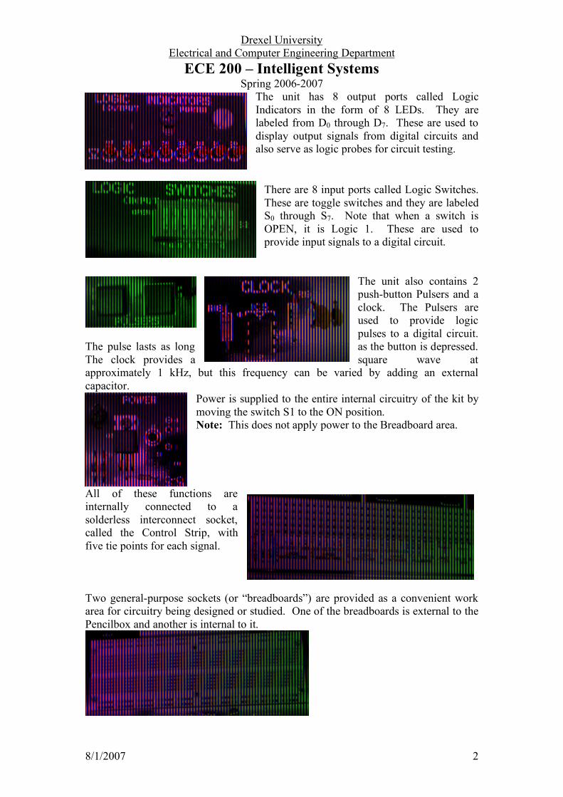
The unit has 8 output ports called Logic Indicators in the form of 8 LEDs. They are labeled from D0 through D7. These are used to display output signals from digital circuits and also serve as logic probes for circuit testing.
There are 8 input ports called Logic Switches. These are toggle switches and they are labeled S0 through S7. Note that when a switch is OPEN, it is Logic 1. These are used to provide input signals to a digital circuit.
The unit also contains 2 push-button Pulsers and a clock. The Pulsers are used to provide logic pulses to a digital circuit.
The pulse lasts as long as the button is depressed. The clock provides a square wave at approximately 1 kHz, but this frequency can be varied by adding an external capacitor.
Power is supplied to the entire internal circuitry of the kit by moving the switch S1 to the ON position. Note: This does not apply power to the Breadboard area.
All of these functions are internally connected to a solderless interconnect socket, called the Control Strip, with five tie points for each signal. Two general-purpose sockets (or “breadboards”) are provided as a convenient work area for circuitry being designed or studied. One of the breadboards is external to the Pencilbox and another is internal to it.
Drexel University Electrical and Computer Engineering Department
ECE 200 – Intelligent Systems Spring 2006-2007
8/1/2007 3
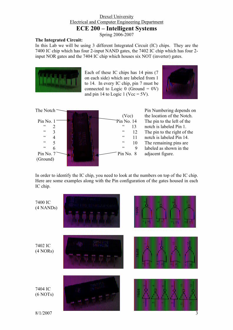
The Integrated Circuit: In this Lab we will be using 3 different Integrated Circuit (IC) chips. They are the 7400 IC chip which has four 2-input NAND gates, the 7402 IC chip which has four 2-input NOR gates and the 7404 IC chip which houses six NOT (inverter) gates.
Each of these IC chips has 14 pins (7 on each side) which are labeled from 1 to 14. In every IC chip, pin 7 must be connected to Logic 0 (Ground = 0V) and pin 14 to Logic 1 (Vcc = 5V).
The Notch Pin Numbering depends on (Vcc) the location of the Notch. Pin No. 1 Pin No. 14 The pin to the left of the “ 2 “ 13 notch is labeled Pin 1. “ 3 “ 12 The pin to the right of the “ 4 “ 11 notch is labeled Pin 14. “ 5 “ 10 The remaining pins are “ 6 “ 9 labeled as shown in the Pin No. 7 Pin No. 8 adjacent figure. (Ground) In order to identify the IC chip, you need to look at the numbers on top of the IC chip. Here are some examples along with the Pin configuration of the gates housed in each IC chip.
7400 IC (4 NANDs) 7402 IC (4 NORs) 7404 IC (6 NOTs)

Drexel University Electrical and Computer Engineering Department
ECE 200 – Intelligent Systems Spring 2006-2007
8/1/2007 4
Breadboarding Instructions: 1) Keep a wire cutter/stripper and a small screwdriver handy. 2) Generate a neat and complete circuit diagram on paper to help you guide with
the wiring. Every time you add a wire or component to the physical circuit, mark off the corresponding part of the wiring on your circuit diagram.
3) Before handling IC chips, discharge any electrostatic charge on your body by touching metal. Insert IC packages into the appropriate breadboard area before inserting any wires. You may need to bend the IC leads (pins) slightly inward so that the spacing closely matches the spacing of sockets on the breadboard. Be careful to check that all IC leads actually make it into the correct sockets.
4) To remove an IC, use an extraction tool, screwdriver, pliers or tweezers to avoid bending or breaking IC leads, or personal injury.
5) Use the connector wires available in the lab for wiring. Wire strippers may be used to cut wires to appropriate lengths.
6) Make sure the wires are not too thick (which could stretch the connector sockets) or too thin (which could result in unreliable or intermittent connections).
7) When removing wires, be sure to pull at a right angle to the socket to avoid damage.
8) Route wires around IC packages, not over them. Occasionally an IC turns out to be defective. If wires have been placed over the IC, you will have to remove them so that the IC can be replaced.
9) Wire a circuit in stages, beginning with power and ground connections. Add wires with the power switch OFF. Before turning power ON, make sure that no foreign metal objects are near the circuit.
10) Check every IC to make sure it is not overheating. If any IC is too hot to touch immediately shut the power off and check all leads. (Shorted ICs can become very hot!) Also make sure that no IC has been inserted backwards. IC devices can be damaged if the power level exceeds 5.5V. Damage may also occur if the supply voltage connection is removed from the IC pin while power is still being applied to the circuit.
11) To debug a circuit, use the logic indicator (L0 - L7) to check logic levels. Start at a position in the circuit where the logic level is known to be correct and work outward from there. If an IC does not appear to produce the correct signal, check that power and ground are correctly connected to the IC; also check all inputs to the component. Finally, check that the output of the IC is not incorrectly connected to some other signal.
Upper 2 rows The breadboard is divided into 2 halves, by a central channel. Perpendicular to upper half
this channel are many columns of five holes each. The five holes central channel
of each column are electrically connected together. They are not lower half
connected to any other part of the lab kit. A single column will be used to provide access to one pin of an IC. Lower two rows In addition, a breadboard has two upper rows and two lower rows (usually used for Logic 0 and Logic 1 connections). Note that each of these four rows has 50 holes; in
Drexel University Electrical and Computer Engineering Department
ECE 200 – Intelligent Systems Spring 2006-2007
8/1/2007 5
each row, the first 25 holes are electrically connected to each other, the next 25 holes are electrically connected to each other. The Control Panel:
1) The Control Strip (also called Control Panel) is located near the center of your kit. Similar to a breadboard, it has five rows; the five holes in each column are electrically connected together. The Control Strip contains connectors with labels such as “LOGIC INDICATORS”, “LOGIC SWITCHES” etc. It provides power and control signals to the circuit which will be built on the Breadboard area. A circuit is built on the breadboard by placing electrical components on the breadboard and attaching wires between the Control Strip and the Breadboard.
2) Before applying power to the kit, remove all metal objects from the vicinity of the kit. Move switch S1 to OFF position. Plug the AC adapter into a standard (120 VAC) wall outlet. Now move switch S1 to the ON position. This applies power to the internal circuitry of the kit only. No power is applied to the Breadboard area. Whenever you are finished working with the kit, move S1 to the OFF position before disconnecting the power.
3) Locate the connectors labeled “LOGIC 1, +5” and “LOGIC 0, GND” on the Control Strip (I). These are the power source for all of your devices. Be very careful when connecting wires to these areas. Although the voltage level is too low to be dangerous to you, sparks can result and you can easily damage the kit.
4) Locate the LOGIC INDICATOR connectors labeled L0 through L7 on the Control Strip. When a 5-volt signal is present at one of these connections, the corresponding LED is illuminated. Check out all of the LEDs in your kit by inserting a wire from one of LOGIC 1 power connectors to each of the LOGIC INDICATOR connectors in turn. Each LED should glow. Check these LEDs each time you work with your kit.
5) Locate the LOGIC SWITCHES connectors on the Control Strip: S0 through S7. These provide connections to 8 switches near the top of the kit. Connect switch S0 to an LED through the connection L0, and turn the switch ON and OFF a few times. Note which setting corresponds to a logic level 1 (the LED is on) and which corresponds to a logic level 0 (the LED is off). Make sure that all of the switches are functioning by testing each one in turn.
6) Power switch S1 should ALWAYS be OFF when inserting or removing ICs to prevent damage to the chips. Turn the power off and place one of the 7400 ICs near the center of the Breadboard area. VERY IMPORTANT: The two rows of pins of the IC should be on different sides of the central channel of the Breadboard. Push the IC so that each pin of the IC is inserted into a separate hole. There should now be four unused holes for each pin along the sides of the IC. Connections can be made to the IC through any of these exposed holes. Check the pin definitions (given in the previous section) and connect LOGIC 1 of the Control Panel to the VCC pin and LOGIC 0 to the GND pin. Again using the Control Panel, connect two Logic Switches to the input pins of one NAND gate. Connect the output of this NAND gate to one Logic Indicator. Verify that the NAND gate works properly by turning power ON and trying all

Drexel University Electrical and Computer Engineering Department
ECE 200 – Intelligent Systems Spring 2006-2007
8/1/2007 6
four possible switch settings and observing the LED. This is how you test each gate in an IC chip.
7) Now turn power OFF DC Voltage Measurements: You will be using the Hewlett Packard (HP) Multi-meter 34401A available in Rooms 7-204 and 7-206 to perform voltage measurements. This multi-meter can measure DC/AC voltages and currents, resistances, Period and Frequency. The parameter to be measured can be selected via the buttons on the Function Panel. You will need a pair (black and red) of 'Banana to Alligator' cables, which are available in Room 7-205. Turn on the Multi-meter by pressing the 'Power' button. Since you need to measure DC voltages, press the 'DC V' button on the Function Panel. There are two pairs of HI (red)-LO (black) terminals on the multi-meter. One HI-LO pair is on the left and the other HI-LO pair is on the right. In order to measure voltage, you will need the HI-LO terminal pair on the right (labeled ‘V’). Insert the banana end of the Red cable into this HI terminal. Insert the banana end of the Black cable into the corresponding LO terminal (just below the HI terminal). You are now ready to measure voltage. Let G be the ground pin on your IC chip and let O be the pin on the chip where you want to measure the voltage. Connect the alligator end on the Black cable to the Ground pin G of your IC chip via a connector wire. Connect the alligator end on the Red cable to the pin O on the chip via a connector wire. Record the voltage reading displayed on the multi-meter with the appropriate units. Remember that this voltage measurement indicates the voltage at pin O with respect to Ground.

Drexel University Electrical and Computer Engineering Department
ECE 200 – Intelligent Systems Spring 2006-2007
8/1/2007 7
Pre-Lab Exercise
Read the instructions in the previous sections of this manual. Pay careful attention to the lay-out of the pins on the IC chips, the connectors on the Control Panel, use of the light emitting diodes (LED’s), etc. Complete this form, get it signed by the Lab Assistant in Room 7-205 and turn it in with the Lab Report.
1) How many Logic Indicators does the unit have? Label them. ____________________________________________________________
2) How many Logic Switches does the unit have? Label them. ____________________________________________________________
3) When a switch is open, is it Logic 0 or Logic 1.___________ 4) Power Switch S1 supplies power to ____________________ 5) How many tie-points does each signal on the Control strip have?________ 6) What kind of gates does a 7400 IC chip have? How many?_____________ 7) What kind of gates does a 7402 IC chip have? How many?_____________ 8) What kind of gates does a 7404 IC chip have? How many?_____________ 9) How many pins do each of the above IC chips have?__________________ 10) How many Volts is Logic 0 and Logic 1? ___________________________ 11) In each of the above IC chip, which pin is Logic 0? Which pin is Logic
1?____________________ 12) Complete the following Truth Table
A B A NAND B A NOR B NOT A 0 0 0 1 1 0 1 1
13) Number all the output pins on the 7400 IC chip.______________________ 14) Number all the output pins on the 7402 IC chip.______________________ 15) Number all the output pins on the 7404 IC chip.______________________ 16) How many electrically connected holes does each column on the
breadboard have?______________ 17) A breadboard has 2 upper rows and 2 lower rows. Each row has 50 holes.
How many of these holes are electrically connected to each other? _______ 18) Have you carefully read and understood the entire handout?________ 19) Use the Breadboard simulation software (as seen in class) to wire an
NAND (7400) IC. The simulation software can be found on the CD with the book, or at the demo version at http://www.yoeric.com/breadboard.htm. For 1 NAND gate, step through all the possible states, and prove that the NAND chip works as expected. Provide a screen shot(s) that proves that the circuit is wired correctly and the chip is working
Group member names:______________________________________________
Lab assistant signature_____________________________ Date ____________

Drexel University Electrical and Computer Engineering Department
ECE 200 – Intelligent Systems Spring 2006-2007
8/1/2007 8
Lab Experimentation:
1) Test all the gates in the following IC chips and validate your results using the truth tables from your Pre-lab. Use the switches for the inputs into the ICs. To validate the truth tables, put the output of the chips to the LEDs. Use a data sheet that has enough space to record truth tables for gates on all chips. a) 7404 chip with six NOT gates (Inverters) b) 7402 chip with four 2-input NOR gates c) 7400 chip with four 2-input NAND gates
2) Use a voltmeter to measure the voltages corresponding to Logic 0 and Logic 1 at the output pin of each gate for the NOT, NOR, and NAND ICs. Comment on the voltage levels for a HIGH and LOW signal. a) Measure the voltage when the output pin of the gate is not connected to an
LED (Logic Indicator) b) Measure the voltage when the output pin of the gate is connected to an LED
(Logic indicator). From (a) and (b) notice and comment on the Loading effect introduced by the
LED in the circuit.
3) Use the voltmeter to measure the voltages at both the pins (touch a lead to each pin of the LED) of any one LED, which is ON (or lit up). Remember that these voltages are measured with respect to ground. Let these voltages be V1 and V2. The difference |V1 – V2| will be the voltage across the LED. Note down V1, V2 and VLED = |V1 – V2|.