Embed Size (px)
Citation preview
EconOscillator is a trademark of Maxim Integrated Products, Inc.
Add “/T” for Tape and Reel.Custom frequencies available, contact factory.
Pin Configuration and Typical Operating Circuits appear at end of data sheet.
General DescriptionThe DS1089L is a clock generator that produces a spread-spectrum (dithered) square-wave output of fre-quencies from 130kHz to 66.6MHz. The DS1089L is shipped from the factory programmed at a specific frequency. The DS1089L is pin-for-pin compatible with the DS1087L, however, the DS1089L dithers at equal percentages above and below the center frequency. The user still has access to the internal frequency divider, selectable ±1%, ±2%, ±4%, or ±8% dithered output, dith-ering rate, and programmable output power-down/disable mode through an I2C-compatible programming interface. All the device settings are stored in nonvolatile (NV) EEPROM allowing it to operate in stand-alone applica-tions. The DS1089L also has power-down and output-en-able control pins for power-sensitive applications.
Applications Printers Copiers Computer Peripherals POS Terminals Cable Modems
Features Factory-Programmed Square-Wave Generator from
33.3MHz to 66.6MHz Center Frequency Remains Constant Independent of
Dither Percentage No External Timing Components Required EMI Reduction Variable Dither Frequency User Programmable Down to 130kHz with Divider
(Dependent on Master Oscillator Frequency) ±1%, ±2%, ±4%, or ±8% Selectable Dithered Output Glitchless Output-Enable Control I2C-Compatible Serial Interface Nonvolatile Settings Power-Down Mode Programmable Output Power-Down/Disable Mode
19-7501; Rev 3; 2/15
PART FREQUENCY (MHz) SPREAD (±%) DITHER FREQUENCYDS1089LU-21G 14.7456 1 fMOSC/4096DS1089LU-4CL 18.432 2 fMOSC/4096DS1089LU-22F 24.576 1 fMOSC/2048DS1089LU-23C 33.3 1 fMOSC/4096DS1089LU-450 50.0 2 fMOSC/4096DS1089LU-866 66.6 4 fMOSC/4096DS1089LU-yxx Fixed up to 66.6 1, 2, 4, or 8 fMOSC/2048 or 4096 or 8192
*See Standard Frequency Options Table.
Ordering InformationPART TEMP RANGE PIN-PACKAGE
DS1089LU-yxx* -40°C to +85°C 8 µSOP (118 mil)
Standard Frequency Options
DS1089L 3.3V Center Spread-Spectrum EconOscillator™
Voltage on VCC Relative to Ground ....................-0.5V to +6.0VVoltage on SPRD, PDN, OE, SDA,
SCL Relative to Ground* ...................... -0.5V to (VCC + 0.5V)Operating Temperature Range ........................... -40°C to +85°C
Programming Temperature Range .........................0°C to +70°CStorage Temperature Range ............................ -55°C to +125°CSoldering Temperature ................. See IPC/JEDEC J-STD-020A
*This voltage must not exceed 6.0V.
(VCC = +2.7V to +3.6V, TA = -40°C to +85°C.)
(TA = -40°C to +85°C.)
PARAMETER SYMBOL CONDITION MIN TYP MAX UNITSHigh-Level Output Voltage (OUT) VOH IOH = -4mA, VCC = min 2.4 VLow-Level Output Voltage (OUT) VOL IOL = 4mA 0.4 V
Low-Level Output Voltage (SDA)VOL1 3mA sink current 0.4
VVOL2 6mA sink current 0.6
High-Level Input Current IIH VIH = VCC 1 µALow-Level Input Current IIL VIL = 0V -1 µASupply Current (Active) ICC CL = 15pF, fOUT = fMOSCmax 12 mAStandby Current (Power-Down) ICCQ Power-down mode 10 µA
PARAMETER SYMBOL CONDITION MIN TYP MAX UNITSSupply Voltage VCC (Note 1) 2.7 3.3 3.6 VHigh-Level Input Voltage(SDA, SCL, SPRD, PDN, OE)
VIH 0.7 x VCCVCC +
0.3 V
Low-Level Input Voltage(SDA, SCL, SPRD, PDN, OE)
VIL -0.3 0.3 x VCC
V
DC Electrical Characteristics
Recommended Operating Conditions
Stresses beyond those listed under “Absolute Maximum Ratings” may cause permanent damage to the device. These are stress ratings only, and functional operation of the device at these or any other conditions beyond those indicated in the operational sections of the specifications is not implied. Exposure to absolute maximum rating conditions for extended periods may affect device reliability.
Absolute Maximum Ratings
www.maximintegrated.com Maxim Integrated 2
DS1089L 3.3V Center Spread-Spectrum EconOscillator™
MOSC
MOSC
ff∆
MOSC
ff
∆
MOSC
ff
∆
(VCC = +2.7V to +3.6V, TA = -40°C to +85°C.)
(VCC = +2.7V to +3.6V, TA = -40°C to +85°C.)
PARAMETER SYMBOL CONDITION MIN TYP MAX UNITSFrequency Stable After PRESCALER Change 1 Period
Power-Up Time tPOR + tSTAB
(Note 6) 40 200 µs
Enable of OUT After Exiting Power-Down Mode tSTAB (Note 6) 512 clock
cycles
OUT Disabled After Entering Power-Down Mode tPDN 7 µs
Load Capacitance CL 15 50 pFOutput Duty Cycle (fOUT) 50 %
PARAMETER SYMBOL CONDITION MIN TYP MAX UNITS
Internal Master OscillatorFrequency fMOSC 33.3 66.6 MHz
Master Oscillator FrequencyTolerance
VCC = 3.3V,TA = +25°C (Notes 2, 10)
-0. 5 +0. 5 %
Voltage Frequency Variation TA = +25°C (Note 3) -0.75 +0.75 %
Temperature Frequency Variation(Note 4)
VCC = 3.3V,fOUT = fMOSCmax
TA = 0°C to +85°C -0.75 +0.75%
TA = -40°C to 0°C -2.00 +0.75
Dither Frequency Range(Note 5)
J3 = J2 = GND ±1
%J3 = GND, J2 = VCC ±2J3 = VCC, J2 = GND ±4J3 = J2 = VCC ±8
Dither Frequency(Note 5) fMOD
J1 = GND, J0 = VCC fMOSC / 2048HzJ1 = VCC, J0 = GND fMOSC / 4096
J1 = J0 = VCC fMOSC / 8192
AC Electrical Characteristics
Master Oscillator Characteristics
www.maximintegrated.com Maxim Integrated 3
DS1089L 3.3V Center Spread-Spectrum EconOscillator™
Note 1: All voltages are referenced to ground.Note 2: This is the absolute accuracy of the master oscillator frequency at the default settings with spread disabled.Note 3: This is the change that is observed in master oscillator frequency with changes in voltage at TA = +25°C.Note 4: This is the change that is observed in master oscillator frequency with changes in temperature at VCC = 3.3V.Note 5: The dither deviation of the master oscillator frequency is bidirectional and results in an output frequency centered at the
undithered frequency.Note 6: This indicates the time elapsed between power-up and the output becoming active. An on-chip delay is intentionally intro-
duced to allow the oscillator to stabilize. tSTAB is equivalent to 512 master clock cycles and will depend on the programmed master oscillator frequency.
Note 7: Timing shown is for fast-mode (400kHz) operation. This device is also backward compatible with I2C standard-mode timing.Note 8: CB—total capacitance of one bus line in picofarads.Note 9: EEPROM write time applies to all the EEPROM memory and SRAM shadowed EEPROM memory when WC = 0.
The EEPROM write time begins after a stop condition occurs.Note 10: Typical frequency shift due to aging is ±0.25%. Aging stressing includes Level 1 moisture reflow conditioning (24hr) +125°C
bake, 168hr +85°C/85°RH moisture soak, and three solder reflow passes +269 +0/-5°C peak) followed by 408hr max VCC biased 125°C HTOL, 500 temperature cycles at -55°C to +125°C, 96hr +130°C/85%RH/3,6V HAST and 168hr +121°C/2 ATM Steam/Unbiased Autoclave.
(VCC = +2.7V to +3.6V.)
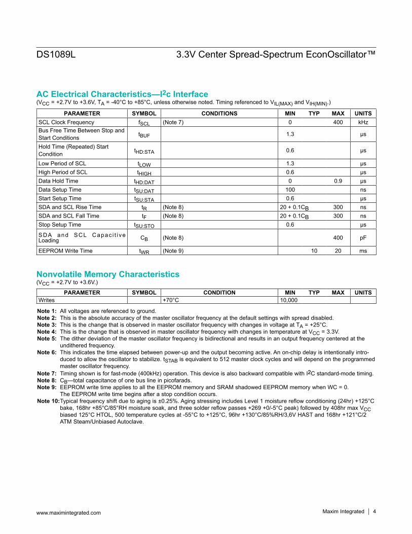
(VCC = +2.7V to +3.6V, TA = -40°C to +85°C, unless otherwise noted. Timing referenced to VIL(MAX) and VIH(MIN).)
PARAMETER SYMBOL CONDITION MIN TYP MAX UNITSWrites +70°C 10,000
PARAMETER SYMBOL CONDITIONS MIN TYP MAX UNITSSCL Clock Frequency fSCL (Note 7) 0 400 kHzBus Free Time Between Stop andStart Conditions tBUF 1.3 µs
Hold Time (Repeated) Start Condition tHD:STA 0.6 µs
Low Period of SCL tLOW 1.3 µsHigh Period of SCL tHIGH 0.6 µsData Hold Time tHD:DAT 0 0.9 µsData Setup Time tSU:DAT 100 nsStart Setup Time tSU:STA 0.6 µsSDA and SCL Rise Time tR (Note 8) 20 + 0.1CB 300 nsSDA and SCL Fall Time tF (Note 8) 20 + 0.1CB 300 nsStop Setup Time tSU:STO 0.6 µs
SDA and SCL Capac i t i ve Loading CB (Note 8) 400 pF
EEPROM Write Time tWR (Note 9) 10 20 ms
Nonvolatile Memory Characteristics
AC Electrical Characteristics—I2c Interface
www.maximintegrated.com Maxim Integrated 4
DS1089L 3.3V Center Spread-Spectrum EconOscillator™
(VCC = 3.3V, TA = +25°C, unless otherwise noted.)
-0.8
-0.6
-0.2
-0.4
0
0.2
-40 10-15 35 60 85
FREQUENCY % CHANGEvs. TEMPERATURE
DS 1
089L
toc0
6TEMPERATURE (ºC)
FREQ
UENC
Y CH
ANGE
(%)
66MHz50MHz
130kHz
33MHz
VCC = 3.3V
-0.50
-0.25
0
0.25
0.50
2.7 3.0 3.3 3.6
FREQUENCY % CHANGEvs. SUPPLY VOLTAGE
DS 1
089L
toc0
5
SUPPLY VOLTAGE (V)
FREQ
UENC
Y CH
ANGE
(%)
66MHz
50MHz
130kHz
33MHzTA = +25ºC
0
1
3
2
4
5
-40 10-15 35 60 85
SHUTDOWN SUPPLY CURRENTvs. TEMPERATURE
DS 1
089L
toc0
4
TEMPERATURE (ºC)
SUPP
LY C
URRE
NT (µ
A)
VCC = 3.3V,PDN = GND
01 100010010
SUPPLY CURRENTvs. PRESCALER
10
4
2
8
6
DS 1
089L
toc0
3
PRESCALE DIVIDER (DECIMAL)
SUPP
LY C
URRE
NT (m
A)
3.6V3.3V2.7V
TA = +25ºC,fMOSC = 50MHz,OUTPUT UNLOADED
0
3
2
1
4
5
6
7
8
9
10
-40 10-15 35 60 85
ACTIVE SUPPLY CURRENTvs. TEMPERATURE
DS 1
089L
toc0
2
TEMPERATURE (°C)
SUPP
LY C
URRE
NT (m
A)
66MHz
50MHz 130kHz33MHz
TA = +25ºC,OUTPUTUNLOADED
0
2
6
4
8
10
ACTIVE SUPPLY CURRENTvs. SUPPLY VOLTAGE
DS 1
089L
toc0
1
SUPPLY VOLTAGE (V)
SUPP
LY C
URRE
NT (m
A)
2.7 3.0 3.3 3.6
66MHz
50MHz 130kHz
33MHz
TA = +25ºC,OUTPUTUNLOADED
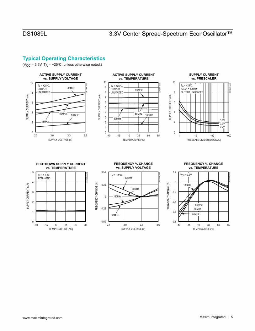
Typical Operating Characteristics
Maxim Integrated 5www.maximintegrated.com
DS1089L 3.3V Center Spread-Spectrum EconOscillator™
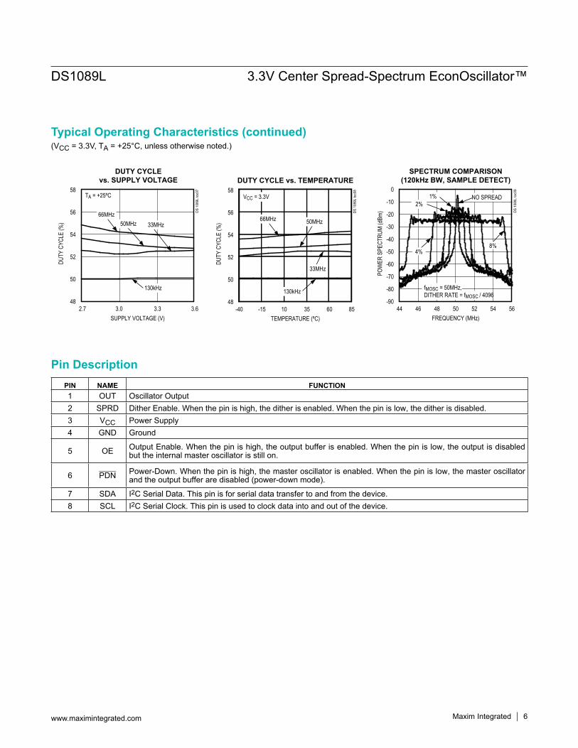
(VCC = 3.3V, TA = +25°C, unless otherwise noted.) Typical Operating Characteristics (continued)
PIN NAME FUNCTION1 OUT Oscillator Output2 SPRD Dither Enable. When the pin is high, the dither is enabled. When the pin is low, the dither is disabled.3 VCC Power Supply4 GND Ground
5 OE Output Enable. When the pin is high, the output buffer is enabled. When the pin is low, the output is disabled but the internal master oscillator is still on.
6 PDN Power-Down. When the pin is high, the master oscillator is enabled. When the pin is low, the master oscillator and the output buffer are disabled (power-down mode).
7 SDA I2C Serial Data. This pin is for serial data transfer to and from the device.8 SCL I2C Serial Clock. This pin is used to clock data into and out of the device.
48
50
54
52
56
58
DUTY CYCLEvs. SUPPLY VOLTAGE
DS 1
089L
toc0
7
SUPPLY VOLTAGE (V)
DUTY
CYC
LE (%
)
2.7 3.0 3.3 3.6
66MHz50MHz
130kHz
33MHz
TA = +25ºC
48
50
54
52
56
58
-40 10-15 35 60 85
DUTY CYCLE vs. TEMPERATURE
DS 1
089L
toc0
8
TEMPERATURE (ºC)
DUTY
CYC
LE (%
) 66MHz 50MHz
130kHz
33MHz
VCC = 3.3V
-90
-70
-80
-40
-50
-60
-10
-20
-30
0
44 4846 50 52 54 56
SPECTRUM COMPARISON(120kHz BW, SAMPLE DETECT)
DS 1
089L
toc0
9
FREQUENCY (MHz)
POW
ER S
PECT
RUM
(dBm
)
NO SPREAD1%2%
4%8%
fMOSC = 50MHz,DITHER RATE = fMOSC / 4096
Pin Description
www.maximintegrated.com Maxim Integrated 6
DS1089L 3.3V Center Spread-Spectrum EconOscillator™
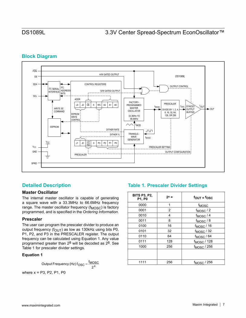
Detailed DescriptionMaster OscillatorThe internal master oscillator is capable of generating a square wave with a 33.3MHz to 66.6MHz frequency range. The master oscillator frequency (fMOSC) is factory programmed, and is specified in the Ordering Information.
PrescalerThe user can program the prescaler divider to produce an output frequency (fOUT) as low as 130kHz using bits P0, P1, P2, and P3 in the PRESCALER register. The output frequency can be calculated using Equation 1. Any value programmed greater than 28 will be decoded as 28. See Table 1 for prescaler divider settings.
Equation 1
MOSCOSC x
fOutput Frequency (Hz) f 2
=
where x = P3, P2, P1, P0
BITS P3, P2, P1, P0 2x = fOUT = fOSC
0000 1 fMOSC0001 2 fMOSC / 20010 4 fMOSC / 40011 8 fMOSC / 80100 16 fMOSC / 160101 32 fMOSC / 320110 64 fMOSC / 640111 128 fMOSC / 1281000 256 fMOSC / 256
1111 256 fMOSC / 256
Table 1. Prescaler Divider Settings
Block Diagram
FACTORY-PROGRAMMED
MASTEROSCILLATOR
33.3MHz TO66.6MHz
PRESCALER
DIVIDE BY 1, 2, 4,8, 16, 32, 64,128, OR 256
TRIANGLE-WAVE
GENERATOR
I2C SERIALINTERFACE
PRESCALER
ADDR
P0P1P2P3XLO/HIZ
J0J1
A0A1A2WCXOEJ2J3
VCC
VCC
SCL
SDA
DITHER RATE
DITHER %
EEPROM
WRITE EECOMMAND
OUT
I2CADDRESSBITS
PRESCALER SETTING
EEPROMWRITECONTROL
CONTROL REGISTERS
fMOD
fOSCfMOSC
fMOSC
fOUTSYNCEDOUTPUTBUFFER
OUTPUT CONFIGURATION
OUTPUT CONTROL
OE
PDN
GND
SPRD
S/W GATED OUTPUT
H/W GATED OUTPUTDS1089L
www.maximintegrated.com Maxim Integrated 7
DS1089L 3.3V Center Spread-Spectrum EconOscillator™
Output ControlTwo user control signals control the output. The output enable pin (OE) gates the output buffer and the pow-er-down pin (PDN) disables the master oscillator and turns off the output for power-sensitive applications. (Note: the power-down command must persist for at least two output frequency cycles plus 10µs for deglitching pur-poses.) On power-up, the output is disabled until power is stable and the master oscillator has generated 512 clock cycles.Additionally, the OE input is OR’ed with the OE bit in the ADDR register, allowing for either hardware or software gating of the output waveform (see the Block Diagram).Both controls feature a synchronous enable, which ensures that there are no output glitches when the output is enabled. The synchronous enable also ensures a con-stant time interval (for a given frequency setting) from an enable signal to the first output transition.
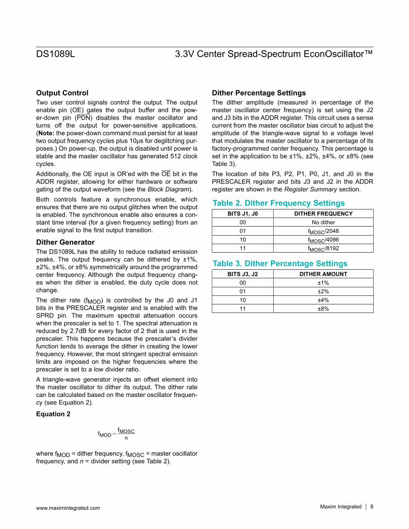
Dither GeneratorThe DS1089L has the ability to reduce radiated emission peaks. The output frequency can be dithered by ±1%, ±2%, ±4%, or ±8% symmetrically around the programmed center frequency. Although the output frequency chang-es when the dither is enabled, the duty cycle does not change.The dither rate (fMOD) is controlled by the J0 and J1 bits in the PRESCALER register and is enabled with the SPRD pin. The maximum spectral attenuation occurs when the prescaler is set to 1. The spectral attenuation is reduced by 2.7dB for every factor of 2 that is used in the prescaler. This happens because the prescaler’s divider function tends to average the dither in creating the lower frequency. However, the most stringent spectral emission limits are imposed on the higher frequencies where the prescaler is set to a low divider ratio.A triangle-wave generator injects an offset element into the master oscillator to dither its output. The dither rate can be calculated based on the master oscillator frequen-cy (see Equation 2).
Equation 2
MOSCMOD
ff n
=
where fMOD = dither frequency, fMOSC = master oscillator frequency, and n = divider setting (see Table 2).
Dither Percentage SettingsThe dither amplitude (measured in percentage of the master oscillator center frequency) is set using the J2 and J3 bits in the ADDR register. This circuit uses a sense current from the master oscillator bias circuit to adjust the amplitude of the triangle-wave signal to a voltage level that modulates the master oscillator to a percentage of its factory-programmed center frequency. This percentage is set in the application to be ±1%, ±2%, ±4%, or ±8% (see Table 3).The location of bits P3, P2, P1, P0, J1, and J0 in the PRESCALER register and bits J3 and J2 in the ADDR register are shown in the Register Summary section.
Table 2. Dither Frequency Settings
Table 3. Dither Percentage Settings
BITS J1, J0 DITHER FREQUENCY00 No dither01 fMOSC/204810 fMOSC/409611 fMOSC/8192
BITS J3, J2 DITHER AMOUNT00 ±1% 01 ±2%10 ±4%11 ±8%
www.maximintegrated.com Maxim Integrated 8
DS1089L 3.3V Center Spread-Spectrum EconOscillator™
X = “don’t care” x = values depend on custom settings
When dither is enabled (by selecting a dither frequency setting greater than 0 with SPRD high), the master oscil-lator frequency is dithered around the center frequency by the selected percentage from the programmed fMOSC (see Figure 2). For example, if fMOSC is programmed to 40MHz (factory setting) and the dither amount is programmed to ±1%, the frequency of fMOSC will dither between 39.6MHz and 40.4MHz at a modulation fre-quency determined by the selected dither frequency. Continuing with the same example, if J1 = 0 and J0 = 1, selecting fMOSC/2048, then the dither frequency would be 19.531kHz.
Register SummaryThe DS1089L registers are used to change the dith-er amount, output frequency, and slave address. A bit summary of the registers is shown in Table 4. Once programmed into EEPROM, the settings only need to be reprogrammed if it is desired to reconfigure the device.
PRESCALER RegisterBits 7 to 6: Dither Frequency. The J1 and J0 bits
control the dither frequency applied to the output. See Table 2 for divider settings. If either of bits J1 or J0 is high and SPRD is high, dither is enabled.
Bit 5: Output Low or Hi-Z. The LO/HIZ bit deter-mines the state of the output during pow-er-down. While the output is deactivated, if the LO/HIZ bit is set to 0, the output will be high impedance (high-Z). If the LO/HIZ bit is set to 1, the output will be driven low.
Bit 4: Reserved.Bits 3 to 0: Prescaler Divider. The prescaler bits (bits
P3 to P0) divide the master oscillator fre-quency by 2x where x can be from 0 to 8. Any prescaler bit value entered that is greater than 8 will decode as 8. See Table 1 for prescaler settings.
ADDR RegisterBits 7 to 6: Dither Percentage. The J3 and J2 bits con-
trol the selected dither amplitude (%). When both J3 and J2 are set to 0, the default dith-er rate is ±1%.
Bit 5: Output Enable. The OE bit and the OE pin state determine if the output is on when the device is active (PDN = VIH). If (OE = 0 OR OE is high) AND the PDN pin is high, the output will be driven.
Bit 4: Reserved.Bit 3: Write Control. The WC bit determines if
the EEPROM is to be written after register contents have been changed. If WC = 0 (default), EEPROM is written automatically after a write. If WC = 1, the EEPROM is only written when the WRITE EE command is issued. See the WRITE EE Command section for more information.
Bits 2 to 0: Address. The A0, A1, A2 bits determine the lower nibble of the I2C slave address.
Figure 2. Output Frequency vs. Dither Rate
Table 4. Register SummaryREGISTER ADDR BIT7 BINARY BIT0 DEFAULT ACCESS
PRESCALER 02h J1 J0 LO/ HIZ X P3 P2 P1 P0 xx00xxxxb R/W
ADDR 0Dh J3 J2 OE X WC A2 A1 A0 xx100000b R/W
WRITE EE 3Fh No Data — —
IF DITHER AMOUNT = 0%(+1, 2, 4,
OR 8% OF fMOSC)PROGRAMMED
fMOSC(-1, 2, 4,
OR 8% OF fMOSC)
DITHER AMOUNT(2, 4, 8, OR 16%)
TIME
1fMOD
f MOS
C
www.maximintegrated.com Maxim Integrated 9
DS1089L 3.3V Center Spread-Spectrum EconOscillator™
WRITE EE CommandThe WRITE EE command is useful in closed-loop appli-cations where the registers are frequently written. In applications where the register contents are frequently written, the WC bit should be set to 1 to prevent wearing out the EEPROM. Regardless of the value of the WC
bit, the value of the ADDR register is always written immediately to EEPROM. When the WRITE EE com-mand has been received, the contents of the registers are written into the EEPROM, thus locking in the register settings.
Figure 4. Slave Address Byte
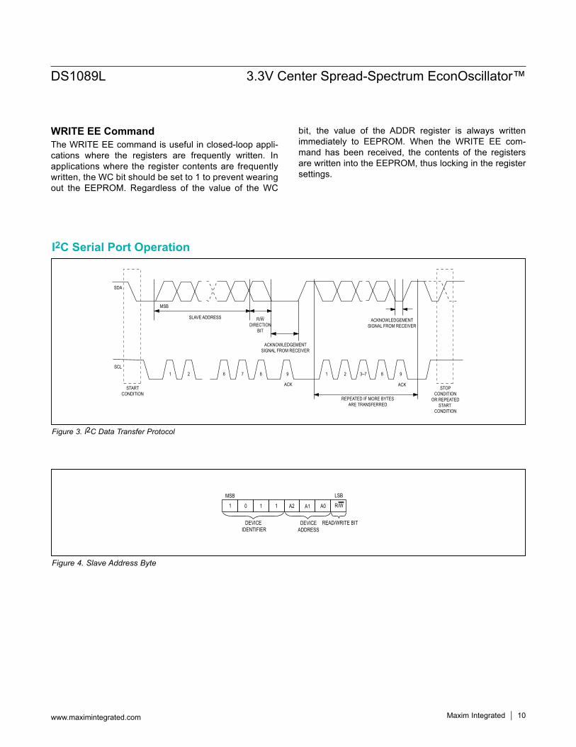
Figure 3. I2C Data Transfer Protocol
1 0 11 R/WA0A1A2
MSB LSB
DEVICE IDENTIFIER
DEVICEADDRESS
READ/WRITE BIT
STOPCONDITION
OR REPEATEDSTART
CONDITION
REPEATED IF MORE BYTESARE TRANSFERRED
ACKSTART
CONDITION
ACK
ACKNOWLEDGEMENTSIGNAL FROM RECEIVER
ACKNOWLEDGEMENTSIGNAL FROM RECEIVER
SLAVE ADDRESS
MSB
SCL
SDA
R/WDIRECTION
BIT
1 2 6 7 8 9 1 2 8 93–7
I2C Serial Port Operation
www.maximintegrated.com Maxim Integrated 10
DS1089L 3.3V Center Spread-Spectrum EconOscillator™
Applications InformationPower-Supply DecouplingTo achieve the best results when using the DS1089L, decouple the power supply with 0.01µF and 0.1µF high-quality, ceramic, surface-mount capacitors. Surface-mount components minimize lead inductance, which improves performance, and ceramic capacitors
tend to have adequate high-frequency response for decoupling applications. These capacitors should be placed as close to the VCC and GND pins as possible.
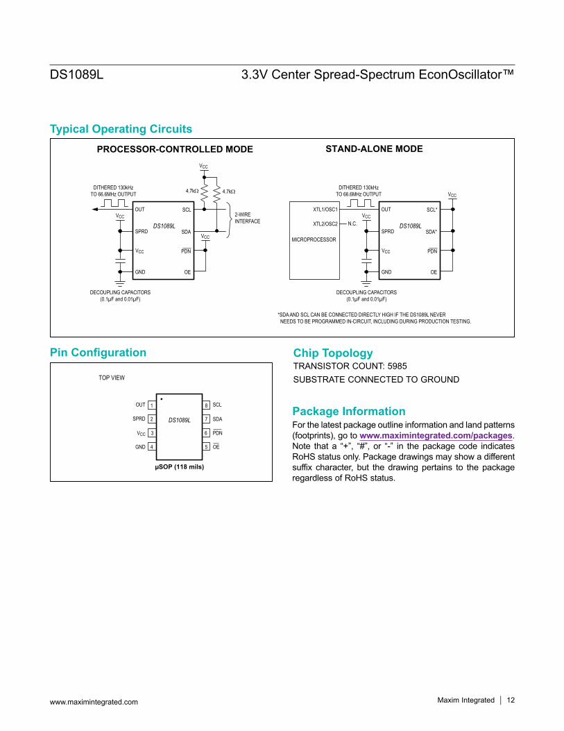
Stand-Alone ModeSCL and SDA cannot be left floating even in stand-alone mode. If the DS1089L will never need to be programmed in-circuit, including during production testing, SDA and SCL can be connected high.
Figure 5. I2C AC Characteristics
Figure 6. I2C Transactions
SDA
SCL
tHD:STA
tLOW
tHIGH
tR tF
tBUF
tHD:DAT
tSU:DAT REPEATEDSTART
tSU:STA
tHD:STA
tSU:STO
tSP
STOP START
SLAVEACK1 0 11 R/WA0*A1* SLAVE
ACKA2*MSB LSB
DEVICE IDENTIFIER DEVICEADDRESS
READ/WRITE
MSB LSB
COMMAND/REGISTER ADDRESS
SLAVEACK
MSB LSBb7 b6 b5 b4 b3 b2 b1 b0 SLAVE
ACK STOP
*THE ADDRESS DETERMINED BY A0, A1, AND A2 MUST MATCH THE ADDRESS SET IN THE ADDR REGISTER.
DATA
TYPICAL I2C WRITE TRANSACTION
EXAMPLE I2C TRANSACTIONS (WHEN A0, A1, AND A2 ARE ZERO)
A) SINGLE BYTE WRITE-WRITE PRESCALERREGISTER TO 128
B) SINGLE BYTE READ-READ PRESCALER REGISTER
START
START
START
B0h
B0h
SLAVEACK
SLAVEACK
02h
02hSLAVEACK
SLAVEACK
DATASLAVEACK STOP1 0 11 0 0 0 0
1 0 11 0 0 0 0
b7 b6 b5 b4 b3 b2 b1 b0
0 0 0 0 0 0 1 0 1 0 0 0 0 0 0 0
1 0 0 0 0 0 0 00 0 0 0 0 0 1 0 REPEATEDSTART
DATAMASTER
NACKSTOPSLAVE
ACK1 0 11 0 0 0 1
B1h
www.maximintegrated.com Maxim Integrated 11
DS1089L 3.3V Center Spread-Spectrum EconOscillator™
PDN
OEGND
1
2
8
7
SCL
SDASPRD
VCC
OUT
µSOP (118 mils)
TOP VIEW
3
4
6
5
DS1089L
STAND-ALONE MODEPROCESSOR-CONTROLLED MODE
OUT
SPRD
GND OE
PDN
SDA
SCL
VCC
VCC
VCC
VCC
4.7kΩ 4.7kΩ
2-WIREINTERFACE
DITHERED 130kHzTO 66.6MHz OUTPUT
DECOUPLING CAPACITORS(0.1µF and 0.01µF)
*SDA AND SCL CAN BE CONNECTED DIRECTLY HIGH IF THE DS1089L NEVER NEEDS TO BE PROGRAMMED IN-CIRCUIT, INCLUDING DURING PRODUCTION TESTING.
DS1089L
OUT
N.C.SPRD
GND OE
PDN
SDA*
SCL*
VCC
VCC
VCC
DITHERED 130kHzTO 66.6MHz OUTPUT
XTL2/OSC2
XTL1/OSC1
MICROPROCESSOR
DECOUPLING CAPACITORS(0.1µF and 0.01µF)
DS1089L
Package Information For the latest package outline information and land patterns (footprints), go to www.maximintegrated.com/packages. Note that a “+”, “#”, or “-” in the package code indicates RoHS status only. Package drawings may show a different suffix character, but the drawing pertains to the package regardless of RoHS status.
Chip TopologyTRANSISTOR COUNT: 5985SUBSTRATE CONNECTED TO GROUND
Pin Configuration
Typical Operating Circuits
www.maximintegrated.com Maxim Integrated 12
DS1089L 3.3V Center Spread-Spectrum EconOscillator™
REVISION NUMBER
REVISION DATE DESCRIPTION PAGES
CHANGED
2 5/06 —
3 2/15 Removed automotive reference from data sheet 1
Revision History
Maxim Integrated and the Maxim Integrated logo are trademarks of Maxim Integrated Products, Inc.
Maxim Integrated cannot assume responsibility for use of any circuitry other than circuitry entirely embodied in a Maxim Integrated product. No circuit patent licenses are implied. Maxim Integrated reserves the right to change the circuitry and specifications without notice at any time. The parametric values (min and max limits) shown in the Electrical Characteristics table are guaranteed. Other parametric values quoted in this data sheet are provided for guidance.
© 2015 Maxim Integrated Products, Inc. 13
DS1089L 3.3V Center Spread-Spectrum EconOscillator™
For pricing, delivery, and ordering information, please contact Maxim Direct at 1-888-629-4642, or visit Maxim Integrated’s website at www.maximintegrated.com.


![CR-1 : @TAWAS B LIB.TAWAS B(SCH 1):PAGE1 TAWASnotebookschematic.org/data/NOTEBOOK/attachments/SC... · resume gp[6] gp[7] gp[8] gp[9] 3.3v 3.3v 3.3v 3.3v gp[23] gp[24] gp[25] gp[26]](https://img.pdfslide.net/doc/110x75/5f812ff679030c23f20de0bd/cr-1-tawas-b-libtawas-bsch-1page1-ta-resume-gp6-gp7-gp8-gp9-33v.jpg)


![CONTENTS · Each LED is driven directly by ... PIN_F3 LED Green[5] 3.3V LED[6] PIN_B1 LED Green[6] 3.3V LED[7] PIN_L3 LED Green[7] 3.3V . …](https://img.pdfslide.net/doc/110x75/5b5b57cd7f8b9a55388e240b/contents-each-led-is-driven-directly-by-pinf3-led-green5-33v-led6.jpg)