Embed Size (px)
Citation preview
DSP Design Using MATLAB and Simulink with
Xilinx Targeted Design Platform
MathWorks and Xilinx joint Seminar
15 Sept. 2011
Daniele BagniXILINX DSP Specialist for EMEA
Copyright 2009 Xilinx
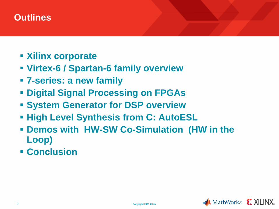
Outlines
Xilinx corporate
Virtex-6 / Spartan-6 family overview
7-series: a new family
Digital Signal Processing on FPGAs
System Generator for DSP overview
High Level Synthesis from C: AutoESL
Demos with HW-SW Co-Simulation (HW in the Loop)
Conclusion
2
Copyright 2009 Xilinx
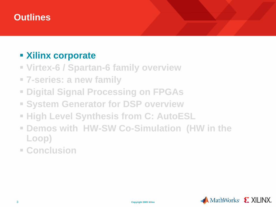
Outlines
Xilinx corporate
Virtex-6 / Spartan-6 family overview
7-series: a new family
Digital Signal Processing on FPGAs
System Generator for DSP overview
High Level Synthesis from C: AutoESL
Demos with HW-SW Co-Simulation (HW in the Loop)
Conclusion
3
Copyright 2009 Xilinx
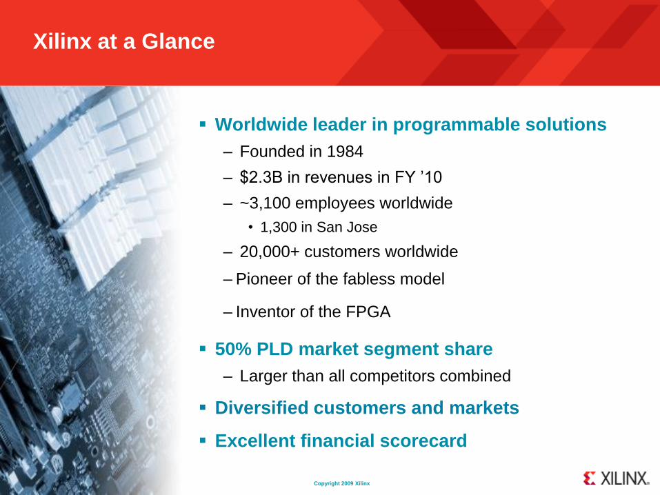
Worldwide leader in programmable solutions
– Founded in 1984
– $2.3B in revenues in FY ’10
– ~3,100 employees worldwide
• 1,300 in San Jose
– 20,000+ customers worldwide
– Pioneer of the fabless model
– Inventor of the FPGA
50% PLD market segment share
– Larger than all competitors combined
Diversified customers and markets
Excellent financial scorecard
Xilinx at a Glance
Copyright 2009 Xilinx5
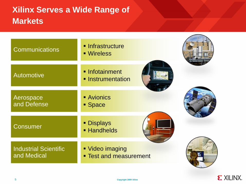
Xilinx Serves a Wide Range of
Markets
Avionics
SpaceAerospace and Defense
Infrastructure
WirelessCommunications
Infotainment
InstrumentationAutomotive
Displays
HandheldsConsumer
Video imaging
Test and measurementIndustrial Scientific and Medical
Copyright 2009 Xilinx
Outlines
Xilinx corporate
Virtex-6 / Spartan-6 family overview
7-series: a new family
Digital Signal Processing on FPGAs
System Generator for DSP overview
High Level Synthesis from C: AutoESL
Demos with HW-SW Co-Simulation (HW in the Loop)
Conclusion
6
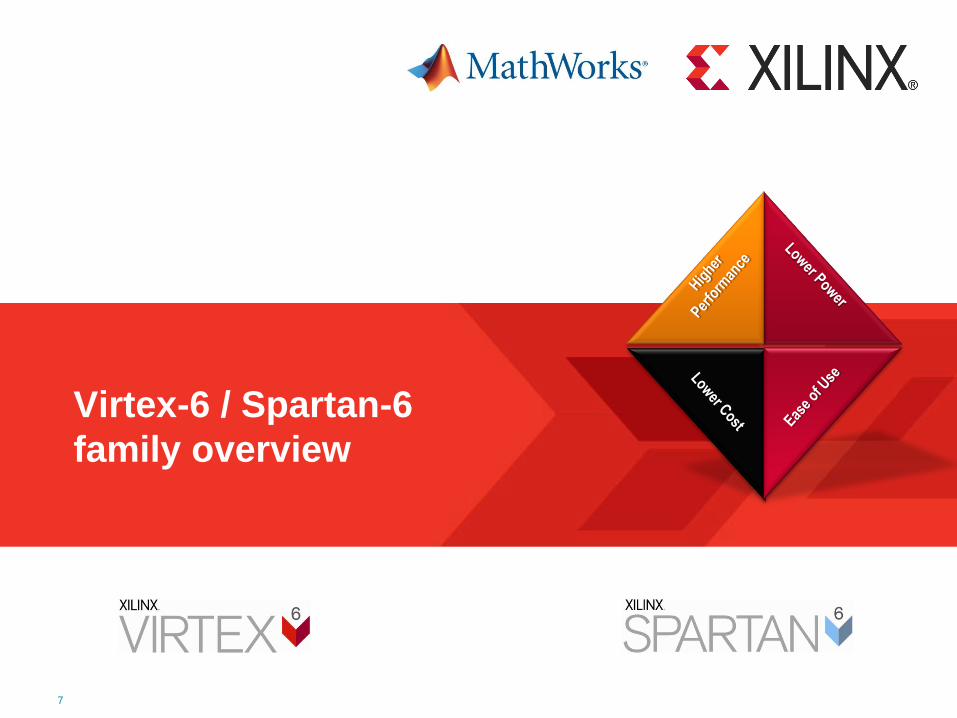
Virtex-6 / Spartan-6
family overview
7
Copyright 2009 Xilinx
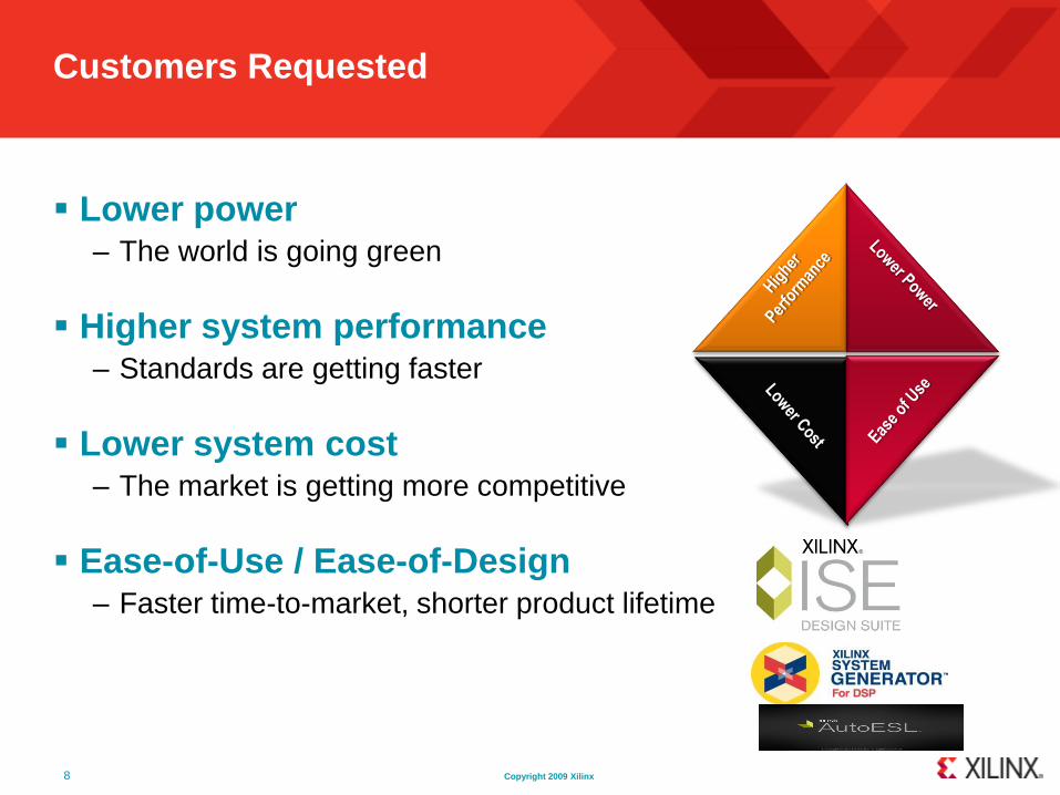
Customers Requested
Lower power– The world is going green
Higher system performance– Standards are getting faster
Lower system cost– The market is getting more competitive
Ease-of-Use / Ease-of-Design– Faster time-to-market, shorter product lifetime
8
Copyright 2009 Xilinx
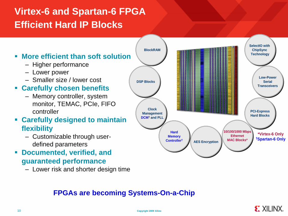
Virtex-6 and Spartan-6 FPGA
Efficient Hard IP Blocks
More efficient than soft solution– Higher performance
– Lower power
– Smaller size / lower cost
Carefully chosen benefits – Memory controller, system
monitor, TEMAC, PCIe, FIFO
controller
Carefully designed to maintain
flexibility– Customizable through user-
defined parameters
Documented, verified, and
guaranteed performance– Lower risk and shorter design time
FPGAs are becoming Systems-On-a-Chip
*Virtex-6 Only†Spartan-6 Only
DSP BlocksDSP BlocksLow-Power
Serial
Transceivers
Low-Power
Serial
Transceivers
SelectIO with
ChipSync
Technology
SelectIO with
ChipSync
TechnologyBlockRAMBlockRAM
10/100/1000 Mbps
Ethernet
MAC Blocks*
10/100/1000 Mbps
Ethernet
MAC Blocks*
Hard
Memory
Controller†
Hard
Memory
Controller†
Clock
Management
DCM† and PLL
Clock
Management
DCM† and PLL
PCI-Express
Hard Blocks
PCI-Express
Hard Blocks
AES EncryptionAES Encryption
DSP BlocksDSP BlocksDSP BlocksDSP BlocksLow-Power
Serial
Transceivers
Low-Power
Serial
Transceivers
Low-Power
Serial
Transceivers
Low-Power
Serial
Transceivers
SelectIO with
ChipSync
Technology
SelectIO with
ChipSync
Technology
SelectIO with
ChipSync
Technology
SelectIO with
ChipSync
TechnologyBlockRAMBlockRAMBlockRAMBlockRAM
10/100/1000 Mbps
Ethernet
MAC Blocks*
10/100/1000 Mbps
Ethernet
MAC Blocks*
10/100/1000 Mbps
Ethernet
MAC Blocks*
10/100/1000 Mbps
Ethernet
MAC Blocks*
Hard
Memory
Controller†
Hard
Memory
Controller†
Hard
Memory
Controller†
Hard
Memory
Controller†
Clock
Management
DCM† and PLL
Clock
Management
DCM† and PLL
Clock
Management
DCM† and PLL
Clock
Management
DCM† and PLL
PCI-Express
Hard Blocks
PCI-Express
Hard BlocksPCI-Express
Hard Blocks
PCI-Express
Hard Blocks
AES EncryptionAES EncryptionAES EncryptionAES Encryption
10
Copyright 2009 Xilinx
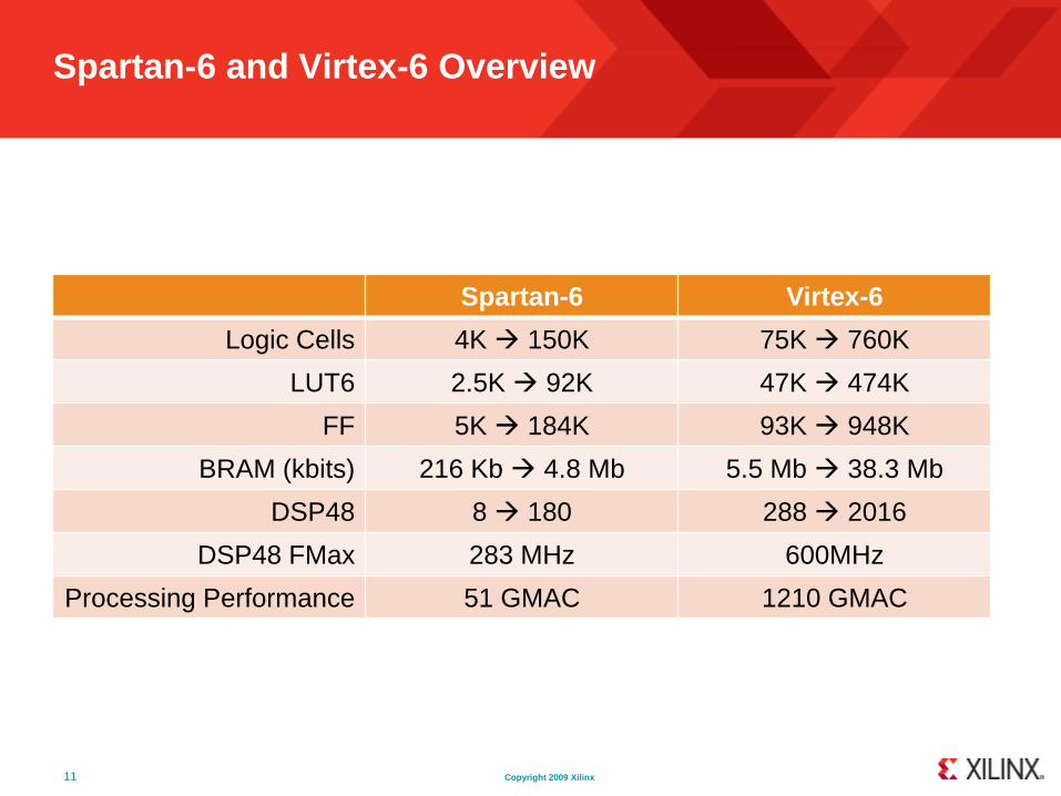
Spartan-6 and Virtex-6 Overview
Spartan-6 Virtex-6
Logic Cells 4K 150K 75K 760K
LUT6 2.5K 92K 47K 474K
FF 5K 184K 93K 948K
BRAM (kbits) 216 Kb 4.8 Mb 5.5 Mb 38.3 Mb
DSP48 8 180 288 2016
DSP48 FMax 283 MHz 600MHz
Processing Performance 51 GMAC 1210 GMAC
11
Copyright 2009 Xilinx
Outlines
Xilinx corporate
Virtex-6 / Spartan-6 family overview
7-series: a new family
Digital Signal Processing on FPGAs
System Generator for DSP overview
High Level Synthesis from C: AutoESL
Demos with HW-SW Co-Simulation (HW in the Loop)
Conclusion
12
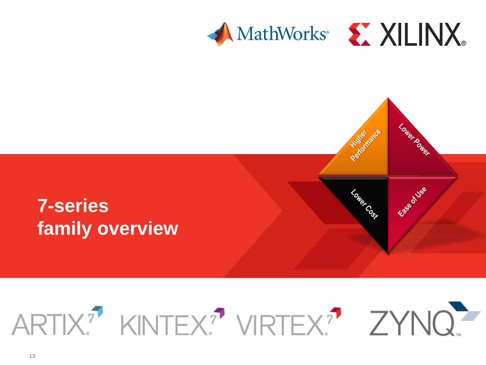
7-series
family overview
13
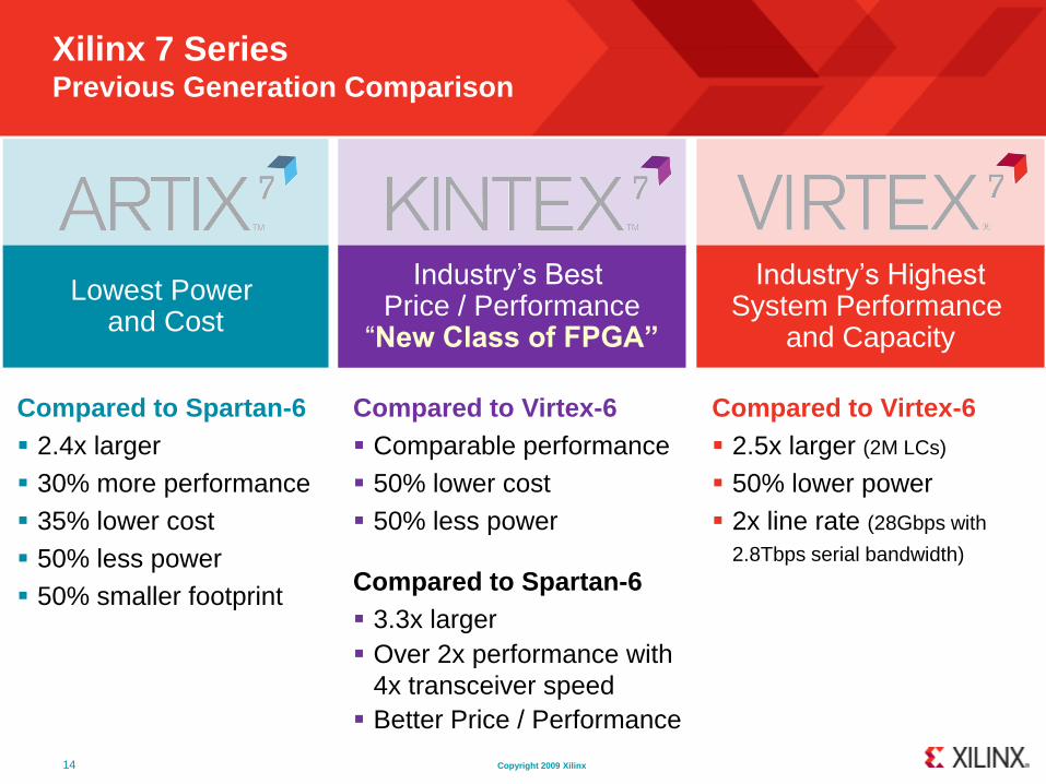
Copyright 2009 Xilinx
Xilinx 7 Series Previous Generation Comparison
Industry’s Best Price / Performance
“New Class of FPGA”
Compared to Virtex-6
Comparable performance
50% lower cost
50% less power
Compared to Spartan-6
3.3x larger
Over 2x performance with
4x transceiver speed
Better Price / Performance
Industry’s HighestSystem Performance
and Capacity
Compared to Virtex-6
2.5x larger (2M LCs)
50% lower power
2x line rate (28Gbps with
2.8Tbps serial bandwidth)
Lowest Power and Cost
Compared to Spartan-6
2.4x larger
30% more performance
35% lower cost
50% less power
50% smaller footprint
14
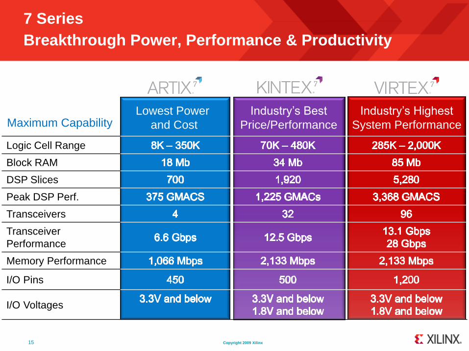
Copyright 2009 Xilinx
Logic Cell Range
Block RAM
DSP Slices
Peak DSP Perf.
Transceivers
Transceiver
Performance
Memory Performance
I/O Pins
I/O Voltages
Lowest Power
and Cost
Industry’s Best
Price/Performance
Industry’s Highest
System Performance
7 Series
Breakthrough Power, Performance & Productivity
Maximum Capability
15
Copyright 2009 Xilinx
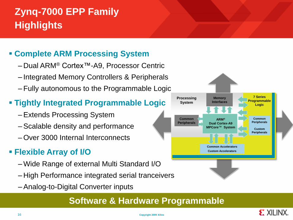
Zynq-7000 EPP Family
Highlights
Software & Hardware Programmable
7 Series
Programmable
Logic
Common
Peripherals
Custom
Peripherals
Common Accelerators
Custom Accelerators
Common
Peripherals
Processing
System
Memory
Interfaces
ARM®
Dual Cortex-A9
MPCore™ System
Complete ARM Processing System
– Dual ARM® Cortex™-A9, Processor Centric
– Integrated Memory Controllers & Peripherals
– Fully autonomous to the Programmable Logic
Tightly Integrated Programmable Logic
– Extends Processing System
– Scalable density and performance
– Over 3000 Internal Interconnects
Flexible Array of I/O
– Wide Range of external Multi Standard I/O
– High Performance integrated serial tranceivers
– Analog-to-Digital Converter inputs
16
Copyright 2009 Xilinx
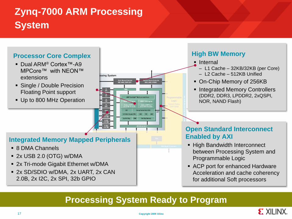
Zynq-7000 ARM Processing
System
Integrated Memory Mapped Peripherals
8 DMA Channels
2x USB 2.0 (OTG) w/DMA
2x Tri-mode Gigabit Ethernet w/DMA
2x SD/SDIO w/DMA, 2x UART, 2x CAN 2.0B, 2x I2C, 2x SPI, 32b GPIO
High BW Memory
Internal– L1 Cache – 32KB/32KB (per Core)– L2 Cache – 512KB Unified
On-Chip Memory of 256KB
Integrated Memory Controllers (DDR2, DDR3, LPDDR2, 2xQSPI, NOR, NAND Flash)
Processor Core Complex
Dual ARM® Cortex™-A9 MPCore™ with NEON™ extensions
Single / Double Precision Floating Point support
Up to 800 MHz Operation
Open Standard Interconnect Enabled by AXI
High Bandwidth Interconnect between Processing System and Programmable Logic
ACP port for enhanced Hardware Acceleration and cache coherency for additional Soft processors
Processing System Ready to Program
17
Copyright 2009 Xilinx
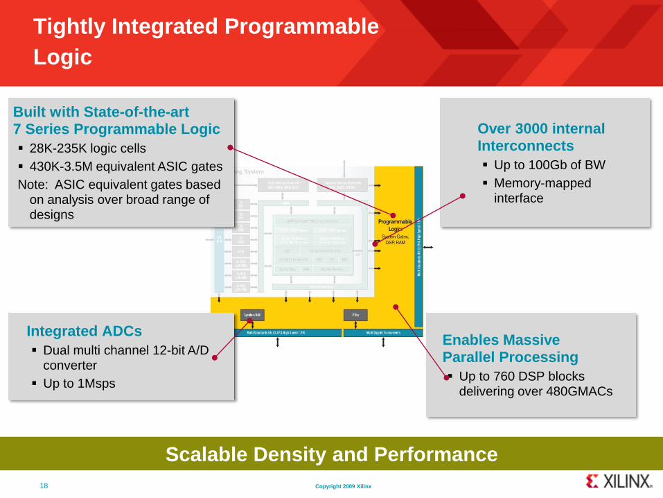
Tightly Integrated Programmable
Logic
Scalable Density and Performance
Over 3000 internal Interconnects
Up to 100Gb of BW
Memory-mapped interface
Built with State-of-the-art 7 Series Programmable Logic
28K-235K logic cells
430K-3.5M equivalent ASIC gates
Note: ASIC equivalent gates based on analysis over broad range of designs
Enables Massive Parallel Processing
Up to 760 DSP blocks delivering over 480GMACs
Integrated ADCs
Dual multi channel 12-bit A/D converter
Up to 1Msps
18
Copyright 2009 Xilinx
Outlines
Xilinx corporate
Virtex-6 / Spartan-6 family overview
7-series: a new family
Digital Signal Processing on FPGAs
System Generator for DSP overview
High Level Synthesis from C: AutoESL
Demos with HW-SW Co-Simulation (HW in the Loop)
Conclusion
19
DSP on FPGAs
Copyright 2009 Xilinx
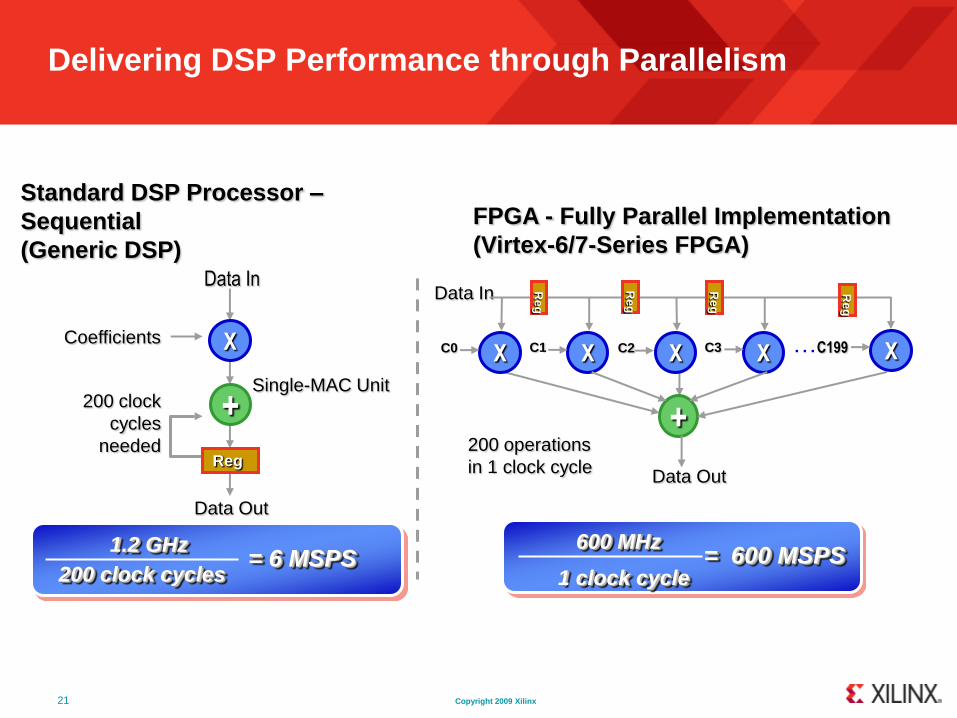
Delivering DSP Performance through Parallelism
Data Out
Single-MAC Unit
Coefficients
1.2 GHz
200 clock cycles= 6 MSPS
200 clock
cycles
needed
Data In
X
+
Reg
600 MHz
1 clock cycle= 600 MSPS
Data Out
FPGA - Fully Parallel Implementation
(Virtex-6/7-Series FPGA)
200 operations
in 1 clock cycle
Data In
X
+
C0 C0XC1 XC2 XC3 XC199…
Re
g
Re
g
Re
g
Re
g
Standard DSP Processor –
Sequential
(Generic DSP)
21
Copyright 2009 Xilinx22
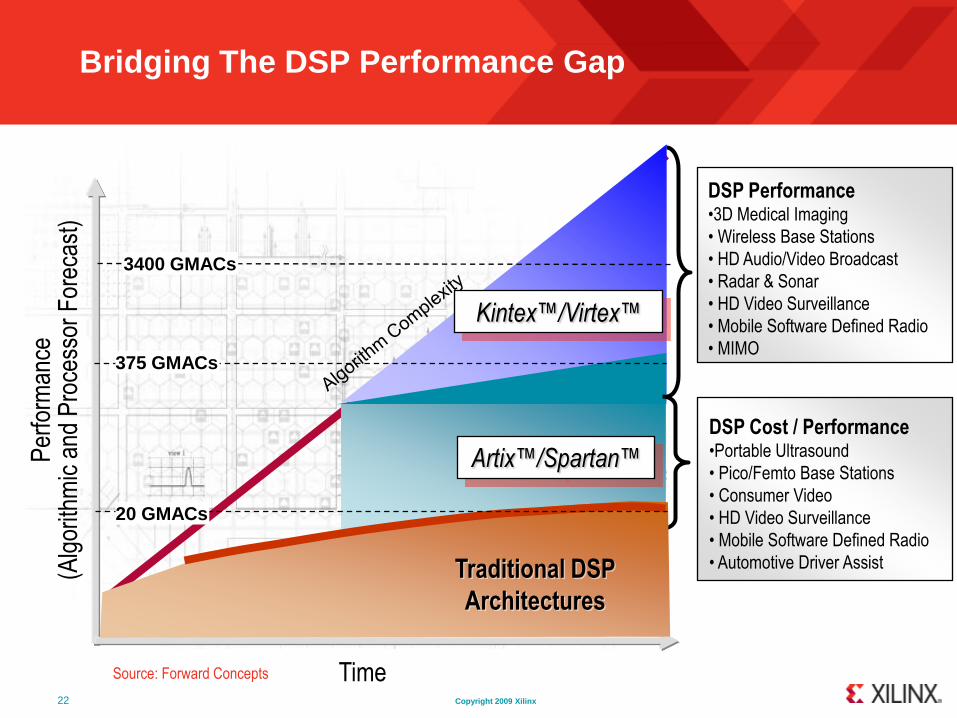
Bridging The DSP Performance GapP
erfo
rman
ce(A
lgor
ithm
ic a
nd P
roce
ssor
For
ecas
t)
Time
DSP Performance •3D Medical Imaging
• Wireless Base Stations
• HD Audio/Video Broadcast
• Radar & Sonar
• HD Video Surveillance
• Mobile Software Defined Radio
• MIMO
Source: Forward Concepts
Kintex™/Virtex™
Artix™/Spartan™
DSP Cost / Performance •Portable Ultrasound
• Pico/Femto Base Stations
• Consumer Video
• HD Video Surveillance
• Mobile Software Defined Radio
• Automotive Driver Assist
20 GMACs
375 GMACs
3400 GMACs
Traditional DSP
Architectures
Copyright 2009 Xilinx
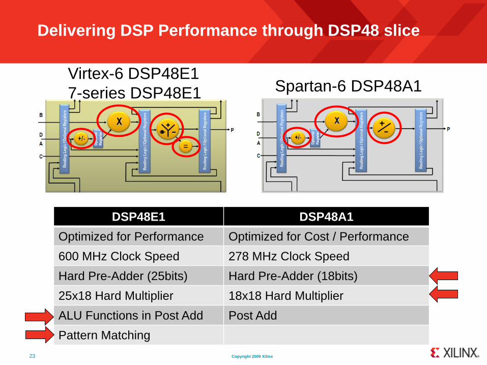
Delivering DSP Performance through DSP48 slice
Virtex-6 DSP48E1
7-series DSP48E1 Spartan-6 DSP48A1
DSP48E1 DSP48A1
Optimized for Performance Optimized for Cost / Performance
600 MHz Clock Speed 278 MHz Clock Speed
Hard Pre-Adder (25bits) Hard Pre-Adder (18bits)
25x18 Hard Multiplier 18x18 Hard Multiplier
ALU Functions in Post Add Post Add
Pattern Matching
23
Copyright 2009 Xilinx
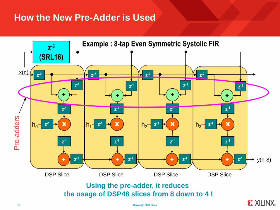
How the New Pre-Adder is Used
z-2 z-2 z-2
z-1 z-1
z-2
z-1
x(n)
+ + + +
X X X Xh0 h1 h2 h3
+ + + + y(n-8)
z-1
z-1 z-1 z-1 z-1
z-1 z-1 z-1 z-1
z-1
z-1
z-1
z-1
z-1
z-1
z-1
z-1
z-8
(SRL16)
DSP Slice DSP Slice DSP Slice DSP Slice
Example : 8-tap Even Symmetric Systolic FIR
Using the pre-adder, it reduces
the usage of DSP48 slices from 8 down to 4 !
Pre
-adders
24
Copyright 2009 Xilinx
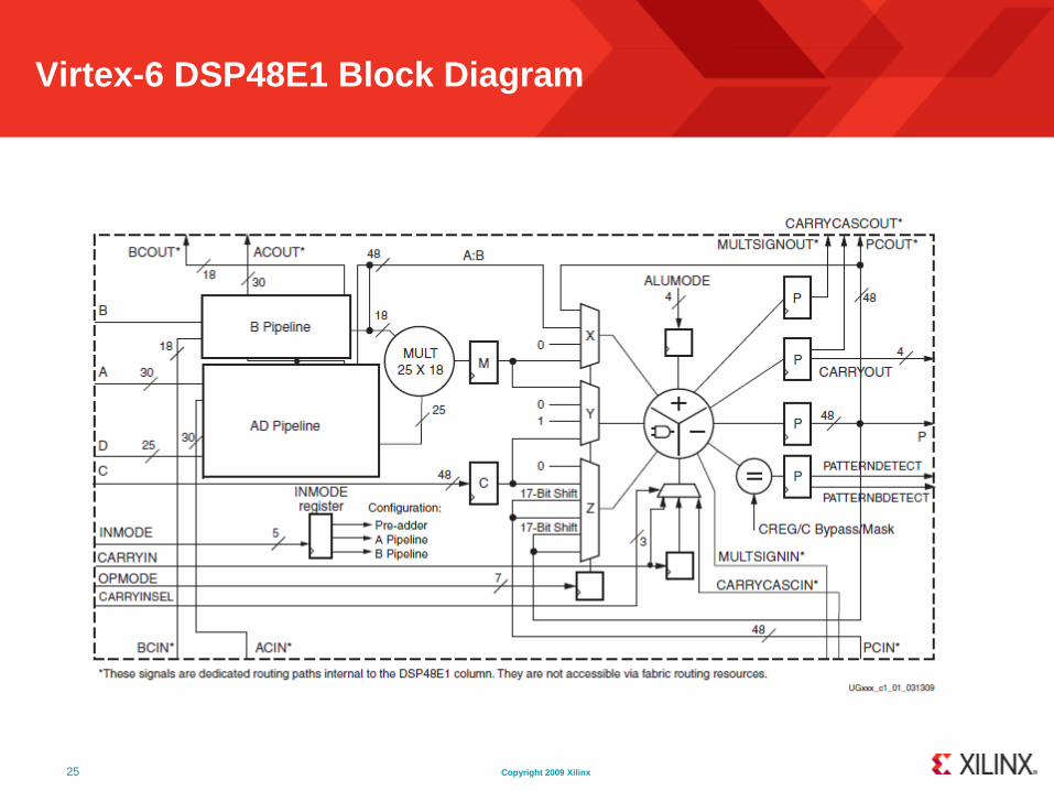
Virtex-6 DSP48E1 Block Diagram
25

Copyright 2009 Xilinx
Outlines
Xilinx corporate
Virtex-6 / Spartan-6 family overview
7-series: a new family
Digital Signal Processing on FPGAs
System Generator for DSP overview
High Level Synthesis from C: AutoESL
Demos with HW-SW Co-Simulation (HW in the Loop)
Conclusion
27
System Generator for DSP
28
Copyright 2009 Xilinx
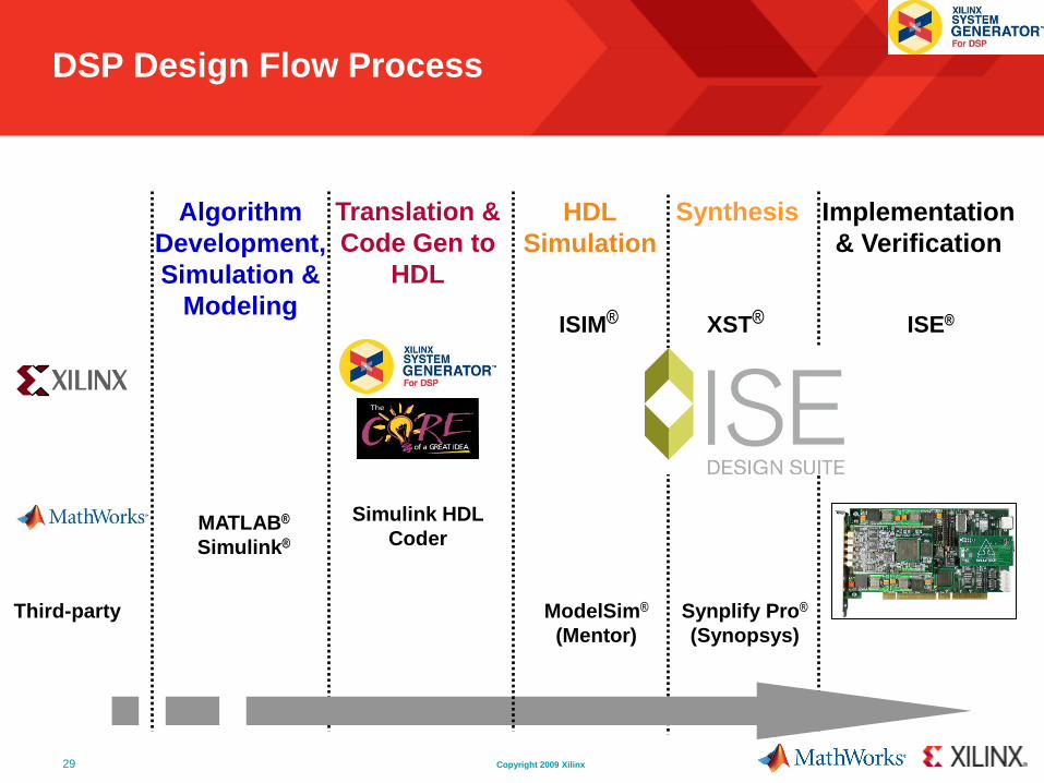
Algorithm
Development,
Simulation &
Modeling
MATLAB®
Simulink®
Synthesis
XST®
Synplify Pro®
(Synopsys)
HDL
Simulation
ModelSim®
(Mentor)
ISIM®
Implementation
& Verification
ISE®
Translation &
Code Gen to
HDL
DSP Design Flow Process
29
Simulink HDL
Coder
Third-party
Copyright 2009 Xilinx
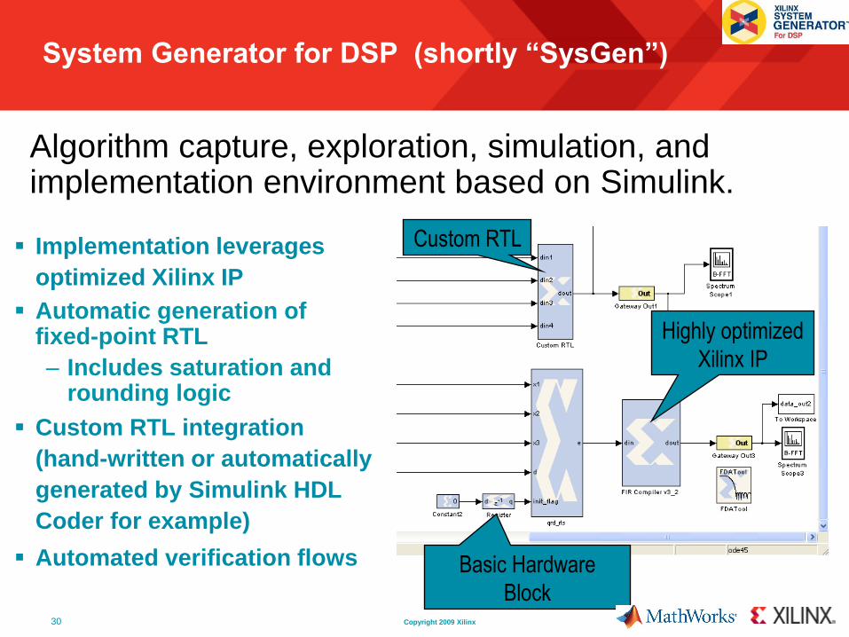
System Generator for DSP (shortly “SysGen”)
Implementation leverages
optimized Xilinx IP
Automatic generation of fixed-point RTL
– Includes saturation and rounding logic
Custom RTL integration
(hand-written or automatically
generated by Simulink HDL
Coder for example)
Automated verification flows
Algorithm capture, exploration, simulation, and implementation environment based on Simulink.
Custom RTL
Basic Hardware
Block
Highly optimized
Xilinx IP
30
Copyright 2009 Xilinx
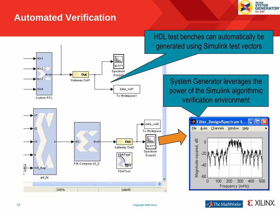
Automated Verification
System Generator leverages the
power of the Simulink algorithmic
verification environment
HDL test benches can automatically be
generated using Simulink test vectors
31
Copyright 2009 Xilinx
SysGen usage
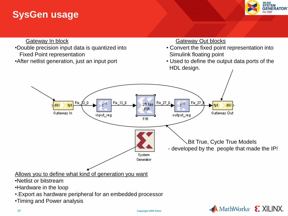
Gateway In block
•Double precision input data is quantized into
Fixed Point representation
•After netlist generation, just an input port
Gateway Out blocks
• Convert the fixed point representation into
Simulink floating point
• Used to define the output data ports of the
HDL design.
Allows you to define what kind of generation you want
•Netlist or bitstream
•Hardware in the loop
•.Export as hardware peripheral for an embedded processor
•Timing and Power analysis
Bit True, Cycle True Models
- developed by the people that made the IP!
32
Copyright 2009 Xilinx
Design optimization using SysGen blocks
Examples
DSP Macro
– Select operations to use
– Choose which register stage to implement
– Specify dedicated routing
BRAM
– Specify type: Distributed RAM or BRAM
– Indicate depth, latency
– Specify bitwidth on the different ports
– Provide reset and enable ports
– Select Write mode: read after write, read before write, no read on write
FFT
– Choose architecture: pipeline streaming IO, radix 2/4 burst IO
– Bitwidth
– BRAM usage
33
Copyright 2009 Xilinx
Outlines
Xilinx corporate
Virtex-6 / Spartan-6 family overview
7-series: a new family
Digital Signal Processing on FPGAs
System Generator for DSP overview
High Level Synthesis from C: AutoESL
Demos with HW-SW Co-Simulation (HW in the Loop)
Conclusion
37
Introduction to Xilinx
High Level Synthesis (HLS)
Daniele Bagni ([email protected])
EMEA DSP Specialist FAE
38
Copyright 2009 Xilinx
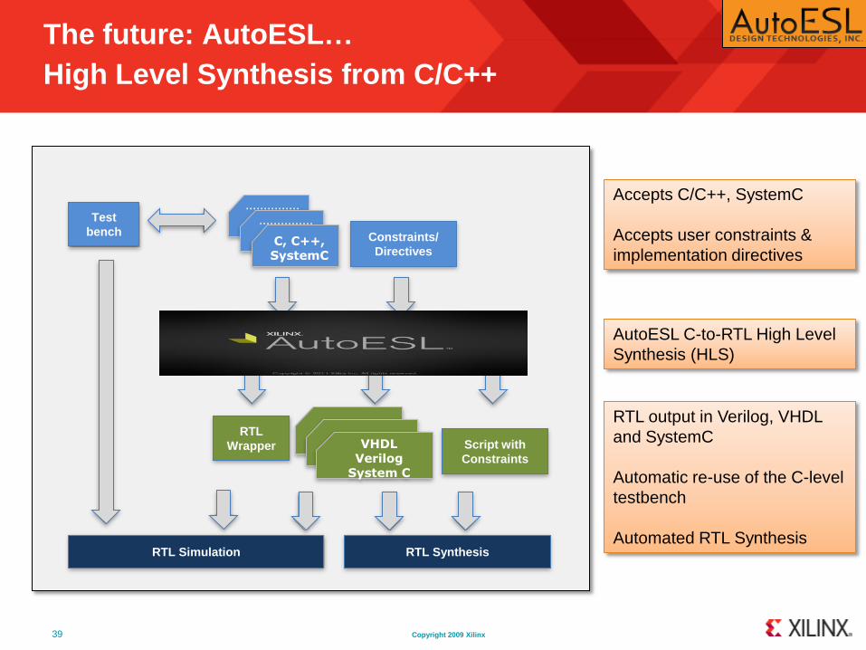
The future: AutoESL…
High Level Synthesis from C/C++
Script with
Constraints
RTL
Wrapper
………………………………VHDL
VerilogSystem C
AutoPilot
Test
bench Constraints/
Directives
………………………………C, C++,
SystemC
RTL Simulation RTL Synthesis
Accepts C/C++, SystemC
Accepts user constraints &
implementation directives
AutoESL C-to-RTL High Level
Synthesis (HLS)
RTL output in Verilog, VHDL
and SystemC
Automatic re-use of the C-level
testbench
Automated RTL Synthesis
39
Copyright 2009 Xilinx
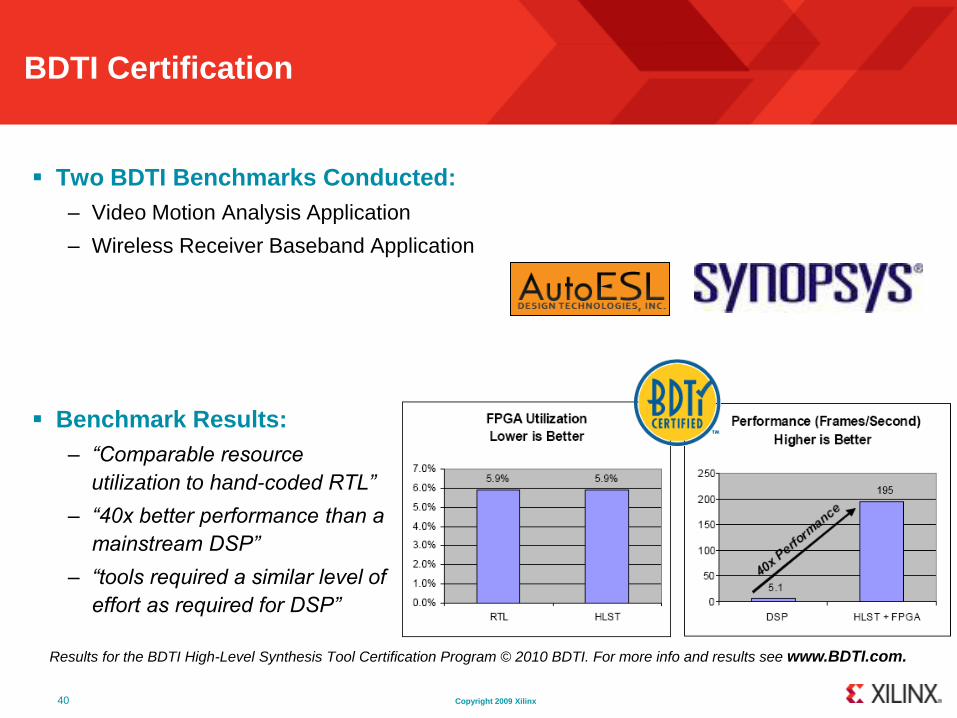
BDTI Certification
Two BDTI Benchmarks Conducted:
– Video Motion Analysis Application
– Wireless Receiver Baseband Application
Results for the BDTI High-Level Synthesis Tool Certification Program © 2010 BDTI. For more info and results see www.BDTI.com.
Benchmark Results:
– “Comparable resource
utilization to hand-coded RTL”
– “40x better performance than a
mainstream DSP”
– “tools required a similar level of
effort as required for DSP”
40
Copyright 2009 Xilinx
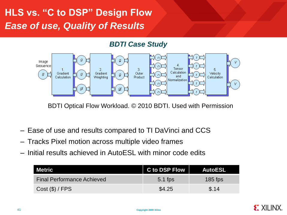
HLS vs. “C to DSP” Design Flow
Ease of use, Quality of Results
– Ease of use and results compared to TI DaVinci and CCS
– Tracks Pixel motion across multiple video frames
– Initial results achieved in AutoESL with minor code edits
41
Metric C to DSP Flow AutoESL
Final Performance Achieved 5.1 fps 185 fps
Cost ($) / FPS $4.25 $.14
BDTI Case Study
BDTI Optical Flow Workload. © 2010 BDTI. Used with Permission
Copyright 2009 Xilinx
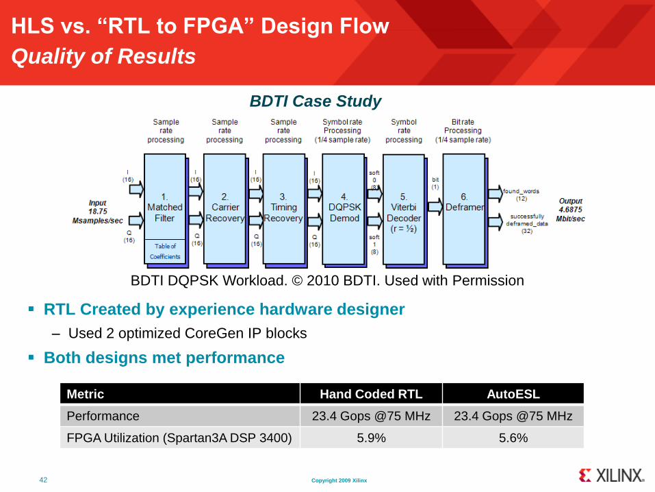
HLS vs. “RTL to FPGA” Design Flow
Quality of Results
42
RTL Created by experience hardware designer
– Used 2 optimized CoreGen IP blocks
Both designs met performance
Metric Hand Coded RTL AutoESL
Performance 23.4 Gops @75 MHz 23.4 Gops @75 MHz
FPGA Utilization (Spartan3A DSP 3400) 5.9% 5.6%
BDTI Case Study
BDTI DQPSK Workload. © 2010 BDTI. Used with Permission
Copyright 2009 Xilinx
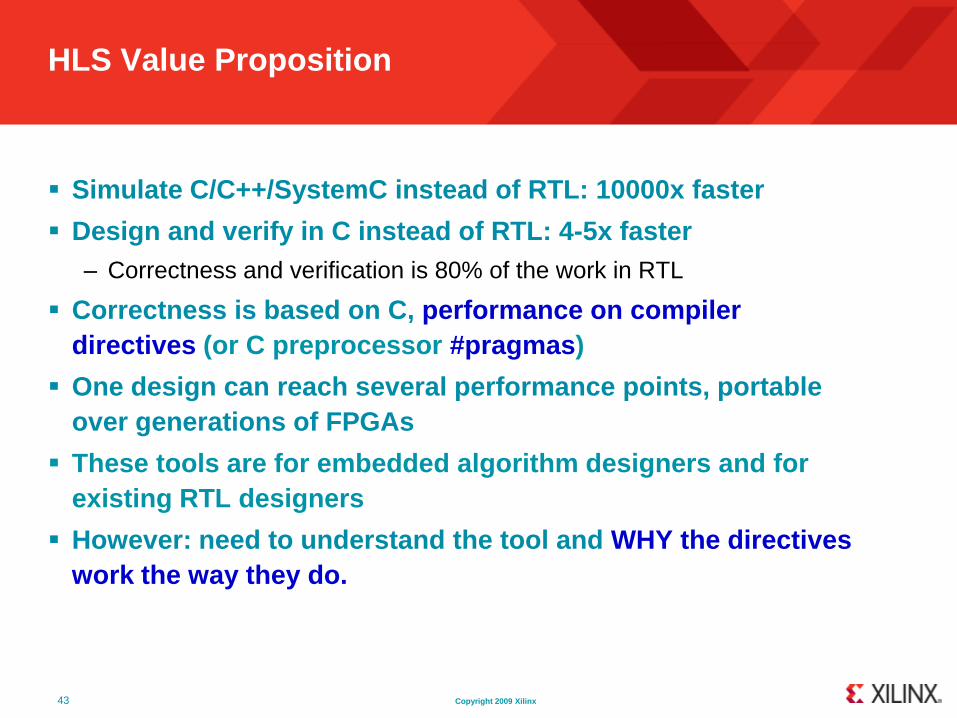
HLS Value Proposition
Simulate C/C++/SystemC instead of RTL: 10000x faster
Design and verify in C instead of RTL: 4-5x faster
– Correctness and verification is 80% of the work in RTL
Correctness is based on C, performance on compiler
directives (or C preprocessor #pragmas)
One design can reach several performance points, portable
over generations of FPGAs
These tools are for embedded algorithm designers and for
existing RTL designers
However: need to understand the tool and WHY the directives
work the way they do.
43
Copyright 2009 Xilinx
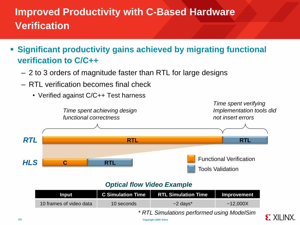
Improved Productivity with C-Based Hardware
Verification
Significant productivity gains achieved by migrating functional
verification to C/C++
– 2 to 3 orders of magnitude faster than RTL for large designs
– RTL verification becomes final check
• Verified against C/C++ Test harness
RTL RTL
C RTLFunctional Verification
Tools Validation
Time spent achieving design
functional correctness
Time spent verifying
Implementation tools did
not insert errors
Input C Simulation Time RTL Simulation Time Improvement
10 frames of video data 10 seconds ~2 days* ~12,000X
Optical flow Video Example
* RTL Simulations performed using ModelSim
RTL
HLS
44
Copyright 2009 Xilinx
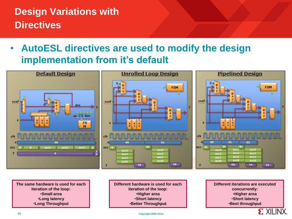
Design Variations with
Directives
• AutoESL directives are used to modify the design
implementation from it’s default
The same hardware is used for each
iteration of the loop:
•Small area
•Long latency
•Long Throughput
Different hardware is used for each
iteration of the loop:
•Higher area
•Short latency
•Better Throughput
Different iterations are executed
concurrently:
•Higher area
•Short latency
•Best throughput
45
Copyright 2009 Xilinx
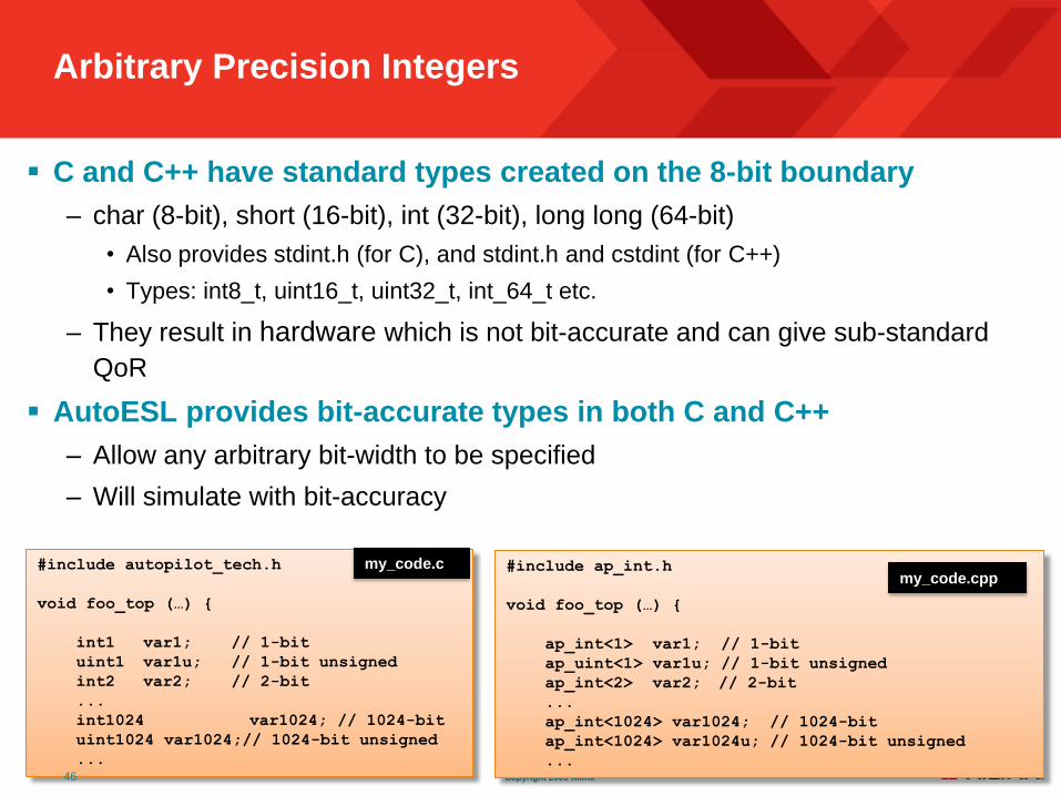
Arbitrary Precision Integers
C and C++ have standard types created on the 8-bit boundary
– char (8-bit), short (16-bit), int (32-bit), long long (64-bit)
• Also provides stdint.h (for C), and stdint.h and cstdint (for C++)
• Types: int8_t, uint16_t, uint32_t, int_64_t etc.
– They result in hardware which is not bit-accurate and can give sub-standard
QoR
AutoESL provides bit-accurate types in both C and C++
– Allow any arbitrary bit-width to be specified
– Will simulate with bit-accuracy
#include autopilot_tech.h
void foo_top (…) {
int1 var1; // 1-bit
uint1 var1u; // 1-bit unsigned
int2 var2; // 2-bit
...
int1024 var1024; // 1024-bit
uint1024 var1024;// 1024-bit unsigned
...
#include ap_int.h
void foo_top (…) {
ap_int<1> var1; // 1-bit
ap_uint<1> var1u; // 1-bit unsigned
ap_int<2> var2; // 2-bit
...
ap_int<1024> var1024; // 1024-bit
ap_int<1024> var1024u; // 1024-bit unsigned
...
my_code.cmy_code.cpp
46
Copyright 2009 Xilinx
Outlines
Xilinx corporate
Virtex-6 / Spartan-6 family overview
7-series: a new family
Digital Signal Processing on FPGAs
System Generator for DSP overview
High Level Synthesis from C: AutoESL
Demos with HW-SW Co-Simulation (HW in the Loop)
Conclusion
47
Demos with
HW-SW Co-Simulation
(HW in the Loop)
48
Copyright 2009 Xilinx
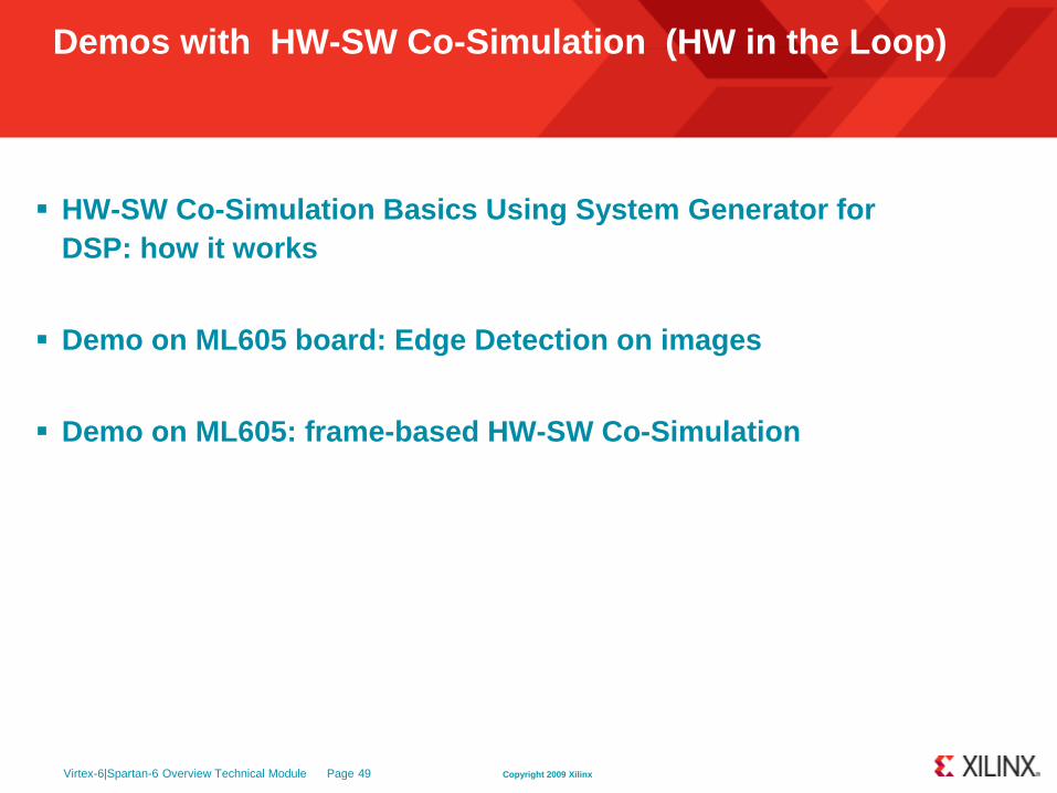
Demos with HW-SW Co-Simulation (HW in the Loop)
HW-SW Co-Simulation Basics Using System Generator for
DSP: how it works
Demo on ML605 board: Edge Detection on images
Demo on ML605: frame-based HW-SW Co-Simulation
Virtex-6|Spartan-6 Overview Technical Module Page 49
Copyright 2009 Xilinx
Demos with HW-SW Co-Simulation (HW in the Loop)
HW-SW Co-Simulation Basics Using System Generator for
DSP: how it works
Demo on ML605 board: Edge Detection on images
Demo on ML605: frame-based HW-SW Co-Simulation
Virtex-6|Spartan-6 Overview Technical Module Page 50
Slide 51
HW-SW Co-Simulation Basics Using System
Generator for DSP: how it works
Copyright 2009 XilinxPage 52
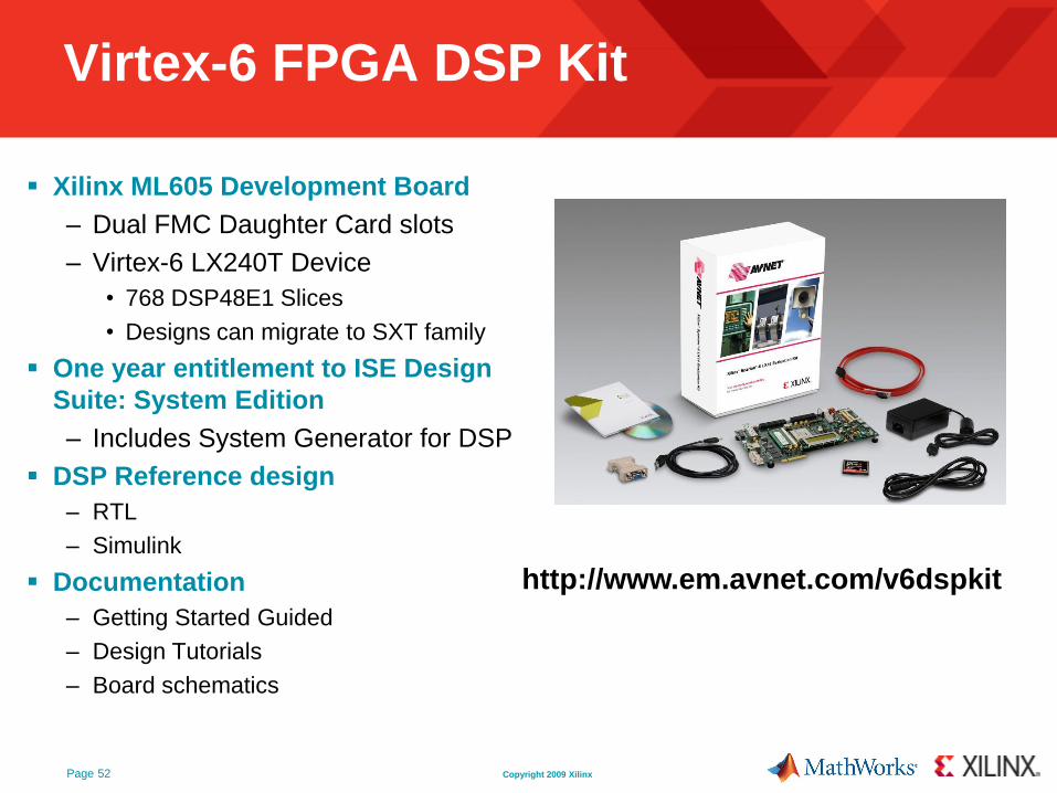
Virtex-6 FPGA DSP Kit
Xilinx ML605 Development Board
– Dual FMC Daughter Card slots
– Virtex-6 LX240T Device
• 768 DSP48E1 Slices
• Designs can migrate to SXT family
One year entitlement to ISE Design
Suite: System Edition
– Includes System Generator for DSP
DSP Reference design
– RTL
– Simulink
Documentation
– Getting Started Guided
– Design Tutorials
– Board schematics
http://www.em.avnet.com/v6dspkit
Copyright 2009 XilinxPage 53
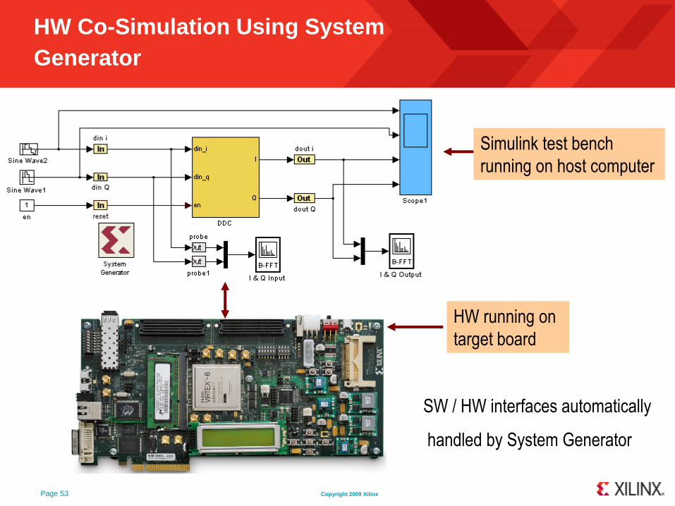
HW Co-Simulation Using System
Generator
Simulink test bench
running on host computer
HW running on
target board
SW / HW interfaces automatically
handled by System Generator
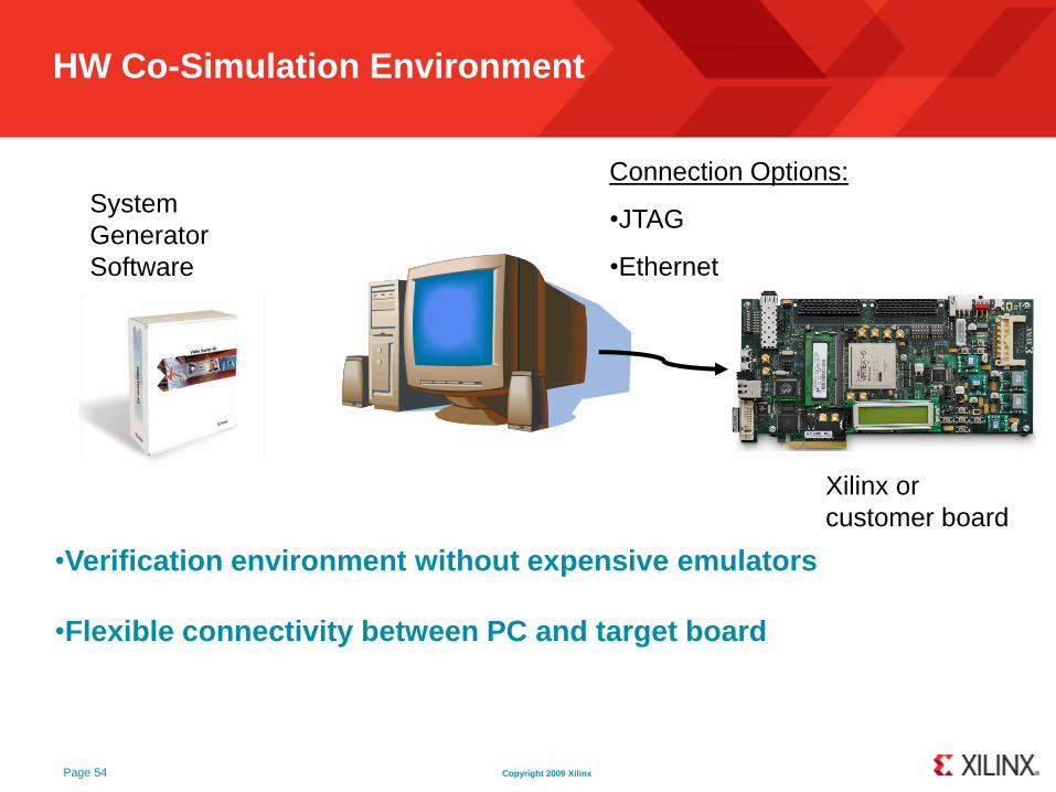
Copyright 2009 XilinxPage 54
HW Co-Simulation Environment
Connection Options:
•JTAG
•Ethernet
Xilinx or
customer board
System
Generator
Software
•Verification environment without expensive emulators
•Flexible connectivity between PC and target board
Copyright 2009 XilinxPage 55
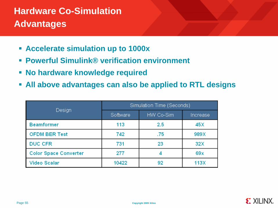
Hardware Co-Simulation
Advantages
Accelerate simulation up to 1000x
Powerful Simulink® verification environment
No hardware knowledge required
All above advantages can also be applied to RTL designs
Copyright 2009 XilinxPage 56
Basic Steps
Basic steps in the process
Build your design
Create a testbench
Choose your target HW
Compile & run
Copyright 2009 XilinxPage 57
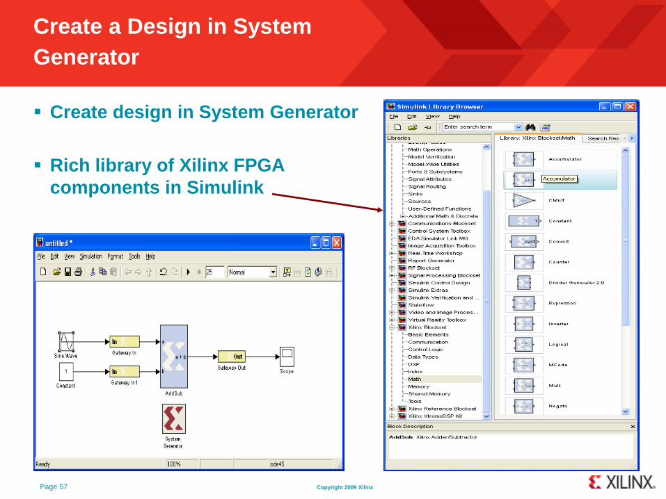
Create a Design in System
Generator
Create design in System Generator
Rich library of Xilinx FPGA
components in Simulink
Copyright 2009 XilinxPage 58
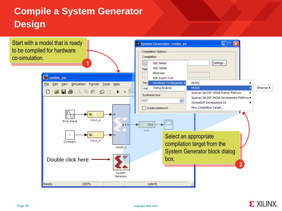
Compile a System Generator
Design
Select an appropriate
compilation target from the
System Generator block dialog
box.
Start with a model that is ready
to be compiled for hardware
co-simulation.1
2Double click here
Copyright 2009 XilinxPage 59
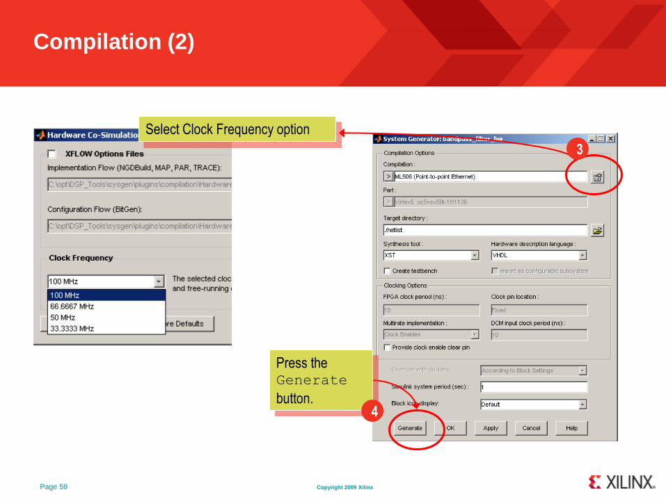
Compilation (2)
Press the Generate
button.
Select Clock Frequency option
3
4
Copyright 2009 XilinxPage 60
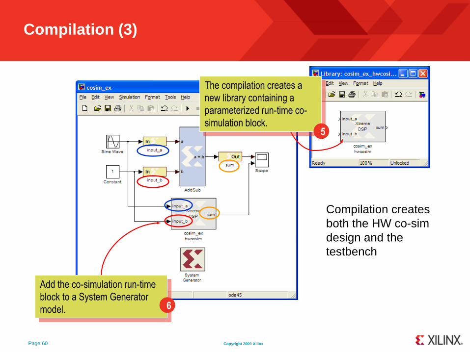
Compilation (3)
Add the co-simulation run-time
block to a System Generator
model.
The compilation creates a
new library containing a
parameterized run-time co-
simulation block.5
6
Compilation creates
both the HW co-sim
design and the
testbench
Copyright 2009 XilinxPage 61
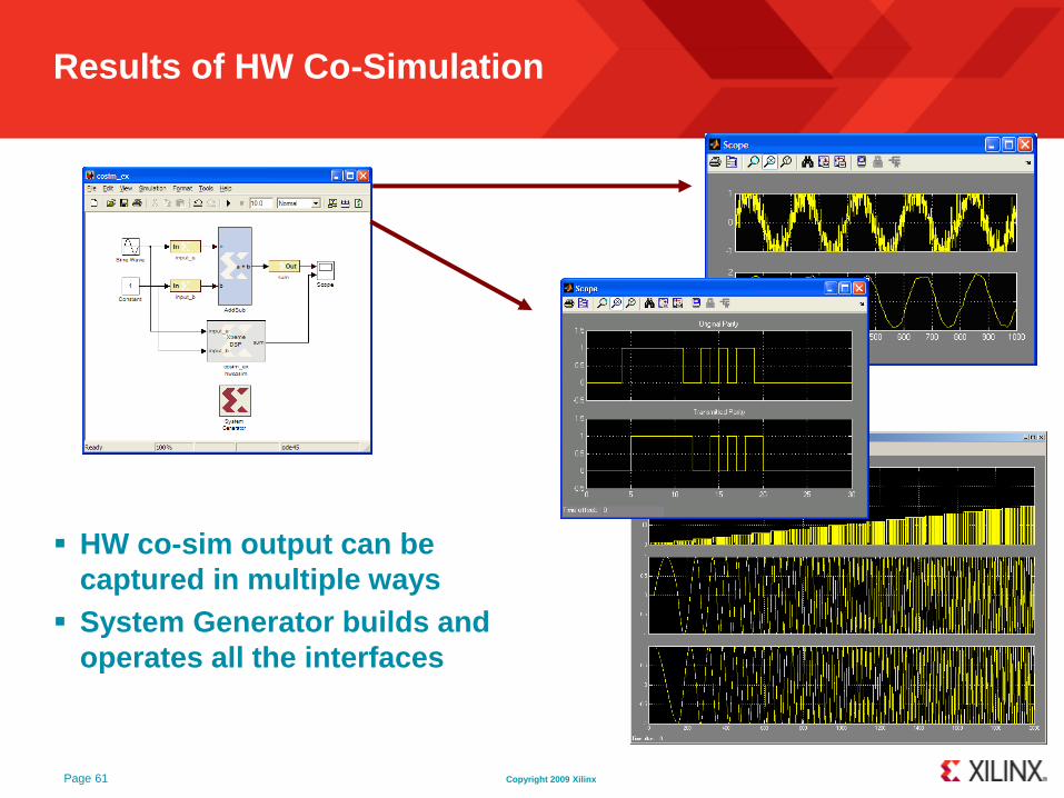
HW co-sim output can be
captured in multiple ways
System Generator builds and
operates all the interfaces
Results of HW Co-Simulation
Copyright 2009 XilinxPage 62
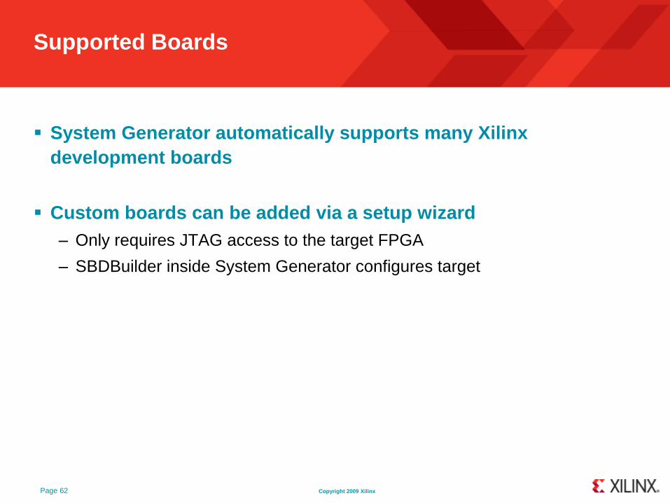
Supported Boards
System Generator automatically supports many Xilinx
development boards
Custom boards can be added via a setup wizard
– Only requires JTAG access to the target FPGA
– SBDBuilder inside System Generator configures target
Copyright 2009 XilinxPage 63
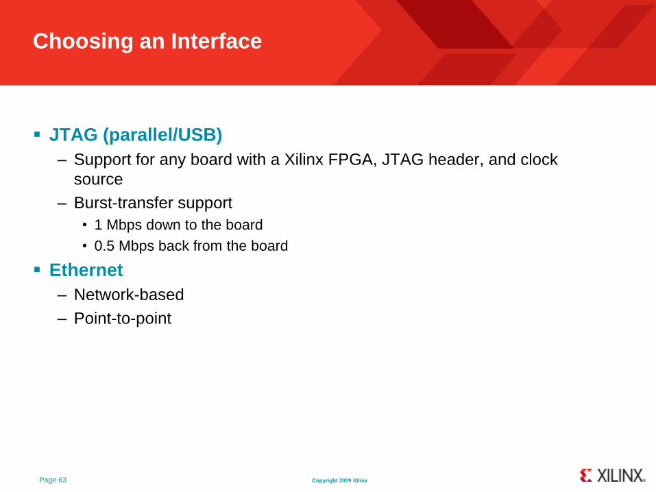
Choosing an Interface
JTAG (parallel/USB)
– Support for any board with a Xilinx FPGA, JTAG header, and clock
source
– Burst-transfer support
• 1 Mbps down to the board
• 0.5 Mbps back from the board
Ethernet
– Network-based
– Point-to-point
Copyright 2009 XilinxPage 64
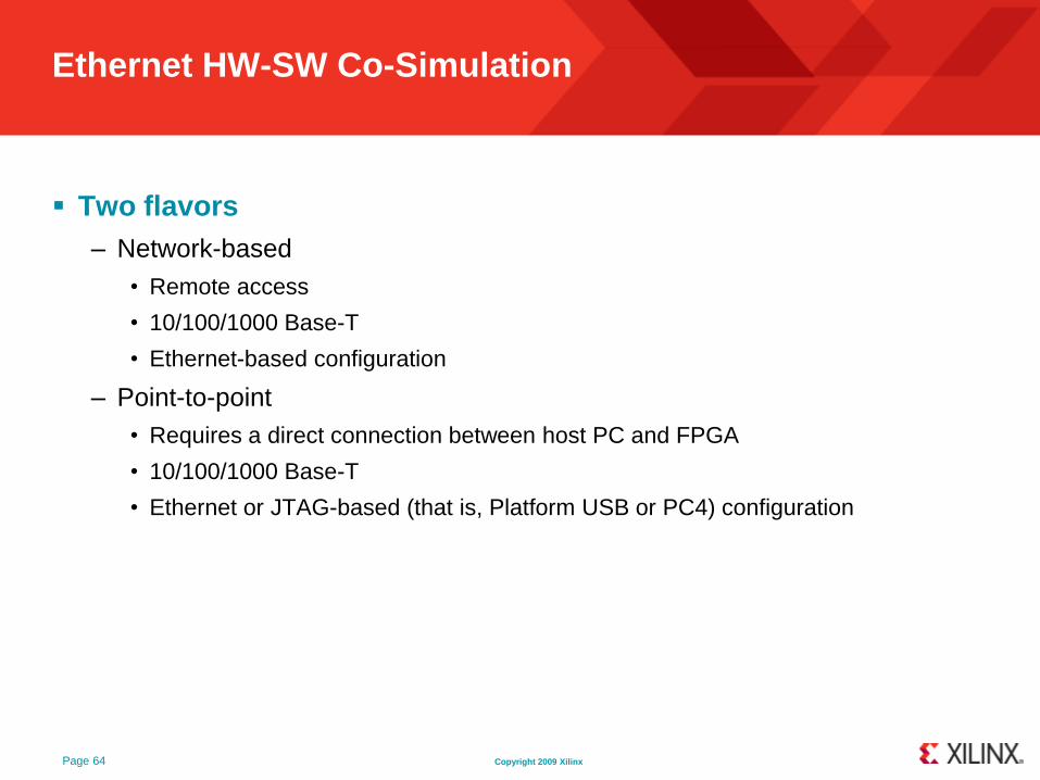
Ethernet HW-SW Co-Simulation
Two flavors
– Network-based
• Remote access
• 10/100/1000 Base-T
• Ethernet-based configuration
– Point-to-point
• Requires a direct connection between host PC and FPGA
• 10/100/1000 Base-T
• Ethernet or JTAG-based (that is, Platform USB or PC4) configuration
Copyright 2009 Xilinx
Demos with HW-SW Co-Simulation (HW in the Loop)
HW-SW Co-Simulation Basics Using System Generator for
DSP: how it works
Demo on ML605 board: Edge Detection on images
Demo on ML605: frame-based HW-SW Co-Simulation
Virtex-6|Spartan-6 Overview Technical Module Page 65
Demo on ML605 board:
Edge Detection on images
66
Copyright 2009 Xilinx
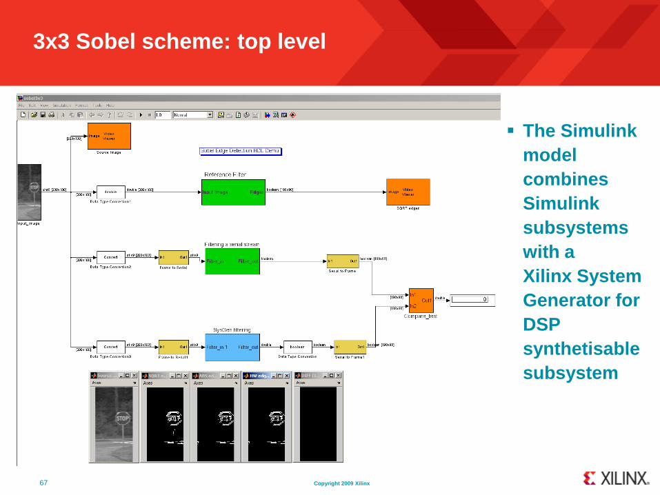
3x3 Sobel scheme: top level
The Simulink
model
combines
Simulink
subsystems
with a
Xilinx System
Generator for
DSP
synthetisable
subsystem
67
Copyright 2009 Xilinx
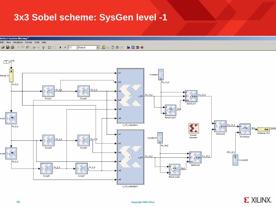
3x3 Sobel scheme: SysGen level -1
68
Copyright 2009 Xilinx
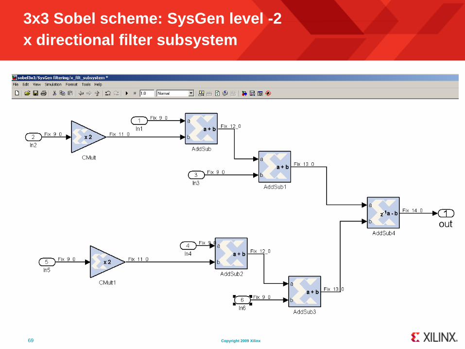
3x3 Sobel scheme: SysGen level -2
x directional filter subsystem
69
Copyright 2009 Xilinx
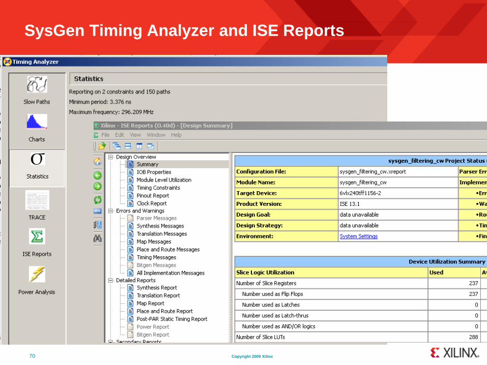
SysGen Timing Analyzer and ISE Reports
70
Copyright 2009 Xilinx
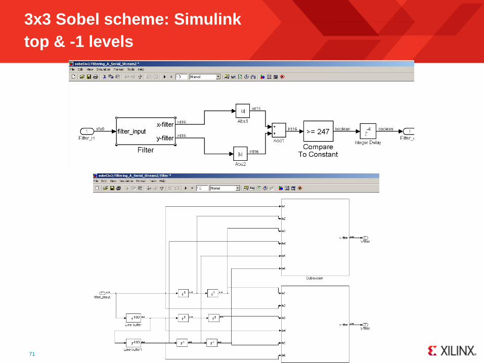
3x3 Sobel scheme: Simulink
top & -1 levels
71
Copyright 2009 Xilinx
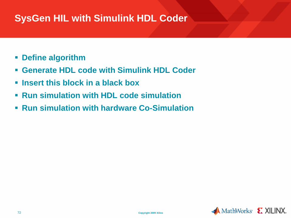
SysGen HIL with Simulink HDL Coder
Define algorithm
Generate HDL code with Simulink HDL Coder
Insert this block in a black box
Run simulation with HDL code simulation
Run simulation with hardware Co-Simulation
72
Copyright 2009 Xilinx
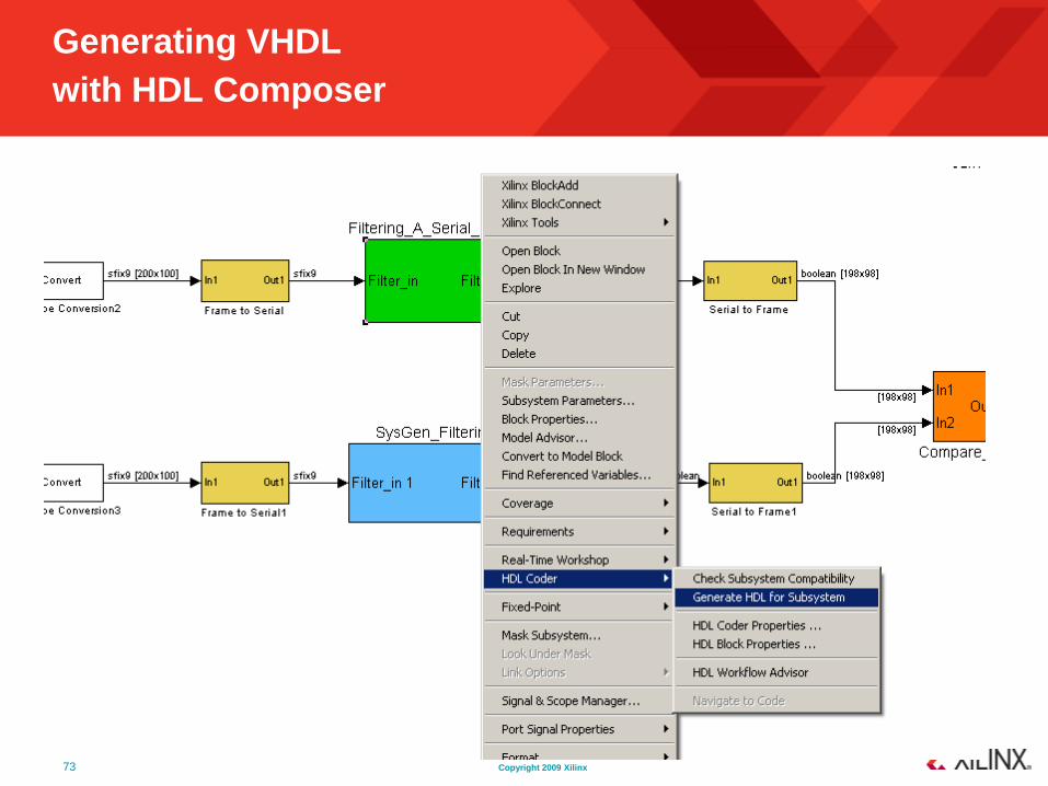
Generating VHDL
with HDL Composer
73
Copyright 2009 Xilinx
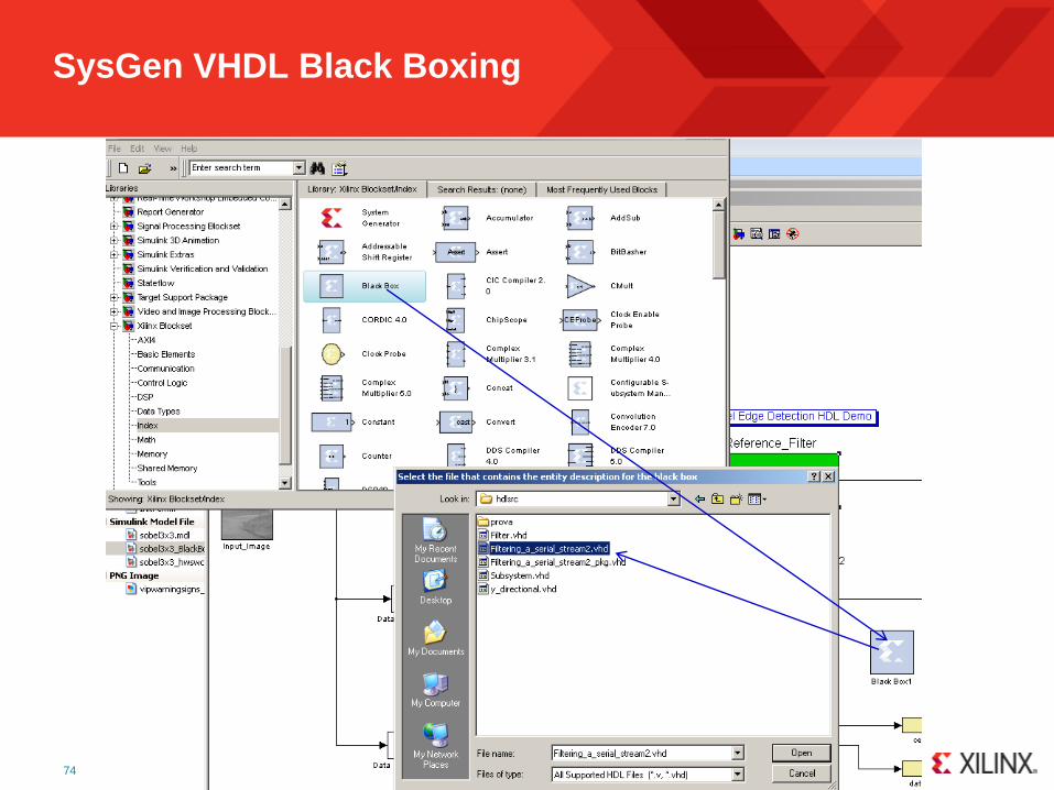
SysGen VHDL Black Boxing
74
Copyright 2009 Xilinx
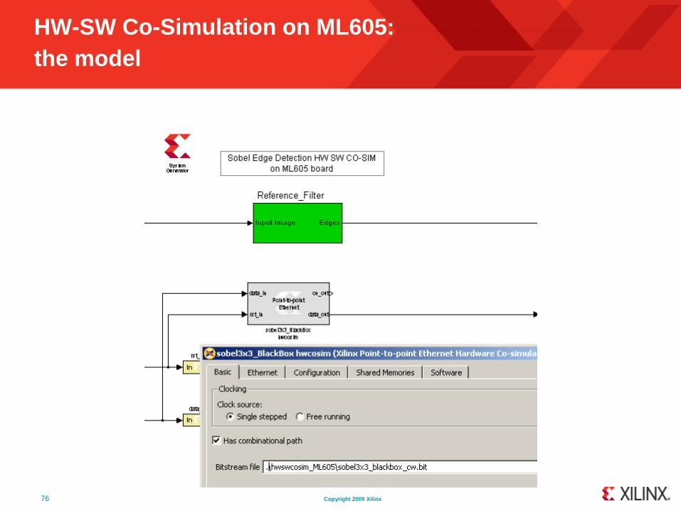
HW-SW Co-Simulation on ML605:
the model
76
Copyright 2009 Xilinx
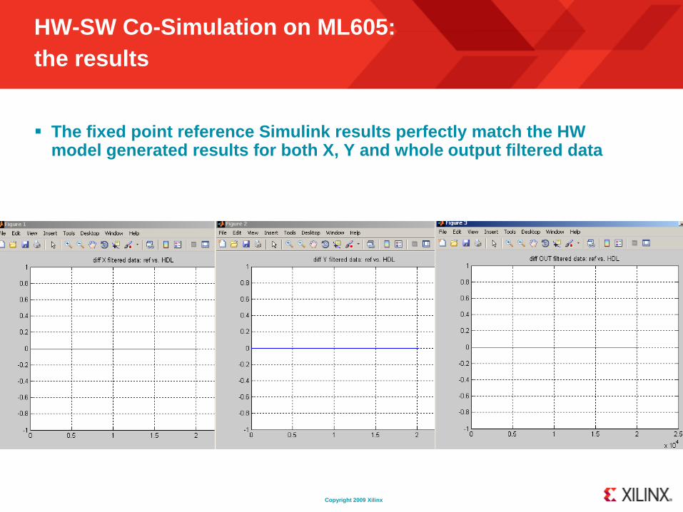
HW-SW Co-Simulation on ML605:
the results
The fixed point reference Simulink results perfectly match the HW model generated results for both X, Y and whole output filtered data
Copyright 2009 Xilinx
Demos with HW-SW Co-Simulation (HW in the Loop)
HW-SW Co-Simulation Basics Using System Generator for
DSP: how it works
Demo on ML605 board: Edge Detection on images
Demo on ML605: frame-based HW-SW Co-Simulation
Virtex-6|Spartan-6 Overview Technical Module Page 78
Slide 79
Demo on ML605:
frame-based HW-SW Co-Simulation
Copyright 2009 XilinxPage 80
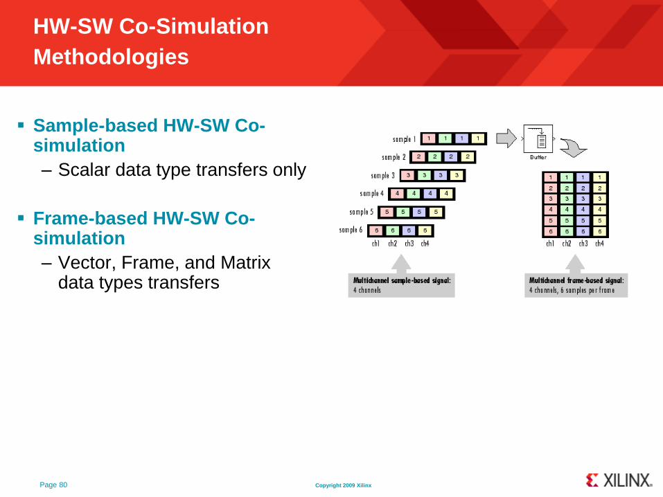
HW-SW Co-Simulation
Methodologies
Sample-based HW-SW Co-simulation
– Scalar data type transfers only
Frame-based HW-SW Co-simulation
– Vector, Frame, and Matrix data types transfers
Copyright 2009 XilinxPage 81
Frame-Based Acceleration
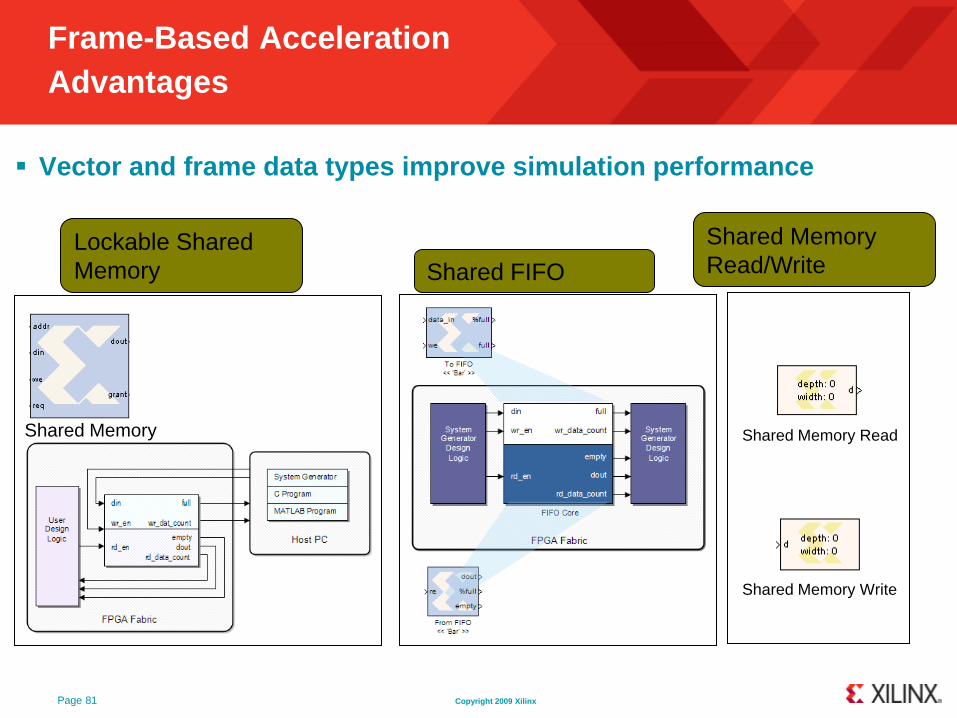
Advantages
Vector and frame data types improve simulation performance
Shared Memory Read
Shared Memory Write
Shared Memory
Lockable Shared
Memory Shared FIFO
Shared Memory
Read/Write
Copyright 2009 XilinxPage 82
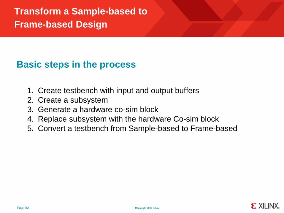
Transform a Sample-based to
Frame-based Design
Basic steps in the process
1. Create testbench with input and output buffers
2. Create a subsystem
3. Generate a hardware co-sim block
4. Replace subsystem with the hardware Co-sim block
5. Convert a testbench from Sample-based to Frame-based
Copyright 2009 XilinxPage 83
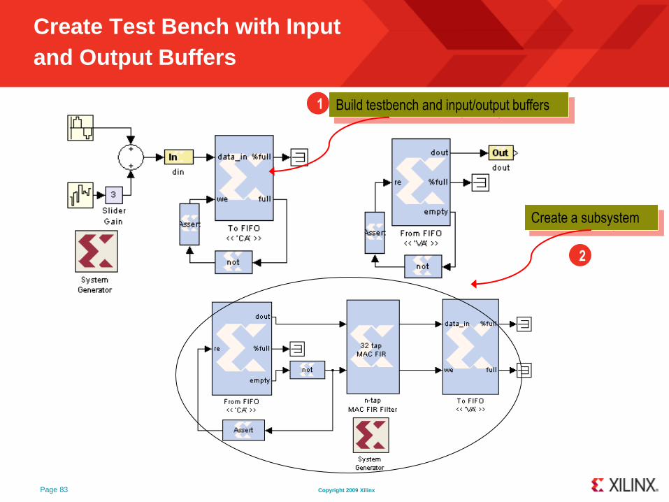
Create Test Bench with Input
and Output Buffers
Build testbench and input/output buffers1
Create a subsystem
2
Copyright 2009 XilinxPage 84
Generate HW Co-sim Block
Generate a hardware co-sim
block for the hardware_cosim
subsystem3
Replace hardware_cosim
subsystem with the hardware co-
sim block4
At Step.3: Software Simulink® simulation can
be performed at this point
At Step.4: hardware co-simulation can be
performed at this step but it’s still using single
word, data transfers (scalar data type)
Copyright 2009 XilinxPage 85
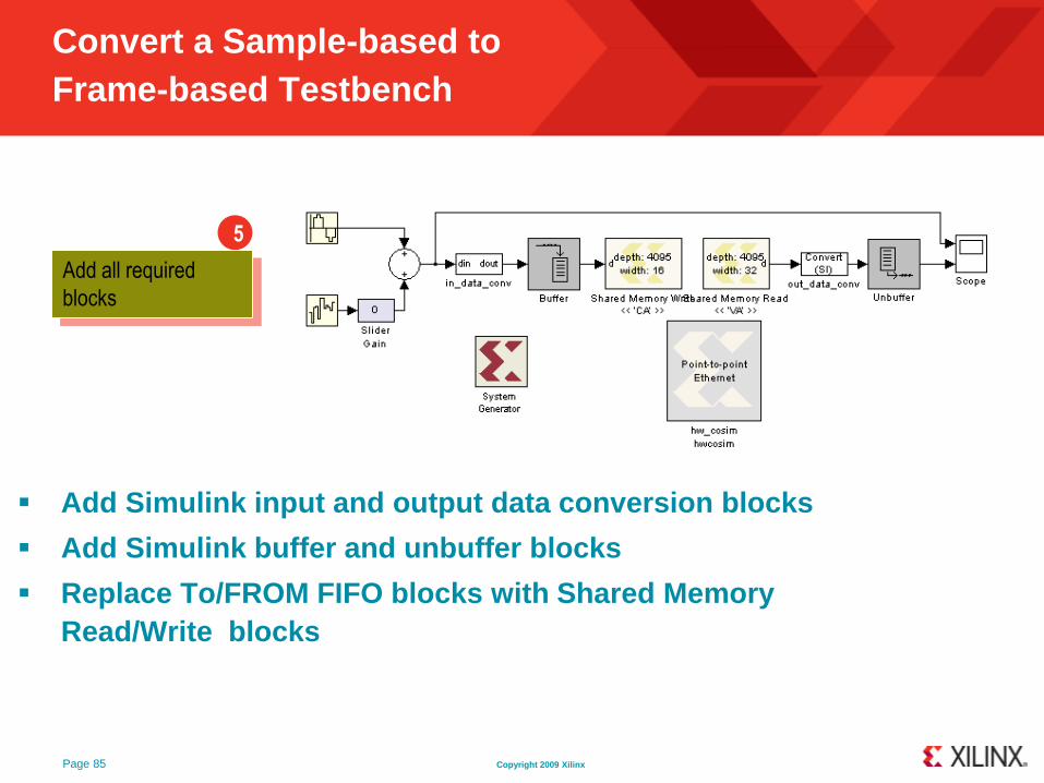
Convert a Sample-based to
Frame-based Testbench
5
Add Simulink input and output data conversion blocks
Add Simulink buffer and unbuffer blocks
Replace To/FROM FIFO blocks with Shared Memory
Read/Write blocks
Add all required
blocks
Copyright 2009 XilinxPage 86
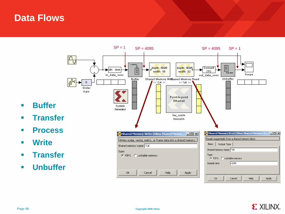
Data Flows
Buffer
Transfer
Process
Write
Transfer
Unbuffer
SP = 1 SP = 4095 SP = 4095 SP = 1
Copyright 2009 XilinxPage 87
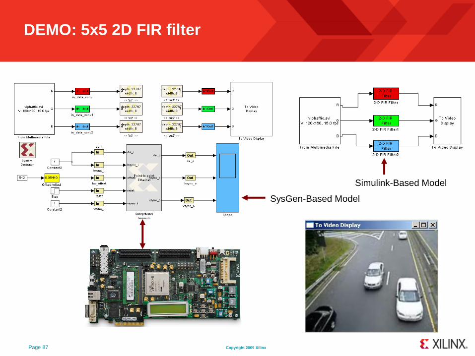
DEMO: 5x5 2D FIR filter
Simulink-Based Model
SysGen-Based Model
Copyright 2009 Xilinx
Outlines
Xilinx corporate
Virtex-6 / Spartan-6 family overview
7-series: a new family
Digital Signal Processing on FPGAs
System Generator for DSP overview
High Level Synthesis from C: AutoESL
Demos with HW-SW Co-Simulation (HW in the Loop)
Conclusion
94
Conclusion
Copyright 2009 Xilinx
Summary
XILINX Virtex-6, Spartan-6 and 7-series are optimized for
performance, low power consumption and ease of use
XILINX FPGAs are best choice for High performance DSP
– Up to 5280 DSP48
– Up to 3.4 TMACC in a single chip
System Generator for DSP is the XILINX reference tool for DSP
development
– Based on MALAB/Simulink
– HDL code insertion (Black Box)
– HW-SW CO-SIM with any FPGA board (JTAG)
AutoESL is the newest Xilinx tool for High Level Synthesis
directly from C/C++/SystemC
Page 96