Embed Size (px)
DESCRIPTION
ee
Citation preview
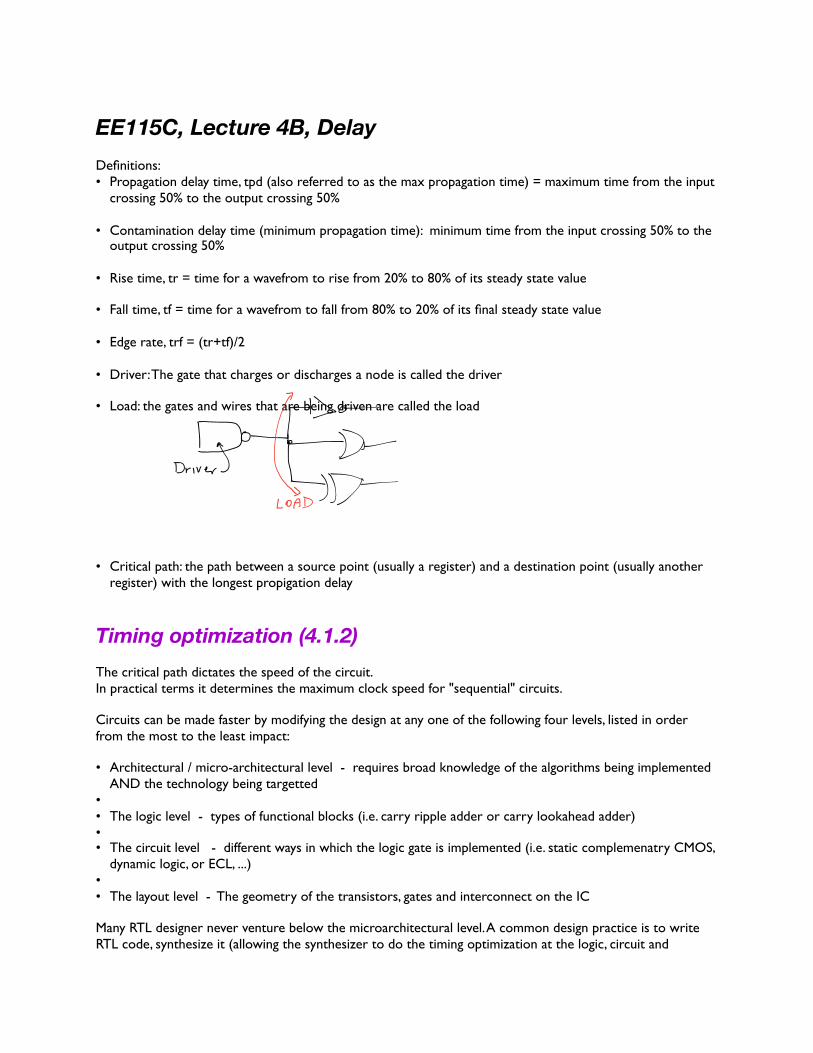
EE115C, Lecture 4B, DelayDefinitions:
Propagation delay time, tpd (also referred to as the max propagation time) = maximum time from the input •crossing 50% to the output crossing 50%
Contamination delay time (minimum propagation time): minimum time from the input crossing 50% to the •output crossing 50%
Rise time, tr = time for a wavefrom to rise from 20% to 80% of its steady state value•
Fall time, tf = time for a wavefrom to fall from 80% to 20% of its final steady state value•
Edge rate, trf = (tr+tf)/2•
Driver: The gate that charges or discharges a node is called the driver•
Load: the gates and wires that are being driven are called the load•
Critical path: the path between a source point (usually a register) and a destination point (usually another •register) with the longest propigation delay
Timing optimization (4.1.2) The critical path dictates the speed of the circuit. In practical terms it determines the maximum clock speed for "sequential" circuits.
Circuits can be made faster by modifying the design at any one of the following four levels, listed in order from the most to the least impact:
Architectural / micro-architectural level - requires broad knowledge of the algorithms being implemented •AND the technology being targetted
•The logic level - types of functional blocks (i.e. carry ripple adder or carry lookahead adder)•
•The circuit level - different ways in which the logic gate is implemented (i.e. static complemenatry CMOS, •dynamic logic, or ECL, ...)
•The layout level - The geometry of the transistors, gates and interconnect on the IC•
Many RTL designer never venture below the microarchitectural level. A common design practice is to write RTL code, synthesize it (allowing the synthesizer to do the timing optimization at the logic, circuit and
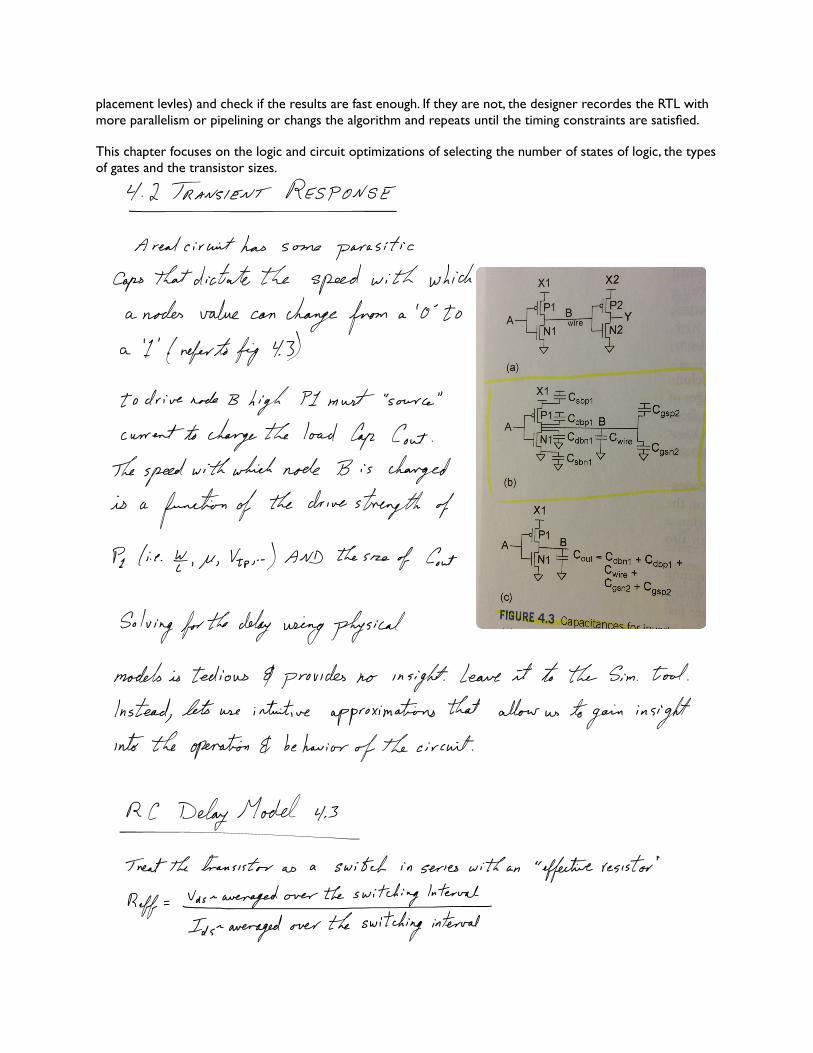
placement levles) and check if the results are fast enough. If they are not, the designer recordes the RTL with more parallelism or pipelining or changs the algorithm and repeats until the timing constraints are satisfied.
This chapter focuses on the logic and circuit optimizations of selecting the number of states of logic, the types of gates and the transistor sizes.
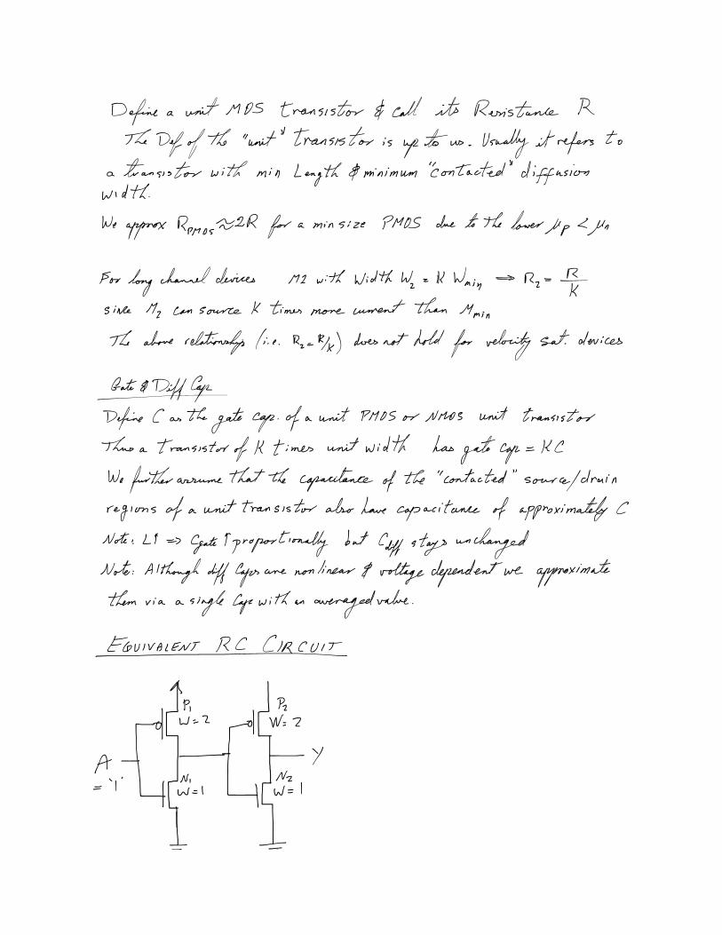
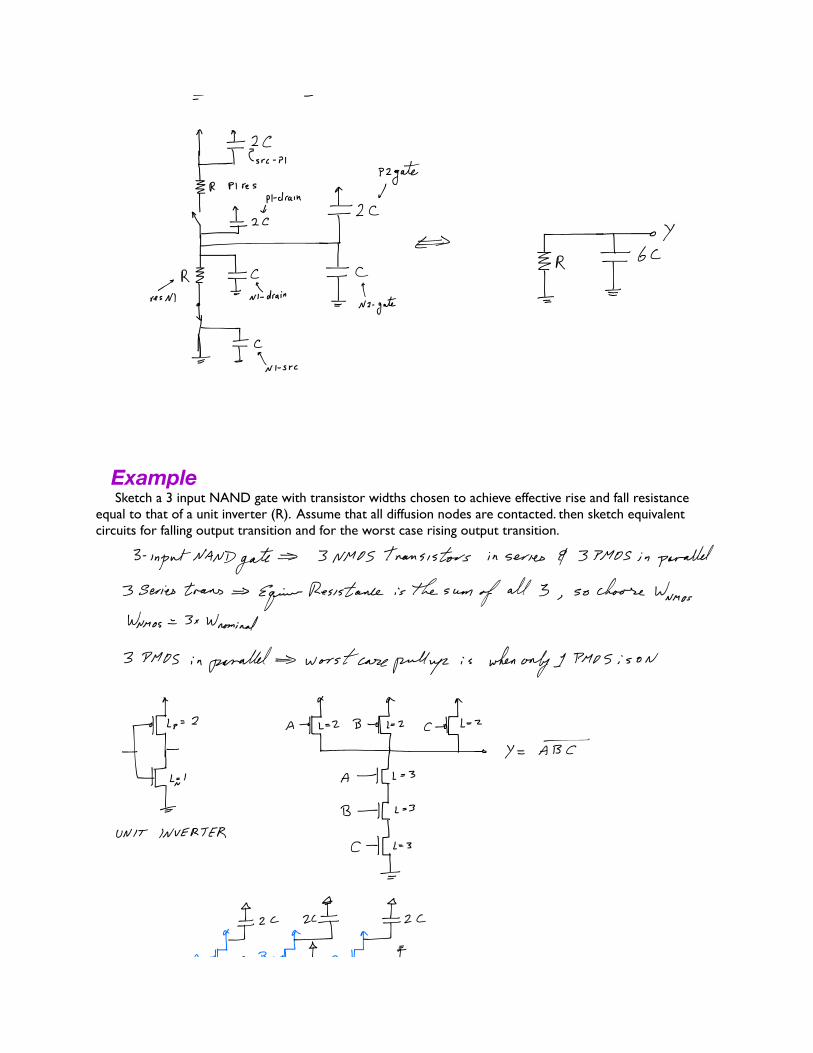
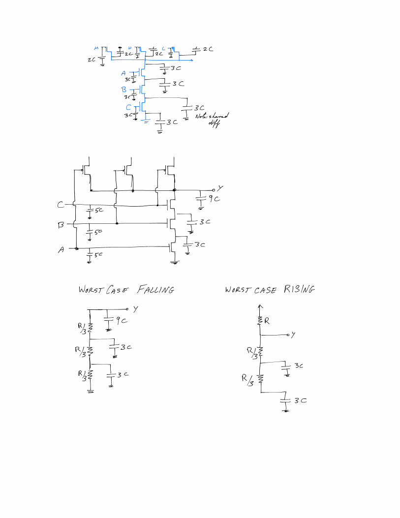
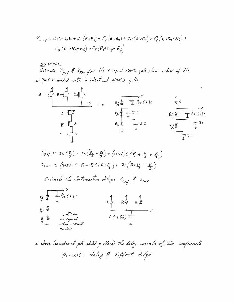
Example Sketch a 3 input NAND gate with transistor widths chosen to achieve effective rise and fall resistance equal to that of a unit inverter (R). Assume that all diffusion nodes are contacted. then sketch equivalent circuits for falling output transition and for the worst case rising output transition.