Embed Size (px)
Citation preview
1
EE 215A Fundamentals of Electrical Engineering Lecture Notes
Operational Amplifiers (Op Amps) 8/6/01 Reviewed 10/04
Rich Christie
Overview: The operational amplifier, or op amp for short, is a fundamental building block in circuit design. Stuffed inside a chip are a bunch of transistors and other elements that make up a near-ideal voltage controlled voltage source (VCVS) with near-infinite gain. We'll start by assuming it is ideal. Circuit Symbol: The op amp has a special circuit symbol, a triangle with two inputs and one output
The + and - connections are the non-inverting input and the inverting input. These are usually, but not always, drawn with the minus (-) at the top. Ideal Op Amps Relationships: An ideal op amp is an ideal voltage controlled voltage source. We can think of the op amp symbol being replaced as follows:
+
-v1
v2
vo
i1
i2
io+
-
v2
v1
vo
i2
i1
io
+
-v1
v2
vo
i1
i2
io
+
-
vo = !( v2- v1)
+
- v1
v2
vo
i1
i2
io
2
Notice what this implies: If vo is finite, then
012
=!
=" ov
vv
21vv =
and
0
0
2
1
=
=
i
i
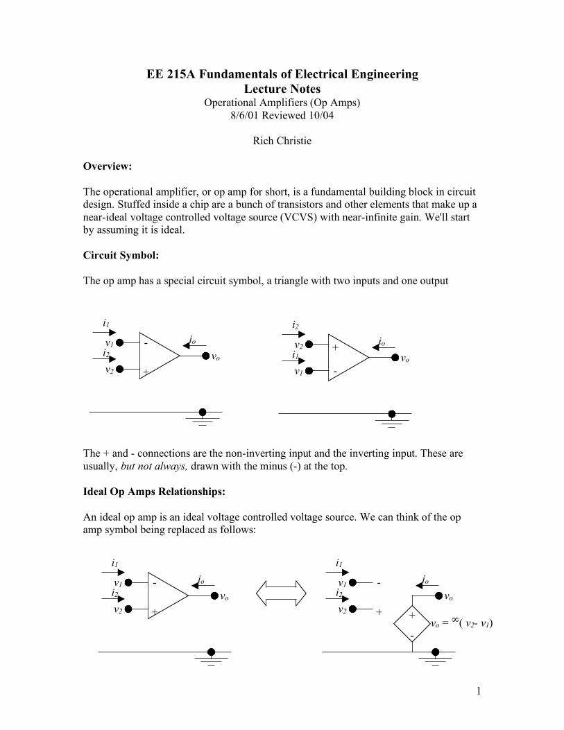
These are in fact the ideal op amp relationships, and once we get used to them we can use them to solve op amp circuits. (At this point you might be wondering why the op amp has its own special symbol when it's really just a VCVS. The answer has to do with packaging. The op amp comes in a single package which includes the inverting and non-inverting inputs. The op amp symbol indicates that the package combines all the connections in one place, where the VCVS symbol lets the inputs be anywhere.) Op Amp Power Supplies: But wait, if the input currents i1 and i2 are zero, where does the output current io come from? The dependent voltage source, in the model, but in real life, we have to supply the op amp with an external power supply. Many real world op amps (the LM741, for example) require both positive and negative voltage (as opposed to positive and ground, called single source.) If you really want to do KCL for the op amp (for a supernode containing the op amp, or for the output node), you have to include the power supply. Usually it's not necessary and the power supply connections are omitted - we all understand that they are there, so why clutter up the circuit with them?
+
-v1
v2
vo
i1
i2
io
v+
v-
3
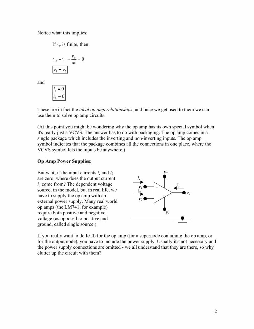
Op Amp Circuit Analysis: Let's try a circuit with an op amp. What's the relationship between vs and vo?
1vv
o= since they are connected.
ovvv ==
12 from the ideal op
amp relationships. Since 0
2=i ,
svv =
2 and thus
sovv =
This circuit is called a voltage follower or a buffer amplifier. At first glance we have not done much. But let's ask: consider the source (connected to v2) before it is connected to the op amp. What's the Thevenin equivalent resistance? It's pretty obvious that
stRR =
Now consider the Thevenin equivalent resistance seen looking in to the whole thing. voc is just vo, and isc is - well, it's infinite! (v2 must be vs because i2 is zero, then v1 must equal v2 which means vo is vs no matter what the current is but it is shorted -> infinite current.)
So 0==sc
oc
t
i
vR and the
Thevenin equivalent is an ideal voltage source of value vs:
+
- v1
v2 vo
io
+
-
vs
Rs
RL
i2
+
- v1
v2 vo
io
+
-
vs
Rs
RL
i2
+
-
vs
Rs
+
-
vs
4
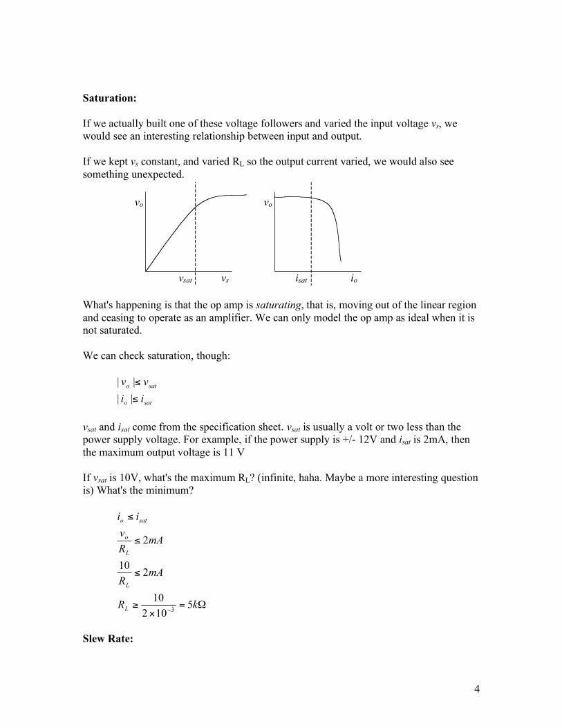
Saturation: If we actually built one of these voltage followers and varied the input voltage vs, we would see an interesting relationship between input and output. If we kept vs constant, and varied RL so the output current varied, we would also see something unexpected.
What's happening is that the op amp is saturating, that is, moving out of the linear region and ceasing to operate as an amplifier. We can only model the op amp as ideal when it is not saturated. We can check saturation, though:
sato
sato
ii
vv
!
!
||
||
vsat and isat come from the specification sheet. vsat is usually a volt or two less than the power supply voltage. For example, if the power supply is +/- 12V and isat is 2mA, then the maximum output voltage is 11 V If vsat is 10V, what's the maximum RL? (infinite, haha. Maybe a more interesting question is) What's the minimum?
!="
#
$
$
$
%kR
mAR
mAR
v
ii
L
L
L
o
sato
5102
10
210
2
3
Slew Rate:
vs
vo
io
vo
isatvsat
5
At this point we should probably note that another departure from ideality in the op amp
is that the slew rate, dt
dvo , is also limited. This affects how fast the op amp responds to a
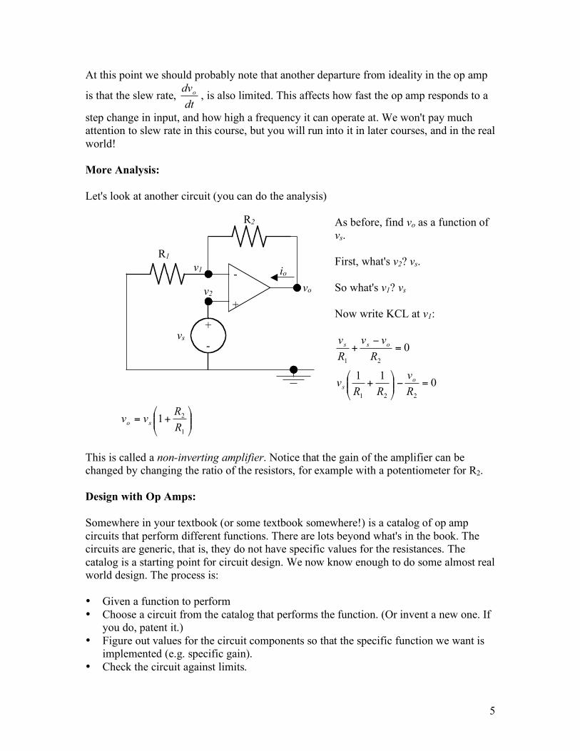
step change in input, and how high a frequency it can operate at. We won't pay much attention to slew rate in this course, but you will run into it in later courses, and in the real world! More Analysis: Let's look at another circuit (you can do the analysis)
As before, find vo as a function of vs. First, what's v2? vs. So what's v1? vs Now write KCL at v1:
0
21
=!
+R
vv
R
voss
011
221
=!""#
$%%&
'+
R
v
RRv
o
s
!!"
#$$%
&+=
1
21R
Rvvso
This is called a non-inverting amplifier. Notice that the gain of the amplifier can be changed by changing the ratio of the resistors, for example with a potentiometer for R2. Design with Op Amps: Somewhere in your textbook (or some textbook somewhere!) is a catalog of op amp circuits that perform different functions. There are lots beyond what's in the book. The circuits are generic, that is, they do not have specific values for the resistances. The catalog is a starting point for circuit design. We now know enough to do some almost real world design. The process is: • Given a function to perform • Choose a circuit from the catalog that performs the function. (Or invent a new one. If
you do, patent it.) • Figure out values for the circuit components so that the specific function we want is
implemented (e.g. specific gain). • Check the circuit against limits.
+
- v1
v2 vo
io
+
-
vs
R1
R2
6
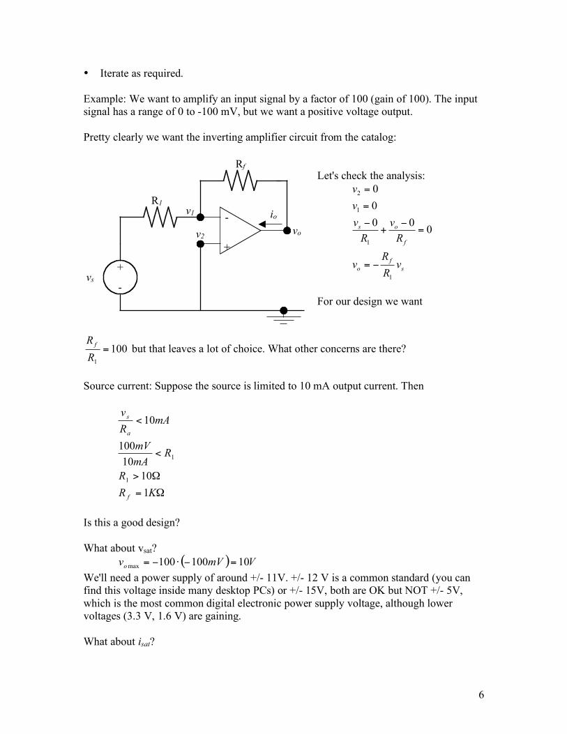
• Iterate as required. Example: We want to amplify an input signal by a factor of 100 (gain of 100). The input signal has a range of 0 to -100 mV, but we want a positive voltage output. Pretty clearly we want the inverting amplifier circuit from the catalog:
Let's check the analysis:
s
f
o
f
os
vR
Rv
R
v
R
v
v
v
1
1
1
2
000
0
0
!=
=!
+!
=
=
For our design we want
100
1
=R
R f but that leaves a lot of choice. What other concerns are there?
Source current: Suppose the source is limited to 10 mA output current. Then
!=
!>
<
<
KR
R
RmA
mV
mAR
v
f
a
s
1
10
10
100
10
1
1
Is this a good design? What about vsat? ( ) VmVv
o10100100
max=!"!=
We'll need a power supply of around +/- 11V. +/- 12 V is a common standard (you can find this voltage inside many desktop PCs) or +/- 15V, both are OK but NOT +/- 5V, which is the most common digital electronic power supply voltage, although lower voltages (3.3 V, 1.6 V) are gaining. What about isat?
+
- v1
v2 vo
io
+
-
vs
R1
Rf
7
)(!101
10mA
KR
vi
f
oo ===
Whoops, the limit we talked about earlier was 2 mA. (This limit will vary from op amp type to op amp type, so maybe we just need to buy a different op amp. But let's use the one in the parts kit… with a 2mA output current limit.) If we increase Rf, and increase R1 to keep the 100 ratio, then is will also go down, and we will meet both constraints.
!==
!=>
<
<
50100
52
10
2
2
1
RfR
kmA
R
mAR
v
mAi
f
f
o
o
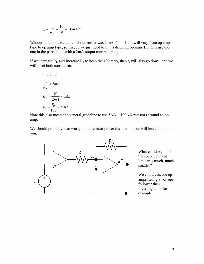
Note this also meets the general guideline to use 5 kΩ – 100 kΩ resistors around an op amp. We should probably also worry about resistor power dissipation, but will leave that up to you.
What could we do if the source current limit was much, much smaller? We could cascade op amps, using a voltage follower then inverting amp, for example.
+
- v1
v2 vo
io
+
-
vs
R1
Rf
+
-
8
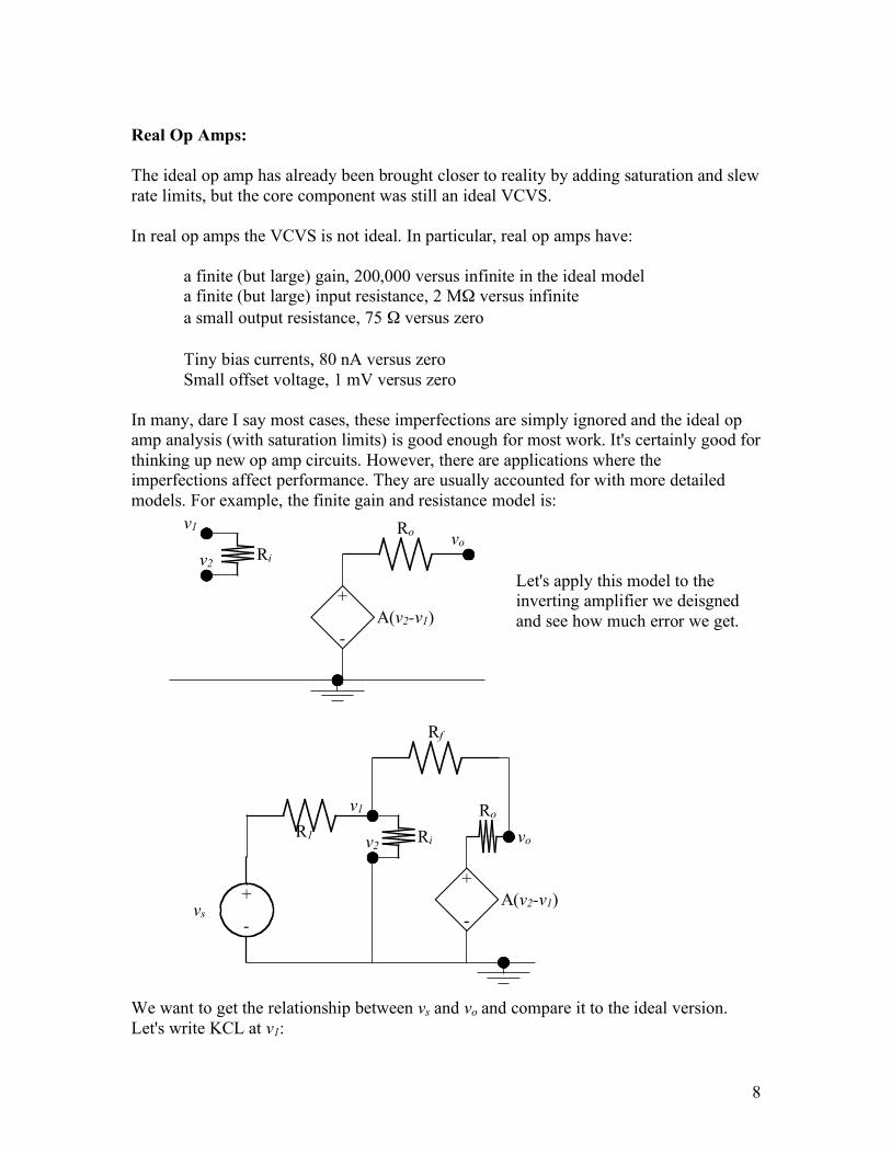
Real Op Amps: The ideal op amp has already been brought closer to reality by adding saturation and slew rate limits, but the core component was still an ideal VCVS. In real op amps the VCVS is not ideal. In particular, real op amps have:
a finite (but large) gain, 200,000 versus infinite in the ideal model a finite (but large) input resistance, 2 MΩ versus infinite a small output resistance, 75 Ω versus zero Tiny bias currents, 80 nA versus zero Small offset voltage, 1 mV versus zero
In many, dare I say most cases, these imperfections are simply ignored and the ideal op amp analysis (with saturation limits) is good enough for most work. It's certainly good for thinking up new op amp circuits. However, there are applications where the imperfections affect performance. They are usually accounted for with more detailed models. For example, the finite gain and resistance model is:
Let's apply this model to the inverting amplifier we deisgned and see how much error we get.
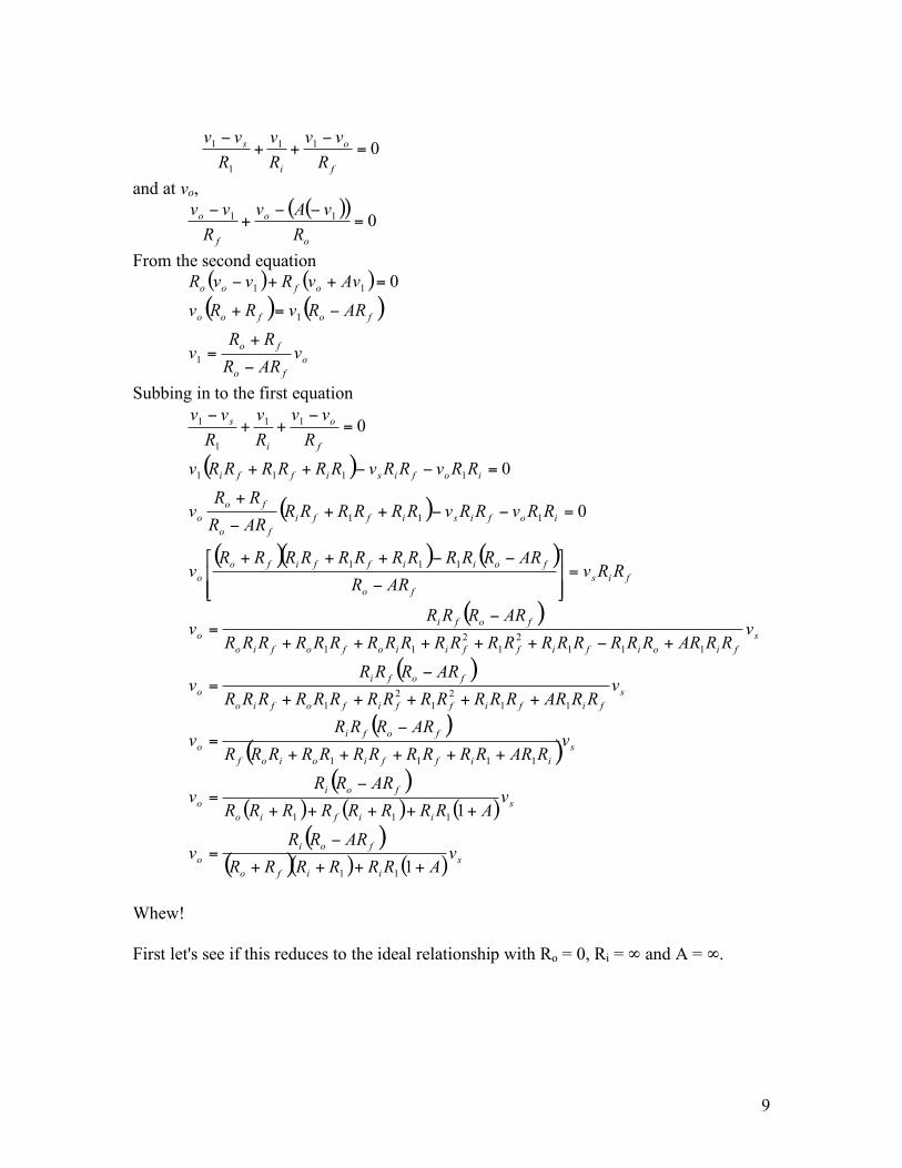
We want to get the relationship between vs and vo and compare it to the ideal version. Let's write KCL at v1:
v1
v2
vo
A(v2-v1)
Ri
Ro
+
-
v1
v2 vo
+
-vs
R1
Rf
A(v2-v1)
+
-
Ri
Ro
9
011
1
1 =!
++!
f
o
i
s
R
vv
R
v
R
vv
and at vo,
( )( )0
11 =!!
+!
o
o
f
o
R
vAv
R
vv
From the second equation
( ) ( )
( ) ( )
o
fo
fo
fofoo
ofoo
vARR
RRv
ARRvRRv
AvvRvvR
!
+=
!=+
=++!
1
1
110
Subbing in to the first equation
( )
( )
( )( ) ( )
( )
( )s
fififfifofio
fofi
o
s
fioififfiiofofio
fofi
o
fis
fo
foiiffifo
o
iofisiffi
fo
fo
o
iofisiffi
f
o
i
s
vRRARRRRRRRRRRRRRR
ARRRRv
vRRARRRRRRRRRRRRRRRRRRRR
ARRRRv
RRvARR
ARRRRRRRRRRRRv
RRvRRvRRRRRRARR
RRv
RRvRRvRRRRRRv
R
vv
R
v
R
vv
11
2
1
2
1
111
2
1
2
11
111
111
1111
11
1
1
0
0
0
+++++
!=
+!+++++
!=
=""#
$
%%&
'
!
!!+++
=!!++!
+
=!!++
=!
++!
( )( )
( )( ) ( ) ( )
( )( )( ) ( ) s
iifo
foi
o
s
iifio
foi
o
s
iiffioiof
fofi
o
vARRRRRR
ARRRv
vARRRRRRRR
ARRRv
vRARRRRRRRRRRRR
ARRRRv
++++
!=
+++++
!=
+++++
!=
1
1
11
111
1111
Whew!
First let's see if this reduces to the ideal relationship with Ro = 0, Ri = ∞ and A = ∞.
10
( ) ( )
( )( )
s
f
sf
f
o
s
f
f
s
i
f
i
if
f
o
s
iif
fi
o
vR
Rv
A
AR
A
R
A
R
Rv
vARR
ARv
ARR
RR
R
RR
ARv
vARRRRR
RARv
1
1
1
1
1
1
11
11
1
!=
++
!=
++
!=
+++
!=
+++
!=
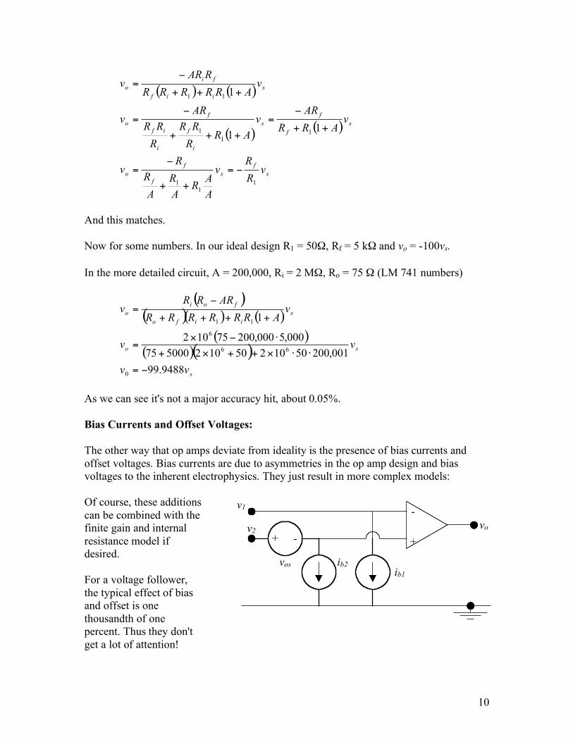
And this matches. Now for some numbers. In our ideal design R1 = 50Ω, Rf = 5 kΩ and vo = -100vs. In the more detailed circuit, A = 200,000, Ri = 2 MΩ, Ro = 75 Ω (LM 741 numbers)
( )( )( ) ( )
( )( )( )
s
so
s
iifo
foi
o
vv
vv
vARRRRRR
ARRRv
9488.99
001,2005010250102500075
000,5000,20075102
1
0
66
6
11
!=
""#++#+
"!#=
++++
!=
As we can see it's not a major accuracy hit, about 0.05%. Bias Currents and Offset Voltages:
The other way that op amps deviate from ideality is the presence of bias currents and offset voltages. Bias currents are due to asymmetries in the op amp design and bias voltages to the inherent electrophysics. They just result in more complex models: Of course, these additions can be combined with the finite gain and internal resistance model if desired. For a voltage follower, the typical effect of bias and offset is one thousandth of one percent. Thus they don't get a lot of attention!
+
-v1
v2vo
+ -
ib1
ib2vos
11
Common Mode Gain: Even in the finite gain model of the op amp, the gain is considered constant. In fact, it depends on the average of the input voltages and also on the frequency of the input. The dependence on average is called common mode gain. The VCVS voltage equation is really
( ) !"
#$%
& ++'
2
21
12
vvAvvAcm
The common mode gain Acm is hidden in the specs as the common mode rejection ratio (CMRR). (No engineer social life jokes, please).
A
ACMRR
cm=
With CMRRs of 31,600 (as the LOW value) this can often be ignored. Variation of gain with frequency is similarly disguised in the specs as gain-bandwidth product. What really stays constant is gain times frequency (dc and near-dc is a special case!)
( )
( )f
BfA
ffAB
=
!=
And that's pretty much it for op amps until we know something about energy storage devices.


![11 March 2011: Japan Earthquake and Pacific Tsunami ... are typically placed on an ICS-215A form (Incident Action Plan Safety and Risk Analysis Form) [See Appendix B]; typical to the](https://img.pdfslide.net/doc/110x75/5aea75597f8b9a66258c0ff5/11-march-2011-japan-earthquake-and-pacific-tsunami-are-typically-placed-on.jpg)