Embed Size (px)
Citation preview
EECS 247 Lecture 18: Data Converters- Track & Hold- ADC Design © 2010 Page 1
EE247
Lecture 18ADC Converters
– Track & hold • T/H circuits
• T/H combined with summing/difference function
• T/H circuit incorporating gain & offset cancellation
• T/H aperture uncertainty
– ADC architectures and design • Serial- slope type
• Successive approximation
• Flash ADC and its sources of error: comparator offset, sparkle code & meta-stability
– Comparator design • Single-stage open-loop amplifier
• Cascade of open-loop amplifiers
EECS 247 Lecture 17: Data Converters- ADC Design, Sampling © 2010 Page 2
Summary of Last Lecture
ADC Converters
– Sampling (continued)• Sampling switch considerations
– Clock voltage boosters
• Sampling switch charge injection & clock feedthrough
– Complementary switch
– Use of dummy device
– Bottom-plate switching
– Track & hold • Flip around T/H
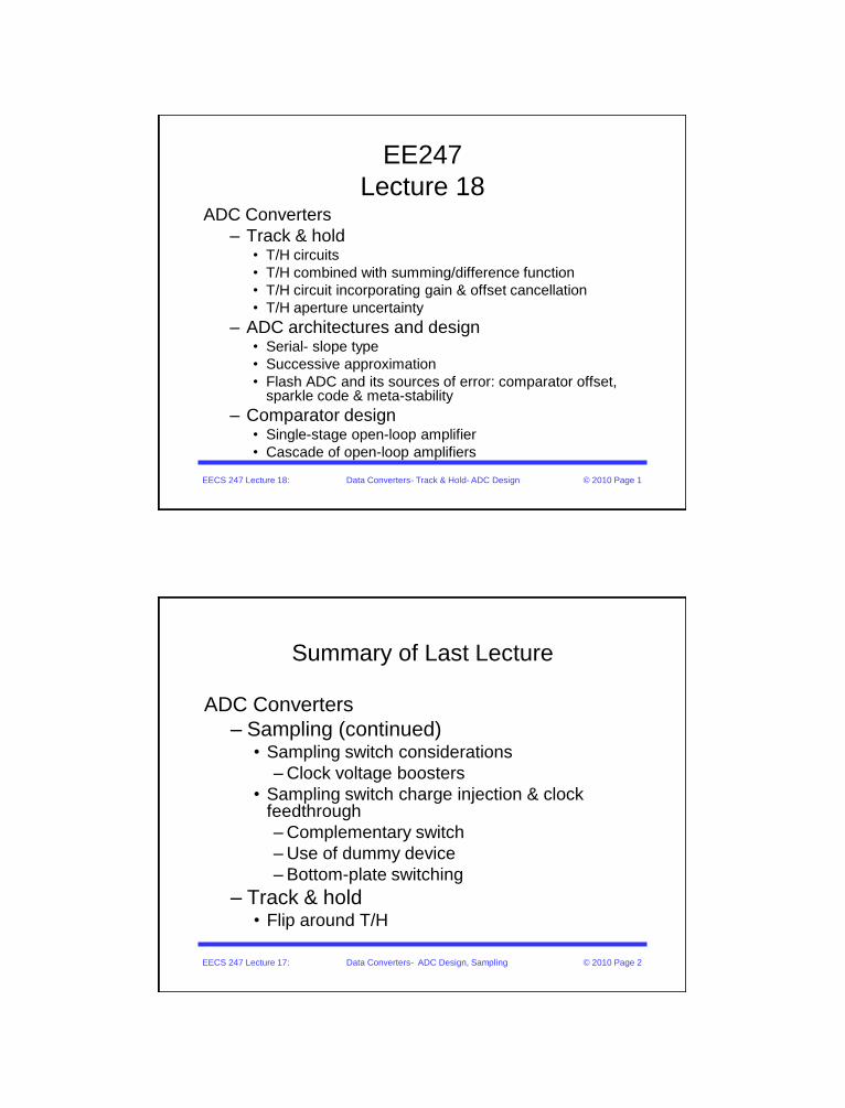
EECS 247 Lecture 17: Data Converters- Track & Hold- ADC Design © 2009 Page 3
Flip-Around T/H-Basic Operation
f1high
vIN vOUT
C
S1A
f1D
S2
f2
S2A
f2
S3
f1D
f1 S1
vCM
Charging C
f1
f1D
f2
Note: Opamp has to be
stable in unity-gain
configuration
Qf1=VINxC
EECS 247 Lecture 17: Data Converters- Track & Hold- ADC Design © 2009 Page 4
Flip-Around T/H-Basic Operation
f2high
vINvOUT
C
S1A
f1D
S2
f2
S2A
f2
S3
f1D
f1 S1
vCM
Holding
f1
f2
f1D
Qf2=VOUT xC
VOUT = VIN
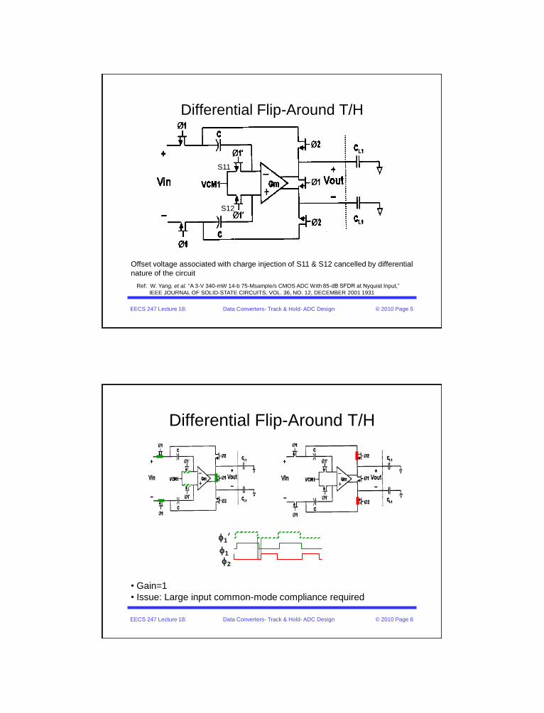
EECS 247 Lecture 18: Data Converters- Track & Hold- ADC Design © 2010 Page 5
Differential Flip-Around T/H
Ref: W. Yang, et al. “A 3-V 340-mW 14-b 75-Msample/s CMOS ADC With 85-dB SFDR at Nyquist Input,”
IEEE JOURNAL OF SOLID-STATE CIRCUITS, VOL. 36, NO. 12, DECEMBER 2001 1931
Offset voltage associated with charge injection of S11 & S12 cancelled by differential
nature of the circuit
S11
S12
EECS 247 Lecture 18: Data Converters- Track & Hold- ADC Design © 2010 Page 6
Differential Flip-Around T/H
• Gain=1
• Issue: Large input common-mode compliance required
f1’
f1
f2
EECS 247 Lecture 18: Data Converters- Track & Hold- ADC Design © 2010 Page 7
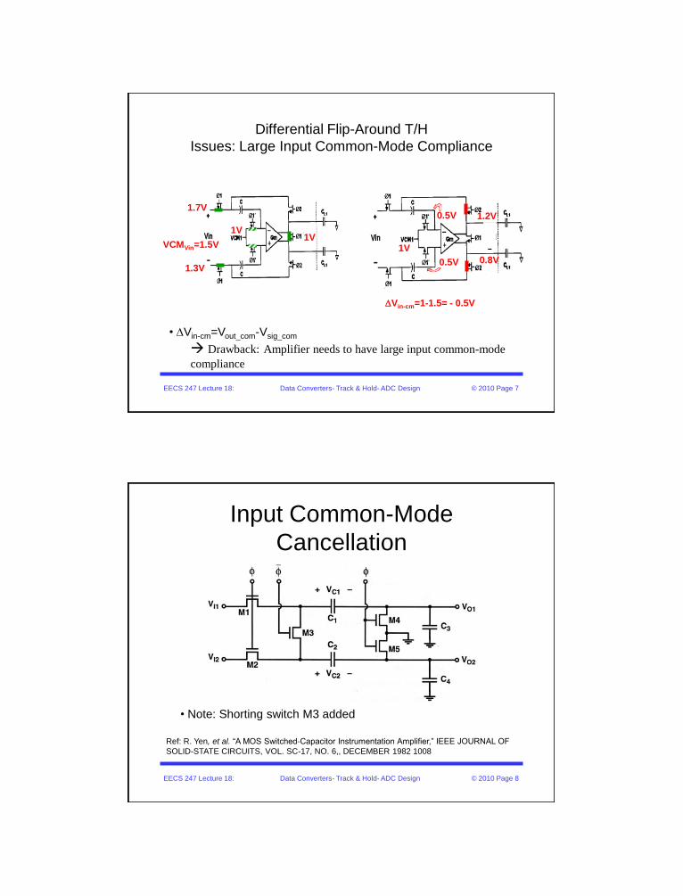
Differential Flip-Around T/H
Issues: Large Input Common-Mode Compliance
• DVin-cm=Vout_com-Vsig_com
Drawback: Amplifier needs to have large input common-mode
compliance
VCMVin=1.5V
1.7V
1.3V
1V1V
1V
1.2V
0.8V
0.5V
DVin-cm=1-1.5= - 0.5V
0.5V
EECS 247 Lecture 18: Data Converters- Track & Hold- ADC Design © 2010 Page 8
Input Common-Mode
Cancellation
Ref: R. Yen, et al. “A MOS Switched-Capacitor Instrumentation Amplifier,” IEEE JOURNAL OF
SOLID-STATE CIRCUITS, VOL. SC-17, NO. 6,, DECEMBER 1982 1008
• Note: Shorting switch M3 added
EECS 247 Lecture 18: Data Converters- Track & Hold- ADC Design © 2010 Page 9
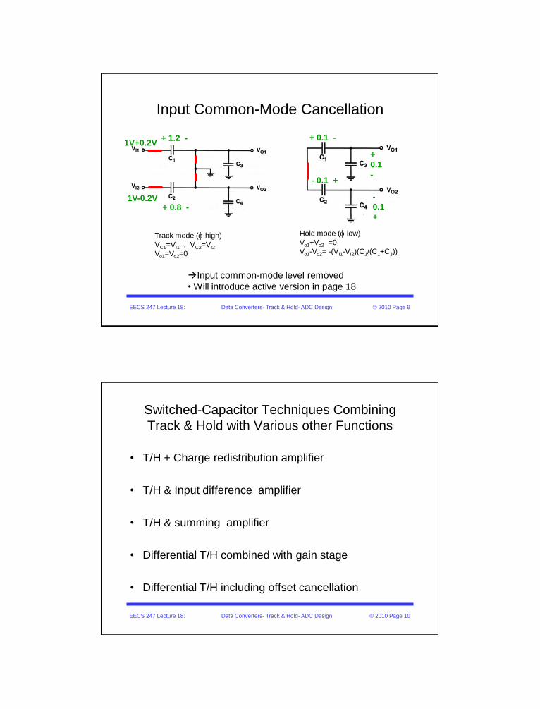
Input Common-Mode Cancellation
Track mode (f high)
VC1=VI1 , VC2=VI2
Vo1=Vo2=0
Hold mode (f low)
Vo1+Vo2 =0
Vo1-Vo2= -(VI1-VI2)(C1/(C1+C3))
Input common-mode level removed
• Will introduce active version in page 18
1V+0.2V
1V-0.2V
+ 1.2 -
+ 0.8 -
+ 0.1 -
- 0.1 +
+
0.1
-
-
0.1
+
EECS 247 Lecture 18: Data Converters- Track & Hold- ADC Design © 2010 Page 10
Switched-Capacitor Techniques Combining
Track & Hold with Various other Functions
• T/H + Charge redistribution amplifier
• T/H & Input difference amplifier
• T/H & summing amplifier
• Differential T/H combined with gain stage
• Differential T/H including offset cancellation
EECS 247 Lecture 18: Data Converters- Track & Hold- ADC Design © 2010 Page 11
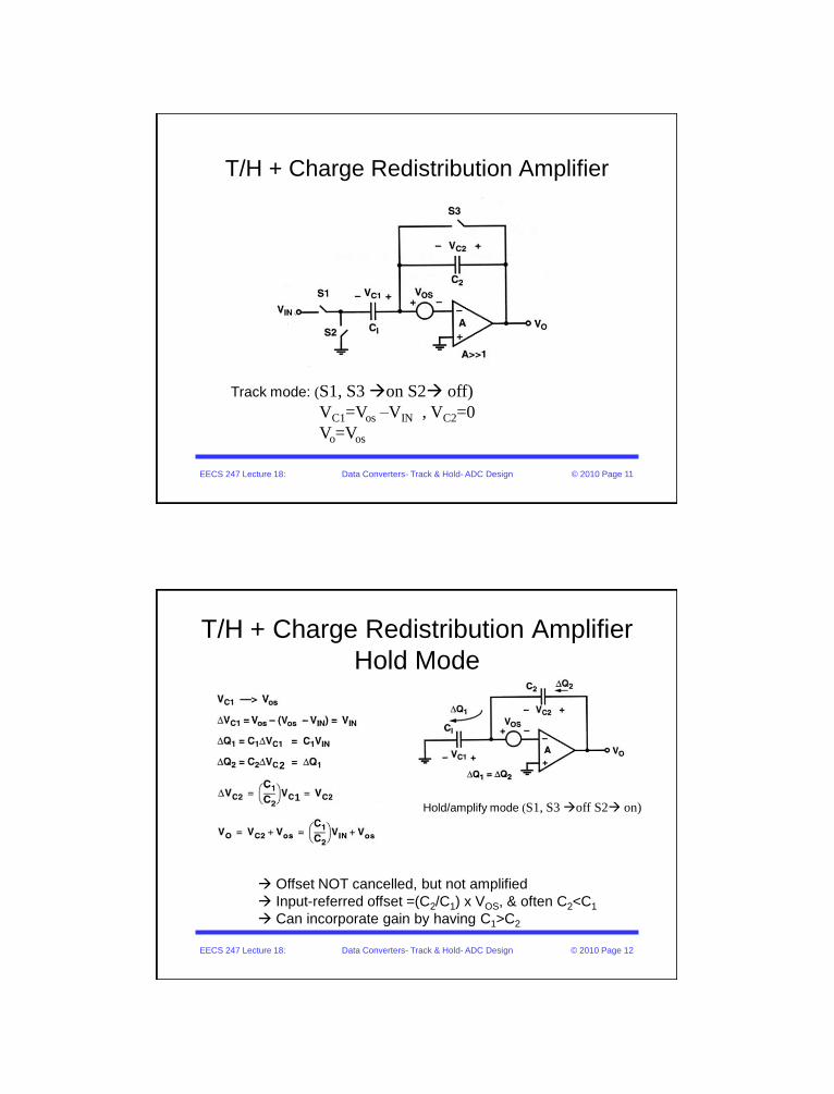
T/H + Charge Redistribution Amplifier
Track mode: (S1, S3 on S2 off)
VC1=Vos –VIN , VC2=0
Vo=Vos
EECS 247 Lecture 18: Data Converters- Track & Hold- ADC Design © 2010 Page 12
T/H + Charge Redistribution Amplifier
Hold Mode
Hold/amplify mode (S1, S3 off S2 on)
Offset NOT cancelled, but not amplified
Input-referred offset =(C2/C1) x VOS, & often C2<C1
Can incorporate gain by having C1>C2
2
1
2
EECS 247 Lecture 18: Data Converters- Track & Hold- ADC Design © 2010 Page 13
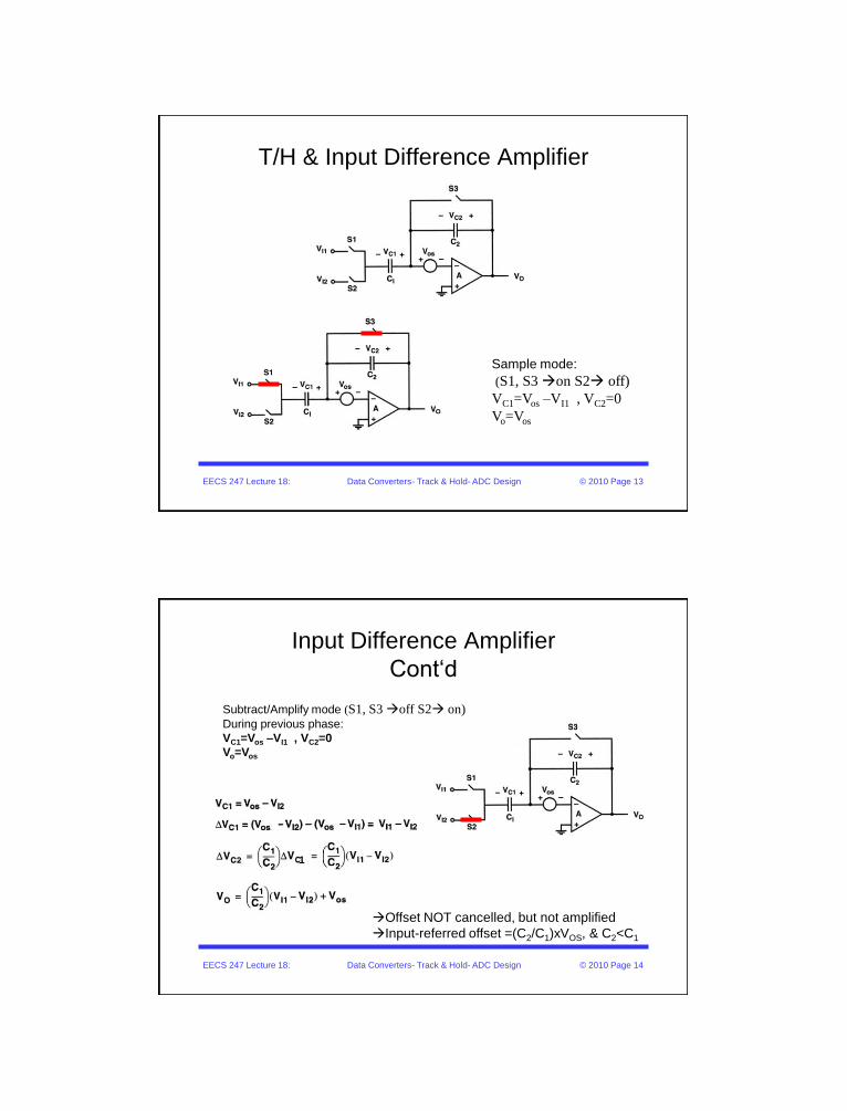
T/H & Input Difference Amplifier
Sample mode:
(S1, S3 on S2 off)
VC1=Vos –VI1 , VC2=0
Vo=Vos
EECS 247 Lecture 18: Data Converters- Track & Hold- ADC Design © 2010 Page 14
Input Difference Amplifier
Cont„d
Subtract/Amplify mode (S1, S3 off S2 on)During previous phase:
VC1=Vos –VI1 , VC2=0
Vo=Vos
1
Offset NOT cancelled, but not amplified
Input-referred offset =(C2/C1)xVOS, & C2<C1
EECS 247 Lecture 18: Data Converters- Track & Hold- ADC Design © 2010 Page 15
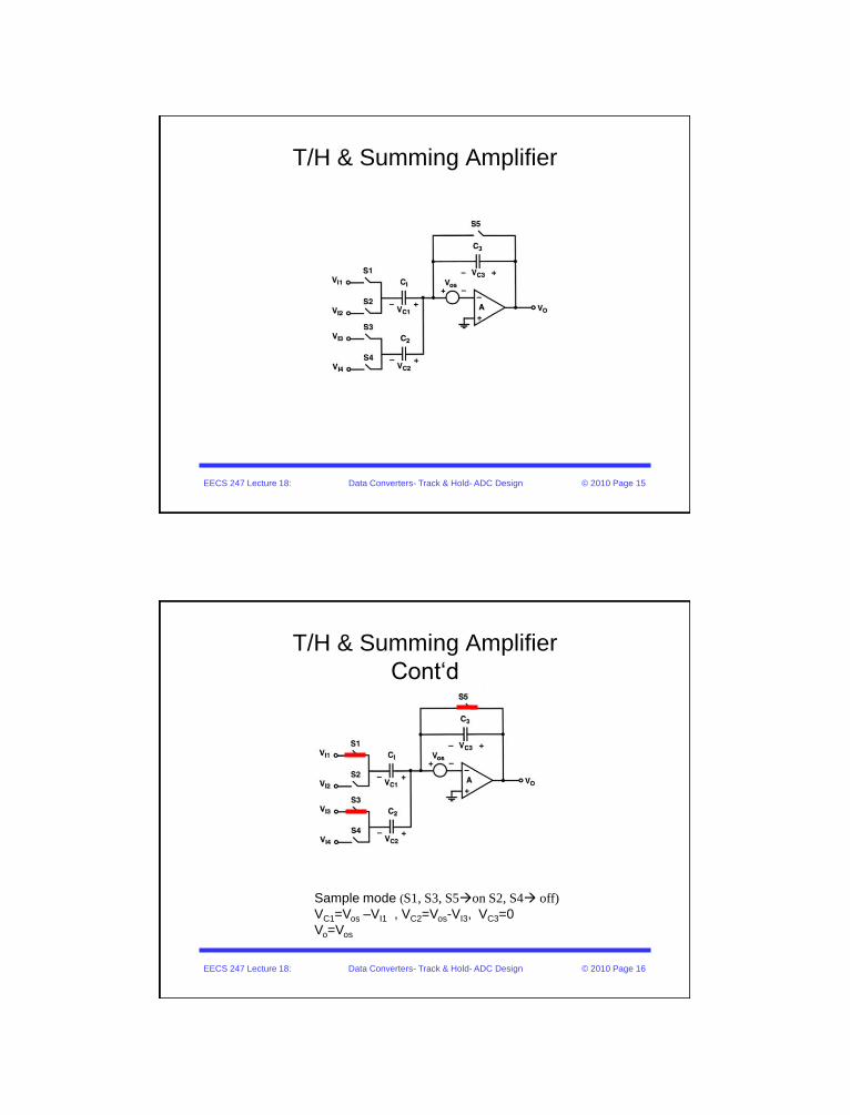
T/H & Summing Amplifier
EECS 247 Lecture 18: Data Converters- Track & Hold- ADC Design © 2010 Page 16
T/H & Summing Amplifier
Cont„d
Sample mode (S1, S3, S5on S2, S4 off)
VC1=Vos –VI1 , VC2=Vos-VI3, VC3=0
Vo=Vos
EECS 247 Lecture 18: Data Converters- Track & Hold- ADC Design © 2010 Page 17
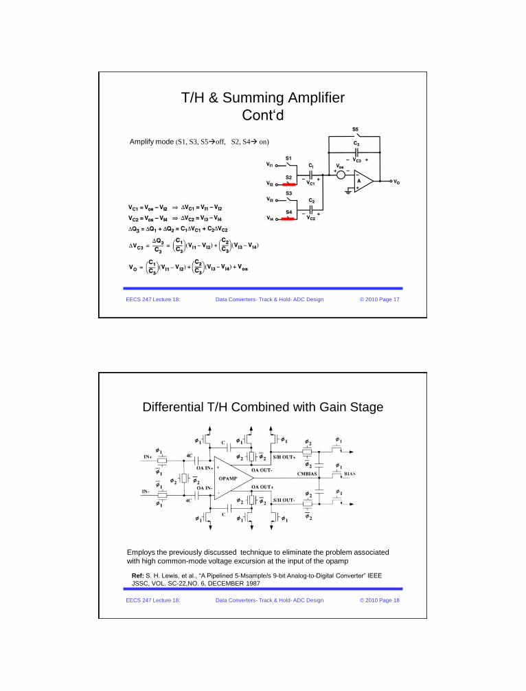
T/H & Summing Amplifier
Cont„d
Amplify mode (S1, S3, S5off, S2, S4 on)
3
EECS 247 Lecture 18: Data Converters- Track & Hold- ADC Design © 2010 Page 18
Differential T/H Combined with Gain Stage
Ref: S. H. Lewis, et al., “A Pipelined 5-Msample/s 9-bit Analog-to-Digital Converter” IEEE
JSSC, VOL. SC-22,NO. 6, DECEMBER 1987
Employs the previously discussed technique to eliminate the problem associated
with high common-mode voltage excursion at the input of the opamp
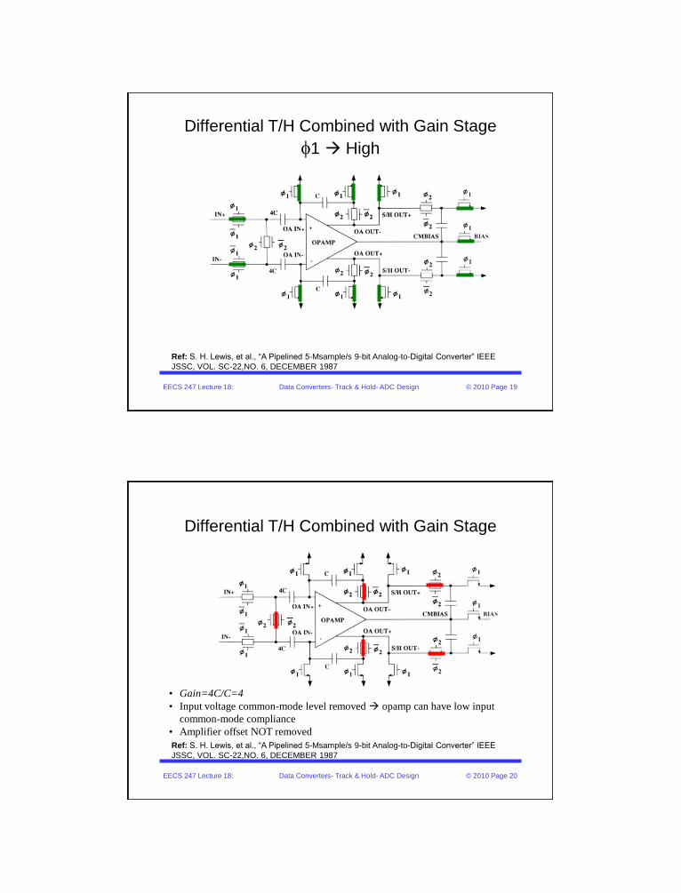
EECS 247 Lecture 18: Data Converters- Track & Hold- ADC Design © 2010 Page 19
Ref: S. H. Lewis, et al., “A Pipelined 5-Msample/s 9-bit Analog-to-Digital Converter” IEEE
JSSC, VOL. SC-22,NO. 6, DECEMBER 1987
Differential T/H Combined with Gain Stage
f1 High
EECS 247 Lecture 18: Data Converters- Track & Hold- ADC Design © 2010 Page 20
Ref: S. H. Lewis, et al., “A Pipelined 5-Msample/s 9-bit Analog-to-Digital Converter” IEEE
JSSC, VOL. SC-22,NO. 6, DECEMBER 1987
• Gain=4C/C=4
• Input voltage common-mode level removed opamp can have low input
common-mode compliance
• Amplifier offset NOT removed
Differential T/H Combined with Gain Stage
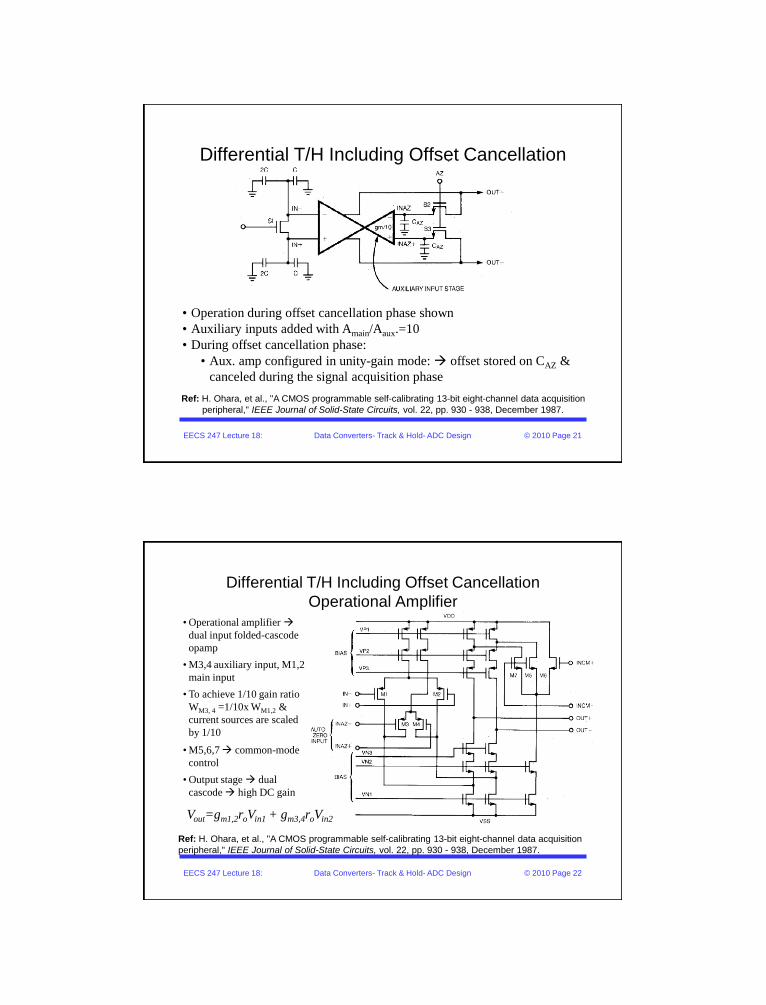
EECS 247 Lecture 18: Data Converters- Track & Hold- ADC Design © 2010 Page 21
Ref: H. Ohara, et al., "A CMOS programmable self-calibrating 13-bit eight-channel data acquisition
peripheral," IEEE Journal of Solid-State Circuits, vol. 22, pp. 930 - 938, December 1987.
• Operation during offset cancellation phase shown
• Auxiliary inputs added with Amain/Aaux.=10
• During offset cancellation phase:
• Aux. amp configured in unity-gain mode: offset stored on CAZ &
canceled during the signal acquisition phase
Differential T/H Including Offset Cancellation
EECS 247 Lecture 18: Data Converters- Track & Hold- ADC Design © 2010 Page 22
Differential T/H Including Offset Cancellation
Operational Amplifier
Ref: H. Ohara, et al., "A CMOS programmable self-calibrating 13-bit eight-channel data acquisition
peripheral," IEEE Journal of Solid-State Circuits, vol. 22, pp. 930 - 938, December 1987.
• Operational amplifier
dual input folded-cascode
opamp
• M3,4 auxiliary input, M1,2
main input
• To achieve 1/10 gain ratio
WM3, 4 =1/10x WM1,2 &
current sources are scaled
by 1/10
• M5,6,7 common-mode
control
• Output stage dual
cascode high DC gain
Vout=gm1,2roVin1 + gm3,4roVin2
EECS 247 Lecture 18: Data Converters- Track & Hold- ADC Design © 2010 Page 23
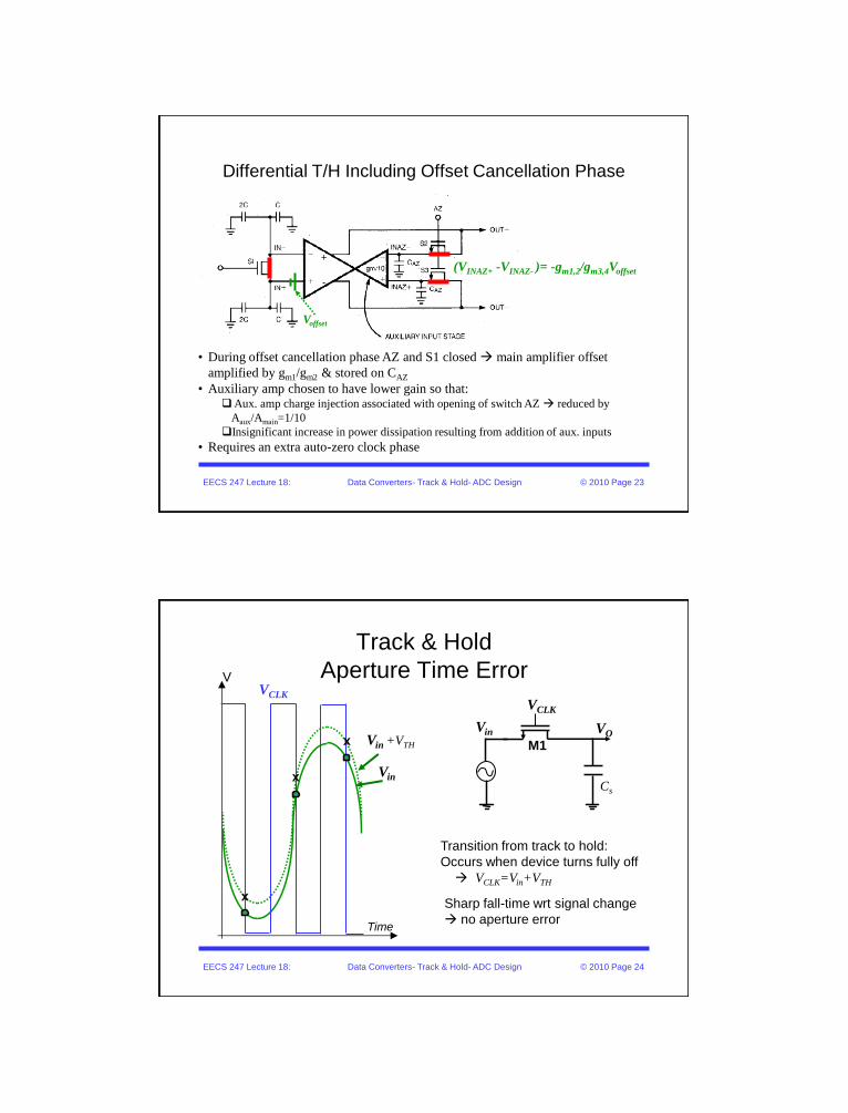
• During offset cancellation phase AZ and S1 closed main amplifier offset
amplified by gm1/gm2 & stored on CAZ
• Auxiliary amp chosen to have lower gain so that:Aux. amp charge injection associated with opening of switch AZ reduced by
Aaux/Amain=1/10
Insignificant increase in power dissipation resulting from addition of aux. inputs
• Requires an extra auto-zero clock phase
Differential T/H Including Offset Cancellation Phase
Voffset
+
-
(VINAZ+ -VINAZ- )= -gm1,2/gm3,4Voffset
EECS 247 Lecture 18: Data Converters- Track & Hold- ADC Design © 2010 Page 24
Track & Hold
Aperture Time Error
Time
V
Vin VO
M1
VCLK
Vin
Vin +VTH
VCLK
Transition from track to hold:
Occurs when device turns fully off
VCLK=Vin+VTH
Sharp fall-time wrt signal change
no aperture error
Cs
x
x
x
EECS 247 Lecture 18: Data Converters- Track & Hold- ADC Design © 2010 Page 25
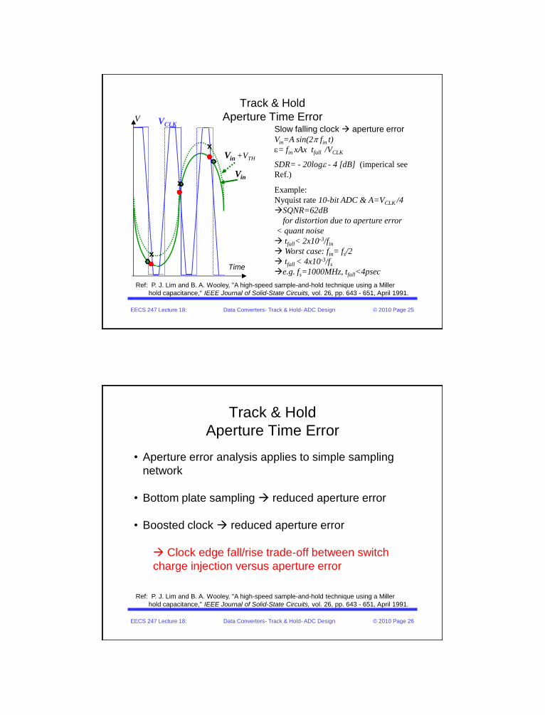
Track & Hold
Aperture Time Error
Time
V
Slow falling clock aperture error
Vin=A sin(2p fin t)
= fin xAx tfall /VCLK
SDR= - 20log - 4 [dB] (imperical see
Ref.)
Example:
Nyquist rate 10-bit ADC & A=VCLK /4
SQNR=62dB
for distortion due to aperture error
< quant noise
tfall< 2x10⁻³/fin
Worst case: fin= fs/2
tfall < 4x10⁻³/fs
e.g. fs=1000MHz, tfall<4psec
Vin
Vin +VTH
VCLK
Ref: P. J. Lim and B. A. Wooley, "A high-speed sample-and-hold technique using a Miller
hold capacitance," IEEE Journal of Solid-State Circuits, vol. 26, pp. 643 - 651, April 1991.
x
x
x
EECS 247 Lecture 18: Data Converters- Track & Hold- ADC Design © 2010 Page 26
Track & Hold
Aperture Time Error
• Aperture error analysis applies to simple sampling
network
• Bottom plate sampling reduced aperture error
• Boosted clock reduced aperture error
Clock edge fall/rise trade-off between switch
charge injection versus aperture error
Ref: P. J. Lim and B. A. Wooley, "A high-speed sample-and-hold technique using a Miller
hold capacitance," IEEE Journal of Solid-State Circuits, vol. 26, pp. 643 - 651, April 1991.
EECS 247 Lecture 18: Data Converters- Track & Hold- ADC Design © 2010 Page 27
ADC
Architecture & Design
EECS 247 Lecture 18: Data Converters- Track & Hold- ADC Design © 2010 Page 28
ADC Architectures
• Slope type converters
• Successive approximation
• Flash
• Time-interleaved / parallel converter
• Folding
• Residue type ADCs– Two-step
– Pipeline
– …
• Oversampled ADCs
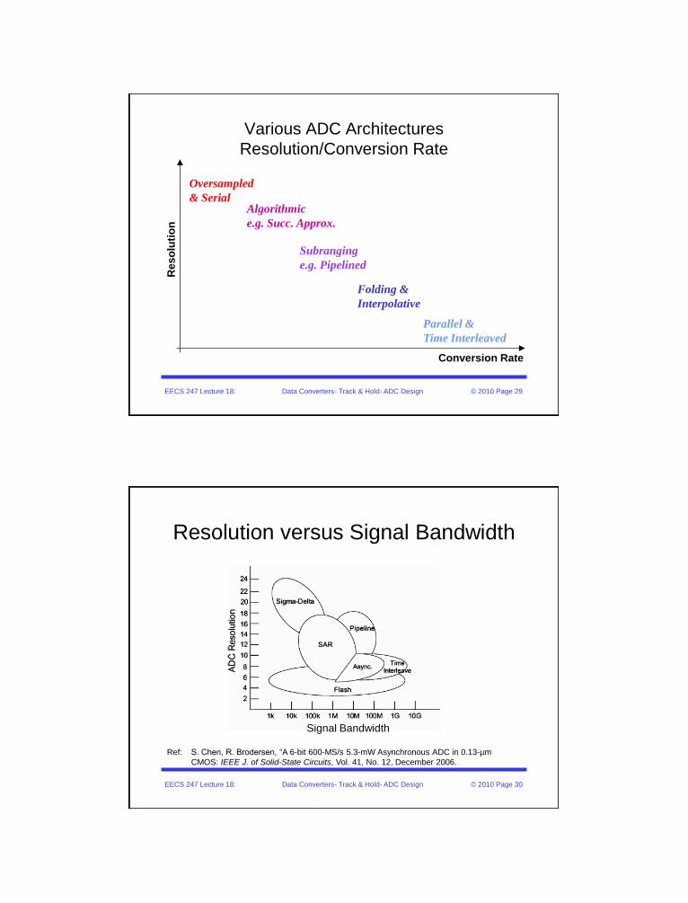
EECS 247 Lecture 18: Data Converters- Track & Hold- ADC Design © 2010 Page 29
Conversion Rate
Re
so
luti
on
Oversampled
& Serial Algorithmic
e.g. Succ. Approx.
Subranging
e.g. Pipelined
Folding &
Interpolative
Parallel &
Time Interleaved
Various ADC Architectures
Resolution/Conversion Rate
Resolution versus Signal Bandwidth
EECS 247 Lecture 18: Data Converters- Track & Hold- ADC Design © 2010 Page 30
Ref: S. Chen, R. Brodersen, “A 6-bit 600-MS/s 5.3-mW Asynchronous ADC in 0.13-µm
CMOS: IEEE J. of Solid-State Circuits, Vol. 41, No. 12, December 2006.
Signal Bandwidth
EECS 247 Lecture 18: Data Converters- Track & Hold- ADC Design © 2010 Page 31
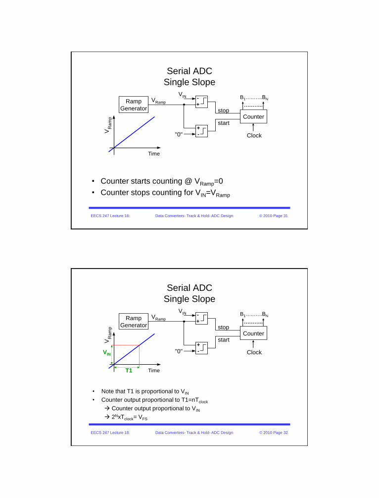
Serial ADC
Single Slope
• Counter starts counting @ VRamp=0
• Counter stops counting for VIN=VRamp
Ramp
Generator
Time
VR
am
p
VRamp
VIN
"0"
Counterstop
start
Clock
B1…..…..BN
………..
-
+
+
-
EECS 247 Lecture 18: Data Converters- Track & Hold- ADC Design © 2010 Page 32
Serial ADC
Single Slope
• Note that T1 is proportional to VIN
• Counter output proportional to T1=nTclock
Counter output proportional to VIN
2NxTclock= VFS
Ramp
Generator
Time
VR
am
p
VRamp
VIN
"0"
Counterstop
start
Clock
B1…..…..BN
………..
-
+
+
-
T1
VIN
EECS 247 Lecture 18: Data Converters- Track & Hold- ADC Design © 2010 Page 33
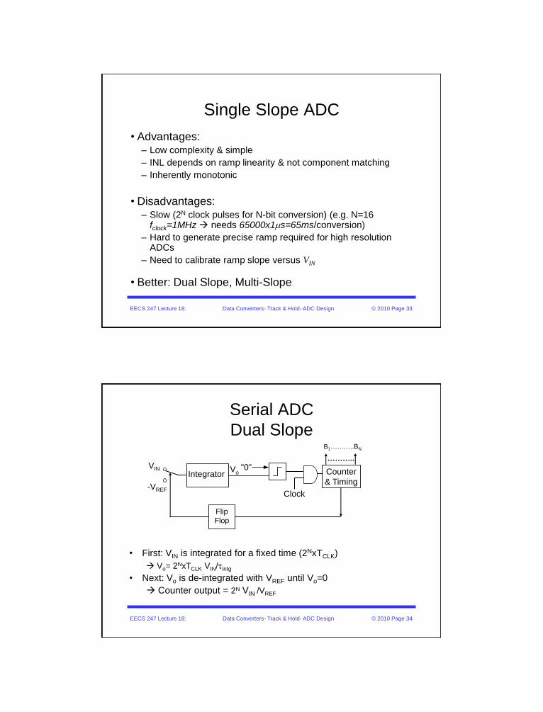
Single Slope ADC
• Advantages:– Low complexity & simple
– INL depends on ramp linearity & not component matching
– Inherently monotonic
• Disadvantages:– Slow (2N clock pulses for N-bit conversion) (e.g. N=16
fclock=1MHz needs 65000x1ms=65ms/conversion)
– Hard to generate precise ramp required for high resolution ADCs
– Need to calibrate ramp slope versus VIN
• Better: Dual Slope, Multi-Slope
EECS 247 Lecture 18: Data Converters- Track & Hold- ADC Design © 2010 Page 34
Serial ADC
Dual Slope
• First: VIN is integrated for a fixed time (2NxTCLK)
Vo= 2NxTCLK VIN/tintg
• Next: Vo is de-integrated with VREF until Vo=0
Counter output = 2N VIN /VREF
Integrator
Flip
Flop
VoVIN "0"
Counter
& Timing
Clock
B1………..BN
………..
-VREF
EECS 247 Lecture 18: Data Converters- Track & Hold- ADC Design © 2010 Page 35
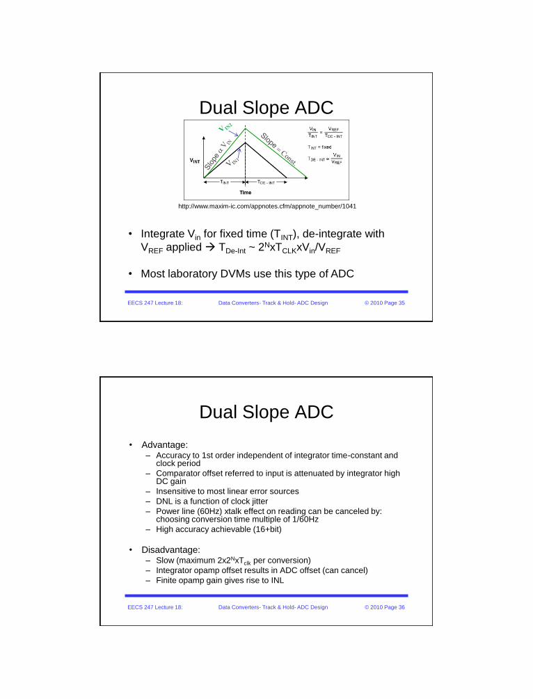
Dual Slope ADC
http://www.maxim-ic.com/appnotes.cfm/appnote_number/1041
• Integrate Vin for fixed time (TINT), de-integrate with
VREF applied TDe-Int ~ 2NxTCLKxVin/VREF
• Most laboratory DVMs use this type of ADC
EECS 247 Lecture 18: Data Converters- Track & Hold- ADC Design © 2010 Page 36
Dual Slope ADC
• Advantage:– Accuracy to 1st order independent of integrator time-constant and
clock period
– Comparator offset referred to input is attenuated by integrator high DC gain
– Insensitive to most linear error sources
– DNL is a function of clock jitter
– Power line (60Hz) xtalk effect on reading can be canceled by: choosing conversion time multiple of 1/60Hz
– High accuracy achievable (16+bit)
• Disadvantage:– Slow (maximum 2x2NxTclk per conversion)
– Integrator opamp offset results in ADC offset (can cancel)
– Finite opamp gain gives rise to INL
EECS 247 Lecture 18: Data Converters: Flash ADC & Comparator Design © 2010 Page 37
ADC Architectures
• Slope type converters
• Successive approximation
• Flash
• Time-interleaved / parallel converter
• Folding
• Residue type ADCs– Two-step
– Pipeline
– …
• Oversampled ADCs
EECS 247 Lecture 18: Data Converters- Track & Hold- ADC Design © 2010 Page 38
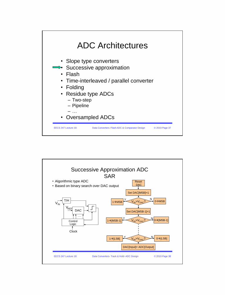
Successive Approximation ADC
SAR• Algorithmic type ADC
• Based on binary search over DAC output
Reset
DAC
Set DAC[MSB]=1
VIN>VDAC?1MSB 0MSB
Set DAC[MSB-1]=1
VIN>VDAC?1[MSB-1] 0[MSB-1]
.
.
.
.
.
.
VIN>VDAC?1[LSB] 0[LSB]
DAC[Input]= ADC[Output]
Y
Y
Y
N
N
N
DAC
VIN
ControlLogic
Clock
VREF
T/H
EECS 247 Lecture 18: Data Converters- Track & Hold- ADC Design © 2010 Page 39
Successive Approximation ADC
• High accuracy achievable (16+ Bits)
• Need DAC to be accurate enough
• Require N clock cycles for N-bit conversion (much faster than slope type)
• Moderate speed (highest SAR conversion rate 2Ms/sec & 18bits)
VDAC/VREF
Time / Clock Ticks
1
1/2
3/4
5/8VIN
1/2 3/4 5/8 11/16 21/32 41/64
Example: 6-bit ADC & VIN=5/8VREF
ADC101000
DAC
VIN
ControlLogic
Clock
VREF
T/H
Test
MSB
Test
MSB-1
DAC
Output
+
-
EECS 247 Lecture 18: Data Converters- Track & Hold- ADC Design © 2010 Page 40
Example: SAR ADC
Charge Redistribution Type
• Built with binary weighted capacitors, switches,
comparator & control logic
• T/H inherent in DAC
C2C4C8C32C
Out
Stop
b1b2b3
b4 (MSB)
-
Comparator
16C
b3
C
VinVREF
VinControl
LogicTo
switches
b0
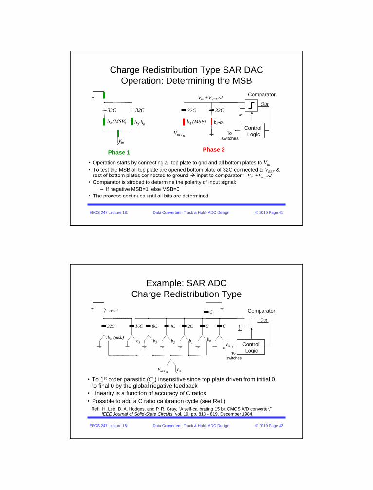
EECS 247 Lecture 18: Data Converters- Track & Hold- ADC Design © 2010 Page 41
Charge Redistribution Type SAR DAC
Operation: Determining the MSB
• Operation starts by connecting all top plate to gnd and all bottom plates to Vin
• To test the MSB all top plate are opened bottom plate of 32C connected to VREF & rest of bottom plates connected to ground input to comparator= -Vin +VREF/2
• Comparator is strobed to determine the polarity of input signal:
– If negative MSB=1, else MSB=0
• The process continues until all bits are determined
32C
Out
b4 (MSB)
-
Comparator
32C
b3-b0
Vin
VREF
Control
LogicTo
switches
32C
b4 (MSB)
32C
b3-b0
-Vin +VREF /2
Phase 1Phase 2
EECS 247 Lecture 18: Data Converters- Track & Hold- ADC Design © 2010 Page 42
Example: SAR ADC
Charge Redistribution Type
• To 1st order parasitic (Cp) insensitive since top plate driven from initial 0 to final 0 by the global negative feedback
• Linearity is a function of accuracy of C ratios
• Possible to add a C ratio calibration cycle (see Ref.)
C2C4C8C32C
Out
reset
b1b2b3
b4 (msb)
CP
-
Comparator
16C
b3
C
VinVREF
Vin Control
LogicTo
switches
Ref: H. Lee, D. A. Hodges, and P. R. Gray, "A self-calibrating 15 bit CMOS A/D converter,"
IEEE Journal of Solid-State Circuits, vol. 19, pp. 813 - 819, December 1984.
b0
EECS 247 Lecture 18: Data Converters: Flash ADC & Comparator Design © 2010 Page 43
ADC Architectures
• Slope type converters
• Successive approximation
• Flash
• Time-interleaved / parallel converter
• Folding
• Residue type ADCs– Two-step
– Pipeline
– …
• Oversampled ADCs
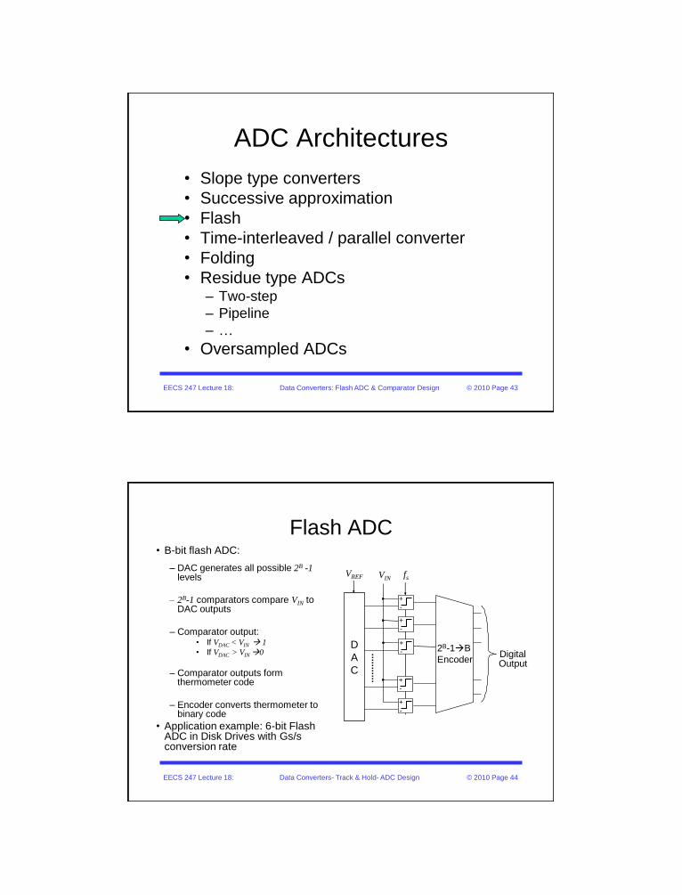
EECS 247 Lecture 18: Data Converters- Track & Hold- ADC Design © 2010 Page 44
Flash ADC• B-bit flash ADC:
– DAC generates all possible 2B -1levels
– 2B-1 comparators compare VIN to DAC outputs
– Comparator output:• If VDAC < VIN 1
• If VDAC > VIN 0
– Comparator outputs form thermometer code
– Encoder converts thermometer to binary code
• Application example: 6-bit Flash ADC in Disk Drives with Gs/s conversion rate
DigitalOutput
D
A
C
2B-1B
Encoder
VREF VIN fs
+
-
+
-
+
-
+
-
+
-
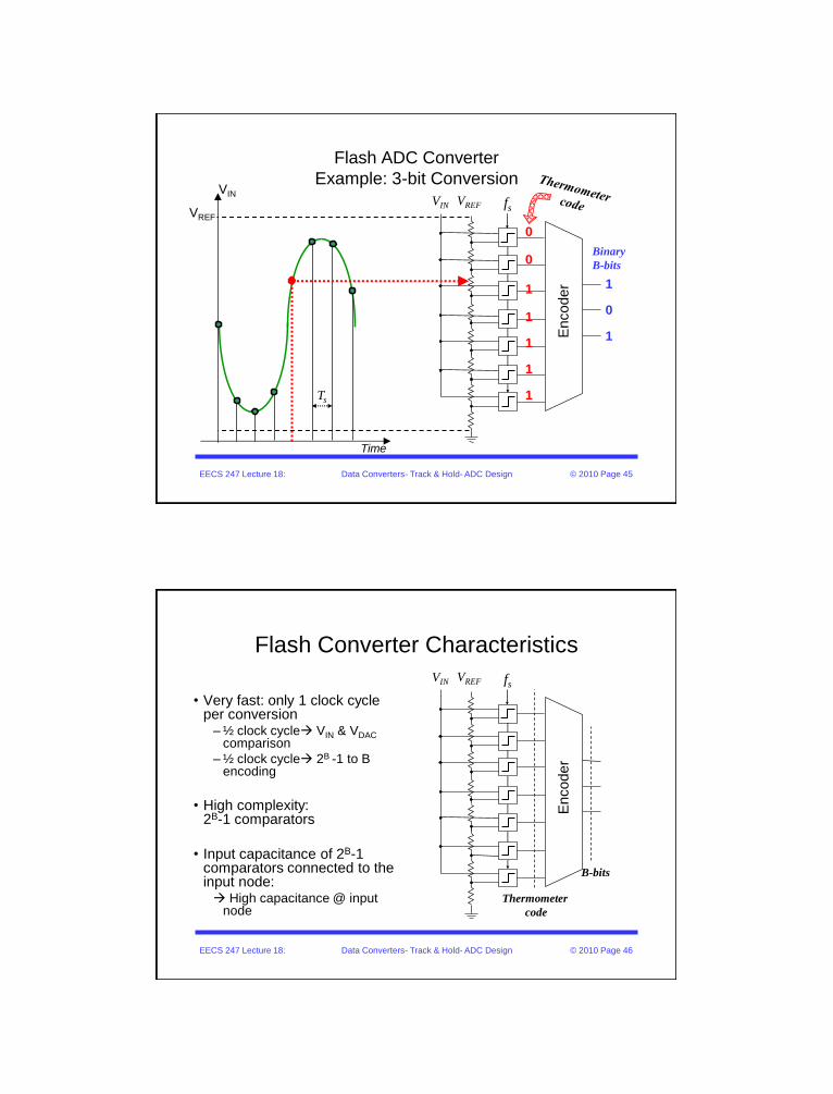
EECS 247 Lecture 18: Data Converters- Track & Hold- ADC Design © 2010 Page 45
Flash ADC Converter
Example: 3-bit Conversion
Encoder
fs
Binary
B-bits
Time
VREF
0
0
1
1
1
1
1
1
0
1
VINVIN VREF
Ts
EECS 247 Lecture 18: Data Converters- Track & Hold- ADC Design © 2010 Page 46
Flash Converter Characteristics
• Very fast: only 1 clock cycle per conversion
– ½ clock cycle VIN & VDACcomparison
– ½ clock cycle 2B -1 to B encoding
• High complexity: 2B-1 comparators
• Input capacitance of 2B-1 comparators connected to the input node: High capacitance @ input
node
Encoder
fsVIN VREF
Thermometer
code
B-bits
Flash ADC Converter Considerations
EECS 247 Lecture 18: Data Converters- Track & Hold- ADC Design © 2010 Page 47
M1 M2
IS
Vref
-Vo+
Vin
fs
R/2
R
R
R
R/2
R
Encoder Digital
Output
VINV
REF fs
.....
Assume simple comparator design
Depending on Vin level xn lower comparators
have M1 on & M2 off xm upper comparators
have M1 off & M2 (m+n=2B-1)
Total capacitance experienced by input source
a function of Vin
Also note Vin feedthrough to Vref taps via M1
& M2 G-S capacitance & Rs
When switches Mx open, charge injection and
clock feedthru causes perturbation on R taps
Mx
EECS 247 Lecture 18: Data Converters: Flash ADC & Comparator Design © 2010 Page 48
Flash Converter Sources of Error
• Comparator input:
– DC offset
– Nonlinear input capacitance
– Feedthrough of input signal to reference ladder
– Kickback noise (disturbs reference)
– Signal dependent sampling time (addition of T/H @ the input eliminates this problem)
• Comparator output:
– Sparkle codes (… 0001011111)
– Metastability
R/2
R
R
R
R/2
R
Encoder Digital
Output
VINV
REF fs
.....
EECS 247 Lecture 18: Data Converters: Flash ADC & Comparator Design © 2010 Page 49
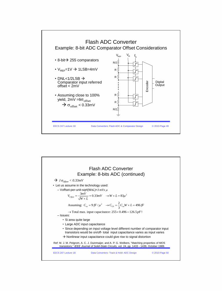
Flash ADC ConverterExample: 8-bit ADC Comparator Offset Considerations
• 8-bit 255 comparators
• VREF=1V 1LSB=4mV
• DNL<1/2LSB Comparator input referred offset < 2mV
• Assuming close to 100% yield, 2mV =6soffset
soffset < 0.33mV
R/2
R
R
R
R/2
R
Encoder Digital
Output
VINV
REF fs
.....
EECS 247 Lecture 18: Data Converters- Track & Hold- ADC Design © 2010 Page 50
Flash ADC Converter
Example: 8-bits ADC (continued)
1sOffset < 0.33mV
• Let us assume in the technology used:
– Voffset-per-unit-sqrt(WxL)=3 mVx m
– Issues:
• Si area quite large
• Large ADC input capacitance
• Since depending on input voltage level different number of comparator input
transistors would be on/off- total input capacitance varies as input varies
Nonlinear input capacitance could give rise to signal distortion
2
0
2
30.33 83
2Assuming: 9 / 496
3
Total max. input capacitance: 255 0.496 126.5 !
ffset
ox GS ox
mVV mV W L
W L
C fF C C W L fF
pF
m
m
Ref: M. J. M. Pelgrom, A. C. J. Duinmaijer, and A. P. G. Welbers, "Matching properties of MOS
transistors," IEEE Journal of Solid-State Circuits, vol. 24, pp. 1433 - 1439, October 1989.
EECS 247 Lecture 18: Data Converters: Flash ADC & Comparator Design © 2010 Page 51
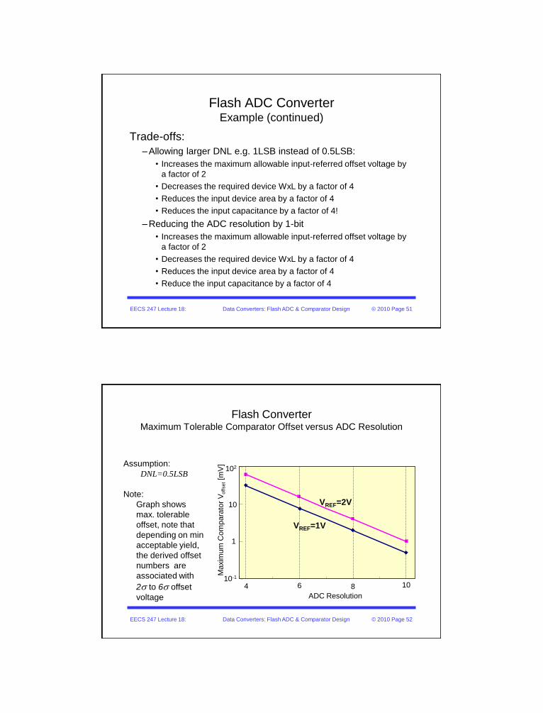
Flash ADC ConverterExample (continued)
Trade-offs:
– Allowing larger DNL e.g. 1LSB instead of 0.5LSB:
• Increases the maximum allowable input-referred offset voltage by
a factor of 2
• Decreases the required device WxL by a factor of 4
• Reduces the input device area by a factor of 4
• Reduces the input capacitance by a factor of 4!
– Reducing the ADC resolution by 1-bit
• Increases the maximum allowable input-referred offset voltage by
a factor of 2
• Decreases the required device WxL by a factor of 4
• Reduces the input device area by a factor of 4
• Reduce the input capacitance by a factor of 4
EECS 247 Lecture 18: Data Converters: Flash ADC & Comparator Design © 2010 Page 52
Flash ConverterMaximum Tolerable Comparator Offset versus ADC Resolution
10-1
1
10
102
4 6 8 10
VREF=1V
VREF=2V
Assumption:
DNL=0.5LSB
Note:
Graph shows
max. tolerable
offset, note that
depending on min
acceptable yield,
the derived offset
numbers are
associated with
2s to 6s offset
voltage ADC Resolution
Maxim
um
Com
para
tor
Voff
set[m
V]
EECS 247 Lecture 18: Data Converters: Flash ADC & Comparator Design © 2010 Page 53
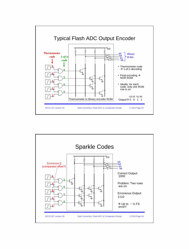
Typical Flash ADC Output Encoder
0
0
1
1
1
0
1
0
0
Thermometer to Binary encoder ROM
VDD
• Thermometer code 1-of-n decoding
• Final encoding NOR ROM
• Ideally, for each code, only one ROM row is on
b3b2b1b0
b3 b2 b1 b0
Output 0 0 1 1
Thermometer
codeBinary
B-bits1-of-n
code
EECS 247 Lecture 18: Data Converters: Flash ADC & Comparator Design © 2010 Page 54
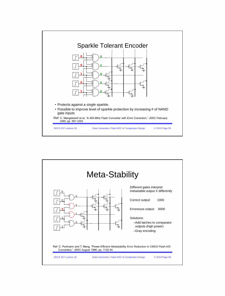
Sparkle Codes
Correct Output:1000
Problem: Two rows are on
Erroneous Output:
1110
Up to ~ ½ FS error!!
0
1
0
1
1
1
0
1
0
Erroneous 0
(comparator offset?)
VDD
b3b2b1b0
EECS 247 Lecture 18: Data Converters: Flash ADC & Comparator Design © 2010 Page 55
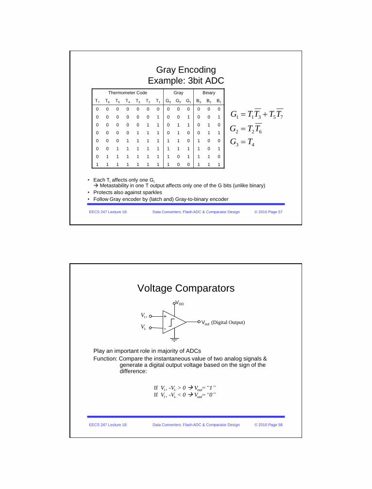
Sparkle Tolerant Encoder
Ref: C. Mangelsdorf et al, “A 400-MHz Flash Converter with Error Correction,” JSSC February 1990, pp. 997-1002
0
0
1
0
1
0
1
0
0
0
• Protects against a single sparkle.
• Possible to improve level of sparkle protection by increasing # of NAND gate inputs
EECS 247 Lecture 18: Data Converters: Flash ADC & Comparator Design © 2010 Page 56
Meta-Stability
Different gates interpret
metastable output X differently
Correct output: 1000
Erroneous output: 0000
Solutions:
–Add latches to comparator
outputs (high power)
–Gray encoding
Ref: C. Portmann and T. Meng, “Power-Efficient Metastability Error Reduction in CMOS Flash A/D
Converters,” JSSC August 1996, pp. 1132-40
0
0
X
1
1
0
1
1
0
EECS 247 Lecture 18: Data Converters: Flash ADC & Comparator Design © 2010 Page 57
Gray Encoding
Example: 3bit ADC
• Each Ti affects only one Gi
Metastability in one T output affects only one of the G bits (unlike binary)
• Protects also against sparkles
• Follow Gray encoder by (latch and) Gray-to-binary encoder
Thermometer Code Gray Binary
T7 T6 T5 T4 T3 T2 T1 G3 G2 G1 B3 B2 B1
0 0 0 0 0 0 0 0 0 0 0 0 0
0 0 0 0 0 0 1 0 0 1 0 0 1
0 0 0 0 0 1 1 0 1 1 0 1 0
0 0 0 0 1 1 1 0 1 0 0 1 1
0 0 0 1 1 1 1 1 1 0 1 0 0
0 0 1 1 1 1 1 1 1 1 1 0 1
0 1 1 1 1 1 1 1 0 1 1 1 0
1 1 1 1 1 1 1 1 0 0 1 1 1
43
622
75311
TG
TTG
TTTTG
EECS 247 Lecture 18: Data Converters: Flash ADC & Comparator Design © 2010 Page 58
Voltage Comparators
Play an important role in majority of ADCs
Function: Compare the instantaneous value of two analog signals & generate a digital output voltage based on the sign of the difference:
+
-
Vout (Digital Output)
VDD
If Vi+ -Vi- > 0 Vout=“1”
If Vi+ -Vi- < 0 Vout=“0”
Vi+
Vi-
EECS 247 Lecture 18: Data Converters: Flash ADC & Comparator Design © 2010 Page 59
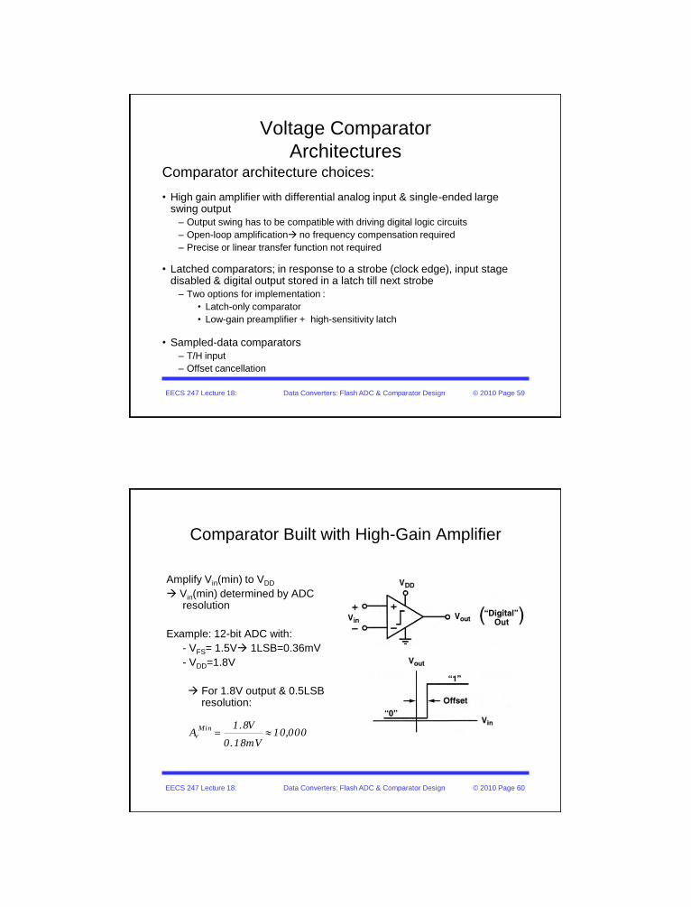
Voltage Comparator
ArchitecturesComparator architecture choices:
• High gain amplifier with differential analog input & single-ended large swing output
– Output swing has to be compatible with driving digital logic circuits
– Open-loop amplification no frequency compensation required
– Precise or linear transfer function not required
• Latched comparators; in response to a strobe (clock edge), input stage disabled & digital output stored in a latch till next strobe
– Two options for implementation :
• Latch-only comparator
• Low-gain preamplifier + high-sensitivity latch
• Sampled-data comparators
– T/H input
– Offset cancellation
EECS 247 Lecture 18: Data Converters: Flash ADC & Comparator Design © 2010 Page 60
Comparator Built with High-Gain Amplifier
Amplify Vin(min) to VDD
Vin(min) determined by ADC resolution
Example: 12-bit ADC with:
- VFS= 1.5V 1LSB=0.36mV
- VDD=1.8V
For 1.8V output & 0.5LSB resolution:
Minv
1.8VA 10,000
0.18mV
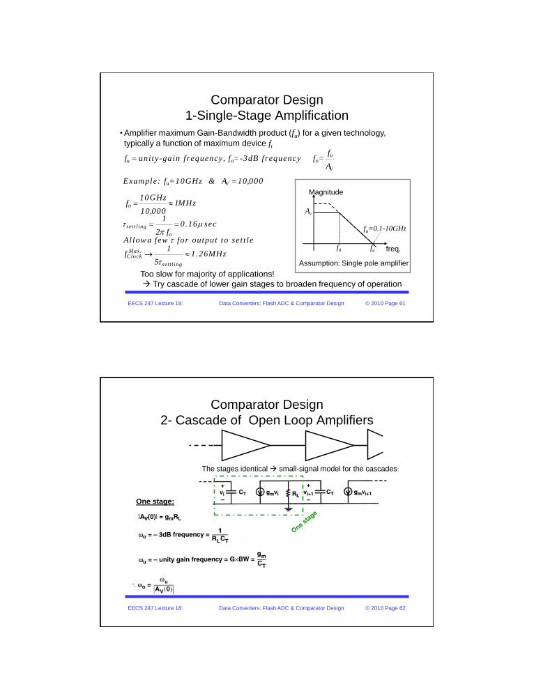
EECS 247 Lecture 18: Data Converters: Flash ADC & Comparator Design © 2010 Page 61
Comparator Design
1-Single-Stage Amplification
Too slow for majority of applications!
Try cascade of lower gain stages to broaden frequency of operation
Assumption: Single pole amplifier
• Amplifier maximum Gain-Bandwidth product (fu) for a given technology,
typically a function of maximum device ft
uu o o
V
u V
o
set t l ing
o
Max.Clock
set t l ing
ff uni ty-gain frequency, f =-3dB frequency f =
A
Example: f =10GHz & A 10,000
10GHz f 1MHz
10,0001
0.16 sec2 f
Al low a few for output to set t le 1
f 1.26MHz5
t mp
t
t
fu=0.1-10GHz
f0 fu freq.
Magnitude
Av
EECS 247 Lecture 18: Data Converters: Flash ADC & Comparator Design © 2010 Page 62
Comparator Design
2- Cascade of Open Loop Amplifiers
The stages identical small-signal model for the cascades:
One stage:
EECS 247 Lecture 18: Data Converters: Flash ADC & Comparator Design © 2010 Page 63
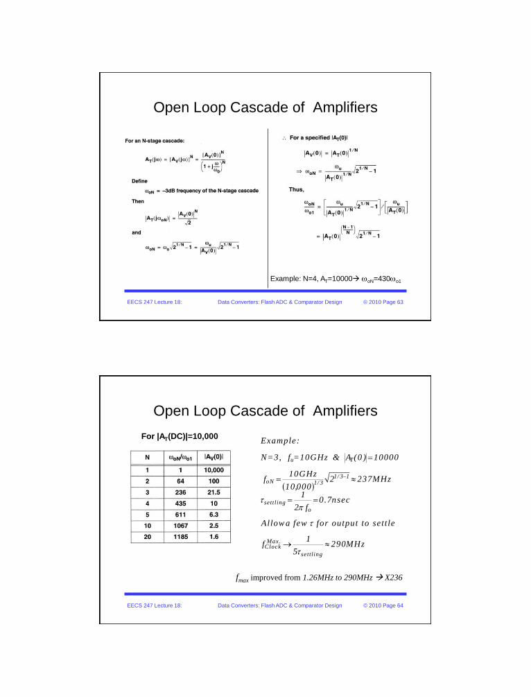
Open Loop Cascade of Amplifiers
Example: N=4, AT=10000 woN=430wo1
EECS 247 Lecture 18: Data Converters: Flash ADC & Comparator Design © 2010 Page 64
Open Loop Cascade of Amplifiers
For |AT(DC)|=10,000
u T
1/ 3 1oN 1/ 3
settling
o
Max.Clock
settling
Example:
N=3, f =10GHz & A (0 ) 10000
10GHz f 2 237MHz
10,0001
0.7nsec2 f
Allow a few for output to settle
1f 290MHz
5
tp
t
t
fmax improved from 1.26MHz to 290MHz X236
EECS 247 Lecture 18: Data Converters: Flash ADC & Comparator Design © 2010 Page 65
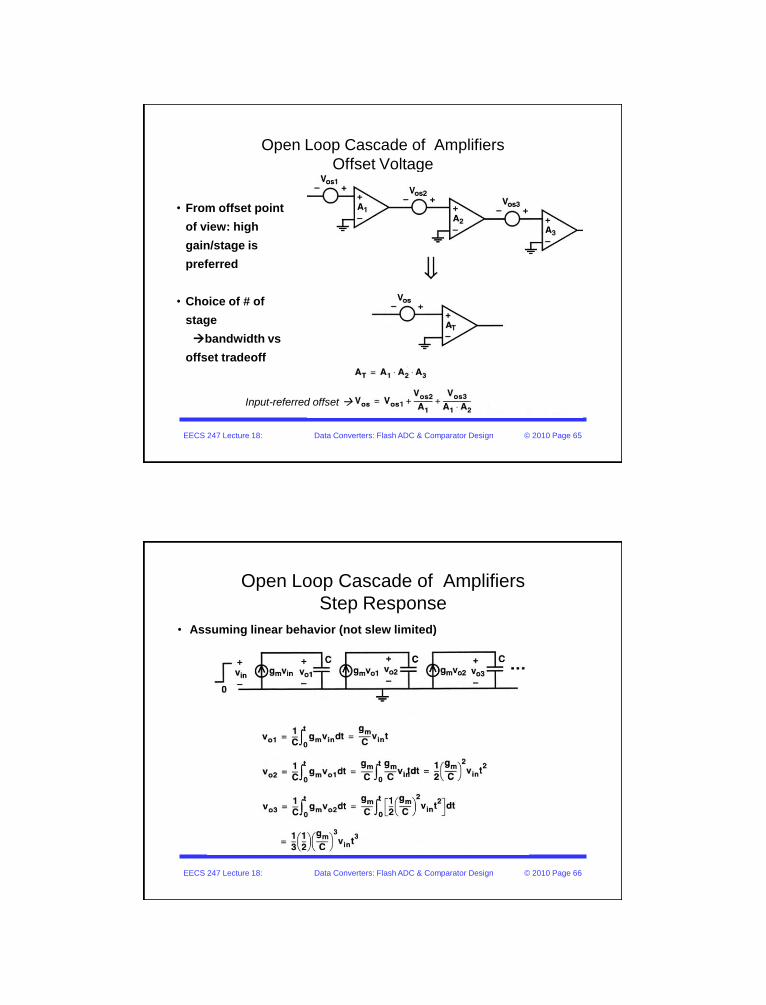
Open Loop Cascade of Amplifiers
Offset Voltage
• From offset point
of view: high
gain/stage is
preferred
• Choice of # of
stage
bandwidth vs
offset tradeoff
Input-referred offset
EECS 247 Lecture 18: Data Converters: Flash ADC & Comparator Design © 2010 Page 66
Open Loop Cascade of Amplifiers
Step Response
• Assuming linear behavior (not slew limited)
t
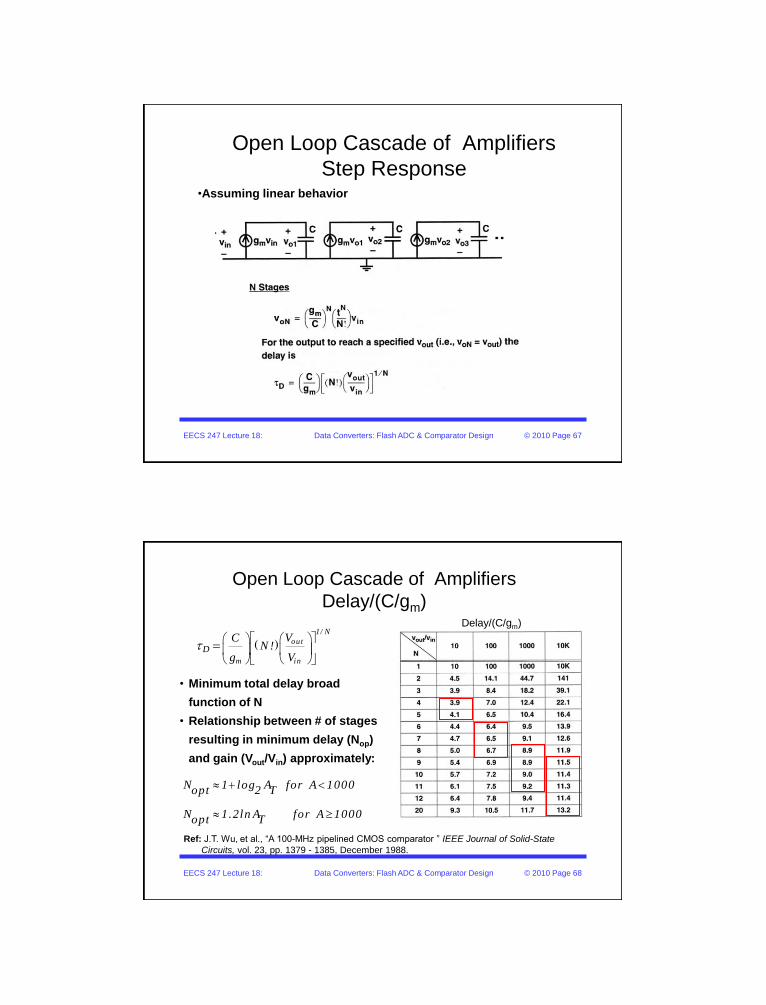
EECS 247 Lecture 18: Data Converters: Flash ADC & Comparator Design © 2010 Page 67
Open Loop Cascade of Amplifiers
Step Response•Assuming linear behavior
EECS 247 Lecture 18: Data Converters: Flash ADC & Comparator Design © 2010 Page 68
N 1 log A for A 1000opt 2 T
N 1.2ln A for A 1000opt T
Open Loop Cascade of Amplifiers
Delay/(C/gm)
• Minimum total delay broad
function of N
• Relationship between # of stages
resulting in minimum delay (Nop)
and gain (Vout/Vin) approximately:
Delay/(C/gm)
Ref: J.T. Wu, et al., “A 100-MHz pipelined CMOS comparator ” IEEE Journal of Solid-State
Circuits, vol. 23, pp. 1379 - 1385, December 1988.
1/ N
out
m in
DC V
N !g V
t