Embed Size (px)
Citation preview
EE320L
Electronics I
Laboratory
Laboratory
Exercise #10
Frequency Response of BJT
Amplifiers
B
y
Angsuma
n Roy
Department of Electrical and Computer
Engineering
University of Nevada, Las Vegas
Objective:
The purpose of this lab is to understand the parameters that affect the frequency response
of a BJT amplifier and apply this knowledge to design amplifiers with bandwidths that fit
particular applications.
Equipment Used:
Power Supply
Oscilloscope
Function Generator
Breadboard
Jumper Wires 2N3904 NPN Transistors 10x Scope Probes Various Resistors and Capacitors
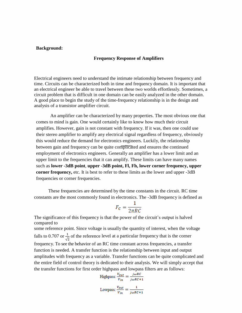
Background:
Frequency Response of Amplifiers
Electrical engineers need to understand the intimate relationship between frequency and
time. Circuits can be characterized both in time and frequency domain. It is important that
an electrical engineer be able to travel between these two worlds effortlessly. Sometimes, a
circuit problem that is difficult in one domain can be easily analyzed in the other domain.
A good place to begin the study of the time-frequency relationship is in the design and
analysis of a transistor amplifier circuit.
An amplifier can be characterized by many properties. The most obvious one that
comes to mind is gain. One would certainly like to know how much their circuit
amplifies. However, gain is not constant with frequency. If it was, then one could use
their stereo amplifier to amplify any electrical signal regardless of frequency, obviously
this would reduce the demand for electronics engineers. Luckily, the relationship
between gain and frequency can be quite complicated and ensures the continued
employment of electronics engineers. Generally an amplifier has a lower limit and an
upper limit to the frequencies that it can amplify. These limits can have many names
such as lower -3dB point, upper -3dB point, Fl, Fh, lower corner frequency, upper
corner frequency, etc. It is best to refer to these limits as the lower and upper -3dB
frequencies or corner frequencies.
These frequencies are determined by the time constants in the circuit. RC time
constants are the most commonly found in electronics. The -3dB frequency is defined as
The significance of this frequency is that the power of the circuit’s output is halved
compared to
some reference point. Since voltage is usually the quantity of interest, when the voltage
falls to 0.707 or 1
√2 of the reference level at a particular frequency that is the corner
frequency. To see the behavior of an RC time constant across frequencies, a transfer
function is needed. A transfer function is the relationship between input and output
amplitudes with frequency as a variable. Transfer functions can be quite complicated and
the entire field of control theory is dedicated to their analysis. We will simply accept that
the transfer functions for first order highpass and lowpass filters are as follows:
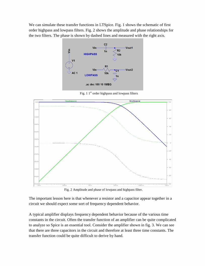
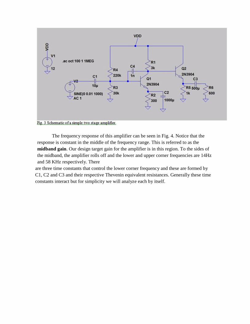
We can simulate these transfer functions in LTSpice. Fig. 1 shows the schematic of first
order highpass and lowpass filters. Fig. 2 shows the amplitude and phase relationships for
the two filters. The phase is shown by dashed lines and measured with the right axis.
Fig. 1 1st
order highpass and lowpass filters
Fig. 2 Amplitude and phase of lowpass and highpass filter.
The important lesson here is that whenever a resistor and a capacitor appear together in a
circuit we should expect some sort of frequency dependent behavior.
A typical amplifier displays frequency dependent behavior because of the various time
constants in the circuit. Often the transfer function of an amplifier can be quite complicated
to analyze so Spice is an essential tool. Consider the amplifier shown in fig. 3. We can see
that there are three capacitors in the circuit and therefore at least three time constants. The
transfer function could be quite difficult to derive by hand.
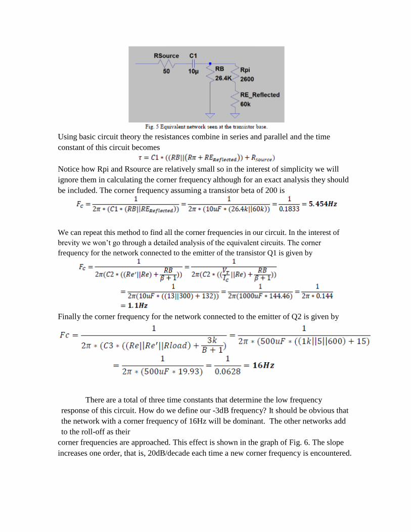
The frequency response of this amplifier can be seen in Fig. 4. Notice that the
response is constant in the middle of the frequency range. This is referred to as the
midband gain. Our design target gain for the amplifier is in this region. To the sides of
the midband, the amplifier rolls off and the lower and upper corner frequencies are 14Hz
and 58 KHz respectively. There
are three time constants that control the lower corner frequency and these are formed by
C1, C2 and C3 and their respective Thevenin equivalent resistances. Generally these time
constants interact but for simplicity we will analyze each by itself.
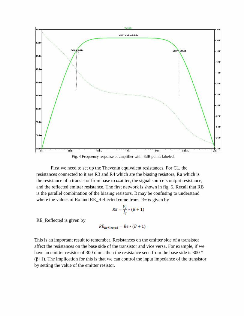
Fig. 4 Frequency response of amplifier with -3dB points labeled.
First we need to set up the Thevenin equivalent resistances. For C1, the
resistances connected to it are R3 and R4 which are the biasing resistors, Rπ which is
the resistance of a transistor from base to emitter, the signal source’s output resistance,
and the reflected emitter resistance. The first network is shown in fig. 5. Recall that RB
is the parallel combination of the biasing resistors. It may be confusing to understand
where the values of Rπ and RE_Reflected come from. Rπ is given by
RE_Reflected is given by
This is an important result to remember. Resistances on the emitter side of a transistor
affect the resistances on the base side of the transistor and vice versa. For example, if we
have an emitter resistor of 300 ohms then the resistance seen from the base side is 300 *
(β+1). The implication for this is that we can control the input impedance of the transistor
by setting the value of the emitter resistor.
Using basic circuit theory the resistances combine in series and parallel and the time
constant of this circuit becomes
Notice how Rpi and Rsource are relatively small so in the interest of simplicity we will
ignore them in calculating the corner frequency although for an exact analysis they should
be included. The corner frequency assuming a transistor beta of 200 is
We can repeat this method to find all the corner frequencies in our circuit. In the interest of
brevity we won’t go through a detailed analysis of the equivalent circuits. The corner
frequency for the network connected to the emitter of the transistor Q1 is given by
Finally the corner frequency for the network connected to the emitter of Q2 is given by
There are a total of three time constants that determine the low frequency
response of this circuit. How do we define our -3dB frequency? It should be obvious that
the network with a corner frequency of 16Hz will be dominant. The other networks add
to the roll-off as their
corner frequencies are approached. This effect is shown in the graph of Fig. 6. The slope
increases one order, that is, 20dB/decade each time a new corner frequency is encountered.
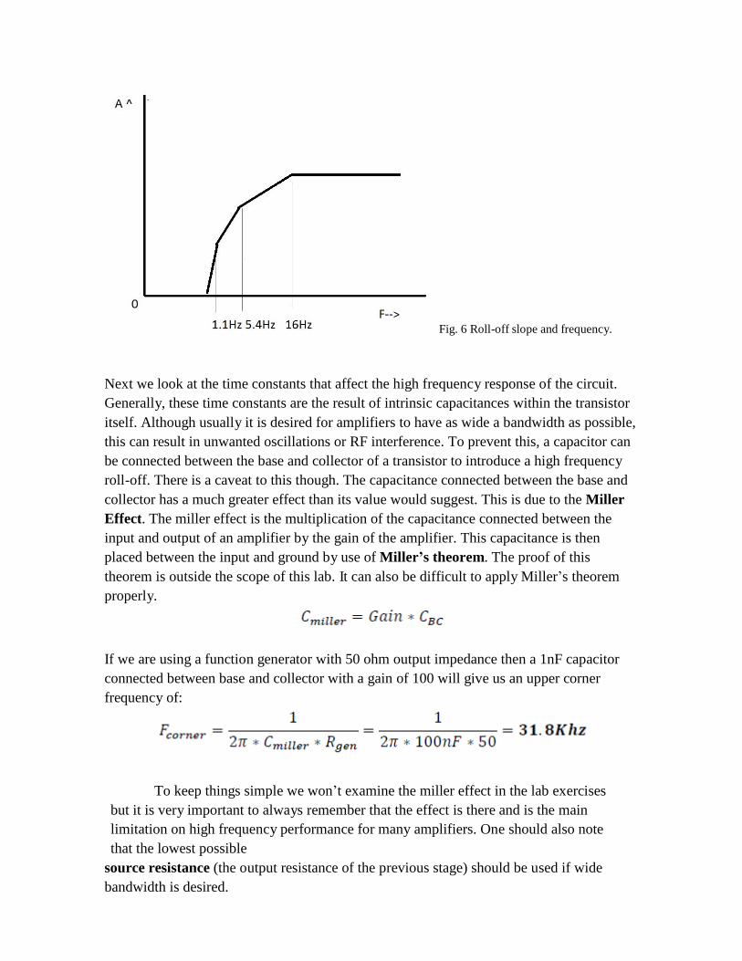
Fig. 6 Roll-off slope and frequency.
Next we look at the time constants that affect the high frequency response of the circuit.
Generally, these time constants are the result of intrinsic capacitances within the transistor
itself. Although usually it is desired for amplifiers to have as wide a bandwidth as possible,
this can result in unwanted oscillations or RF interference. To prevent this, a capacitor can
be connected between the base and collector of a transistor to introduce a high frequency
roll-off. There is a caveat to this though. The capacitance connected between the base and
collector has a much greater effect than its value would suggest. This is due to the Miller
Effect. The miller effect is the multiplication of the capacitance connected between the
input and output of an amplifier by the gain of the amplifier. This capacitance is then
placed between the input and ground by use of Miller’s theorem. The proof of this
theorem is outside the scope of this lab. It can also be difficult to apply Miller’s theorem
properly.
If we are using a function generator with 50 ohm output impedance then a 1nF capacitor
connected between base and collector with a gain of 100 will give us an upper corner
frequency of:
To keep things simple we won’t examine the miller effect in the lab exercises
but it is very important to always remember that the effect is there and is the main
limitation on high frequency performance for many amplifiers. One should also note
that the lowest possible
source resistance (the output resistance of the previous stage) should be used if wide
bandwidth is desired.
The Time-Frequency
Relationship
A mathematician will likely explain the relationship between time and frequency
through the use of Fourier transforms. While Fourier transforms are very useful and come
into play in more advanced electrical engineering courses, they don’t really help us in the
lab. It is possible to empirically determine how a circuit’s behavior changes with
frequency. The main motivation for this in the lab setting is that instruments which can
directly display results in frequency domain are usually very expensive. But luckily time
domain instruments like the common oscilloscope can give us insight into the frequency
domain behavior of a circuit.
The easiest way to measure the frequency response of an amplifier would be to
connect a sweep function generator to the input and a spectrum analyzer to the output.
This would instantly produce the frequency response. If one can’t afford a spectrum
analyzer they could vary the function generator themselves and note the amplitude of the
output on an oscilloscope to create a frequency response plot. The disadvantages to this
are tedium and possible limitations of the function generator. What if the amplifier’s
bandwidth exceeded that of the function generator? Luckily there is a better way to
quickly test the frequency response of an amplifier.
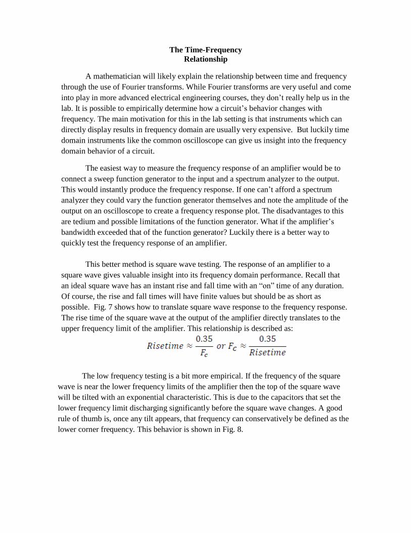
This better method is square wave testing. The response of an amplifier to a
square wave gives valuable insight into its frequency domain performance. Recall that
an ideal square wave has an instant rise and fall time with an “on” time of any duration.
Of course, the rise and fall times will have finite values but should be as short as
possible. Fig. 7 shows how to translate square wave response to the frequency response.
The rise time of the square wave at the output of the amplifier directly translates to the
upper frequency limit of the amplifier. This relationship is described as:
The low frequency testing is a bit more empirical. If the frequency of the square
wave is near the lower frequency limits of the amplifier then the top of the square wave
will be tilted with an exponential characteristic. This is due to the capacitors that set the
lower frequency limit discharging significantly before the square wave changes. A good
rule of thumb is, once any tilt appears, that frequency can conservatively be defined as the
lower corner frequency. This behavior is shown in Fig. 8.
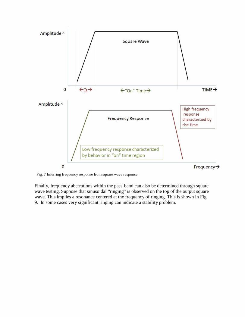
Fig. 7 Inferring frequency response from square wave response.
Finally, frequency aberrations within the pass-band can also be determined through square
wave testing. Suppose that sinusoidal “ringing” is observed on the top of the output square
wave. This implies a resonance centered at the frequency of ringing. This is shown in Fig.
9. In some cases very significant ringing can indicate a stability problem.
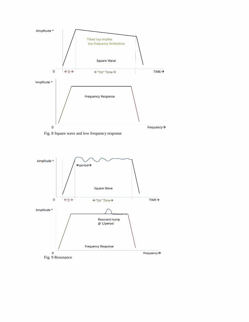
Fig. 8 Square wave and low frequency response
Fig. 9 Resonance
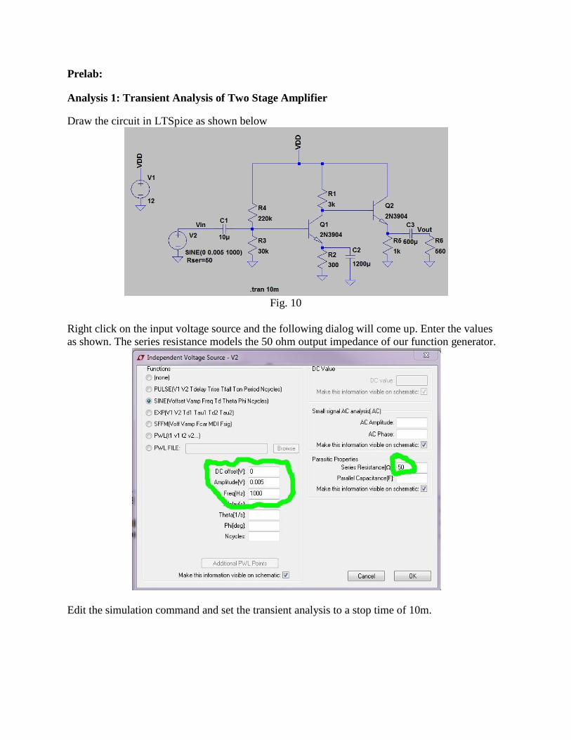
Prelab: Analysis 1: Transient Analysis of Two Stage Amplifier
Draw the circuit in LTSpice as shown below
Fig. 10
Right click on the input voltage source and the following dialog will come up. Enter the values
as shown. The series resistance models the 50 ohm output impedance of our function generator.
Edit the simulation command and set the transient analysis to a stop time of 10m.
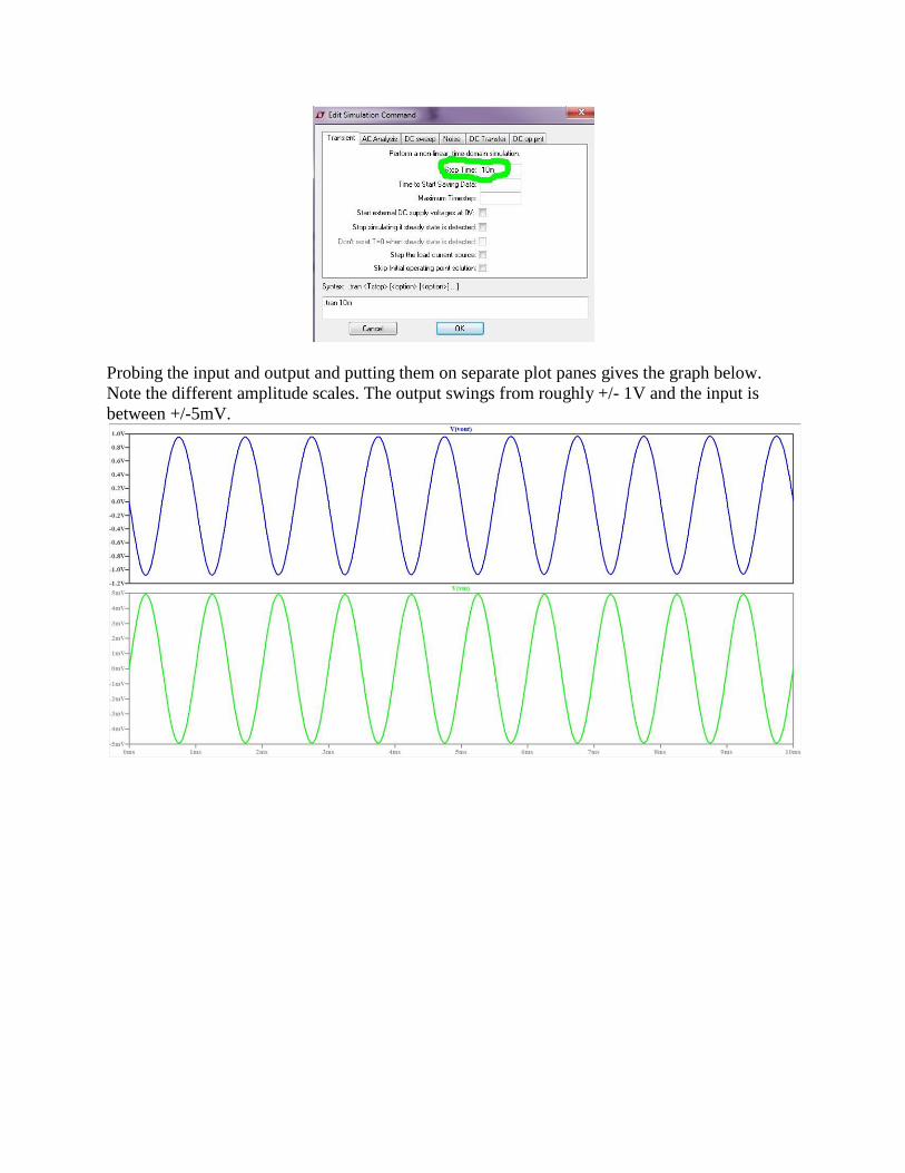
Probing the input and output and putting them on separate plot panes gives the graph below.
Note the different amplitude scales. The output swings from roughly +/- 1V and the input is
between +/-5mV.
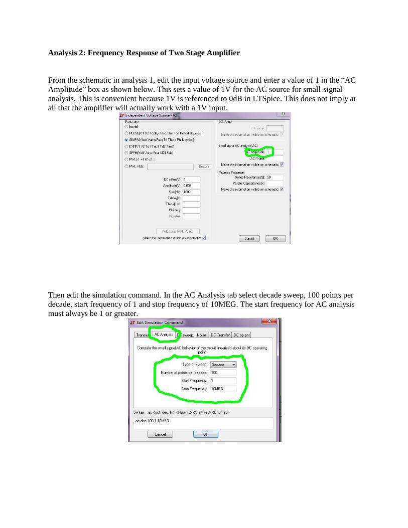
Analysis 2: Frequency Response of Two Stage Amplifier
From the schematic in analysis 1, edit the input voltage source and enter a value of 1 in the “AC
Amplitude” box as shown below. This sets a value of 1V for the AC source for small-signal
analysis. This is convenient because 1V is referenced to 0dB in LTSpice. This does not imply at
all that the amplifier will actually work with a 1V input.
Then edit the simulation command. In the AC Analysis tab select decade sweep, 100 points per
decade, start frequency of 1 and stop frequency of 10MEG. The start frequency for AC analysis
must always be 1 or greater.
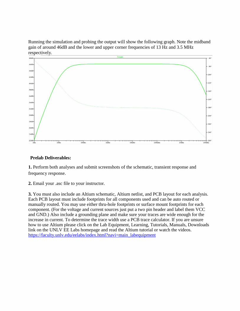
Running the simulation and probing the output will show the following graph. Note the midband
gain of around 46dB and the lower and upper corner frequencies of 13 Hz and 3.5 MHz
respectively.
Prelab Deliverables:
1. Perform both analyses and submit screenshots of the schematic, transient response and
frequency response.
2. Email your .asc file to your instructor.
3. You must also include an Altium schematic, Altium netlist, and PCB layout for each analysis. Each PCB layout must include footprints for all components used and can be auto routed or manually routed. You may use either thru-hole footprints or surface mount footprints for each component. (For the voltage and current sources just put a two pin header and label them VCC and GND.) Also include a grounding plane and make sure your traces are wide enough for the increase in current. To determine the trace width use a PCB trace calculator. If you are unsure how to use Altium please click on the Lab Equipment, Learning, Tutorials, Manuals, Downloads link on the UNLV EE Labs homepage and read the Altium tutorial or watch the videos. https://faculty.unlv.edu/eelabs/index.html?navi=main_labequipment
Lab Experiments:
Experiment 1: Rise Time of Function Generator
We must first characterize our test equipment and verify we can use them for our lab.
Directly connect the function generator to the oscilloscope. Ideally this should be done with a
coaxial cable but if not available in the lab the crude scope probe to function generator probe
method can be used. Set the function generator to 1V amplitude and 10 KHz square wave. Zoom
in on the rising edge of the square wave and measure the time it takes for the output to rise from
10% to 90% of the final amplitude of the square wave. This is the rise time. Note this
measurement. Some scopes will calculate this automatically for you, but a visual inspection is a
good idea
Experiment 2: Two Stage Transistor Amplifier
Circuit Description:
We will be constructing the circuit simulated in the prelab. Some background will help us
understand the circuit. This circuit is a two stage amplifier consisting of a common emitter stage
and an emitter follower (common collector stage). The load resistor approximates a 600 ohm
load which is a common value for high quality headphones. It is also historically important
impedance for telephone circuits just as 50 ohm loads are for RF. The emitter follower’s emitter
resistance is higher than the load resistance. This will limit the output voltage swing into the load
because the circuit will be current limited by this resistor. This was done intentionally to
illustrate that the output impedance of an emitter follower is not the emitter resistor. The
performance of the amplifier can be improved by reducing the emitter resistor. The collector of
Q1 is at 6V set by the biasing circuit. For the sake of completeness we will go through the
biasing procedure followed to arrive at the bias circuit.
1. Decide on a collector current (2mA in this example).
2. Decide on what we want the collector voltage to be (6V in this example)
3. Pick a collector resistor based on the collector current and collector voltage
(6V/2mA=3k).
4. Decide on a nominal DC gain (Gain=Rc/Re, gain chosen to be 10=3k/300).
5. Estimate base current (assumed beta to be 200, 2mA/200=10uA)
6. Calculate emitter voltage (Ie*Re=2mA*300=0.6V)
7. Add forward bias diode drop to emitter voltage to get base voltage (Vbe+0.6V=1.3V)
8. Design voltage divider that sets base voltage to 1.3V and allows 5*base current to
flow).
Experiment 2 Procedure: 1. Build circuit as simulated in the prelab.
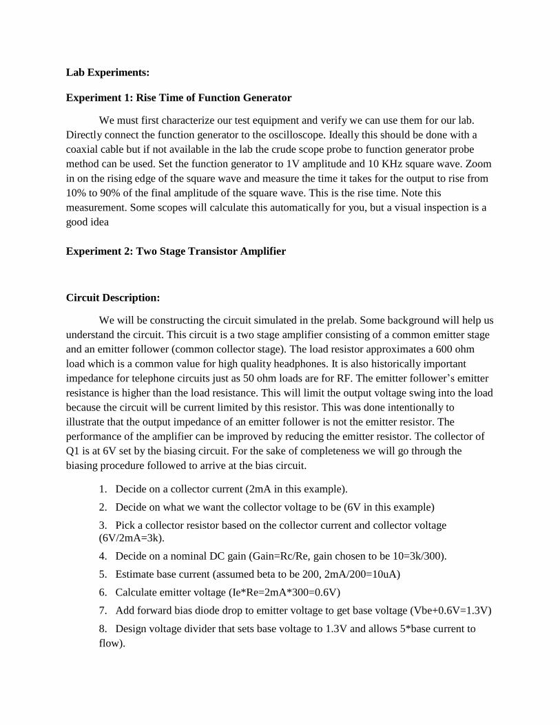
2. Apply a 10mV 1 KHz signal to the input and look at the output of the amplifier on an oscilloscope.
Note the amplitude of the output signal and calculate the gain of the amplifier. This will be our
midband gain. Take a picture of the scope screen.
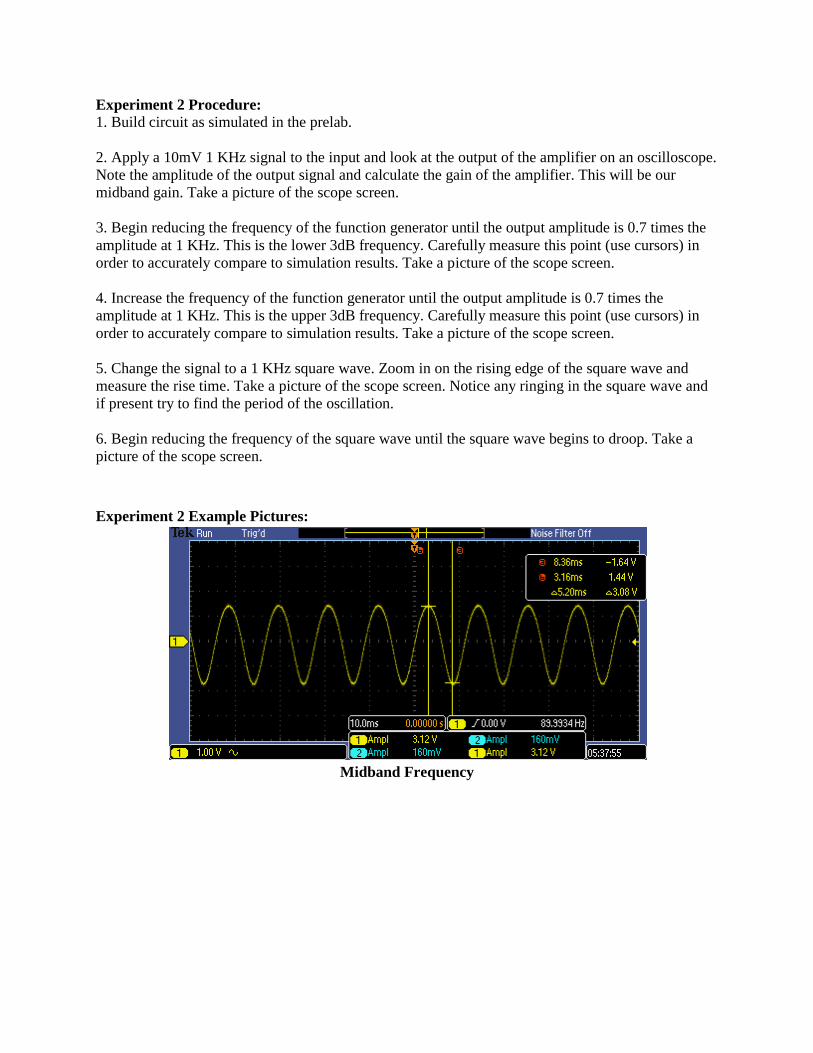
3. Begin reducing the frequency of the function generator until the output amplitude is 0.7 times the
amplitude at 1 KHz. This is the lower 3dB frequency. Carefully measure this point (use cursors) in
order to accurately compare to simulation results. Take a picture of the scope screen.
4. Increase the frequency of the function generator until the output amplitude is 0.7 times the
amplitude at 1 KHz. This is the upper 3dB frequency. Carefully measure this point (use cursors) in
order to accurately compare to simulation results. Take a picture of the scope screen.
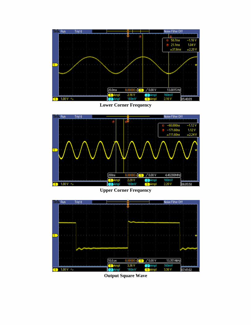
5. Change the signal to a 1 KHz square wave. Zoom in on the rising edge of the square wave and
measure the rise time. Take a picture of the scope screen. Notice any ringing in the square wave and
if present try to find the period of the oscillation.
6. Begin reducing the frequency of the square wave until the square wave begins to droop. Take a
picture of the scope screen.
Experiment 2 Example Pictures:
Midband Frequency
Lower Corner Frequency
Upper Corner Frequency
Output Square Wave
Rise Time Measurement
Droopy Square Wave.
Postlab Deliverables
1. All indicated scope screenshots.
Questions:
1. What was the midband gain of your circuit and how does this compare to your simulation
results? Remember gain in dB is:
2. What were your upper and lower corner frequencies? How do these compare to your
simulation results?
3. Was there any ringing in your square wave response? If so what frequency was the ringing
at?
4. Speculate as to why you had ringing in your measured results yet not in your simulations? (If
you didn’t have ringing, still speculate what could cause it.)
5. Based on your answers to 2 and 3 sketch a frequency response graph by hand.
6. Regarding results from experiment 1, does the measured rise time of the function generator
affect the accuracy of our results?
7. Write a few sentences about the guy after whom the Miller effect is named.