Embed Size (px)
Citation preview
EE610: CMOS AnalogEE610: CMOS Analog Circuits
L3: MOS Models-3 (5th Aug. 2013)
B. MazhariDept of EE IIT Kanpur
G-NumberB. Mazhari, IITK76
Dept. of EE, IIT Kanpur

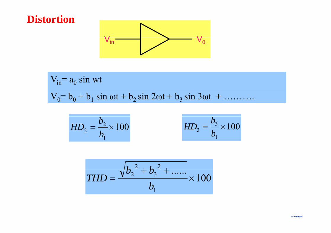
Why does sound quality of my audio system degradeat high volume?g
G-NumberB. Mazhari, IITK77
V V
Distortion
Vin V0
Vin= a0 sin wt
V0= b0 + b1 sin ωt + b2 sin 2ωt + b3 sin 3ωt + ……….
1001
22
bbHD 100
1
33
bb
HD
22 bb100
......
1
32
bbb
THD
G-NumberB. Mazhari, IITK78
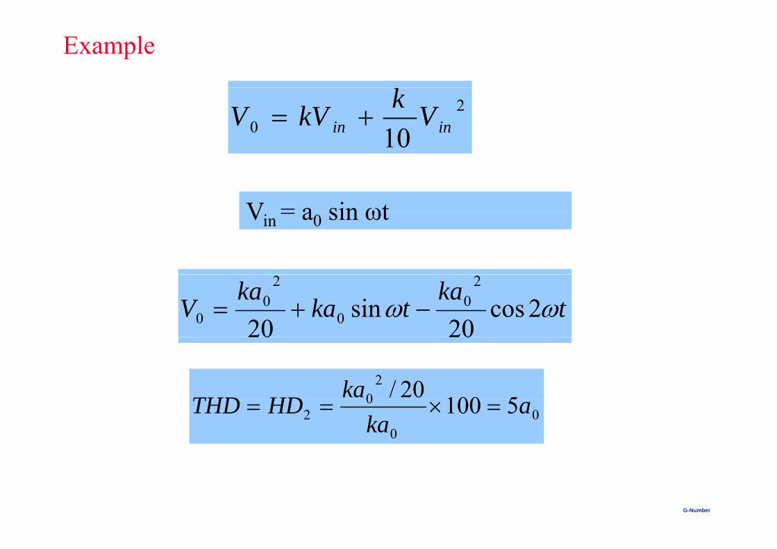
Example
20 10 inin VkkVV
V = a sin ωtVin = a0 sin ωt
tka
tkaka
V 2cos20
sin20
20
0
20
0 2020
20 5100
20/kaHDTHD 0
0
02 5100 a
kaHDTHD
G-NumberB. Mazhari, IITK79

How do we measure the speed of a transistor?
G-NumberB. Mazhari, IITK80
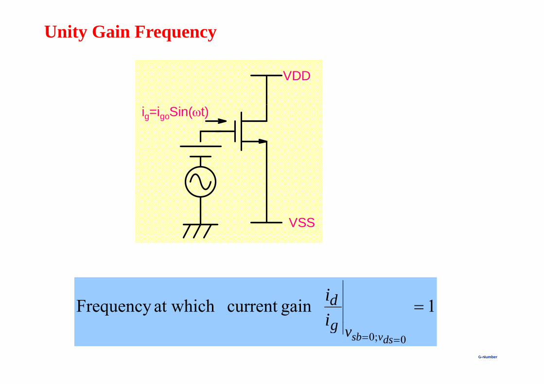
Unity Gain Frequency
VDD
ig=igoSin(t)
VSS
1gain current at which Frequency dii
G-NumberB. Mazhari, IITK81
0;0 dsvsbvgi
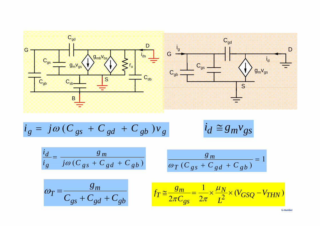
C Cgd
Gig
id
D
Cgd
Gids
Cgsgmbvbs
D
CgsCgb
S
gmvgs
dgmvgs
Cdb
roCgs
Cgb CsbS
S
B
ggbgdgsg vCCCji )( d m gsi g v
( )d mg gs gd gb
i gi j C C C
1
( )mg
C C C
mg 1 ( )m Ngf V V
( )g gs gd gbi j C C C ( )T gs gd gbC C C
G-NumberB. Mazhari, IITK82
gbgdgs
mT CCC
2 ( )2 2
m NT GSQ THN
gs
gf V VC L
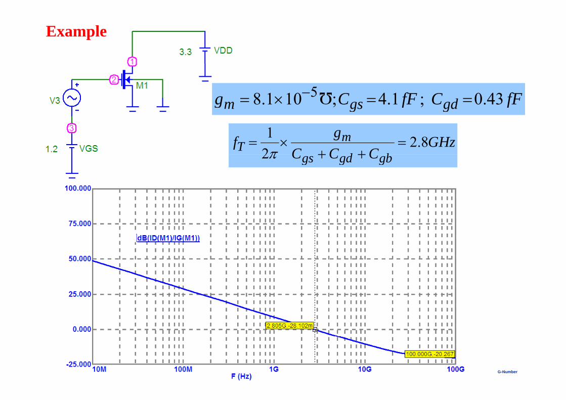
Example
58.1 10 ; 4.1 ; 0.43m gs gdg C fF C fF g g
1 2.82
mT
d b
gf GHzC C C
2 gs gd gbC C C
G-NumberB. Mazhari, IITK83
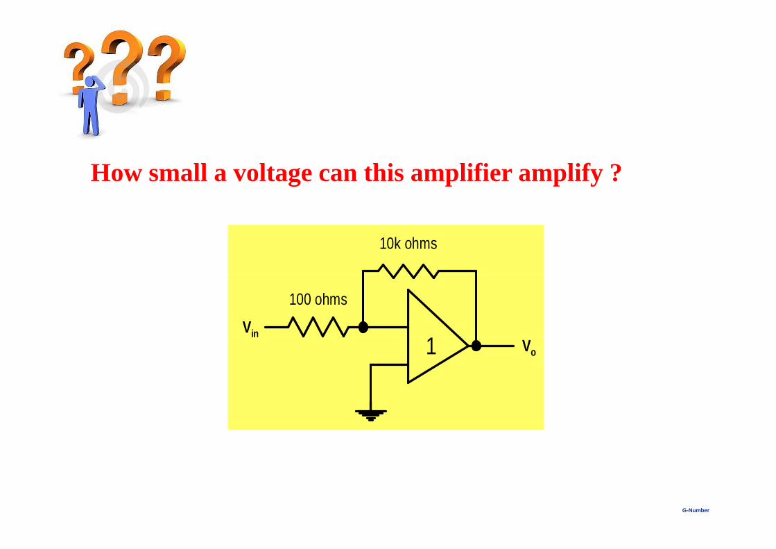
How small a voltage can this amplifier amplify ?
10k ohms
1
100 ohms
Vin1 Vo
in
G-NumberB. Mazhari, IITK84
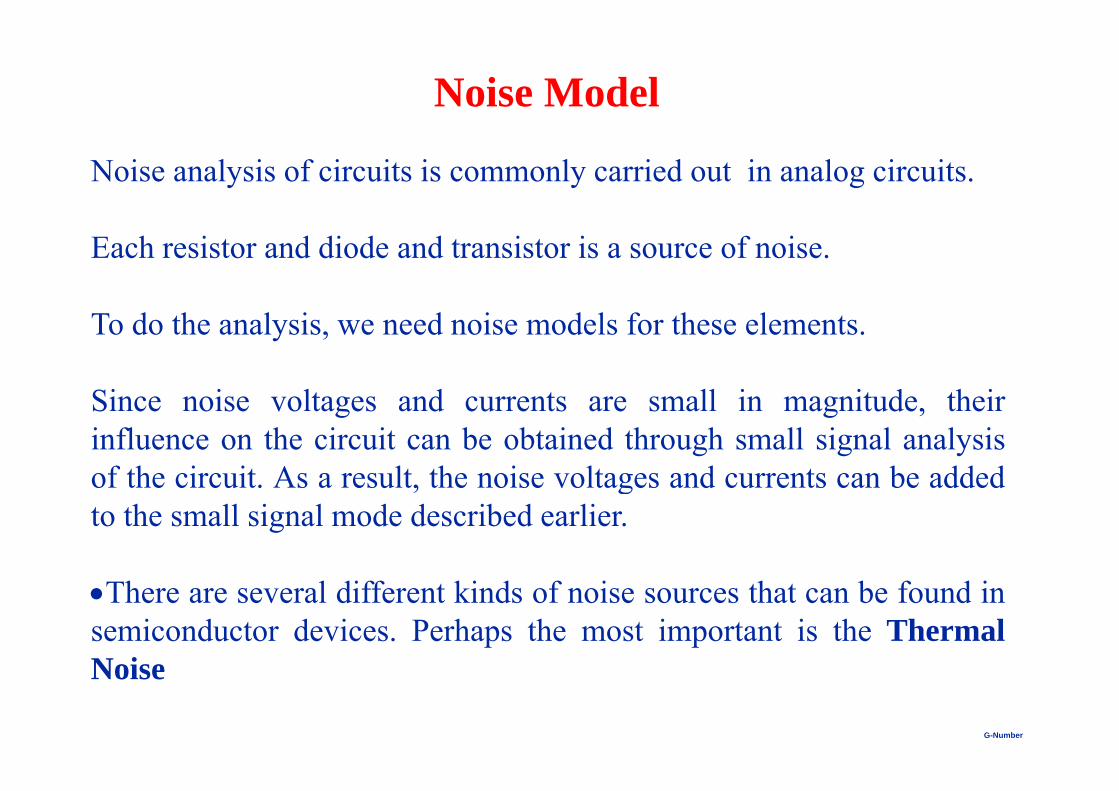
Noise Model
Noise analysis of circuits is commonly carried out in analog circuits.
Each resistor and diode and transistor is a source of noise.
To do the analysis, we need noise models for these elements.
Si i lt d t ll i it d th iSince noise voltages and currents are small in magnitude, theirinfluence on the circuit can be obtained through small signal analysisof the circuit. As a result, the noise voltages and currents can be addedof the circuit. As a result, the noise voltages and currents can be addedto the small signal mode described earlier.
There are several different kinds of noise sources that can be found insemiconductor devices. Perhaps the most important is the ThermalNoise
G-NumberB. Mazhari, IITK85
Noise
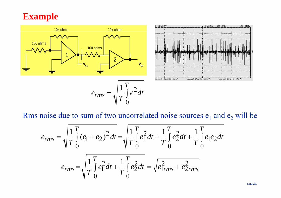
10k ohms 10k ohms
Example
1100 ohms
100 ohms
12
Vo1 Vo2
21 Trmse e dt
T
0T
Rms noise due to sum of two uncorrelated noise sources e1 and e2 will be
2 2 21 2 1 2 1 2
0 0 0 0
1 1 1 1( )T T T T
rmse e e dt e dt e dt e e dtT T T T
0 0 0 0T T T T
2 2 2 21 1T Te e dt e dt e e
G-NumberB. Mazhari, IITK86
1 2 1 20 0
rms rms rmse e dt e dt e eT T
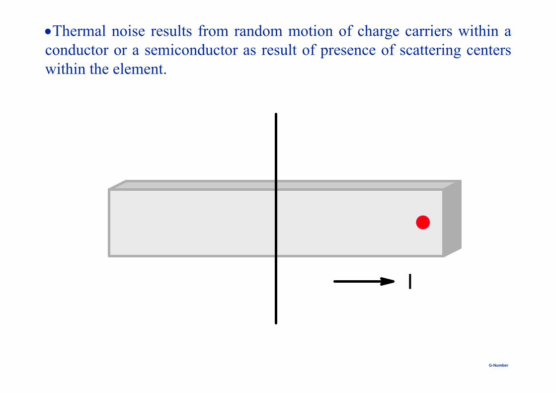
Thermal noise results from random motion of charge carriers within aconductor or a semiconductor as result of presence of scattering centerswithin the element.
II
G-NumberB. Mazhari, IITK87
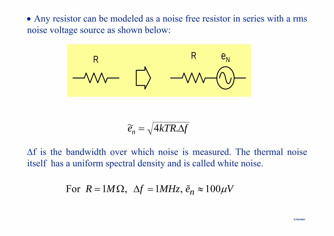
Any resistor can be modeled as a noise free resistor in series with a rmsnoise voltage source as shown below:
R eNR
fkTRen .4~
f is the bandwidth over which noise is measured. The thermal noiseitself has a uniform spectral density and is called white noise.
For 1 , 1 , 100nR M f MHz e V
G-NumberB. Mazhari, IITK88
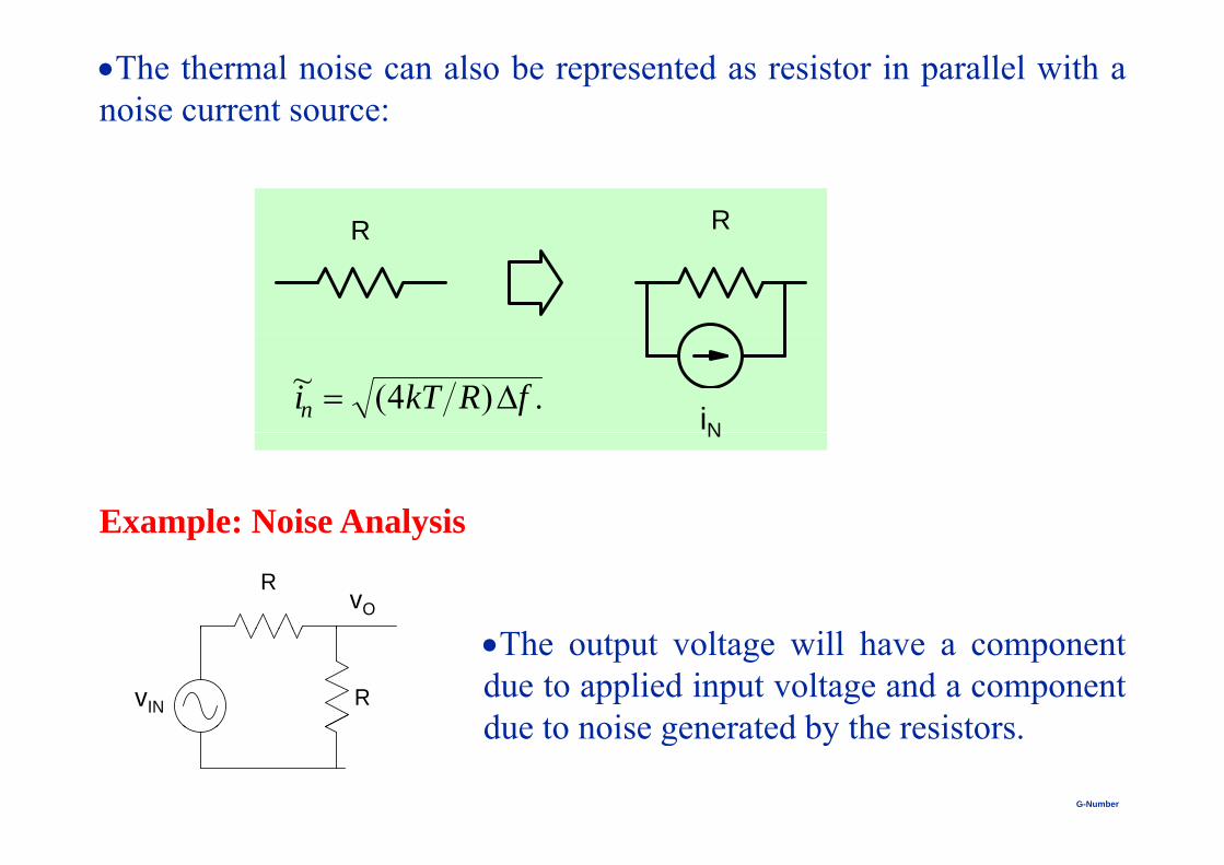
The thermal noise can also be represented as resistor in parallel with anoise current source:
R RR
iN.)4(~ fRkTin
N
Example: Noise AnalysisExample: Noise AnalysisR
vO
RvIN
The output voltage will have a componentdue to applied input voltage and a componentdue to noise generated by the resistors
G-NumberB. Mazhari, IITK89
due to noise generated by the resistors.
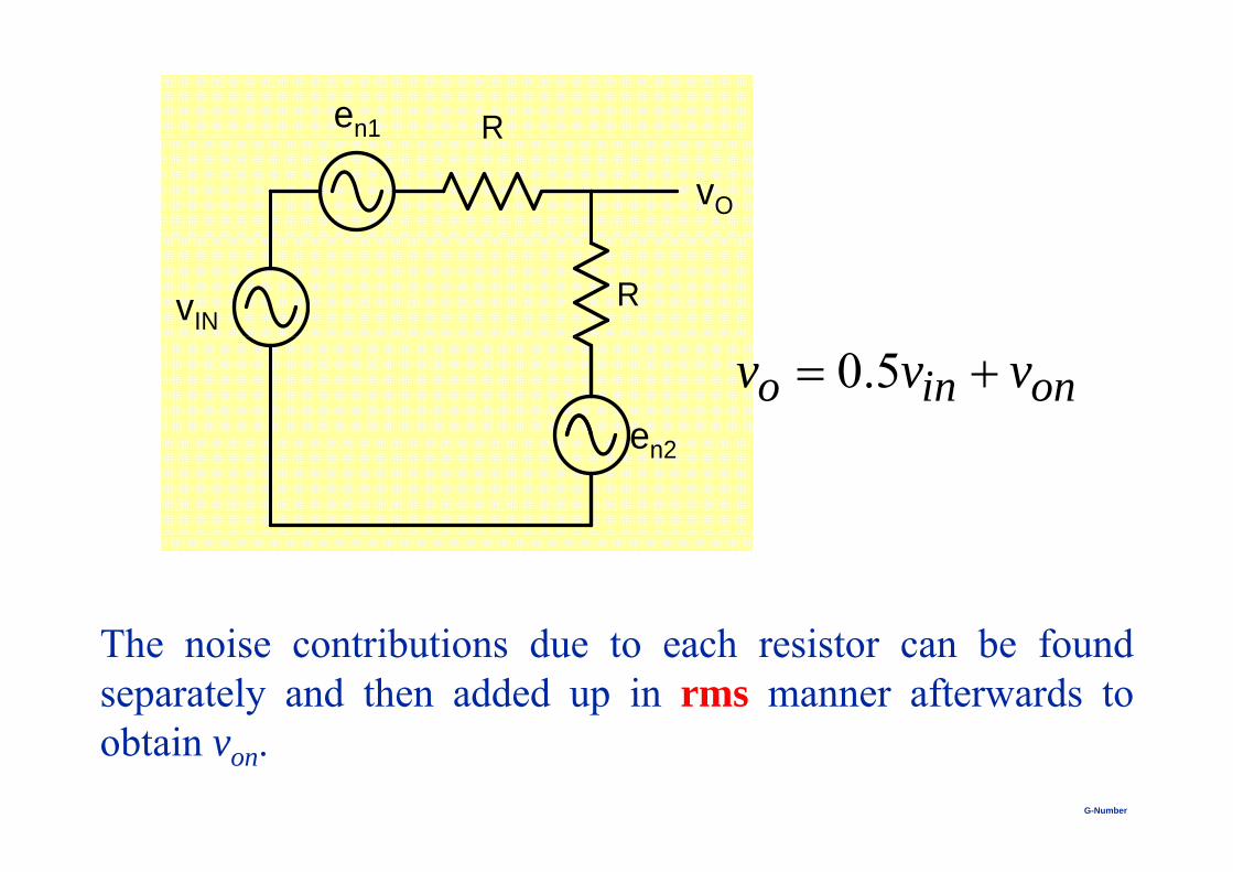
Ren1
vO
RvIN
e0.5o in onv v v
en2
Th i t ib ti d t h i t b f dThe noise contributions due to each resistor can be foundseparately and then added up in rms manner afterwards to
bt iG-NumberB. Mazhari, IITK
90
obtain von.
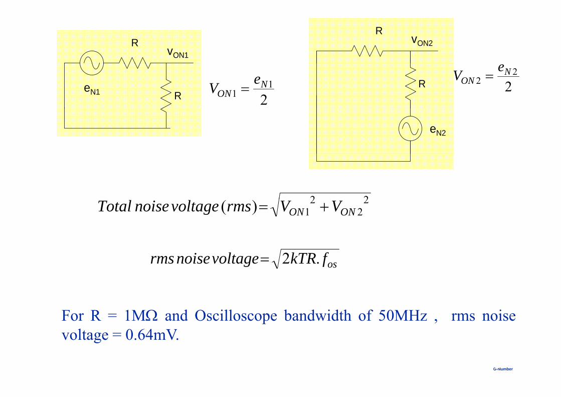
RvON1
RvON2
ReN1
21
1N
ONeV R 2
22
NON
eV
eN2
22 22
21)( ONON VVrmsvoltagenoiseTotal
osfkTRvoltagenoiserms .2
For R = 1M and Oscilloscope bandwidth of 50MHz , rms noisevoltage = 0 64mV
G-NumberB. Mazhari, IITK91
voltage = 0.64mV.
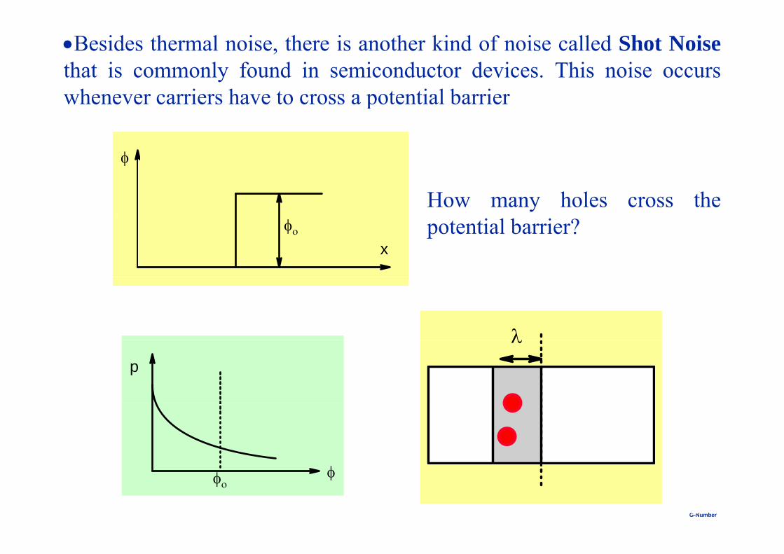
Besides thermal noise, there is another kind of noise called Shot Noisethat is commonly found in semiconductor devices. This noise occurswhenever carriers have to cross a potential barrier
How many holes cross the
x potential barrier?
p
G-NumberB. Mazhari, IITK92
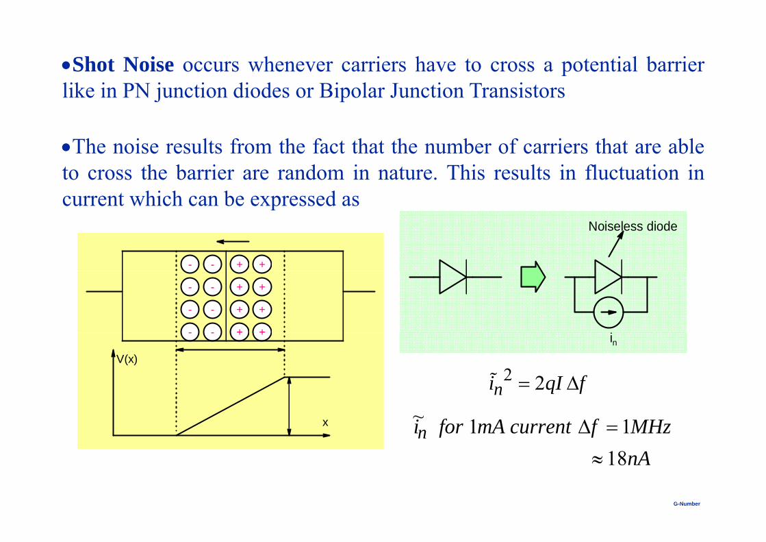
Shot Noise occurs whenever carriers have to cross a potential barrierlik i PN j ti di d Bi l J ti T i tlike in PN junction diodes or Bipolar Junction Transistors
The noise results from the fact that the number of carriers that are ableThe noise results from the fact that the number of carriers that are ableto cross the barrier are random in nature. This results in fluctuation incurrent which can be expressed asp
- + +-
Noiseless diode
-
-
- +
+
+
+
+
+-
-
-
2 2ni qI f
- + +-
V(x)
in
n
AMHzfcurrentmAforin
1811~ x
G-NumberB. Mazhari, IITK93
nA18
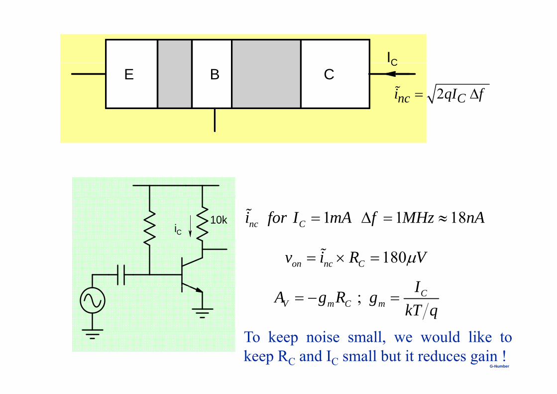
ICE B C
C
2nc Ci qI f
10kiC
1 1 18nc Ci for I mA f MHz nA
180on nc Cv i R V
I; CV m C m
IA g R gkT q
k i ll ld likG-NumberB. Mazhari, IITK
94
To keep noise small, we would like tokeep RC and IC small but it reduces gain !
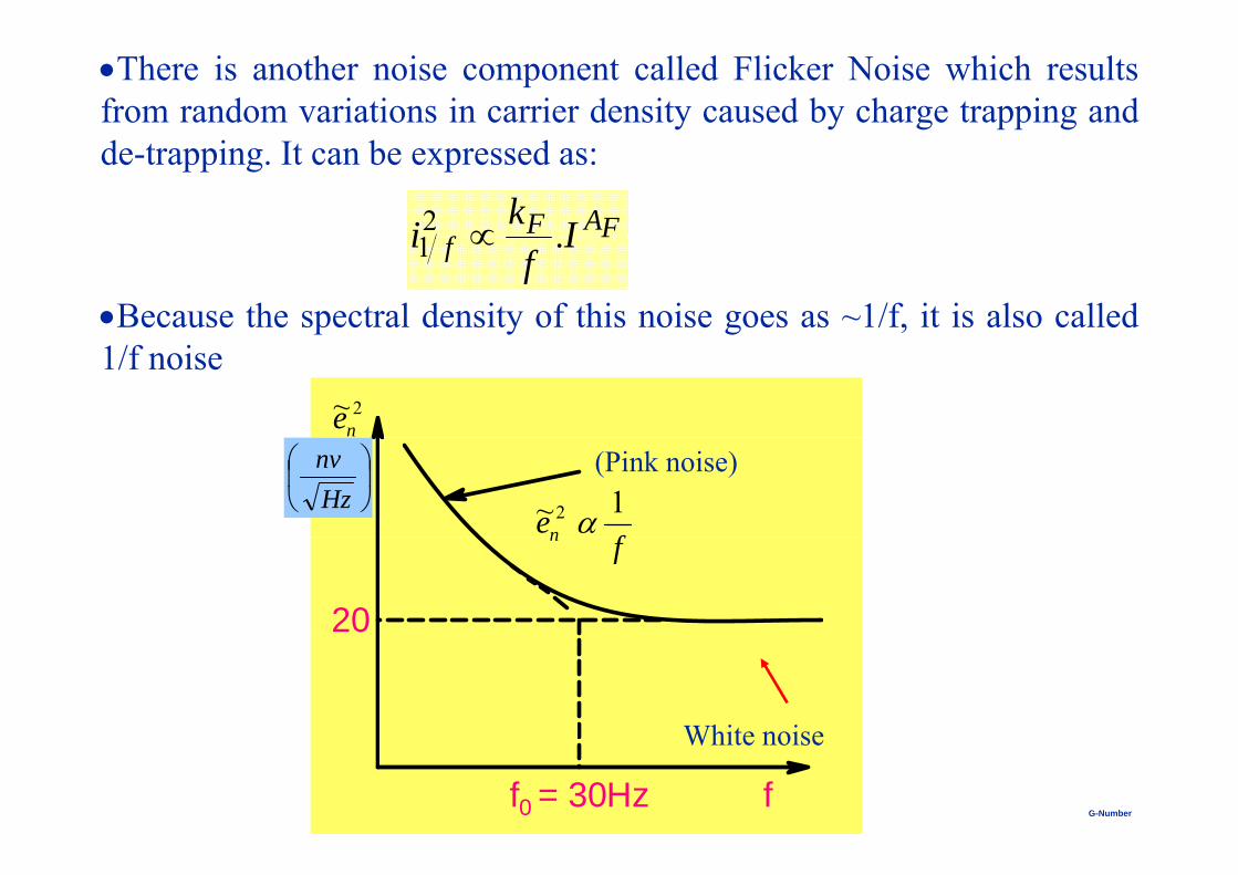
There is another noise component called Flicker Noise which resultsfrom random variations in carrier density caused by charge trapping andde-trapping. It can be expressed as:
FAFf Iki2
1 f If
i .1
Because the spectral density of this noise goes as ~1/f, it is also called1/f noise
2~ne
fen
1~2
Hznv (Pink noise)
20
fn
White noise
G-NumberB. Mazhari, IITK95ff0 = 30Hz
White noise
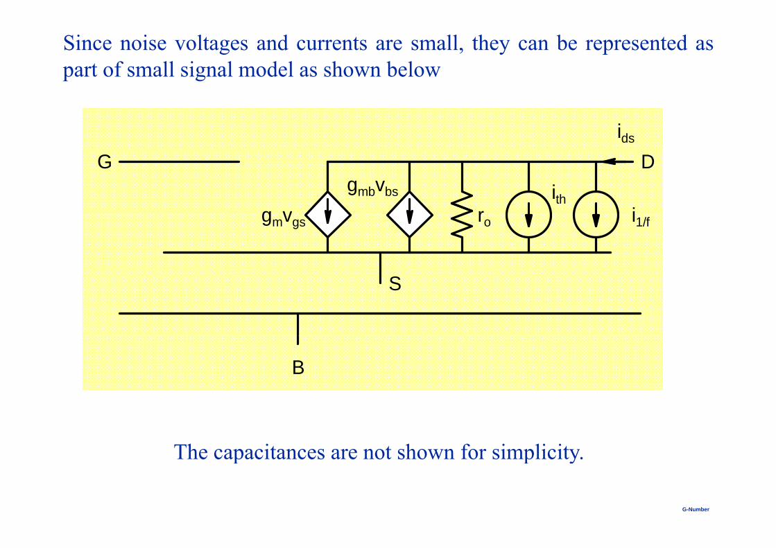
Since noise voltages and currents are small, they can be represented aspart of small signal model as shown below
ids
g v r
G D
iithgmbvbs
gmvgs ro i1/f
S
B
The capacitances are not shown for simplicity.
G-NumberB. Mazhari, IITK96
p p y
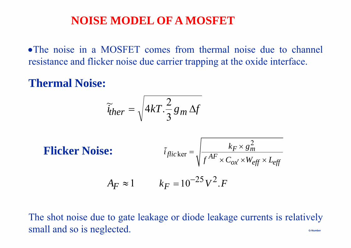
NOISE MODEL OF A MOSFET
The noise in a MOSFET comes from thermal noise due to channelresistance and flicker noise due carrier trapping at the oxide interface.
Thermal Noise:
fgkTi mther 32.4~
Flicker Noise:2
kF m
flik gi
Flicker Noise: kerflic AFox eff eff
if C W L
1A 25 210k V F1FA 25 210 .Fk V F
G-NumberB. Mazhari, IITK97
The shot noise due to gate leakage or diode leakage currents is relativelysmall and so is neglected.
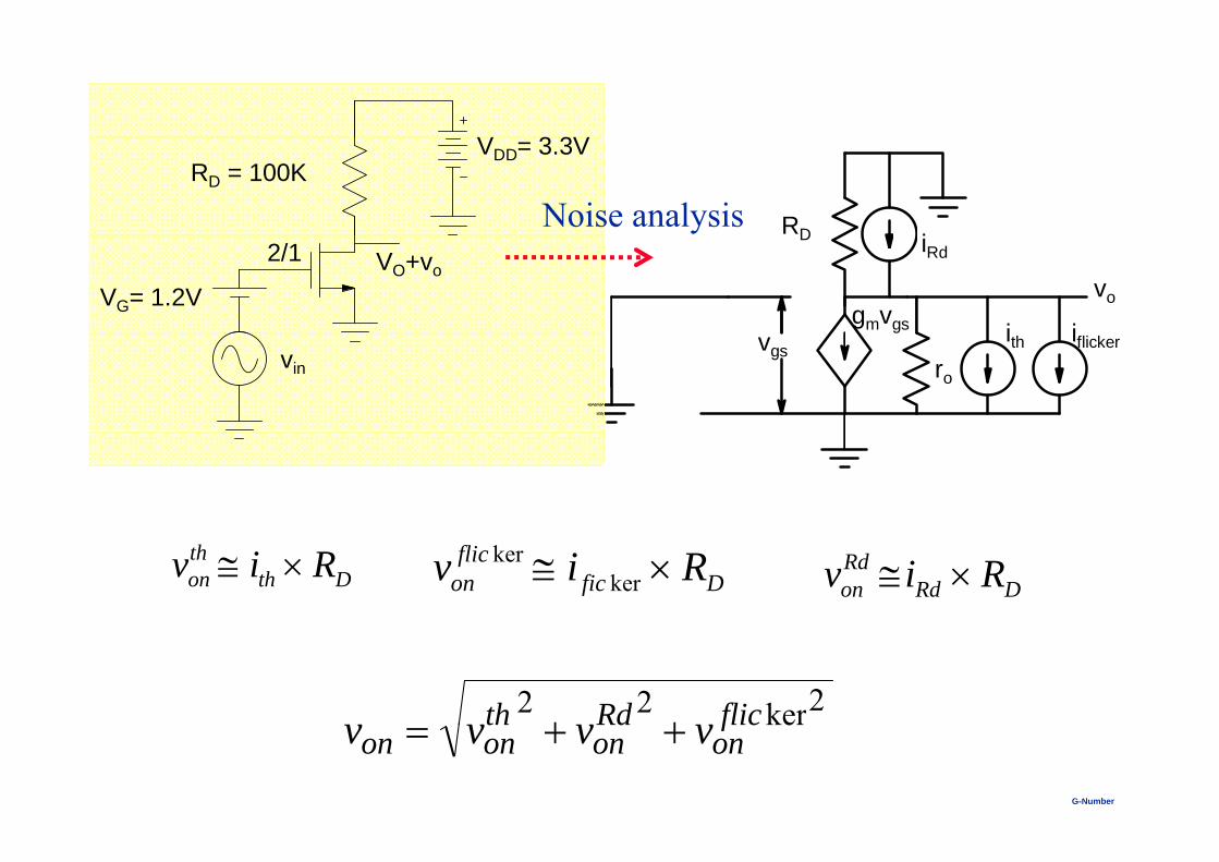
V 3 3V
RD i
VDD= 3.3VRD = 100K
Noise analysisD iRd
i i
vogmvgs
VG= 1.2V
2/1 VO+vo
vgsro
ith iflickervin
thon th Dv i R ker
kerflic
on fic Dv i R Rdon Rd Dv i R
2ker22 flicRdth G-NumberB. Mazhari, IITK
98
kerflicon
Rdon
thonon vvvv
V = 3 3V
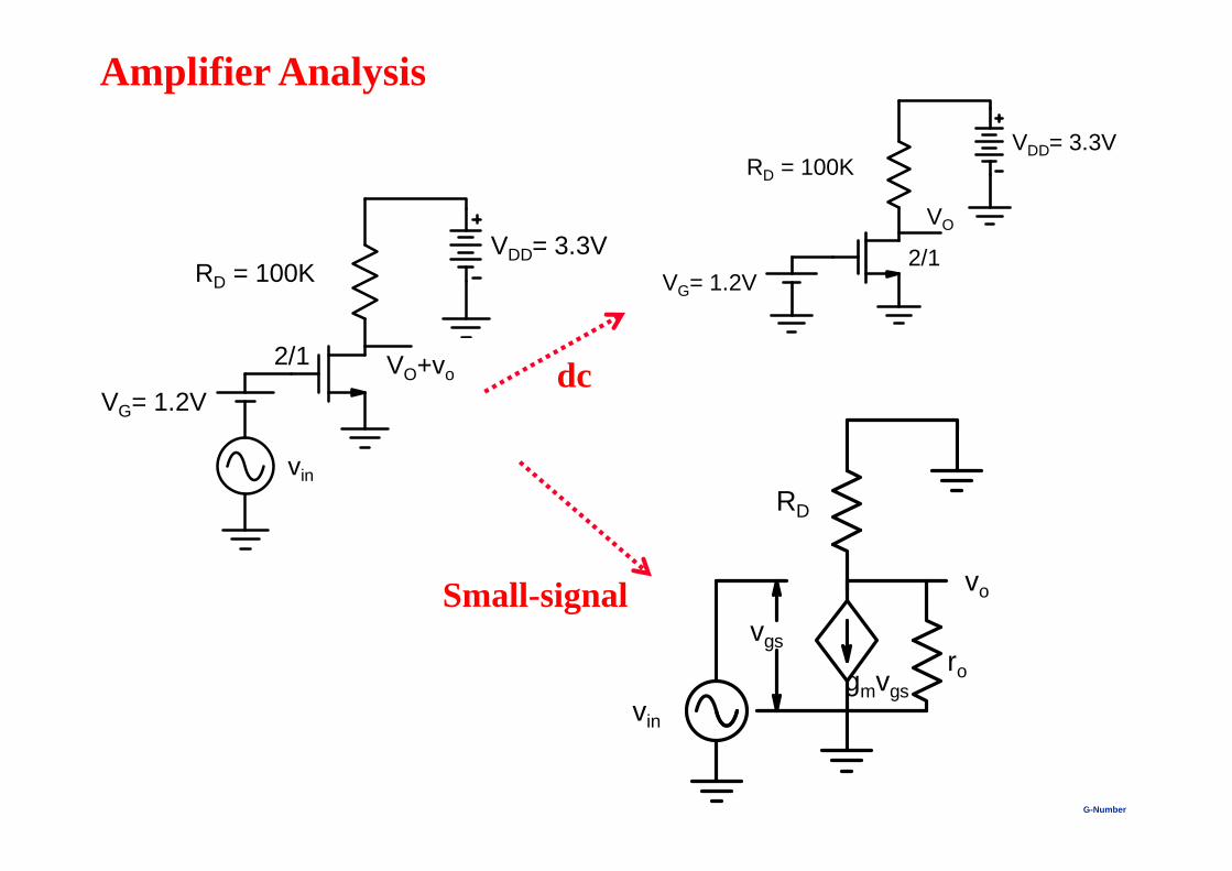
Amplifier Analysis
V 3 3V
VDD= 3.3VRD = 100K
VOVDD= 3.3V
RD = 100K VG= 1.2V2/1
VG= 1.2V
2/1 VO+vo dc
vin
RD
vo
vSmall-signal
ro
vin
vgs
gmvgs
G-NumberB. Mazhari, IITK99
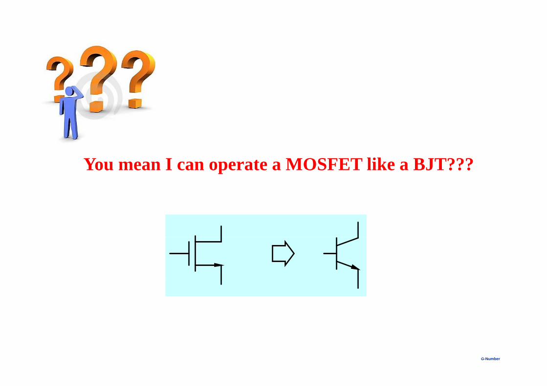
You mean I can operate a MOSFET like a BJT???
G-NumberB. Mazhari, IITK100
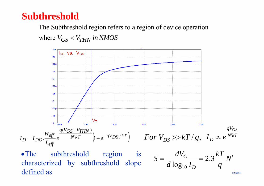
SubthresholdThe Subthreshold region refers to a region of device operation g g pwhere GS THNV V in NMOS
kTDSVqkTNTHNVGSVq
effW )(
/kTVF kTNqVGS
I kTDSVqkTNeff
effDOD ee
LW
II 1. ,/ qkTVFor DS kTND eI
The subthreshold region is NkTdVS G 32G-NumberB. Mazhari, IITK
101
e subt es o d eg o scharacterized by subthreshold slopedefined as
NqId
SD
G 3.2log10
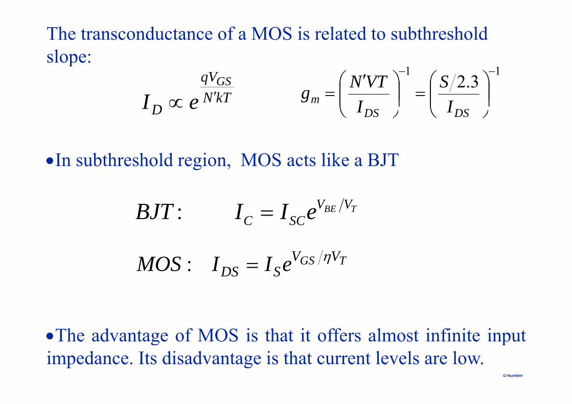
The transconductance of a MOS is related to subthreshold slope:p
113.2
DSDSm I
SIVTNgkTN
qV
D
GS
eI DSDS II
I bth h ld i MOS t lik BJT
D
In subthreshold region, MOS acts like a BJT
V V: BE TV VC SCBJT I I e
TGS VVSDS eIIMOS :
The advantage of MOS is that it offers almost infinite input
G-NumberB. Mazhari, IITK102
The advantage of MOS is that it offers almost infinite inputimpedance. Its disadvantage is that current levels are low.
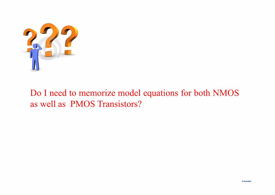
Do I need to memorize model equations for both NMOSqas well as PMOS Transistors?
G-NumberB. Mazhari, IITK103
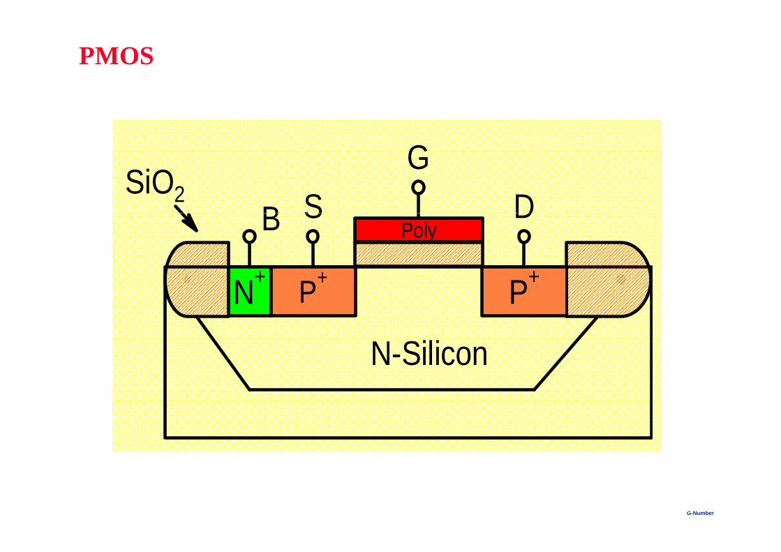
PMOS
GD
G
BSiO2 S
Poly
++ +
DB S
P+N+ P+
N-Silicon
G-NumberB. Mazhari, IITK104
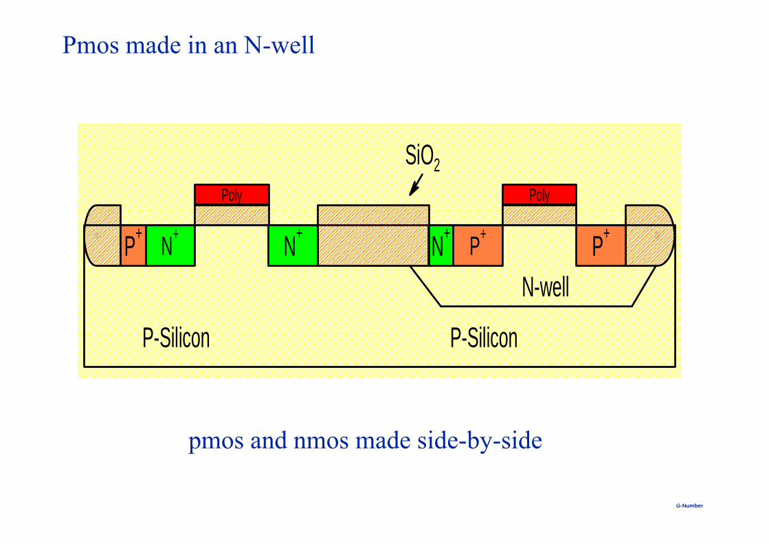
Pmos made in an N-well
SiOPoly Poly
SiO2
N+ N+P+ P+ P+N+
P Silicon P Silicon
N-well
P-Silicon P-Silicon
pmos and nmos made side-by-side
G-NumberB. Mazhari, IITK105
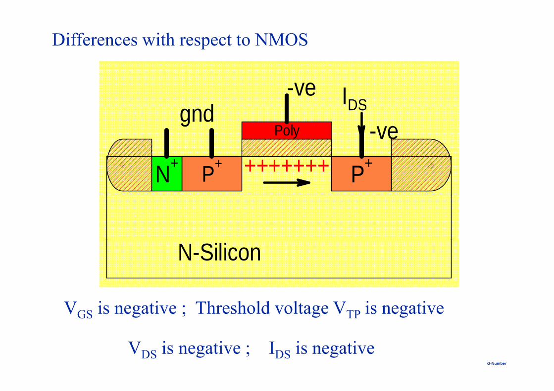
Differences with respect to NMOS
-ved
IDSPoly
gnd-ve
DS
P+ P+N+ +++++++
N-Silicon
VGS is negative ; Threshold voltage VTP is negative
G-NumberB. Mazhari, IITK106
VDS is negative ; IDS is negative
D D -
+
G G
+
-
++
SS
+- -
S ++
G -
SDPDSN II
D-
SGPGSN VV SDPDSN VV
G-NumberB. Mazhari, IITK107
SDPDSN
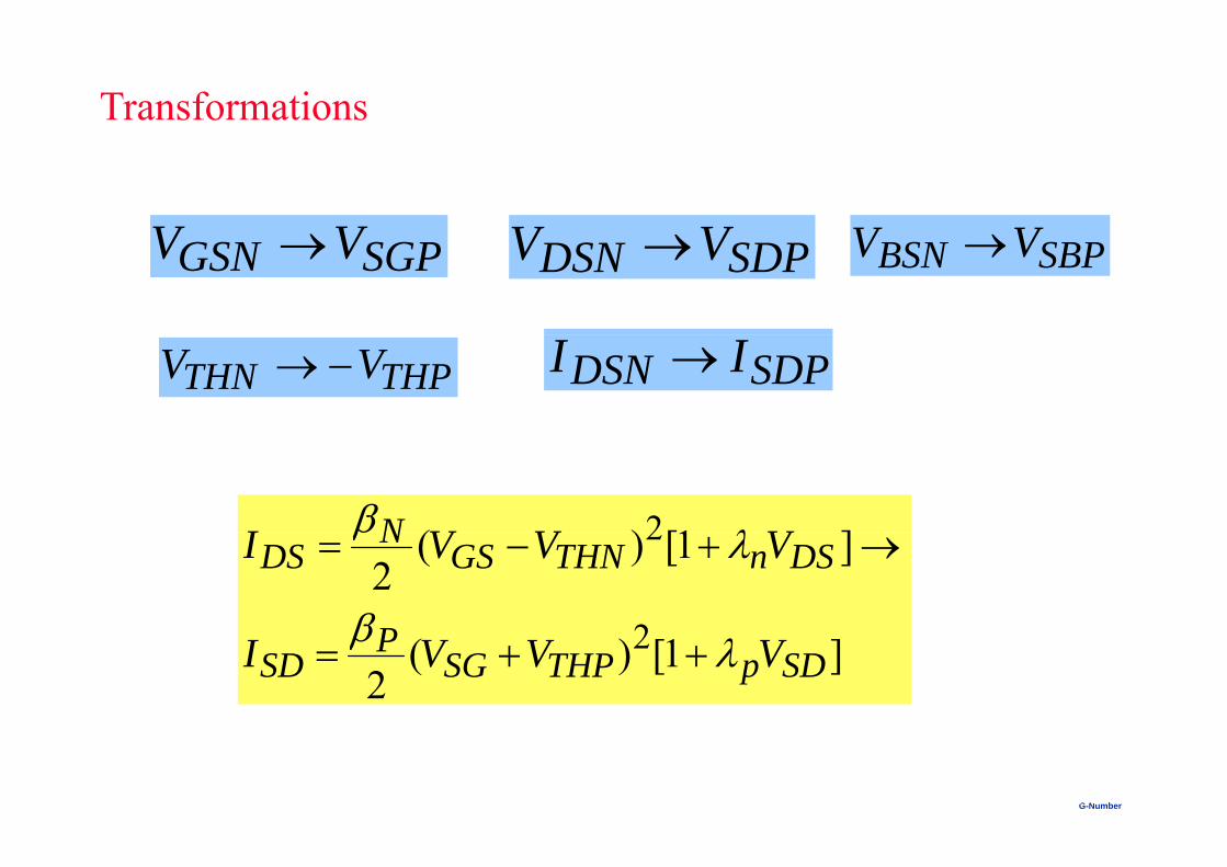
Transformations
VV VV VV SGPGSN VV SDPDSN VV SBPBSN VV
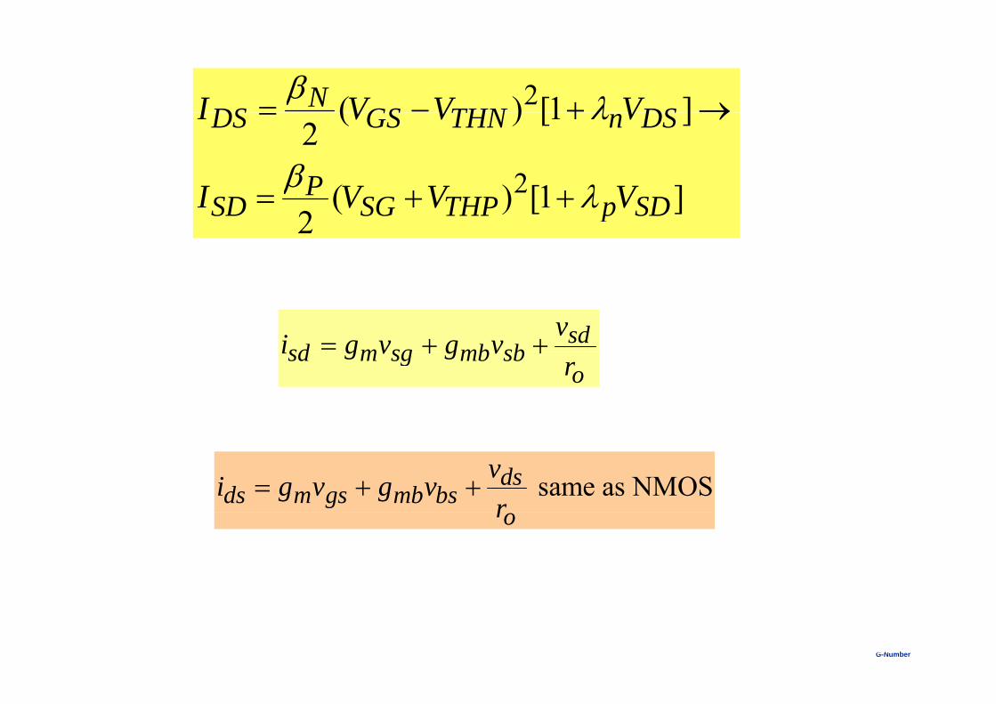
THPTHN VV SDPDSN II
]1[)( 2N VVVI ]1[)(2
2
2
P
DSnTHNGSN
DS VVVI
]1[)(2
2SDpTHPSG
PSD VVVI
G-NumberB. Mazhari, IITK108
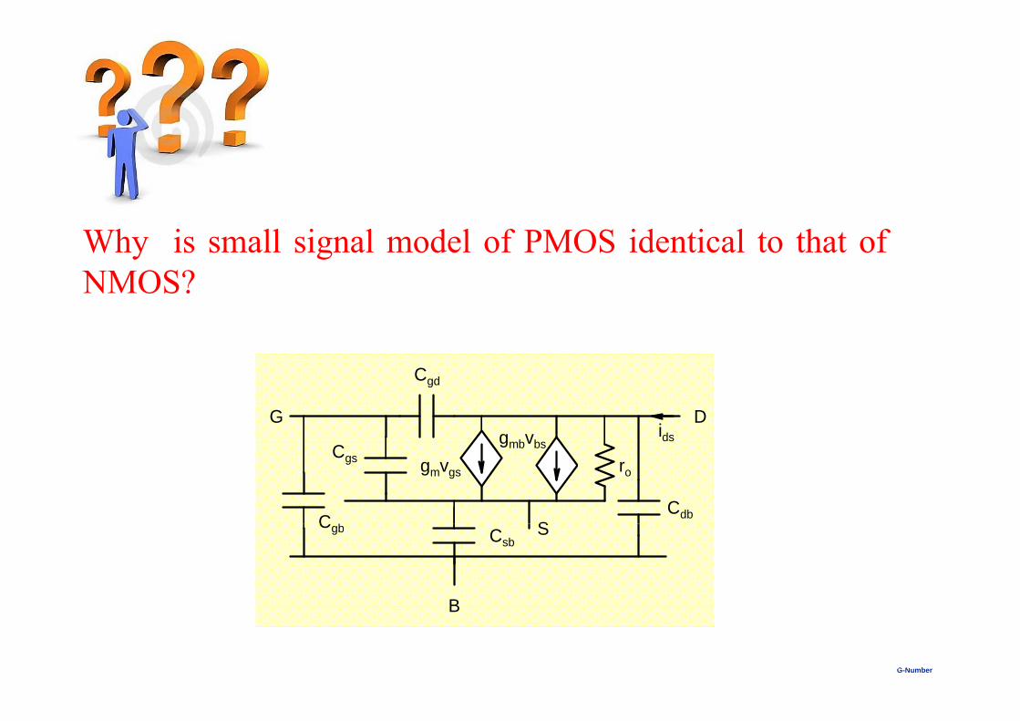
Why is small signal model of PMOS identical to that ofNMOS?NMOS?
Cgd
DGidsgmbvbs
gmvgs
Cdb
ro
S
Cgs
C b
gmbvbs
B
CsbSCgb
G-NumberB. Mazhari, IITK109
B
]1[)( 2DSTHNGS
NDS VVVI
]1[)(
]1[)(2
2P
DSnTHNGSDS
VVVI
VVVI
]1[)(2
2SDpTHPSG
PSD VVVI
sdsd m sg mb sb
vi g v g v sd m sg mb sbo
i g v g vr
same as NMOSdsds m gs mb bs
vi g v g vr
or
G-NumberB. Mazhari, IITK110
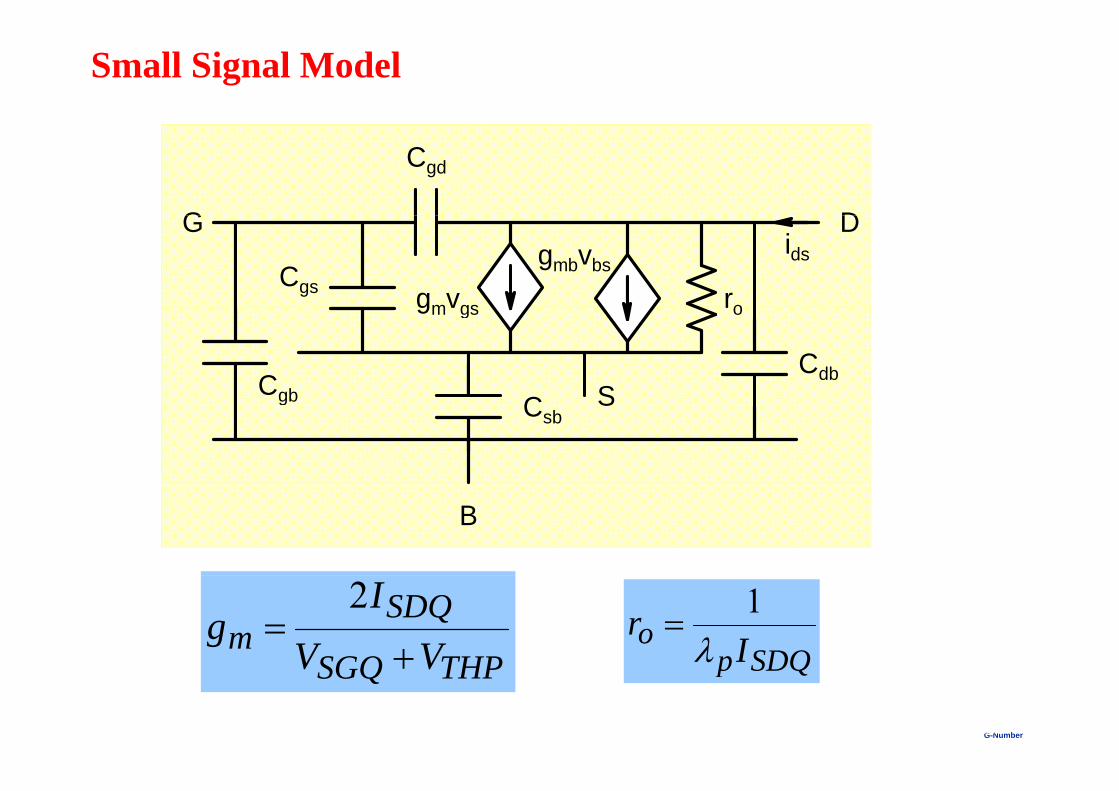
Small Signal Model
Cgd
DG
gmvgs ro
DGids
Cgsgmbvbs
gmvgs
Cdb
ro
SCgb CsbSgb
B
THPSGQ
SDQm VV
Ig
2SDQp
o Ir
1
G-NumberB. Mazhari, IITK111
THPSGQ VV SDQp
We have so far discussed simple MOS models which are suitable for ‘hand-analysis’ of circuits. For more accurate prediction of circuit characteristics using circuit simulation more accurate MOS models are requiredrequired.
SPICE and its various variants are the most popular circuit simulation p ptool. In SPICE, there are a number of MOS models that are available including Level-1, level-2, Level-3, BSIM1, BSIM2, BSIM3, BSIM4 etc.
Level 1 model is the simplest and is basically similar to the large signalLevel-1 model is the simplest and is basically similar to the large signal model that we have described earlier. A popular model for submicron devices is BSIM3 model.
G-NumberB. Mazhari, IITK112
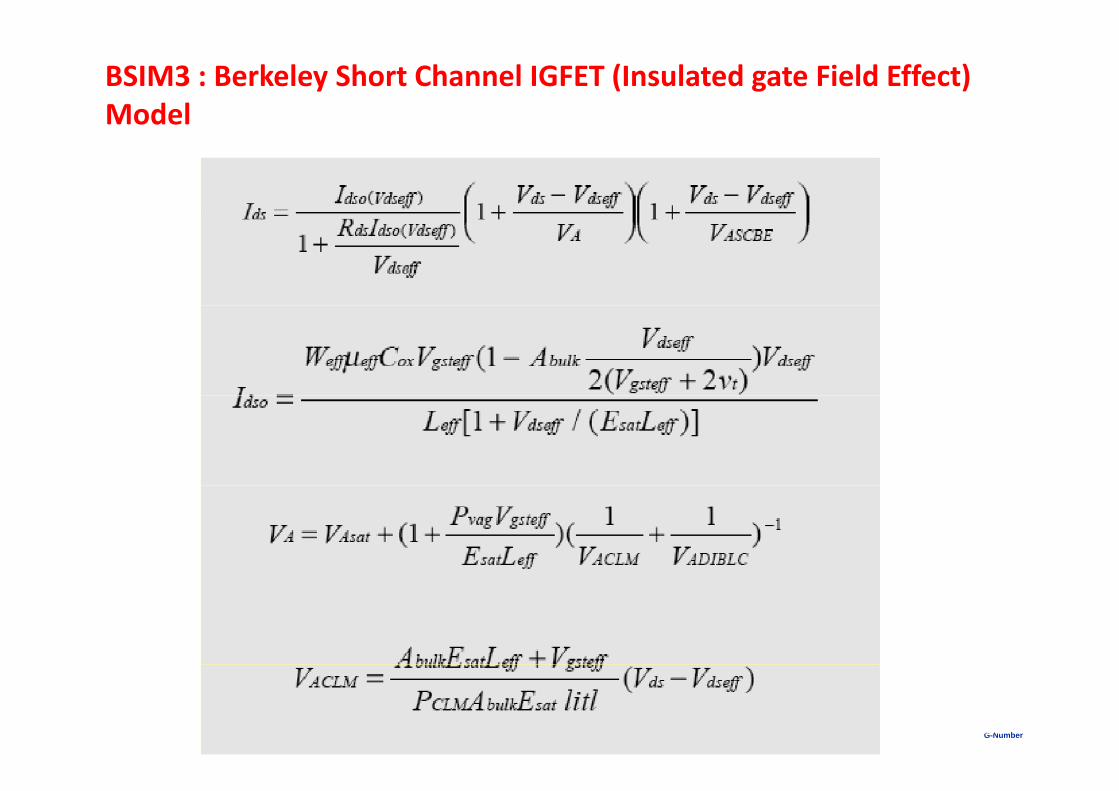
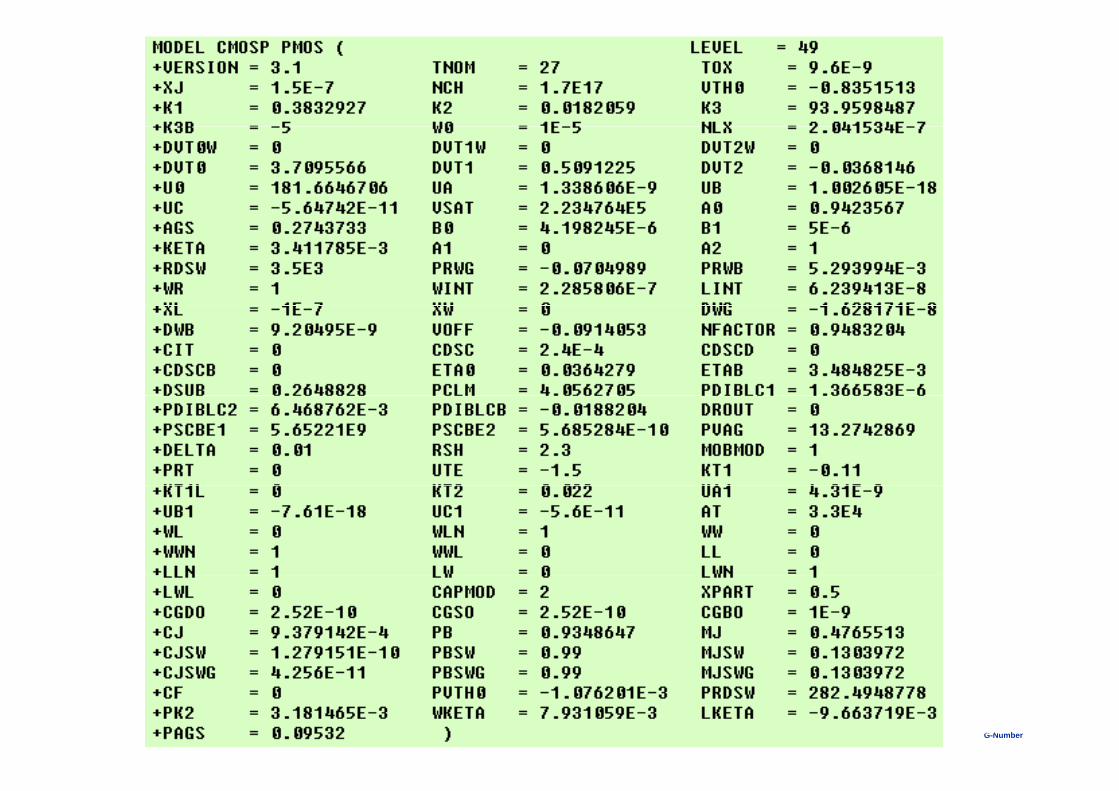
BSIM3 : Berkeley Short Channel IGFET (Insulated gate Field Effect) Model
G-NumberB. Mazhari, IITK113
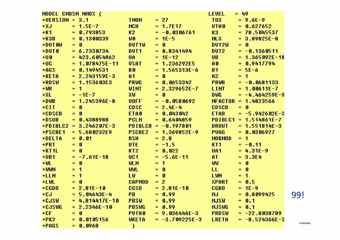
99!
G-NumberB. Mazhari, IITK114
G-NumberB. Mazhari, IITK115
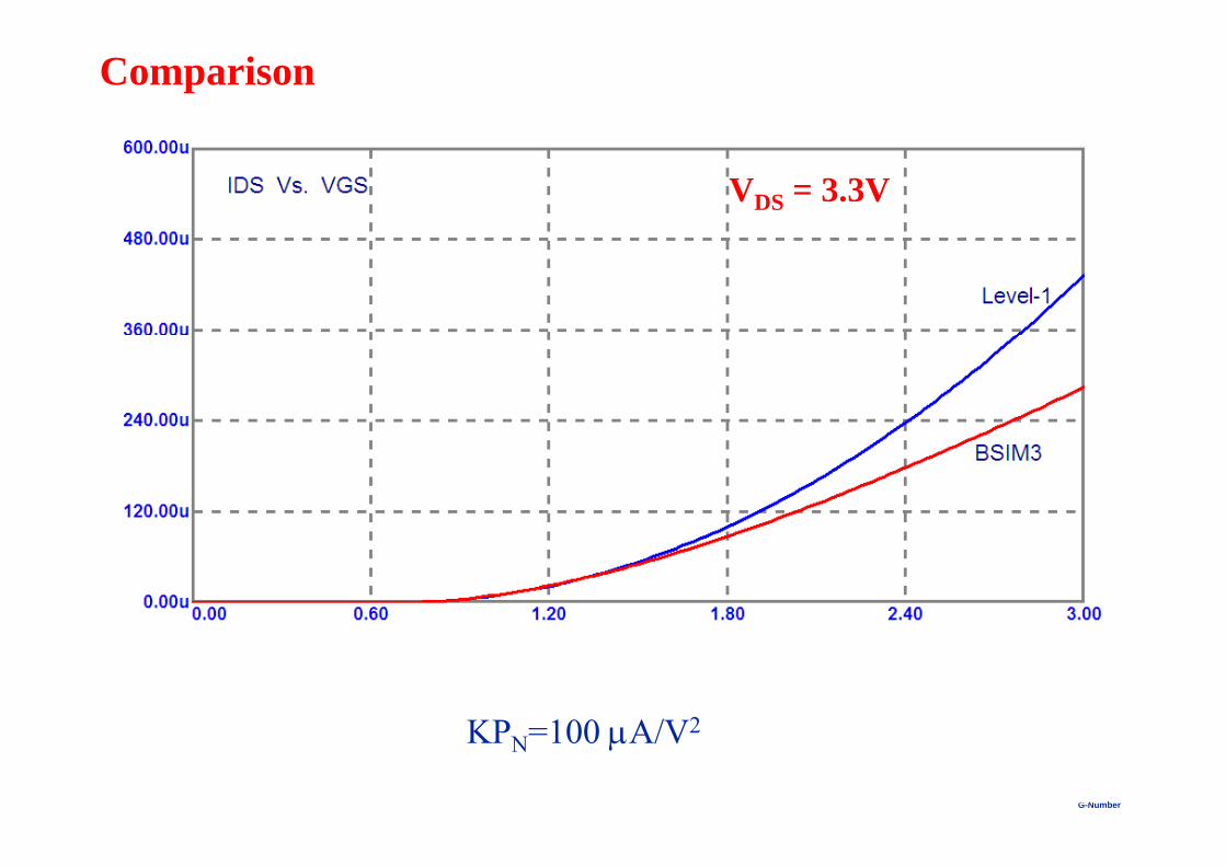
Comparison
VDS = 3.3V
KP 100 A/V2
G-NumberB. Mazhari, IITK116
KPN=100 A/V2
400.0u
500.0u
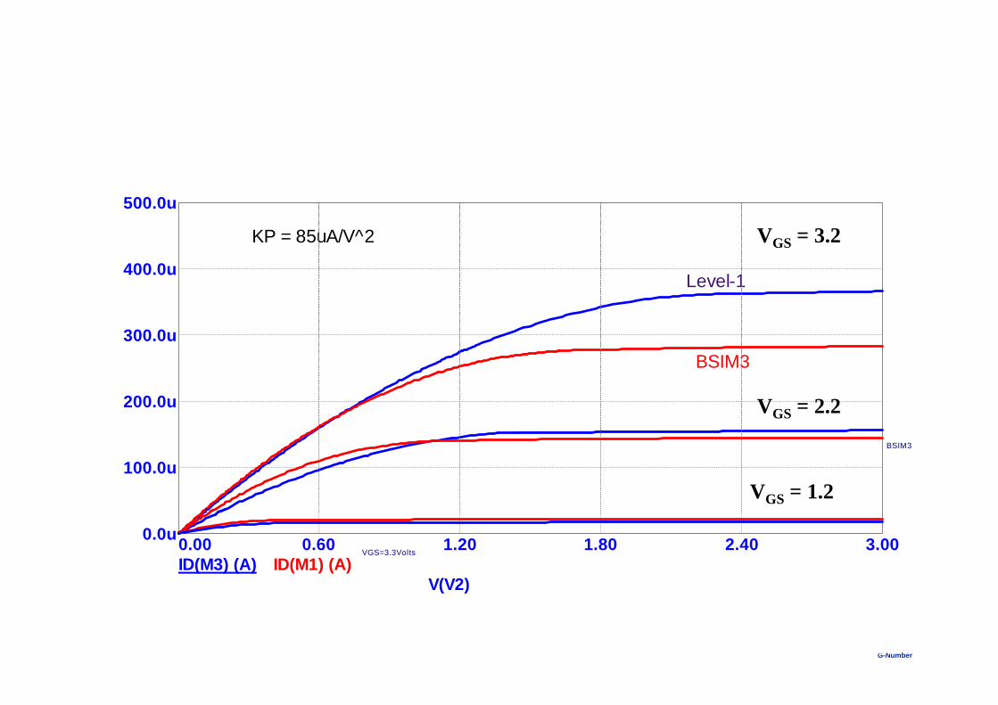
KP = 85uA/V^2 VGS = 3.2
300.0u
400.0uLevel-1
200.0u
BSIM3
VGS = 2.2
100.0uBSIM3
VGS = 1.2
0.00 0.60 1.20 1.80 2.40 3.000.0u
ID(M3) (A)V(V2)
ID(M1) (A)VGS=3.3Volts
G-NumberB. Mazhari, IITK117
( )
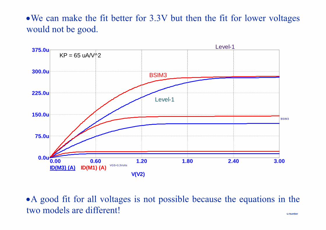
We can make the fit better for 3.3V but then the fit for lower voltageswould not be good.
375.0uKP = 65 uA/V^2
Level-1
300.0u BSIM3
150 0u
225.0uLevel-1
75.0u
150.0uBSIM3
0.00 0.60 1.20 1.80 2.40 3.000.0u
ID(M3) (A) ID(M1) (A) VGS=3.3VoltsID(M3) (A)V(V2)
ID(M1) (A)
G-NumberB. Mazhari, IITK118
A good fit for all voltages is not possible because the equations in thetwo models are different!
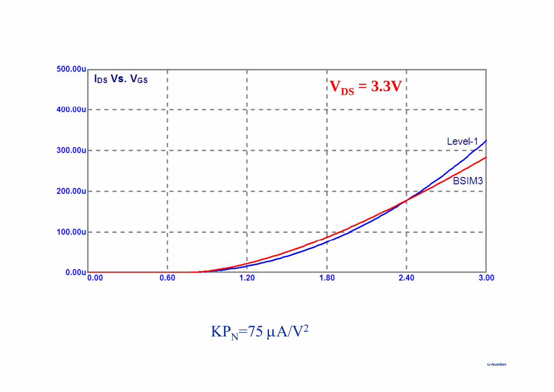
VDS = 3.3V
KP 75 A/V2
G-NumberB. Mazhari, IITK119
KPN=75 A/V2
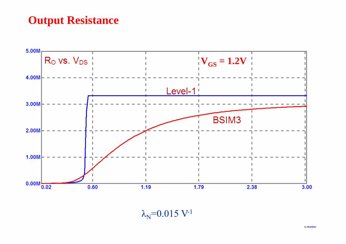
Output Resistance
VGS = 1.2V
G-NumberB. Mazhari, IITK120
λN=0.015 V-1
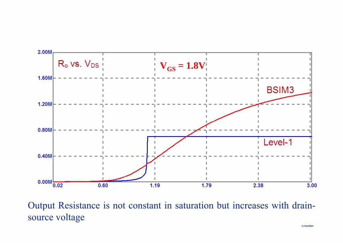
V = 1 8VVGS = 1.8V
Output Resistance is not constant in saturation but increases with drain
G-NumberB. Mazhari, IITK121
Output Resistance is not constant in saturation but increases with drain-source voltage

G-NumberB. Mazhari, IITK122