Embed Size (px)
DESCRIPTION
FYP final report
Citation preview
7/15/2019 EKT445/446 FYP report
http://slidepdf.com/reader/full/ekt445446-fyp-report 1/66
IMPLEMENTATION OF FPGA-BASED ANN
FOR CHARACTER RECOGNITION
LEE YEE ANN
7/15/2019 EKT445/446 FYP report
http://slidepdf.com/reader/full/ekt445446-fyp-report 2/66
IMPLEMENTATION OF FPGA-BASED ANN
FOR CHARACTER RECOGNITION
by
LEE YEE ANN

7/15/2019 EKT445/446 FYP report
http://slidepdf.com/reader/full/ekt445446-fyp-report 3/66
ACKNOWLEDGEMENT
First of all I would like the express my gratitude to God for giving me this chance to
study here in UniMAP and to be able to complete this FPGA implementation of ANN
for character recognition project as my final year project.
I would also like to thank my project supervisor, Dr. PhakLen EhKan, from the bottom
of my heart for his endless encouragement, help, support and guidance throughout the
duration of implementing this final year project. His guidance on how to execute this
project, and how to write an academic and engineering report was extremely helpful and
is very useful for my future.
Next, my sincere appreciation goes to Universiti Malaysia Perlis and the School of
Computer and Communication Engineering for giving me the opportunity to further my
7/15/2019 EKT445/446 FYP report
http://slidepdf.com/reader/full/ekt445446-fyp-report 4/66
APPROVAL AND DECLARATION SHEET
This project report titled “Implementation of FPGA-based ANN for Character
Recognition” was prepared and submitted by Lee Yee Ann (Matrix Number:
101230415) and has been found satisfactory in terms of scope, quality andpresentation as partial fulfillment of the requirement for the Bachelor of
Engineering (Hons.) (Computer Network Engineering) in Universiti Malaysia
Perlis (UniMAP).
Checked and Approved by
7/15/2019 EKT445/446 FYP report
http://slidepdf.com/reader/full/ekt445446-fyp-report 5/66
PELAKSANAAN RANGKAIAN NEURON TIRUAN MENGGUNAKAN FPGA
BAGI PENGECAMAN AKSARA
ABSTRAK
Projek ini merupakan satu titik permulaan untuk mempelajari rangkaian neural buatan
(ANN). Projek ini menyingkap satu pendekatan untuk pelaksanaan ANN berasaskan
perkakasan dengan menggunakan FPGA. Bagi menunjukkan salah satu fungsi ANN
berasaskan FPGA ini, ANN tersebut dilatih untuk mengecam sehingga 16 corak aksara
dalam grid 4×4. Projek ini dibangunkan menggunakan bahasa VHDL dan dikompil
menggunakan perisian Altera QuartusII. Fail-fail yang dihasilkan selepas dikompil
kemudian diprogram ke dalam peranti FPGA Altera CycloneII yang terdapat di atas kit
7/15/2019 EKT445/446 FYP report
http://slidepdf.com/reader/full/ekt445446-fyp-report 6/66
ABSTRACT
This project can be seen as a starting point for learning artificial neural network(ANN).
It explores an approach of hardware based implementation of ANN using FPGA. To
demonstrate the functionality of the FPGA implementation of ANN, the ANN is trained
to recognise up to 16 character patterns on a 4×4 grid. The development of this project
is done by using VHDL and compiled using Altera QuartusII software. The resulting
design files is programmed into the Altera CycloneII FPGA on the Altera DE2
development and education board. In this project, the ANN is designed to be a 3-layer
feed-forward neural network. The ANN learns by applying the backward propagation
7/15/2019 EKT445/446 FYP report
http://slidepdf.com/reader/full/ekt445446-fyp-report 7/66
TABLE OF CONTENTS
Page
ACKNOWLEDGEMENT ii
APPROVAL AND DECLARATION SHEET iii
ABSTRAK iv
ABSTRACT v
TABLE OF CONTENTS vi
LIST OF TABLES ix
LIST OF FIGURES x
LIST OF ABBREVIATIONS xi
7/15/2019 EKT445/446 FYP report
http://slidepdf.com/reader/full/ekt445446-fyp-report 8/66
2.3.1 Field-Programmable Gate Array 13
2.3.2 Very High Speed Integrated Circuit Hardware Description Language 142.3.3 Altera QuartusII 15
2.4 Hardware Components 16
2.4.1 Altera DE2 Development & Education Board 17
2.5 Conclusion 19
CHAPTER 3 METHODOLOGY 21
3.1 Introduction 21
3.2 Project Phases 21
3.2.1 Project Study 21
3.2.2 Planning the Architecture, Algorithm, and Learning Rule of the 22
ANN on FPGA
3.2.3 Develop the VHDL Code in Altera QuartusII Software 23
3.2.4 Perform Simulation on Altera QuartusII Software 23
3.2.5 Download the VHDL Code onto Altera DE2 Development Board 23
7/15/2019 EKT445/446 FYP report
http://slidepdf.com/reader/full/ekt445446-fyp-report 9/66
CHAPTER 4 RESULT AND DISCUSSION 29
4.1 Introduction 29
4.2 Top Level Entity 29
4.2.1 FPGA Device's Resources Used 29
4.3 Result 31
4.4 Discussion 34
4.5 Conclusion 37
CHAPTER 5 CONCLUSION 38
5.1 Introduction 38
5.2 Conclusion 38
5.3 Future Works 39
5.4 Potential Commercialisation 39

7/15/2019 EKT445/446 FYP report
http://slidepdf.com/reader/full/ekt445446-fyp-report 10/66
LIST OF TABLES
Table No. Table Title Page
4.1 Character Pattern and Its Expected Output 31
7/15/2019 EKT445/446 FYP report
http://slidepdf.com/reader/full/ekt445446-fyp-report 11/66
LIST OF FIGURES
Figure No. Figure Title Page
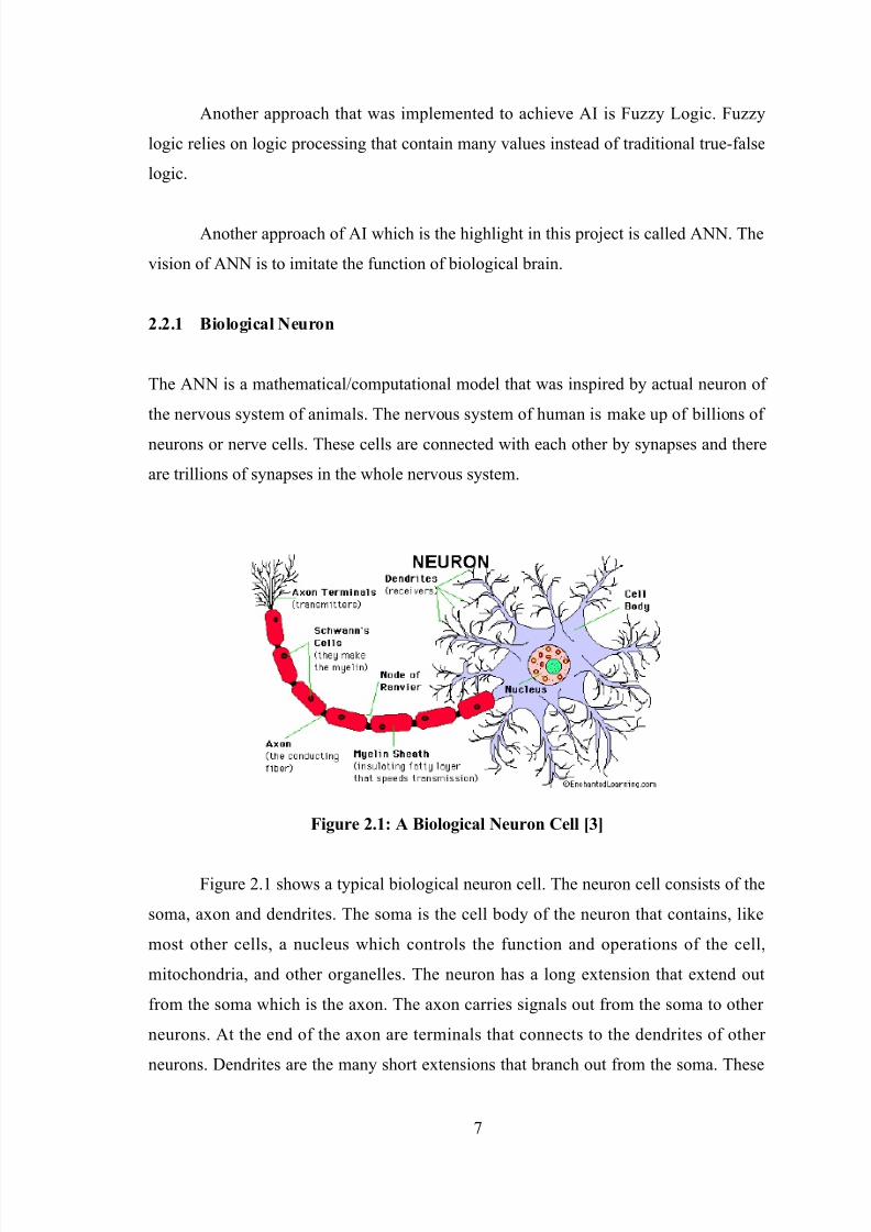
2.1 A Biological Neuron Cell 7
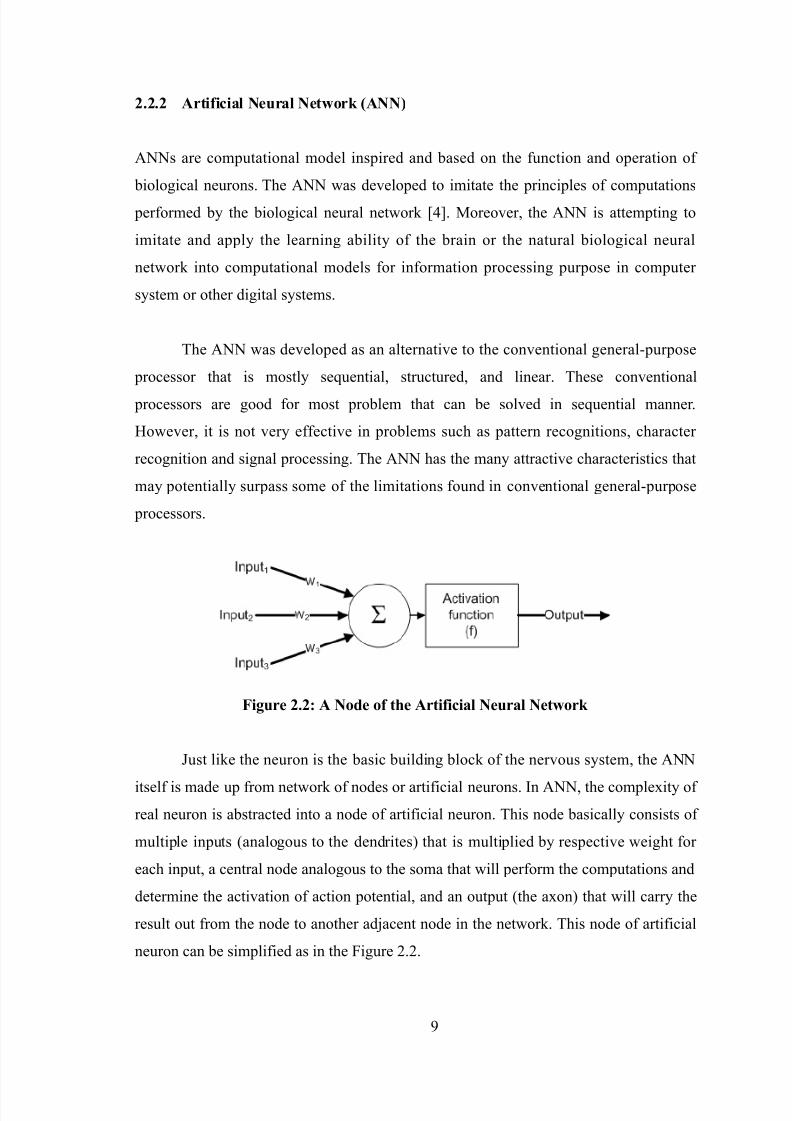
2.2 A Node of the Artificial Neural Network 9
2.3 Single Layer ANN 10
2.4 Small Multi-Layer ANN 10
2.5 Complex Multi-Layer ANN 11
2.6 Altera QuartusII Web Edition Software Version 9.1 SP2 16
2.7 Altera DE2 Development & Education Board 18
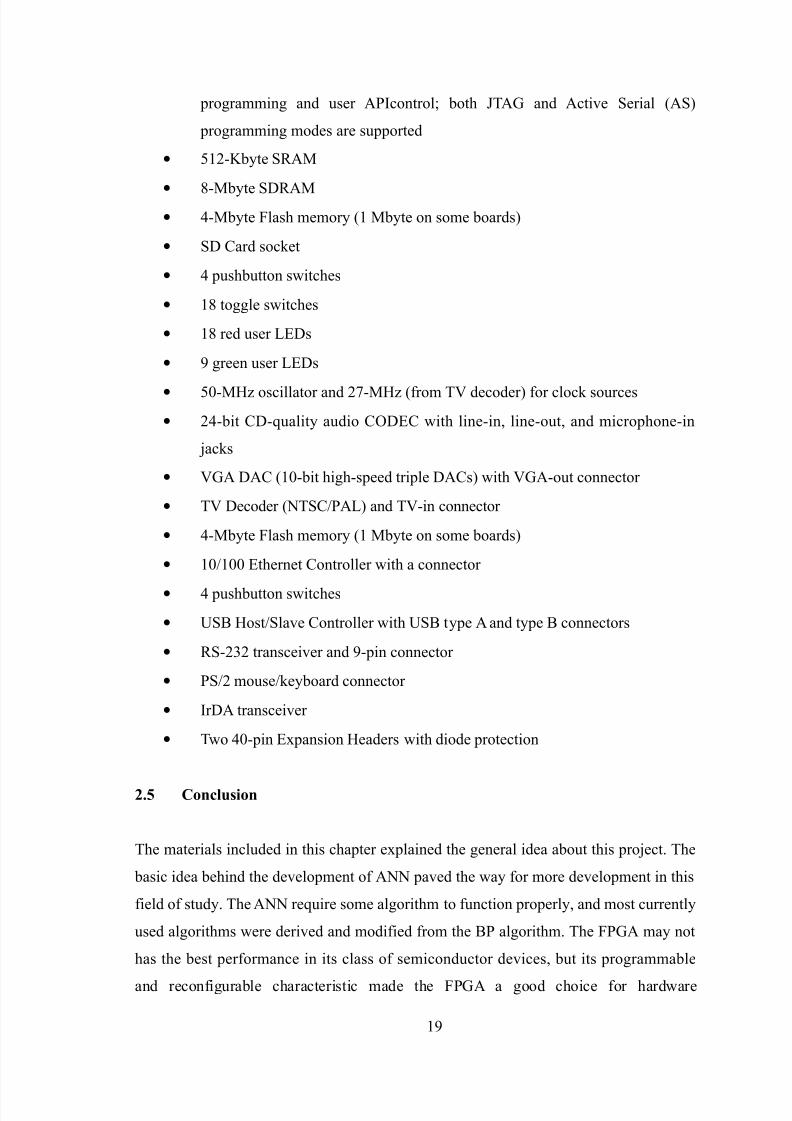
2.8 Layout of Altera DE2 Development & Education Board 18
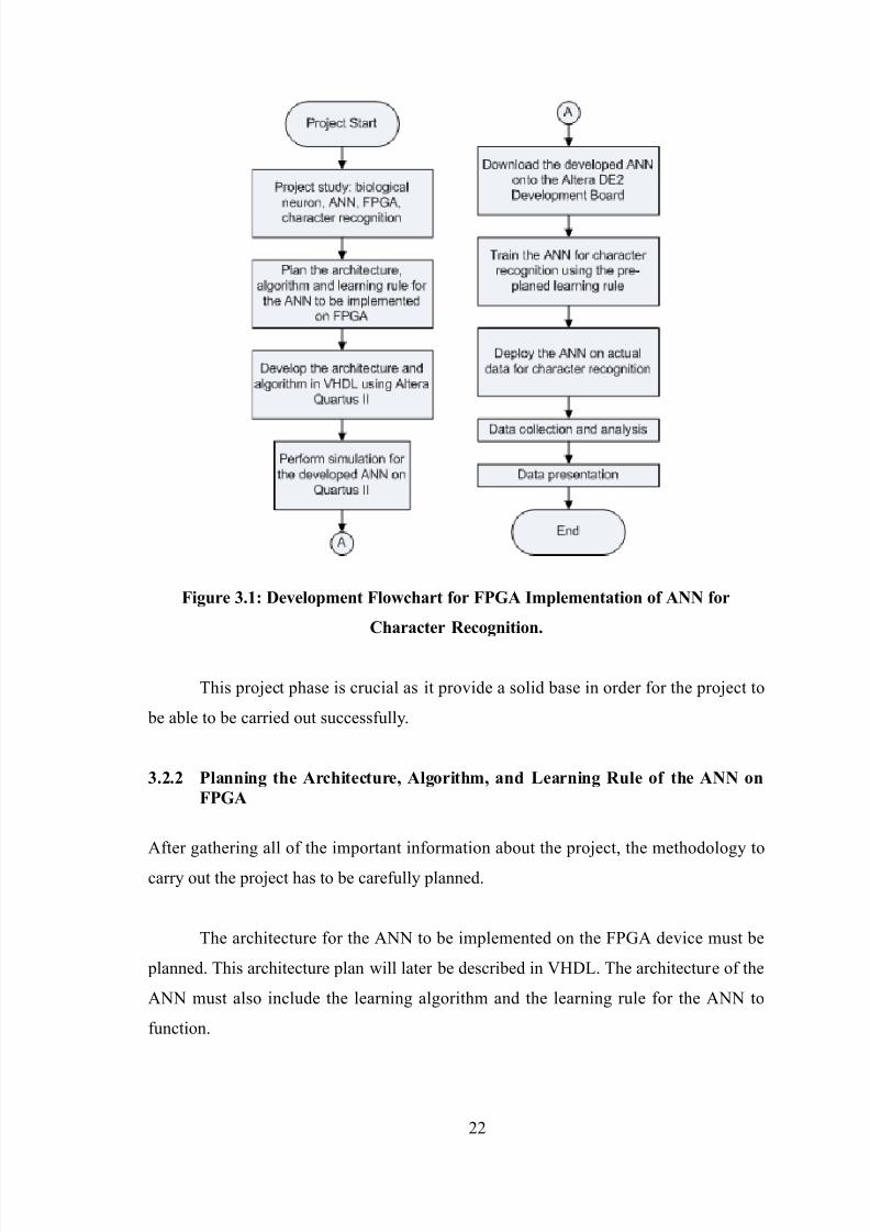
3.1 Development Flowchart for FPGA Implementation of ANN for 22
7/15/2019 EKT445/446 FYP report
http://slidepdf.com/reader/full/ekt445446-fyp-report 12/66
LIST OF ABBREVIATIONS
AI Artificial Intelligence
ANN Artificial Neural Network
ASIC Application-Specific Integrated Circuit
BP Back Propagation
CAD Computer Aided Drafting
CPLD Complex Programmable Logic Device
CPU Central Processing Unit
FPGA Field-Programmable Gate Array
HDL Hardware Description Language
IC Integrated Circuit
7/15/2019 EKT445/446 FYP report
http://slidepdf.com/reader/full/ekt445446-fyp-report 13/66
CHAPTER 1
INTRODUCTION
1.1 Introduction
The human brain is the most complex system of the human body. Consisting of billions
of neurons, the brain is capable of performing extraordinary tasks. The brain is
generally accepted as the CPU that controls every function performed by the human
body similar to the processor or CPU of a computer system.
7/15/2019 EKT445/446 FYP report
http://slidepdf.com/reader/full/ekt445446-fyp-report 14/66
This project is aimed to implement an ANN on FPGA. These include the basic
functional structure and architecture of ANN, the algorithms to run the ANN and the
learning rules to train the ANN to produce the expected result. In order to demonstrate
the operation of the ANN implemented on the FPGA, the system will be trained to
recognise certain characters. Besides, the history of ANN will briefly be explored, the
basic function, building block, and the algorithm of ANN will be explained, and all of
these will be implemented using VHDL and programmed into an FPGA device.
1.2 Problem Statement
The ANN is complicated and complex to be implemented. It involves modelling the
function of biological neuron, developing an algorithm for the ANN to function, and to
train the ANN to perform its tasks accordingly. Since its initial model by McCulloch
and Pitts in 1940's, the research and development of ANN had seen a tremendous
progress.
7/15/2019 EKT445/446 FYP report
http://slidepdf.com/reader/full/ekt445446-fyp-report 15/66
Hardware implementation of ANN using ASIC faced another issue due to the
high cost that came from the development of the complex ANN circuit, the process to
produce the IC, and the lack of demand for ASIC based ANN devices. Furthermore,
ASIC based ANN is application specific and cannot be reconfigured for other purposes.
This is where FPGA based implementation of ANN comes into perspective. Previously,
the FPGA was not seriously considered as the hardware base for implementation of
ANN mainly due to its poor performance in yesteryears, but the advancement in FPGA
technologies nowadays made ANN implementation on FPGA possible. Moreover,
despite the FPGA has considerably inferior performance than ASIC, the flexibility
offered by FPGA made it better choice for small-scale implementation of ANN, and it is
also possible to reconfigure the FPGA according to the ANN to be implemented.
Digital systems require an algorithm or some other methods to recognise
characters. Human beings are familiar with recognition tasks such as recognition of
characters. These characters may be in the form of written characters that form a part of
a string of text to convey information. However to a digital system, this task is not as
7/15/2019 EKT445/446 FYP report
http://slidepdf.com/reader/full/ekt445446-fyp-report 16/66
• To compare the output from the ANN with the actual result.
1.4 Contribution
This research will introduce a new hardware based implementation of ANN and also a
new FPGA architecture for implementing an ANN.
The implementation of ANN on hardware as in FPGA is expected to overcome
the slower processing speed of current software based implementation of ANN. This
project will also introduce an application of ANN such as character recognition.
1.5 Scope of Study
This research is limited to the following scope of study.
• The development of the ANN architecture will be done using VHDL.
• The learning algorithm to be implemented for the FPGA implementation of
ANN is based on a slightly modified BP algorithm.

7/15/2019 EKT445/446 FYP report
http://slidepdf.com/reader/full/ekt445446-fyp-report 17/66
and its learning algorithm, the HDL used in this project, and the FPGA. This chapter
also explore the related works regarding this project and the tools used throughout the
project.
Chapter 3 will explain the steps taken to implement the ANN on FPGA device
and to apply the developed ANN for character recognition.
Chapter 4 demonstrates the result from the project. The result is analysed and
compared to the desired result.
Chapter 5 concludes the whole project and provides a few things that can be
improved concerning the project in the future.
7/15/2019 EKT445/446 FYP report
http://slidepdf.com/reader/full/ekt445446-fyp-report 18/66
CHAPTER 2
LITERATURE REVIEW
2.1 Introduction
This chapter aims to provide basic information about the project. The chapter starts by
introducing the terminologies such as the biological neuron, ANN, FPGA, and VHDL.
These terms is discussed as how it related with the project.
Next, the development tool used throughout the project is introduced and
7/15/2019 EKT445/446 FYP report
http://slidepdf.com/reader/full/ekt445446-fyp-report 19/66
Another approach that was implemented to achieve AI is Fuzzy Logic. Fuzzy
logic relies on logic processing that contain many values instead of traditional true-false
logic.
Another approach of AI which is the highlight in this project is called ANN. The
vision of ANN is to imitate the function of biological brain.
2.2.1 Biological Neuron
The ANN is a mathematical/computational model that was inspired by actual neuron of
the nervous system of animals. The nervous system of human is make up of billions of
neurons or nerve cells. These cells are connected with each other by synapses and there
are trillions of synapses in the whole nervous system.
7/15/2019 EKT445/446 FYP report
http://slidepdf.com/reader/full/ekt445446-fyp-report 20/66
dendrites are signal receivers that carry signals from other neuron cells into the soma.
The axons and dendrites are not directly connected or coupled together, instead the
signal carried by axon of one neuron are transmitted to the dendrites of other neurons
over a very small gaps called the synapses.
Neurons send and receive signals in electrical-chemical form called nerve
impulses or action potentials. The function of a biological neuron can be described as:
1. The dendrites of the neuron will receive signals, or action potentials,
transmitted by adjacent axons and carry these signals into the cell body (the
soma).
2. The signals from all the dendrites of the neuron are added together or
processed. The result of the processed signals are determine if it is strong
enough or surpasses a certain threshold value.
3. If it exceed the threshold, that neuron will generate an action potential.
4. This action potential will then propagate along the axon to the synapses
between itself and other adjacent neurons or other cells.
5. This action potential that is transmitted over the synapses will in turn excite
7/15/2019 EKT445/446 FYP report
http://slidepdf.com/reader/full/ekt445446-fyp-report 21/66
2.2.2 Artificial Neural Network (ANN)
ANNs are computational model inspired and based on the function and operation of
biological neurons. The ANN was developed to imitate the principles of computations
performed by the biological neural network [4]. Moreover, the ANN is attempting to
imitate and apply the learning ability of the brain or the natural biological neural
network into computational models for information processing purpose in computer
system or other digital systems.
The ANN was developed as an alternative to the conventional general-purpose
processor that is mostly sequential, structured, and linear. These conventional
processors are good for most problem that can be solved in sequential manner.
However, it is not very effective in problems such as pattern recognitions, character
recognition and signal processing. The ANN has the many attractive characteristics that
may potentially surpass some of the limitations found in conventional general-purpose
processors.
7/15/2019 EKT445/446 FYP report
http://slidepdf.com/reader/full/ekt445446-fyp-report 22/66
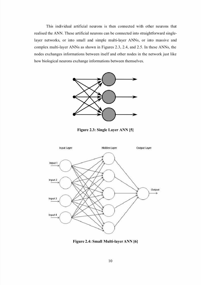
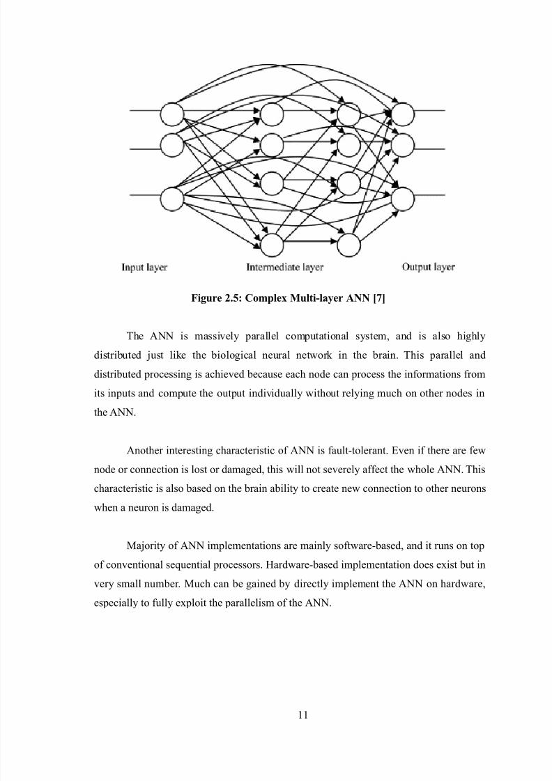
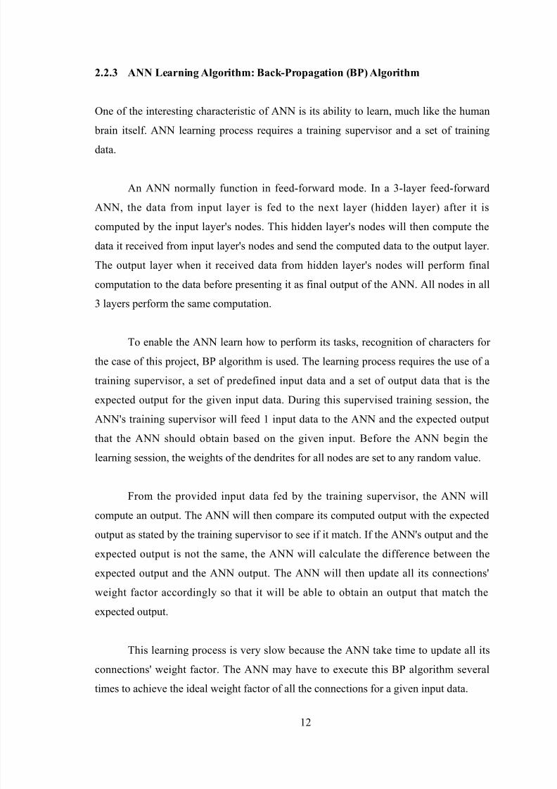
This individual artificial neurons is then connected with other neurons that
realised the ANN. These artificial neurons can be connected into straightforward single-
layer networks, or into small and simple multi-layer ANNs, or into massive and
complex multi-layer ANNs as shown in Figures 2.3, 2.4, and 2.5. In these ANNs, the
nodes exchanges informations between itself and other nodes in the network just like
how biological neurons exchange informations between themselves.
Figure 2.3: Single Layer ANN [5]
7/15/2019 EKT445/446 FYP report
http://slidepdf.com/reader/full/ekt445446-fyp-report 23/66
Figure 2.5: Complex Multi-layer ANN [7]
The ANN is massively parallel computational system, and is also highly
distributed just like the biological neural network in the brain. This parallel and
distributed processing is achieved because each node can process the informations from
7/15/2019 EKT445/446 FYP report
http://slidepdf.com/reader/full/ekt445446-fyp-report 24/66
2.2.3 ANN Learning Algorithm: Back-Propagation (BP) Algorithm
One of the interesting characteristic of ANN is its ability to learn, much like the human
brain itself. ANN learning process requires a training supervisor and a set of training
data.
An ANN normally function in feed-forward mode. In a 3-layer feed-forward
ANN, the data from input layer is fed to the next layer (hidden layer) after it is
computed by the input layer's nodes. This hidden layer's nodes will then compute the
data it received from input layer's nodes and send the computed data to the output layer.
The output layer when it received data from hidden layer's nodes will perform final
computation to the data before presenting it as final output of the ANN. All nodes in all
3 layers perform the same computation.
To enable the ANN learn how to perform its tasks, recognition of characters for
the case of this project, BP algorithm is used. The learning process requires the use of a
training supervisor, a set of predefined input data and a set of output data that is the
7/15/2019 EKT445/446 FYP report
http://slidepdf.com/reader/full/ekt445446-fyp-report 25/66
The ANN will then repeats the same learning process and BP algorithm on the
other data in the training data set. All input data in the training data set has its own
expected output data. Therefore the ANN will have to learn all the expected output for
all input data in the training data set. This learning process takes some times to be
completed.
An BP algorithm is the most used learning algorithm for training an ANN. Other
learning algorithms do exist but most of these algorithms are based on the BP algorithm.
2.3 Development Tools
The development of this project will be done by using VHDL. There are some
development tools or IDEs that can be used for project development using VHDL.
Companies such as Xilinx Inc. and Altera Corporation are very active in this field. They
are major producers of FPGA chips and had developed several development tools. The
Altera Quartus II software is used throughout this project,.
7/15/2019 EKT445/446 FYP report
http://slidepdf.com/reader/full/ekt445446-fyp-report 26/66
FPGA very suitable for research and prototyping purposes before the design is
submitted for fabrication on ASICs. FPGAs are also able to handle dense logic and
memory elements offering very high logic capacity [10].
However the FPGA is relatively much slower than other hard-wired devices. The
device itself is more expensive than any other hard-wired devices. The internal structure
of FPGA is more complex to provide the reprogrammable ability.
2.3.2 Very High Speed Integrated Circuit Hardware Description Language
(VHDL)
Hardware description language (HDL) is a type of computer language used to describe
and design the structure, operation and behaviour of electronic circuits or systems,especially digital electronic circuits or digital systems [11]. There are many HDLs exist.
The 2 most widely-used HDLs are the VerilogHDL (shorted to Verilog) and the Very
High Speed Integrated Circuit Hardware Description Language (VHSIC HDL or simply
VHDL). For the purpose of this project, VHDL is used to describe the entity,
7/15/2019 EKT445/446 FYP report
http://slidepdf.com/reader/full/ekt445446-fyp-report 27/66
The disadvantages on the other hand are that VHDL is complicated and
confusing for beginners. One of the advantage of VHDL that can be seen as confusing is
that in VHDL, there are many different ways of modelling the same design, architecture
or behaviour [14].
2.3.3 Altera Quartus II
As one of the main contender in the FPGA field, Altera had developed its own suite of
development tools to be used for developments of new systems or prototypes using its
FPGAs. The main development software for designing with CPLDs, FPGAs from
Altera is the Altera Quartus II.
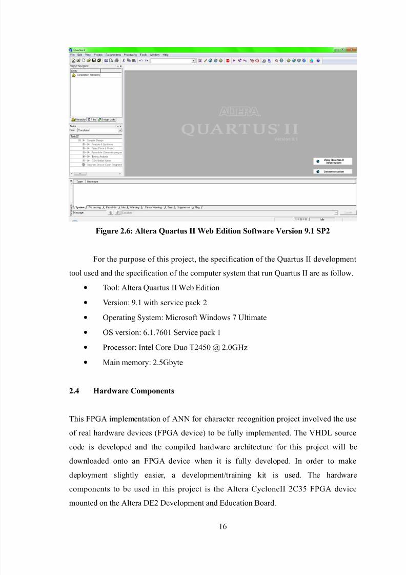
The Altera Quartus II is a complete suite of development tools. As of version
9.1, the Quartus II software contains all of the required tool for development of systems
or prototypes with Altera's CPLDs and FPGAs devices.
7/15/2019 EKT445/446 FYP report
http://slidepdf.com/reader/full/ekt445446-fyp-report 28/66
Figure 2.6: Altera Quartus II Web Edition Software Version 9.1 SP2
For the purpose of this project, the specification of the Quartus II development
tool used and the specification of the computer system that run Quartus II are as follow.
7/15/2019 EKT445/446 FYP report
http://slidepdf.com/reader/full/ekt445446-fyp-report 29/66
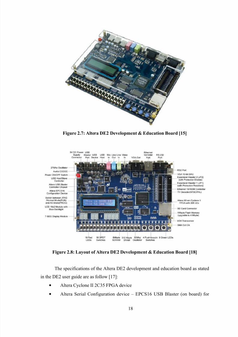
2.4.1 Altera DE2 Development & Education Board
The Altera DE2 development and education board is one of the training/development
kits developed by Altera Corporation. This development kit is aimed to be used by the
universities and other educational institutions. Altera DE2 is distributed by Terasic
Technologies Inc.
The Altera DE2 board provide the ideal support for learning about digital logic,
computer organization, FPGAs, and development and prototyping for multiple purposes
[15]. The board offers all features that make it suitable for laboratory use for university
courses, for a variety of design projects, as well as for the development of sophisticated
digital systems [16].
The main FPGA device of Altera DE2 is the Altera CycloneII EP2C35 FPGA
that has a total of 33,216 Logic Elements, 105 M4K RAM blocks, 483,840 total RAM
bits, 35 embedded multipliers, 4 PLLs, and 475 user I/O pins in a 672-pin FineLine
7/15/2019 EKT445/446 FYP report
http://slidepdf.com/reader/full/ekt445446-fyp-report 30/66
Figure 2.7: Altera DE2 Development & Education Board [15]
7/15/2019 EKT445/446 FYP report
http://slidepdf.com/reader/full/ekt445446-fyp-report 31/66
programming and user APIcontrol; both JTAG and Active Serial (AS)
programming modes are supported
• 512-Kbyte SRAM
• 8-Mbyte SDRAM
• 4-Mbyte Flash memory (1 Mbyte on some boards)
• SD Card socket
•
4 pushbutton switches
• 18 toggle switches
• 18 red user LEDs
• 9 green user LEDs
• 50-MHz oscillator and 27-MHz (from TV decoder) for clock sources
• 24-bit CD-quality audio CODEC with line-in, line-out, and microphone-in
jacks
• VGA DAC (10-bit high-speed triple DACs) with VGA-out connector
• TV Decoder (NTSC/PAL) and TV-in connector
• 4-Mbyte Flash memory (1 Mbyte on some boards)

7/15/2019 EKT445/446 FYP report
http://slidepdf.com/reader/full/ekt445446-fyp-report 32/66
prototyping of new design and architecture. HDL such as the VHDL had made
development of new digital electronic system design and architecture much easier. The
VHDL allows the FPGA to be more flexible in design. The development of the project
will be done using the development tools, FPGA device, and development board from
Altera Corporation. The Altera Quartus II software is used to develop the project and
the project in turn will be implemented onto Altera CycloneII 2C35 FPGA device on the
Altera DE2 board.
7/15/2019 EKT445/446 FYP report
http://slidepdf.com/reader/full/ekt445446-fyp-report 33/66
CHAPTER 3
METHODOLOGY
3.1 Introduction
This chapter will elucidate the steps undertaken in executing the FPGA implementation
of ANN for character recognition project. The methodology started by a study phase
which will then progress to planning and development phase. Later, the project will
enter execution phase and is followed by error recording and correction. The result is
then recorded and analysed before being presented. The project should end when it
7/15/2019 EKT445/446 FYP report
http://slidepdf.com/reader/full/ekt445446-fyp-report 34/66
Figure 3.1: Development Flowchart for FPGA Implementation of ANN for
7/15/2019 EKT445/446 FYP report
http://slidepdf.com/reader/full/ekt445446-fyp-report 35/66
3.2.3 Develop the VHDL Code in Altera Quartus II Software
Once the planning is completed, the architecture, including the learning algorithm and
learning rule, is then translated into VHDL code. The VHDL code is then compiled for
any error and the necessary corrections is made.
The development tool used for this project is the QuartusII software from Altera.
The version of Altera QuartusII used throughout the project is Quartus II version 9.1
Web Edition Service Pack 2.
3.2.4 Perform Simulation on Altera Quartus II Software
When the development of the VHDL code is done and there are no compile error, the
code will be simulated in Altera QuartusII. The simulation result will be carefully
examined for any run-time error. Any detected error has to be corrected.
Correction is done by going back to code development phase and correcting the
7/15/2019 EKT445/446 FYP report
http://slidepdf.com/reader/full/ekt445446-fyp-report 36/66
3.2.7 Deploy the ANN on Actual Data for Character Recognition
The ANN is later on deployed for character recognition application using actual data.
This data is obtained from the user which will input the character pattern to the system.
3.2.8 Data Collection and Analysis
The resulting data obtained from the deployment of the ANN is collected and it is
analysed.
3.2.9 Data Presentation
The analysed data will be presented to be used by others in a format that is easily
understood by other readers.
3.3 Functional Blocks
7/15/2019 EKT445/446 FYP report
http://slidepdf.com/reader/full/ekt445446-fyp-report 37/66
lines and perform a series of calculations. The calculated value (hidden nodes' output) is
again multiplied with the associated weight factor each hidden-output nodes connection
before being fed to the nodes of the output layer of the ANN. This output layer then
perform the same calculations as done by hidden nodes before deciding the actual
output of the system. The outputs from the nodes at the output layer forms the actual
output of the whole system. This operation is called feed-forward operation.
The weight factors associated to each connection between input and hidden
nodes, and the weight factors associated to each connection between hidden and output
nodes are assigned with random number when the ANN is initialised. This random
number is generated by the pseudo-random number generator block.
The ANN only perform feed-forward operations when operating normally to
recognise the user input pattern. However, before the ANN can be used to perform
character recognition tasks or any other tasks, it had to be trained to recognised and
differentiate the different input patterns that may be input by the user. For learning
process, backward propagation algorithm is used. During the learning phase, the ANN is
7/15/2019 EKT445/446 FYP report
http://slidepdf.com/reader/full/ekt445446-fyp-report 38/66
3.3.3 Pseudo-Random Number Generator Block
This block generates pseudo random number to the assigned as the weight factors for all
connections between the input and hidden nodes and all connections between the hidden
and output nodes of the ANN. It has a linear feedback shift-register to generate the
pseudo-random number. This block is used as actual random number generator cannot
be modelled for this project.
3.3.4 Floating Point Processor Block
This functional block is the arithmetic logic unit to perform arithmetic and logic
operations of floating point number for the ANN block and the ANN training supervisor
block. The ANN block and the ANN training supervisor block will provide the floating
point numbers to be processed and provide the desired operations. The floating point
processor will then signal the ANN block and the ANN training supervisor block when
it finish its its operation so that the result can be collected.
7/15/2019 EKT445/446 FYP report
http://slidepdf.com/reader/full/ekt445446-fyp-report 39/66
input data to be displayed on the left side of the LCD text field. It also receive the
output from the ANN and display the recognised character on the LCD module.
3.3.7 LCD Driver Block
LCD driver block is similar to the SRAM driver block as it provide the necessary
abstraction for interfacing with the LCD module on-board the Altera DE2 board. This
block will initialise the on-board LCD module when the system is reset and interfaces
with the on-board LCD module to send custom character data and text string to be
displayed on the LCD module. The custom character data and the text string to be
displayed is obtained from the LCD controller block.
3.3.8 User Input Devices
This system receives input from users through 16 toggle switches out of the 18 toggle
switches and 3 push-button switches out of the 4 available push-button switches on-
board the Altera DE2 board. The 16 toggle switches is used by the users to input the

7/15/2019 EKT445/446 FYP report
http://slidepdf.com/reader/full/ekt445446-fyp-report 40/66
3.4 Conclusion
This chapter had very much summarised all the methodologies involved in the project.
The project is divided into several phases starting with study phase and ends with data
collection, analysis and presentation phase. Beside that, the functional blocks
representing the top-level architecture of the system to be developed on the FPGA is
also explained. Each functional block has its own architecture and behaviour. These
functional blocks are connected together to produce the desired behaviour of the overall
system for this project. Hopefully the material in this chapter will be helpful for future
projects.
7/15/2019 EKT445/446 FYP report
http://slidepdf.com/reader/full/ekt445446-fyp-report 41/66
CHAPTER 4
RESULTS AND DISCUSSION
4.1 Introduction
In this chapter, the outcome of the project FPGA implementation of ANN for character
recognition is presented. The synthesised top level entity of the system is presented and
clearly explained. Then the output from the system is collected and analysed. Some
discussions related to the issues faced by the system and the overall project are included
at the end of the chapter.
7/15/2019 EKT445/446 FYP report
http://slidepdf.com/reader/full/ekt445446-fyp-report 42/66
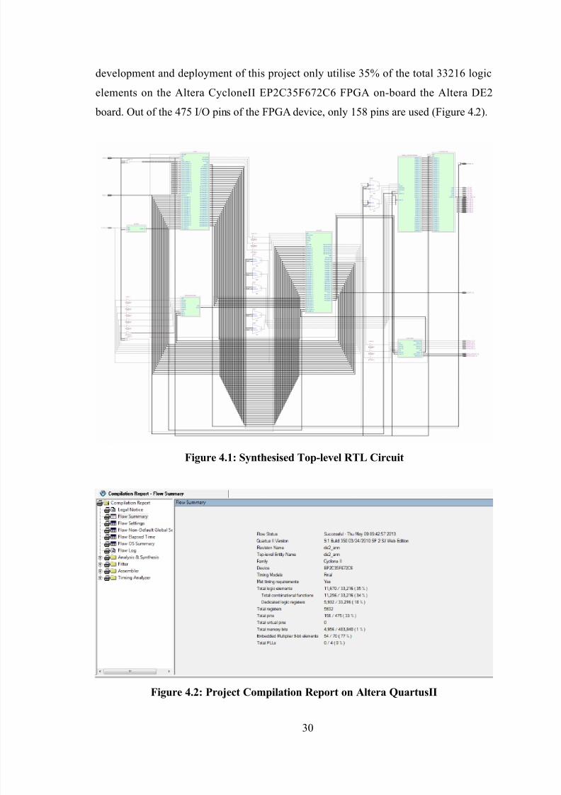
development and deployment of this project only utilise 35% of the total 33216 logic
elements on the Altera CycloneII EP2C35F672C6 FPGA on-board the Altera DE2
board. Out of the 475 I/O pins of the FPGA device, only 158 pins are used (Figure 4.2).
7/15/2019 EKT445/446 FYP report
http://slidepdf.com/reader/full/ekt445446-fyp-report 43/66
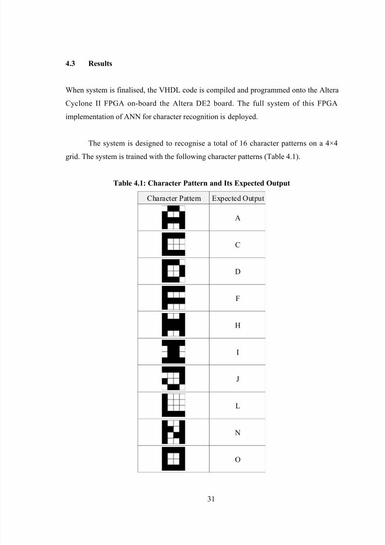
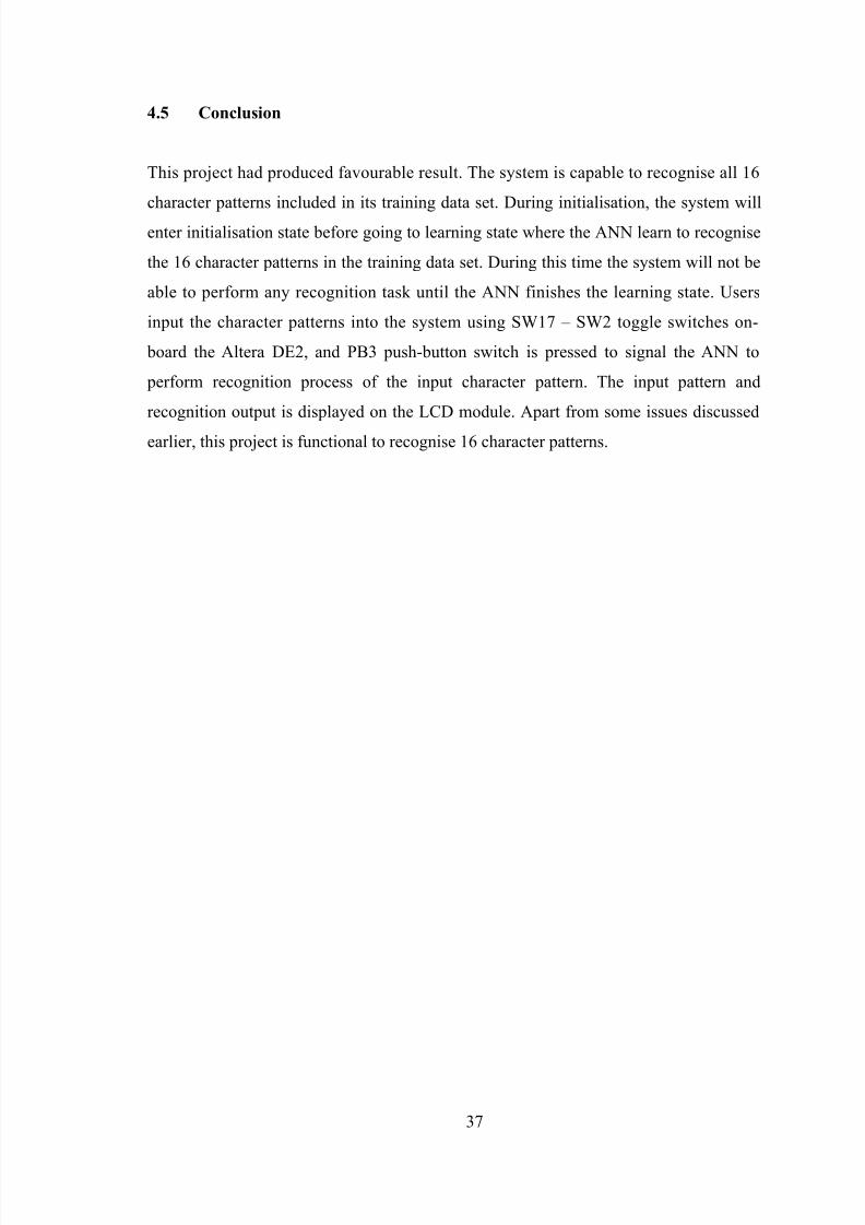
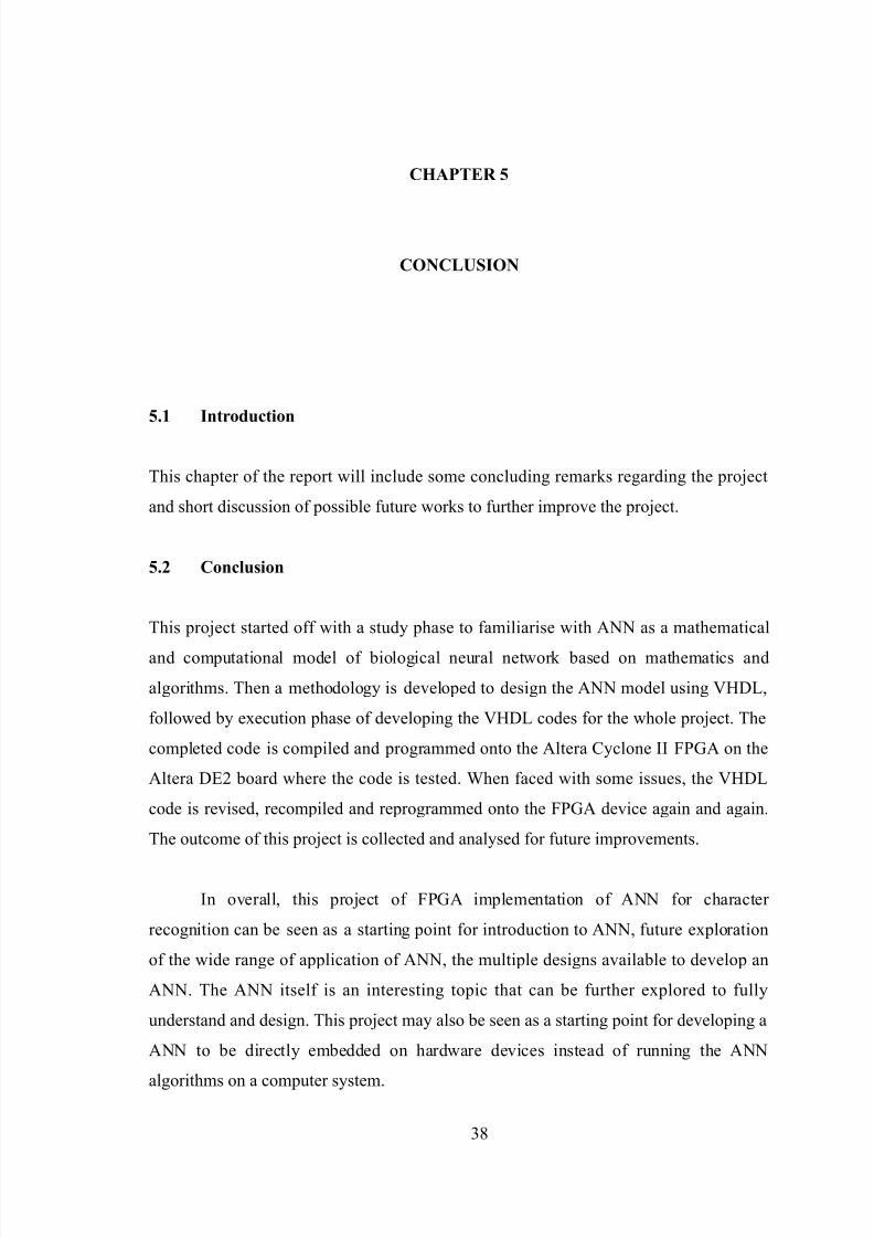
4.3 Results
When system is finalised, the VHDL code is compiled and programmed onto the Altera
Cyclone II FPGA on-board the Altera DE2 board. The full system of this FPGA
implementation of ANN for character recognition is deployed.
The system is designed to recognise a total of 16 character patterns on a 4×4
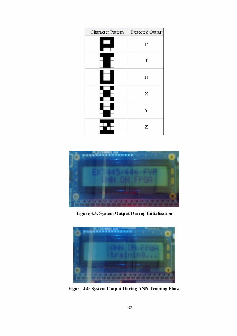
grid. The system is trained with the following character patterns (Table 4.1).
Table 4.1: Character Pattern and Its Expected Output
Character Pattern Expected Output
A
C
7/15/2019 EKT445/446 FYP report
http://slidepdf.com/reader/full/ekt445446-fyp-report 44/66
Character Pattern Expected Output
P
T
U
X
Y
Z
7/15/2019 EKT445/446 FYP report
http://slidepdf.com/reader/full/ekt445446-fyp-report 45/66
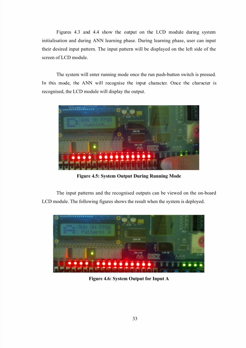
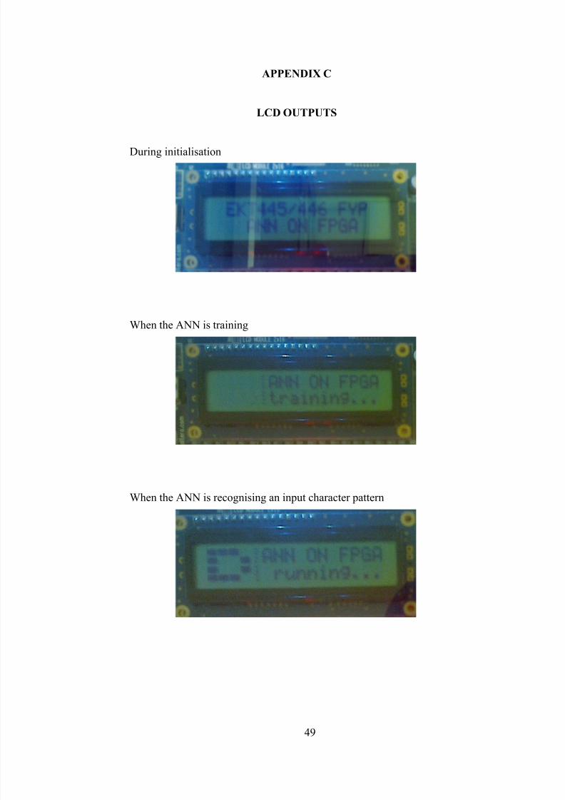
Figures 4.3 and 4.4 show the output on the LCD module during system
initialisation and during ANN learning phase. During learning phase, user can input
their desired input pattern. The input pattern will be displayed on the left side of the
screen of LCD module.
The system will enter running mode once the run push-button switch is pressed.
In this mode, the ANN will recognise the input character. Once the character is
recognised, the LCD module will display the output.
7/15/2019 EKT445/446 FYP report
http://slidepdf.com/reader/full/ekt445446-fyp-report 46/66
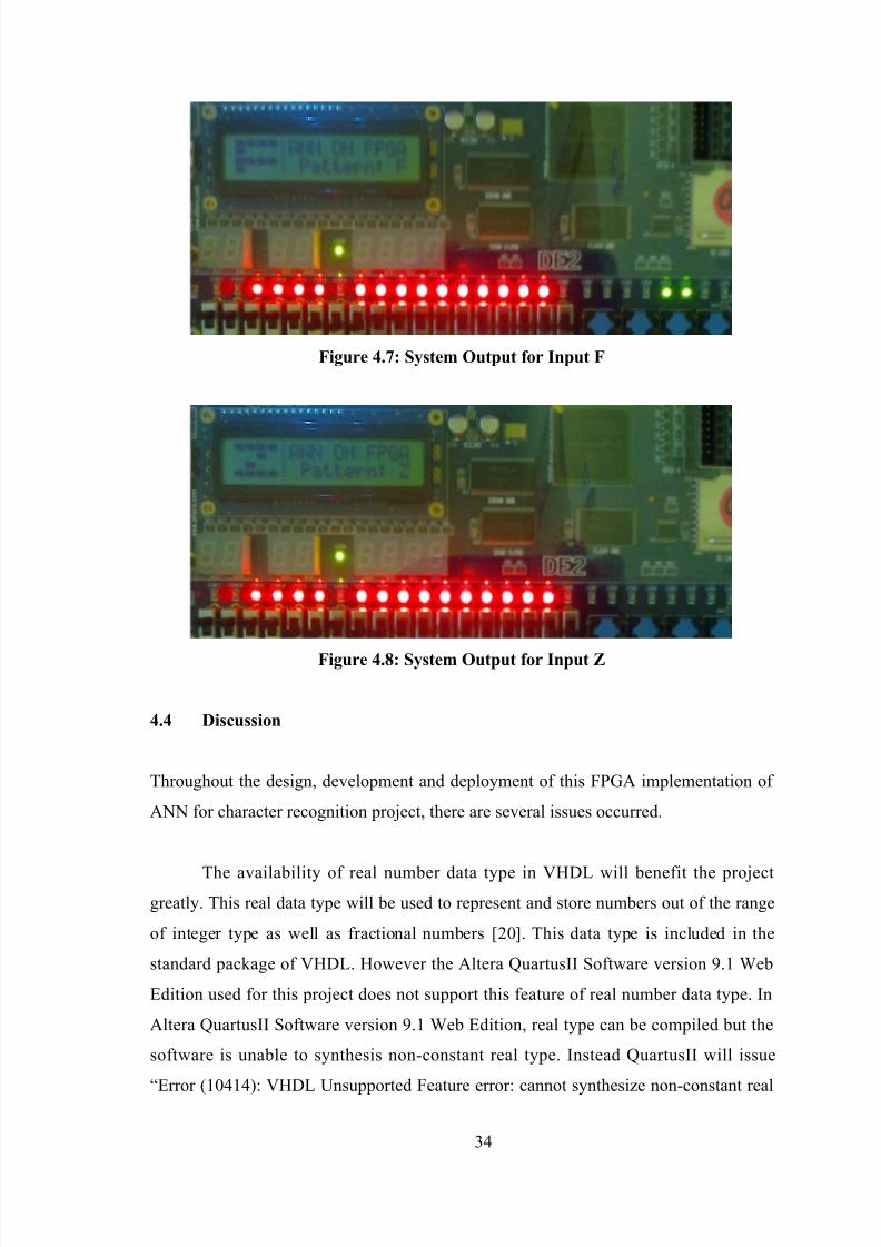
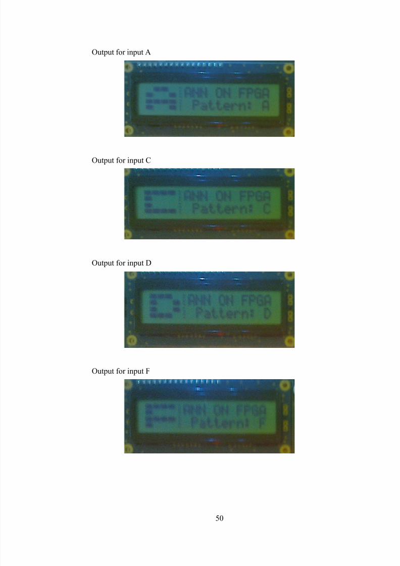
Figure 4.7: System Output for Input F
7/15/2019 EKT445/446 FYP report
http://slidepdf.com/reader/full/ekt445446-fyp-report 47/66
objects or values”. This issue had affected the project in many ways as real data types is
necessary to represent fractional and exponential numbers. The floating point processor
is used to overcome the issue in using VHDL real data type. Although Altera QuartusII
is unable to synthesis real numbers, the software does included a wizard to generate
files needed to process floating point values. This generated VHDL code for floating
point processing is used to process the fractional and exponential numbers exist in the
design of this project.
The connection weights in the ANN had to be initialised to random value of real
type when the ANN is reset. However due to above mentioned issue with real number
data type in Altera QuartusII, actual real type random number generator cannot be
modelled for this project. Moreover, it is hard to model an actual random number
generator in digital hardware. Therefore a pseudo-random number generator utilising
linear feedback shift-register is modelled to supplement the lack of real random number
generator in the design of this project.
The system is functioning properly and it is able to recognise the character
7/15/2019 EKT445/446 FYP report
http://slidepdf.com/reader/full/ekt445446-fyp-report 48/66
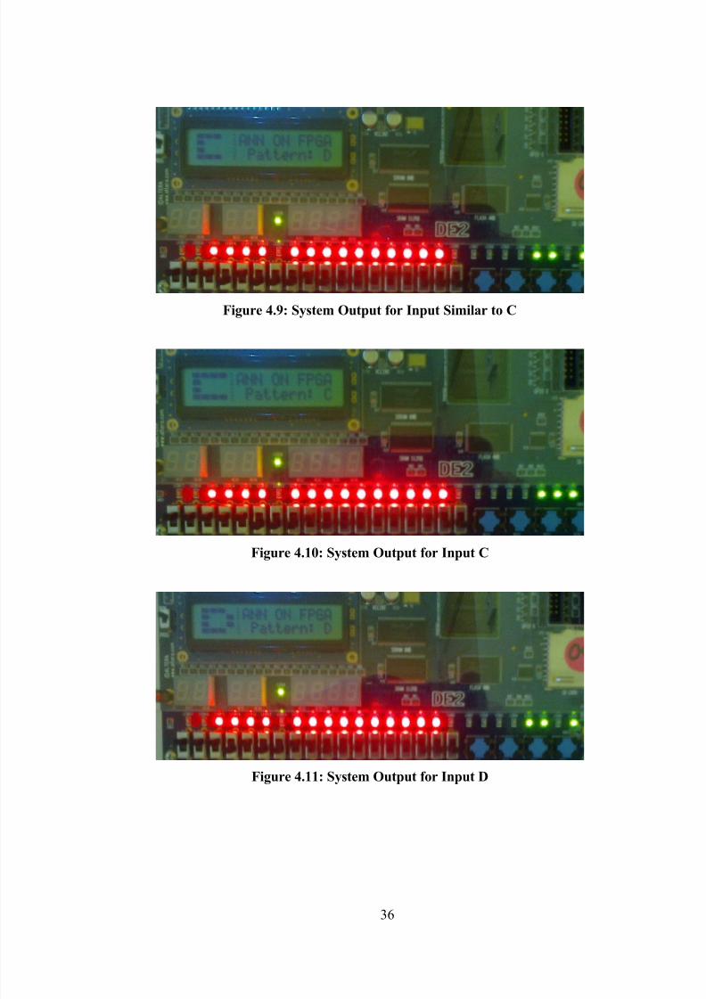
Figure 4.9: System Output for Input Similar to C
7/15/2019 EKT445/446 FYP report
http://slidepdf.com/reader/full/ekt445446-fyp-report 49/66
4.5 Conclusion
This project had produced favourable result. The system is capable to recognise all 16
character patterns included in its training data set. During initialisation, the system will
enter initialisation state before going to learning state where the ANN learn to recognise
the 16 character patterns in the training data set. During this time the system will not be
able to perform any recognition task until the ANN finishes the learning state. Users
input the character patterns into the system using SW17 – SW2 toggle switches on-
board the Altera DE2, and PB3 push-button switch is pressed to signal the ANN to
perform recognition process of the input character pattern. The input pattern and
recognition output is displayed on the LCD module. Apart from some issues discussed
earlier, this project is functional to recognise 16 character patterns.
7/15/2019 EKT445/446 FYP report
http://slidepdf.com/reader/full/ekt445446-fyp-report 50/66
CHAPTER 5
CONCLUSION
5.1 Introduction
This chapter of the report will include some concluding remarks regarding the project
and short discussion of possible future works to further improve the project.
5.2 Conclusion
7/15/2019 EKT445/446 FYP report
http://slidepdf.com/reader/full/ekt445446-fyp-report 51/66
In conclusion, this project works as an introduction to the endless possibilities of
ANN design, development and applications. This project is also an eye opener to the
infinite possibility of designing, developing and prototyping of new systems using
VHDL and FPGAs.
5.3 Future works
This project is by no means is finished. The ANN system developed for this project is
can be develop further to be able to recognise more character patterns with larger pixel
counts. The ANN may also be applied for other applications other than character
recognition, for example, voice recognition, natural image recognition, and many other
applications.
The VHDL code for this project can be further optimised to obtain better result
and performance. The issues discussed in Chapter 4 is yet to be solved. All of this
issues, optimisations, and developments regarding this project are just a small fraction
7/15/2019 EKT445/446 FYP report
http://slidepdf.com/reader/full/ekt445446-fyp-report 52/66
REFERENCES
[1] Gurney, K., (1997). An introduction to neural networks. London: UCL Press.
[2] Wikipedia, (2013). Neural network. Retrieved from en.wikipedia.org/wiki/
Neural_network
[3] EnchantedLearning.com, (2001). Brain cells. Retrieved from
http://www.enchantedlearning.com/subjects/anatomy/brain/Neuron.shtml
[4] Omandi, A. R., Rajapakse, J. C., & Bajger, M. (2006). FPGA neurocomputers. In A.
R. Omandi, & J. C. Rajapakse (Eds.), FPGA implementation of neural network (pp.
1-36). Netherlands: Springer.
[5] Wikibooks, (2008). Artificial neural networks/print version. Retrieved from
http://en.wikibooks.org/wiki/Artificial_Neural_Networks/Print_Version
[6] Satizábal, H., & Perez-Uribe, A., (2012). Supervised learning: TORCS, the open
racing car simulator. Retrieved from
http://ape.iict.ch/teaching/AIGS/AIGS_Labo/Labo4-Supervised
[7] Mol, A. C. D. A., Martinez, A. S., & Schirru, R. (2003). A neural model for transient
identification in dynamic processes with “don't know” response. Annals of Nuclear
7/15/2019 EKT445/446 FYP report
http://slidepdf.com/reader/full/ekt445446-fyp-report 53/66
[14] The Digital Electronics Blog, (2007). Comparison of VHDL to other hardware
description languages [Blog entry]. Retrieved from
http://digitalelectronics.blogspot.com/2007/07/comparison-of-vhdl-to-other-
hardware.html
[15] Altera Corporation, (n.d.). DE2 development and education board. Retrieved from
http://www.altera.com/education/univ/materials/boards/de2/unv-de2-board.html
[16] Terasic Technologies Inc., (n.d.). Altera DE2 board overview. Retrieved from
http://www.terasic.com.tw/cgi-bin/page/archive.pl?Language=English& Category
No=39&No=30
[17] Altera Corporation, (2012). DE2 development and education board user manual
[User manual] (Version 1.6). Altera Corporation.
[18] Terasic Technologies Inc., (n.d.). Altera DE2 board layout. Retrieved from
http://www.terasic.com.tw/attachment/archive/30/image/image_58_thumb.jpg
[19] Terasic Technologies Inc., (n.d.). Altera DE2 board kit content. Retrieved from
http://www.terasic.com.tw/cgi-bin/page/archive.pl?Language=English&Category
No=39&No=30&PartNo=5
[20] Perry, D. L., (2002). VHDL: Programming by example [4th ed.]. McGraw-Hill.
7/15/2019 EKT445/446 FYP report
http://slidepdf.com/reader/full/ekt445446-fyp-report 54/66
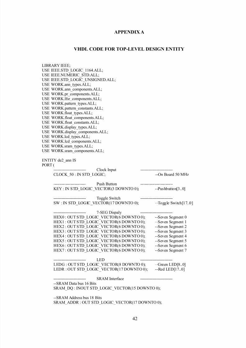
APPENDIX A
VHDL CODE FOR TOP-LEVEL DESIGN ENTITY
LIBRARY IEEE;
USE IEEE.STD_LOGIC_1164.ALL;USE IEEE.NUMERIC_STD.ALL;
USE IEEE.STD_LOGIC_UNSIGNED.ALL;
USE WORK.ann_types.ALL;
USE WORK.ann_components.ALL;USE WORK.pr_components.ALL;
USE WORK.lfsr_components.ALL;USE WORK.pattern_types.ALL;
USE WORK.pattern_constants.ALL;USE WORK.float_types.ALL;
USE WORK.float_components.ALL;USE WORK.float_constants.ALL;
USE WORK.display_types.ALL;
USE WORK.display_components.ALL;USE WORK.lcd_types.ALL;USE WORK.lcd_components.ALL;
USE WORK.sram_types.ALL;USE WORK.sram_components.ALL;
ENTITY de2_ann IS
PORT (------------------------ Clock Input ------------------------
7/15/2019 EKT445/446 FYP report
http://slidepdf.com/reader/full/ekt445446-fyp-report 55/66
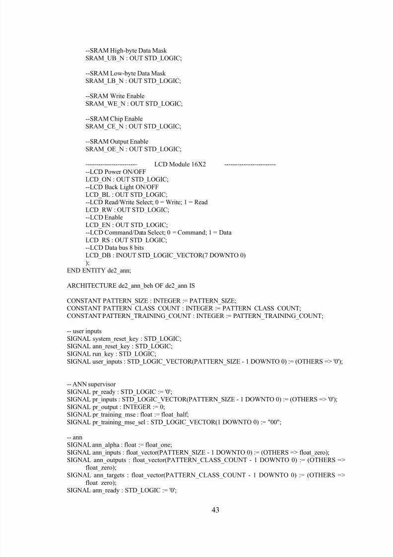
--SRAM High-byte Data Mask
SRAM_UB_N : OUT STD_LOGIC;
--SRAM Low-byte Data Mask SRAM_LB_N : OUT STD_LOGIC;
--SRAM Write Enable
SRAM_WE_N : OUT STD_LOGIC;
--SRAM Chip EnableSRAM_CE_N : OUT STD_LOGIC;
--SRAM Output EnableSRAM_OE_N : OUT STD_LOGIC;
------------------------ LCD Module 16X2 --------------------------LCD Power ON/OFF
LCD_ON : OUT STD_LOGIC;
--LCD Back Light ON/OFF
LCD_BL : OUT STD_LOGIC;--LCD Read/Write Select; 0 = Write; 1 = Read
LCD_RW : OUT STD_LOGIC;--LCD Enable
LCD_EN : OUT STD_LOGIC;--LCD Command/Data Select; 0 = Command; 1 = Data
LCD_RS : OUT STD_LOGIC;--LCD Data bus 8 bits
LCD_DB : INOUT STD_LOGIC_VECTOR(7 DOWNTO 0));
END ENTITY de2_ann;
7/15/2019 EKT445/446 FYP report
http://slidepdf.com/reader/full/ekt445446-fyp-report 56/66
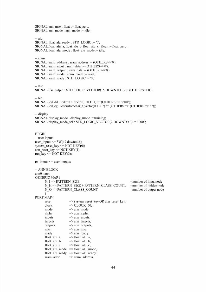
SIGNAL ann_mse : float := float_zero;
SIGNAL ann_mode : ann_mode := idle;
-- aluSIGNAL float_alu_ready : STD_LOGIC := '0';
SIGNAL float_alu_a, float_alu_b, float_alu_c : float := float_zero;SIGNAL float_alu_mode : float_alu_mode := idle;
-- sram
SIGNAL sram_address : sram_address := (OTHERS=>'0');SIGNAL sram_input : sram_data := (OTHERS=>'0');
SIGNAL sram_output : sram_data := (OTHERS=>'0');
SIGNAL sram_mode : sram_mode := read;SIGNAL sram_ready : STD_LOGIC := '0';
-- lfsr SIGNAL lfsr_output : STD_LOGIC_VECTOR(15 DOWNTO 0) := (OTHERS=>'0');
-- lcd
SIGNAL lcd_dd : lcdtext_t_vector(0 TO 31) := (OTHERS => x"00");SIGNAL lcd_cg : lcdcustomchar_t_vector(0 TO 7) := (OTHERS => (OTHERS => '0'));
-- display
SIGNAL display_mode : display_mode := training;SIGNAL display_mode_sel : STD_LOGIC_VECTOR(2 DOWNTO 0) := "000";
BEGIN-- user inputs
user_inputs <= SW(17 downto 2);
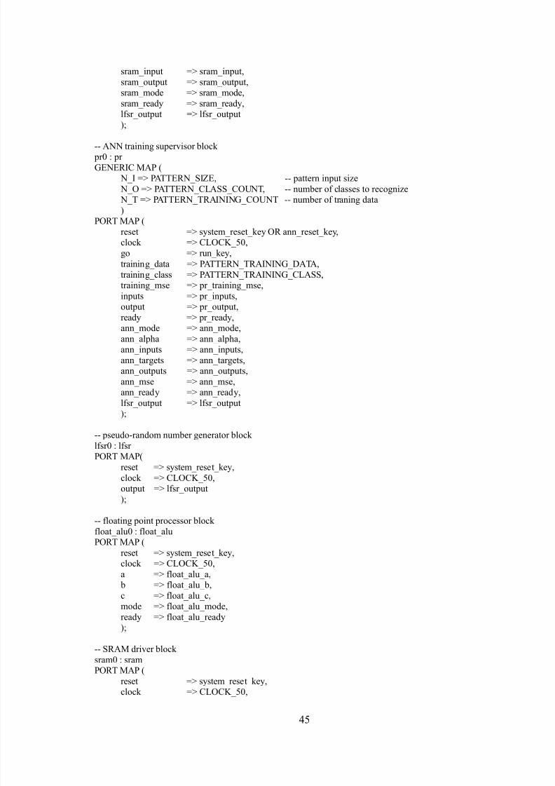
7/15/2019 EKT445/446 FYP report
http://slidepdf.com/reader/full/ekt445446-fyp-report 57/66
sram_input => sram_input,
sram_output => sram_output,sram_mode => sram_mode,
sram_ready => sram_ready,lfsr_output => lfsr_output
);
-- ANN training supervisor block pr0 : pr
GENERIC MAP ( N_I => PATTERN_SIZE, -- pattern input size
N_O => PATTERN_CLASS_COUNT, -- number of classes to recognize
N_T => PATTERN_TRAINING_COUNT -- number of traning data)
PORT MAP (
reset => system_reset_key OR ann_reset_key,clock => CLOCK_50,
go => run_key,
training_data => PATTERN_TRAINING_DATA,
training_class => PATTERN_TRAINING_CLASS,training_mse => pr_training_mse,
inputs => pr_inputs,output => pr_output,
ready => pr_ready,ann_mode => ann_mode,
ann_alpha => ann_alpha,ann_inputs => ann_inputs,
ann_targets => ann_targets,ann_outputs => ann_outputs,
ann_mse => ann_mse,
7/15/2019 EKT445/446 FYP report
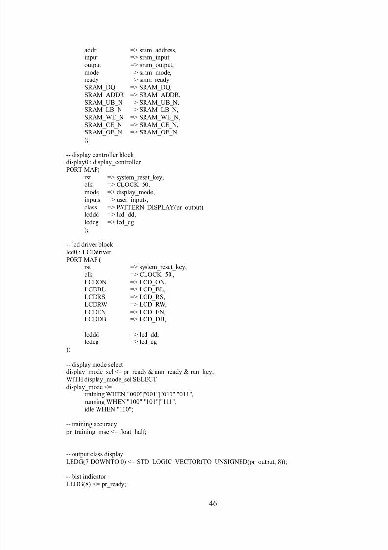
http://slidepdf.com/reader/full/ekt445446-fyp-report 58/66
addr => sram_address,
input => sram_input,output => sram_output,
mode => sram_mode,ready => sram_ready,
SRAM_DQ => SRAM_DQ,SRAM_ADDR => SRAM_ADDR,
SRAM_UB_N => SRAM_UB_N,SRAM_LB_N => SRAM_LB_N,
SRAM_WE_N => SRAM_WE_N,SRAM_CE_N => SRAM_CE_N,
SRAM_OE_N => SRAM_OE_N
);
-- display controller block
display0 : display_controller PORT MAP(
rst => system_reset_key,
clk => CLOCK_50,
mode => display_mode,inputs => user_inputs,
class => PATTERN_DISPLAY(pr_output),lcddd => lcd_dd,
lcdcg => lcd_cg);
-- lcd driver block
lcd0 : LCDdriver PORT MAP (
rst => system_reset_key,

7/15/2019 EKT445/446 FYP report
http://slidepdf.com/reader/full/ekt445446-fyp-report 59/66
-- mean squared error displayLEDR <= ann_mse(31 DOWNTO 14);
-- turn off the 7 segment displays
HEX0 <= (OTHERS => '1');HEX1 <= (OTHERS => '1');
HEX2 <= (OTHERS => '1');HEX3 <= (OTHERS => '1');
HEX4 <= (OTHERS => '1');HEX5 <= (OTHERS => '1');
HEX6 <= (OTHERS => '1');
HEX7 <= (OTHERS => '1');
END ARCHITECTURE de2_ann_beh;
7/15/2019 EKT445/446 FYP report
http://slidepdf.com/reader/full/ekt445446-fyp-report 60/66
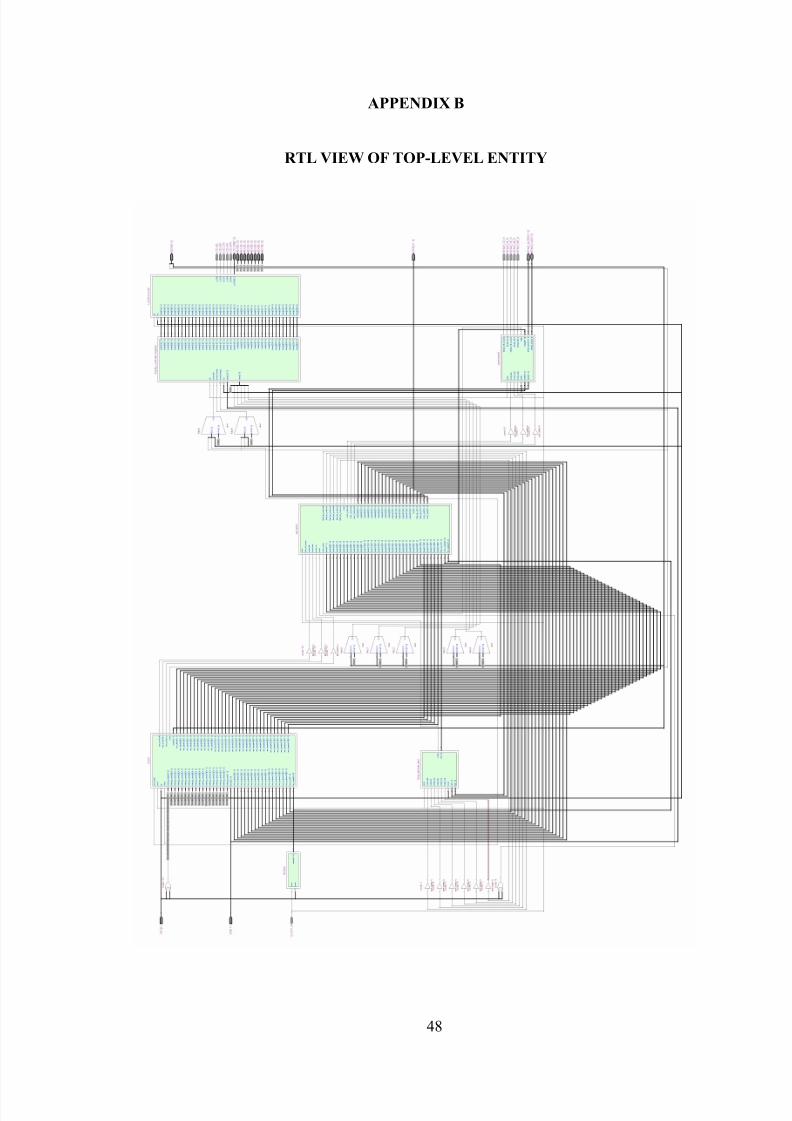
APPENDIX B
RTL VIEW OF TOP-LEVEL ENTITY
7/15/2019 EKT445/446 FYP report
http://slidepdf.com/reader/full/ekt445446-fyp-report 61/66
APPENDIX C
LCD OUTPUTS
During initialisation
When the ANN is training
7/15/2019 EKT445/446 FYP report
http://slidepdf.com/reader/full/ekt445446-fyp-report 62/66
Output for input A
Output for input C
Output for input D
7/15/2019 EKT445/446 FYP report
http://slidepdf.com/reader/full/ekt445446-fyp-report 63/66
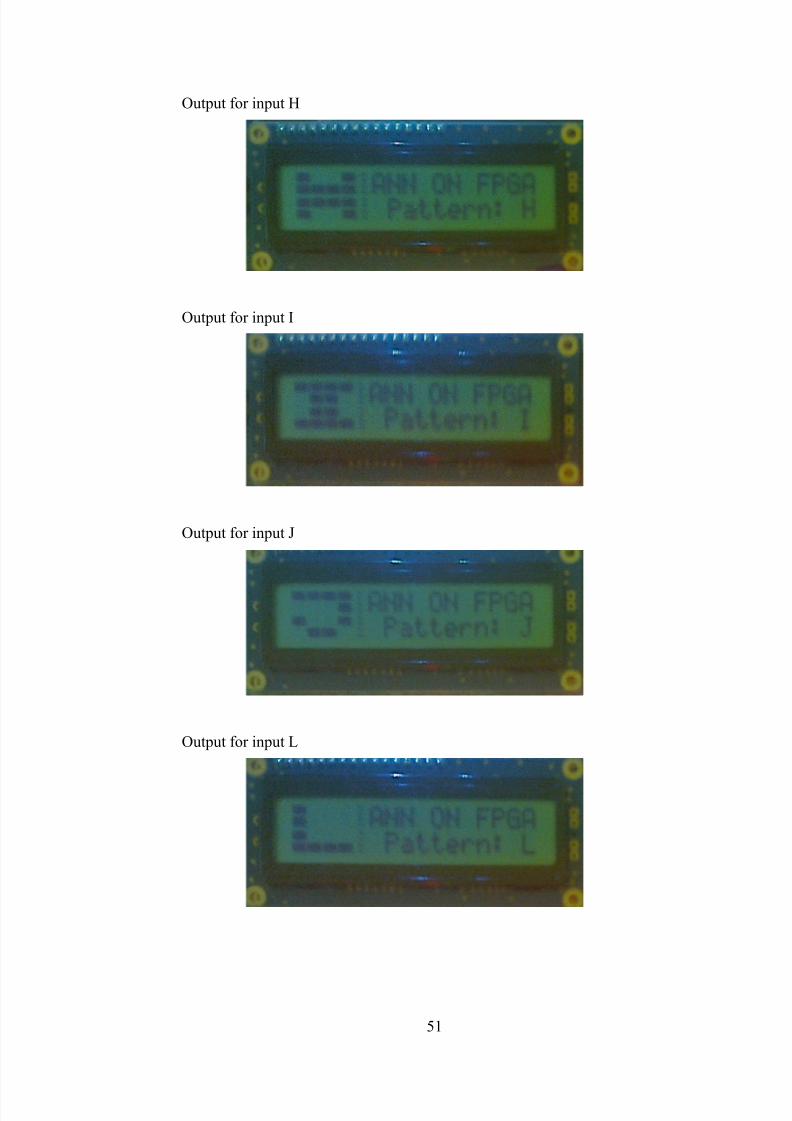
Output for input H
Output for input I
Output for input J
7/15/2019 EKT445/446 FYP report
http://slidepdf.com/reader/full/ekt445446-fyp-report 64/66
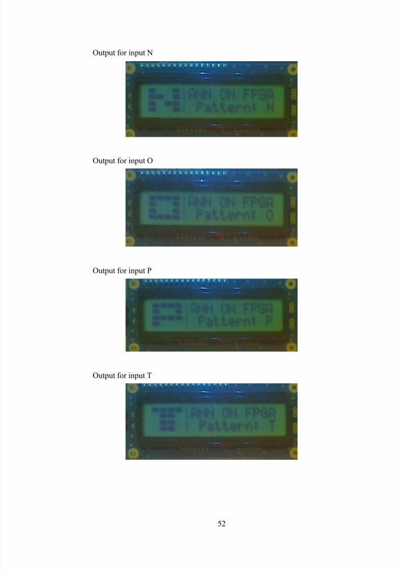
Output for input N
Output for input O
Output for input P
7/15/2019 EKT445/446 FYP report
http://slidepdf.com/reader/full/ekt445446-fyp-report 65/66
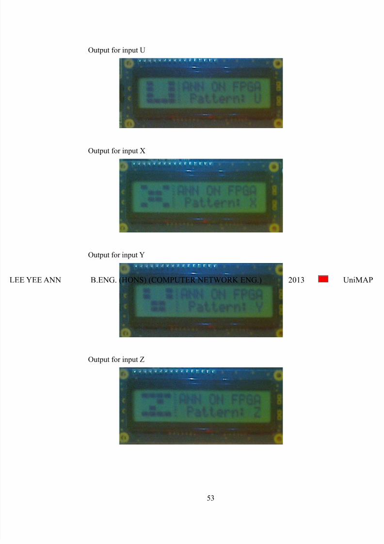
Output for input U
Output for input X
Output for input Y
LEE YEE ANN B.ENG. (HONS) (COMPUTER NETWORK ENG.) 2013 UniMAP

7/15/2019 EKT445/446 FYP report
http://slidepdf.com/reader/full/ekt445446-fyp-report 66/66