Embed Size (px)
Citation preview
J O U R N A L O F M A T E R I A L S S C I E N C E 3 9 (2 0 0 4 ) 4157 – 4170
Elastic and elastoplastic response
of thin copper foil
H. D. MERCHANTGould Electronics Inc., Eastlake, OH 44095, USA
G. KHATIBI, B. WEISS∗Inst. of Materialphysics, University of Vienna, Vienna, AustriaE-mail: [email protected]
The tensile elastic, elastoplastic and low strain plastic parameters of the 12–35 µm thickrolled (R) and electrodeposited (ED) copper foils have been characterized between 296 and573 K and after an anneal exposure at up to 1173 K. At 296 K, all parameters are inverselyproportional to grain size but the thermal effects dominate at the higher temperatures. Forthe R foils, the temperature coefficient of elastic modulus (E) is more or less identical tothat for the bulk copper. For the ED foils, the coefficient increases with decreasing grainsize; this effect is presumably related to the characteristic point defect structure generatedduring deposition. A significant grain growth ensues upon annealing but the post-annealgrain size has little effect on E; for the R foil, however, E decreases sharply with the annealinduced emergence of new crystallogrpahic textures with orientations near 〈100〉 . Thetangent modulus (Et) in the elastoplastic regime decreases with strain and withtemperature, a very large drop in Et with anneal temperature suggests that both thediminution of dislocation activity and the texture modification are the contributory factors.It is argued that the strain hardening parameter (n ) in the elastoplastic regime, and thestrain rate hardening parameter (m) and the flow stress in the low strain plastic regimeinfluence the handling damage to the thin foil. C© 2004 Kluwer Academic Publishers
1. IntroductionThe elastic response of thin film or foil has been in-vestigated by a variety of techniques: X-ray diffrac-tion [1–3], bending [4, 5] (cantilever beam [6], bi-axial[7], three-point [8]), indentation [9] (nano- [10], spher-ical tipped [11]), bulging [12, 13] sonics [14], elasticwaves [15], surface acoustics [16–18], vibrating reed[19, 20], dynamic mechanical analyzer (DMA) [21] andtensile loading [1, 22–25]. The most characterizations,however, have been at room temperature. The tensiletechnique, in particular, is amenable to tests at highertemperatures [23–25]; furthermore, it permits specificexamination of the elastoplastic (between proportionallimit and plastic yielding) and the low strain post-yieldresponses.
The freestanding copper foil has been investigatedin tensile mode to a limited extent [1, 22, 23, 25]. Thereported room temperature modulus values are oftenlower than those for the bulk copper [26]. The grainsize, the nature of grain boundaries, especially for thevapor or electrodeposited foil, and the incidence of mi-cropores and microcracks are prone to affect the modu-lus [15, 27]. The crystallographic texture, likewise, canhave a significant effect since the modulus of copper isdirection specific [28, 29]. For example, the modulus
∗Author to whom all correspondence should be addressed.
in the 〈111〉 direction is 2.9 times greater than that inthe 〈100〉 direction. The grain orientation as well as thegrain shape, in the as fabricated and annealed condi-tions, can influence the elastic modulus [30].
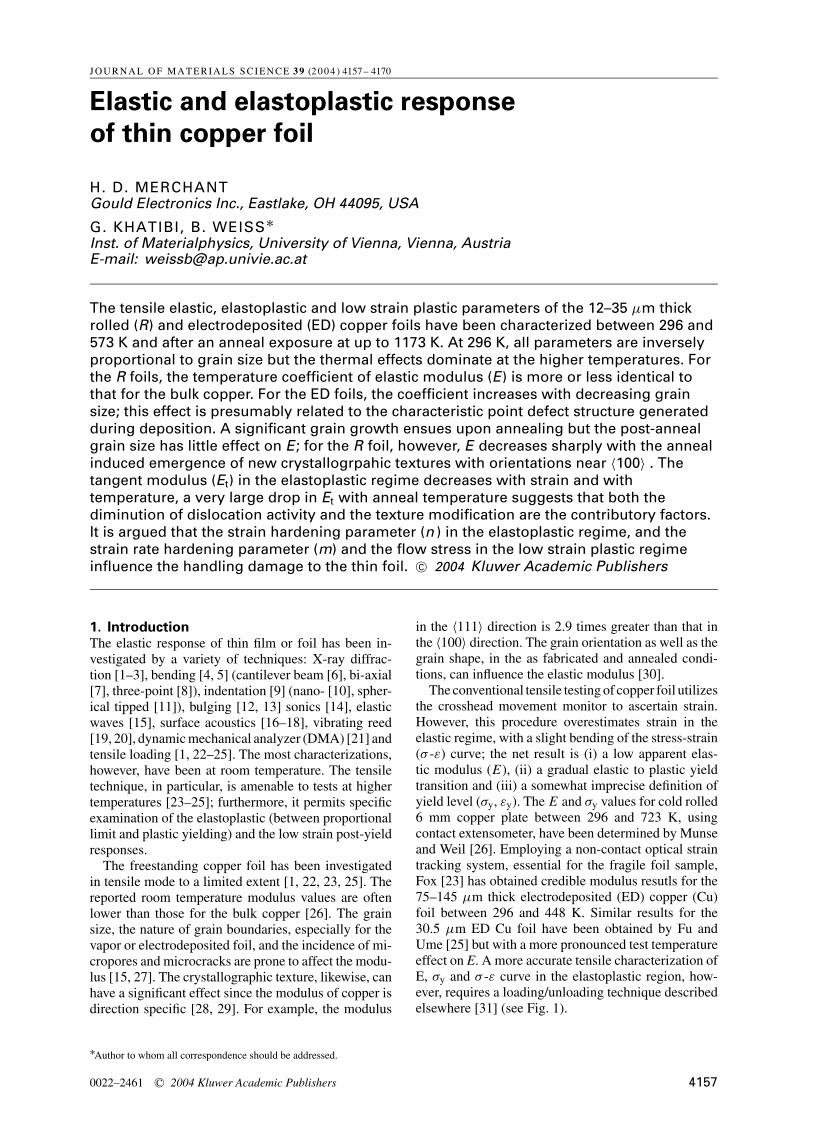
The conventional tensile testing of copper foil utilizesthe crosshead movement monitor to ascertain strain.However, this procedure overestimates strain in theelastic regime, with a slight bending of the stress-strain(σ -ε) curve; the net result is (i) a low apparent elas-tic modulus (E), (ii) a gradual elastic to plastic yieldtransition and (iii) a somewhat imprecise definition ofyield level (σy, εy). The E and σy values for cold rolled6 mm copper plate between 296 and 723 K, usingcontact extensometer, have been determined by Munseand Weil [26]. Employing a non-contact optical straintracking system, essential for the fragile foil sample,Fox [23] has obtained credible modulus resutls for the75–145 µm thick electrodeposited (ED) copper (Cu)foil between 296 and 448 K. Similar results for the30.5 µm ED Cu foil have been obtained by Fu andUme [25] but with a more pronounced test temperatureeffect on E. A more accurate tensile characterization ofE, σy and σ -ε curve in the elastoplastic region, how-ever, requires a loading/unloading technique describedelsewhere [31] (see Fig. 1).
0022–2461 C© 2004 Kluwer Academic Publishers 4157
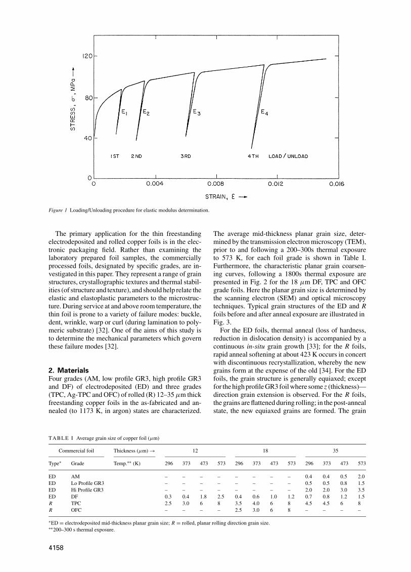
Figure 1 Loading/Unloading procedure for elastic modulus determination.
The primary application for the thin freestandingelectrodeposited and rolled copper foils is in the elec-tronic packaging field. Rather than examining thelaboratory prepared foil samples, the commerciallyprocessed foils, designated by specific grades, are in-vestigated in this paper. They represent a range of grainstructures, crystallographic textures and thermal stabil-ities (of structure and texture), and should help relate theelastic and elastoplastic parameters to the microstruc-ture. During service at and above room temperature, thethin foil is prone to a variety of failure modes: buckle,dent, wrinkle, warp or curl (during lamination to poly-meric substrate) [32]. One of the aims of this study isto determine the mechanical parameters which governthese failure modes [32].
2. MaterialsFour grades (AM, low profile GR3, high profile GR3and DF) of electrodeposited (ED) and three grades(TPC, Ag-TPC and OFC) of rolled (R) 12–35 µm thickfreestanding copper foils in the as-fabricated and an-nealed (to 1173 K, in argon) states are characterized.
T ABL E I Average grain size of copper foil (µm)
Commercial foil Thickness (µm) → 12 18 35
Type∗ Grade Temp.∗∗ (K) 296 373 473 573 296 373 473 573 296 373 473 573
ED AM – – – – – – – – 0.4 0.4 0.5 2.0ED Lo Profile GR3 – – – – – – – – 0.5 0.5 0.8 1.5ED Hi Profile GR3 – – – – – – – – 2.0 2.0 3.0 3.5ED DF 0.3 0.4 1.8 2.5 0.4 0.6 1.0 1.2 0.7 0.8 1.2 1.5R TPC 2.5 3.0 6 8 3.5 4.0 6 8 4.5 4.5 6 8R OFC – – – – 2.5 3.0 6 8 – – – –
∗ED = electrodeposited mid-thickness planar grain size; R = rolled, planar rolling direction grain size.∗∗200–300 s thermal exposure.
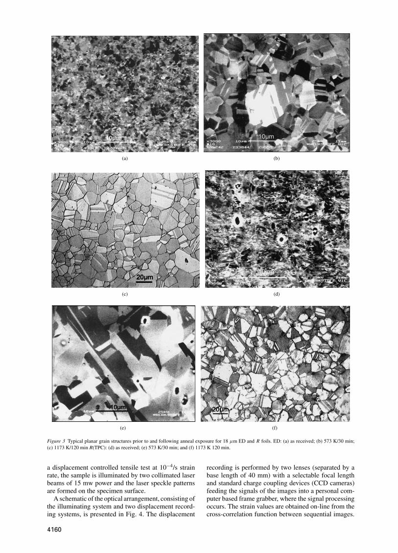
The average mid-thickness planar grain size, deter-mined by the transmission electron microscopy (TEM),prior to and following a 200–300s thermal exposureto 573 K, for each foil grade is shown in Table I.Furthermore, the characteristic planar grain coarsen-ing curves, following a 1800s thermal exposure arepresented in Fig. 2 for the 18 µm DF, TPC and OFCgrade foils. Here the planar grain size is determined bythe scanning electron (SEM) and optical microscopytechniques. Typical grain structures of the ED and Rfoils before and after anneal exposure are illustrated inFig. 3.
For the ED foils, thermal anneal (loss of hardness,reduction in dislocation density) is accompanied by acontinuous in-situ grain growth [33]; for the R foils,rapid anneal softening at about 423 K occurs in concertwith discontinuous recrystallization, whereby the newgrains form at the expense of the old [34]. For the EDfoils, the grain structure is generally equiaxed; exceptfor the high profile GR3 foil where some z (thickness)—direction grain extension is observed. For the R foils,the grains are flattened during rolling; in the post-annealstate, the new equiaxed grains are formed. The grain
4158
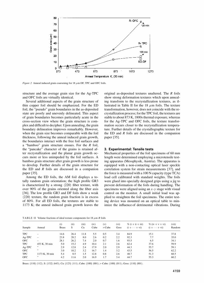
Figure 2 Anneal induced grain coarsening for 18 µm DF, TPC and OFC foils.
structure and the average grain size for the Ag-TPCand OFC foils are virtually identical.
Several additional aspects of the grain structure ofthin copper foil should be emphasized. For the EDfoil, the “pseudo” grain boundaries in the as-depositedstate are poorly and unevenly delineated. This aspectof grain boundaries becomes particularly acute in thecross-section view where the grain structure is com-plex and difficult to decipher. Upon annealing, the grainboundary delineation improves remarkably. However,when the grain size becomes comparable with the foilthickness, following the anneal induced grain growth,the boundaries interact with the free foil surfaces anda “bamboo” grain structure ensues. For the R foil,the “pancake” character of the grains is retained af-ter recrystallization and the planar grain growth oc-curs more or less unimpeded by the foil surfaces. Abamboo grain structure after grain growth is less proneto develop. Further details of the grain structure forthe ED and R foils are discussed in a companionpaper [35].
Among the ED foils, the AM foil displays a to-tally random grain orientation; the high profile GR3is characterized by a strong 〈220〉 fiber texture, withover 90% of the grains oriented along the fiber axis[36]. The low profile GR3 and DF foils show a weak〈220〉 texture, the random grain fraction is in excessof 80%. For all ED foils, the textures are stable to1173 K; the anneal induced grain growth leaves the
T ABL E I I Volume fractions of ideal texture components for 18 µm R foils
(i) (ii) (iii) (iv) (v) (vi) % (i + ii + iii) % (iv + v + vi) (vii)Sample Anneal Brass S Cu Cube r-Cube Goss (i + · · · + vi) (i + · · · + vi) Random
TPC – 14.6 26.4 11.8 5.5 0.5 3.4 84.9 15.1 37.8Ag-TPC – 23.8 28.2 8.0 2.6 0.2 2.2 92.3 7.7 35.0OFC – 28.1 26.2 7.4 2.0 0.7 1.6 93.5 6.5 34.1TPC 453 K, 30 min 5.0 15.2 4.9 10.4 2.1 2.6 62.4 37.6 59.9Ag-TPC ” 2.9 12.8 2.4 17.9 2.0 2.9 44.3 55.7 59.1OFC ” 3.0 10.2 3.2 16.7 1.4 3.2 43.5 56.5 62.2TPC 1173 K, 30 min 5.4 8.5 1.5 12.8 0.8 2.6 48.7 51.3 68.5OFC ” 4.2 11.6 2.0 16.9 1.7 3.4 44.7 55.3 60.2
Brass: {110} 〈112〉; S: {132} 〈643〉; Cu: {123} 〈111〉; Cube: {100} 〈001〉; r -Cube: {100} 〈011〉; Goss: {110} 〈001〉.
original as-deposited textures unaltered. The R foilsshow strong deformation textures which upon anneal-ing transform to the recrystallization textures, as il-lustrated in Table II for the 18 µm foils. The texturetransformation, however, does not coincide with the re-crystallization process; for the TPC foil, the textures arestable to about 873 K, 1800s thermal exposure, whereasfor the Ag-TPC and OFC foils, the texture transfor-mation occurs closer to the recrystallization tempera-ture. Further details of the crystallographic texture forthe ED and R foils are discussed in the companionpaper [35].
3. Experimental: Tensile testsMechanical properties of the foil specimens of 60 mmlength were determined employing a microtensile test-ing apparatus (Messphysik, Austria). The apparatus isequipped with a non-contacting optical laser specklecorrelation system for strain measurements [37], andthe force is measured with a 100 N capacity (type TCA)load cell calibrated with standard weights. The foilswere glued into specially designed grips using a jig toprevent deformation of the foils during handling. Thespecimens were aligned using an x-y stage with visualcontrol on the monitor. A small initial load was ap-plied to straighten the foil specimens. The entire test-ing device was mounted on an optical table to min-imize the influence of detrimental vibrations. During
4159
(a) (b)
(c) (d)
(e) (f)
Figure 3 Typical planar grain structures prior to and following anneal exposure for 18 µm ED and R foils. ED: (a) as received; (b) 573 K/30 min;(c) 1173 K/120 min R(TPC): (d) as received; (e) 573 K/30 min; and (f) 1173 K 120 min.
a displacement controlled tensile test at 10−4/s strainrate, the sample is illuminated by two collimated laserbeams of 15 mw power and the laser speckle patternsare formed on the specimen surface.
A schematic of the optical arrangement, consisting ofthe illuminating system and two displacement record-ing systems, is presented in Fig. 4. The displacement
recording is performed by two lenses (separated by abase length of 40 mm) with a selectable focal lengthand standard charge coupling devices (CCD cameras)feeding the signals of the images into a personal com-puter based frame grabber, where the signal processingoccurs. The strain values are obtained on-line from thecross-correlation function between sequential images.
4160
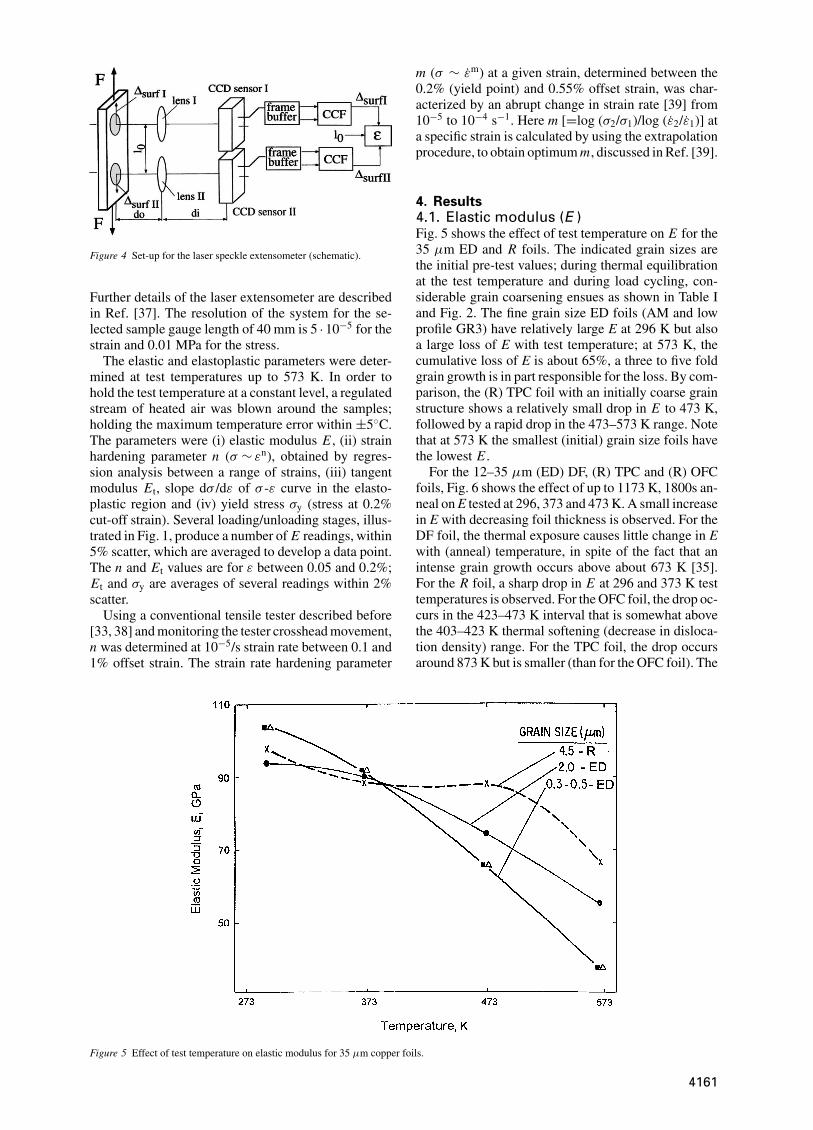
Figure 4 Set-up for the laser speckle extensometer (schematic).
Further details of the laser extensometer are describedin Ref. [37]. The resolution of the system for the se-lected sample gauge length of 40 mm is 5 · 10−5 for thestrain and 0.01 MPa for the stress.
The elastic and elastoplastic parameters were deter-mined at test temperatures up to 573 K. In order tohold the test temperature at a constant level, a regulatedstream of heated air was blown around the samples;holding the maximum temperature error within ±5◦C.The parameters were (i) elastic modulus E , (ii) strainhardening parameter n (σ ∼ εn), obtained by regres-sion analysis between a range of strains, (iii) tangentmodulus Et, slope dσ /dε of σ -ε curve in the elasto-plastic region and (iv) yield stress σy (stress at 0.2%cut-off strain). Several loading/unloading stages, illus-trated in Fig. 1, produce a number of E readings, within5% scatter, which are averaged to develop a data point.The n and Et values are for ε between 0.05 and 0.2%;Et and σy are averages of several readings within 2%scatter.
Using a conventional tensile tester described before[33, 38] and monitoring the tester crosshead movement,n was determined at 10−5/s strain rate between 0.1 and1% offset strain. The strain rate hardening parameter
Figure 5 Effect of test temperature on elastic modulus for 35 µm copper foils.
m (σ ∼ ε̇m) at a given strain, determined between the0.2% (yield point) and 0.55% offset strain, was char-acterized by an abrupt change in strain rate [39] from10−5 to 10−4 s−1. Here m [=log (σ2/σ1)/log (ε̇2/ε̇1)] ata specific strain is calculated by using the extrapolationprocedure, to obtain optimum m, discussed in Ref. [39].
4. Results4.1. Elastic modulus (E )Fig. 5 shows the effect of test temperature on E for the35 µm ED and R foils. The indicated grain sizes arethe initial pre-test values; during thermal equilibrationat the test temperature and during load cycling, con-siderable grain coarsening ensues as shown in Table Iand Fig. 2. The fine grain size ED foils (AM and lowprofile GR3) have relatively large E at 296 K but alsoa large loss of E with test temperature; at 573 K, thecumulative loss of E is about 65%, a three to five foldgrain growth is in part responsible for the loss. By com-parison, the (R) TPC foil with an initially coarse grainstructure shows a relatively small drop in E to 473 K,followed by a rapid drop in the 473–573 K range. Notethat at 573 K the smallest (initial) grain size foils havethe lowest E .
For the 12–35 µm (ED) DF, (R) TPC and (R) OFCfoils, Fig. 6 shows the effect of up to 1173 K, 1800s an-neal on E tested at 296, 373 and 473 K. A small increasein E with decreasing foil thickness is observed. For theDF foil, the thermal exposure causes little change in Ewith (anneal) temperature, in spite of the fact that anintense grain growth occurs above about 673 K [35].For the R foil, a sharp drop in E at 296 and 373 K testtemperatures is observed. For the OFC foil, the drop oc-curs in the 423–473 K interval that is somewhat abovethe 403–423 K thermal softening (decrease in disloca-tion density) range. For the TPC foil, the drop occursaround 873 K but is smaller (than for the OFC foil). The
4161
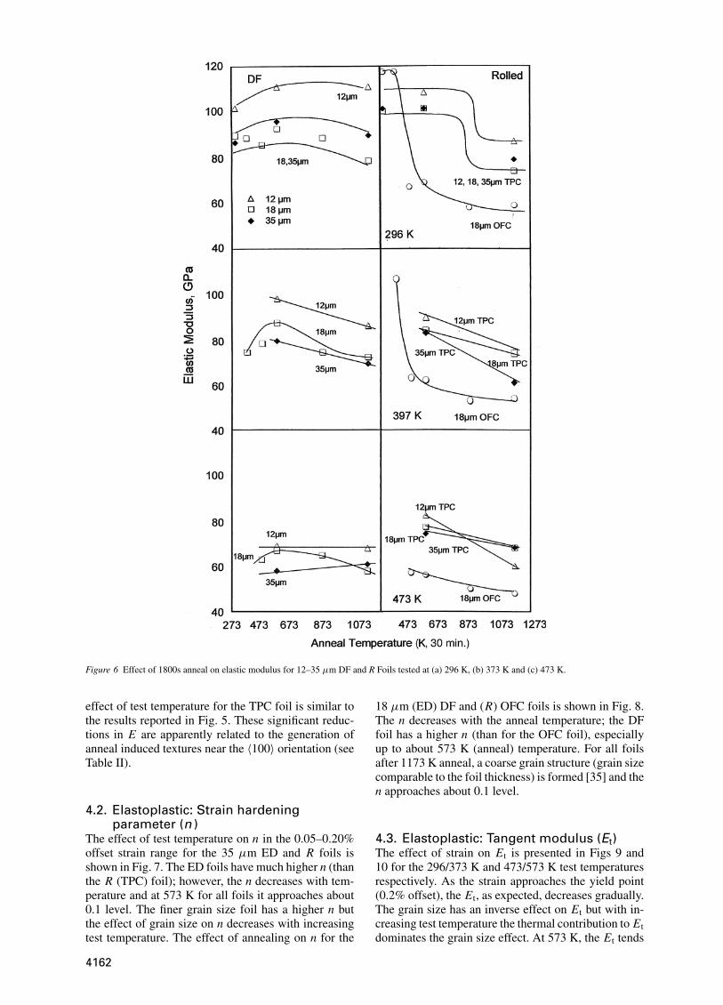
Figure 6 Effect of 1800s anneal on elastic modulus for 12–35 µm DF and R Foils tested at (a) 296 K, (b) 373 K and (c) 473 K.
effect of test temperature for the TPC foil is similar tothe results reported in Fig. 5. These significant reduc-tions in E are apparently related to the generation ofanneal induced textures near the 〈100〉 orientation (seeTable II).
4.2. Elastoplastic: Strain hardeningparameter (n )
The effect of test temperature on n in the 0.05–0.20%offset strain range for the 35 µm ED and R foils isshown in Fig. 7. The ED foils have much higher n (thanthe R (TPC) foil); however, the n decreases with tem-perature and at 573 K for all foils it approaches about0.1 level. The finer grain size foil has a higher n butthe effect of grain size on n decreases with increasingtest temperature. The effect of annealing on n for the
18 µm (ED) DF and (R) OFC foils is shown in Fig. 8.The n decreases with the anneal temperature; the DFfoil has a higher n (than for the OFC foil), especiallyup to about 573 K (anneal) temperature. For all foilsafter 1173 K anneal, a coarse grain structure (grain sizecomparable to the foil thickness) is formed [35] and then approaches about 0.1 level.
4.3. Elastoplastic: Tangent modulus (Et)The effect of strain on Et is presented in Figs 9 and10 for the 296/373 K and 473/573 K test temperaturesrespectively. As the strain approaches the yield point(0.2% offset), the Et, as expected, decreases gradually.The grain size has an inverse effect on Et but with in-creasing test temperature the thermal contribution to Etdominates the grain size effect. At 573 K, the Et tends
4162
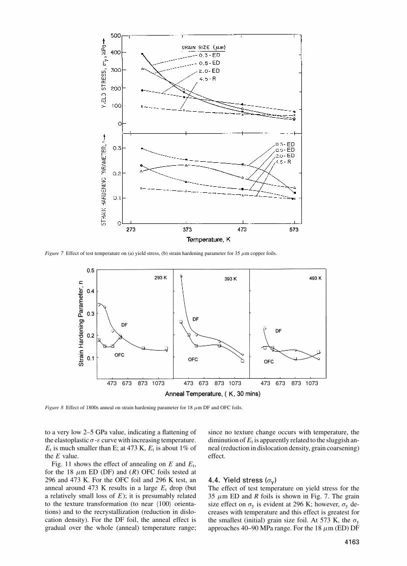
Figure 7 Effect of test temperature on (a) yield stress, (b) strain hardening parameter for 35 µm copper foils.
Figure 8 Effect of 1800s anneal on strain hardening parameter for 18 µm DF and OFC foils.
to a very low 2–5 GPa value, indicating a flattening ofthe elastoplastic σ -ε curve with increasing temperature.Et is much smaller than E; at 473 K, Et is about 1% ofthe E value.
Fig. 11 shows the effect of annealing on E and Et,for the 18 µm ED (DF) and (R) OFC foils tested at296 and 473 K. For the OFC foil and 296 K test, ananneal around 473 K results in a large Et drop (buta relatively small loss of E); it is presumably relatedto the texture transformation (to near 〈100〉 orienta-tions) and to the recrystallization (reduction in dislo-cation density). For the DF foil, the anneal effect isgradual over the whole (anneal) temperature range;
since no texture change occurs with temperature, thediminution of Et is apparently related to the sluggish an-neal (reduction in dislocation density, grain coarsening)effect.
4.4. Yield stress (σy)The effect of test temperature on yield stress for the35 µm ED and R foils is shown in Fig. 7. The grainsize effect on σy is evident at 296 K; however, σy de-creases with temperature and this effect is greatest forthe smallest (initial) grain size foil. At 573 K, the σyapproaches 40–90 MPa range. For the 18 µm (ED) DF
4163
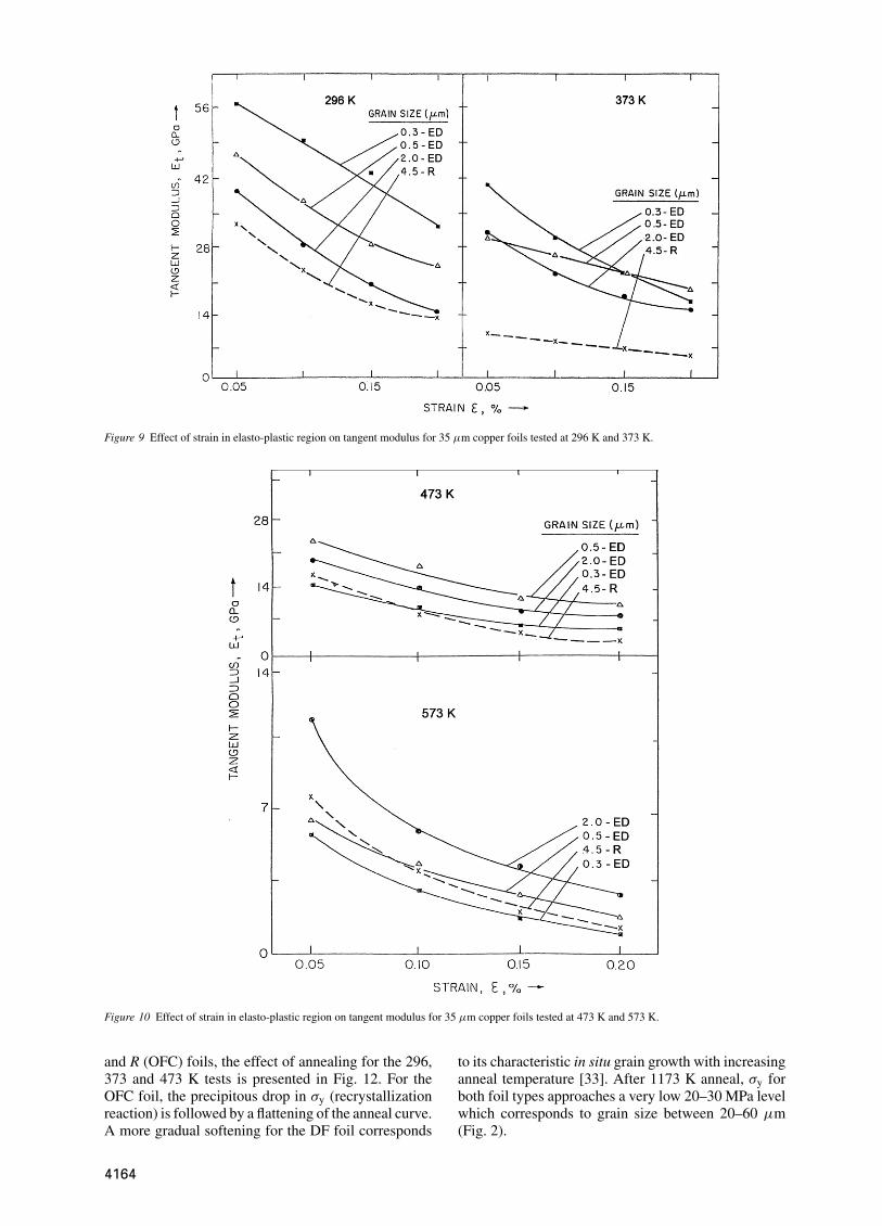
Figure 9 Effect of strain in elasto-plastic region on tangent modulus for 35 µm copper foils tested at 296 K and 373 K.
Figure 10 Effect of strain in elasto-plastic region on tangent modulus for 35 µm copper foils tested at 473 K and 573 K.
and R (OFC) foils, the effect of annealing for the 296,373 and 473 K tests is presented in Fig. 12. For theOFC foil, the precipitous drop in σy (recrystallizationreaction) is followed by a flattening of the anneal curve.A more gradual softening for the DF foil corresponds
to its characteristic in situ grain growth with increasinganneal temperature [33]. After 1173 K anneal, σy forboth foil types approaches a very low 20–30 MPa levelwhich corresponds to grain size between 20–60 µm(Fig. 2).
4164
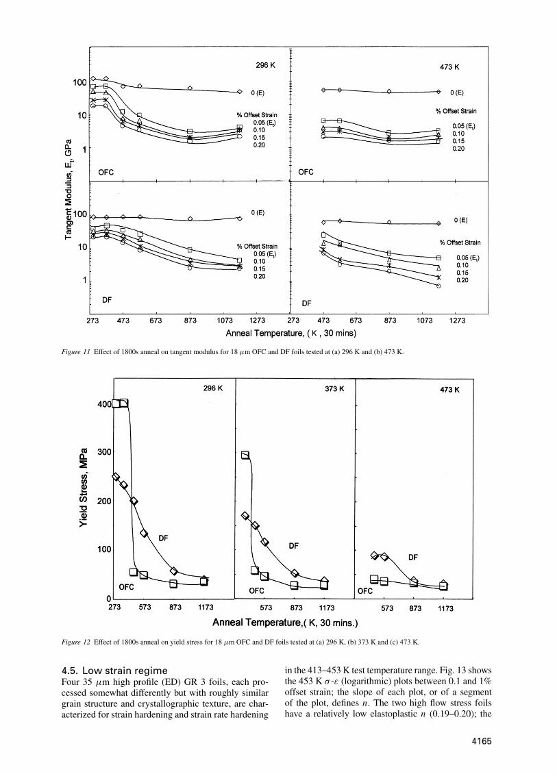
Figure 11 Effect of 1800s anneal on tangent modulus for 18 µm OFC and DF foils tested at (a) 296 K and (b) 473 K.
Figure 12 Effect of 1800s anneal on yield stress for 18 µm OFC and DF foils tested at (a) 296 K, (b) 373 K and (c) 473 K.
4.5. Low strain regimeFour 35 µm high profile (ED) GR 3 foils, each pro-cessed somewhat differently but with roughly similargrain structure and crystallographic texture, are char-acterized for strain hardening and strain rate hardening
in the 413–453 K test temperature range. Fig. 13 showsthe 453 K σ -ε (logarithmic) plots between 0.1 and 1%offset strain; the slope of each plot, or of a segmentof the plot, defines n. The two high flow stress foilshave a relatively low elastoplastic n (0.19–0.20); the
4165
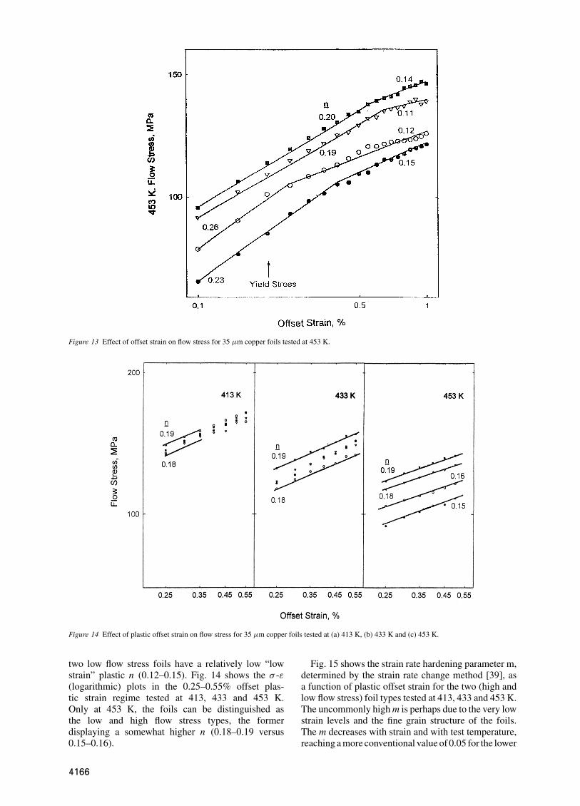
Figure 13 Effect of offset strain on flow stress for 35 µm copper foils tested at 453 K.
Figure 14 Effect of plastic offset strain on flow stress for 35 µm copper foils tested at (a) 413 K, (b) 433 K and (c) 453 K.
two low flow stress foils have a relatively low “lowstrain” plastic n (0.12–0.15). Fig. 14 shows the σ -ε(logarithmic) plots in the 0.25–0.55% offset plas-tic strain regime tested at 413, 433 and 453 K.Only at 453 K, the foils can be distinguished asthe low and high flow stress types, the formerdisplaying a somewhat higher n (0.18–0.19 versus0.15–0.16).
Fig. 15 shows the strain rate hardening parameter m,determined by the strain rate change method [39], asa function of plastic offset strain for the two (high andlow flow stress) foil types tested at 413, 433 and 453 K.The uncommonly high m is perhaps due to the very lowstrain levels and the fine grain structure of the foils.The m decreases with strain and with test temperature,reaching a more conventional value of 0.05 for the lower
4166
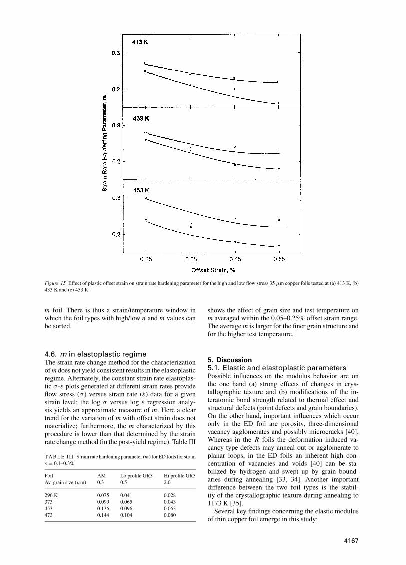
Figure 15 Effect of plastic offset strain on strain rate hardening parameter for the high and low flow stress 35 µm copper foils tested at (a) 413 K, (b)433 K and (c) 453 K.
m foil. There is thus a strain/temperature window inwhich the foil types with high/low n and m values canbe sorted.
4.6. m in elastoplastic regimeThe strain rate change method for the characterizationof m does not yield consistent results in the elastoplasticregime. Alternately, the constant strain rate elastoplas-tic σ -ε plots generated at different strain rates provideflow stress (σ ) versus strain rate (ε̇) data for a givenstrain level; the log σ versus log ε̇ regression analy-sis yields an approximate measure of m. Here a cleartrend for the variation of m with offset strain does notmaterialize; furthermore, the m characterized by thisprocedure is lower than that determined by the strainrate change method (in the post-yield regime). Table III
T ABL E I I I Strain rate hardening parameter (m) for ED foils for strainε = 0.1–0.3%
Foil AM Lo profile GR3 Hi profile GR3Av. grain size (µm) 0.3 0.5 2.0
296 K 0.075 0.041 0.028373 0.099 0.065 0.043453 0.136 0.096 0.063473 0.144 0.104 0.080
shows the effect of grain size and test temperature onm averaged within the 0.05–0.25% offset strain range.The average m is larger for the finer grain structure andfor the higher test temperature.
5. Discussion5.1. Elastic and elastoplastic parametersPossible influences on the modulus behavior are onthe one hand (a) strong effects of changes in crys-tallographic texture and (b) modifications of the in-teratomic bond strength related to thermal effect andstructural defects (point defects and grain boundaries).On the other hand, important influences which occuronly in the ED foil are porosity, three-dimensionalvacancy agglomerates and possibly microcracks [40].Whereas in the R foils the deformation induced va-cancy type defects may anneal out or agglomerate toplanar loops, in the ED foils an inherent high con-centration of vacancies and voids [40] can be sta-bilized by hydrogen and swept up by grain bound-aries during annealing [33, 34]. Another importantdifference between the two foil types is the stabil-ity of the crystallographic texture during annealing to1173 K [35].
Several key findings concerning the elastic modulusof thin copper foil emerge in this study:
4167
(i) Modulus for the R (TPC) foil is somewhat belowthat for the bulk polycrystalline copper [26] but it issignificantly greater than that for the ED foils (Fig. 5).
(ii) The modest test temperature effect on modulusfor the R (TPC) foil up to 573 K (Fig. 5) is similar to thatfor the bulk copper [26] but the effect is much smallerthan that for the ED foils.
(iii) Annealing the R (TPC) foil to 873 K or the EDfoils to 1173 K has little effect on modulus (Fig. 6) sinceneither foil type undergoes a texture transformation dur-ing thermal softening (modification of grain structure,reduction in dislocation density) or during subsequentgrain growth.
(iv) The constancy of modulus with anneal temper-ature up to 873 K for the R (TPC), tough pitch cop-per, foil is apparently related to the 300–400 ppm oxy-gen present in the form of oxide particulates [35]. Ifthe oxygen is reduced to less than 25 ppm, as forthe (R) OFC foil, or if a few hundred ppm Ag isadded to the R (TPC), as for the (R) Ag-TPC foil,the annealing has a considerable modulus loweringeffect.
(v) A precipitous drop in modulus at temperaturesabove the anneal softening temperature for the R (OFC)and R (TPC) foils (Fig. 6), near 473 and 873 K respec-tively, is related to the crystallographic texture trans-formation to orientations near 〈100〉.
(vi) Since the anneal induced grain coarsening doesnot result in a significant modulus change (Fig. 6),the grain size effect on 23◦C modulus and on tem-perature coefficient of modulus, as for the ED foils(Fig. 5), may be related to the deposition processinggenerated point defects “fingerprint” left in the foil[40], rather than to the grain size per se. However,the secondary effect of grain size on modulus is notdiscounted.
Indeed, the grain size affects the room temperature val-ues of E (Fig. 5), σy and n (Fig. 7), Et (Fig. 9) andm (Table III); the smaller grain size corresponds to thehigher values for all parameters. Above 296 K, the ther-mal (test or anneal temperature) effects begin to dom-inate the grain size contribution. A large change in E ,often over a relatively narrow range of temperatures,suggests a texture transformation (Fig. 6) whereas alarge change in σy suggests a reduction in dislocationdensity (Fig. 12). The elastoplastic parameters n (Fig. 8)and Et (Fig. 11) are influenced by a change in textureas well as in dislocation density, their relative contribu-tion depending upon the strain level, and to a less extentby the modification of grain structure. For example, alarge drop in Et around 473 K for the OFC foil (Fig. 11)is apparently due to recrystallization as well as dueto texture modification. An enhanced change of grainsize for the ED samples with the smallest grain size(0.3 µm) is apparently responsible for the extraordinarydrop in Et with anneal temperature (Figs 9 and 10). Theflow stress (Figs 13 and 14), m (Table III, Fig. 15) andn (Fig. 8) are postulated, as discussed in the follow-ing section, to relate to handling damage of the thinfoil.
5.2. Relation to handling damageThe major use of thin copper foil is in the manufac-ture of printed circuit (wiring) board; the foil is lam-inated to the polymeric substrate (FR-4, polyimide)and is further processed (circuitization of conductorlayer, lamination of cover layer, solder reflow), of-ten at temperatures in excess of 413 K. The foil isprone to handling damage such as wrinkling, (im-pact) denting and micro-buckling at or above roomtemperature. The laminate, if improperly designed orprocessed, is prone to (particulate) denting and z-direction distortion such as warpage and curl duringlamination (413–473 K) or during further processing(373–573 K).
Under the conditions of non-uniform loading, smallscale wrinkles, buckles or dents initiate near the straingradients at selected points on the foil [41]. At thesepoints of instability, an elastic or elastoplastic collapseis brought on by the in-plane compressive stress [42].The beneficial effects of σy (or flow stress), n and min circumventing the localized small scale visible de-fects has been recognized [43, 44]. High σy or flowstress guarantees elastic recovery of defects or reducesthe plastic strain; high E and Et enhance the wrinklemodulus and hence the critical stress for initiating themicrodefects [45]; high n results in a broader, moreuniform distribution of strain in the presence of a stressgradient [46]; high m aids in resisting strain localiationduring the development of instability [46]. An increasein n decreases the pre-instability (elastoplastic) straingradients whereas an enhanced m decreases the post-instability (low strain plastic) strain gradients [47]. Inparticular, the role of m in retarding the growth of insta-bility becomes greater as the foil thickness decreases[48, 49].
The thermal expansion differential between copperand substrate is the driver for distortion defects in thelaminates and the multi-layer stacks. Given this differ-ential, the extent of warp or curl depends upon ther-mal loading (temperature cycle, thermal stress), stackgeometry, process controls and E , Et for copper andsubstrate [32]. The warpage may occur during (i) lam-ination, (ii) circuitization of the copper layer by etch-ing, (iii) reflow or infrared soldering and (iv) soldermasking process. The three-dimensional thermoelas-tic or thermoviscoelastic models have been formulated[50] for a measure of warp and as an aid to laminatedesign. In the event of high thermal loading, Et maybe substituted for E but the viscoelastic or plastic re-laxation (the reduction of thermal stresses) may occurat the peak lamination or soldering temperature, con-siderably complicating the analysis. The finite elementanalysis (FEA) models [51–53] effectively handle thecomplex design and processing details, and provide amore reliable quantitative measure of distortion and thecause/effect understanding of the underlying factors.Both the analytical and FEA modeling require “good”mechanical and thermal parameters and their tempera-ture dependency, which we have shown in this study tobe unique to each foil type.
This study is the pioneering effort in characterizingthe mechanical parameters for the thin R and ED copper
4168
foils over a range of temperatures of interest. Also un-derway is the measurement of thermal expansion be-havior of the R and ED copper foils over a range oftemperatures. These results will be reported in the nearfuture.
6. Conclusions(i) Elastic Regime: At 296 K, the E is inversely pro-
portional to the grain size. For the R foil, the temper-ature dependency of E is similar to that for the bulkcopper. For the ED foil, the temperature dependency isgreater (than for the R foil) and it increases with thedecreasing initial grain size; this grain size effect is as-sumed to be due to the point defects fingerprint uniqueto each ED foil. The post-anneal grain size has a rela-tively small effect on E except for the R foils where theanneal induced emergence of crystallographic texturesnear the 〈100〉 orientation results in a sharp drop in E;for the TPC foil the drop is near 873 K and for the OFCfoil it is near 473 K. The foil thickness has a small effecton E.
(ii) Elastoplastic Regime: At 296 K, the values ofEt, σy, n and m are inversely proportional to the grainsize; at higher temperatures, this grain size effect isdominated by the thermal effects. At 573 K, the foilshave close σy and n, irrespective of the grain size. Bothσy and n decrease with temperature; the drop in σy,due to the diminution of dislocation activity, is abruptfor the R foil and gradual over a wide range of annealtemperatures for the DF foil. The Et decreases withstrain and with temperature; this temperature effect onEt is much greater than that on E. For the OFC foil,a large drop in Et around 473 K is apparently due torecrystallization as well as due to texture modification.The m increases mildly with the test temperature.(iii) Low Strain Plastic Regime: The m values for thin
ED foils are significantly higher than those reported forthe sheet in the higher strain regime; m decreases withstrain and increases mildly with the test temperature.The flow stress, m and n, are postulated to relate to thehandling damage of the thin foil.
AcknowledgementsR. Wiechmann (Gould) engaged the authors in stim-ulating and helpful discussions during various stagesof this investigation. E. El-Magd performed the me-chanical testing with the micro-tensile tester. M. Minor(Gould) performed the crosshead monitor tests in thelow strain plastic regime and conducted the carefuldata analysis of all results. For partial financial assis-tance for one author (G. Khatibi), we like to thankthe Austrian National Science Foundation, ProjectNo. 14732 TEC.
References1. M. Y. F U K S, L . S . P A L A T N I K, A. I . I L I N S K I I and V.
V. B E L O Z E R O V , Sov. Phys.—Solid State 9(3) (1967) 588.2. H . A S A D A, Y. K I S H I and Y. H I R O S E , Thin Solid Films 236
(1993) 247.3. M. E L E N A et al., ibid. 236 (1993) 209.
4. J . A . S C H W E I T Z , MRS Bulletin 7 (1992) 34.5. G . C . B R O W N and R. J . P R Y P U T N I E W I C Z , Proc. SPIE
2004 (1993) 304.6. J . M E N C I K, E . Q U A N D T and D. M U N Z , Thin Solid Films
287 (1996) 208.7. A . K . J A M T I N G, J . M. B E L L, M. V. S W A I N and N.
S C H W A R Z E R , ibid. 308/309 (1997) 304.8. A . R O U Z A U D, E . B A R B I E R, J . E M O U L T and E .
Q U E S N E L , ibid. 270 (1995) 270.9. M. F . D O E R N E R and W. D. N I X , J. Mater. Res. 1 (1986) 601.
10. D . S O N, Y. H. L E E , J . H . A H N and D. K W O N , in MRSSymp. Poc., Polycrystalline Metals and Magnetic Thin Films (1999)Vol. 562, p. 201.
11. M. V. S W A I N and J . M E N C I K , Thin Solid Films 253 (1994)204.
12. S . J A Y A R A M A N, R. L . E D W A R D S and K. J . H E M K E R ,in MRS Symp. Proc., Thin Films—Stresses and Mechanical Prop-erties (1998) Vol. 505, p. 623.
13. A . J . K A L K M A N, A. H. V E R G R U G G E N, G. C . A .M. J A N S S E N and F .H . G R O E N , Rev. Sci. Instr. 70 (1999)4026.
14. H . J . R E A D and A. H. G R A H A M , J. Electrochem. Soc. 108(1961) 73.
15. V . V . P O L Y A K O V and A. V. G O L O V I N , Russian Met. (4)(1995) 81.
16. A . N E U B R A N D and P . H E S S , J. Appl. Phys. 71 (1992) 227.17. B . S C H U L T R I C H et al., Thin Solid Films 253 (1994) 125.18. H . C O U F A L et al., J. Phys. III (Paris) Colloq. C 74 (1994) 717.19. H . M I Z U B A Y A S H I , Y . Y O S H I H A R A and S . O K U D A ,
Phys. Stat. Sol. (a) 129 (1992) 475.20. H . M I Z U B A Y A S H I , T . Y A M A G U C H I and Y.
Y O S H I H A R A , J. Alloys Compounds 211/212 (1994) 446.21. J . O . S K I , K . H . W U and G. L A R K I N S , Mater. Charac. 38
(1997) 301.22. V . A . L A M B, C. E . J O H N S O N and D. R . V A L E N T I N E ,
J. Electrochem. Soc. 117 (1970) 291C; 341C; 381C.23. A . F O X , J. Testing Evaluation 4 (1976) 74.24. G . T . M E A R I N I and R. W. H O F F M A N , J. Electronic Mats.
22 (1993) 623.25. C . Y . F U and C. U M E , JOM 47(6) (1995) 31.26. W. H. M U N S E and N. A. W E I L , ASTM Proc. 51 (1951) 996.27. V . K R S T I C , U . E R B and G. P A L U M B O , Scr. Metall. Mater.
29 (1993) 1501.28. W. C . O V E R T O N, J R . and J . G A F F N E Y , Phys. Rev. 98 (1997)
969.29. J . H . C H O I , S . Y . K A N G and D. Y. L E E , J. Mater. Sci. 35
(2000) 4055.30. B . C . H E N D R I X, L . G . Y U, K. W. X U and J . W. H E ,
MRS Symp. Proc., Polycrystalline Thin Films: Structure, Texture,Properties and Applications II (1996) Vol. 403, p. 171.
31. C . A . O. H E N N I N G, F . W. B O S W E L L and J . M.C O R B E T T , Acta Met. 23 (1975) 177.
32. G . K H A T I B I et al., Proc. Tech. Papers, IPC EXPO 2001, Anaheim,CA (2001).
33. H . D . M E R C H A N T , J. Electronic Mats. 22 (1993) 631.34. Idem., ibid. 24 (1995) 919.35. H . D . M E R C H A N T, W. C. L I U , L . A . G I A N N U Z Z I and
J . G . M O R R I S , to be published.36. R . J . D E A N G E L I S , D . B . K N O R R and H. D.
M E R C H A N T , J. Electronic Mats. 24 (1995) 927.37. M. A N W A N D E R, B . W E I S S , B . Z A G A R and H. W E I S S ,
in “Experimental Mechanics”, edited by I.M. Allison (Balkema,Rotterdam, 1998) p. 692.
38. H . D . M E R C H A N T , J. Electronic Mats. 26 (1997) 833.39. J . H E D W O R T H and M. J . S T O W E L L , J. Mats. Sci. 6 (1971)
1061.40. H . D . M E R C H A N T , “Defect Structure, Morphology and Prop-
erties of Deposits,” edited by H.D. Merchant, The Minerals, Metalsand Materials Society Scientific Papers (Warrendale, PA, 1995) p. 1.
41. K . Y O S H I D A et al., Inst. Phys. Chem. Res. 68(3) (1974) 85.42. H . H A Y A S H I et al., ibid. 70(3) (1976) 52.43. A . M. S Z A C I N S K I and P . F . T H O M S O N , J. Mech. Working
Tech. 10 (1984) 87.44. A . M. S Z A C I N S K I and P . F . T H O M S O N , Mats. Sci. Tech. 7
(1991) 37; 224.
4169
45. I . A O K I , T . M A T O B A and M. A T A K A , in Proc. 12th BiennialCongress, Inter. Deep Drawing Research Group (Santa MarghertaLijure, Italy, 1982) p. 221.
46. A . K . G H O S H , Trans. ASME, J. Eng. Mats. Tech. 99 (1977) 264.47. Idem., Met. Trans. 5 (1974) 1607; 8A (1977) 1221.48. A . M. S Z A C I N S K I and P . F . T H O M S O N , Adv. Tech. Plasticity
11 (1987) 1171.49. R . M A H M U D I , J. Mats. Processing Tech. 37 (1993) 203.50. J . H . L A U , “Thermal Stress and Strain in Micorelectronics Pack-
aging” (Van Nostrand Reinhold, 1993) p. 883.
51. I . C . U M E, T . M A R T I N and J . T . G A T R O , IEEE Trans.,CHMT, Part A 20 (1997) 295.
52. G . J . P E T R I C C I O N E and I . C . U M E , Advanced Packaging 22(1999) 125.
53. Y . P O L S K Y and I . C . U M E , J. Electron. Packaging 121 (1999)263.
Received 11 Augustand accepted 12 March 2003
4170