Embed Size (px)
Citation preview
ELEC9711 Advanced Power Electronics
Section 2 – DC-DC converters 1 F. Rahman/July 2010
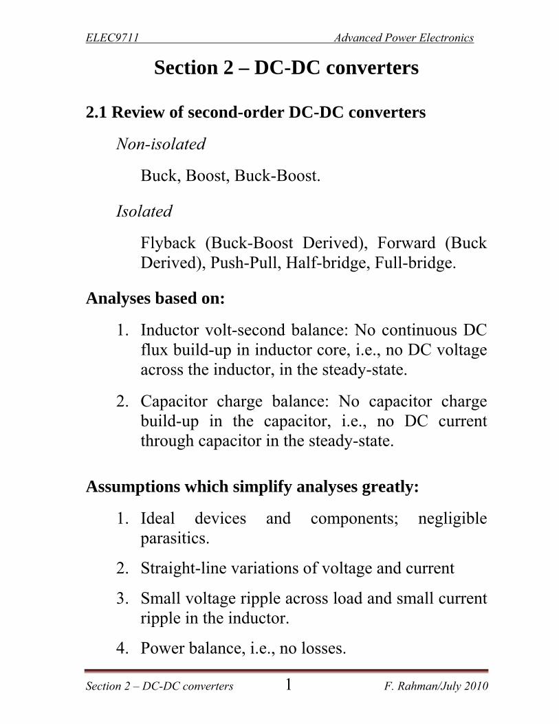
Section 2 – DC-DC converters
2.1 Review of second-order DC-DC converters
Non-isolated
Buck, Boost, Buck-Boost.
Isolated
Flyback (Buck-Boost Derived), Forward (Buck Derived), Push-Pull, Half-bridge, Full-bridge.
Analyses based on:
1. Inductor volt-second balance: No continuous DC flux build-up in inductor core, i.e., no DC voltage across the inductor, in the steady-state.
2. Capacitor charge balance: No capacitor charge build-up in the capacitor, i.e., no DC current through capacitor in the steady-state.
Assumptions which simplify analyses greatly:
1. Ideal devices and components; negligible parasitics.
2. Straight-line variations of voltage and current
3. Small voltage ripple across load and small current ripple in the inductor.
4. Power balance, i.e., no losses.
ELEC9711 Advanced Power Electronics
Section 2 – DC-DC converters 2 F. Rahman/July 2010
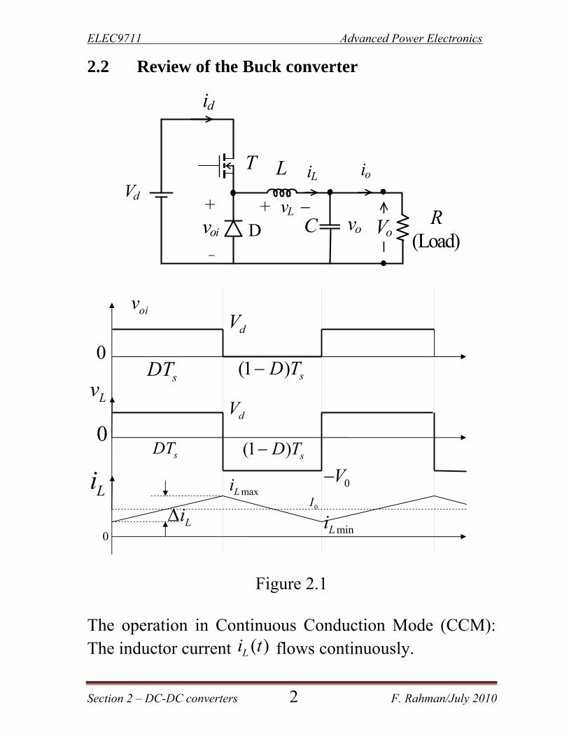
2.2 Review of the Buck converter
+ vL Vd
R (Load)
io
VoC
iLL
D
id
+ voi
vo
T
Figure 2.1
The operation in Continuous Conduction Mode (CCM): The inductor current ( )Li t flows continuously.
dV
0
0dV
0VLi
Lv
0Li
maxLi
minLi
oiv
(1 ) sD TsDT
sDT (1 ) sD T
0I
ELEC9711 Advanced Power Electronics
Section 2 – DC-DC converters 3 F. Rahman/July 2010
When T is ON: The switch conducts the inductor current
Li and the diode (D) reverse biased; 0L dv V V
And L
L
div L
dt
0L ddi V V
dt L
0dL s
V Vi DT
L
When T is OFF: Because of the inductive energy storage,
Li continues to flows through D; 0Lv V
And 0 (1 )L s
Vi D T
L
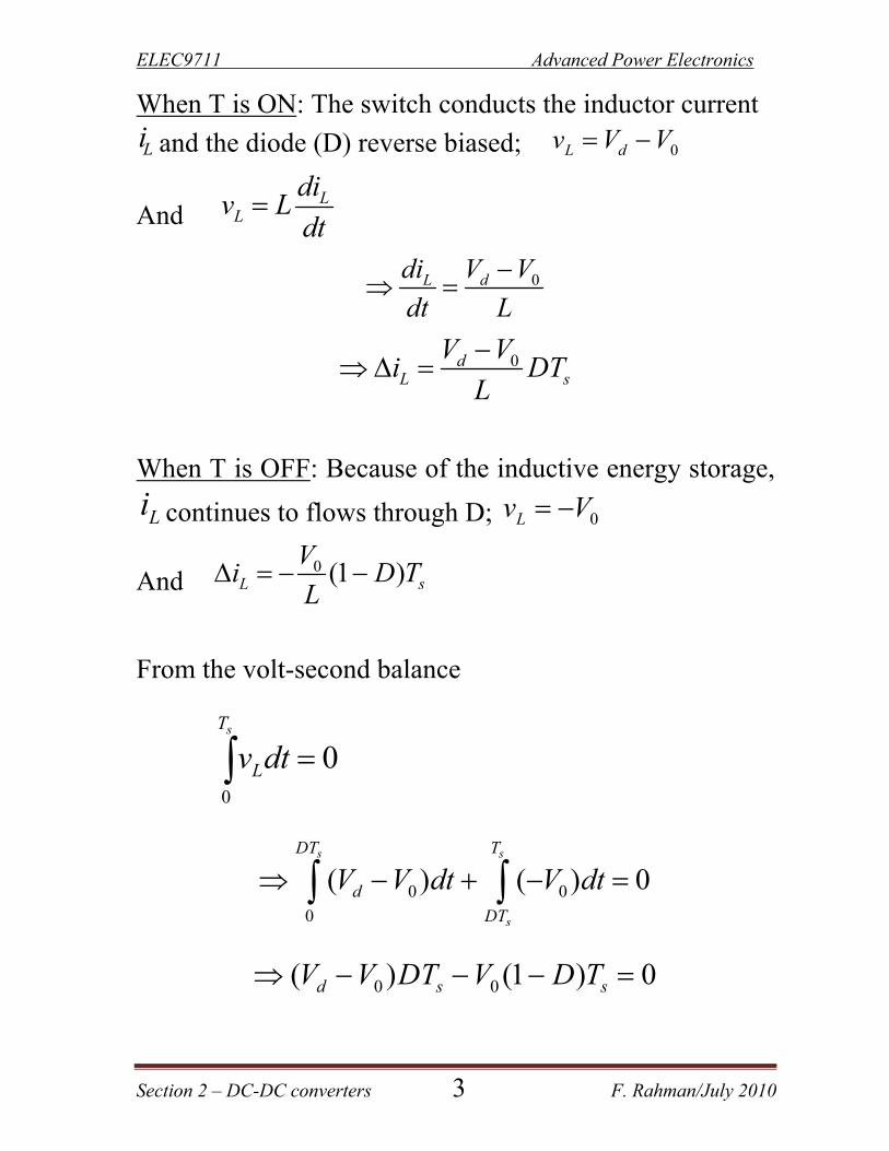
From the volt-second balance
0
0sT
Lv dt
0 0
0
( ) ( ) 0s s
s
DT T
d
DT
V V dt V dt
0 0( ) (1 ) 0d s sV V DT V D T
ELEC9711 Advanced Power Electronics
Section 2 – DC-DC converters 4 F. Rahman/July 2010
0 0d s sV DT V T o
d
VD
V (2.1)
From power balance, 1o
d
I
I D (2.2)
2.2.1 The buck converter in CCM
During 0 ≤ t ≤ DTs, assuming Vd and Vo to be constant,
LL
div L
dt → d oL V Vdi
dt L
During DTs ≤ t ≤ Ts,
L odi V
dt L
From (1) d oL s
V Vi DT
L
(2.3)
1. If (a small) Li is specified, (3) can be used to find the
required value for L, assuming that Ts has already been selected from other considerations.
2. If operation with CCM is desired down to a minimum load, IoB, or ILB, L can be found by setting iomin = 0 for the minimum Io or IL. Note that IL = Io for the Buck converter. This leads to
ELEC9711 Advanced Power Electronics
Section 2 – DC-DC converters 5 F. Rahman/July 2010
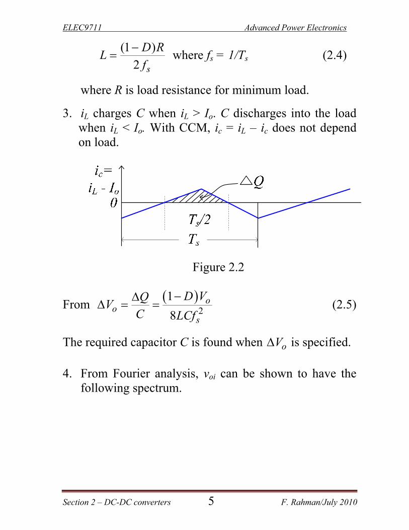
(1 )
2 s
D RL
f
where fs = 1/Ts (2.4)
where R is load resistance for minimum load.
3. iL charges C when iL > Io. C discharges into the load when iL < Io. With CCM, ic = iL – ic does not depend on load.
Figure 2.2
From
2
1
8o
os
D VQV
C LCf
(2.5)
The required capacitor C is found when oV is specified. 4. From Fourier analysis, voi can be shown to have the
following spectrum.
ELEC9711 Advanced Power Electronics
Section 2 – DC-DC converters 6 F. Rahman/July 2010
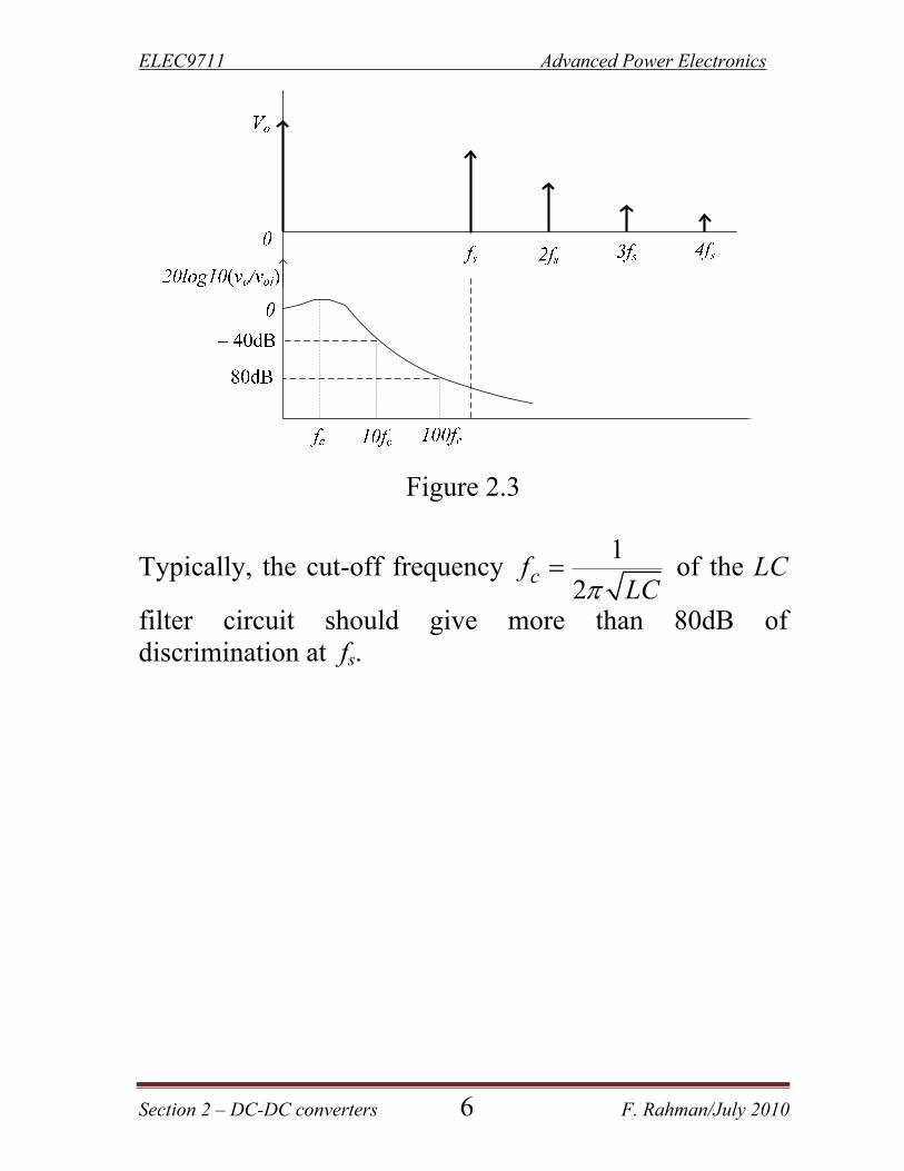
Figure 2.3
Typically, the cut-off frequency 1
2cf
LC of the LC
filter circuit should give more than 80dB of discrimination at fs.
ELEC9711 Advanced Power Electronics
Section 2 – DC-DC converters 7 F. Rahman/July 2010
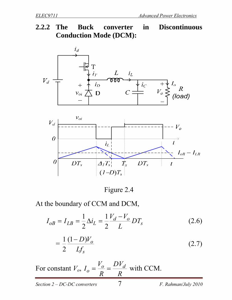
2.2.2 The Buck converter in Discontinuous Conduction Mode (DCM):
Figure 2.4
At the boundary of CCM and DCM,
1 1
2 2d o
oB LB L sV V
I I i DTL
(2.6)
= (1 )1
2o
s
D V
Lf
(2.7)
For constant Vo, o do
V DVI
R R with CCM.
ELEC9711 Advanced Power Electronics
Section 2 – DC-DC converters 8 F. Rahman/July 2010
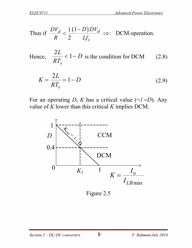
Thus if 11
2dd
s
D DVDV
R Lf
: DCM operation.
Hence, 2
1s
LD
RT is the condition for DCM (2.8)
2
1s
LK D
RT (2.9)
For an operating D, K has a critical value (=1 D). Any value of K lower than this critical K implies DCM.
D
1
0 1
max
o
LB
IK
I
Kcrit = 1 - D
DCM
CCM
0.4
Figure 2.5
ELEC9711 Advanced Power Electronics
Section 2 – DC-DC converters 9 F. Rahman/July 2010
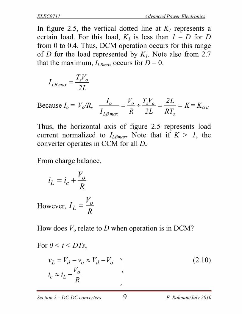
In figure 2.5, the vertical dotted line at K1 represents a certain load. For this load, K1 is less than 1 – D for D from 0 to 0.4. Thus, DCM operation occurs for this range of D for the load represented by K1. Note also from 2.7 that the maximum, ILBmax occurs for D = 0.
s oLB max
T VI
2L
Because Io = Vo/R, o o s o
LB max s
I V T V 2LK
I R 2L RT = Kcrit
Thus, the horizontal axis of figure 2.5 represents load current normalized to ILBmax. Note that if K > 1, the converter operates in CCM for all D. From charge balance,
oL c
Vi i
R
However, oL
VI
R
How does Vo relate to D when operation is in DCM? For 0 < t < DTs,
L d o d ov V v V V (2.10)
oc L
Vi i
R
ELEC9711 Advanced Power Electronics
Section 2 – DC-DC converters 10 F. Rahman/July 2010
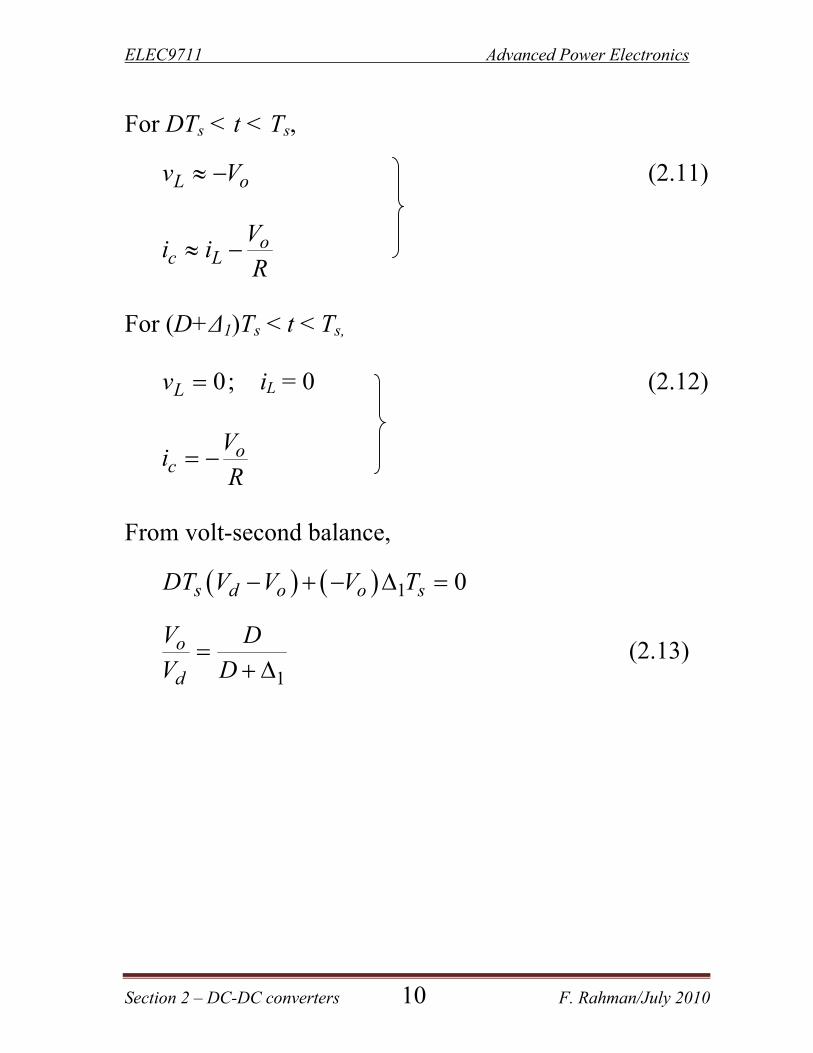
For DTs < t < Ts,
L ov V (2.11)
oc L
Vi i
R
For (D+Δ1)Ts < t < Ts,
0Lv ; iL = 0 (2.12)
oc
Vi
R
From volt-second balance,
1 0s d o o sDT V V V T
1
o
d
V D
V D
(2.13)
ELEC9711 Advanced Power Electronics
Section 2 – DC-DC converters 11 F. Rahman/July 2010
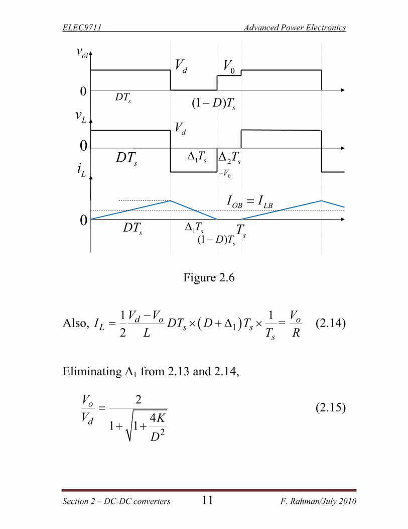
Figure 2.6
Also, 11 1
2d o
L s ss
V VI DT D T
L T
= oV
R (2.14)
Eliminating Δ1 from 2.13 and 2.14,
2
2
41 1
o
d
V
V K
D
(2.15)
dV
0
0dV
0VLi
Lv
0
(1 ) sD TsDT
1 sT2 sT
sDT
OB LBI I
1 sTsDT
sT(1 ) sD T
0Voiv
ELEC9711 Advanced Power Electronics
Section 2 – DC-DC converters 12 F. Rahman/July 2010
o
d
V
V
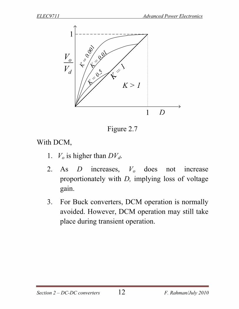
Figure 2.7
With DCM,
1. Vo is higher than DVd.
2. As D increases, Vo does not increase proportionately with D, implying loss of voltage gain.
3. For Buck converters, DCM operation is normally avoided. However, DCM operation may still take place during transient operation.
ELEC9711 Advanced Power Electronics
Section 2 – DC-DC converters 13 F. Rahman/July 2010
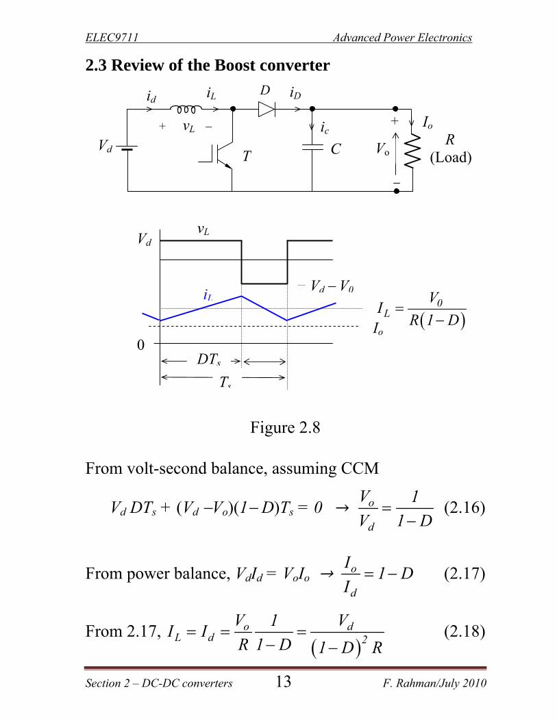
2.3 Review of the Boost converter
Figure 2.8
From volt-second balance, assuming CCM
Vd DTs + (Vd Vo)(1 D)Ts = 0 o
d
V 1
V 1 D
(2.16)
From power balance, VdId = VoIo o
d
I1 D
I (2.17)
From 2.17,
o dL d 2
V V1I I
R 1 D 1 D R
(2.18)
R (Load)
+
iD
+ vL
iL
Vo CVd
ic
D
Io
id
T
Vd
Vd V0iL
0
LV
IR 1 D
0
Ts
DTs
vL
Io
ELEC9711 Advanced Power Electronics
Section 2 – DC-DC converters 14 F. Rahman/July 2010
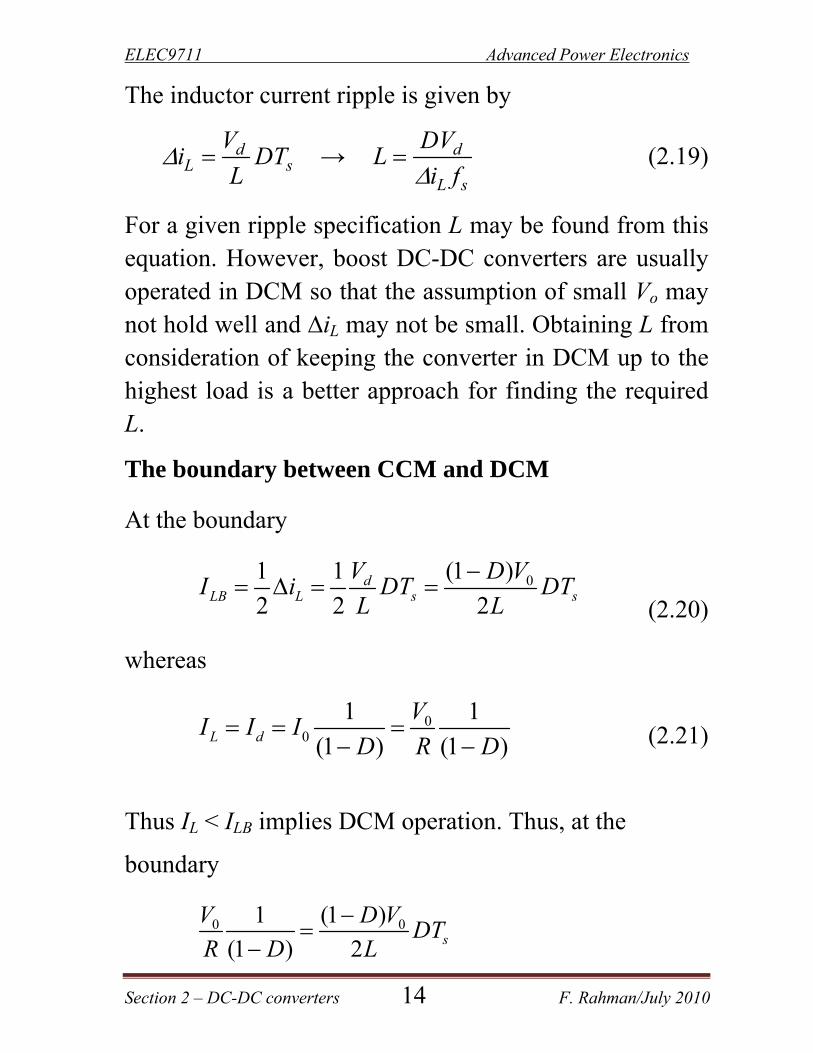
The inductor current ripple is given by
dL s
Vi DT
L → d
L s
DVL
i f (2.19)
For a given ripple specification L may be found from this equation. However, boost DC-DC converters are usually operated in DCM so that the assumption of small Vo may not hold well and ∆iL may not be small. Obtaining L from consideration of keeping the converter in DCM up to the highest load is a better approach for finding the required L.
The boundary between CCM and DCM
At the boundary
01 1 (1 )
2 2 2d
LB L s s
V D VI i DT DT
L L
(2.20)
whereas
00
1 1
(1 ) (1 )L d
VI I I
D R D
(2.21)
Thus IL < ILB implies DCM operation. Thus, at the
boundary
0 01 (1 )
(1 ) 2 s
V D VDT
R D L
ELEC9711 Advanced Power Electronics
Section 2 – DC-DC converters 15 F. Rahman/July 2010
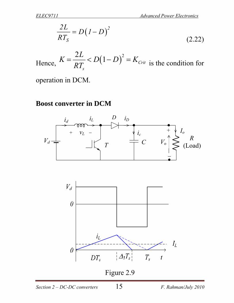
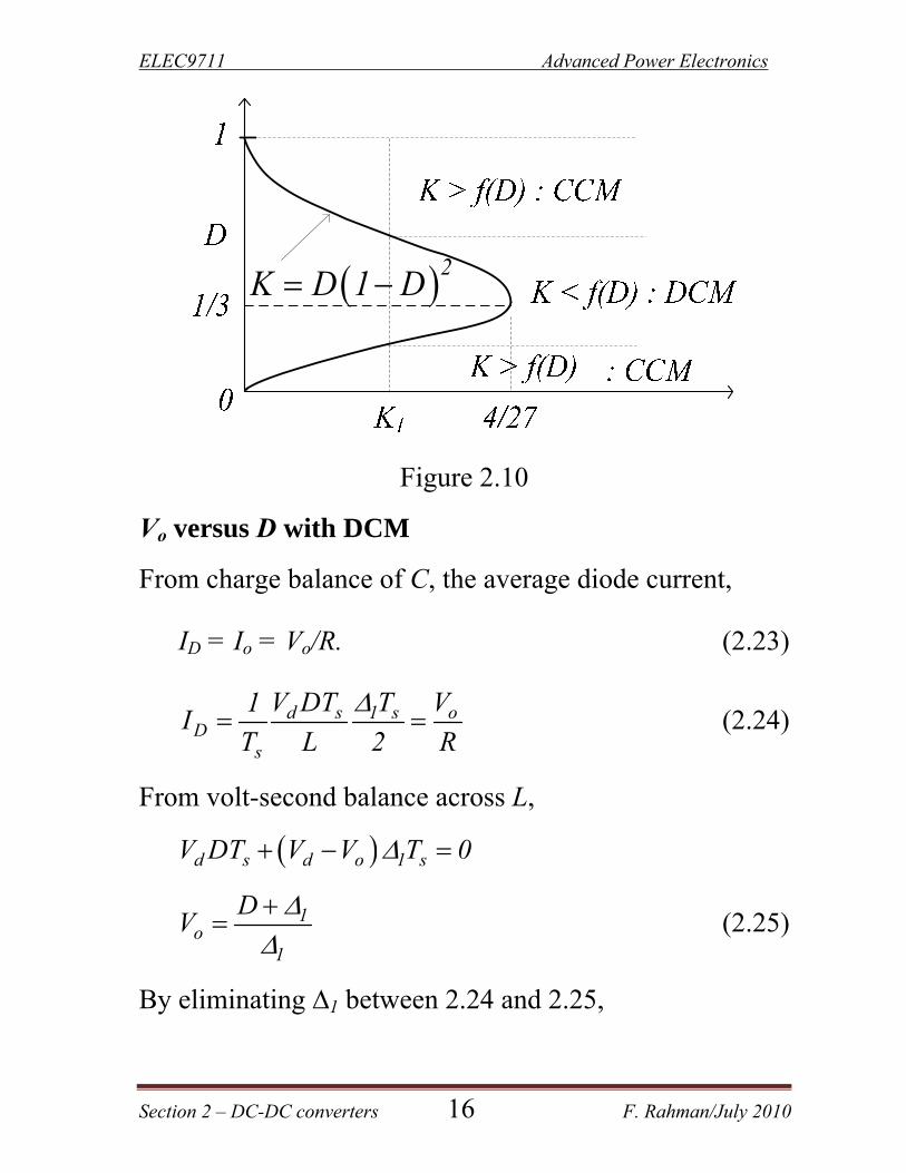
2
S
2LD 1 D
RT
(2.22)
Hence, 221 Crit
s
LK D D K
RT is the condition for
operation in DCM.
Boost converter in DCM
Figure 2.9
R (Load)
+
iD
+ vL
iL
Vo CVd
ic
D
Io
id
T
ELEC9711 Advanced Power Electronics
Section 2 – DC-DC converters 16 F. Rahman/July 2010
2K D 1 D
Figure 2.10
Vo versus D with DCM
From charge balance of C, the average diode current,
ID = Io = Vo/R. (2.23)
d s 1 s oD
s
V DT T V1I
T L 2 R
(2.24)
From volt-second balance across L,
d s d o 1 sV DT V V T 0
1o
1
DV
(2.25)
By eliminating ∆1 between 2.24 and 2.25,
ELEC9711 Advanced Power Electronics
Section 2 – DC-DC converters 17 F. Rahman/July 2010
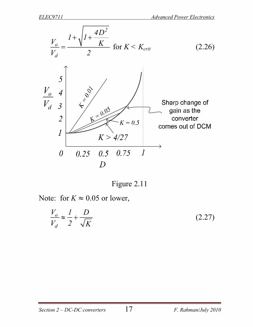
2
o
d
4D1 1
V KV 2
for K < Kcrit (2.26)
o
d
V
V
Figure 2.11
Note: for K 0.05 or lower,
o
d
V 1 D
V 2 K (2.27)
ELEC9711 Advanced Power Electronics
Section 2 – DC-DC converters 18 F. Rahman/July 2010
The Boost (filter) capacitor C and output voltage ripple ∆Vo.
The capacitor C can be found from the consideration that during DTs, C drives the load current Io = Vo/R, which produces the voltage ripple ∆Vo. Thus, charge lost by C during DTs is IoDTs, so that
o so
V DTV
RC (2.28)
C can be specified from this equation. (Note that 2.28 assumes CCM operation).
ELEC9711 Advanced Power Electronics
Section 2 – DC-DC converters 19 F. Rahman/July 2010
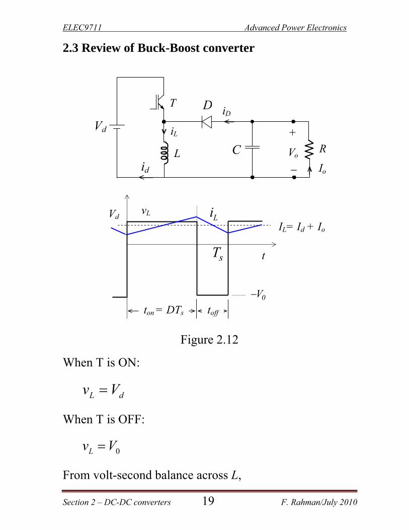
2.3 Review of Buck-Boost converter
D
C R L
T
Vd iL +
Vo
Io id
iD
Figure 2.12
When T is ON:
L dv V
When T is OFF:
0Lv V
From volt-second balance across L,
Vd Li
0V
sT
ton = DTs toff
t
vL
IL= Id + Io
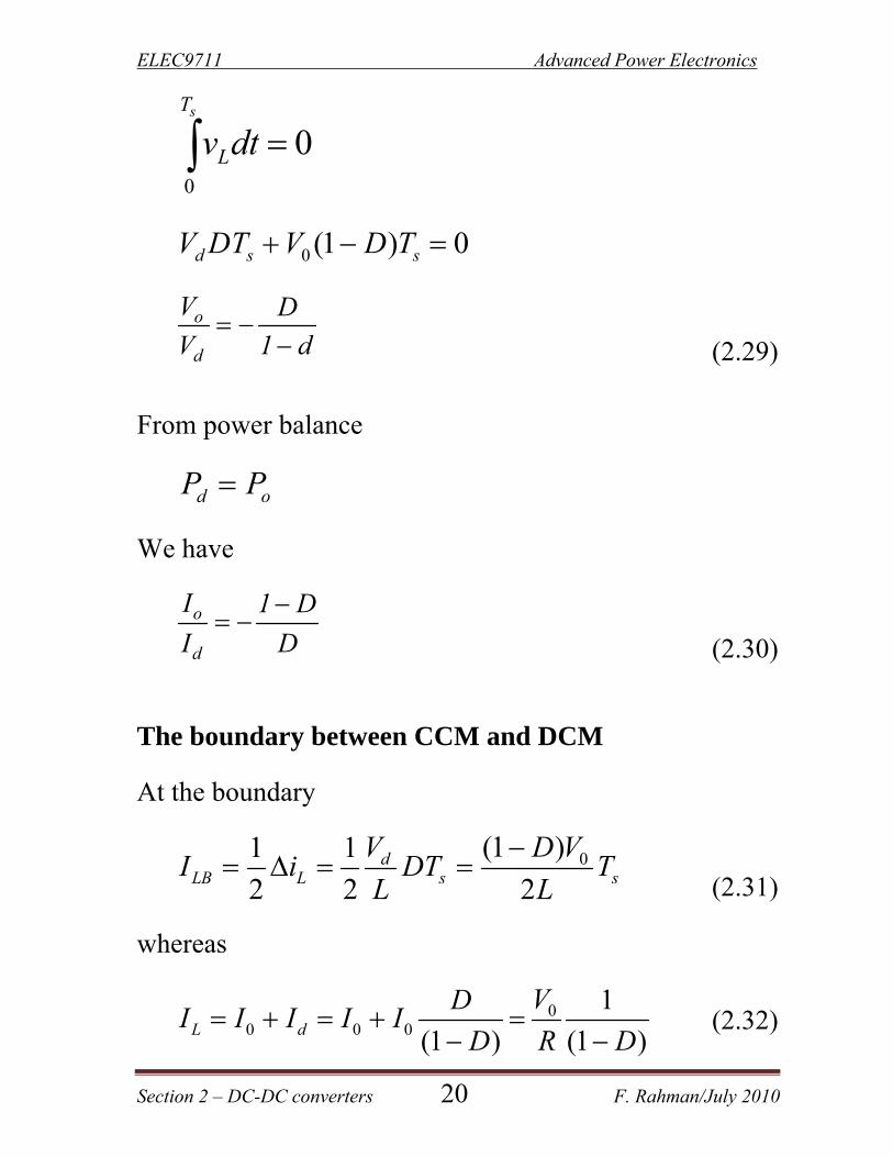
ELEC9711 Advanced Power Electronics
Section 2 – DC-DC converters 20 F. Rahman/July 2010
0
0sT
Lv dt
0 (1 ) 0d s sV DT V D T
o
d
V D
V 1 d
(2.29)
From power balance
d oP P
We have
o
d
I 1 D
I D
(2.30)
The boundary between CCM and DCM
At the boundary
0(1 )1 1
2 2 2d
LB L s s
V D VI i DT T
L L
(2.31)
whereas
0
0 0 0
1
(1 ) (1 )L d
VDI I I I I
D R D
(2.32)
ELEC9711 Advanced Power Electronics
Section 2 – DC-DC converters 21 F. Rahman/July 2010
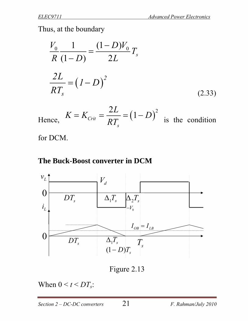
Thus, at the boundary
0 0(1 )1
(1 ) 2 s
V D VT
R D L
2
s
2L1 D
RT
(2.33)
Hence, 221Crit
s
LK K D
RT
is the condition
for DCM.
The Buck-Boost converter in DCM
Figure 2.13
When 0 < t < DTs:
0dV
0VLi
Lv
0
1 sT 2 sTsDT
OB LBI I
1 sTsDT
sT(1 ) sD T
ELEC9711 Advanced Power Electronics
Section 2 – DC-DC converters 22 F. Rahman/July 2010
L dv V
When DTs < t < (D + ∆1)Ts:
0Lv V
When (D + ∆1)Ts < t < Ts:
0Lv
From the volt-second balance across L,
0
0sT
Lv dt
1
1
( )
0
0 ( )
0 0s s s
s s
DT D T T
d
DT D T
V dt V dt dt
0 1( ) 0d s sV DT V T
o
d 1
V D
V
From power balance:
d oP P
ELEC9711 Advanced Power Electronics
Section 2 – DC-DC converters 23 F. Rahman/July 2010
d
o 1
I D
I
So
00
1 1d
D D VI I
R
Moreover, in DCM, we have
o o o1
L d o1 1
V V VDDI I I
R R R
Where
1 1
1 1.( ) . .( )
2 2d d
L s s ss
V VI DT D T DT D
L T L
So 1 0
11
.( )2
ds
V D VDT D
L R
0 01
2 1 1
s d d
L V VK
RT V D V D
From 0
1d
V D
V
0
0 1d
d
V DVV KV D
ELEC9711 Advanced Power Electronics
Section 2 – DC-DC converters 24 F. Rahman/July 2010
2
20
d
VK D
V
o
d
V D
V K (2.34)
Output voltage ripple
o s o s
oI DT V DTQ
VC C RC
(2.35)
ELEC9711 Advanced Power Electronics
Section 2 – DC-DC converters 25 F. Rahman/July 2010
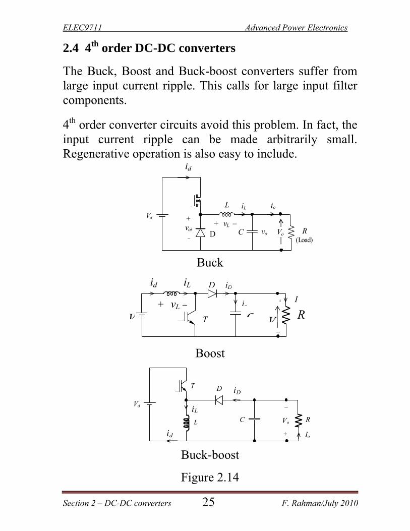
2.4 4th order DC-DC converters
The Buck, Boost and Buck-boost converters suffer from large input current ripple. This calls for large input filter components.
4th order converter circuits avoid this problem. In fact, the input current ripple can be made arbitrarily small. Regenerative operation is also easy to include.
Buck
Boost
Buck-boost
Figure 2.14
Vd
R (Load)
io
VoC
iLL
+ vL D
id
+voi
vo
D
C R L
T
Vd iL
Vo
+ Io id
iD
R +
iD
+ vL
iL
VCVic
D
I
id
T
ELEC9711 Advanced Power Electronics
Section 2 – DC-DC converters 26 F. Rahman/July 2010
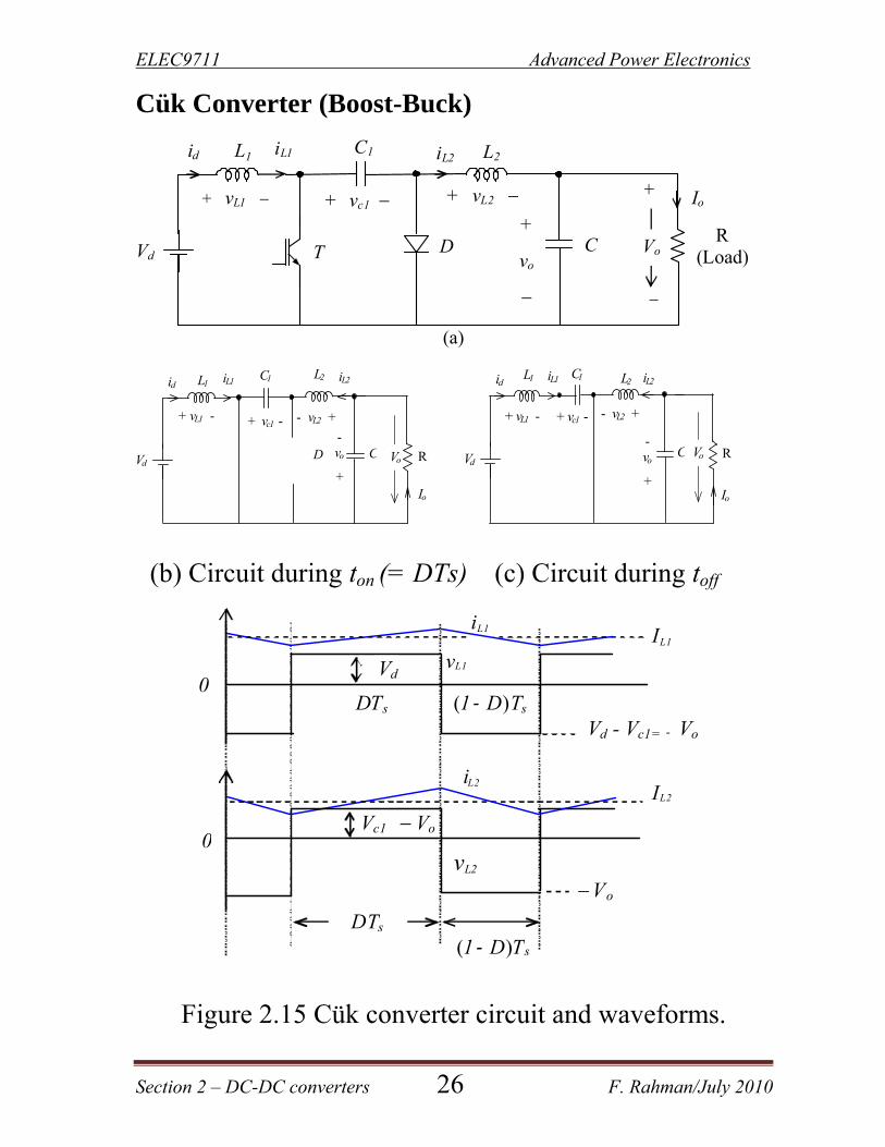
Cük Converter (Boost-Buck) L1 iL1 C1 L2iL2
+ vL1 + vc1 + vL2
+
vo
C R (Load)
Vd Vo
id
+
DT
Io
(a)
L1 iL1 C1 L2 iL2
+ vL1 - + vc1 - - vL2 +
- vo
+
C RVd Vo
id
D
Io
L1 iL1 C1 L2 iL2
+ vL1 - + vc1 - - vL2 +
- vo
+
C RVdVo
id
Io
(b) Circuit during ton (= DTs) (c) Circuit during toff
DTs
(1‐ D)Ts
iL1
vL1 Vd
Vd - Vc1= ‐ Vo
vL2
iL2
0
0
IL1
IL2
Vc1 Vo
Vo
DTs (1‐ D)Ts
Figure 2.15 Cük converter circuit and waveforms.
ELEC9711 Advanced Power Electronics
Section 2 – DC-DC converters 27 F. Rahman/July 2010
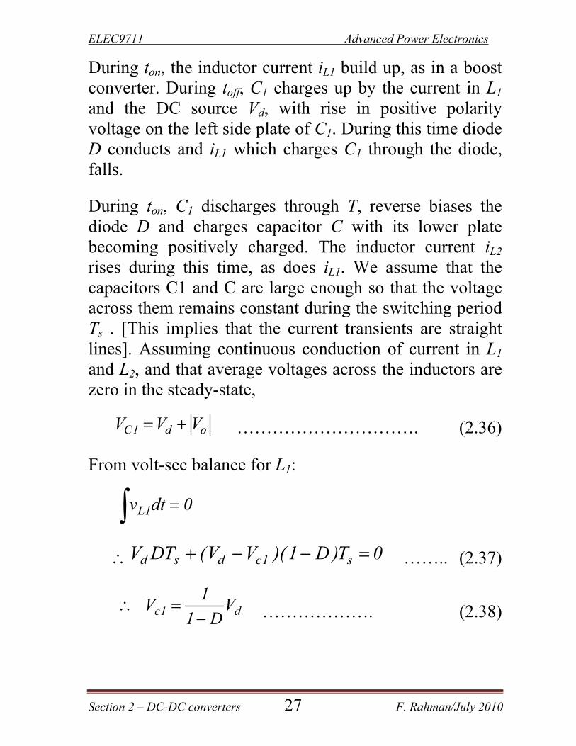
During ton, the inductor current iL1 build up, as in a boost converter. During toff, C1 charges up by the current in L1 and the DC source Vd, with rise in positive polarity voltage on the left side plate of C1. During this time diode D conducts and iL1 which charges C1 through the diode, falls.
During ton, C1 discharges through T, reverse biases the diode D and charges capacitor C with its lower plate becoming positively charged. The inductor current iL2 rises during this time, as does iL1. We assume that the capacitors C1 and C are large enough so that the voltage across them remains constant during the switching period Ts . [This implies that the current transients are straight lines]. Assuming continuous conduction of current in L1 and L2, and that average voltages across the inductors are zero in the steady-state,
C1 d oV V V …………………………. (2.36)
From volt-sec balance for L1:
L1v dt 0
d s d c1 sV DT (V V )(1 D )T 0 …….. (2.37)
c1 d1
V V1 D
………………. (2.38)
ELEC9711 Advanced Power Electronics
Section 2 – DC-DC converters 28 F. Rahman/July 2010
From volt-second balance for L2:
L2v dt 0
c1 0 0 s(V V )DTs ( V )(1 D )T 0 …… (2.39)
c1 o1
V VD
……………………… (2.40)
o
d
V D
V 1 D
……………………… (2.41)
From power balance,
D
D
I
I
d
10 …………………. (2.42)
d d
L1 s1 1 s
V V Di DT
L L f ………….. (2.43)
c1 o d
L2 s2 2 s
V V V Di DT
L L f
…………….. (2.44)
From 2.43 and 2.44, it is clear that ∆iL1 and ∆iL2 both be made arbitrarily small by selecting fs, L1 and L2 appropriately.
Note that for this converter,
IL1 = Id , Io = IL2 , where o
oV
IR
. (2.45)
ELEC9711 Advanced Power Electronics
Section 2 – DC-DC converters 29 F. Rahman/July 2010
Also from power balance,
d L1 o L2V I V I so that oL1
L2 d
VI
I V (2.46)
From (2.41) and (2.42),
2
dL1 2
D VI
R( 1 D )
……………………. (2.47)
As before,
2
L1 d dL1,min L1 2
1 s
i D V DVi I
2 2L fR( 1 D )
For continuous conduction, L1,mini 0 ,
2
1mins
( 1 D ) RL
2Df
so that
2
s
1 D2L
RT D
(2.48)
Similarly, for continuous conduction
2mins
( 1 D )RL
2 f
so that 2
s
2L1 D
RT (2.49)
Note that the output stage comprising of L2, C, R and D is similar to the buck converter, so that by analogy, the output filter capacitor value is given by,
o
2o 2 s
V 1 D
V 8L Cf
(2.50)
ELEC9711 Advanced Power Electronics
Section 2 – DC-DC converters 30 F. Rahman/July 2010
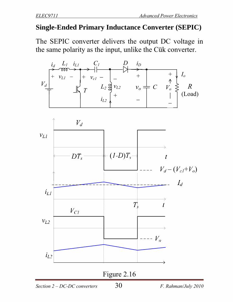
Single-Ended Primary Inductance Converter (SEPIC)
The SEPIC converter delivers the output DC voltage in the same polarity as the input, unlike the Cük converter.
L1 iL1 C1 D
iL2
+ vL1 + vc1 vL2
+
+
vo
C R (Load)
Vd Vo
id
+
L2T
Io
iD
Figure 2.16
ELEC9711 Advanced Power Electronics
Section 2 – DC-DC converters 31 F. Rahman/July 2010
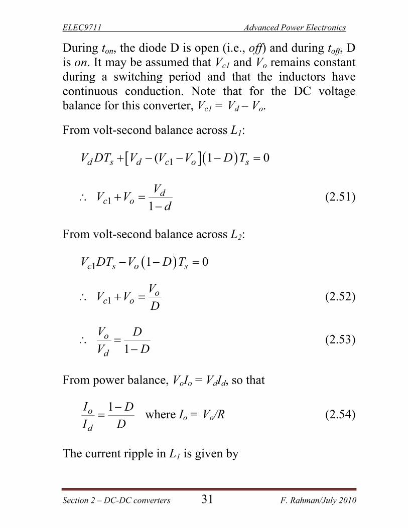
During ton, the diode D is open (i.e., off) and during toff, D is on. It may be assumed that Vc1 and Vo remains constant during a switching period and that the inductors have continuous conduction. Note that for the DC voltage balance for this converter, Vc1 = Vd – Vo.
From volt-second balance across L1: 1( 1 0d s d c o sV DT V V V D T
1 1d
c oV
V Vd
(2.51)
From volt-second balance across L2: 1 1 0c s o sV DT V D T
1o
c oV
V VD
(2.52)
1
o
d
V DV D
(2.53)
From power balance, VoIo = VdId, so that
1o
d
I DI D
where Io = Vo/R (2.54)
The current ripple in L1 is given by
ELEC9711 Advanced Power Electronics
Section 2 – DC-DC converters 32 F. Rahman/July 2010
11 1 1
1 1o od s sL
s
V D D VV DT DTi
L D L L f
(2.55)
The current ripple in L1 is given by
1
22 2
1 ocL s
s
D VVi DT
L L f
(2.56)
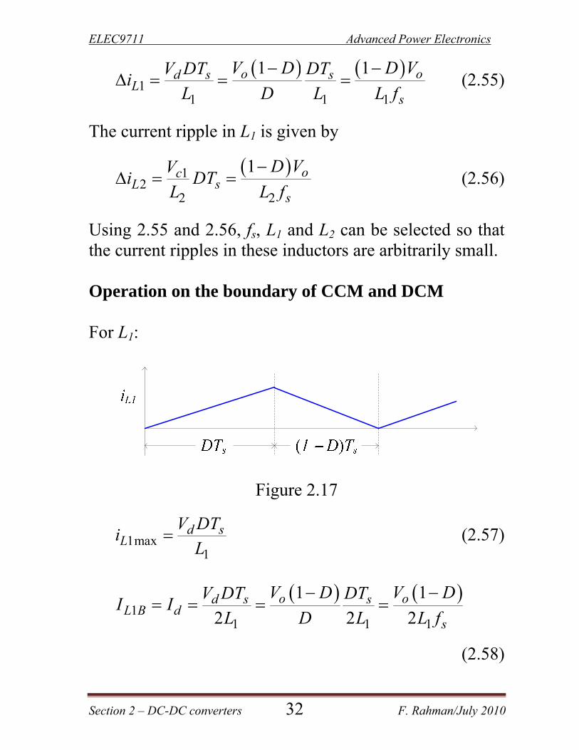
Using 2.55 and 2.56, fs, L1 and L2 can be selected so that the current ripples in these inductors are arbitrarily small. Operation on the boundary of CCM and DCM For L1:
Figure 2.17
1max1
d sL
V DTi
L (2.57)
11 1 1
1 1
2 2 2o od s s
L B ds
V D V DV DT DTI I
L D L L f
(2.58)
ELEC9711 Advanced Power Electronics
Section 2 – DC-DC converters 33 F. Rahman/July 2010
For Io = Vo/R, 1
od
V DI
R D
(2.59)
Now, Id > IL1B implies CCM, and Id < IL1B implies DCM. The boundary between CCM and DCM in L1 is given by
1
1
1 2oo
s
V DV DR D L f
.
21 12
s
DLK
RT D
for operation in CCM (2.60)
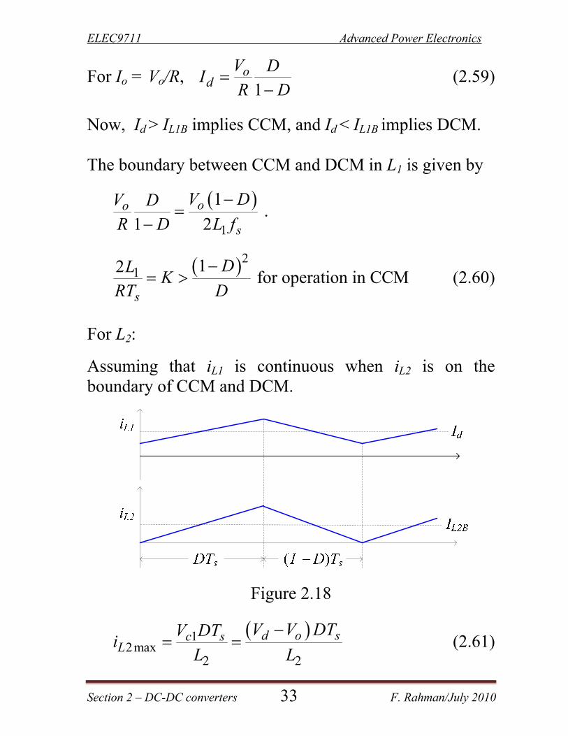
For L2:
Assuming that iL1 is continuous when iL2 is on the boundary of CCM and DCM.
Figure 2.18
1
2max2 2
d o sc sL
V V DTV DTi
L L
(2.61)
ELEC9711 Advanced Power Electronics
Section 2 – DC-DC converters 34 F. Rahman/July 2010
222
d o sL B
V V DTI
L
(2.62)
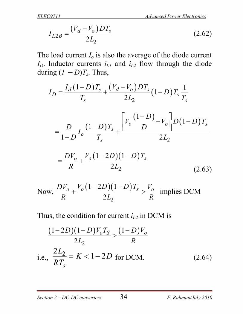
The load current Io is also the average of the diode current ID. Inductor currents iL1 and iL2 flow through the diode during (1 D)Ts. Thus,
2
1 11
2d o sd s
D ss s
V V DTI D TI D T
T L T
2
11
1
1 2
o o ss
os
DV V D D T
D TD DI
D T L
2
1 2 1
2o so V D D TDV
R L
(2.63)
Now,
2
1 2 1
2o so oV D D TDV V
R L R
implies DCM
Thus, the condition for current iL2 in DCM is
2
1 2 1 1
2o S oD D V T D V
L R
i.e., 221 2
s
LK D
RT for DCM. (2.64)