Embed Size (px)
Citation preview
Electrical Circuits
Department of Biomedical Engineering
University of Warith Al-Anbiyaa
1
2.15 KIRCHHOFF’S LAWS
Ohm’s law by itself is not sufficient to analyze circuits. However, when it is coupled
with Kirchhoff’s two laws, we have a sufficient, powerful set of tools for analyzing a large
variety of electric circuits. Kirchhoff’s laws were first introduced in 1847 by the German
physicist Gustav Robert Kirchhoff (1824–1887). These laws are formally known as
Kirchhoff’s current law (KCL) and Kirchhoff’s voltage law (KVL).
2.15.1 Kirchhoff’s current law
Kirchhoff’s first law is based on the law of conservation of charge, which requires
that the algebraic sum of charges within a system cannot change.
Kirchhoff’s current law (KCL) states that the algebraic sum of currents entering a
node (or a closed boundary) is zero.
Mathematically, KCL implies that
∑ 𝒊𝒏𝑵𝒏=𝟏 = 0 (2.38)
where N is the number of branches connected to the node and in is the nth current entering
(or leaving) the node. By this law, currents entering a node may be regarded as positive,
while currents leaving the node may be taken as negative or vice versa. To prove KCL,
assume a set of currents ik(t ), k = 1, 2, . . . , flow into a node. The algebraic sum of currents
at the node is
iT (t) = i1(t) + i2(t) + i3(t)+· · · (2.39)
Integrating both sides of Eq. (2.39) gives
qT (t) = q1(t) + q2(t) + q3(t)+· · · (2.40)
where qk(t) = ∫ ik(t) dt and qT(t) = ∫ iT(t) dt . But the law of conservation of electric
charge requires that the algebraic sum of electric charges at the node must not change; that
is, the node stores no net charge. Thus qT (t) = 0 → iT (t) = 0, confirming the validity of
KCL.
Electrical Circuits
Department of Biomedical Engineering
University of Warith Al-Anbiyaa
2
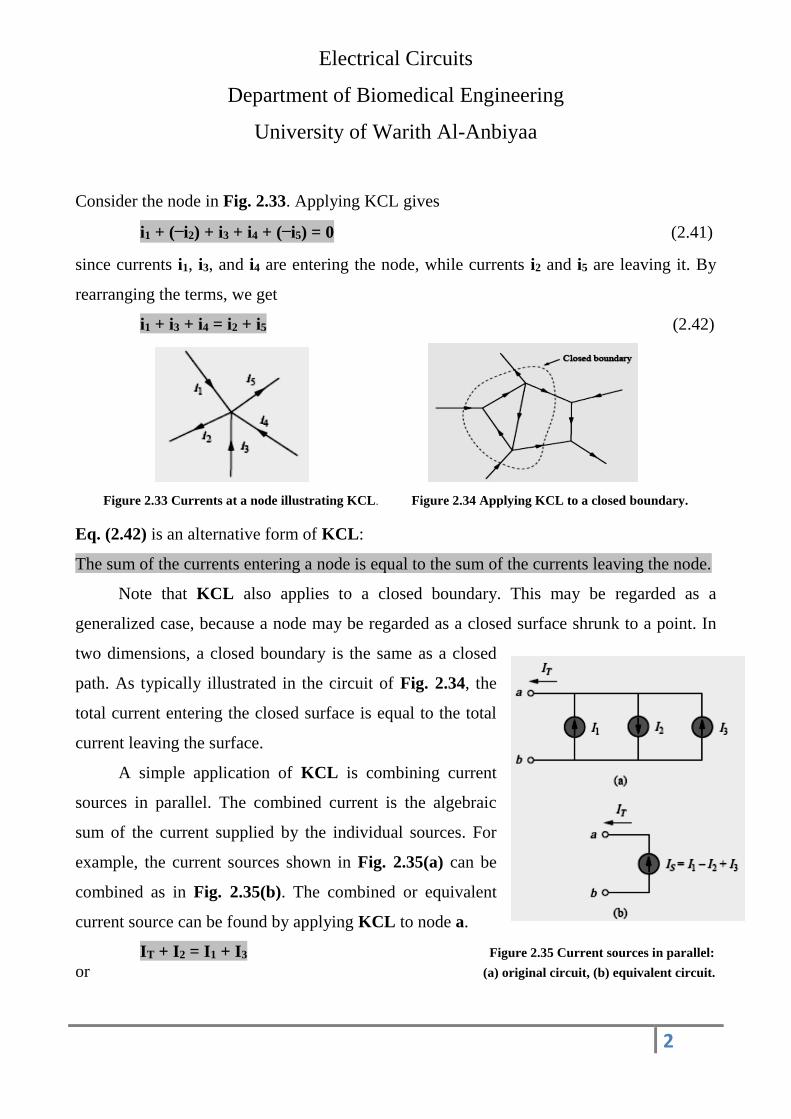
Consider the node in Fig. 2.33. Applying KCL gives
i1 + (−i2) + i3 + i4 + (−i5) = 0 (2.41)
since currents i1, i3, and i4 are entering the node, while currents i2 and i5 are leaving it. By
rearranging the terms, we get
i1 + i3 + i4 = i2 + i5 (2.42)
Figure 2.33 Currents at a node illustrating KCL. Figure 2.34 Applying KCL to a closed boundary.
Eq. (2.42) is an alternative form of KCL:
The sum of the currents entering a node is equal to the sum of the currents leaving the node.
Note that KCL also applies to a closed boundary. This may be regarded as a
generalized case, because a node may be regarded as a closed surface shrunk to a point. In
two dimensions, a closed boundary is the same as a closed
path. As typically illustrated in the circuit of Fig. 2.34, the
total current entering the closed surface is equal to the total
current leaving the surface.
A simple application of KCL is combining current
sources in parallel. The combined current is the algebraic
sum of the current supplied by the individual sources. For
example, the current sources shown in Fig. 2.35(a) can be
combined as in Fig. 2.35(b). The combined or equivalent
current source can be found by applying KCL to node a.
IT + I2 = I1 + I3 Figure 2.35 Current sources in parallel:
or (a) original circuit, (b) equivalent circuit.
Electrical Circuits
Department of Biomedical Engineering
University of Warith Al-Anbiyaa
3
IT = I1 − I2 + I3 (2.43)
A circuit cannot contain two different currents, I1 and I2, in series, unless I1 = I2; otherwise
KCL will be violated.
2.15.2 Kirchhoff’s voltage law
Kirchhoff’s second law is based on the principle of conservation of energy:
Kirchhoff’s voltage law (KVL) states that the algebraic sum of all voltages around a closed
path (or loop) is zero.
Expressed mathematically, KVL states that
∑ 𝒗𝒎𝑴𝒎=𝟏 = 0 (2.44)
Where M is the number of voltages in the loop (or the number of branches in the loop) and
vm is the mth voltage.
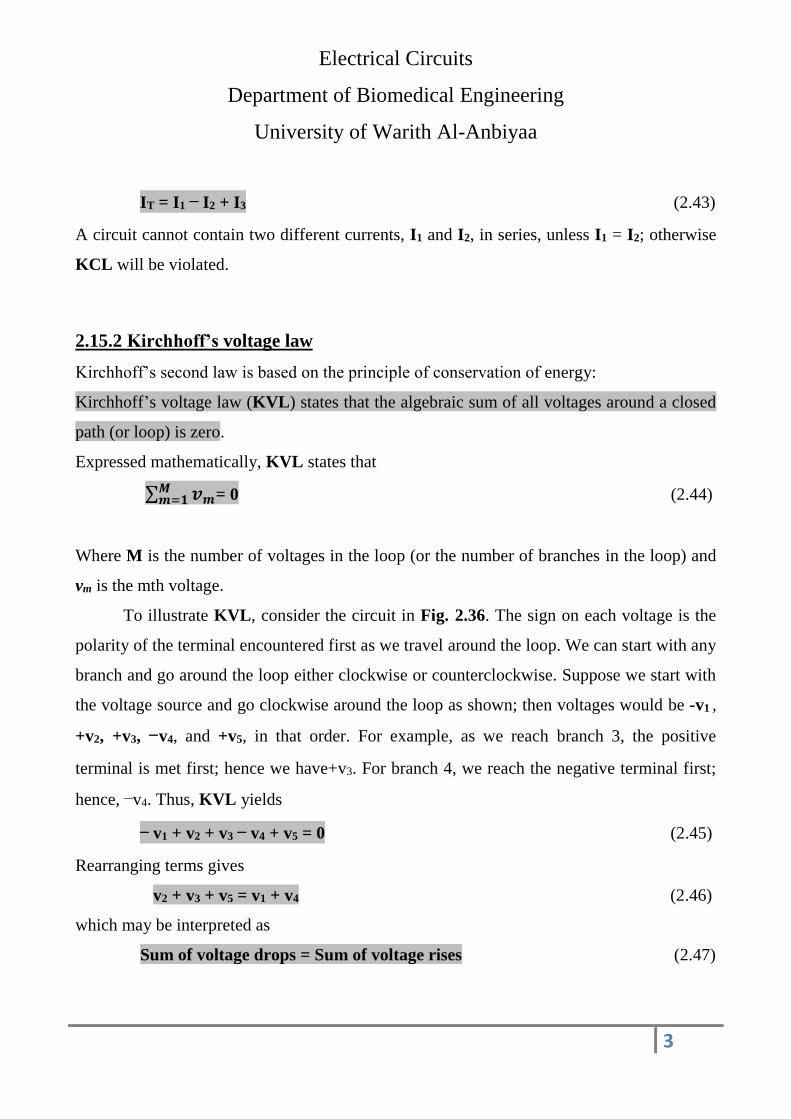
To illustrate KVL, consider the circuit in Fig. 2.36. The sign on each voltage is the
polarity of the terminal encountered first as we travel around the loop. We can start with any
branch and go around the loop either clockwise or counterclockwise. Suppose we start with
the voltage source and go clockwise around the loop as shown; then voltages would be -v1 ,
+v2, +v3, −v4, and +v5, in that order. For example, as we reach branch 3, the positive
terminal is met first; hence we have+v3. For branch 4, we reach the negative terminal first;
hence, −v4. Thus, KVL yields
− v1 + v2 + v3 − v4 + v5 = 0 (2.45)
Rearranging terms gives
v2 + v3 + v5 = v1 + v4 (2.46)
which may be interpreted as
Sum of voltage drops = Sum of voltage rises (2.47)
Electrical Circuits
Department of Biomedical Engineering
University of Warith Al-Anbiyaa
4
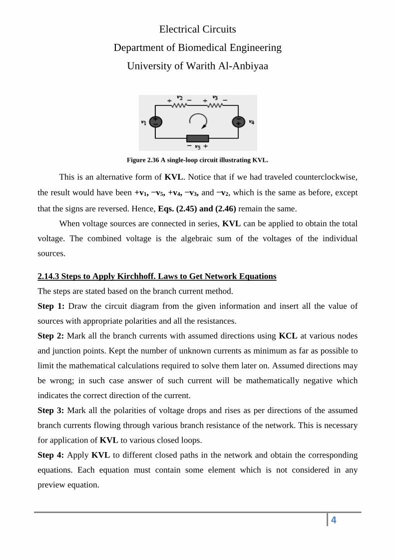
Figure 2.36 A single-loop circuit illustrating KVL.
This is an alternative form of KVL. Notice that if we had traveled counterclockwise,
the result would have been +v1, −v5, +v4, −v3, and −v2, which is the same as before, except
that the signs are reversed. Hence, Eqs. (2.45) and (2.46) remain the same.
When voltage sources are connected in series, KVL can be applied to obtain the total
voltage. The combined voltage is the algebraic sum of the voltages of the individual
sources.
2.14.3 Steps to Apply Kirchhoff. Laws to Get Network Equations
The steps are stated based on the branch current method.
Step 1: Draw the circuit diagram from the given information and insert all the value of
sources with appropriate polarities and all the resistances.
Step 2: Mark all the branch currents with assumed directions using KCL at various nodes
and junction points. Kept the number of unknown currents as minimum as far as possible to
limit the mathematical calculations required to solve them later on. Assumed directions may
be wrong; in such case answer of such current will be mathematically negative which
indicates the correct direction of the current.
Step 3: Mark all the polarities of voltage drops and rises as per directions of the assumed
branch currents flowing through various branch resistance of the network. This is necessary
for application of KVL to various closed loops.
Step 4: Apply KVL to different closed paths in the network and obtain the corresponding
equations. Each equation must contain some element which is not considered in any
preview equation.
Electrical Circuits
Department of Biomedical Engineering
University of Warith Al-Anbiyaa
5
2.16 Solving Simultaneous Equations and Cramer's Rule
Electric circuit analysis with the help of Kirchhoff’s laws usually involves solution of
two or three simultaneous equations. These equations can be solved by a systematic
elimination of the variables but the procedure is often lengthy and laborious and hence more
liable to error. Determinants and Cramer’s rule provide a simple and straight method for
solving network equations through manipulation of their coefficients. Of course, if the
number of simultaneous equations happens to be very large, use of a digital computer can
make the task easy. Let us assume that set of simultaneous equations obtained is, as
follows,
where C1, C2, ………, Cn constants. Then Cramer's rule says that form a system
determinant Δ or D as,
𝜟 = [
𝒂𝟏𝟏 𝒂𝟏𝟐 ⋯ 𝒂𝟏𝒏
𝒂𝟐𝟏 𝒂𝟐𝟐....
⋯ 𝒂𝟐𝒏
𝒂𝒏𝟏 𝒂𝒏𝟐 ⋯ 𝒂𝒏𝒏
] = 𝑫
Then obtain the subdeterminant Dj by replacing jth column of Δ by the column of
constants existing on right hand side of equations i.e. C1, C2, .... Cn;
𝑫𝟏 = [
𝑪𝟏 𝒂𝟏𝟐 ⋯ 𝒂𝟏𝒏
𝑪𝒏 𝒂𝟐𝟐....
⋯ 𝒂𝟐𝒏
𝑪𝒏 𝒂𝒏𝟐 ⋯ 𝒂𝒏𝒏
] , 𝑫𝟐 = [
𝒂𝟏𝟏 𝑪𝟏 ⋯ 𝒂𝟏𝒏
𝒂𝟐𝟏 𝑪𝟐....
⋯ 𝒂𝟐𝒏
𝒂𝒏𝟏 𝑪𝒏 ⋯ 𝒂𝒏𝒏
]
and 𝑫𝒏 = [
𝒂𝟏𝟏 𝒂𝟏𝟐 ⋯ 𝑪𝟏
𝒂𝟐𝟏 𝒂𝟐𝟐....
⋯ 𝑪𝟐
𝒂𝒏𝟏 𝒂𝒏𝟐 ⋯ 𝑪𝒏
]
a11 x1+ a12 x2+………….+ a1n xn= C1
a21 x1+ a22 x2+………….+ a2n xn= C2
.
.
an1 x1+ an2 x2+…………+ ann xn= Cn
Electrical Circuits
Department of Biomedical Engineering
University of Warith Al-Anbiyaa
6
The unknowns of the equations are given by Cramer's rule as,
𝑿𝟏 =𝑫𝟏
𝑫, 𝑿𝟐 =
𝑫𝟐
𝑫, ⋯ , 𝑿𝒏 =
𝑫𝒏
𝑫
Where D1, D2, …, Dn and D are values of the respective determents
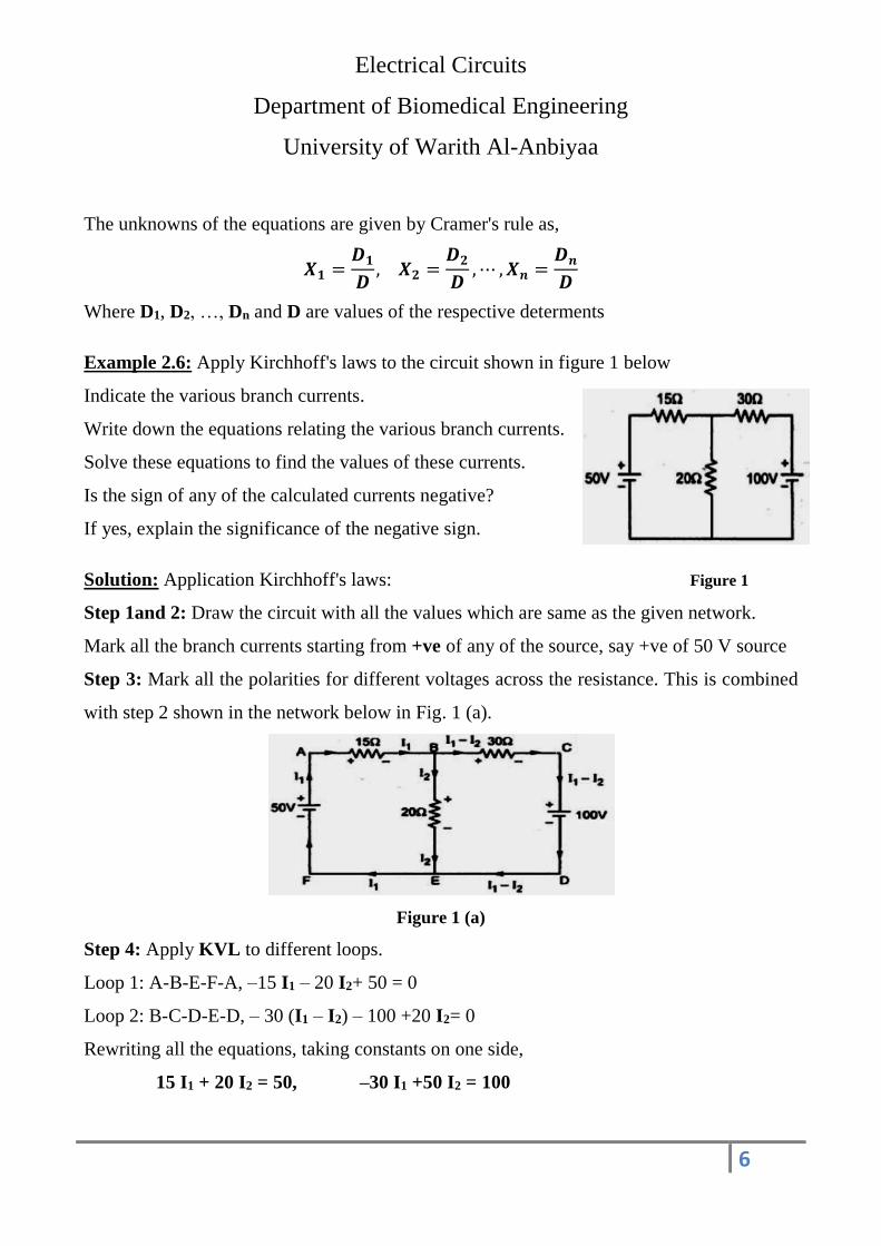
Example 2.6: Apply Kirchhoff's laws to the circuit shown in figure 1 below
Indicate the various branch currents.
Write down the equations relating the various branch currents.
Solve these equations to find the values of these currents.
Is the sign of any of the calculated currents negative?
If yes, explain the significance of the negative sign.
Solution: Application Kirchhoff's laws: Figure 1
Step 1and 2: Draw the circuit with all the values which are same as the given network.
Mark all the branch currents starting from +ve of any of the source, say +ve of 50 V source
Step 3: Mark all the polarities for different voltages across the resistance. This is combined
with step 2 shown in the network below in Fig. 1 (a).
Figure 1 (a)
Step 4: Apply KVL to different loops.
Loop 1: A-B-E-F-A, –15 I1 – 20 I2+ 50 = 0
Loop 2: B-C-D-E-D, – 30 (I1 – I2) – 100 +20 I2= 0
Rewriting all the equations, taking constants on one side,
15 I1 + 20 I2 = 50, –30 I1 +50 I2 = 100
Electrical Circuits
Department of Biomedical Engineering
University of Warith Al-Anbiyaa
7
Apply Cramer's rule, 𝐷 = |15 20
−30 50| = 1350
Calculating D1, 𝐷1 = |50 20
100 50| = 500
𝐼1 =𝐷1
𝐷=
500
1350= 0.37 𝐴
Calculating D2, 𝐷2 = |15 50
−30 100| = 3000
𝐼2 =𝐷2
𝐷=
3000
1350= 2.22 𝐴
For I1 and I2 as answer is positive, assumed direction is correct.
: . For I1 answer is 0.37 A. For I2 answer is 2.22 A
I1 –I2 = 0.37 – 2.22 = – 1.85 A
Negative sign indicates assumed direction is wrong.
i.e. I1 – I2 = 1.85 A flowing in opposite direction to that of the assumed direction.
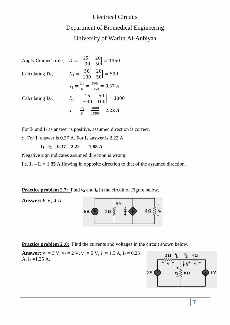
Practice problem 2.7: Find vo and io in the circuit of Figure below.
Answer: 8 V, 4 A.
Practice problem 2 .8: Find the currents and voltages in the circuit shown below.
Answer: v1 = 3 V, v2 = 2 V, v3 = 5 V, i1 = 1.5 A, i2 = 0.25
A, i3 =1.25 A.
Electrical Circuits
Department of Biomedical Engineering
University of Warith Al-Anbiyaa
8
Methods of Analysis
3.1 INTRODUCTION
Having understood the fundamental laws of circuit theory (Ohm’s law and
Kirchhoff’s laws), we are now prepared to apply these laws to develop two powerful
techniques for circuit analysis: nodal analysis, which is based on a systematic application of
Kirchhoff’s current law (KCL), and mesh analysis, which is based on a systematic
application of Kirchhoff’s voltage law (KVL). The two techniques are so important that this
chapter should be regarded as the most important in the lectures.
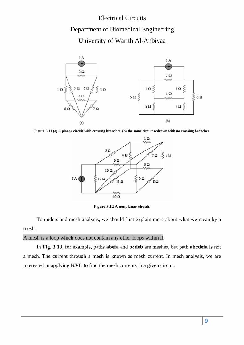
3.3 MESH ANALYSIS
Mesh analysis provides another general procedure for analyzing circuits, using mesh
currents as the circuit variables. Using mesh currents instead of element currents as circuit
variables is convenient and reduces the number of equations that must be solved
simultaneously. Recall that a loop is a closed path with no node passed more than once. A
mesh is a loop that does not contain any other loop within it.
Nodal analysis applies KCL to find unknown voltages in a given circuit, while mesh
analysis applies KVL to find unknown currents. Mesh analysis is not quite as general as
nodal analysis because it is only applicable to a circuit that is planar. A planar circuit is one
that can be drawn in a plane with no branches crossing one another; otherwise it is
nonplanar. A circuit may have crossing branches and still be planar if it can be redrawn
such that it has no crossing branches. For example, the circuit in Fig. 3.11(a) has two
crossing branches, but it can be redrawn as in Fig. 3.11(b). Hence, the circuit in Fig. 3.11(a)
is planar. However, the circuit in Fig. 3.12 is nonplanar, because there is no way to redraw
it and avoid the branches crossing. Nonplanar circuits can be handled using nodal analysis,
but they will not be considered in this text.
Electrical Circuits
Department of Biomedical Engineering
University of Warith Al-Anbiyaa
9
Figure 3.11 (a) A planar circuit with crossing branches, (b) the same circuit redrawn with no crossing branches.
Figure 3.12 A nonplanar circuit.
To understand mesh analysis, we should first explain more about what we mean by a
mesh.
A mesh is a loop which does not contain any other loops within it.
In Fig. 3.13, for example, paths abefa and bcdeb are meshes, but path abcdefa is not
a mesh. The current through a mesh is known as mesh current. In mesh analysis, we are
interested in applying KVL to find the mesh currents in a given circuit.
Electrical Circuits
Department of Biomedical Engineering
University of Warith Al-Anbiyaa
10
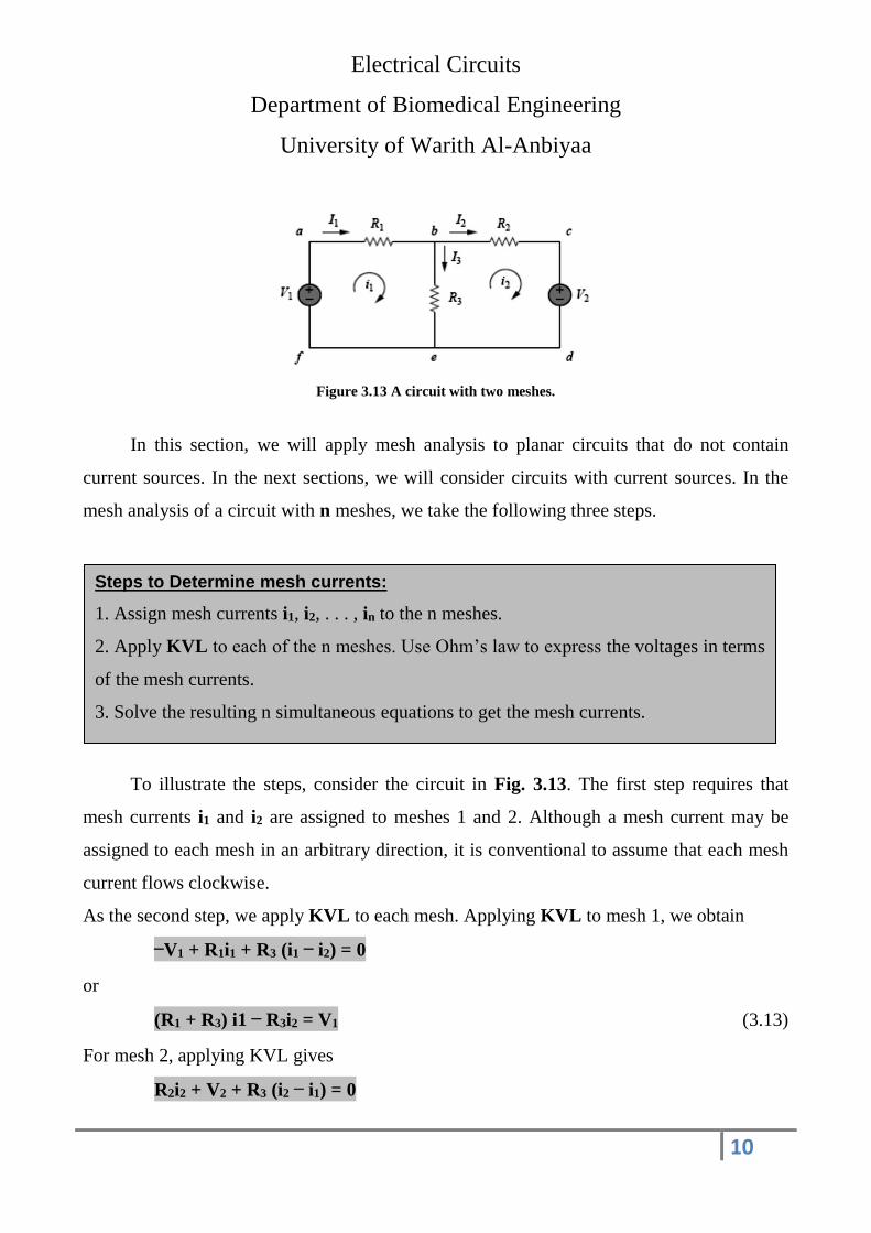
Figure 3.13 A circuit with two meshes.
In this section, we will apply mesh analysis to planar circuits that do not contain
current sources. In the next sections, we will consider circuits with current sources. In the
mesh analysis of a circuit with n meshes, we take the following three steps.
To illustrate the steps, consider the circuit in Fig. 3.13. The first step requires that
mesh currents i1 and i2 are assigned to meshes 1 and 2. Although a mesh current may be
assigned to each mesh in an arbitrary direction, it is conventional to assume that each mesh
current flows clockwise.
As the second step, we apply KVL to each mesh. Applying KVL to mesh 1, we obtain
−V1 + R1i1 + R3 (i1 − i2) = 0
or
(R1 + R3) i1 − R3i2 = V1 (3.13)
For mesh 2, applying KVL gives
R2i2 + V2 + R3 (i2 − i1) = 0
Steps to Determine mesh currents:
1. Assign mesh currents i1, i2, . . . , in to the n meshes.
2. Apply KVL to each of the n meshes. Use Ohm’s law to express the voltages in terms
of the mesh currents.
3. Solve the resulting n simultaneous equations to get the mesh currents.
Electrical Circuits
Department of Biomedical Engineering
University of Warith Al-Anbiyaa
11
or
−R3i1 + (R2 + R3) i2 = −V2 (3.14)
Note in Eq. (3.13) that the coefficient of i1 is the sum of the resistances in the first
mesh, while the coefficient of i2 is the negative of the resistance common to meshes 1 and 2.
Now observe that the same is true in Eq. (3.14). This can serve as a shortcut way of writing
the mesh equations.
The third step is to solve for the mesh currents. Putting Eqs. (3.13). and (3.14) in matrix
form yields
[𝑹𝟏 + 𝑹𝟑 −𝑹𝟑
−𝑹𝟑 𝑹𝟐 + 𝑹𝟑] [
𝒊𝟏
𝒊𝟐] = [
𝑽𝟏
−𝑽𝟐] (3.15)
which can be solved to obtain the mesh currents i1 and i2. We are at liberty to use any
technique for solving the simultaneous equations. If a circuit has n nodes, b branches, and l
independent loops or meshes, then l = b−n+1. Hence, l independent simultaneous equations
are required to solve the circuit using mesh analysis.
Notice that the branch currents are different from the mesh currents unless the mesh is
isolated. To distinguish between the two types of currents, we use i for a mesh current and I
for a branch current. The current elements I1, I2, and I3 are algebraic sums of the mesh
currents. It is evident from Fig. 3.13 that
I1 = i1, I2 = i2, I3 = i1 − i2 (3.16)
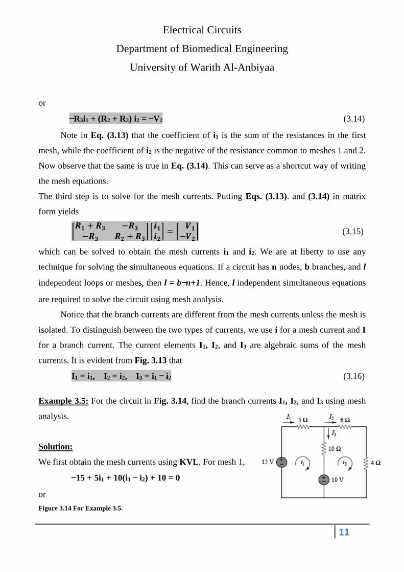
Example 3.5: For the circuit in Fig. 3.14, find the branch currents I1, I2, and I3 using mesh
analysis.
Solution:
We first obtain the mesh currents using KVL. For mesh 1,
−15 + 5i1 + 10(i1 − i2) + 10 = 0
or
Figure 3.14 For Example 3.5.
Electrical Circuits
Department of Biomedical Engineering
University of Warith Al-Anbiyaa
12
3i1 − 2i2 = 1 (3.5.1)
For mesh 2,
6i2 + 4i2 + 10(i2 − i1) − 10 = 0
or
i1 = 2i2 − 1 (3.5.2)
Using the substitution method, we substitute Eq. (3.5.2) into Eq. (3.5.1), and write
6i2 − 3 − 2i2 = 1 ⇒ i2 = 1 A
From Eq. (3.5.2), i1 = 2i2 − 1 = 2 − 1 = 1 A. Thus,
I1 = i1 = 1 A, I2 = i2 = 1 A, I3 = i1 − i2 = 0
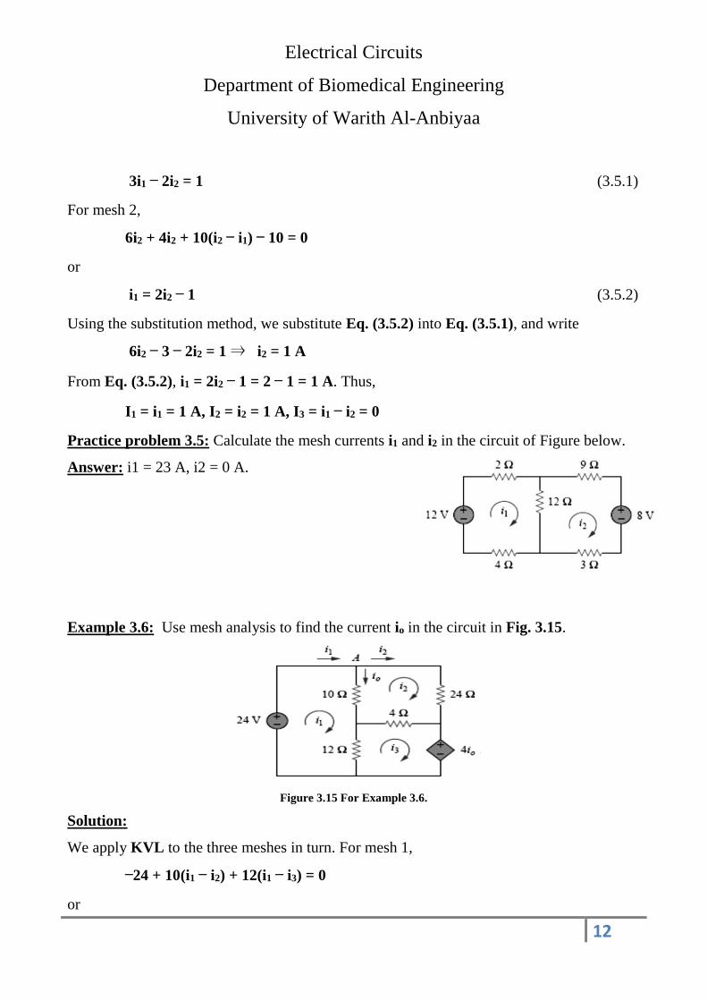
Practice problem 3.5: Calculate the mesh currents i1 and i2 in the circuit of Figure below.
Answer: i1 = 23 A, i2 = 0 A.
Example 3.6: Use mesh analysis to find the current io in the circuit in Fig. 3.15.
Figure 3.15 For Example 3.6.
Solution:
We apply KVL to the three meshes in turn. For mesh 1,
−24 + 10(i1 − i2) + 12(i1 − i3) = 0
or
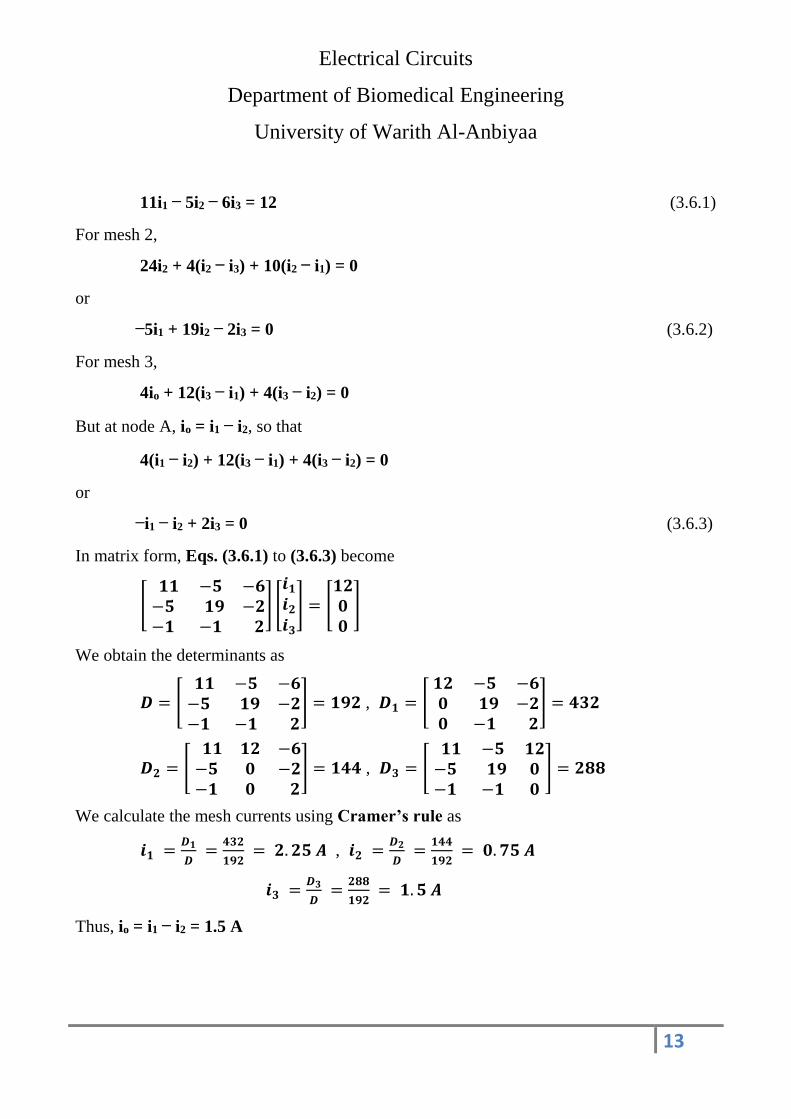
Electrical Circuits
Department of Biomedical Engineering
University of Warith Al-Anbiyaa
13
11i1 − 5i2 − 6i3 = 12 (3.6.1)
For mesh 2,
24i2 + 4(i2 − i3) + 10(i2 − i1) = 0
or
−5i1 + 19i2 − 2i3 = 0 (3.6.2)
For mesh 3,
4io + 12(i3 − i1) + 4(i3 − i2) = 0
But at node A, io = i1 − i2, so that
4(i1 − i2) + 12(i3 − i1) + 4(i3 − i2) = 0
or
−i1 − i2 + 2i3 = 0 (3.6.3)
In matrix form, Eqs. (3.6.1) to (3.6.3) become
[ 𝟏𝟏 −𝟓 −𝟔−𝟓 𝟏𝟗 −𝟐−𝟏 −𝟏 𝟐
] [
𝒊𝟏
𝒊𝟐
𝒊𝟑
] = [𝟏𝟐𝟎𝟎
]
We obtain the determinants as
𝑫 = [ 𝟏𝟏 −𝟓 −𝟔−𝟓 𝟏𝟗 −𝟐−𝟏 −𝟏 𝟐
] = 𝟏𝟗𝟐 , 𝑫𝟏 = [ 𝟏𝟐 −𝟓 −𝟔 𝟎 𝟏𝟗 −𝟐 𝟎 −𝟏 𝟐
] = 𝟒𝟑𝟐
𝑫𝟐 = [ 𝟏𝟏 𝟏𝟐 −𝟔−𝟓 𝟎 −𝟐−𝟏 𝟎 𝟐
] = 𝟏𝟒𝟒 , 𝑫𝟑 = [ 𝟏𝟏 −𝟓 𝟏𝟐−𝟓 𝟏𝟗 𝟎−𝟏 −𝟏 𝟎
] = 𝟐𝟖𝟖
We calculate the mesh currents using Cramer’s rule as
𝒊𝟏 =𝑫𝟏
𝑫 =
𝟒𝟑𝟐
𝟏𝟗𝟐 = 𝟐. 𝟐𝟓 𝑨 , 𝒊𝟐 =
𝑫𝟐
𝑫 =
𝟏𝟒𝟒
𝟏𝟗𝟐 = 𝟎. 𝟕𝟓 𝑨
𝒊𝟑 =𝑫𝟑
𝑫 =
𝟐𝟖𝟖
𝟏𝟗𝟐 = 𝟏. 𝟓 𝑨
Thus, io = i1 − i2 = 1.5 A
Electrical Circuits
Department of Biomedical Engineering
University of Warith Al-Anbiyaa
14
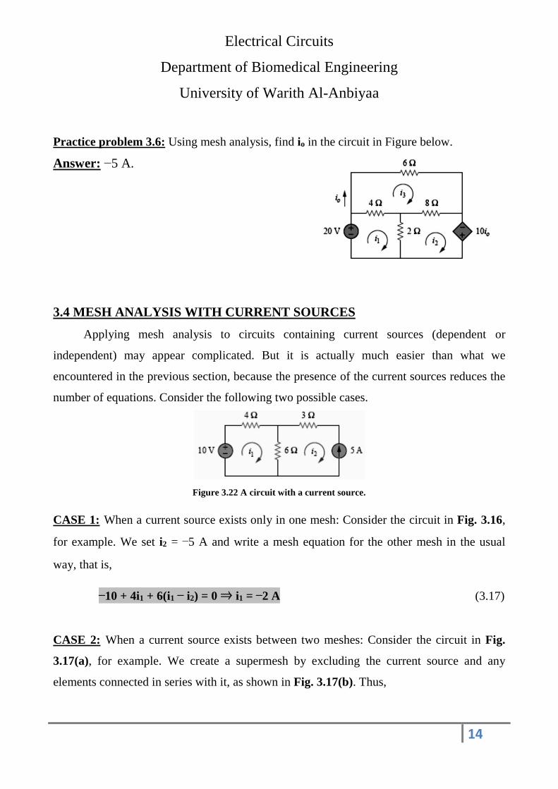
Practice problem 3.6: Using mesh analysis, find io in the circuit in Figure below.
Answer: −5 A.
3.4 MESH ANALYSIS WITH CURRENT SOURCES
Applying mesh analysis to circuits containing current sources (dependent or
independent) may appear complicated. But it is actually much easier than what we
encountered in the previous section, because the presence of the current sources reduces the
number of equations. Consider the following two possible cases.
Figure 3.22 A circuit with a current source.
CASE 1: When a current source exists only in one mesh: Consider the circuit in Fig. 3.16,
for example. We set i2 = −5 A and write a mesh equation for the other mesh in the usual
way, that is,
−10 + 4i1 + 6(i1 − i2) = 0 ⇒ i1 = −2 A (3.17)
CASE 2: When a current source exists between two meshes: Consider the circuit in Fig.
3.17(a), for example. We create a supermesh by excluding the current source and any
elements connected in series with it, as shown in Fig. 3.17(b). Thus,
Electrical Circuits
Department of Biomedical Engineering
University of Warith Al-Anbiyaa
15
A supermesh results when two meshes have a (dependent or independent) current
source in common.
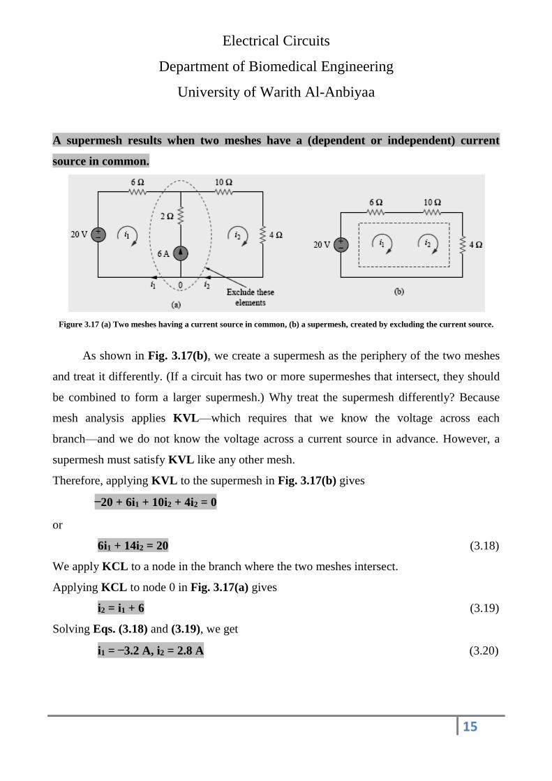
Figure 3.17 (a) Two meshes having a current source in common, (b) a supermesh, created by excluding the current source.
As shown in Fig. 3.17(b), we create a supermesh as the periphery of the two meshes
and treat it differently. (If a circuit has two or more supermeshes that intersect, they should
be combined to form a larger supermesh.) Why treat the supermesh differently? Because
mesh analysis applies KVL—which requires that we know the voltage across each
branch—and we do not know the voltage across a current source in advance. However, a
supermesh must satisfy KVL like any other mesh.
Therefore, applying KVL to the supermesh in Fig. 3.17(b) gives
−20 + 6i1 + 10i2 + 4i2 = 0
or
6i1 + 14i2 = 20 (3.18)
We apply KCL to a node in the branch where the two meshes intersect.
Applying KCL to node 0 in Fig. 3.17(a) gives
i2 = i1 + 6 (3.19)
Solving Eqs. (3.18) and (3.19), we get
i1 = −3.2 A, i2 = 2.8 A (3.20)
Electrical Circuits
Department of Biomedical Engineering
University of Warith Al-Anbiyaa
16
Note the following properties of a supermesh:
1. The current source in the supermesh is not completely ignored; it provides the constraint
equation necessary to solve for the mesh currents.
2. A supermesh has no current of its own.
3. A supermesh requires the application of both KVL and KCL.
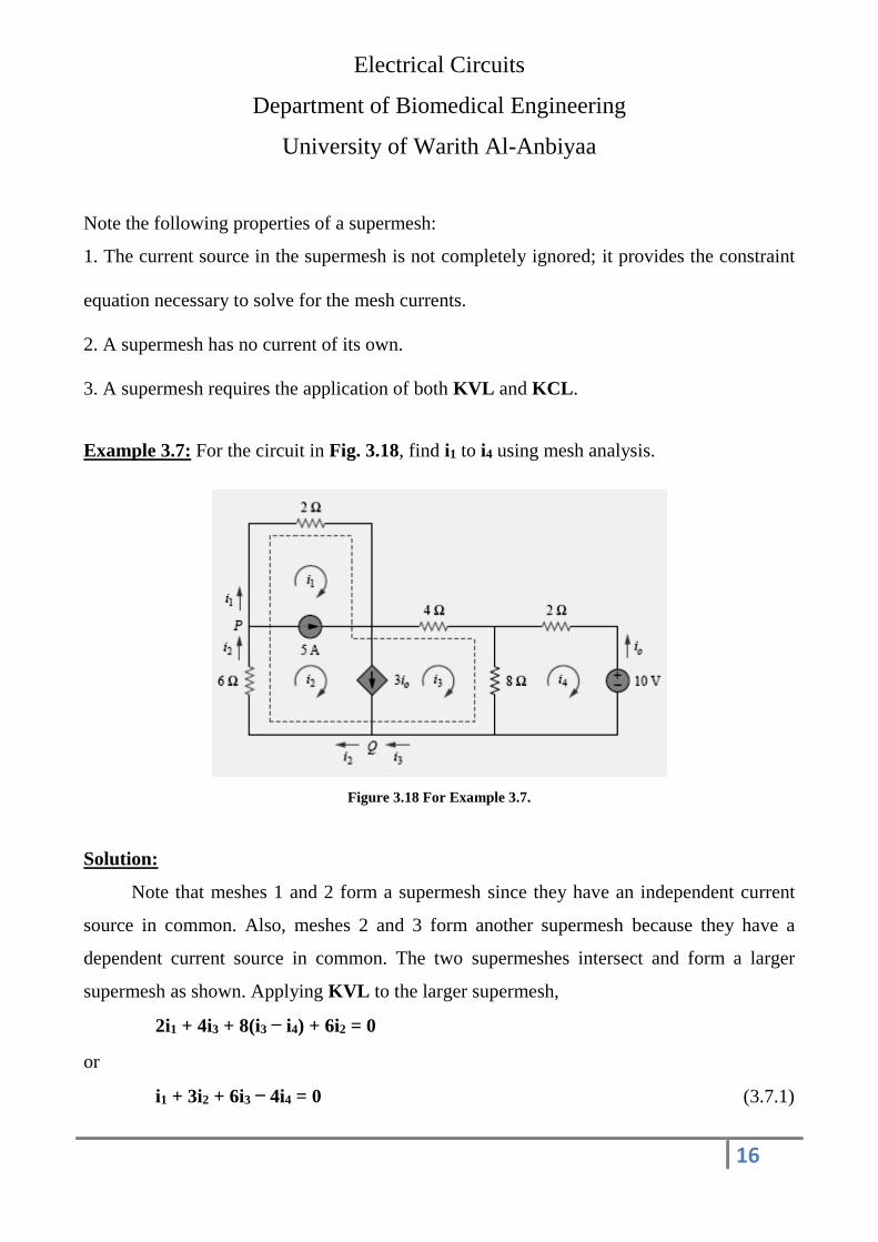
Example 3.7: For the circuit in Fig. 3.18, find i1 to i4 using mesh analysis.
Figure 3.18 For Example 3.7.
Solution:
Note that meshes 1 and 2 form a supermesh since they have an independent current
source in common. Also, meshes 2 and 3 form another supermesh because they have a
dependent current source in common. The two supermeshes intersect and form a larger
supermesh as shown. Applying KVL to the larger supermesh,
2i1 + 4i3 + 8(i3 − i4) + 6i2 = 0
or
i1 + 3i2 + 6i3 − 4i4 = 0 (3.7.1)
Electrical Circuits
Department of Biomedical Engineering
University of Warith Al-Anbiyaa
17
For the independent current source, we apply KCL to node P:
i2 = i1 + 5 (3.7.2)
For the dependent current source, we apply KCL to node Q:
i2 = i3 + 3io
But io = −i4, hence,
i2 = i3 − 3i4 (3.7.3)
Applying KVL in mesh 4,
2i4 + 8(i4 − i3) + 10 = 0
or
5i4 − 4i3 = −5 (3.7.4)
From Eqs. (3.7.1) to (3.7.4),
i1 = −7.5 A, i2 = −2.5 A, i3 = 3.93 A, i4 = 2.143 A
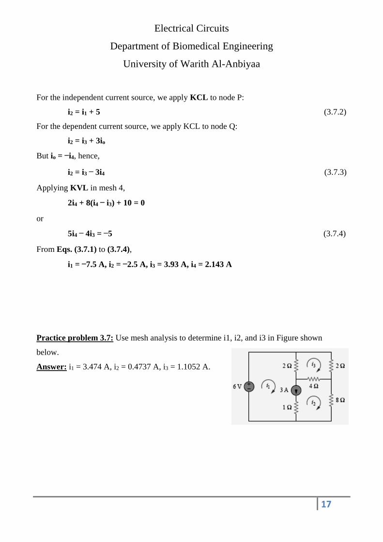
Practice problem 3.7: Use mesh analysis to determine i1, i2, and i3 in Figure shown
below.
Answer: i1 = 3.474 A, i2 = 0.4737 A, i3 = 1.1052 A.
Electrical Circuits
Department of Biomedical Engineering
University of Warith Al-Anbiyaa
18
3.5 NODAL ANALYSIS
Nodal analysis provides a general procedure for analyzing circuits using node
voltages as the circuit variables. Choosing node voltages instead of element voltages as
circuit variables is convenient and reduces the number of equations one must solve
simultaneously. To simplify matters, we shall assume in this section that circuits do not
contain voltage sources. Circuits that contain voltage sources will be analyzed in the next
section. In nodal analysis, we are interested in finding the node voltages. Given a circuit
with n nodes without voltage sources, the nodal analysis of the circuit involves taking the
following three steps.
We shall now explain and apply these three steps.
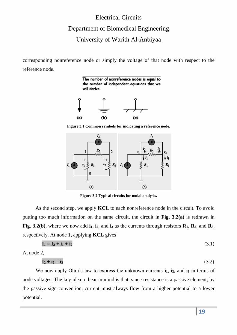
The first step in nodal analysis is selecting a node as the reference or datum node. The
reference node is commonly called the ground since it is assumed to have zero potential. A
reference node is indicated by any of the three symbols in Fig. 3.1. The type of ground in
Fig. 3.1(b) is called a chassis ground and is used in devices where the case, enclosure, or
chassis acts as a reference point for all circuits. When the potential of the earth is used as
reference, we use the earth ground in Fig. 3.1(a) or (c). We shall always use the symbol in
Fig. 3.1(b). Once we have selected a reference node, we assign voltage designations to
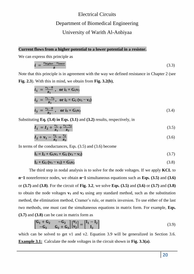
nonreference nodes. Consider, for example, the circuit in Fig. 3.2(a). Node 0 is the
reference node (v = 0), while nodes 1 and 2 are assigned voltages v1 and v2, respectively.
Keep in mind that the node voltages are defined with respect to the reference node. As
illustrated in Fig. 3.2(a), each node voltage is the voltage rise from the reference node to the
Steps to Determine Node Voltages:
1. Select a node as the reference node. Assign voltages v1, v2,. . vn−1 to the remaining n-1
nodes. The voltages are referenced with respect to the reference node.
2. Apply KCL to each of the n-1 nonreference nodes. Use Ohm’s law to express the branch
currents in terms of node voltages.
3. Solve the resulting simultaneous equations to obtain the unknown node voltages.
Electrical Circuits
Department of Biomedical Engineering
University of Warith Al-Anbiyaa
19
corresponding nonreference node or simply the voltage of that node with respect to the
reference node.
Figure 3.1 Common symbols for indicating a reference node.
Figure 3.2 Typical circuits for nodal analysis.
As the second step, we apply KCL to each nonreference node in the circuit. To avoid
putting too much information on the same circuit, the circuit in Fig. 3.2(a) is redrawn in
Fig. 3.2(b), where we now add i1, i2, and i3 as the currents through resistors R1, R2, and R3,
respectively. At node 1, applying KCL gives
I1 = I2 + i1 + i2 (3.1)
At node 2,
I2 + i2 = i3 (3.2)
We now apply Ohm’s law to express the unknown currents i1, i2, and i3 in terms of
node voltages. The key idea to bear in mind is that, since resistance is a passive element, by
the passive sign convention, current must always flow from a higher potential to a lower
potential.
Electrical Circuits
Department of Biomedical Engineering
University of Warith Al-Anbiyaa
20
Current flows from a higher potential to a lower potential in a resistor.
We can express this principle as
𝒊 = 𝒗𝒉𝒊𝒈𝒉𝒆𝒓 – 𝒗𝒍𝒐𝒘𝒆𝒓
𝑹 (3.3)
Note that this principle is in agreement with the way we defined resistance in Chapter 2 (see
Fig. 2.3). With this in mind, we obtain from Fig. 3.2(b),
𝒊𝟏 = 𝐯𝟏 – 𝟎
𝑹𝟏 , or i1 = G1v1
𝒊𝟐 = 𝐯𝟏 – 𝐯𝟐
𝑹𝟐 , or i2 = G2 (v1 − v2)
𝒊𝟑 = 𝐯𝟐 – 𝟎
𝑹𝟑 , or i3 = G3v2 (3.4)
Substituting Eq. (3.4) in Eqs. (3.1) and (3.2) results, respectively, in
𝑰𝟏 = 𝑰𝟐 + 𝐯𝟏
𝑹𝟏+
𝐯𝟏−𝐯𝟐
𝑹𝟐 (3.5)
𝑰𝟐 + 𝐯𝟏 − 𝐯𝟐
𝑹𝟐=
𝐯𝟐
𝑹𝟑 (3.6)
In terms of the conductances, Eqs. (3.5) and (3.6) become
I1 = I2 + G1v1 + G2 (v1 − v2) (3.7)
I2 + G2 (v1 − v2) = G3v2 (3.8)
The third step in nodal analysis is to solve for the node voltages. If we apply KCL to
n−1 nonreference nodes, we obtain n−1 simultaneous equations such as Eqs. (3.5) and (3.6)
or (3.7) and (3.8). For the circuit of Fig. 3.2, we solve Eqs. (3.5) and (3.6) or (3.7) and (3.8)
to obtain the node voltages v1 and v2 using any standard method, such as the substitution
method, the elimination method, Cramer’s rule, or matrix inversion. To use either of the last
two methods, one must cast the simultaneous equations in matrix form. For example, Eqs.
(3.7) and (3.8) can be cast in matrix form as
[𝐆𝟏 + 𝐆𝟐 −𝐆𝟐
−𝐆𝟐 𝐆𝟐 + 𝐆𝟑] [
𝐯𝟏
𝐯𝟐] = [
𝐈𝟏 − 𝐈𝟐
𝐈𝟐] (3.9)
which can be solved to get v1 and v2. Equation 3.9 will be generalized in Section 3.6.
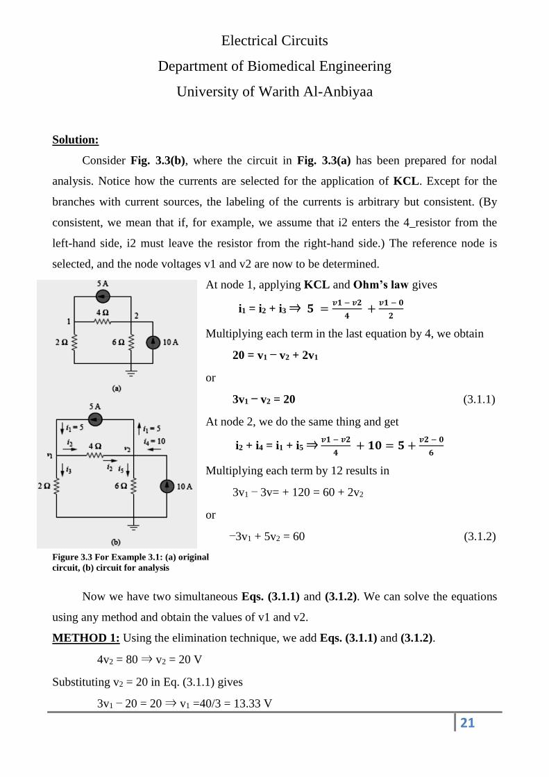
Example 3.1: Calculate the node voltages in the circuit shown in Fig. 3.3(a).
Electrical Circuits
Department of Biomedical Engineering
University of Warith Al-Anbiyaa
21
Solution:
Consider Fig. 3.3(b), where the circuit in Fig. 3.3(a) has been prepared for nodal
analysis. Notice how the currents are selected for the application of KCL. Except for the
branches with current sources, the labeling of the currents is arbitrary but consistent. (By
consistent, we mean that if, for example, we assume that i2 enters the 4_resistor from the
left-hand side, i2 must leave the resistor from the right-hand side.) The reference node is
selected, and the node voltages v1 and v2 are now to be determined.
At node 1, applying KCL and Ohm’s law gives
i1 = i2 + i3 ⇒ 𝟓 =𝒗𝟏 − 𝒗𝟐
𝟒 +
𝒗𝟏 − 𝟎
𝟐
Multiplying each term in the last equation by 4, we obtain
20 = v1 − v2 + 2v1
or
3v1 − v2 = 20 (3.1.1)
At node 2, we do the same thing and get
i2 + i4 = i1 + i5 ⇒ 𝒗𝟏 − 𝒗𝟐
𝟒 + 𝟏𝟎 = 𝟓 +
𝒗𝟐 − 𝟎
𝟔
Multiplying each term by 12 results in
3v1 − 3v= + 120 = 60 + 2v2
or
−3v1 + 5v2 = 60 (3.1.2)
Figure 3.3 For Example 3.1: (a) original
circuit, (b) circuit for analysis
Now we have two simultaneous Eqs. (3.1.1) and (3.1.2). We can solve the equations
using any method and obtain the values of v1 and v2.
METHOD 1: Using the elimination technique, we add Eqs. (3.1.1) and (3.1.2).
4v2 = 80 ⇒ v2 = 20 V
Substituting v2 = 20 in Eq. (3.1.1) gives
3v1 − 20 = 20 ⇒ v1 =40/3 = 13.33 V
Electrical Circuits
Department of Biomedical Engineering
University of Warith Al-Anbiyaa
22
METHOD 2: To use Cramer’s rule, we need to put Eqs. (3.1.1) and (3.1.2) in matrix form
as
[ 3 −1−3 5
] [𝑣1
𝑣2] = [
2060
] (3.1.3)
The determinant of the matrix is
𝛥 = 𝐷 = | 3 −1−3 5
| = 15 − 3 = 12
We now obtain v1 and v2 as
𝒗𝟏 =𝐷1
𝐷=
|20 −160 5
|
𝐷=
100+60
12= 13.33𝑉
𝒗𝟐 =𝐷2
𝐷=
| 3 20−3 60
|
𝐷=
180+60
12= 20𝑉
giving us the same result as did the elimination method.
If we need the currents, we can easily calculate them from the values of the nodal voltages.
i1 = 5 A, 𝒊𝟐 =𝒗𝟏 − 𝒗𝟐
𝟒 = −𝟏. 𝟔𝟔𝟔𝟕 𝑨, 𝒊𝟑 =
𝒗𝟏
𝟐 = 𝟔. 𝟔𝟔𝟔𝑨,
i4 = 10 A, 𝒊𝟓 =𝒗𝟐
𝟔 = 𝟑. 𝟑𝟑𝟑𝑨
The fact that i2 is negative shows that the current flows in the direction opposite to the
one assumed.
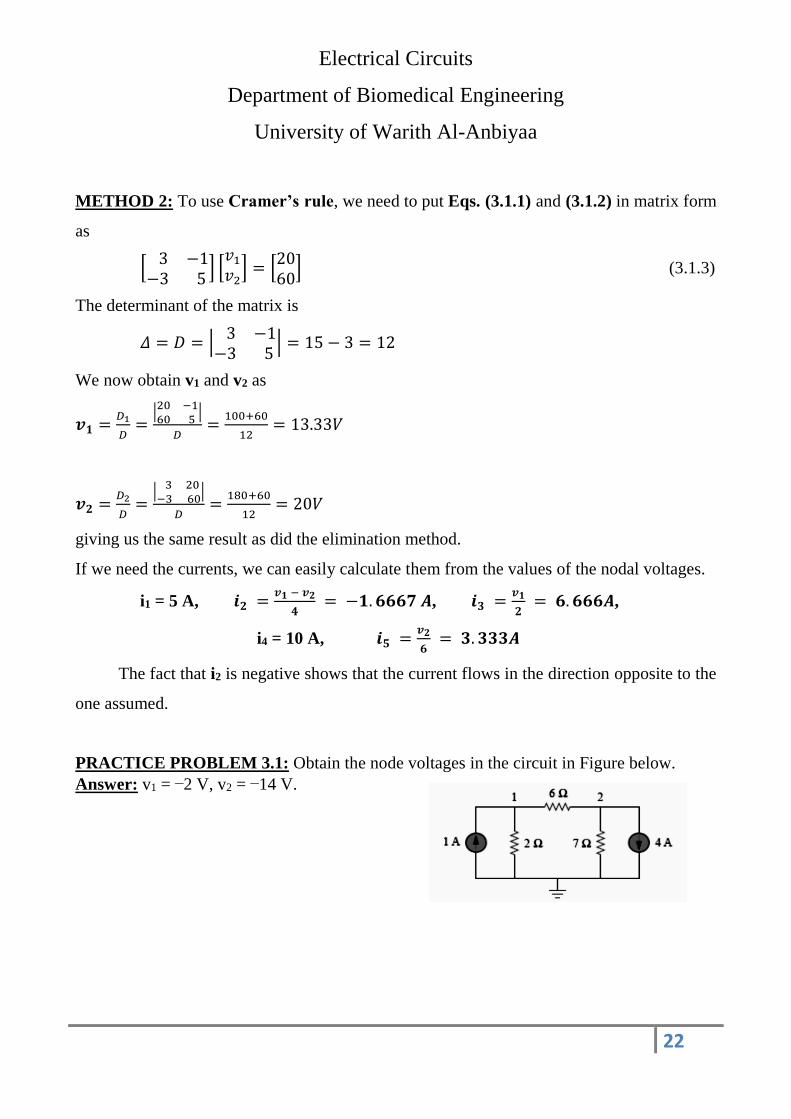
PRACTICE PROBLEM 3.1: Obtain the node voltages in the circuit in Figure below.
Answer: v1 = −2 V, v2 = −14 V.
Electrical Circuits
Department of Biomedical Engineering
University of Warith Al-Anbiyaa
23
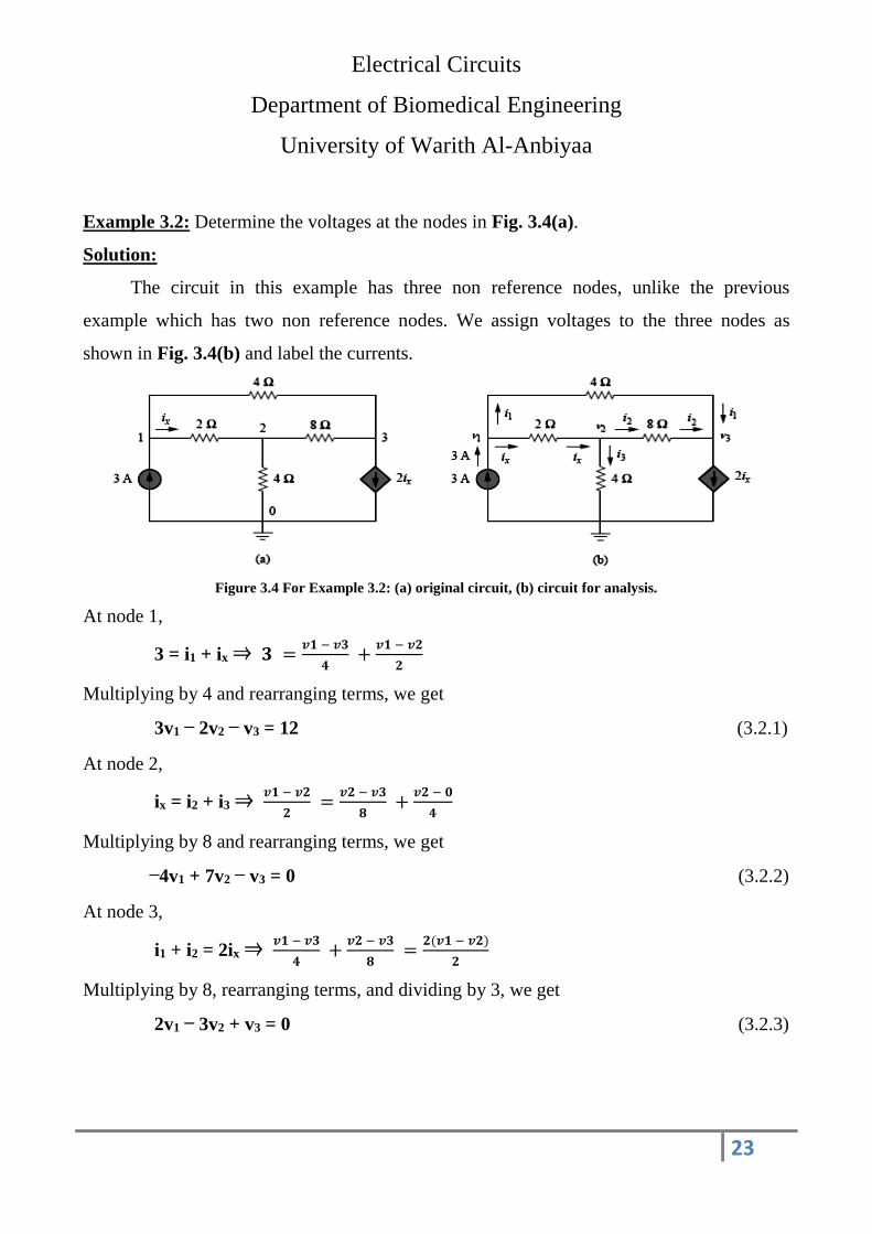
Example 3.2: Determine the voltages at the nodes in Fig. 3.4(a).
Solution:
The circuit in this example has three non reference nodes, unlike the previous
example which has two non reference nodes. We assign voltages to the three nodes as
shown in Fig. 3.4(b) and label the currents.
Figure 3.4 For Example 3.2: (a) original circuit, (b) circuit for analysis.
At node 1,
3 = i1 + ix ⇒ 𝟑 =𝒗𝟏 − 𝒗𝟑
𝟒 +
𝒗𝟏 − 𝒗𝟐
𝟐
Multiplying by 4 and rearranging terms, we get
3v1 − 2v2 − v3 = 12 (3.2.1)
At node 2,
ix = i2 + i3 ⇒ 𝒗𝟏 − 𝒗𝟐
𝟐 =
𝒗𝟐 − 𝒗𝟑
𝟖 +
𝒗𝟐 − 𝟎
𝟒
Multiplying by 8 and rearranging terms, we get
−4v1 + 7v2 − v3 = 0 (3.2.2)
At node 3,
i1 + i2 = 2ix ⇒ 𝒗𝟏 − 𝒗𝟑
𝟒 +
𝒗𝟐 − 𝒗𝟑
𝟖 =
𝟐(𝒗𝟏 − 𝒗𝟐)
𝟐
Multiplying by 8, rearranging terms, and dividing by 3, we get
2v1 − 3v2 + v3 = 0 (3.2.3)
Electrical Circuits
Department of Biomedical Engineering
University of Warith Al-Anbiyaa
24
We have three simultaneous equations to solve to get the node voltages v1, v2, and v3.
We shall solve the equations in Cramer’s rule ways. We will put Eqs. (3.2.1) to (3.2.3) in
matrix form.
[ 3 −2 −1−4 7 −1 2 −3 1
] [
𝑣1
𝑣2
𝑣3
] = [1200
]
From this, we obtain
𝒗𝟏 =𝑫𝟏
𝑫, 𝒗𝟐 =
𝑫𝟐
𝑫, 𝒗𝟑 =
𝑫𝟑
𝑫
where D, D1, D2, and D3 are the determinants to be calculated as follows.
𝐷 = | 3 −2 −1−4 7 −1 2 −3 1
| = 21 − 12 + 4 + 14 − 9 − 8 = 10
Similarly, we obtain
𝐷1 = |12 −2 −10 7 −10 −3 1
| = 84 + 0 + 0 − 0 − 36 − 0 = 48
𝐷2 = | 3 12 −1−4 0 −1 2 0 1
| = 0 + 0 − 24 − 0 − 0 + 48 = 24
𝐷3 = | 3 −2 12−4 7 0 2 −3 0
| = 0 + 144 + 0 − 168 − 0 − 0 = −24
Thus, we find
𝒗𝟏 =𝑫𝟏
𝑫 =
𝟒𝟖
𝟏𝟎 = 𝟒. 𝟖 𝑽, 𝒗𝟐 =
𝑫𝟐
𝑫 =
𝟐𝟒
𝟏𝟎 = 𝟐. 𝟒 𝑽
𝒗𝟑 =𝑫𝟑
𝑫 =
−𝟐𝟒
𝟏𝟎 = −𝟐. 𝟒 𝑽
Electrical Circuits
Department of Biomedical Engineering
University of Warith Al-Anbiyaa
25
Practice problem 3.2: Find the voltages at the three nonreference nodes in the circuit of
Figure below.
Answer: v1 = 80 V, v2 = −64 V, v3 = 156 V.
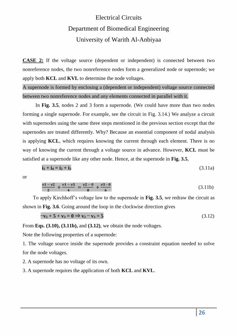
3.6 NODAL ANALYSIS WITH VOLTAGE SOURCES
We now consider how voltage sources affect nodal analysis. We use the circuit in Fig.
3.5 for illustration. Consider the following two possibilities.
CASE 1: If a voltage source is connected between the reference node and a nonreference
node, we simply set the voltage at the nonreference node equal to the voltage of the voltage
source. In Fig. 3.5, for example,
v1 = 10 V (3.10)
Thus our analysis is somewhat simplified by this knowledge of the voltage at this node.
Figure 3.5 A circuit with a supernode.
Electrical Circuits
Department of Biomedical Engineering
University of Warith Al-Anbiyaa
26
CASE 2: If the voltage source (dependent or independent) is connected between two
nonreference nodes, the two nonreference nodes form a generalized node or supernode; we
apply both KCL and KVL to determine the node voltages.
A supernode is formed by enclosing a (dependent or independent) voltage source connected
between two nonreference nodes and any elements connected in parallel with it.
In Fig. 3.5, nodes 2 and 3 form a supernode. (We could have more than two nodes
forming a single supernode. For example, see the circuit in Fig. 3.14.) We analyze a circuit
with supernodes using the same three steps mentioned in the previous section except that the
supernodes are treated differently. Why? Because an essential component of nodal analysis
is applying KCL, which requires knowing the current through each element. There is no
way of knowing the current through a voltage source in advance. However, KCL must be
satisfied at a supernode like any other node. Hence, at the supernode in Fig. 3.5,
i1 + i4 = i2 + i3 (3.11a)
or
𝒗𝟏 − 𝒗𝟐
𝟐 +
𝒗𝟏 − 𝒗𝟑
𝟒 =
𝒗𝟐 − 𝟎
𝟖 +
𝒗𝟑 – 𝟎
𝟔 (3.11b)
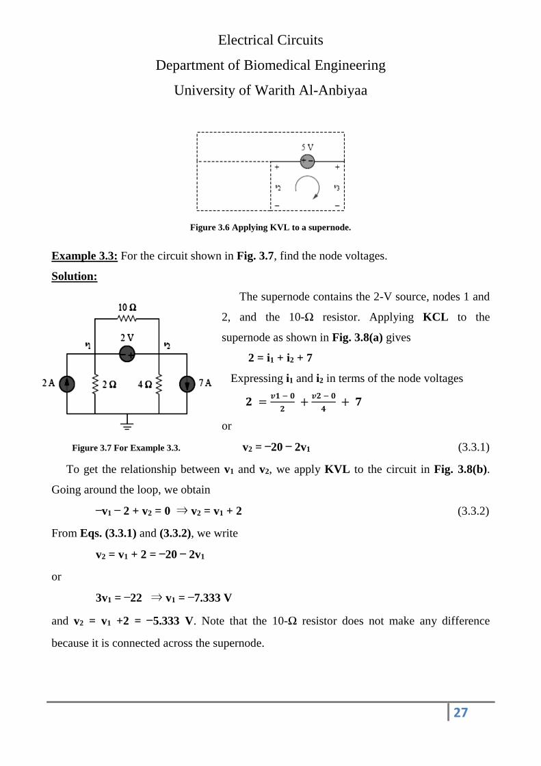
To apply Kirchhoff’s voltage law to the supernode in Fig. 3.5, we redraw the circuit as
shown in Fig. 3.6. Going around the loop in the clockwise direction gives
−v2 + 5 + v3 = 0 ⇒ v2 − v3 = 5 (3.12)
From Eqs. (3.10), (3.11b), and (3.12), we obtain the node voltages.
Note the following properties of a supernode:
1. The voltage source inside the supernode provides a constraint equation needed to solve
for the node voltages.
2. A supernode has no voltage of its own.
3. A supernode requires the application of both KCL and KVL.
Electrical Circuits
Department of Biomedical Engineering
University of Warith Al-Anbiyaa
27
Figure 3.6 Applying KVL to a supernode.
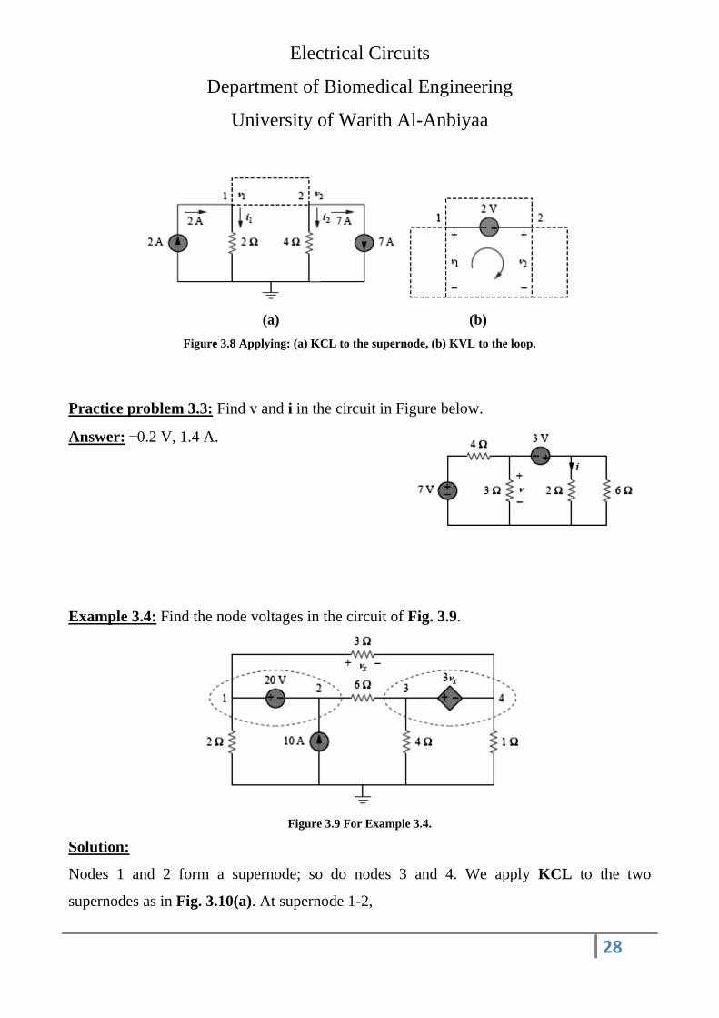
Example 3.3: For the circuit shown in Fig. 3.7, find the node voltages.
Solution:
The supernode contains the 2-V source, nodes 1 and
2, and the 10-Ω resistor. Applying KCL to the
supernode as shown in Fig. 3.8(a) gives
2 = i1 + i2 + 7
Expressing i1 and i2 in terms of the node voltages
𝟐 =𝒗𝟏 − 𝟎
𝟐 +
𝒗𝟐 − 𝟎
𝟒 + 𝟕
or
Figure 3.7 For Example 3.3. v2 = −20 − 2v1 (3.3.1)
To get the relationship between v1 and v2, we apply KVL to the circuit in Fig. 3.8(b).
Going around the loop, we obtain
−v1 − 2 + v2 = 0 ⇒ v2 = v1 + 2 (3.3.2)
From Eqs. (3.3.1) and (3.3.2), we write
v2 = v1 + 2 = −20 − 2v1
or
3v1 = −22 ⇒ v1 = −7.333 V
and v2 = v1 +2 = −5.333 V. Note that the 10-Ω resistor does not make any difference
because it is connected across the supernode.
Electrical Circuits
Department of Biomedical Engineering
University of Warith Al-Anbiyaa
28
(a) (b)
Figure 3.8 Applying: (a) KCL to the supernode, (b) KVL to the loop.
Practice problem 3.3: Find v and i in the circuit in Figure below.
Answer: −0.2 V, 1.4 A.
Example 3.4: Find the node voltages in the circuit of Fig. 3.9.
Figure 3.9 For Example 3.4.
Solution:
Nodes 1 and 2 form a supernode; so do nodes 3 and 4. We apply KCL to the two
supernodes as in Fig. 3.10(a). At supernode 1-2,
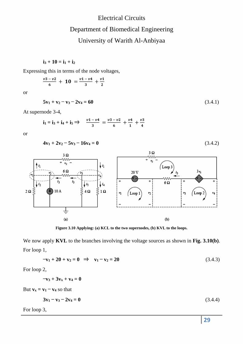
Electrical Circuits
Department of Biomedical Engineering
University of Warith Al-Anbiyaa
29
i3 + 10 = i1 + i2
Expressing this in terms of the node voltages,
𝒗𝟑 − 𝒗𝟐
𝟔 + 𝟏𝟎 =
𝒗𝟏 − 𝒗𝟒
𝟑 +
𝒗𝟏
𝟐
or
5v1 + v2 − v3 − 2v4 = 60 (3.4.1)
At supernode 3-4,
i1 = i3 + i4 + i5 ⇒ 𝒗𝟏 − 𝒗𝟒
𝟑 =
𝒗𝟑 − 𝒗𝟐
𝟔 +
𝒗𝟒
𝟏 +
𝒗𝟑
𝟒
or
4v1 + 2v2 − 5v3 − 16v4 = 0 (3.4.2)
Figure 3.10 Applying: (a) KCL to the two supernodes, (b) KVL to the loops.
We now apply KVL to the branches involving the voltage sources as shown in Fig. 3.10(b).
For loop 1,
−v1 + 20 + v2 = 0 ⇒ v1 − v2 = 20 (3.4.3)
For loop 2,
−v3 + 3vx + v4 = 0
But vx = v1 − v4 so that
3v1 − v3 − 2v4 = 0 (3.4.4)
For loop 3,
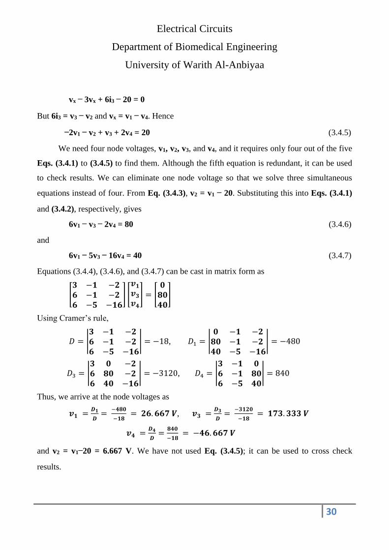
Electrical Circuits
Department of Biomedical Engineering
University of Warith Al-Anbiyaa
30
vx − 3vx + 6i3 − 20 = 0
But 6i3 = v3 − v2 and vx = v1 − v4. Hence
−2v1 − v2 + v3 + 2v4 = 20 (3.4.5)
We need four node voltages, v1, v2, v3, and v4, and it requires only four out of the five
Eqs. (3.4.1) to (3.4.5) to find them. Although the fifth equation is redundant, it can be used
to check results. We can eliminate one node voltage so that we solve three simultaneous
equations instead of four. From Eq. (3.4.3), v2 = v1 − 20. Substituting this into Eqs. (3.4.1)
and (3.4.2), respectively, gives
6v1 − v3 − 2v4 = 80 (3.4.6)
and
6v1 − 5v3 − 16v4 = 40 (3.4.7)
Equations (3.4.4), (3.4.6), and (3.4.7) can be cast in matrix form as
[𝟑 −𝟏 −𝟐𝟔 −𝟏 −𝟐𝟔 −𝟓 −𝟏𝟔
] [
𝒗𝟏
𝒗𝟑
𝒗𝟒
] = [𝟎
𝟖𝟎𝟒𝟎
]
Using Cramer’s rule,
𝐷 = |𝟑 −𝟏 −𝟐𝟔 −𝟏 −𝟐𝟔 −𝟓 −𝟏𝟔
| = −18, 𝐷1 = |𝟎 −𝟏 −𝟐
𝟖𝟎 −𝟏 −𝟐𝟒𝟎 −𝟓 −𝟏𝟔
| = −480
𝐷3 = |𝟑 𝟎 −𝟐𝟔 𝟖𝟎 −𝟐𝟔 𝟒𝟎 −𝟏𝟔
| = −3120, 𝐷4 = |𝟑 −𝟏 𝟎𝟔 −𝟏 𝟖𝟎𝟔 −𝟓 𝟒𝟎
| = 840
Thus, we arrive at the node voltages as
𝒗𝟏 =𝑫𝟏
𝑫=
−𝟒𝟖𝟎
−𝟏𝟖 = 𝟐𝟔. 𝟔𝟔𝟕 𝑽, 𝒗𝟑 =
𝑫𝟑
𝑫=
−𝟑𝟏𝟐𝟎
−𝟏𝟖 = 𝟏𝟕𝟑. 𝟑𝟑𝟑 𝑽
𝒗𝟒 =𝑫𝟒
𝑫=
𝟖𝟒𝟎
−𝟏𝟖 = −𝟒𝟔. 𝟔𝟔𝟕 𝑽
and v2 = v1−20 = 6.667 V. We have not used Eq. (3.4.5); it can be used to cross check
results.
Electrical Circuits
Department of Biomedical Engineering
University of Warith Al-Anbiyaa
31
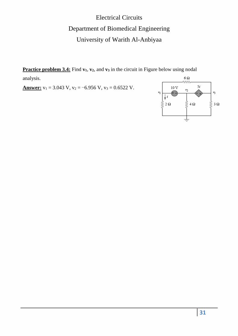
Practice problem 3.4: Find v1, v2, and v3 in the circuit in Figure below using nodal
analysis.
Answer: v1 = 3.043 V, v2 = −6.956 V, v3 = 0.6522 V.