Embed Size (px)
Citation preview
Electrical Design for Manufacturability Solutions:
Fast Systematic Variation Analysis and Design
Enhancement Techniques
by
Rami Fathy Amin Gomaa Salem
A thesispresented to the University of Waterloo
in fulfillment of thethesis requirement for the degree of
Doctor of Philosophyin
Electrical and Computer Engineering
Waterloo, Ontario, Canada, 2011
c© Rami Fathy Amin Gomaa Salem 2011

I hereby declare that I am the sole author of this thesis. This is a true copy of the thesis,including any required final revisions, as accepted by my examiners.
I understand that my thesis may be made electronically available to the public.
ii
Abstract
Since the scaling of physical dimensions has been faster than the optical wavelengthsor equipment tolerances in the manufacturing line, process variability has significantlyincreased. This, in turn, has led to unreliable design, unpredictable manufacturing, andlow yields. The results of these physical variations are circuit metric variations such asperformance and power, known as the parametric yield.
Source of variations are either systematic (for example, metal dishing and lithographicproximity effects) or random (for example, material variations and dopant fluctuations).The former can be modeled and predicted, whereas the random variations are inherentlyunpredictable. There are several pattern-dependent process effects which are systematicin nature. These can be detected and compensated for during the physical design to aidmanufacturability, and hence improve yield. This thesis focuses on ways to mitigate theimpact of systematic variations on design and manufacturing by establishing a bidirectionallink between the two. The motivation for doing so is to reduce design guardband and cost,and improve manufacturability and yield.
The primary objectives in this research are to develop computer-aided design (CAD)tools for Design for Manufacturability (DFM) solutions that enable designers to conductmore rapid and more accurate systematic variation analysis, with different design enhance-ment techniques. Four main CAD tools are developed throughout my thesis. The firstCAD tool facilitates a quantitative study of the impact of systematic variations for dif-ferent circuits’ electrical and geometrical behavior. This is accomplished by automaticallyperforming an extensive analysis of different process variations (lithography and stress)and their dependency on the design context. Such a tool helps to explore and evaluatethe systematic variation impact on any type of design (analog or digital, very dense or lessdense, large chips or small ones, and technology ”A” versus technology ”B”).
Secondly, solutions in the industry focus on the ”design and then fix philosophy”, or”fix during design philosophy”, whereas the next CAD tool involves the ”fix before designphilosophy”. Here, the standard cell library is characterized in different design contexts,different resolution enhancement techniques, and different process conditions, generating afully DFM-aware standard cell library using a newly developed methodology that dramati-cally reduce the required number of silicon simulations. Several experiments are conductedon 65nm and 45nm designs, and demonstrate more robust and manufacturable designs thatcan be implemented by using the DFM-aware standard cell library.
Thirdly, a novel electrical-aware hotspot detection solution, is developed by using adevice parameter-based matching technique since the state-of-the-art hotspot detection
iii

solutions are all geometrical based. This CAD tool proposes a new philosophy by detect-ing yield limiters, also known as hotspots, through the model parameters of the device,presented in the SPICE netlist. The device model parameters contain different abstractsof information such as the layout geometry, design context, and proximity effect on theprocess variability. This novel hotspot detection methodology is tested and delivers ex-traordinary fast and accurate results.
Finally, the existing DFM solutions that are focused on analyzing and detecting theelectrical variations, mainly address the digital designs. Process variations play an in-creasingly important role in the success of analog circuits. Knowledge of the parametervariances and their contribution patterns is crucial for a successful design process. Thisinformation is valuable to find solutions for many problems in design, design automation,testing, and fault tolerance. The fourth CAD solution, proposed in this thesis, introducesa variability-aware DFM solution that detects, analyze, and automatically correct hotspotsfor analog circuits.
This thesis presents high performance and novel design-aware process variation classi-fication and detection solutions along with automated design enhancement and correctiontechniques.
iv

Acknowledgements
I would like to give my sincere appreciation to my academic and professional ancestry Prof. Mo-hab Anis for his assistance, support, vision, and strong encouragement throughout my research.His insights and leadership in the semiconductor manufacturing academia have led me to theinteresting research topics. I would also like to thank Prof. David Nairn for accepting to be myco-supervisor and providing the tremendous support in facilitating my PhD. In addition to hisvaluable technical feedback on my research.
I would like to thank Professor Azadeh Davoodi for accepting to be the external examiner inmy PhD defense and I appreciate her time, and effort for traveling and her valuable comments onthis research . Also I would like to thank Professor Karim Karim, Professor Kumaraswamy Pon-nambalam and Professor Selvakumar Chettypalayam for serving on my PhD defense committeeand their valuable comments on this research.
I am very appreciative of the support from all of my colleagues at Mentor Graphics. In partic-ular, I would like to express my gratitude to Haitham Eissa, Mohamed Al-Imam, Ahmed Arafa,Hesham Abdulghany, Tamer AbdelRahim, Sherif Hammouda, Nader Hindawy, Sherif Hany, andAbdel Rahman El-Mously for their technical leadership and support.
My stay at University of Waterloo was stimulating and entertaining, thanks to the friendshipof Hassan Hassan, Mohamed AbuRahma, Ahmed Youssef, Muhammad Nummer, Aymen Ismail,Noman Hai, Hazem Shehata and many other friends.
All of this was only made possible by the encouragement and love of my family. My deepestgratitude goes to my mother and father for their never ending support, and for remembering mein their prayers. No words of appreciation could ever reward them for all they have done for me.I am, and will ever be, indebted to them for all the achievements in my life. I am also thankfulto my siblings Tamer,and Sally for their endless support. My loving wife, Marwa, shared withme every moment of my Ph.D. She supported me with her unconditional love and care duringall the ups and downs of my research, and she was always there to motivate me. I thank her foreverything she have done.
Finally, I express my gratitude to Allah (God) for providing me the blessings and strength tocomplete this work.
Rami Fathy Amin Gomaa SalemJuly, 2011
v

Dedication
To my Mother and Father, for their invaluable prayers. To my wife Marwa, for herboundless love that inspires me to become a better man, for supporting my completion ofthis thesis, for being my emotional rock in times of doubt. To my beloved children Zeina
and Marwan
vi
Contents
List of Tables xi
List of Figures xii
1 Introduction and Motivation 1
1.1 Introduction . . . . . . . . . . . . . . . . . . . . . . . . . . . . . . . . . . . 1
1.2 Motivation: DFM Solutions for Parametric Yield . . . . . . . . . . . . . . 2
1.3 Thesis Outline . . . . . . . . . . . . . . . . . . . . . . . . . . . . . . . . . . 3
1.4 Thesis Contributions . . . . . . . . . . . . . . . . . . . . . . . . . . . . . . 4
2 Background: Process Variations and DFM Solutions 7
2.1 Introduction . . . . . . . . . . . . . . . . . . . . . . . . . . . . . . . . . . . 7
2.2 Sources of Process Variations . . . . . . . . . . . . . . . . . . . . . . . . . 8
2.2.1 Sources of Systematic Variations: Optical Lithography . . . . . . . 9
2.2.2 Sources of Systematic Variations: Chemical Mechanical Polishing . 14
2.2.3 Sources of Systematic Variations: Mechanical Stress . . . . . . . . . 16
2.2.4 Sources of Systematic Variations: Material Dopping . . . . . . . . . 17
2.3 Yield Issues Due to Process Variations . . . . . . . . . . . . . . . . . . . . 18
2.3.1 Impact of Process Variations on Parametric yield . . . . . . . . . . 19
2.4 Design for Manufacturing . . . . . . . . . . . . . . . . . . . . . . . . . . . 26
2.4.1 Traditional DFM Methods . . . . . . . . . . . . . . . . . . . . . . . 26
vii
2.4.2 Taxonomy . . . . . . . . . . . . . . . . . . . . . . . . . . . . . . . . 28
2.5 Summary . . . . . . . . . . . . . . . . . . . . . . . . . . . . . . . . . . . . 36
3 A Methodology for Analyzing Process Variation Dependency on DesignContext and the Impact on Circuit Analysis 37
3.1 Introduction . . . . . . . . . . . . . . . . . . . . . . . . . . . . . . . . . . . 37
3.2 Background . . . . . . . . . . . . . . . . . . . . . . . . . . . . . . . . . . . 39
3.2.1 Corners Simulation . . . . . . . . . . . . . . . . . . . . . . . . . . . 39
3.2.2 Monte Carlo Analysis . . . . . . . . . . . . . . . . . . . . . . . . . . 40
3.2.3 Response Surface Modeling . . . . . . . . . . . . . . . . . . . . . . 40
3.2.4 Issues with the Previous Process Analysis Tools . . . . . . . . . . . 41
3.3 Design Context Impact on Process Variations . . . . . . . . . . . . . . . . 42
3.3.1 Design Context Impact on Lithography Variations . . . . . . . . . . 42
3.3.2 Design Context Impact on Stress Variations . . . . . . . . . . . . . 43
3.4 Characterization Flow: Layout Design Context Impact on Lithography andStress Variations . . . . . . . . . . . . . . . . . . . . . . . . . . . . . . . . 44
3.4.1 Context Generator Engine . . . . . . . . . . . . . . . . . . . . . . . 44
3.5 Experiments and Results . . . . . . . . . . . . . . . . . . . . . . . . . . . . 48
3.5.1 Layout Design Context Effect on Standard Cells’ Geometrical Level 48
3.5.2 Layout Design Context Effect on Standard Cells’ Electrical Level . 49
3.5.3 Systematic Variations Impact on Ring Oscillator designed at 65nm 55
3.6 Summary . . . . . . . . . . . . . . . . . . . . . . . . . . . . . . . . . . . . 59
4 Fix Before Design CAD Solution: DFM-aware Standard Cell Re-characterization 60
4.1 Introduction . . . . . . . . . . . . . . . . . . . . . . . . . . . . . . . . . . . 60
4.2 Background . . . . . . . . . . . . . . . . . . . . . . . . . . . . . . . . . . . 61
4.3 DFM-aware standard cell re-characterization flow . . . . . . . . . . . . . . 62
4.3.1 Isolated Process Point Engine (IPPE) . . . . . . . . . . . . . . . . . 64
4.4 Experiments and Results . . . . . . . . . . . . . . . . . . . . . . . . . . . . 72
viii

4.4.1 Standard cell library re-characterization . . . . . . . . . . . . . . . 72
4.4.2 DFM-aware Finite Impulse Response (FIR) filter designed at 45nm 76
4.5 Summary . . . . . . . . . . . . . . . . . . . . . . . . . . . . . . . . . . . . 80
5 High Performance Electrical Driven Hotspot Detection CAD Solution forFull Chip Design using a Novel Device Parameter Matching Technique 82
5.1 Introduction . . . . . . . . . . . . . . . . . . . . . . . . . . . . . . . . . . . 82
5.2 Background . . . . . . . . . . . . . . . . . . . . . . . . . . . . . . . . . . . 83
5.2.1 Rule-based Hotspot Detection . . . . . . . . . . . . . . . . . . . . . 83
5.2.2 Model/Simulation-based Hotspot Detection . . . . . . . . . . . . . 84
5.2.3 Pattern Matching-based Hotspot Detection . . . . . . . . . . . . . . 84
5.2.4 Electrical-driven Hotspot Detection . . . . . . . . . . . . . . . . . . 85
5.3 Proposed Flow Overview: Design and Electrical Driven Hotspot Detectionsolution . . . . . . . . . . . . . . . . . . . . . . . . . . . . . . . . . . . . . 87
5.3.1 Smart Device Parameters Matching Engine . . . . . . . . . . . . . . 91
5.3.2 Intent Driven Design Engine . . . . . . . . . . . . . . . . . . . . . . 94
5.4 Experiments and Results . . . . . . . . . . . . . . . . . . . . . . . . . . . . 96
5.4.1 Accuracy of the proposed solution . . . . . . . . . . . . . . . . . . . 96
5.4.2 Runtime Analysis . . . . . . . . . . . . . . . . . . . . . . . . . . . . 100
5.5 Summary . . . . . . . . . . . . . . . . . . . . . . . . . . . . . . . . . . . . 101
6 A Parametric DFM CAD Solution for Analog Circuits: Electrical DrivenHot Spot Detection, Analysis and Correction Flow 102
6.1 Introduction . . . . . . . . . . . . . . . . . . . . . . . . . . . . . . . . . . . 102
6.2 Background . . . . . . . . . . . . . . . . . . . . . . . . . . . . . . . . . . . 103
6.3 Proposed Flow Overview: Electrical Hot Spot Detection, Analysis and Cor-rection Flow . . . . . . . . . . . . . . . . . . . . . . . . . . . . . . . . . . . 105
6.3.1 Intent Driven Design Engine . . . . . . . . . . . . . . . . . . . . . . 109
6.3.2 E-hotspot Detection Engine . . . . . . . . . . . . . . . . . . . . . . 110
ix
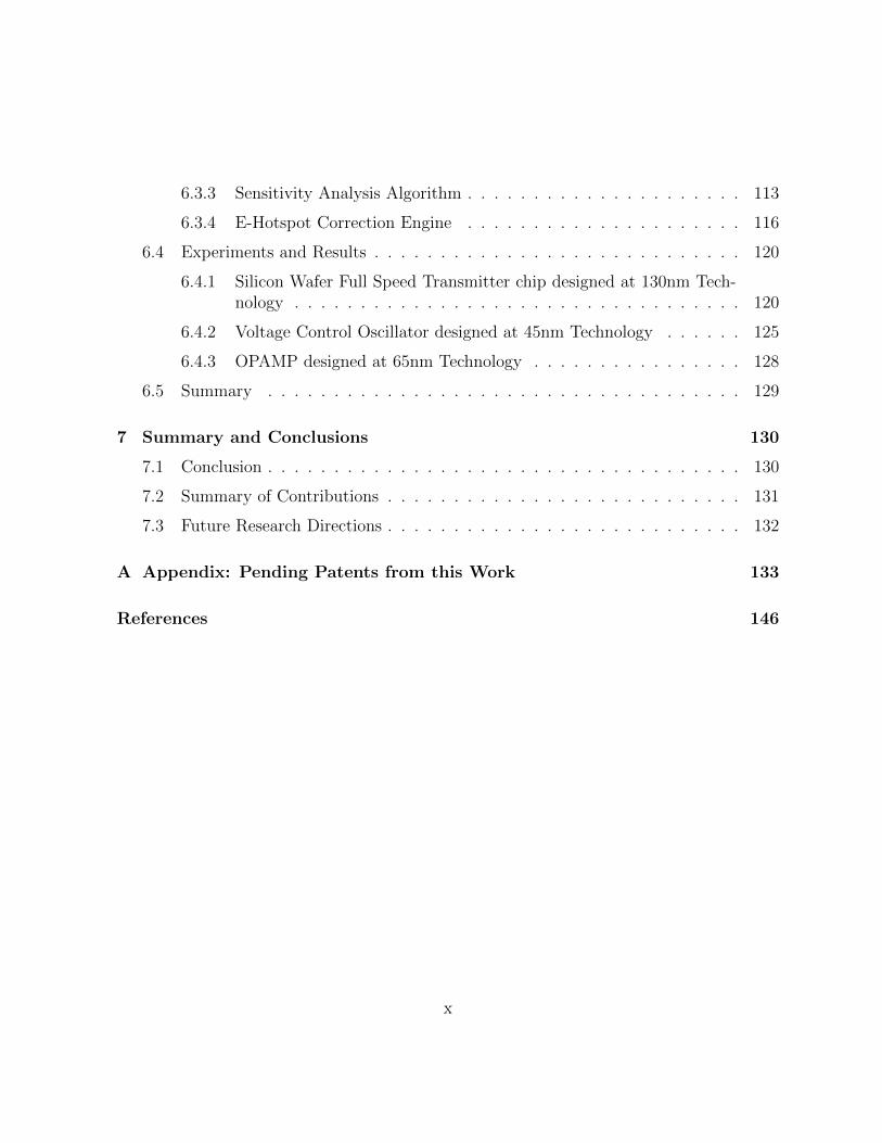
6.3.3 Sensitivity Analysis Algorithm . . . . . . . . . . . . . . . . . . . . . 113
6.3.4 E-Hotspot Correction Engine . . . . . . . . . . . . . . . . . . . . . 116
6.4 Experiments and Results . . . . . . . . . . . . . . . . . . . . . . . . . . . . 120
6.4.1 Silicon Wafer Full Speed Transmitter chip designed at 130nm Tech-nology . . . . . . . . . . . . . . . . . . . . . . . . . . . . . . . . . . 120
6.4.2 Voltage Control Oscillator designed at 45nm Technology . . . . . . 125
6.4.3 OPAMP designed at 65nm Technology . . . . . . . . . . . . . . . . 128
6.5 Summary . . . . . . . . . . . . . . . . . . . . . . . . . . . . . . . . . . . . 129
7 Summary and Conclusions 130
7.1 Conclusion . . . . . . . . . . . . . . . . . . . . . . . . . . . . . . . . . . . . 130
7.2 Summary of Contributions . . . . . . . . . . . . . . . . . . . . . . . . . . . 131
7.3 Future Research Directions . . . . . . . . . . . . . . . . . . . . . . . . . . . 132
A Appendix: Pending Patents from this Work 133
References 146
x

List of Tables
3.1 Example of the Electrical Simulation Results for NAND gate . . . . . . . . 52
4.1 DFM-properties for different Standard cells . . . . . . . . . . . . . . . . . 76
4.2 Timing reports simulating standard netlist versus process-aware netlists . 78
5.1 Grouping the devices as an output from the Device Parameter MatchingEngine- Group 1: contains 4 matched transistors . . . . . . . . . . . . . . . 98
5.2 Grouping the devices as an output from the Device Parameter MatchingEngine- Group 2: contains 8 matched transistors . . . . . . . . . . . . . . . 98
5.3 Top five device groups experiencing variation in the DC current values . . 98
5.4 Result comparison between previous hotspot detection methods and ourmethod . . . . . . . . . . . . . . . . . . . . . . . . . . . . . . . . . . . . . 100
xi

List of Figures
1.1 Defect categories by yield and process nodes [1] . . . . . . . . . . . . . . . 2
1.2 Systematic Variation Aware Analysis and Design Enhancement Techniques 5
2.1 Schematic of a step-and-scan wafer stepper. [2] . . . . . . . . . . . . . . . 11
2.2 Features on the mask cannot be exactly reconstructed due to diffraction. [2] 13
2.3 Equipment used for CMP. [3] . . . . . . . . . . . . . . . . . . . . . . . . . 15
2.4 Dishing and Erosion. [4] . . . . . . . . . . . . . . . . . . . . . . . . . . . . 15
2.5 A depiction of the STI stress effect.[5] . . . . . . . . . . . . . . . . . . . . . 16
2.6 A depiction of the WPE.[5] . . . . . . . . . . . . . . . . . . . . . . . . . . 17
2.7 The limits of lithography techniques and the changes in printed results acrossprocess nodes [6] . . . . . . . . . . . . . . . . . . . . . . . . . . . . . . . . 20
2.8 Measured Vth versus channel length L for a 90nm which shows strong shortchannel effects causing sharp roll-off for Vth for shorter L.[4] . . . . . . . . 21
2.9 Ion and Ioff variations due to transistor length [7] . . . . . . . . . . . . . . 22
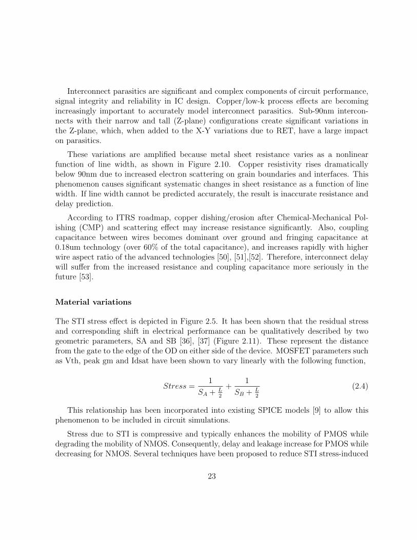
2.10 Interconnect resistance variation due to width. [8] . . . . . . . . . . . . . . 24
2.11 MOSFET device geometry using a shallow trench isolation scheme. [9] . . 24
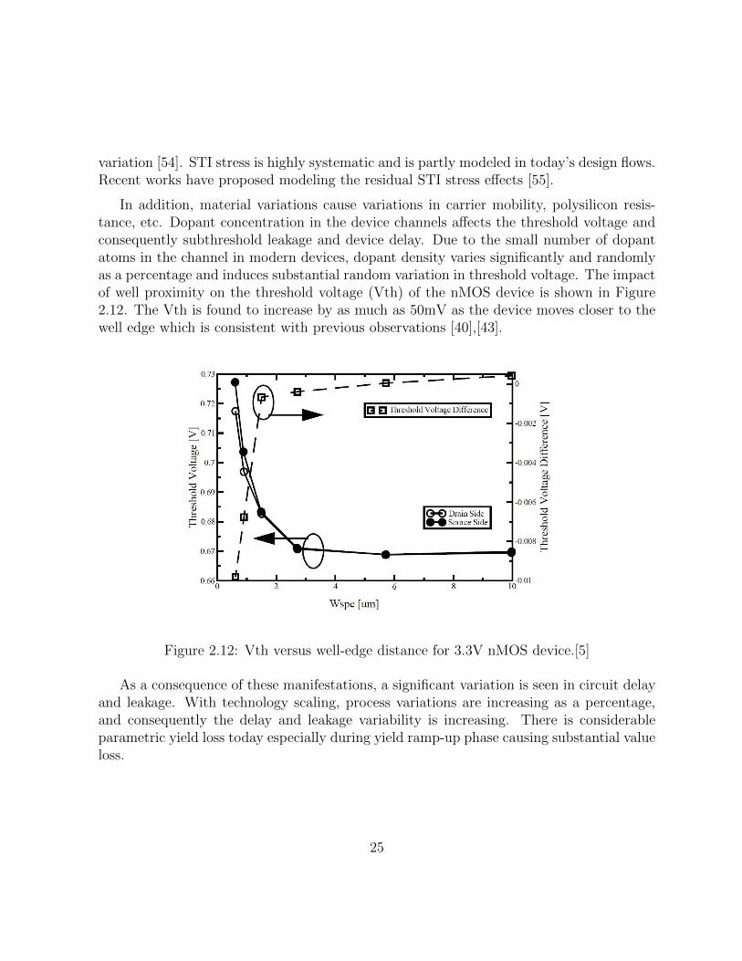
2.12 Vth versus well-edge distance for 3.3V nMOS device.[5] . . . . . . . . . . . 25
2.13 Systematic Variation Aware Analysis and Design Enhancement . . . . . . 30
2.14 Flow diagram of a lithography model [10] . . . . . . . . . . . . . . . . . . . 33
3.1 Experimental data for pitch curve with feature type classification. [11] . . . 42
3.2 Stress effect on Ion for simple layout implementations.[12] . . . . . . . . . 43
xii
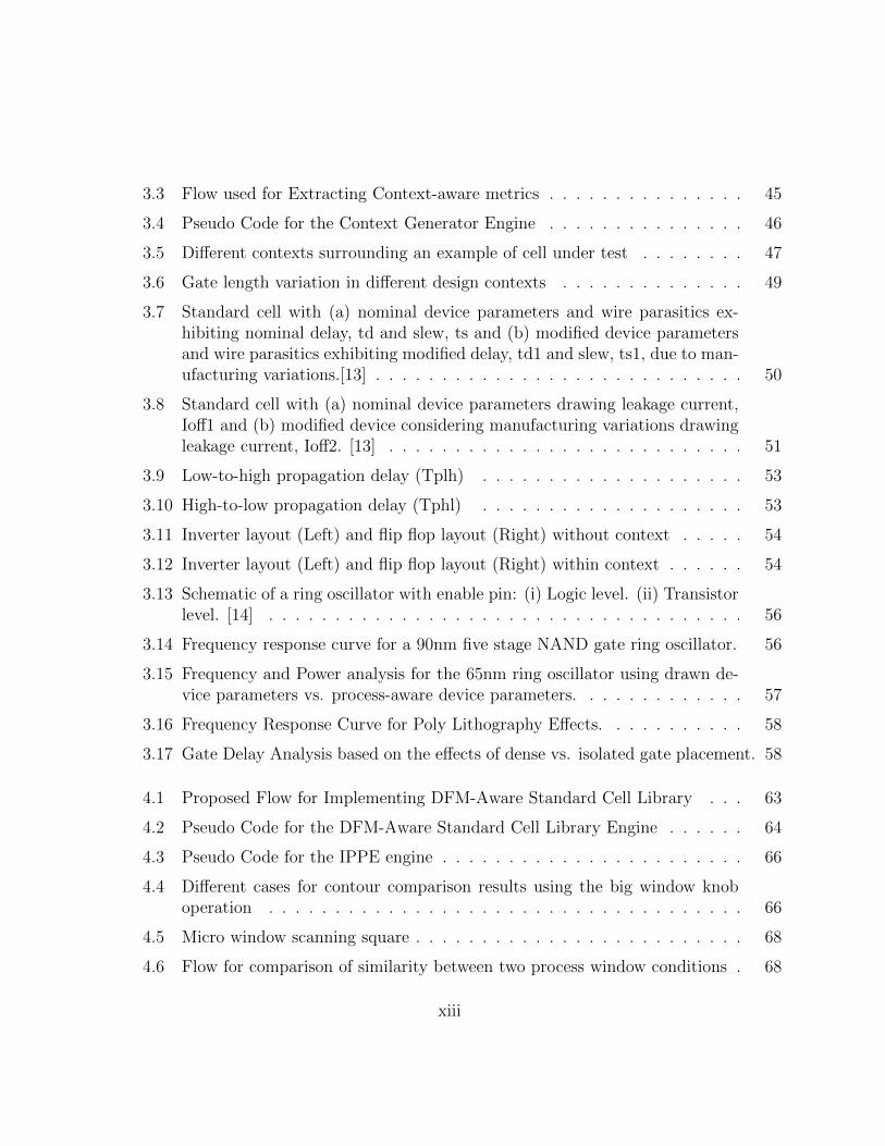
3.3 Flow used for Extracting Context-aware metrics . . . . . . . . . . . . . . . 45
3.4 Pseudo Code for the Context Generator Engine . . . . . . . . . . . . . . . 46
3.5 Different contexts surrounding an example of cell under test . . . . . . . . 47
3.6 Gate length variation in different design contexts . . . . . . . . . . . . . . 49
3.7 Standard cell with (a) nominal device parameters and wire parasitics ex-hibiting nominal delay, td and slew, ts and (b) modified device parametersand wire parasitics exhibiting modified delay, td1 and slew, ts1, due to man-ufacturing variations.[13] . . . . . . . . . . . . . . . . . . . . . . . . . . . . 50
3.8 Standard cell with (a) nominal device parameters drawing leakage current,Ioff1 and (b) modified device considering manufacturing variations drawingleakage current, Ioff2. [13] . . . . . . . . . . . . . . . . . . . . . . . . . . . 51
3.9 Low-to-high propagation delay (Tplh) . . . . . . . . . . . . . . . . . . . . 53
3.10 High-to-low propagation delay (Tphl) . . . . . . . . . . . . . . . . . . . . 53
3.11 Inverter layout (Left) and flip flop layout (Right) without context . . . . . 54
3.12 Inverter layout (Left) and flip flop layout (Right) within context . . . . . . 54
3.13 Schematic of a ring oscillator with enable pin: (i) Logic level. (ii) Transistorlevel. [14] . . . . . . . . . . . . . . . . . . . . . . . . . . . . . . . . . . . . 56
3.14 Frequency response curve for a 90nm five stage NAND gate ring oscillator. 56
3.15 Frequency and Power analysis for the 65nm ring oscillator using drawn de-vice parameters vs. process-aware device parameters. . . . . . . . . . . . . 57
3.16 Frequency Response Curve for Poly Lithography Effects. . . . . . . . . . . 58
3.17 Gate Delay Analysis based on the effects of dense vs. isolated gate placement. 58
4.1 Proposed Flow for Implementing DFM-Aware Standard Cell Library . . . 63
4.2 Pseudo Code for the DFM-Aware Standard Cell Library Engine . . . . . . 64
4.3 Pseudo Code for the IPPE engine . . . . . . . . . . . . . . . . . . . . . . . 66
4.4 Different cases for contour comparison results using the big window knoboperation . . . . . . . . . . . . . . . . . . . . . . . . . . . . . . . . . . . . 66
4.5 Micro window scanning square . . . . . . . . . . . . . . . . . . . . . . . . . 68
4.6 Flow for comparison of similarity between two process window conditions . 68
xiii
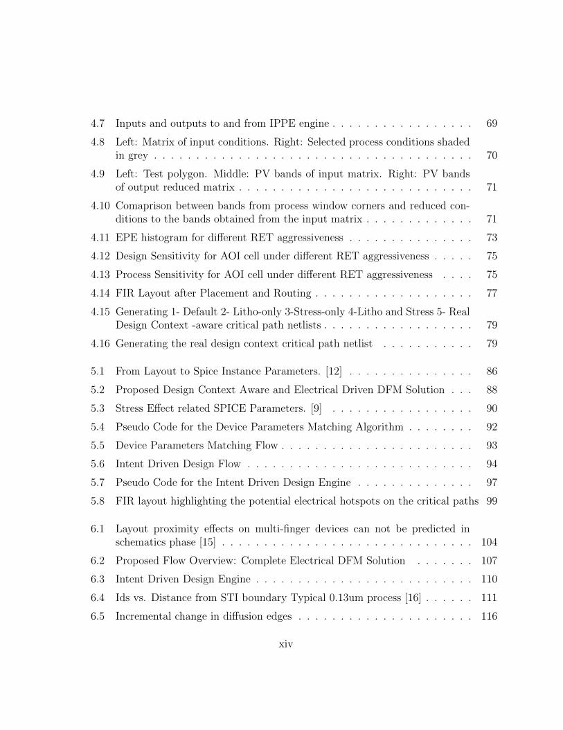
4.7 Inputs and outputs to and from IPPE engine . . . . . . . . . . . . . . . . . 69
4.8 Left: Matrix of input conditions. Right: Selected process conditions shadedin grey . . . . . . . . . . . . . . . . . . . . . . . . . . . . . . . . . . . . . . 70
4.9 Left: Test polygon. Middle: PV bands of input matrix. Right: PV bandsof output reduced matrix . . . . . . . . . . . . . . . . . . . . . . . . . . . . 71
4.10 Comaprison between bands from process window corners and reduced con-ditions to the bands obtained from the input matrix . . . . . . . . . . . . . 71
4.11 EPE histogram for different RET aggressiveness . . . . . . . . . . . . . . . 73
4.12 Design Sensitivity for AOI cell under different RET aggressiveness . . . . . 75
4.13 Process Sensitivity for AOI cell under different RET aggressiveness . . . . 75
4.14 FIR Layout after Placement and Routing . . . . . . . . . . . . . . . . . . . 77
4.15 Generating 1- Default 2- Litho-only 3-Stress-only 4-Litho and Stress 5- RealDesign Context -aware critical path netlists . . . . . . . . . . . . . . . . . . 79
4.16 Generating the real design context critical path netlist . . . . . . . . . . . 79
5.1 From Layout to Spice Instance Parameters. [12] . . . . . . . . . . . . . . . 86
5.2 Proposed Design Context Aware and Electrical Driven DFM Solution . . . 88
5.3 Stress Effect related SPICE Parameters. [9] . . . . . . . . . . . . . . . . . 90
5.4 Pseudo Code for the Device Parameters Matching Algorithm . . . . . . . . 92
5.5 Device Parameters Matching Flow . . . . . . . . . . . . . . . . . . . . . . . 93
5.6 Intent Driven Design Flow . . . . . . . . . . . . . . . . . . . . . . . . . . . 94
5.7 Pseudo Code for the Intent Driven Design Engine . . . . . . . . . . . . . . 97
5.8 FIR layout highlighting the potential electrical hotspots on the critical paths 99
6.1 Layout proximity effects on multi-finger devices can not be predicted inschematics phase [15] . . . . . . . . . . . . . . . . . . . . . . . . . . . . . . 104
6.2 Proposed Flow Overview: Complete Electrical DFM Solution . . . . . . . 107
6.3 Intent Driven Design Engine . . . . . . . . . . . . . . . . . . . . . . . . . . 110
6.4 Ids vs. Distance from STI boundary Typical 0.13um process [16] . . . . . . 111
6.5 Incremental change in diffusion edges . . . . . . . . . . . . . . . . . . . . . 116
xiv
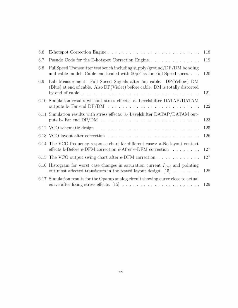
6.6 E-hotspot Correction Engine . . . . . . . . . . . . . . . . . . . . . . . . . . 118
6.7 Pseudo Code for the E-hotspot Correction Engine . . . . . . . . . . . . . . 119
6.8 FullSpeed Transmitter testbench including supply/ground/DP/DM bondingand cable model. Cable end loaded with 50pF as for Full Speed specs. . . . 120
6.9 Lab Measurement: Full Speed Signals after 5m cable. DP(Yellow) DM(Blue) at end of cable. Also DP(Violet) before cable. DM is totally distortedby end of cable. . . . . . . . . . . . . . . . . . . . . . . . . . . . . . . . . . 121
6.10 Simulation results without stress effects: a- Levelshifter DATAP/DATAMoutputs b- Far end DP/DM . . . . . . . . . . . . . . . . . . . . . . . . . . 122
6.11 Simulation results with stress effects: a- Levelshifter DATAP/DATAM out-puts b- Far end DP/DM . . . . . . . . . . . . . . . . . . . . . . . . . . . . 123
6.12 VCO schematic design . . . . . . . . . . . . . . . . . . . . . . . . . . . . . 125
6.13 VCO layout after correction . . . . . . . . . . . . . . . . . . . . . . . . . . 126
6.14 The VCO frequency response chart for different cases: a-No layout contexteffects b-Before e-DFM correction c-After e-DFM correction . . . . . . . . 127
6.15 The VCO output swing chart after e-DFM correction . . . . . . . . . . . . 127
6.16 Histogram for worst case changes in saturation current Idsat and pointingout most affected transistors in the tested layout design. [15] . . . . . . . . 128
6.17 Simulation results for the Opamp analog circuit showing curve close to actualcurve after fixing stress effects. [15] . . . . . . . . . . . . . . . . . . . . . . 129
xv

Chapter 1
Introduction and Motivation
1.1 Introduction
CMOS device scaling has outpaced advancements in manufacturing technologies. Thus,process variability compared to the feature size, continues to increase. Many designers havestarted to recognize that this push into advanced nodes has exposed a hitherto insignificantset of yield problems [1] [17]. Physical yield problems are known to cause catastrophicfailures, such as bridging faults, have always been the primary focus of verification efforts.At sub-90nm technologies, integrated circuit (IC) designs are also exhibiting parametricyield failures [18]. Parametric yield issues arise when the process variations have not beensufficiently characterized such that a circuit might have achieved design closure throughstandard methodologies, but the silicon performance does not match the simulation results.
At sub-90nm technologies, yields drastically drop-off, as designs fail to consistentlyachieve their technical and competitive objectives [19]. As more and more features areplaced into smaller and smaller spaces, the unintended effects of this crowding are creat-ing havoc with yield and performance. Designers need to be aware that device behaviordepends not only on traditional geometric parameters such as channel length and width,but also on layout implementation details of the device and its surrounding neighborhood.Figure 1.1 illustrates that within the category of systematic yield defects, there are twosubcategories: 1- lithography/new materials-based and 2- design-based [1]. At the 130 nmnode, the systematic defects are roughly, an equal split between the two subcategories. Adramatic increase of defects is obvious at the 90nm node, where the ratio is approximately2.5:1 for design-based versus lithography/new materials yield defects [20].
1
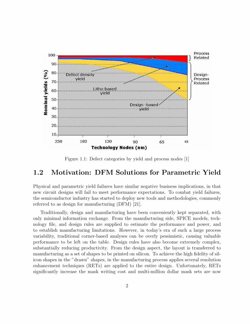
Figure 1.1: Defect categories by yield and process nodes [1]
1.2 Motivation: DFM Solutions for Parametric Yield
Physical and parametric yield failures have similar negative business implications, in thatnew circuit designs will fail to meet performance expectations. To combat yield failures,the semiconductor industry has started to deploy new tools and methodologies, commonlyreferred to as design for manufacturing (DFM) [21].
Traditionally, design and manufacturing have been conveniently kept separated, withonly minimal information exchange. From the manufacturing side, SPICE models, tech-nology file, and design rules are supplied to estimate the performance and power, andto establish manufacturing limitations. However, in today’s era of such a large processvariability, traditional corner-based analyses can be overly pessimistic, causing valuableperformance to be left on the table. Design rules have also become extremely complex,substantially reducing productivity. From the design aspect, the layout is transferred tomanufacturing as a set of shapes to be printed on silicon. To achieve the high fidelity of sil-icon shapes in the ”drawn” shapes, in the manufacturing process applies several resolutionenhancement techniques (RETs) are applied to the entire design. Unfortunately, RETssignificantly increase the mask writing cost and multi-million dollar mask sets are now
2

common. To reduce the mask cost, it is crucial to additionally convey the design intentto manufacturing so that high fidelity is attempted only for selected features in the designthat require accurate manufacturing. DFM techniques essentially address the questionsrelated to the exchange of information across design and manufacturing, and the use ofthis information for yield enhancement.
Most efforts have been concentrated on catastrophic failures, or physical DFM prob-lems. Recently, there has been an increased emphasis on parametric yield issues. A com-prehensive DFM methodology reduces the parametric yield loss and leads to maximizedutilization of the process. More sophisticated parametric-based DFM solutions are theones that can perform different tasks:
• Predict: Designers can improve the parametric yield and chip performance by ac-curately determining the impact of systematic variations during the design stages.
• Analyze: Designers can quickly analyze various types of manufacturing non-idealities.
• Enhance: Designers can reduce sensitivity to manufacturing variations to achievethe desired predictability.
The goal of this thesis is on developing parametric-based DFM computer-aided design(CAD) tools for systematic variation analysis and design enhancement techniques.
1.3 Thesis Outline
In the next chapter, the relevant literature is reviewed to demonstrate the need to proposenew ways to augment the yield.
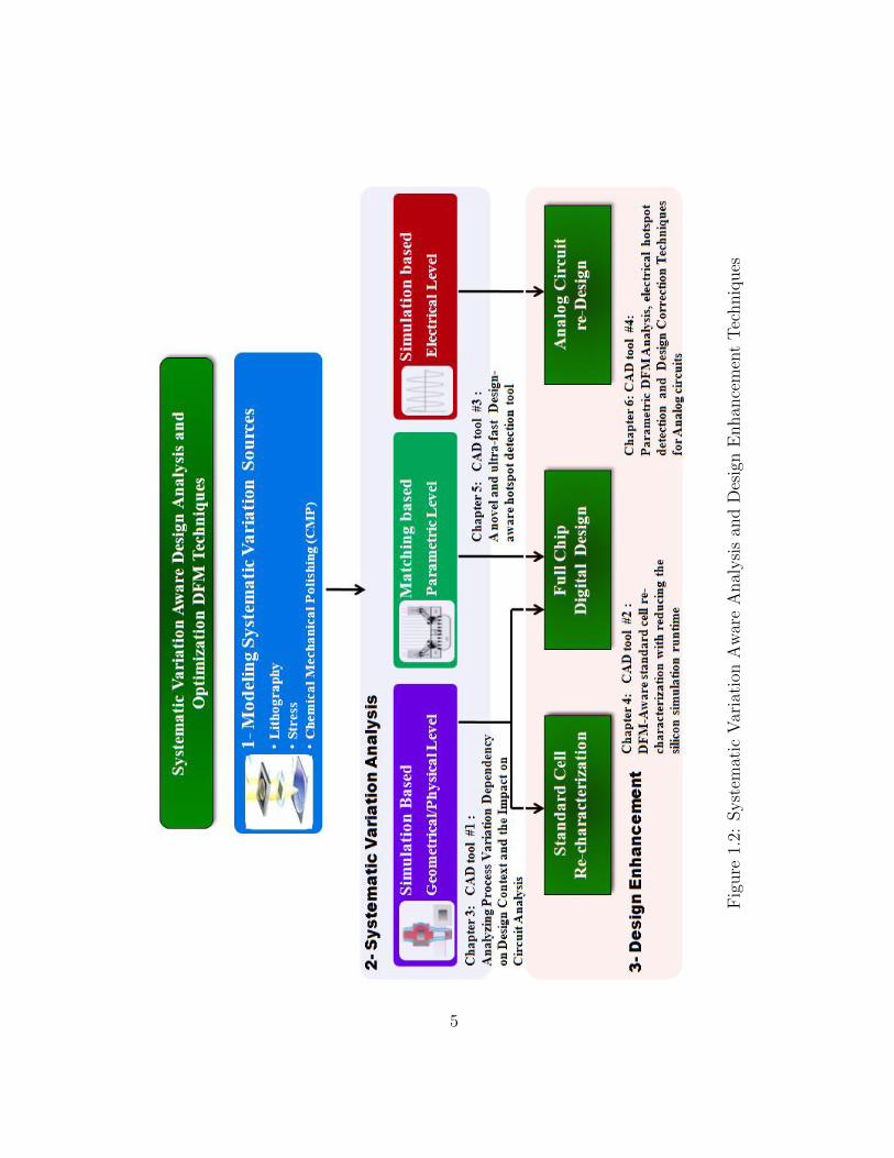
Four CAD tools are proposed and developed in this thesis, as denoted in Figure 1.2.The first CAD tool, presented in Chapter 3, to facilitate a quantitative analysis of thesystematic variation impact on different circuits in terms of electrical and geometricalbehavior. Extensive lithography and stress analysis is performed under different designcontext.
In Chapter 4, a second CAD tool is proposed to manifest the ”fix before design philos-ophy”, avoiding long design cycles and re-spins. This is implemented by re-characterizingthe standard cell library comprising different design context, different resolution enhance-ment techniques and different process conditions using a newly developed methodology that
3
dramatically reduces the required number of silicon simulations. Experiments prove thatthe DFM-aware standard cell library results in more robust and manufacturable designs.
Chapter 5 presents a novel electrical-aware hotspot detection solution by using a de-vice parameter-based matching technique. While the state-of-the-art hotspot detectionsolutions are all geometrical based, this hotspot detection methodology experimentallydemonstrates extraordinary fast and accurate results.
The existing DFM solutions that are focused on analyzing and detecting the electricalvariations, principally address digital designs. On the other hand, process variations playan increasingly important role in the success of analog circuits. The fourth CAD solution,proposed in this thesis and presented in Chapter 6, introduces a variability-aware DFMsolution that detects and automatically corrects hotspots for analog circuits.
Finally the contributions, conclusion and suggestions for future work are summarizedin Chapter 7.
1.4 Thesis Contributions
• Implement four CAD solutions that tackle parametric and physical yield issues.These solutions enable the designers to achieve faster and accurate systematic varia-tion analyses. In addition, designers are provided with different design enhancementand correction techniques.
• Novel CAD engines are introduced to solve key challenges that present state-of-the-artDFM solutions can not achieve. For example, systematic variation analysis flows forfull chip digital designs face several challenges, mainly the high computational siliconsimulation time. To address this issue, a novel solution is introduced to highly reducethe lithography simulation runtime (nearly 90%) compared to running lithographysimulation using the complete set of different process conditions, with a minimumimpact on accuracy. Another proposed engine uses SPICE parameter matching tech-niques for hotspot detection, avoid the need for silicon simulations and can identifythe hotspots in matter of seconds. Another challenge with the current DFM solutionsis the lack of design awareness. Most, if not all, hotspot detection solutions generatethousands of hotspots which challenges designers as to which hotspots are criticalfrom the design point of view. Therefore a design intent driven engine that addsdesign awareness to the hotspot detection engines is introduced. It is worth mention-ing that this engine is currently implemented within industrial CAD tools: Calibre
4
Fig
ure
1.2:
Syst
emat
icV
aria
tion
Aw
are
Anal
ysi
san
dD
esig
nE
nhan
cem
ent
Tec
hniq
ues
5

PERC LDL Mentor Graphics, and tested in the industry at ON-SemiconductorCorp. design team.
• New philosophies are adopted in these newly designed DFM CAD solutions. Forexample, the current DFM solutions are mostly geometrical-based where a processvariation analysis is run on the physical layout level. Also introduced is an electricaldriven hotspot detection solution that stems from a SPICE parameter matchingtechnique. Beside that solution, there is another CAD solution that supports the”fixing before design” philosophy which provides a more robust and manufacture-able physical layout designs that will reduce design re-spins and also reduce thenumber of hotspots.
• The proposed CAD solutions target different design types. One of the proposed CADsolutions is considered one of the first complete DFM solutions (Detection-Analysis-Correction), which is dedicated to solve parametric yield issues for analog circuits.
• These CAD solutions are technology independent and tested on industrial testcasesdesigned in 65nm and 45nm technologies. Silicon-tested circuits are also used toverify these solutions.
6

Chapter 2
Background: Process Variations andDFM Solutions
2.1 Introduction
Process variation has long been a concern in integrated circuit design, manufacture, andoperation. In recent years, with continued scaling and demand for higher performance andhigher yield, the need and interest in techniques and tools that address variation has in-creased. The impact of process variations on circuit power and performance is exacerbatedby the superlinear dependence of several electrical metrics on feature size (e.g., subthresh-old leakage on gate length, and gate tunneling leakage on gate oxide thickness) [22]. Power,and especially leakage power, is another major challenge faced by designers today. Lower-ing of supply voltage to reduce dynamic power necessitates lowering of threshold voltage tosustain high-performance and adequate noise margins. Unfortunately, lowering thresholdvoltage causes a near-exponential increase in leakage power, and a larger ratio of static(”wasted”) power to total power. Leakage variability, which is increasingly a determinantof parametric yield, is another important problem that must be addressed for continuedCMOS scaling.
Traditionally, design and manufacturing have been conveniently kept separated, withonly minimal information exchange. From the manufacturing side, SPICE models, tech-nology file, and design rules are supplied for performance and power estimation, and toconvey manufacturing limitations. However, in today’s era of large process variability, tra-ditional corner-based analyses can be overly pessimistic, causing valuable performance tobe left on the table. Design rules also become extremely complex, substantially reducing
7
productivity. From the design side, the layout is transferred to manufacturing as a setof shapes to be printed on silicon. To achieve high fidelity of silicon shapes to ”drawn”shapes, the manufacturing side applies several resolution enhancement techniques (RETs)to the entire design. Unfortunately, RETs significantly increase the mask writing cost andmulti-million dollar mask sets are now common. To reduce mask cost, it is important toadditionally convey the design intent to manufacturing so that high fidelity is attemptedonly for selected features in the design that require accurate manufacturing. Design formanufacturing (DFM) techniques essentially address the questions related to the exchangeof information across design and manufacturing, and the use of this information for yieldenhancement.
To better understand DFM, we first present a brief overview of major sources of processvariations.
2.2 Sources of Process Variations
Variation is the deviation from intended values for structure or a parameter of concern[4]. The electrical performance of modern IC is subject to different sources of variationsthat affect both the device (transistor) and the interconnects. For the purposes of circuitdesign, the sources of variation can broadly be categorized into two classes [23], [24], [25]:
1. Inter-Die variations: also called global variations, are variations from die to die, waferto wafer, and lot to lot. These variations affect all devices on the same chip in thesame way (e.g., they may cause all the transistors’ gate lengths’ to be larger than anominal value).
2. Within-Die (WID): also called local or intra-die variations, correspond to variabilitywithin a single chip, and may affect different devices differently on the same chip.In nanoscale regime, dimensions are small enough that device behavior is largelydependent of the neighborhood of the device. (e.g., some devices on the same diemay have larger channel length L than the rest of the devices).
Inter-Die variations have been a longstanding design issue, and are typically dealt withusing corner models [23]. These corners are chosen to account for the circuit behavior underworst-case variation and were considered efficient in older technologies where the majorsources of variation were inter-die variations. However, in nanometer technologies, WIDvariations have become significant and can no longer be ignored [26], [27], [28]. As a result,
8

process corners based design methodologies, where verification is performed at a smallnumber of design corners, are currently insufficient. WID variations can be subdividedinto two classes [23], [24], [25]:
• Random variations: As the name implies, are sources that show random behavior,and can be characterized using their statistical distribution. Random variations areinherent fluctuations in process parameters, such as random dopant fluctuations fromdie-to-die, wafer-to-wafer and lot-to-lot.
• Systematic variations: These types of variations depend on the layout pattern andare therefore predictable. Systematic variations are highly dependent on the physicallayout context (i.e. the systematic variations are dependent on the design). Exam-ples of systematic variations are topography variations due to Chemical MechanicalPolishing (CMP) dishing, linewidth variation due to lithography defocus and expo-sure, and stress due to shallow trench isolation (STI). These effects have a substantialbut deterministic impact on the critical dimension (CD) of a transistor gate or thewidth and thickness of an interconnect wire.
Historically, global random variations have been higher up the agenda than local sys-tematic variations. But below 90 nm, local systematic variations have become the foremostconcern [2]. The primary sources of manufacturing systematic variation will be discussedin more details.
2.2.1 Sources of Systematic Variations: Optical Lithography
Optical lithography, or simply lithography, is the mainstream technique to create patternson silicon wafers. While conceptually simple, lithography has evolved into a highly so-phisticated process due to precision requirements that are unmatched anywhere in modernmanufacturing. Lithography involves several steps which can be simplistically groupedinto photoresist deposition, exposure, and etching. The process begins with deposition ofa thin layer that is intended to be patterned on the wafer. The thin layer is sacrificial andis used to selectively etch, dope, oxidize or deposit the underlying material. The patternon the mask is first transferred to the photoresist that is deposited over the thin layer.An etchant is then used to remove the thin layer from where it is not protected by thephotoresist. We now briefly describe the major lithography steps, further details of whichcan be found in [29].
9
Photoresist and its Deposition
Photoresists are materials that when exposed to light undergo a photochemical reactionthat changes their solubility properties to a developer chemical. Positive photoresistsbecome soluble in the regions that are exposed to light while negative photoresists becomesoluble in the regions occluded from light. Prior to deposition of the photoresist, the wafermay optionally be treated with a chemical that promotes adhesion between the thin layerand the photoresist.
The standard method of depositing the photoresist onto the wafer is resist spinning. Inthis method, a small amount of the photoresist in liquid form is dispensed onto the centerof the wafer, and the wafer is then rotated about its center at a high rate. As the waferspins, the resist spreads radially and solidifies into a uniform solid layer over the wafer. Abaking step, known as soft bake, in which the wafer is heated to relatively low temperaturefor a short period of time, is then optionally performed to further densify the photoresist.Another optional step of coating the wafer with an anti-reflective coating (ARC) is thenperformed to suppress the light reflections in the succeeding exposure steps.
Exposure
By selectively exposing the photoresist to light, a pattern can be transferred to the pho-toresist. This process is accomplished in lithography by imaging of the mask to transferpatterns on it to the photoresist. The mask is a thin piece of a high-quality transparentmaterial, typically quartz, partially covered with an opaque material, typically chromium,that has been removed according to the circuit pattern using an electron-beam mask writer.
Over the years, mask writing technology has improved but has failed to keep pacewith the shrinkage of feature sizes. Thus, projection printing, in which projection optics(sometimes simply known as the lens) are used to reduce the mask image by a reductionfactor (N), is now mainstream. The projection optics are typically an array of high-quality lenses cascaded to realize the reduction factor with minimal image distortion. Thereduction factor in modern optics is most commonly equal to four or five. Larger reductionfactors relax the precision requirements on the mask and reduce the linewidth variationsdue to mask errors. However, larger reduction factors increase the size of the mask anddecrease the throughput in terms of the wafer area exposed under the mask. We note thatthe mask is also referred to as the reticle in the exposure context.
The equipment used to expose the photoresist-coated wafer is known as a wafer stepper.In a wafer stepper, a small portion of the wafer, known as the exposure field or simply the
10
field, is exposed under the reticle through the projection optics. The illumination is thenturned off and the wafer is displaced so that a different portion of the wafer is exposed inthe next step. Modern wafer steppers are extremely sophisticated, with very high steppingprecision. Additionally, steppers also align the wafer to the proper position so that theprojected image will precisely overlay the patterns already on the wafer from previouslithography steps.
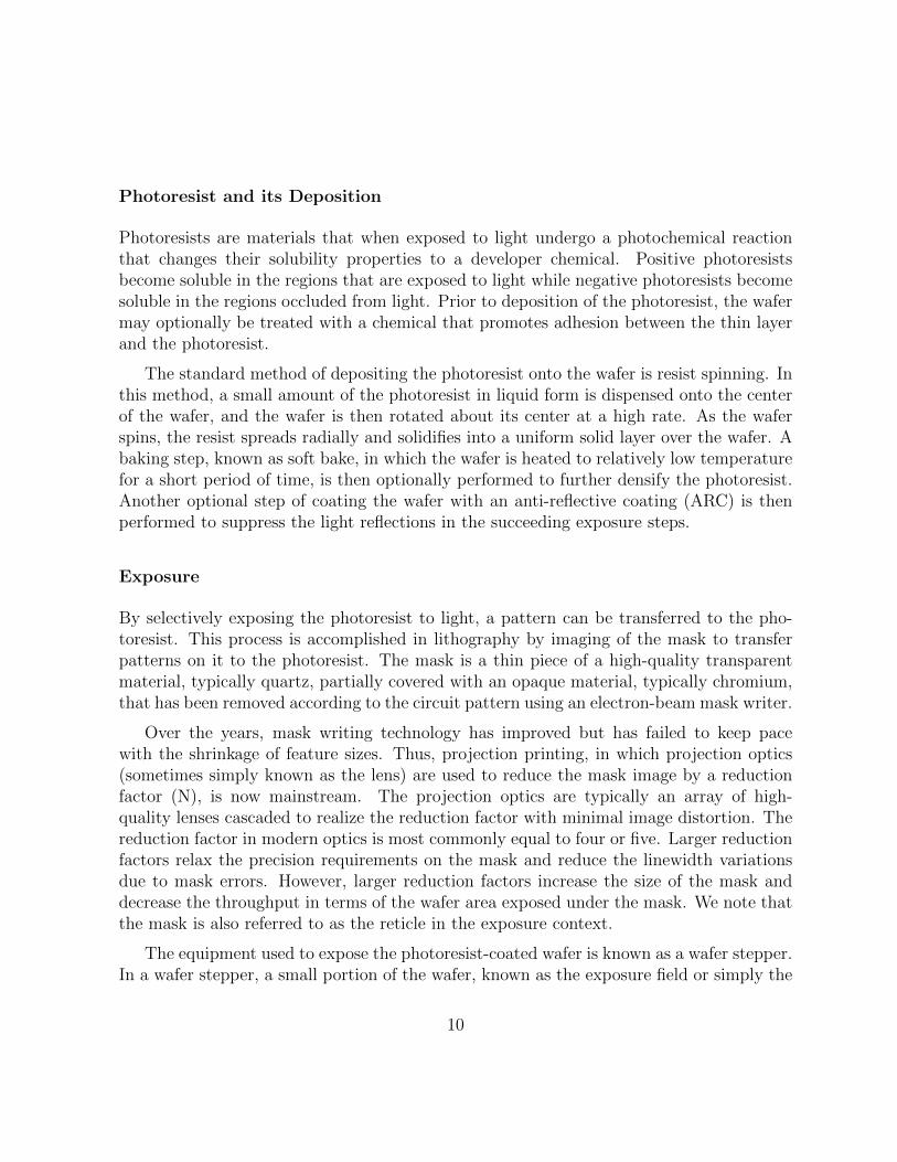
Modern wafer steppers are of the step-and-scan type in which the field is partiallyexposed through a slit [29], [30]. The lens and the wafer are translated synchronouslysuch that the illumination through the slit scans the field from side to side. Due to theimage reduction by the projection optics, the lens must be translated N (i.e., the reductionfactor) times faster than the wafer. Illumination through a small slit restricts the area ofthe projection optics that is utilized, which simplifies the projection optics and reducestheir distortions. A schematic of the step-and-scan system is shown in Figure 2.1.
Figure 2.1: Schematic of a step-and-scan wafer stepper. [2]
After the patterning process completes, the photoresist undergoes post-exposure bake,which entails heating at a higher temperature than soft bake. The purpose of post-exposurebake is to further drive off low molecular-weight materials that may contaminate the post-lithographic equipment. Post-exposure bake also smoothes out the resist line profiles.
11

Then, a developer solution washes away the soluble parts of the resist and the pattern hasbeen transferred from the mask to the photoresist.
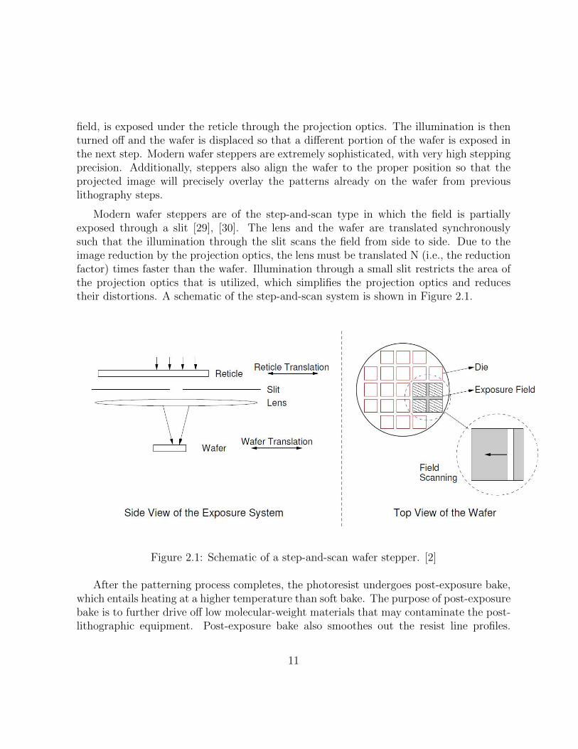
While the patterning process is highly sophisticated, the image on the mask undergoessignificant distortion as it is transferred to the photoresist. Due to the extremely smallsizes of the mask features, diffraction effects, inherent to the wave nature of light, becomeconsiderable. Unfortunately, a finite-sized lens is not capable of collecting all the diffractionorders as shown in Figure 2.2, and the mask image cannot be completely reconstructed.This fundamentally limits the resolving capability of lithography, which is given by thefollowing well-known Raleigh’s equation:
Lmin = k1 ∗ λ
NA(2.1)
• Lmin is the minimum feature size that can be resolved.
• λ is the wavelength of the illumination source. An ArF plasma source with a wave-length of 193nm is used in modern lithography, and is projected to remain in use atleast through the 45nm node.
• NA is the numerical aperture of the lens and is the sine of the maximum half-angleof light that can make it through a lens to the wafer, multiplied by the index ofrefraction of the medium (1.0 for air). The NA of a lens is a measure of its ability tocapture the diffraction orders of light across a wide range of incidence angles.
• k1 is known as the k-factor and captures the capability of the lithography process; ithas a fundamental lower limit of 0.25. For modern processes, k1 is around 0.3.
In addition to the minimum resolvable size, the depth of focus (DOF) is an importantparameter of a patterning system. Ideally, the wafer should be placed at the focal planeof the lens. This, in practice, is infeasible and the wafer, or certain parts of it, may bepositioned at a small distance, known as the defocus, from the focal plane. DOF capturesthe tolerance of a exposure system to defocus. DOF is given by
DOF = k2 ∗ λ
(NA)2(2.2)
where k2 is a constant. Similar to DOF, exposure latitude quantifies the toleranceto exposure dose variations. Together with DOF, exposure latitude gives the lithographyprocess window.
12
Figure 2.2: Features on the mask cannot be exactly reconstructed due to diffraction. [2]
Improvements in lithography equipment and resist technology, along with resolutionenhancement techniques (RETs), reduce the k-factor and consequently the minimum re-solvable size. RETs are methods used in lithography to enhance the printability of maskfeatures. RETs are typically applied after signoff and before or during the mask datapreparation stage. Commonly used RETs are as follows.
• Optical proximity correction (OPC) selectively alters the shapes of the mask patternsto compensate for patterning imperfections. OPC can be rule-based, which uses rulesdefined for different layout configurations, or model-based, which uses a lithographysimulator. While OPC is very effective at reducing patterning variation, it requiresa large runtime and significantly increases the mask complexity.
• Off-axis illumination (OAI) refers to illumination which has no on-axis component,i.e., which has no light that is normally incident on the mask. Examples of off-axisillumination include annular and quadrupole illumination. OAI improves the DOFfor certain pitches while worsening it for others that are known as forbidden pitches.Fortunately, sub-resolution assist features can be inserted to eliminate or reduce theimpact of the forbidden pitches.
13
• Sub-resolution assist features (SRAFs) or scattering bars are layout features thatare inserted between layout features to improve their printability. SRAFs have verynarrow widths and do not print on the wafer.
• Phase shift mask (PSM) adds transparent layers to the mask in certain locations toinduce destructive interference at feature edges, which enhances pattern contrast andimproves the k-factor.
Etching
Etching is used to transfer the pattern from the photoresist to the underlying thin layer.The chemical used in etching is known as the etchant; it selectively reacts with the underly-ing thin layer only in the areas that are not protected by the photoresist, while leaving thephotoresist intact. The most common etching technique is reactive ion etching in whichchemically reactive plasma is used to remove the thin layer in regions not protected byphotoresist. After etching, the photoresist is completely removed by a variety of methods(e.g., dry etching [31]).
2.2.2 Sources of Systematic Variations: Chemical MechanicalPolishing
Chemical Mechanical Polishing (CMP) is the mainstream planarization technique used toremove excess deposited material and to attain wafer planarity over short and long ranges[32]. CMP involves use of chemicals to soften the material to be removed, and mechanicalabrasion to polish away the material. Rotary CMP tools are the most prevalent andprimarily consist of a rotating carrier on which the wafer is mounted, and a large polishingpad that rotates in the same direction. The wafer is held face down and pressed againstthe pad. To assist polishing, slurry, which is a mixture of abrasive particles and chemicalsthat soften the material to be polished, is fed onto the pad. CMP continues until thedesired thickness is attained. A common method for endpoint detection (i.e., when to stoppolishing), is the use of etch-stop materials which cause the motors to draw detectably morecurrent when the desired thickness is attained. The basic setup of rotary CMP equipmentis illustrated in Figure 2.3. CMP is used to planarize bare wafers, in front-end-of-line(FEOL) to remove and planarize overburden oxide, and in back-end-of-line (BEOL) toremove excess copper and barrier, and to planarize inter-level dielectric.
While several advancements have been made in CMP technology, imperfections remainand have always been a concern due to rapidly shrinking topography variation tolerances.
14
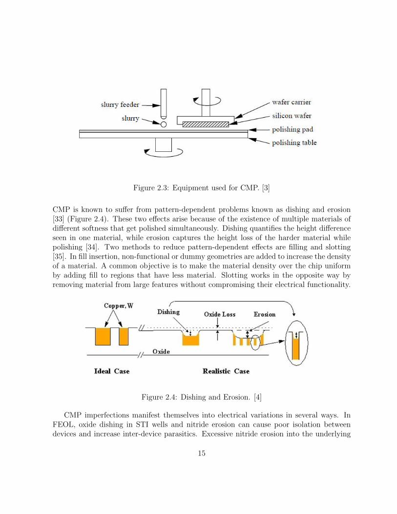
Figure 2.3: Equipment used for CMP. [3]
CMP is known to suffer from pattern-dependent problems known as dishing and erosion[33] (Figure 2.4). These two effects arise because of the existence of multiple materials ofdifferent softness that get polished simultaneously. Dishing quantifies the height differenceseen in one material, while erosion captures the height loss of the harder material whilepolishing [34]. Two methods to reduce pattern-dependent effects are filling and slotting[35]. In fill insertion, non-functional or dummy geometries are added to increase the densityof a material. A common objective is to make the material density over the chip uniformby adding fill to regions that have less material. Slotting works in the opposite way byremoving material from large features without compromising their electrical functionality.
Figure 2.4: Dishing and Erosion. [4]
CMP imperfections manifest themselves into electrical variations in several ways. InFEOL, oxide dishing in STI wells and nitride erosion can cause poor isolation betweendevices and increase inter-device parasitics. Excessive nitride erosion into the underlying
15
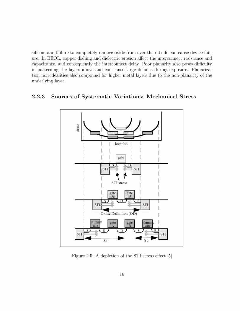
silicon, and failure to completely remove oxide from over the nitride can cause device fail-ure. In BEOL, copper dishing and dielectric erosion affect the interconnect resistance andcapacitance, and consequently the interconnect delay. Poor planarity also poses difficultyin patterning the layers above and can cause large defocus during exposure. Planariza-tion non-idealities also compound for higher metal layers due to the non-planarity of theunderlying layer.
2.2.3 Sources of Systematic Variations: Mechanical Stress
Figure 2.5: A depiction of the STI stress effect.[5]
16
For sub-0.25um CMOS technologies, the most prevalent isolation scheme is shallowtrench isolation (STI). Mechanical stress on active regions of devices arising due to theproximity and width of STI wells are significant in existing technologies. The STI processleaves behind a silicon island that is in a non-uniform state of bi-axial compressive stress [5],[36], [37]. STI induced stress has been shown to have an impact on device performance [38],[36],[39],[37],[40],[41], introducing both Idsat and Vth offsets. These effects are significantand must be included when modeling the performance of a transistor. The stress statewithin an active opening is both non-uniform and dependent on the overall size of theactive opening, meaning that MOSFET characteristics are once again a strong function oflayout. The STI stress effect is depicted in Figure 2.5
2.2.4 Sources of Systematic Variations: Material Dopping
Figure 2.6: A depiction of the WPE.[5]
Highly scaled bulk CMOS technologies make use of high energy implants to form thedeep retrograde well profiles needed for latch-up protection and suppression of lateral
17
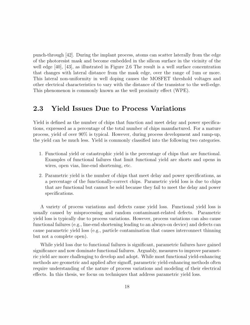
punch-through [42]. During the implant process, atoms can scatter laterally from the edgeof the photoresist mask and become embedded in the silicon surface in the vicinity of thewell edge [40], [43], as illustrated in Figure 2.6 The result is a well surface concentrationthat changes with lateral distance from the mask edge, over the range of 1um or more.This lateral non-uniformity in well doping causes the MOSFET threshold voltages andother electrical characteristics to vary with the distance of the transistor to the well-edge.This phenomenon is commonly known as the well proximity effect (WPE).
2.3 Yield Issues Due to Process Variations
Yield is defined as the number of chips that function and meet delay and power specifica-tions, expressed as a percentage of the total number of chips manufactured. For a matureprocess, yield of over 90% is typical. However, during process development and ramp-up,the yield can be much less. Yield is commonly classified into the following two categories.
1. Functional yield or catastrophic yield is the percentage of chips that are functional.Examples of functional failures that limit functional yield are shorts and opens inwires, open vias, line-end shortening, etc.
2. Parametric yield is the number of chips that meet delay and power specifications, asa percentage of the functionally-correct chips. Parametric yield loss is due to chipsthat are functional but cannot be sold because they fail to meet the delay and powerspecifications.
A variety of process variations and defects cause yield loss. Functional yield loss isusually caused by misprocessing and random contaminant-related defects. Parametricyield loss is typically due to process variations. However, process variations can also causefunctional failures (e.g., line-end shortening leading to an always-on device) and defects cancause parametric yield loss (e.g., particle contamination that causes interconnect thinningbut not a complete open).
While yield loss due to functional failures is significant, parametric failures have gainedsignificance and now dominate functional failures. Arguably, measures to improve paramet-ric yield are more challenging to develop and adopt. While most functional yield-enhancingmethods are geometric and applied after signoff, parametric yield-enhancing methods oftenrequire understanding of the nature of process variations and modeling of their electricaleffects. In this thesis, we focus on techniques that address parametric yield loss.
18
2.3.1 Impact of Process Variations on Parametric yield
Process variations, which are the primary cause of parametric yield loss, manifest them-selves as circuit metric (power and delay) variations in the following ways.
Lateral dimension variations
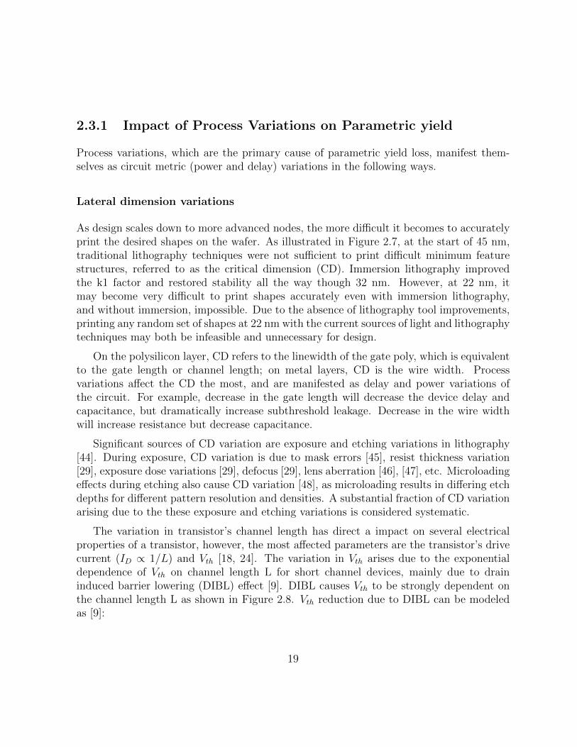
As design scales down to more advanced nodes, the more difficult it becomes to accuratelyprint the desired shapes on the wafer. As illustrated in Figure 2.7, at the start of 45 nm,traditional lithography techniques were not sufficient to print difficult minimum featurestructures, referred to as the critical dimension (CD). Immersion lithography improvedthe k1 factor and restored stability all the way though 32 nm. However, at 22 nm, itmay become very difficult to print shapes accurately even with immersion lithography,and without immersion, impossible. Due to the absence of lithography tool improvements,printing any random set of shapes at 22 nm with the current sources of light and lithographytechniques may both be infeasible and unnecessary for design.
On the polysilicon layer, CD refers to the linewidth of the gate poly, which is equivalentto the gate length or channel length; on metal layers, CD is the wire width. Processvariations affect the CD the most, and are manifested as delay and power variations ofthe circuit. For example, decrease in the gate length will decrease the device delay andcapacitance, but dramatically increase subthreshold leakage. Decrease in the wire widthwill increase resistance but decrease capacitance.
Significant sources of CD variation are exposure and etching variations in lithography[44]. During exposure, CD variation is due to mask errors [45], resist thickness variation[29], exposure dose variations [29], defocus [29], lens aberration [46], [47], etc. Microloadingeffects during etching also cause CD variation [48], as microloading results in differing etchdepths for different pattern resolution and densities. A substantial fraction of CD variationarising due to the these exposure and etching variations is considered systematic.
The variation in transistor’s channel length has direct a impact on several electricalproperties of a transistor, however, the most affected parameters are the transistor’s drivecurrent (ID ∝ 1/L) and Vth [18, 24]. The variation in Vth arises due to the exponentialdependence of Vth on channel length L for short channel devices, mainly due to draininduced barrier lowering (DIBL) effect [9]. DIBL causes Vth to be strongly dependent onthe channel length L as shown in Figure 2.8. Vth reduction due to DIBL can be modeledas [9]:
19
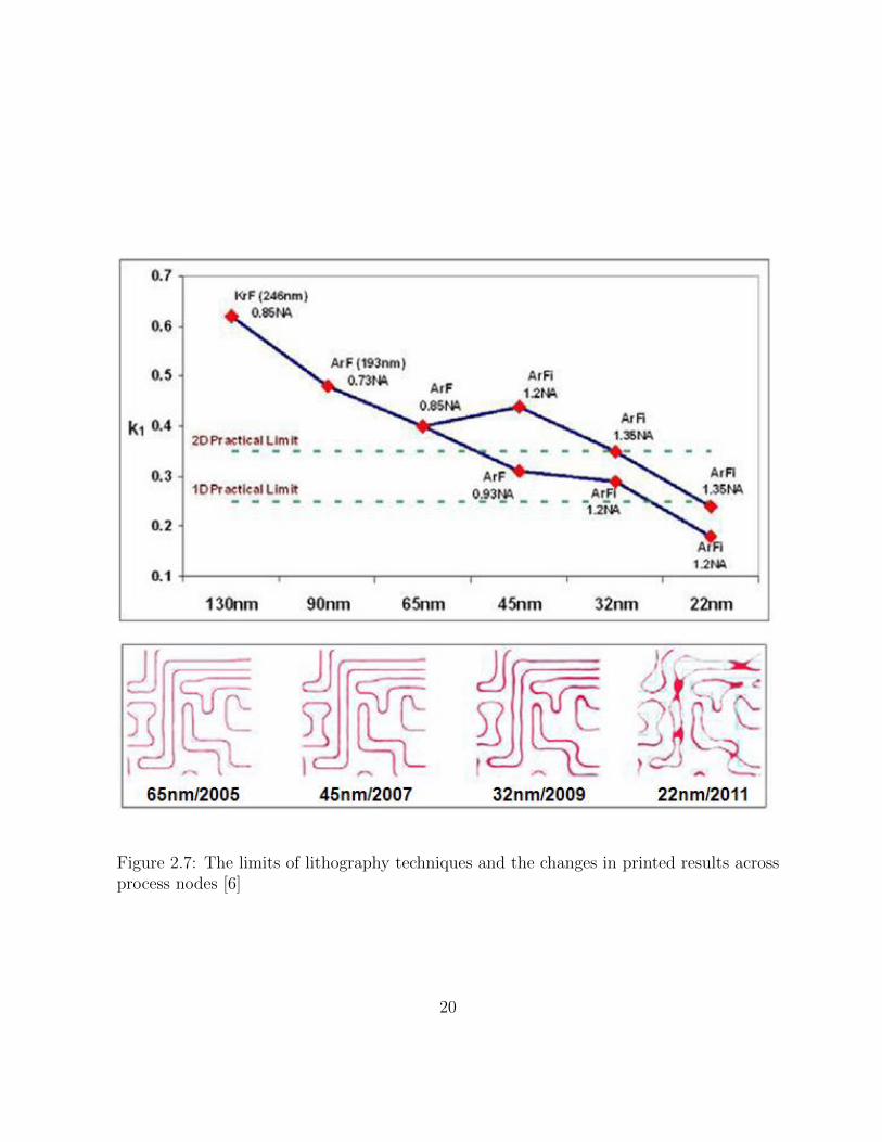
Figure 2.7: The limits of lithography techniques and the changes in printed results acrossprocess nodes [6]
20
Vth ≈ Vth0 − (ζ + ηVDS)e−L/λ (2.3)
where η is the DIBL effect coefficient, and Vth0 is the long channel threshold voltage.Therefore, a slight variation in channel length will introduce large variation in Vth,as shownin Figure 2.8.
Figure 2.8: Measured Vth versus channel length L for a 90nm which shows strong shortchannel effects causing sharp roll-off for Vth for shorter L.[4]
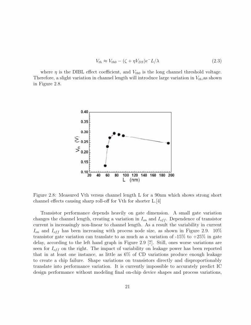
Transistor performance depends heavily on gate dimension. A small gate variationchanges the channel length, creating a variation in Ion and Ioff . Dependence of transistorcurrent is increasingly non-linear to channel length. As a result the variability in currentIon and Ioff has been increasing with process node size, as shown in Figure 2.9. 10%transistor gate variation can translate to as much as a variation of -15% to +25% in gatedelay, according to the left hand graph in Figure 2.9 [7]. Still, ones worse variations areseen for Ioff on the right. The impact of variability on leakage power has been reportedthat in at least one instance, as little as 6% of CD variations produce enough leakageto create a chip failure. Shape variations on transistors directly and disproportionablytranslate into performance variation. It is currently impossible to accurately predict ICdesign performance without modeling final on-chip device shapes and process variations,
21
especially from 90nm technologies downwards. However, for predictable silicon success,these shape and process variations must be predicted and taken into account early in thedesign process [49].
Figure 2.9: Ion and Ioff variations due to transistor length [7]
Topography variations
Chemical mechanical polishing (CMP) is performed between lithography steps to attainthe designed layer height and to planarize the layer for successive process steps. Un-fortunately, CMP is imperfect and cannot eliminate topography variation. Topographyvariation changes the metal height in back-end of the line (BEOL) which affects the wireresistance and capacitance. CMP for front-end of the line (FEOL) is used to planarize theoxide that is deposited for STI. Imperfect FEOL CMP leads to defocus during polysiliconpatterning and poor inter-device isolation.
Topography variation is understood to be partly systematic for both FEOL [3] andBEOL [34]. Another example is gate oxide thickness variation which affects gate-tunnelingleakage and device subthreshold slope. Gate oxide is manufactured by light oxidation andits thickness variation, though small, is considered random.
22
Interconnect parasitics are significant and complex components of circuit performance,signal integrity and reliability in IC design. Copper/low-k process effects are becomingincreasingly important to accurately model interconnect parasitics. Sub-90nm intercon-nects with their narrow and tall (Z-plane) configurations create significant variations inthe Z-plane, which, when added to the X-Y variations due to RET, have a large impacton parasitics.
These variations are amplified because metal sheet resistance varies as a nonlinearfunction of line width, as shown in Figure 2.10. Copper resistivity rises dramaticallybelow 90nm due to increased electron scattering on grain boundaries and interfaces. Thisphenomenon causes significant systematic changes in sheet resistance as a function of linewidth. If line width cannot be predicted accurately, the result is inaccurate resistance anddelay prediction.
According to ITRS roadmap, copper dishing/erosion after Chemical-Mechanical Pol-ishing (CMP) and scattering effect may increase resistance significantly. Also, couplingcapacitance between wires becomes dominant over ground and fringing capacitance at0.18um technology (over 60% of the total capacitance), and increases rapidly with higherwire aspect ratio of the advanced technologies [50], [51],[52]. Therefore, interconnect delaywill suffer from the increased resistance and coupling capacitance more seriously in thefuture [53].
Material variations
The STI stress effect is depicted in Figure 2.5. It has been shown that the residual stressand corresponding shift in electrical performance can be qualitatively described by twogeometric parameters, SA and SB [36], [37] (Figure 2.11). These represent the distancefrom the gate to the edge of the OD on either side of the device. MOSFET parameters suchas Vth, peak gm and Idsat have been shown to vary linearly with the following function,
Stress =1
SA + L2
+1
SB + L2
(2.4)
This relationship has been incorporated into existing SPICE models [9] to allow thisphenomenon to be included in circuit simulations.
Stress due to STI is compressive and typically enhances the mobility of PMOS whiledegrading the mobility of NMOS. Consequently, delay and leakage increase for PMOS whiledecreasing for NMOS. Several techniques have been proposed to reduce STI stress-induced
23
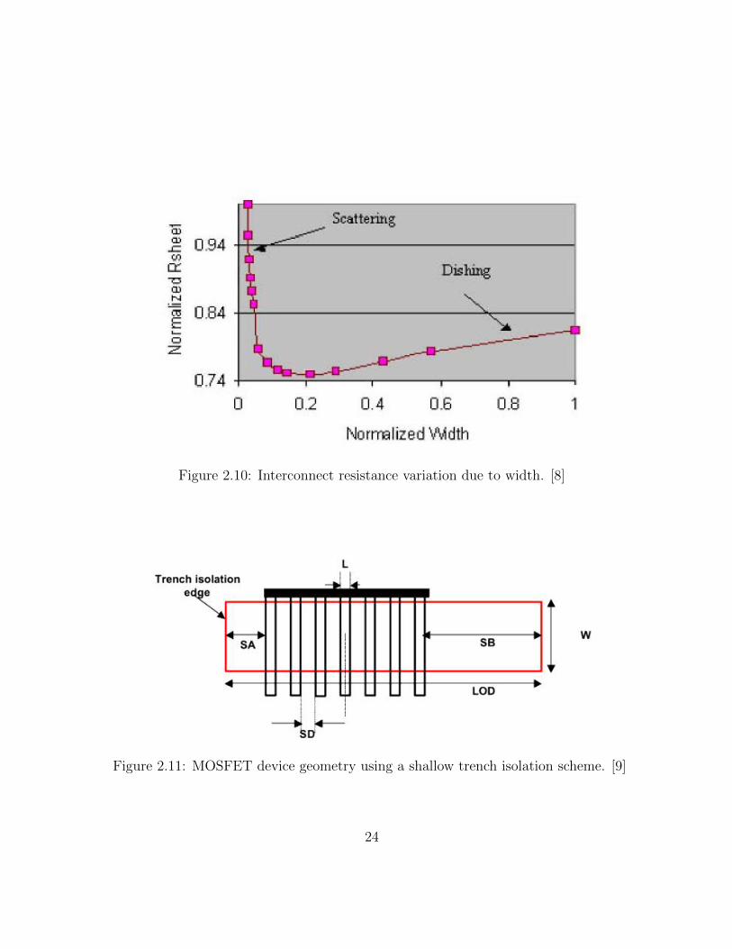
Figure 2.10: Interconnect resistance variation due to width. [8]
Figure 2.11: MOSFET device geometry using a shallow trench isolation scheme. [9]
24
variation [54]. STI stress is highly systematic and is partly modeled in today’s design flows.Recent works have proposed modeling the residual STI stress effects [55].
In addition, material variations cause variations in carrier mobility, polysilicon resis-tance, etc. Dopant concentration in the device channels affects the threshold voltage andconsequently subthreshold leakage and device delay. Due to the small number of dopantatoms in the channel in modern devices, dopant density varies significantly and randomlyas a percentage and induces substantial random variation in threshold voltage. The impactof well proximity on the threshold voltage (Vth) of the nMOS device is shown in Figure2.12. The Vth is found to increase by as much as 50mV as the device moves closer to thewell edge which is consistent with previous observations [40],[43].
Figure 2.12: Vth versus well-edge distance for 3.3V nMOS device.[5]
As a consequence of these manifestations, a significant variation is seen in circuit delayand leakage. With technology scaling, process variations are increasing as a percentage,and consequently the delay and leakage variability is increasing. There is considerableparametric yield loss today especially during yield ramp-up phase causing substantial valueloss.
25
2.4 Design for Manufacturing
While DFM has attracted great deal of attention recently from industry and academia,several techniques that can be arguably be considered DFM techniques have been in usefor several years.
Design for Manufacturing (DFM) refers to measures taken during the design processto enhance yield. Parametric yield enhancement facilitated by DFM can contribute toimprovement of design performance and/or power, and/or designer productivity. DFMtechniques can compensate for, reduce, or make the design more robust to various typesof manufacturing non-idealities.
2.4.1 Traditional DFM Methods
Traditionally, design and manufacturing have been conveniently kept separated, with onlyminimal information exchange. One traditional DFM category is a technique that controlsthe design implementation to make it more robust to various types of manufacturing non-idealities. Typically, these techniques are on the physical layout level. Examples of thesetechniques are:
• Design rule checking (DRC). Design rules have been the primary method for thefoundry to convey manufacturing limitations to design. Design rule checking, verifiesadherence to these rules, and a design that is design rule correct is expected to havea high functional and parametric yield. Simple examples of DRCs are minimumspacing, minimum and maximum dimension or area, and minimum and maximummetal density.
• Restricted design rules (RDR). The basic concept behind restricted layout is to limitwhat the designer is allowed to do. Designers want a wide assortment of possiblefeatures or shapes or constructs that they are allowed to use. Conversely, the fabwould like a very limited set of what the designer is allowed to useideally, every-thing would be perfectly regular and repeatable, making designs much more simpleto process and much more robust against manufacturing variability. For example,lithographic rounding of both the active and the contact in a source or drain con-nection can reduce the alignment marginality, creating the potential for a resistivecontact. In a gate construct, horizontal bends in the field poly near the gate caninduce an inherent systematic variation in the L-effective on the corner of the gate.With misalignment, that variation can be quite dramatic, causing the device in this
26

transistor to have more variation in terms of drive current, leakage, etc. Similarly,because of a horizontal-to-vertical transition in the active layer, this curvature cancause variation in the W-effective, affecting the drive strength, among other aspects.With alignment variability, this effect will vary dramatically as well.
The restricted design compromise is to have some assortment of allowable featuresor constructs, but a much smaller list and a more controlled list than what has beenallowed in the past. With restrictive design, future designs will be much more regularthan current designs, and therefore actually manufacturable.
Another category, are DFM techniques that account for various types of manufacturingnon-idealities during the front end design phase. Typically, these techniques are on theelectrical level of abstraction. Examples of these techniques are:
• Guardbanding. Considerable margin is allocated during design to account for processvariations. Today’s timing and power analysis flows are corner-based, i.e., a set ofconservative process, voltage, and temperature (PVT) settings are assumed in anal-ysis. With respect to process variations, hold and setup time checks are performedat fast and slow process corners respectively. Leakage is typically highest at the fastprocess corner, but the use of typical process corner to reduce pessimism in analysisis common. The premise behind corner-based flows is that if the design meets itsspecifications at conservative PVT settings, it will meet them at all other conditions.Unfortunately, this premise is not true and is now breaking down due to complexdependence of electrical metrics on variations. For example, shorter gate lengths donot necessarily have higher leakage (due to reverse short channel effect), and widerwires are not necessarily faster. The above techniques were relatively easy to adoptand served well until the 130nm node. Since then, as the complexity and extent ofprocess variations has increased, these techniques, while remaining necessary, are nolonger sufficient.
Several problems stem from the inadequacy of these techniques and call for novel DFMtechniques that explicitly target yield enhancement.
• With scaling, as process variations have become complex and large, design rulesare no longer able to capture the variations completely and precisely. In moderntechnologies, layout regions that do not meet design rules may yield well, while thosethat meet them may not. Thus, design rules have become extremely complex in anattempt to capture process variations that arise due to complex layout configurations.
27
Recommended design rules, which are preferably but not necessarily required to bemet, have also been introduced. A large set of design rules poses maintainabilityproblems, and limits the freedom of optimization algorithms and tools in physicaldesign.
• The use of restricted design rules (RDRs) [56], for example those that enforce regu-larity by allowing only one or two pitches, increases the chip area.
• Corner-based analysis assumes conservative process conditions; this is overly pes-simistic since all parameters have an extremely small likelihood of being at theirconservatively assumed values at the same time. Moreover, the design metric un-der analysis may have a non-monotonic dependence on process parameters, in whichcase worst-casing the process parameter will not result in worst-casing of the designmetric. To reduce pessimism and improve worst-casing of design metrics, analysis isperformed at a large number of corners. Unfortunately, the number of corners cangrow rapidly with process parameters and the analysis can be both pessimistic andrisky at the same time [57]. Furthermore, corner-based methods cannot account ad-equately for inter-die variations since all components are assumed to be at the sameprocess corner. A notable exception is on-chip variation analysis which allows clockand data path components to be at opposite corners.
• As guardbanding increases and compromises the advantages from scaling, designersare under tremendous pressure as they seek to meet market expectations. To im-prove delay, power, and area of the design, considerably more time must be spent oniterations and fixing violations. This reduces productivity.
• Design rules and guardbanding can no longer be sufficiently pessimistic to ensure highparametric yield. Unexpectedly large variations and failures can cause intolerableyield loss, and require costly design re-spins.
2.4.2 Taxonomy
To really bridge the gap between design and manufacturing, it is important to modeland feed proper manufacturing metrics and cost functions upstream to the design side.Model based DFM techniques can be broadly classified into the following two categoriesdepending on the yield loss component that they address.
1. Functional yield enhancing. Process-based, or sometimes referred as physicalDFM technology, is concerned with identifying and correcting particle defects or
28
process variations that can lead to functional failures like shorts and opens. Severalmodel-based techniques have been proposed to make the design robust to random andsystematic variations. As for random contamination-caused defects and large processvariations, critical area analysis [58] finds the chip areas that have a high chance ofcausing functional failures under an assumed contaminant particle size distribution.For systematic variations, hotspot detection [59] flags chip areas that are vulnerableto large variations due to lithography non-idealities.
Examples of corresponding design enhancements include wire spreading, wire widen-ing, and via doubling. Physical DFM also implements geometric yield improvementwith recommended rules. Functional yield enhancement techniques are simpler andeasier to adopt because they are primarily shape-centric and have limited or no in-teractions with electrical metrics such as delay and power. Physical DFM is animportant technology, especially during the early stages of new process development,when low functional yield is the primary obstacle to process qualification. The nextcritical milestone in nanometer design is the creation and validation of transistor andinterconnect models that are accurate enough to ensure that predicted versus actualcircuit performance supports design objectives, reduced costs, and increased productfunctionality.
2. Parametric yield enhancing. Parametric-related yield losses are caused by vari-ations in electrical properties. As the physical DFM technologies are familiar tomanufacturing and CAD personnel responsible for ensuring designs meet the basic re-quirements for manufacturability. In slight contrast, parametric-based, or sometimesreferred as electrically-based DFM, is the knowledge that can be gained from themanufacture and critical to designers who must ensure that designs meet datasheetperformance specifications and competitive yield targets. These techniques have at-tracted great interest recently as they address an ever-increasing and now dominantyield loss component. The objective of these techniques is to contain the variabilityin delay and leakage. This thesis focuses on such DFM techniques.
As illustrated in Figure 2.13, parametric yield enhancing techniques can be summarizedas follows: starting with modeling and accounting for systematic variations followed byDFM techniques either for:
• Process Variation Reduction.
or
• Systematic Variation-Aware Analysis and Design Enhancement.
29
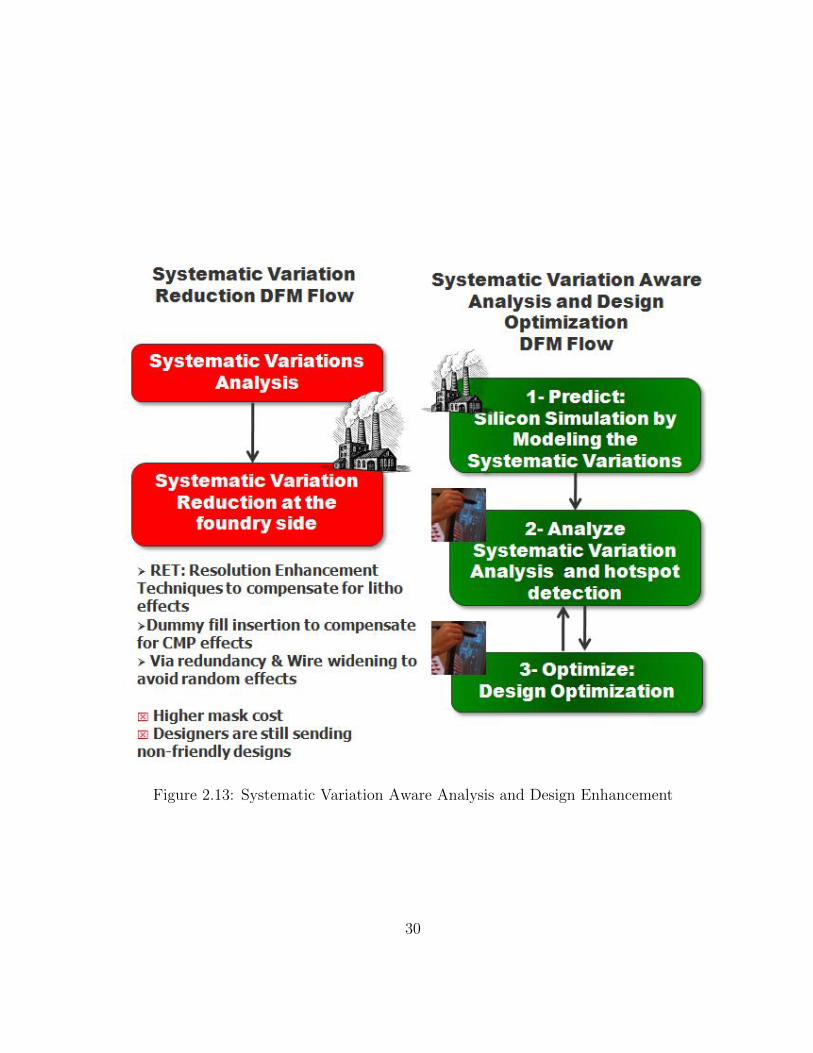
Figure 2.13: Systematic Variation Aware Analysis and Design Enhancement
30
Process Variation Reduction
1. Reducing Random Particle Defects: Random particle defects are a fact of ICmanufacturing, but the number and severity of these defects increases as layout fea-tures and the space between them continue to shrink. Recommended design rulesuse manufacturing information to suggest spacing’s that reduce the overall chancesof random particle defects. However, recommended rules can generate thousands ofrule violations, with no information to help you decide which ones are most criti-cal. Critical area analysis (CAA) uses manufacturing information about the processparticle sizes and probability distribution to identify specific areas of an integratedcircuit layout with a higher than average vulnerability to random particle defects.
2. Reducing Lithography Variation: After modeling the lithography process, RETsare used as the primary methods to reduce lithography variations. As explainedearlier, the purpose of these techniques is to minimize the lateral distortion betweenthe drawn and the on-silicon shapes. Typically, RETs are transparent to the designphase and are performed after signoff. However, modifications can be made to circuitsthat make them more amenable to RETs, such that the RETs achieve strongerreduction of lithography variation.
3. Reducing Planarity Variation: The impact of chemical mechanical polishing(CMP) is inherently pattern-dependent. Whether a feature is isolated or located ina dense array affects both polishing time and results. Likewise, circuit performanceis also affected by how the physical layout reacts to CMP. Controlling both thicknessand capacitance variation is a balancing act. Several industrial tools can model andsimulate the CMP process, based on that dummy fill insertion and slotting techniquesare introduced. Dummy fill insertion and slotting are the primary design techniquesused today to aid planarity by altering the density. For signal wires that are routedby gridded routers, metal density typically does not exceed nearly 50% because inter-wire spacing is nearly equal to the wire width; for these wires, slotting is not required.Slotting is done for special wires such as power/ground rails and is less desirable thanfill insertion [60]. Fill insertion is the mainstream technique to increase density bothfor FEOL CMP [3] and BEOL CMP [34].
Systematic Variation Aware Analysis and Design Enhancements
To really bridge the gap between design and manufacturing, DFM must due the followingtwo jobs: First, bring manufacturing awareness up into the design flow. Second, communi-
31
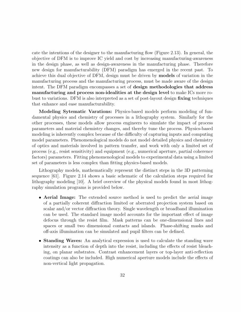
cate the intentions of the designer to the manufacturing flow (Figure 2.13). In general, theobjective of DFM is to improve IC yield and cost by increasing manufacturing-awarenessin the design phase, as well as design-awareness in the manufacturing phase. Thereforenew design for manufacturability (DFM) paradigm has emerged in the recent past. Toachieve this dual objective of DFM, design must be driven by models of variation in themanufacturing process and the manufacturing process, must be made aware of the designintent. The DFM paradigm encompasses a set of design methodologies that addressmanufacturing and process non-idealities at the design level to make ICs more ro-bust to variations. DFM is also interpreted as a set of post-layout design fixing techniquesthat enhance and ease manufacturability.
Modeling Sytematic Varations: Physics-based models perform modeling of fun-damental physics and chemistry of processes in a lithography system. Similarly for theother processes, these models allow process engineers to simulate the impact of processparameters and material chemistry changes, and thereby tune the process. Physics-basedmodeling is inherently complex because of the difficulty of capturing inputs and computingmodel parameters. Phenomenological models do not model detailed physics and chemistryof optics and materials involved in pattern transfer, and work with only a limited set ofprocess (e.g., resist sensitivity) and equipment (e.g., numerical aperture, partial coherencefactors) parameters. Fitting phenomenological models to experimental data using a limitedset of parameters is less complex than fitting physics-based models.
Lithography models, mathematically represent the distinct steps in the 3D patterningsequence [61]. Figure 2.14 shows a basic schematic of the calculation steps required forlithography modeling [10]. A brief overview of the physical models found in most lithog-raphy simulation programs is provided below.
• Aerial Image: The extended source method is used to predict the aerial imageof a partially coherent diffraction limited or aberrated projection system based onscalar and/or vector diffraction theory. Single wavelength or broadband illuminationcan be used. The standard image model accounts for the important effect of imagedefocus through the resist film. Mask patterns can be one-dimensional lines andspaces or small two dimensional contacts and islands. Phase-shifting masks andoff-axis illumination can be simulated and pupil filters can be defined.
• Standing Waves: An analytical expression is used to calculate the standing waveintensity as a function of depth into the resist, including the effects of resist bleach-ing, on planar substrates. Contrast enhancement layers or top-layer anti-reflectioncoatings can also be included. High numerical aperture models include the effects ofnon-vertical light propagation.
32
Figure 2.14: Flow diagram of a lithography model [10]
33

• Prebake: Thermal decomposition of the photoresist photoactive compound duringprebake (also called post apply bake) is modeled using first order kinetics resultingin a change in the resist’s optical properties. Many important bake effects, however,are not yet well understood.
• Exposure: First order kinetics are used to model the chemistry of exposure. Bothpositive and negative resists can be simulated.
• Post-Exposure Bake: A two-dimensional or three-dimensional diffusion calculationallows the post-exposure bake to reduce the effects of standing waves. For chemicallyamplified resists, this diffusion is accompanied by an amplification reaction whichaccounts for crosslinking, blocking, or deblocking in an acid catalyzed reaction. Acidloss mechanisms and non-constant diffusivity can also be simulated.
• Development: Kinetic models for resist dissolution are used in conjunction with anetching algorithm to determine the resist profile. Surface inhibition or enhancementcan also be taken into account. The combination of the models described aboveprovides a complete mathematical description of the optical lithography process.Use of the models incorporated in a full lithography simulation package allows theuser to investigate many interesting and important aspects of optical lithography.
• Etching: To cope with the effect of edge topography on device characteristics, dueto the high integration of VLSI’s, accurate three-dimensional (3D) topography sim-ulation models are required [61].
Analyzing systematic variations and detecting hotspot: Process variations canbe observed at the topological or the electrical level. The topological level refers to theshape and physical attributes of the devices, including critical dimension (CD), minimumpitch and pattern density. Depending on the topological change, the electrical behavior canbe affected if the variations occur in electrically sensitive areas of the design (e.g., polysil-icon gate width differences between a pair of matched transistors, or narrowing of longmetal lines that subsequently increase resistance). At the same time, topological changesinduced by some types of dummy fill, short interconnect paths or non-critical corners ofdiffusion layers will not present any observable differences in the electrical behavior of thedevices. Until now, only shape-centric parameters such as fidelity (achieved by aggressiveRET) and pattern robustness (achieved by manufacturing-aware design) have been con-sidered in the manufacturability of designs. However, other processing effects that are lessdependent on shape or structure can also contribute to the final operation of the electronicdevices. For example, even when poly gate widths are perfectly matched and robustly
34
built, processing steps such as ion implantation, diffusion or material selection can makean otherwise correct design fail.
With the former paragraph in mind, the scope of this work is to apply relevant DFMprinciples to quantify some electrical variables that shape and topology have on the elec-trical behavior of devices.
Design Enhancement: DFM is an art of balance to accomplish multiple goals suchas high die yield, aggressive product performance, and zero reliability fallouts, which areoften loosely tied or even incompatible. In that role, DFM has to rely on cross-disciplinaryenhancement techniques, which deal with multiple design, manufacturing and productissues. Therefore, it requires a multi-objective optimization approach [62]. At the sametime, DFM has limited resource base, as it should operate within the predetermined diearea, product schedule, circuit timing budget, and design effort and yet make a positivedifference. DFM enhancements need a lot of heavily processed information, e.g., in theform of litho, yield, or device models and the results of their implementation hinge on theaccuracy of these models. From this perspective, one can divide recent DFM enhancementtechniques into three groups aligned with the stage of their introduction in design cycle:
1. Design and process definition stage. At the earliest design definition stage, DFMaligns with the generic methodology of IC design rules and guidelines. Here, newDFM concepts emerge as correct-by-construction architecture at single cell level [63].To assist the process, layout tolerance bands are introduced to help preserve designintent, i.e., ensure the expected electrical performance [64].
2. Design execution stage, correct-by-construction is also proposed, this time for multi-cell IP (e.g., modular design of multi-port cells [65]), die level routing [66], and then,at mask level [67]. For the complete IC layout, the new concepts on how to validatedesign data, mask data, or both [68], emphasize process proximity correction forsingle or multiple layers [69] and [70].
3. Finally, at the latest DFM verification stage, enhancement techniques are used toenhance manufacturing feedback to design/layout by correcting local yield limiters(hot spots, [67], [68], [69], [70], [71]). DFM verification techniques based on inspectionor simulation, involve methods, systems, EDA algorithms, computer programs, anddesign kits [69], [70], [71], [72], [73], to improve circuit performance before more masksets are built for the manufacturing line. After the improved design is placed in thefab, data collection systems need to provide feedback e.g., from defect detection [74].
35

2.5 Summary
Variations in the IC manufacturing process are manifested as
1. Deviation from the intended shapes of IC geometries, and
2. Variations in impurity (i.e., dopant) concentrations.
These variations are composed of systematic and random components. The systematiccomponent of variation can be attributed to specific sources in the manufacturing pro-cess, while the random component is usually a result of confounding of several sources ofvariation and cannot be attributed to specific sources. A significant fraction of the totalvariation in shapes of IC geometries is systematic in sources such as focus, exposure dose,lens aberrations, during the lithography process. Mechanical stress and CMP processesare additional sources of process systematic variations. The primary goal in the associ-ated research is to develop CAD solutions that can drive systematic variation-aware designanalysis and enhancement.
36
Chapter 3
A Methodology for AnalyzingProcess Variation Dependency onDesign Context and the Impact onCircuit Analysis
3.1 Introduction
As VLSI technology scales down towards 65nm and below, performance of integrated cir-cuits is increasingly affected by fabrication variations. Moreover the fabrication variationsat these advanced IC technologies are highly dependent on the physical layout and re-cently more dependent on proximity effects of this layout from neighboring cells. In anormal design process; designers only deal with schematics design entry or front end HighDescription Languages (HDL) digital codes. In this design entry phase, no layout infor-mation is available for the front end designers. This is acceptable in the IC technologiesabove 65nm; where most of the required layout or back end information is captured in thefront end entry, so the layout shape has minimal impact on the original design. However;this is no more acceptable in the new advanced IC nanometer technologies; more and morelayout parameters are now impacting directly the transistors performance. This makes thefinal fabricated IC performs differently from the original design, unless these layout effectsand variations are to be considered earlier in the design cycle.
As an example, mechanical stresses induced by Shallow-Trench Isolation (STI) on thegate channel can alter the drive current of NMOS and PMOS transistors up to 20% de-
37
pending on the length of diffusion (LOD) [37] [75]. As a consequence, the drive currentof a transistor is not only related to the parameters of the gate such as the gate length Land gate width W but also is related to the exact layout shape of the individual transistor.Similarly the lithography printability is strongly layout dependent [76]. As the densityof VLSI circuit increases the proximity effects are becoming a significant consideration todesign layout linewidth control in range of nano-meters using current state-of-the-art pho-tolithography tools that operate with deep ultraviolet (DUV) light wavelengths of 193nm.Optical light rays in the photolithography process diffract and pass through the reticle in adifferent matter based on the layout context and mask pattern density, and hence impactthe final Critical Dimension (CD) printability on wafer.
Therefore, when designing a standard cell or characterizing its electrical behavior priorto use in a chip implementation flow, it is important to know the impact of layout context-dependent manufacturing variations on the cells parametric views. Traditional standardcell characterization treats the cell in complete isolation from its context. This is somehowaccepted for older technologies. However in advanced nano-IC technologies at 65nm andbelow this is not the case. During standard cell design, it is recommended to have a context-dependent parametric analysis that can be used to improve the cell layout and architectureso that variability is minimized. The proposed CAD tool presents a methodology to predictthe impact of context-dependent systematic manufacturing variations on the parametricbehavior of standard cells in an integrated circuit. Such a methodology can be appliedto the analysis of a full chip composed of standard cell components, and reports layoutcontext-dependent changes in chip timing and power. For lithography and stress variability,a study on 65nm, 45nm standard cell libraries and mid-size designs is done to examine theinfluence of cell context when looking at gate CD and the design performance. A contextgenerator engine is implemented to study the effect of the design context variation. Thisengine has several user defined parameters to enable the user to simulate various contextconditions.
The rest of this chapter is organized as follows: Section 3.2 presents the availablesolutions that analyze process variation and studies the impact on circuit performance.Section 3.3 discusses the stress and lithography variation dependence on design context.Section 3.4 depicts the proposed characterization methodology entailed in implementingthe engines used in our flow. In order to verify the usefulness of our proposed methodology,industrial standard cell context-aware characterization is performed. Impact on electricalparameters will be examined on the context-aware standard cells and results are highlightedin Section 3.5.
38
3.2 Background
One of the major challenges facing semiconductor companies today is how to increaseyield. Since yield is directly related to profitability, by predicting and improving yieldbefore tapeout, an IC designer can have a direct dollar impact on the success of his design.The ability to predict and improve yield becomes even more vital as processes move togeometries under 100 nanometers. In fact, there are discouraging predictions that yields forICs with geometries below 100 nanometers may not exceed 50 or 60 percent [77]. To accountfor process variations, an IC designer not only has to design for good electrical performance,but also for high manufacturing yield [78]. Electronic Design Automation (EDA) companiesneed to develop tools and methodologies that designers can easily incorporate into theirflows to meet this challenge. There are many factors that affect yield. Physical problemsthat are highly dependent on layout can effect yield. Manufacturing issues such as defectdensity on the silicon, maturity of the process, and effectiveness of design rules also affectyield. Another factor, and the main topic of this chapter, is how the design will react toprocess variations, mainly speaking about systematic variations such as lithography, stressand CMP. The designs sensitivity to these variations is called parametric yield. Increasingparametric yield is a challenge within a designers realm. There are currently several tools,or analyses, that a designer may use to check the design for process variations. This sectionprovides a brief description of the commonly used methods, including corners simulation,Monte Carlo analysis, response surface modeling.
3.2.1 Corners Simulation
Corners simulation is perhaps the most widely used method to test for process variations.With this method, a designer determines the worst case corners, or conditions, underwhich the design will be expected to function. The modeling group may provide thecorners for the process. Next, each corner is simulated, and the output of each corneris examined to determine whether or not the design performs as required under each ofthe specified conditions. There are a number of issues with corners analysis. Perhapsthe most troublesome of these is if the corners are not provided, then the designer maynot know what the corners actually are, leading him to frequently make a best guess.Guessing worst case corners that will never occur in reality not only wastes design time,but also can result in a design that takes more area or consumes more power than needed,or even becomes impossible to design. Not guessing corners that will occur in reality mayresult in lower yield. The advantage of corners analysis is its relative simplicity. Cornersanalysis is neither compute-intensive nor time consuming (as compared to Monte Carlo
39

analysis, for example). To correct failed corners, a designer can run a sensitivity analysisor optimization on the failed corners, hoping that the other corners continue to pass.
3.2.2 Monte Carlo Analysis
Although the guess work in determining the worst case corners is removed with MonteCarlo analysis, the distributions of the parameters are still required. Whereas cornersanalysis produces a binary outcome (either the corner passes or fails), Monte Carlo analysisproduces samples of a continuous function that can be used to estimate yield. In addition,Monte Carlo deals with the distributions of the process parameters among lots, wafers, anddies, and allows the designer to study the effect of parameter variations among devices onthe same chip. With Monte Carlo analysis, hundreds of simulations are typically run witha variety of variations introduced randomly. However, the stdev (confidence interval) of aMonte Carlo yield estimate is proportional to 1/sqrt(n) where n is number of simulations.A Monte Carlo run of 100 to 200 simulations is very time consuming. Most of the time,it is not feasible to even run this many simulations, thereby introducing a sampling error.This means that one Monte Carlo run may generate a yield of 82 percent while another runmay generate a yield of 85 percent, with no change to the design. Even worse, a designermay see an initial yield of 82 percent, tweak some parameters, rerun, and see a yield of 85percent. At this point, the designer may not know if the increased yield was due to thechange in the design parameter or because of the Monte Carlo sampling error. Anotherdisadvantage of Monte Carlo is that all changes to design variables intended to improveyield will result in a complete rerun of the entire Monte Carlo analysis. So, although MonteCarlo eliminates the guesswork found in corners simulation, Monte Carlo simulations arevery time consuming and do not run enough simulations to avoid sampling errors.
3.2.3 Response Surface Modeling
Response surface modeling (RSM) is the answer to the time-consuming sampling errorspresented by Monte Carlo. RSM reduces the 1/sqrt(n) error from Monte Carlo and allowsthe user to reduce the sampling error to nearly zero. With RSM, a set of polynomial mod-els are created from about 20 to 50 simulations (design of experiments) that approximatethe original design. These models are run tens of thousands of times with the same ran-dom variations used during Monte Carlo analysis. Since a significantly larger number ofsimulations are run, the sampling error is reduced to nearly zero. With the design replacedby polynomial models, the designer can run the thousands of simulations much faster the
40
time is reduced to a matter of seconds as opposed to days. RSM is not, however, withoutits problems. The error introduced with this technique is clearly the difference betweenthe polynomial models and the original design. Additionally, running the simulations onthe original design (design of experiments) can be time consuming, because the number ofsimulations required is highly dependent on the number of statistical parameters (which isa major downfall compared to Monte Carlo analysis).
3.2.4 Issues with the Previous Process Analysis Tools
Despite their problematic aspects, Monte Carlo analysis and RSM are a big step forwardfrom corners simulation in predicting parametric yield. However, most designers continueto use corners analysis most of the time. The main reasons are lack of statistical models(needed for Monte Carlo analysis and RSM), lack of tools to create the models for RSM,time constraints, and, most often, company policies. Beside the above issues, underlyingthe use of corner-based methods is the assumption that sufficient guard-bands or pessimismin the modeling and the timing analysis stages will ’guarantee’ a working design. Whileover-design is an option, it ignores the competitive pressures to build a faster, lower-powerand smaller silicon chip than another IC vendor, and essentially takes a new design back toan earlier generation silicon node. And finally, these pessimistic, over-constrained designs,surprisingly can still fail in production silicon because the outliers have not been analyzed.On top of that, all these analysis are done before the physical layout is implemented.
Layout-dependent variations, can cause two different layouts of the same device tohave different characteristics even when the two instances are located close to each other.Layout-dependent variations are different from random ones because they are predictableand can be modeled as a function of deterministic factors such as layout structure andthe surrounding topology. Process variation can be caused by many sources with eachexhibiting a different dependence on layout and design parameters. One must identify,characterize, and model all sources of variation for better model-to-hardware correlation.
The proposed CAD solution presents an automated methodology to predict the actualimpact of physical layout-dependent systematic manufacturing variations on the paramet-ric behavior. Before presenting this methodology, the stress and lithography variationdependence on design context will be discussed first.
41
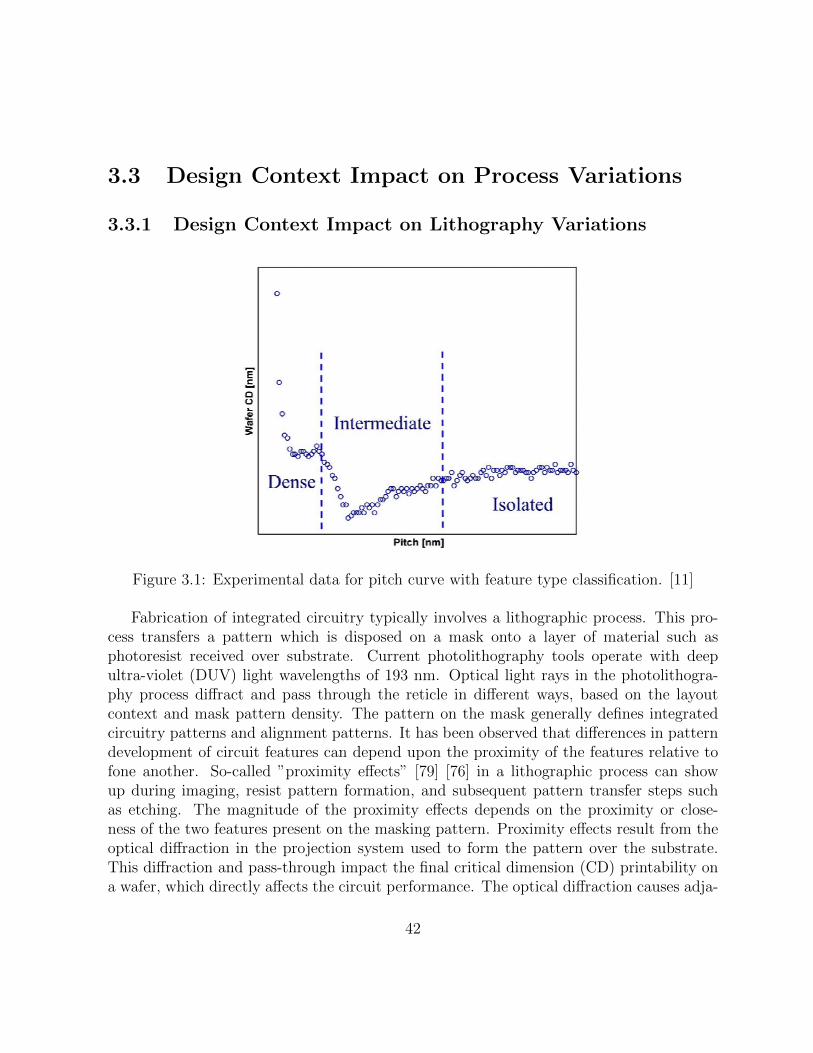
3.3 Design Context Impact on Process Variations
3.3.1 Design Context Impact on Lithography Variations
Figure 3.1: Experimental data for pitch curve with feature type classification. [11]
Fabrication of integrated circuitry typically involves a lithographic process. This pro-cess transfers a pattern which is disposed on a mask onto a layer of material such asphotoresist received over substrate. Current photolithography tools operate with deepultra-violet (DUV) light wavelengths of 193 nm. Optical light rays in the photolithogra-phy process diffract and pass through the reticle in different ways, based on the layoutcontext and mask pattern density. The pattern on the mask generally defines integratedcircuitry patterns and alignment patterns. It has been observed that differences in patterndevelopment of circuit features can depend upon the proximity of the features relative tofone another. So-called ”proximity effects” [79] [76] in a lithographic process can showup during imaging, resist pattern formation, and subsequent pattern transfer steps suchas etching. The magnitude of the proximity effects depends on the proximity or close-ness of the two features present on the masking pattern. Proximity effects result from theoptical diffraction in the projection system used to form the pattern over the substrate.This diffraction and pass-through impact the final critical dimension (CD) printability ona wafer, which directly affects the circuit performance. The optical diffraction causes adja-
42
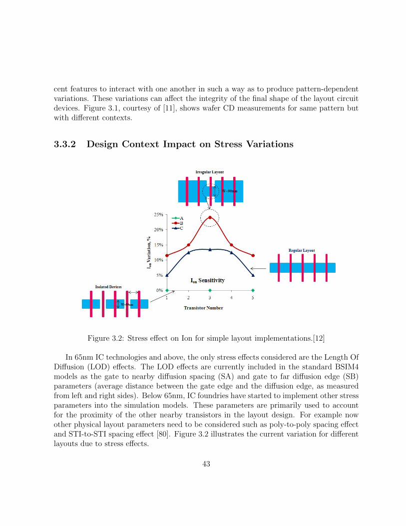
cent features to interact with one another in such a way as to produce pattern-dependentvariations. These variations can affect the integrity of the final shape of the layout circuitdevices. Figure 3.1, courtesy of [11], shows wafer CD measurements for same pattern butwith different contexts.
3.3.2 Design Context Impact on Stress Variations
Figure 3.2: Stress effect on Ion for simple layout implementations.[12]
In 65nm IC technologies and above, the only stress effects considered are the Length OfDiffusion (LOD) effects. The LOD effects are currently included in the standard BSIM4models as the gate to nearby diffusion spacing (SA) and gate to far diffusion edge (SB)parameters (average distance between the gate edge and the diffusion edge, as measuredfrom left and right sides). Below 65nm, IC foundries have started to implement other stressparameters into the simulation models. These parameters are primarily used to accountfor the proximity of the other nearby transistors in the layout design. For example nowother physical layout parameters need to be considered such as poly-to-poly spacing effectand STI-to-STI spacing effect [80]. Figure 3.2 illustrates the current variation for differentlayouts due to stress effects.
43
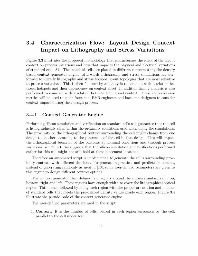
3.4 Characterization Flow: Layout Design Context
Impact on Lithography and Stress Variations
Figure 3.3 illustrates the proposed methodology that characterizes the effect of the layoutcontext on process variations and how that impacts the physical and electrical variationsof standard cells [81]. The standard cells are placed in different contexts using the densitybased context generator engine, afterwards lithography and stress simulations are per-formed to identify lithography and stress hotspot layout topologies that are most sensitiveto process variations. This is then followed by an analysis to come up with a relation be-tween hotspots and their dependency on context effect. In addition timing analysis is alsoperformed to come up with a relation between timing and context. These context-awaremetrics will be used to guide front end, P&R engineers and back end designers to considercontext impact during their design process.
3.4.1 Context Generator Engine
Performing silicon simulation and verification on standard cells will guarantee that the cellis lithographically clean within the proximity conditions used when doing the simulations.The proximity or the lithographical context surrounding the cell might change from onedesign to another according to the placement of the cell in that design. This will impactthe lithographical behavior of the contours at nominal conditions and through processvariations, which in turns suggests that the silicon simulation and verifications performedearlier for this cell might not still hold at these placement locations.
Therefore an automated script is implemented to generate the cell’s surrounding prox-imity contexts with different densities. To generate a practical and predictable context,instead of generating randomly as used in [13], some user-defined parameters are given tothis engine to design different context options.
The context generator then defines four regions around the chosen standard cell: top,bottom, right and left. These regions have enough width to cover the lithographical opticalregion. This is then followed by filling each region with the proper orientation and numberof standard cells that meets the pre-defined density values inside each region. Figure 3.4illustrate the pseudo code of the context generator engine.
The user-defined parameters are used in the script:
1. Context: It is the number of cells, placed in each region surrounds by the cell,parallel to the cell under test.
44
Figure 3.3: Flow used for Extracting Context-aware metrics
45

Figure 3.4: Pseudo Code for the Context Generator Engine
46
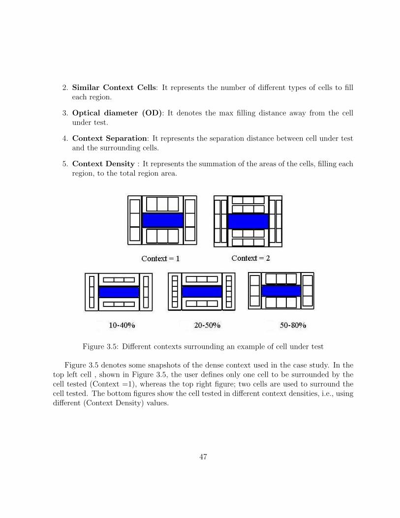
2. Similar Context Cells: It represents the number of different types of cells to filleach region.
3. Optical diameter (OD): It denotes the max filling distance away from the cellunder test.
4. Context Separation: It represents the separation distance between cell under testand the surrounding cells.
5. Context Density : It represents the summation of the areas of the cells, filling eachregion, to the total region area.
Figure 3.5: Different contexts surrounding an example of cell under test
Figure 3.5 denotes some snapshots of the dense context used in the case study. In thetop left cell , shown in Figure 3.5, the user defines only one cell to be surrounded by thecell tested (Context =1), whereas the top right figure; two cells are used to surround thecell tested. The bottom figures show the cell tested in different context densities, i.e., usingdifferent (Context Density) values.
47
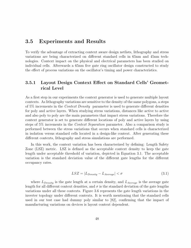
3.5 Experiments and Results
To verify the advantage of extracting context aware design netlists, lithography and stressvariations are being characterized on different standard cells in 65nm and 45nm tech-nologies. Context impact on the physical and electrical parameters has been studied onindividual cells. Afterwards a 65nm five gate ring oscillator design constructed to studythe effect of process variations on the oscillator’s timing and power characteristics.
3.5.1 Layout Design Context Effect on Standard Cells’ Geomet-rical Level
As a first step in our experiments the context generator is used to generate multiple layoutcontexts. As lithography variations are sensitive to the density of the same polygons, a stepsof 5% increments in the Context Density parameter is used to generate different densitiesfor poly and active layers. When studying stress variations, distances like active to activeand also poly to poly are the main parameters that impact stress variations. Therefore thecontext generator is set to generate different locations of poly and active layers by usingsteps of 5% increments in the Context Separation parameter. Also a comparison study isperformed between the stress variations that occurs when standard cells is characterizedin isolation versus standard cells located in a design-like context. After generating thesedifferent contexts, lithography and stress simulations are performed.
In this work, the context variation has been characterized by defining: Length SafetyZone (LSZ) metric. LSZ is defined as the acceptable context density to keep the gatelength under acceptable threshold of variation, depicted in Equation 3.1. The acceptablevariation is the standard deviation value of the different gate lengths for the differentoccupancy rates.
LSZ = |LDensity − LAverage| < σ (3.1)
where LDensity is the gate length at a certain density, and LAverage is the average gatelength for all different context densities, and σ is the standard deviation of the gate lengthsvariations under all these contexts. Figure 3.6 represents the gate length variations in theinverter topology under different contexts. It is worth mentioning that the standard cellsused in our test case had dummy poly similar to [82], confirming that the impact ofmanufacturing variations on devices is layout context dependent.
48
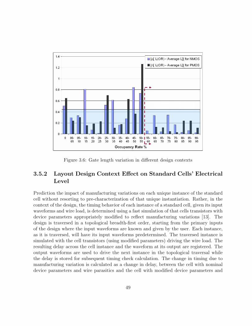
Figure 3.6: Gate length variation in different design contexts
3.5.2 Layout Design Context Effect on Standard Cells’ ElectricalLevel
Prediction the impact of manufacturing variations on each unique instance of the standardcell without resorting to pre-characterization of that unique instantiation. Rather, in thecontext of the design, the timing behavior of each instance of a standard cell, given its inputwaveforms and wire load, is determined using a fast simulation of that cells transistors withdevice parameters appropriately modified to reflect manufacturing variations [13]. Thedesign is traversed in a topological breadth-first order, starting from the primary inputsof the design where the input waveforms are known and given by the user. Each instance,as it is traversed, will have its input waveforms predetermined. The traversed instance issimulated with the cell transistors (using modified parameters) driving the wire load. Theresulting delay across the cell instance and the waveform at its output are registered. Theoutput waveforms are used to drive the next instance in the topological traversal whilethe delay is stored for subsequent timing check calculation. The change in timing due tomanufacturing variation is calculated as a change in delay, between the cell with nominaldevice parameters and wire parasitics and the cell with modified device parameters and
49
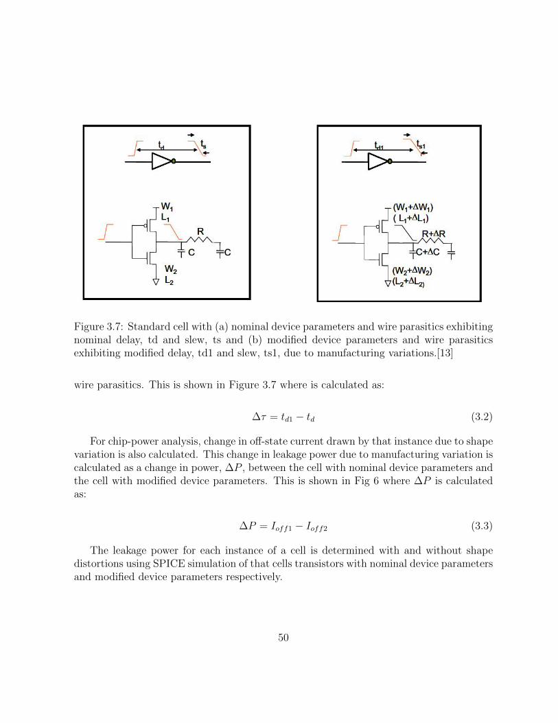
Figure 3.7: Standard cell with (a) nominal device parameters and wire parasitics exhibitingnominal delay, td and slew, ts and (b) modified device parameters and wire parasiticsexhibiting modified delay, td1 and slew, ts1, due to manufacturing variations.[13]
wire parasitics. This is shown in Figure 3.7 where is calculated as:
∆τ = td1 − td (3.2)
For chip-power analysis, change in off-state current drawn by that instance due to shapevariation is also calculated. This change in leakage power due to manufacturing variation iscalculated as a change in power, ∆P , between the cell with nominal device parameters andthe cell with modified device parameters. This is shown in Fig 6 where ∆P is calculatedas:
∆P = Ioff1 − Ioff2 (3.3)
The leakage power for each instance of a cell is determined with and without shapedistortions using SPICE simulation of that cells transistors with nominal device parametersand modified device parameters respectively.
50
Figure 3.8: Standard cell with (a) nominal device parameters drawing leakage current,Ioff1 and (b) modified device considering manufacturing variations drawing leakage current,Ioff2. [13]
Lithography variations impact on Standard Cells’ Electrical Level
After generating contexts around the cell under test, we run Calibre Litho Friendly Design(LFD) tool to create process contours for poly and active. Adjusted values for length andwidth of a transistor are calculated. Multiple styles of formulas are being proposed byEDA [83] . Some are based on creating an L/W value based on either Isat or Ioff [84].Others are based on creating a new Ladj and Wadj.
Additionally, with more advanced tools, contours based on process variation can becreated [85]. With the same technique used for nominal contour based extraction, a morethorough circuit analysis can be accomplished for process window. Performance based sim-ulation of circuits using process variation information has become critical at the nanometertechnologies. In our flow we used the Mentor Contour Simplified Gate (CSG) flow.
After running LFD and CSG, the netlist of the cell’s under test netlist is extracted. TheLdrawn and Wdrawn are replaced by Ladj and Wadj for each transistor. Spice commands thatare used to calculate timing and power values are automatically added in the extractednetlist. The proposed flow generates automatically a table that consists of the simulationresults. Table 3.1 presents an example of the simulated results for a NAND gate.
Simulating the cell’s timing performance through the high-to-low propagation delay(TpHL) and low-to-high propagation delay (TpLH). Figures 3.10 and 3.9 show that be-
51

Table 3.1: Example of the Electrical Simulation Results for NAND gateContext Tplh Tphl P(0,0) P(0,1) P(1,0) P(1,1)
Density% (ns) (ns) (nW) (nW) (nW) (nW)
Isolated 0.15265 0.13458 7.7515 3.77 4.515 0.638Context 0-30% 0.15389 0.13548 7.6767 3.7333 4.472 0.632Context 40-70% 0.148 0.132 7.43 3.61 4.36 0.634Context 70-100% 0.14467 0.12822 7.7219 3.7518 4.5325 0.65676
havior of (TpHL) and (TpLH) are similar to Figure 3.6. As for typical inverters the rela-tion between the high-to-low propagation delay (TpHL) and low-to-high propagation delay(TpLH) is defined by equations 3.4 and 3.5, respectively [86]. If the output load capaci-tance (CL) is independent of the inverter’s size (i.e., the inverter’s intrinsic capacitance isneglected relative to the fanout and wiring capacitance, which was our case) then (TpHL)is inversely proportional to (W/L)n. Similarly, there is an inverse proportional relationbetween (TpLH) and (W/L)p , It is worth mentioning that the NMOS and PMOS gatewidth variations were also monitored with context variation, and compared to the stan-dard deviation. However, the effect of context variation on the transistor gate widths wasminor. This concludes that the variation of (TpHL) and (TpLH) are expected to follow thesame pattern as gate lengths Ln and Lp respectively.
TpHL = 0.52 ∗ CL
(Wn
Ln) ∗Kn ∗ VDSATn
(3.4)
TpLH = 0.52 ∗ CL
(Wp
Lp) ∗Kp ∗ VDSATp
(3.5)
Stress variations impact on Standard Cells’ Electrical Level
To investigate the effect of stress due to context on the behavior of the standard cell, atest case was developed using 45nm technology [87]. A standard cell is extracted thensimulated without context first, then for the same standard cell, a context is generatedaround it then it is extracted using some modified extraction file (extract design onlyunder a marker layer), and then simulated. After that results between the two cases arecompared to find out how the stress due to context is really effective. Results from twocells will be presented; first, is a basic inverter representing a combinational cell, the otherone is a flip-flop, representing a sequential cell .
52
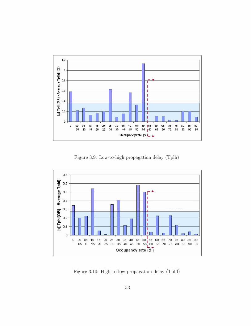
Figure 3.9: Low-to-high propagation delay (Tplh)
Figure 3.10: High-to-low propagation delay (Tphl)
53
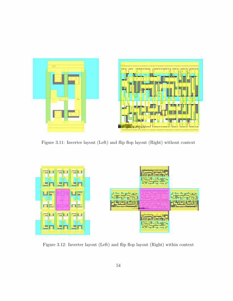
Figure 3.11: Inverter layout (Left) and flip flop layout (Right) without context
Figure 3.12: Inverter layout (Left) and flip flop layout (Right) within context
54
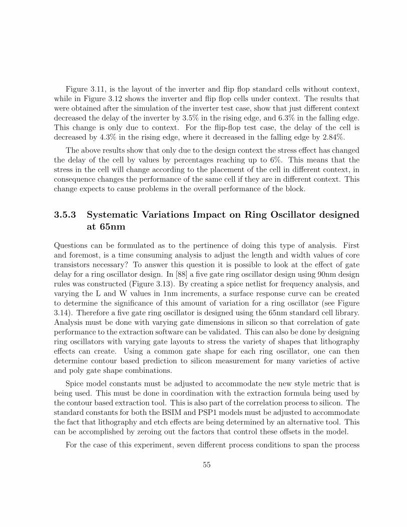
Figure 3.11, is the layout of the inverter and flip flop standard cells without context,while in Figure 3.12 shows the inverter and flip flop cells under context. The results thatwere obtained after the simulation of the inverter test case, show that just different contextdecreased the delay of the inverter by 3.5% in the rising edge, and 6.3% in the falling edge.This change is only due to context. For the flip-flop test case, the delay of the cell isdecreased by 4.3% in the rising edge, where it decreased in the falling edge by 2.84%.
The above results show that only due to the design context the stress effect has changedthe delay of the cell by values by percentages reaching up to 6%. This means that thestress in the cell will change according to the placement of the cell in different context, inconsequence changes the performance of the same cell if they are in different context. Thischange expects to cause problems in the overall performance of the block.
3.5.3 Systematic Variations Impact on Ring Oscillator designedat 65nm
Questions can be formulated as to the pertinence of doing this type of analysis. Firstand foremost, is a time consuming analysis to adjust the length and width values of coretransistors necessary? To answer this question it is possible to look at the effect of gatedelay for a ring oscillator design. In [88] a five gate ring oscillator design using 90nm designrules was constructed (Figure 3.13). By creating a spice netlist for frequency analysis, andvarying the L and W values in 1nm increments, a surface response curve can be createdto determine the significance of this amount of variation for a ring oscillator (see Figure3.14). Therefore a five gate ring oscillator is designed using the 65nm standard cell library.Analysis must be done with varying gate dimensions in silicon so that correlation of gateperformance to the extraction software can be validated. This can also be done by designingring oscillators with varying gate layouts to stress the variety of shapes that lithographyeffects can create. Using a common gate shape for each ring oscillator, one can thendetermine contour based prediction to silicon measurement for many varieties of activeand poly gate shape combinations.
Spice model constants must be adjusted to accommodate the new style metric that isbeing used. This must be done in coordination with the extraction formula being used bythe contour based extraction tool. This is also part of the correlation process to silicon. Thestandard constants for both the BSIM and PSP1 models must be adjusted to accommodatethe fact that lithography and etch effects are being determined by an alternative tool. Thiscan be accomplished by zeroing out the factors that control these offsets in the model.
For the case of this experiment, seven different process conditions to span the process
55
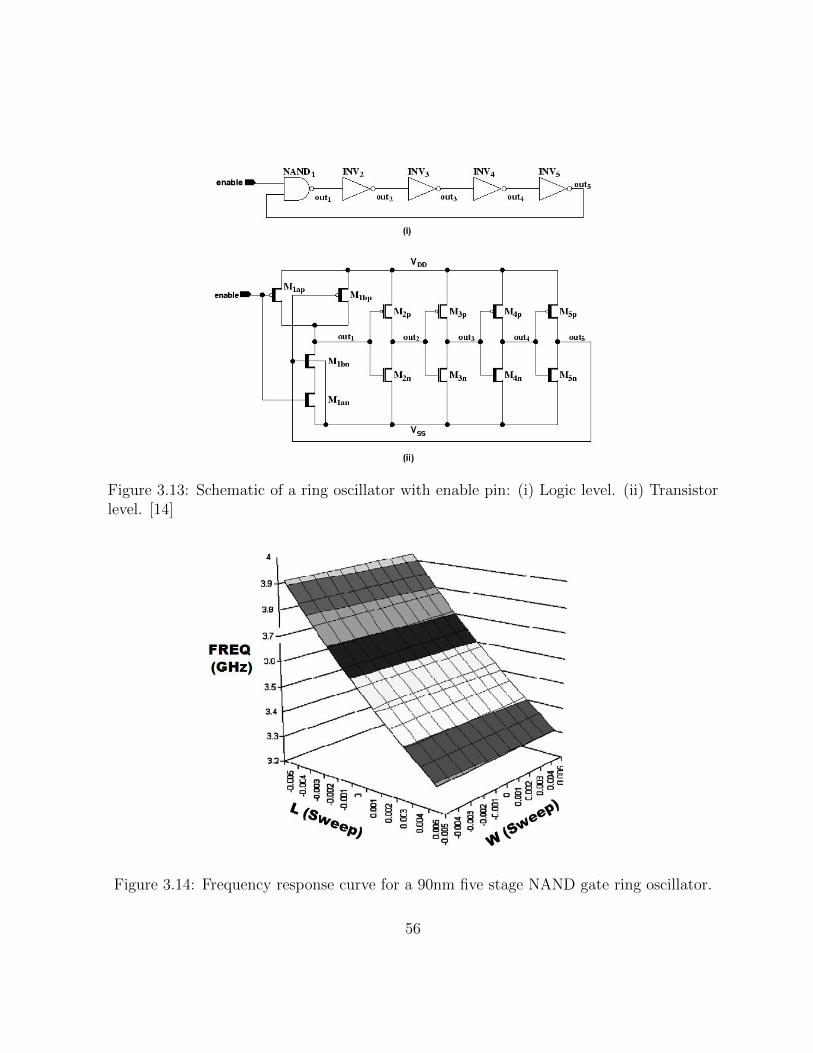
Figure 3.13: Schematic of a ring oscillator with enable pin: (i) Logic level. (ii) Transistorlevel. [14]
Figure 3.14: Frequency response curve for a 90nm five stage NAND gate ring oscillator.
56
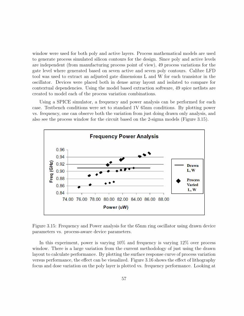
window were used for both poly and active layers. Process mathematical models are usedto generate process simulated silicon contours for the design. Since poly and active levelsare independent (from manufacturing process point of view), 49 process variations for thegate level where generated based on seven active and seven poly contours. Calibre LFDtool was used to extract an adjusted gate dimensions L and W for each transistor in theoscillator. Devices were placed both in dense array layout and isolated to compare forcontextual dependencies. Using the model based extraction software, 49 spice netlists arecreated to model each of the process variation combinations.
Using a SPICE simulator, a frequency and power analysis can be performed for eachcase. Testbench conditions were set to standard 1V 65nm conditions. By plotting powervs. frequency, one can observe both the variation from just doing drawn only analysis, andalso see the process window for the circuit based on the 2-sigma models (Figure 3.15).
Figure 3.15: Frequency and Power analysis for the 65nm ring oscillator using drawn deviceparameters vs. process-aware device parameters.
In this experiment, power is varying 10% and frequency is varying 12% over processwindow. There is a large variation from the current methodology of just using the drawnlayout to calculate performance. By plotting the surface response curve of process variationversus performance, the effect can be visualized. Figure 3.16 shows the effect of lithographyfocus and dose variation on the poly layer is plotted vs. frequency performance. Looking at
57
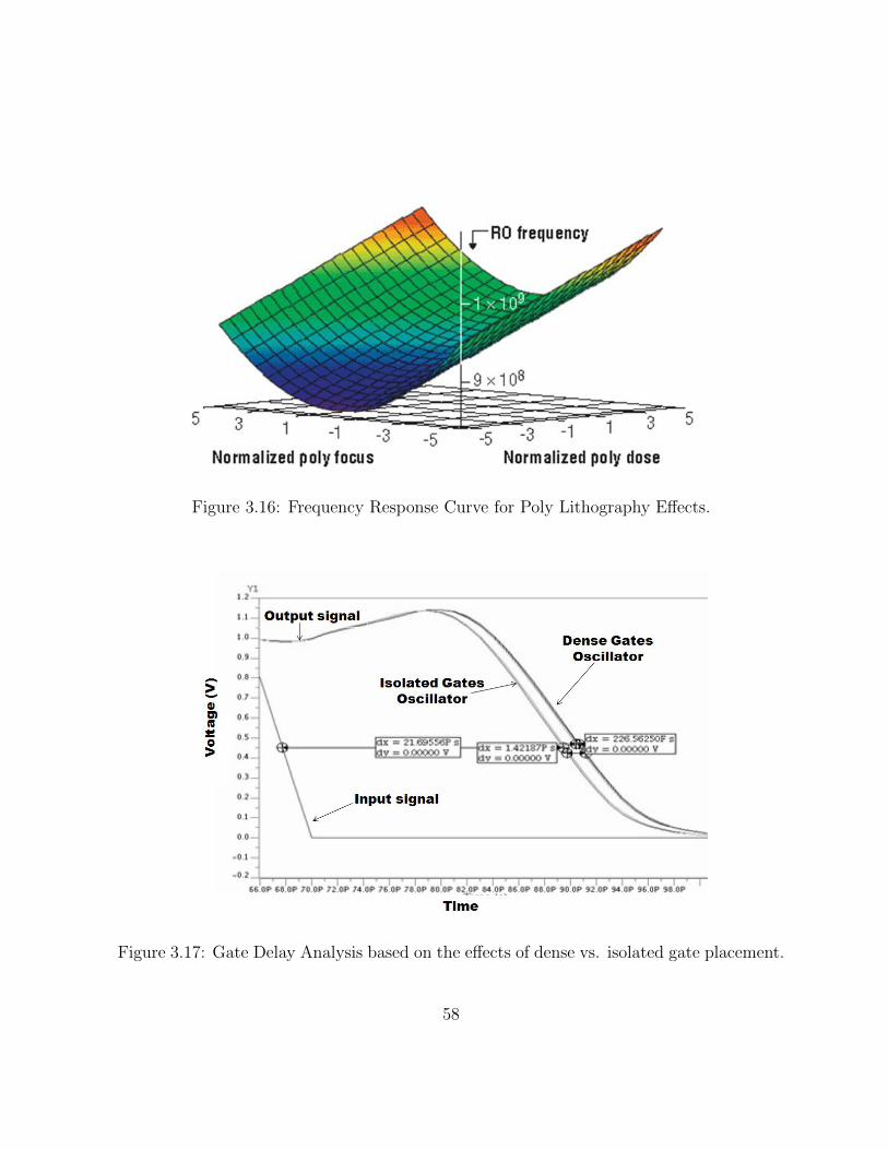
Figure 3.16: Frequency Response Curve for Poly Lithography Effects.
Figure 3.17: Gate Delay Analysis based on the effects of dense vs. isolated gate placement.
58

the amount of gate variation that is created at various process conditions vs. isolated anddense gate layout, one can calculate the timing differences in gate delay based on layoutcontext dependency (Figure 3.17).
3.6 Summary
Lithography and stress variations are two dominant effects impacting the functionality andperformance of designs at 65nm and below. In addition; proximity effects from neighboringcells, significantly influence the lithography process and stress variations values. Thereforestudying the design context has to be considered in any variability-aware circuit analysis.In understanding the accuracy demands of nanometer design simulation, there is a needto accurately characterize the process variations. It has been proved that characterizingthe standard cells in isolation and lack of awareness of the design context would lead to aninaccurate circuit analysis. This chapter proposed a methodology to characterize the designcontext impact on the process variations and hence on the cell’s electrical parameters. Themain contributions of the proposed methodology are listed as follows:
• Design context awareness: Context generator engine was implemented to simulatethe design context effect.
• Study the effects of different systematic variations such as lithography and stresseffects.
• A quantitative study of the impact of systematic variations for different circuits’electrical and geometrical behavior
The design context-aware process variations were examined on 65nm and 45nm indus-trial standard cell libraries and a 65nm five stage NAND ring oscillator. Results showedthat power and frequency depends on the systematic process variations.
59
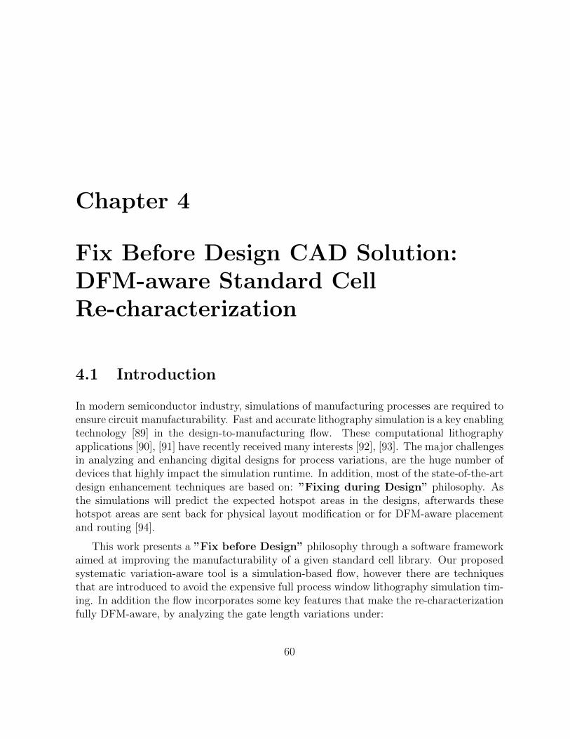
Chapter 4
Fix Before Design CAD Solution:DFM-aware Standard CellRe-characterization
4.1 Introduction
In modern semiconductor industry, simulations of manufacturing processes are required toensure circuit manufacturability. Fast and accurate lithography simulation is a key enablingtechnology [89] in the design-to-manufacturing flow. These computational lithographyapplications [90], [91] have recently received many interests [92], [93]. The major challengesin analyzing and enhancing digital designs for process variations, are the huge number ofdevices that highly impact the simulation runtime. In addition, most of the state-of-the-artdesign enhancement techniques are based on: ”Fixing during Design” philosophy. Asthe simulations will predict the expected hotspot areas in the designs, afterwards thesehotspot areas are sent back for physical layout modification or for DFM-aware placementand routing [94].
This work presents a ”Fix before Design” philosophy through a software frameworkaimed at improving the manufacturability of a given standard cell library. Our proposedsystematic variation-aware tool is a simulation-based flow, however there are techniquesthat are introduced to avoid the expensive full process window lithography simulation tim-ing. In addition the flow incorporates some key features that make the re-characterizationfully DFM-aware, by analyzing the gate length variations under:
60

• Different process conditions throughout the complete process window.
• Different design contexts using density based context variation.
• Different RET aggressiveness.
DFM metrics are extracted from this flow, such as the optimum placement locations ofstandard cells, which can guide the designer for a more robust and manufacture-awareplacement and routing design. This flow is verified by re-designing the critical paths of45nm Finite Impulse Response (FIR) filter circuit using the DFM-aware library.
4.2 Background
Recently, other solutions perform timing analysis to standard cells, such as [13] and [82],however the proposed fully automated methodology presented in this chapter, differs fromthe other work done such by the following:
1. As the lithographical simulations that include different process window conditions arecrucial for verification of designs for technology nodes of deep sub-wavelength criticaldimension, the runtime penalty of simulating at different process condition is large.Analytical methods that accounts for different lithographical simulation are limitedto few process window conditions such as dose, focus and overlay shift. New techniqueis used to filter redundant combination of process conditions, pick specific conditionsthat need to be passed to electrical extraction, and mark placements of cells that willresult in different lithographical simulation results. The suggested method namedIsolated Process Point Engine (IPPE) can account for any changing parameter thatneed to be considered in the process window simulations, and provide a systematicway to filter redundant process conditions through contours comparisons. Moreoverthis analysis is done once per technology and no need to re-run this engine for eachdesign. (IPPE) identifies the optimum and unique process conditions that repre-sent the total process variation. This engine helps to reduces computation time byavoiding the simulation of all possible process and lithography conditionsand instead use optimized number of process conditions that is proven torepresent the complete process window while not compromising the quality ofsimulation.
61
2. The proposed flow examines the effect of different Resolution Enhancement Tech-niques (RET) recipes on timing and power analysis. Since lithographic contoursare highly dependent on the RET techniques applied to a design [95], having theflexibility to examine different RET recipes is key for proper standard cell character-ization. Besides considering different RET aggressiveness into the re-characterizationflow, several new RET design concepts can be concluded from this feature as well,such as selective RET concept, where the RET engineer can define smartly the RETaggressiveness needed based on the type of the cell used and its location in the chip.
3. Several manufacturability aware metrics are proposed to be added to the standardcell library in a format that is understood by place and route tools. These metrics willbetter quantify the robustness of standard cell to layout context variations, and alsoguide the placement tool where would be the optimum location to place the standardcell. In addition a design-aware metric is also proposed for the RET engineers duringtheir post layout operations aiding them to smartly selective the proper and optimumRET aggressiveness for such design.
4.3 DFM-aware standard cell re-characterization flow
Figure 4.1 illustrates the proposed flow for litho-aware standard cells characterization [96],while figure 4.2 shows the pseudo code used to implement the flow. The first step inthis methodology,is placing the standard cells in different contexts using the density basedcontext generator engine. Secondly, RET is applied on these cells, with different aggres-siveness. In the third step, the lithography contours are simulated at a specific processcondition, to identify layout topologies that are sensitive to this process condition, knownas litho-hotspots. Lithography simulations are repeated at different process conditions tocover the complete lithography process variations. This step is done using CalibreTMLFDfor predicting the manufacturing variability through process variation. By accurately sim-ulating the different effects of the lithographic process this enables designers to maketrade-off decisions early, resulting in a design that is more robust and less sensitive tothe lithographic process window. Calibre LFD use a built-in function known as ProcessVariability bands (PV-bands) [97] [98]. To generate the PV-bands, all different processcorners conditions need to be fed to the simulator. However to simulate all expected pro-cess conditions, a major runtime issue will show up. To understand the issue, let us assumethe variation in the lithography process is caused by variation in the dose of the light thatvaries, for example, from 90% to 110% from its nominal value. To cover this range, steps of10 dose conditions are considered. Another source of lithography variation is the variation
62
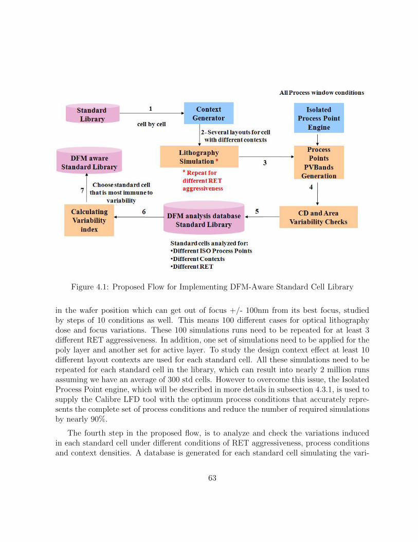
Figure 4.1: Proposed Flow for Implementing DFM-Aware Standard Cell Library
in the wafer position which can get out of focus +/- 100nm from its best focus, studiedby steps of 10 conditions as well. This means 100 different cases for optical lithographydose and focus variations. These 100 simulations runs need to be repeated for at least 3different RET aggressiveness. In addition, one set of simulations need to be applied for thepoly layer and another set for active layer. To study the design context effect at least 10different layout contexts are used for each standard cell. All these simulations need to berepeated for each standard cell in the library, which can result into nearly 2 million runsassuming we have an average of 300 std cells. However to overcome this issue, the IsolatedProcess Point engine, which will be described in more details in subsection 4.3.1, is used tosupply the Calibre LFD tool with the optimum process conditions that accurately repre-sents the complete set of process conditions and reduce the number of required simulationsby nearly 90%.
The fourth step in the proposed flow, is to analyze and check the variations inducedin each standard cell under different conditions of RET aggressiveness, process conditionsand context densities. A database is generated for each standard cell simulating the vari-
63
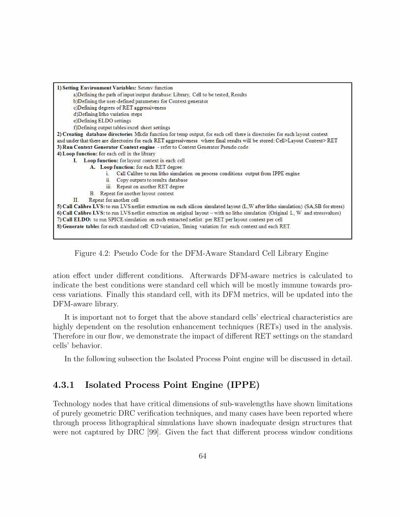
Figure 4.2: Pseudo Code for the DFM-Aware Standard Cell Library Engine
ation effect under different conditions. Afterwards DFM-aware metrics is calculated toindicate the best conditions were standard cell which will be mostly immune towards pro-cess variations. Finally this standard cell, with its DFM metrics, will be updated into theDFM-aware library.
It is important not to forget that the above standard cells’ electrical characteristics arehighly dependent on the resolution enhancement techniques (RETs) used in the analysis.Therefore in our flow, we demonstrate the impact of different RET settings on the standardcells’ behavior.
In the following subsection the Isolated Process Point engine will be discussed in detail.
4.3.1 Isolated Process Point Engine (IPPE)
Technology nodes that have critical dimensions of sub-wavelengths have shown limitationsof purely geometric DRC verification techniques, and many cases have been reported wherethrough process lithographical simulations have shown inadequate design structures thatwere not captured by DRC [99]. Given the fact that different process window conditions
64
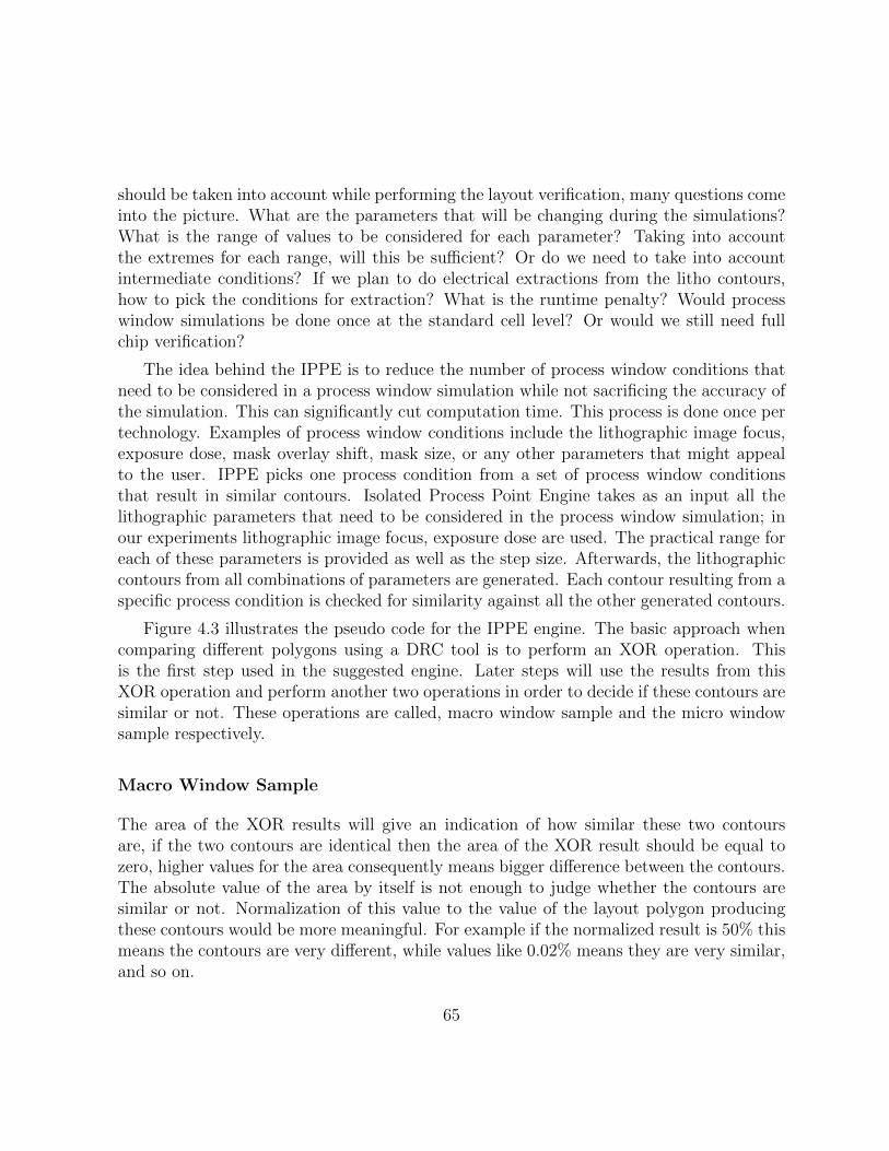
should be taken into account while performing the layout verification, many questions comeinto the picture. What are the parameters that will be changing during the simulations?What is the range of values to be considered for each parameter? Taking into accountthe extremes for each range, will this be sufficient? Or do we need to take into accountintermediate conditions? If we plan to do electrical extractions from the litho contours,how to pick the conditions for extraction? What is the runtime penalty? Would processwindow simulations be done once at the standard cell level? Or would we still need fullchip verification?
The idea behind the IPPE is to reduce the number of process window conditions thatneed to be considered in a process window simulation while not sacrificing the accuracy ofthe simulation. This can significantly cut computation time. This process is done once pertechnology. Examples of process window conditions include the lithographic image focus,exposure dose, mask overlay shift, mask size, or any other parameters that might appealto the user. IPPE picks one process condition from a set of process window conditionsthat result in similar contours. Isolated Process Point Engine takes as an input all thelithographic parameters that need to be considered in the process window simulation; inour experiments lithographic image focus, exposure dose are used. The practical range foreach of these parameters is provided as well as the step size. Afterwards, the lithographiccontours from all combinations of parameters are generated. Each contour resulting from aspecific process condition is checked for similarity against all the other generated contours.
Figure 4.3 illustrates the pseudo code for the IPPE engine. The basic approach whencomparing different polygons using a DRC tool is to perform an XOR operation. Thisis the first step used in the suggested engine. Later steps will use the results from thisXOR operation and perform another two operations in order to decide if these contours aresimilar or not. These operations are called, macro window sample and the micro windowsample respectively.
Macro Window Sample
The area of the XOR results will give an indication of how similar these two contoursare, if the two contours are identical then the area of the XOR result should be equal tozero, higher values for the area consequently means bigger difference between the contours.The absolute value of the area by itself is not enough to judge whether the contours aresimilar or not. Normalization of this value to the value of the layout polygon producingthese contours would be more meaningful. For example if the normalized result is 50% thismeans the contours are very different, while values like 0.02% means they are very similar,and so on.
65
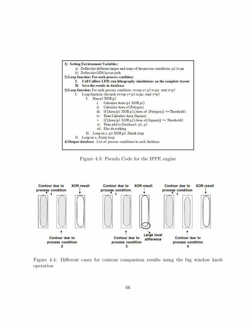
Figure 4.3: Pseudo Code for the IPPE engine
Figure 4.4: Different cases for contour comparison results using the big window knoboperation
66

This operation will catch the general similarity between the two contours under inves-tigation, however some case might be encountered where the value of the macro windowsample is small, but there are some high local area differences. To deal with local differencesthe micro window sample operation is used.
Figure 4.4 shows three different cases for XOR of different contours. Case 1 is the leftmost picture where the contours are nearly identical and the XOR area is very small, Case2 is the middle picture that shows low value for the macro window sample but there existsa local high difference between the contours that is not captured by this operation, Case3 is the right most picture that shows high value for the macro window sample and twodifferent contours.
However, the macro window operation by itself is not sufficient to decide if the contoursare similar or not. There can be a situation where two contours have only one large localdifference, but not large enough to exceed the pre-defined threshold, causing the contoursto be treated similar. Therefore the macro window operation is followed by a micro windowoperation.
Micro Window Sample
The micro sample operation is a scanning operation. A small square of few nano metersside length is swept over the XOR result from the two contours under test, the area of theXOR result inside the square is reported for different locations as the scanning progresses.If there is a location where the value of the area of the XOR result is larger than a giventhreshold, then this means there is a local difference at this spot, and the contours cannot be considered similar. Figure 4.5 shows the small scanning window, the window runsover the XOR results in all directions, the area of the XOR result is checked every timethe square steps in positions.
The micro window operation by itself is not sufficient to decide if the contours aresimilar or not. There can be a situation where the area inside the scanning square isalways less than threshold but when all areas are summed, the overall difference is largeenough to consider the contours different.
The complete flow for comparing the similarity between to process conditions is shownin figure 4.6.
Having a systematic methodology for deciding if two contours are similar or not, we canreduce the number of process window conditions that need to be considered in a processwindow simulation by picking one process window condition from a set of process window
67
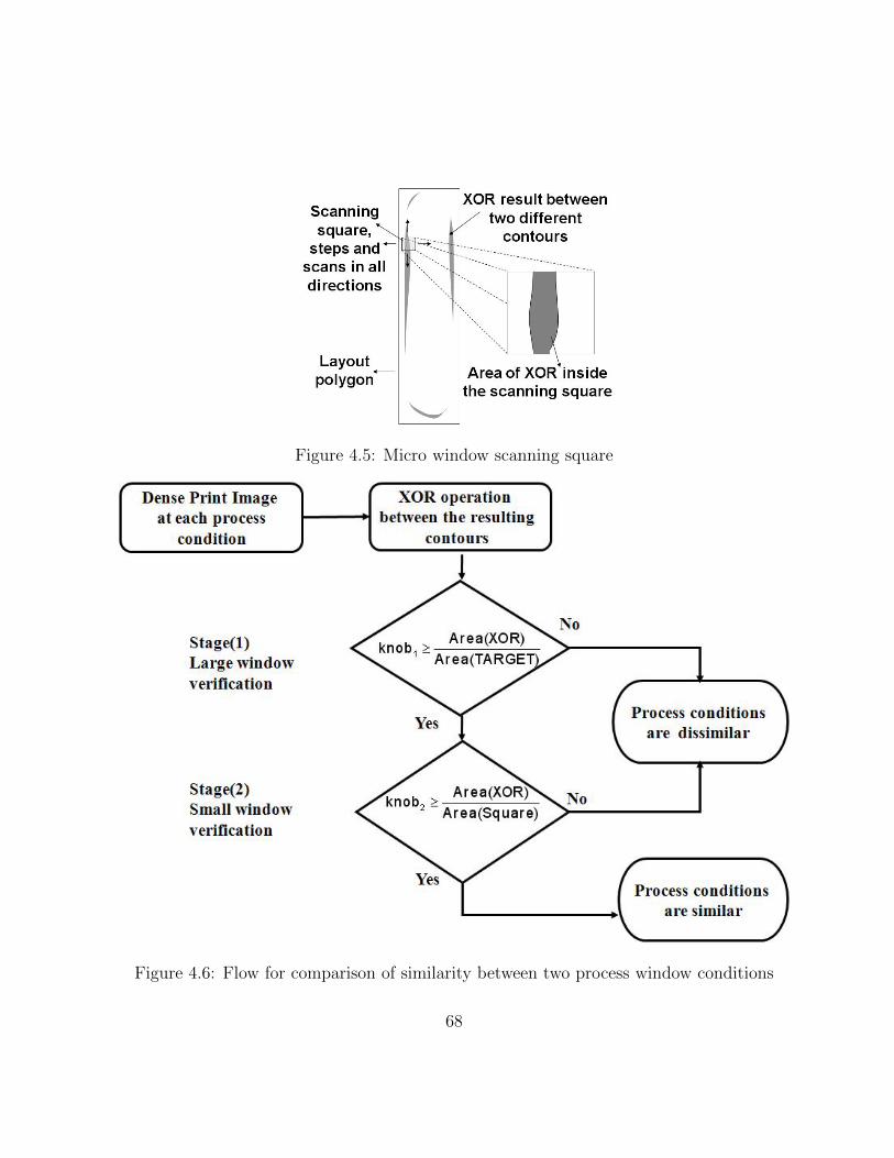
Figure 4.5: Micro window scanning square
Figure 4.6: Flow for comparison of similarity between two process window conditions
68
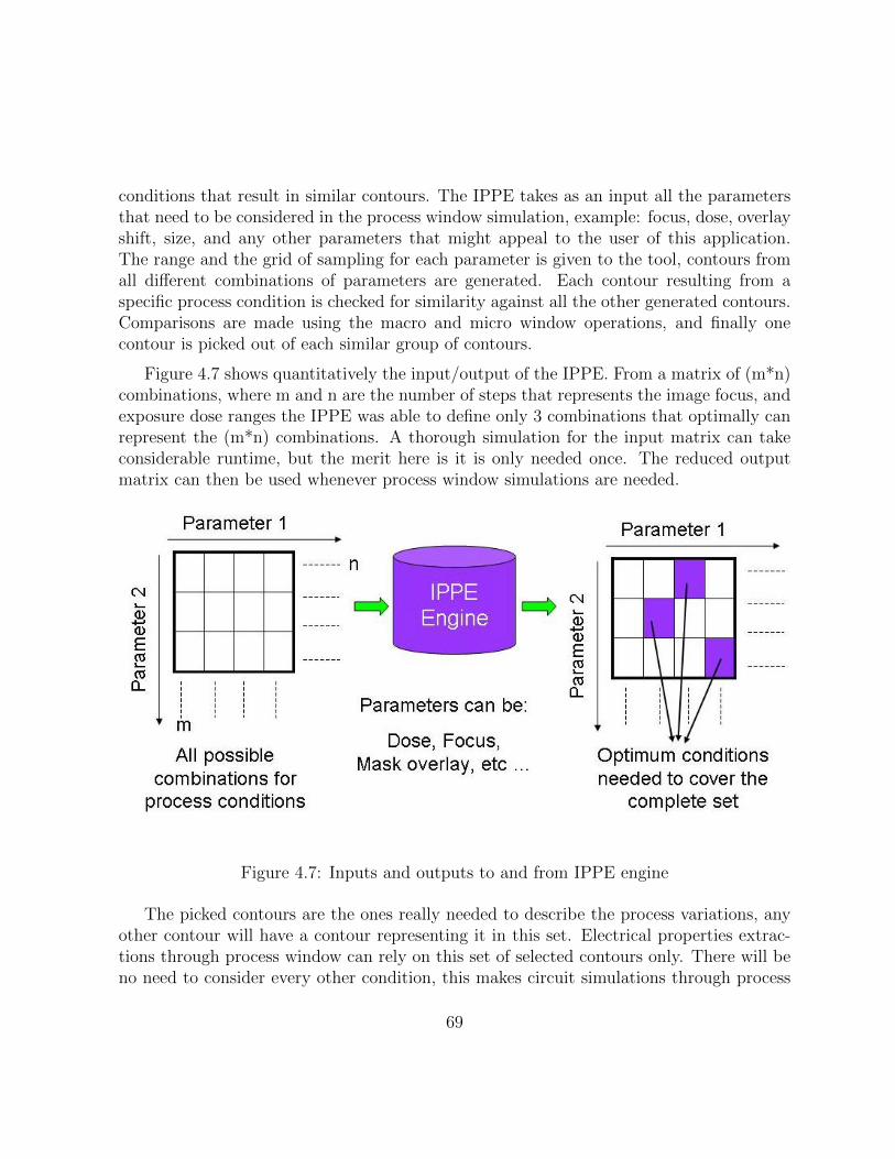
conditions that result in similar contours. The IPPE takes as an input all the parametersthat need to be considered in the process window simulation, example: focus, dose, overlayshift, size, and any other parameters that might appeal to the user of this application.The range and the grid of sampling for each parameter is given to the tool, contours fromall different combinations of parameters are generated. Each contour resulting from aspecific process condition is checked for similarity against all the other generated contours.Comparisons are made using the macro and micro window operations, and finally onecontour is picked out of each similar group of contours.
Figure 4.7 shows quantitatively the input/output of the IPPE. From a matrix of (m*n)combinations, where m and n are the number of steps that represents the image focus, andexposure dose ranges the IPPE was able to define only 3 combinations that optimally canrepresent the (m*n) combinations. A thorough simulation for the input matrix can takeconsiderable runtime, but the merit here is it is only needed once. The reduced outputmatrix can then be used whenever process window simulations are needed.
Figure 4.7: Inputs and outputs to and from IPPE engine
The picked contours are the ones really needed to describe the process variations, anyother contour will have a contour representing it in this set. Electrical properties extrac-tions through process window can rely on this set of selected contours only. There will beno need to consider every other condition, this makes circuit simulations through process
69
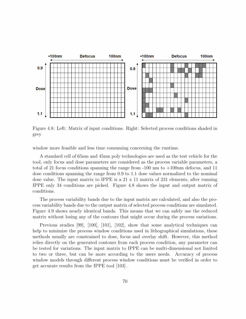
Figure 4.8: Left: Matrix of input conditions. Right: Selected process conditions shaded ingrey
window more feasible and less time consuming concerning the runtime.
A standard cell of 65nm and 45nm poly technologies are used as the test vehicle for thetool, only focus and dose parameters are considered as the process variable parameters, atotal of 21 focus conditions spanning the range from -100 nm to +100nm defocus, and 11dose conditions spanning the range from 0.9 to 1.1 dose values normalized to the nominaldose value. The input matrix to IPPE is a 21 x 11 matrix of 231 elements, after runningIPPE only 34 conditions are picked. Figure 4.8 shows the input and output matrix ofconditions.
The process variability bands due to the input matrix are calculated, and also the pro-cess variability bands due to the output matrix of selected process conditions are simulated.Figure 4.9 shows nearly identical bands. This means that we can safely use the reducedmatrix without losing any of the contours that might occur during the process variations.
Previous studies [99], [100], [101], [102], show that some analytical techniques canhelp to minimize the process window conditions used in lithographical simulations, thesemethods usually are constrained to dose, focus and overlay shift. However, this methodrelies directly on the generated contours from each process condition, any parameter canbe tested for variations. The input matrix to IPPE can be multi-dimensional not limitedto two or three, but can be more according to the users needs. Accuracy of processwindow models through different process window conditions must be verified in order toget accurate results from the IPPE tool [103] .
70
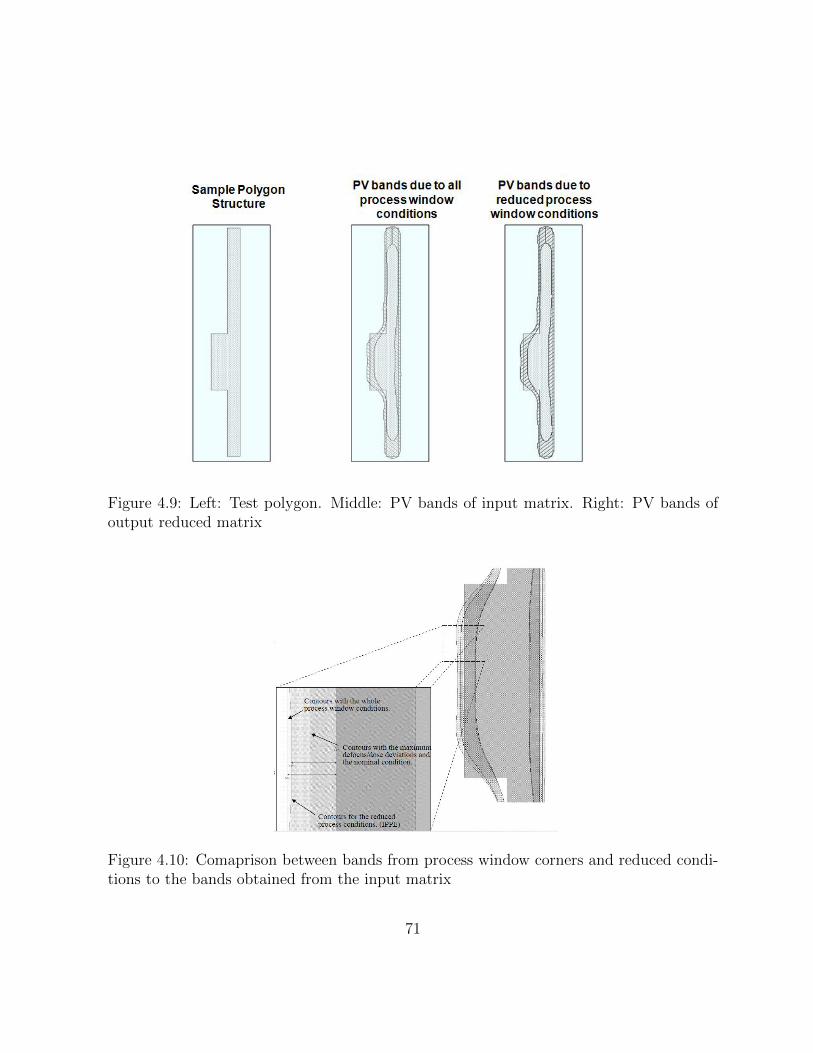
Figure 4.9: Left: Test polygon. Middle: PV bands of input matrix. Right: PV bands ofoutput reduced matrix
Figure 4.10: Comaprison between bands from process window corners and reduced condi-tions to the bands obtained from the input matrix
71
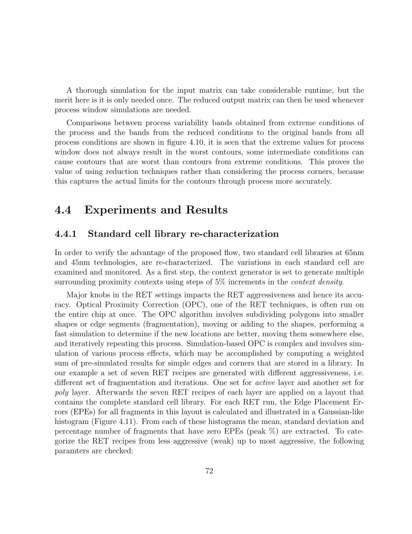
A thorough simulation for the input matrix can take considerable runtime, but themerit here is it is only needed once. The reduced output matrix can then be used wheneverprocess window simulations are needed.
Comparisons between process variability bands obtained from extreme conditions ofthe process and the bands from the reduced conditions to the original bands from allprocess conditions are shown in figure 4.10, it is seen that the extreme values for processwindow does not always result in the worst contours, some intermediate conditions cancause contours that are worst than contours from extreme conditions. This proves thevalue of using reduction techniques rather than considering the process corners, becausethis captures the actual limits for the contours through process more accurately.
4.4 Experiments and Results
4.4.1 Standard cell library re-characterization
In order to verify the advantage of the proposed flow, two standard cell libraries at 65nmand 45nm technologies, are re-characterized. The variations in each standard cell areexamined and monitored. As a first step, the context generator is set to generate multiplesurrounding proximity contexts using steps of 5% increments in the context density.
Major knobs in the RET settings impacts the RET aggressiveness and hence its accu-racy. Optical Proximity Correction (OPC), one of the RET techniques, is often run onthe entire chip at once. The OPC algorithm involves subdividing polygons into smallershapes or edge segments (fragmentation), moving or adding to the shapes, performing afast simulation to determine if the new locations are better, moving them somewhere else,and iteratively repeating this process. Simulation-based OPC is complex and involves sim-ulation of various process effects, which may be accomplished by computing a weightedsum of pre-simulated results for simple edges and corners that are stored in a library. Inour example a set of seven RET recipes are generated with different aggressiveness, i.e.different set of fragmentation and iterations. One set for active layer and another set forpoly layer. Afterwards the seven RET recipes of each layer are applied on a layout thatcontains the complete standard cell library. For each RET run, the Edge Placement Er-rors (EPEs) for all fragments in this layout is calculated and illustrated in a Gaussian-likehistogram (Figure 4.11). From each of these histograms the mean, standard deviation andpercentage number of fragments that have zero EPEs (peak %) are extracted. To cate-gorize the RET recipes from less aggressive (weak) up to most aggressive, the followingparamters are checked:
72
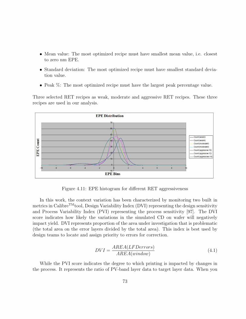
• Mean value: The most optimized recipe must have smallest mean value, i.e. closestto zero nm EPE.
• Standard deviation: The most optimized recipe must have smallest standard devia-tion value.
• Peak %: The most optimized recipe must have the largest peak percentage value.
Three selected RET recipes as weak, moderate and aggressive RET recipes. These threerecipes are used in our analysis.
Figure 4.11: EPE histogram for different RET aggressiveness
In this work, the context variation has been characterized by monitoring two built inmetrics in CalibreTMtool, Design Variability Index (DVI) representing the design sensitivityand Process Variability Index (PVI) representing the process sensitivity [97]. The DVIscore indicates how likely the variations in the simulated CD on wafer will negativelyimpact yield. DVI represents proportion of the area under investigation that is problematic(the total area on the error layers divided by the total area). This index is best used bydesign teams to locate and assign priority to errors for correction.
DV I =AREA(LFDerrors)
AREA(window)(4.1)
While the PVI score indicates the degree to which printing is impacted by changes inthe process. It represents the ratio of PV-band layer data to target layer data. When you
73

perform multiple process variation experiments on the same layer, all the experiments arefactored into the scores.
PV I =AREA(pvband(layer))
AREA(layer)(4.2)
After calculating the CD Variations, PVI and DVI values for a standard cell underdifferent contexts and RET aggressiveness, two proposed metrics are extracted: ContextSafety Zone (CSZ) and Context Robustness (CR). CSZ is defined as the maximum accept-able context variation, depicted and described as follows:
CSZ = Density at the maximum of (PV Iminimum + σPV I) or (DV Iminimum + σDV I)
where σ is the standard deviation of the process and design variations under all possiblecontext densities.
The context safety zone is a useful metric that can guide the way a circuit is synthesizedand/or place and routed. At the synthesis phase, a library of standard cells is placed incontext that is considered immune to variability. Figures 4.12 and 4.13 represents theprocess variations in the AOI topology under different contexts. In this example, thePVI standard deviation under all possible context densities was equal to 2.1 and for DVIstandard deviation equal to 0.75. It can be seen, in Figures 4.12 and 4.13, that this AOItopology will experience high process variations on the transistors dimensions when usedin less dense areas <55%, while this AOI will be nearly immune to process variations whenits context has an Context Density >55%. It is worth mentioning that the standard cellsused in our test case had dummy poly similar to what was recommended in [82], confirmingthat the impact of manufacturing variations on devices is layout context dependent.
Another metric we defined in our methodology is the Context Robustness (CR). CRis a statistical parameter that represents the robustness of a cell to the context variation(defined using equation 4.3) . This metric is useful to give the designer an indication howthe standard cells are immune to context variation under different RETs conditions.
CR =(Mean− CV )
Mean(4.3)
where the mean is the average value of DVI through context variations and the coeffi-cient of variation (CV) is defined as the ratio of the standard deviation to the mean . CR
74
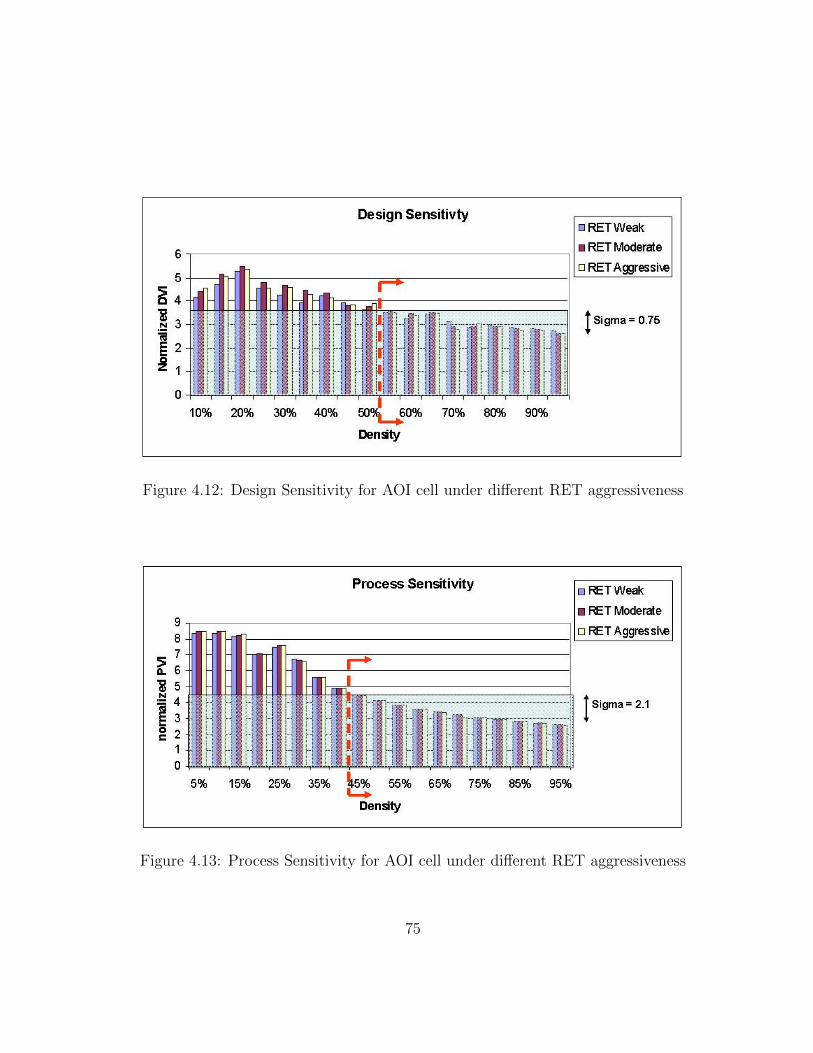
Figure 4.12: Design Sensitivity for AOI cell under different RET aggressiveness
Figure 4.13: Process Sensitivity for AOI cell under different RET aggressiveness
75
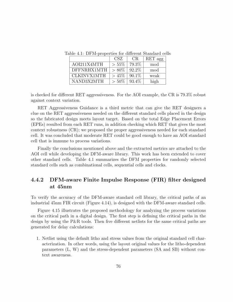
Table 4.1: DFM-properties for different Standard cellsCSZ CR RET agg
AOI211X4MTH > 55% 79.3% modDFFNRHX1MTH > 80% 92.2% modCLKINVX1MTH > 45% 90.1% weakNAND3X2MTH > 50% 93.4% high
is checked for different RET aggressiveness. For the AOI example, the CR is 79.3% robustagainst context variation.
RET Aggressiveness Guidance is a third metric that can give the RET designers aclue on the RET aggressiveness needed on the different standard cells placed in the designso the fabricated design meets layout target. Based on the total Edge Placement Errors(EPEs) resulted from each RET runs, in addition checking which RET that gives the mostcontext robustness (CR); we proposed the proper aggressiveness needed for each standardcell. It was concluded that moderate RET could be good enough to have an AOI standardcell that is immune to process variations.
Finally the conclusions mentioned above and the extracted metrics are attached to theAOI cell while developing the DFM-aware library. This work has been extended to coverother standard cells. Table 4.1 summarizes the DFM properties for randomly selectedstandard cells such as combinational cells, sequential cells and clocks.
4.4.2 DFM-aware Finite Impulse Response (FIR) filter designedat 45nm
To verify the accuracy of the DFM-aware standard cell library, the critical paths of anindustrial 45nm FIR circuit (Figure 4.14), is designed with the DFM-aware standard cells.
Figure 4.15 illustrates the proposed methodology for analyzing the process variationson the critical path in a digital design. The first step is defining the critical paths in thedesign by using the P&R tools. Then five different netlists for the same critical paths aregenerated for delay calculations:
1. Netlist using the default litho and stress values from the original standard cell char-acterization. In other words, using the layout original values for the litho-dependentparameters (L, W) and the stress-dependent parameters (SA and SB) without con-text awareness.
76
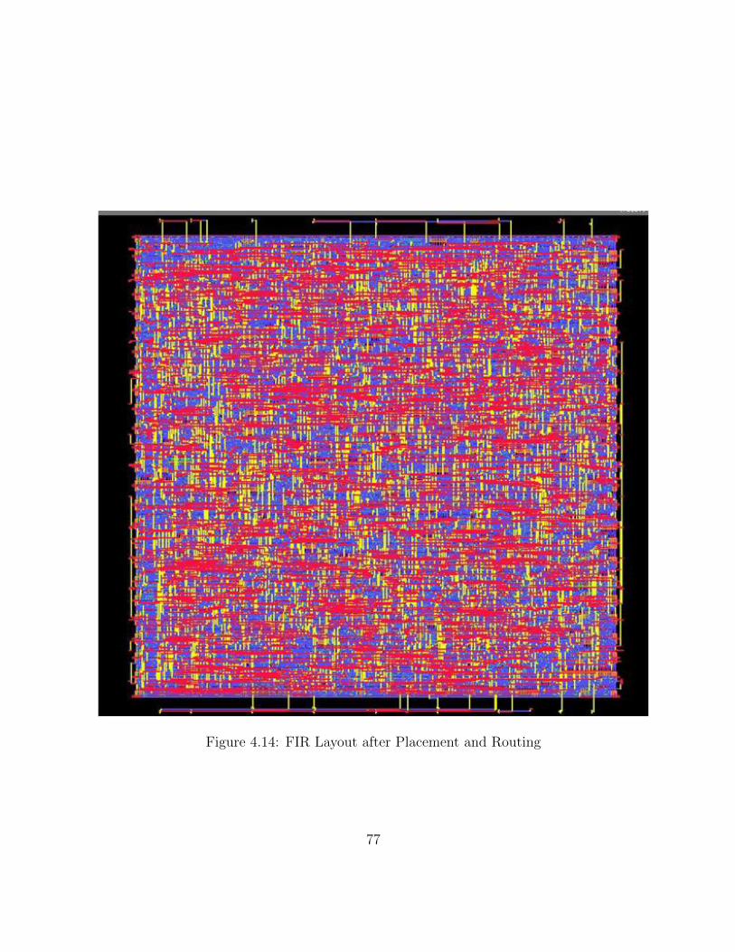
Figure 4.14: FIR Layout after Placement and Routing
77

2. Netlist using DFM-aware standard cells that were only characterized for lithographyeffects. This netlist is used only for analysis purpose.
3. Netlist using DFM-aware standard cells that were only characterized for stress effects.This netlist is used only for analysis purpose.
4. Netlist using DFM-aware standard cells that were characterized for lithography andstress effects.
5. Netlist using the extracted litho and stress parameters from the actual and full FIRlayout using silicon simulation (Figure 4.16). For each standard cell in the criticalpath, the design-aware stress parameters such as the SA and SB parameters areextracted. In other words, the transistor stress parameters are re-evaluated by takinginto account the real design context, instead of the parameters that are pre-definedin the standard cell netlist. These proximity parameters are extracted by LVS andupdated in each standard cell transistor level netlist. Regarding the lithographyeffects, an industrial design kit containing look up tables for the equivalent L and Wvalues according to their context, is used instead of full chip lithography simulation.
Table 4.2: Timing reports simulating standard netlist versus process-aware netlists
Path 1 (ps) Path 2 (ps)
Netlist 1 3368.834 3509.546Netlist 2 3361.22 3491.88Netlist 3 3100.966 3293.622Netlist 4 3082.414 3256.776Netlist 5 3035.22 3204.632
Table 4.2 lists the path delay calculated by different netlists. Several interesting obser-vations can be drawn from our study:
1. Context awareness characterization is necessary: There is nearly a deviationof 250-300 ps, equivalent to 10% error in timing calculations, between the delaysimulated using context-aware netlists (Netlists 2,3,4,5) versus delays calculated fromNetlist 1, where litho and stress dependent parameters characterized without contextinformation.
78
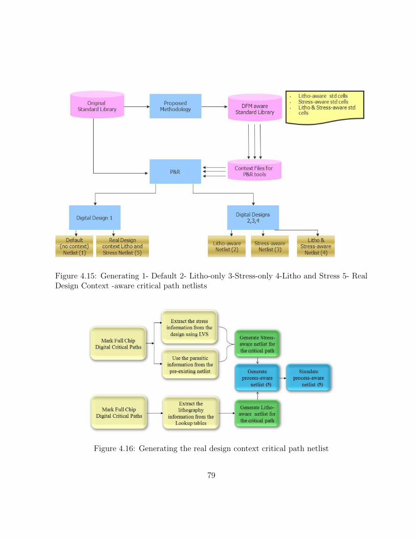
Figure 4.15: Generating 1- Default 2- Litho-only 3-Stress-only 4-Litho and Stress 5- RealDesign Context -aware critical path netlists
Figure 4.16: Generating the real design context critical path netlist
79

2. Accuracy of the DFM tool: Comparing Netlist 4 with Netlist 5, indicates thatthe characterization of the standard cells using the proposed solution gives a goodpredication of real design context (around 1% error in timing calculations).
3. Lithography vs. Stress: Comparing Netlist 2 with Netlist 3, indicates that lithog-raphy effects contribute to the timing variations in a less matter than stress effects.However this can not be a general conclusion to any other designs.
4. Qualifying the Standard Cell Library: Even though an industrial standard celllibrary is used in these experiments, it is worth mentioning that using a 45nm opensource standard cell library where context awareness characterization was not per-formed during library characterization, can substantially impact the results. TheFreePDK45 design kit [104] shows that the delay response due to the lithographyvariations only exhibits a behavior with a variation as high as 20ps per cell. It isevident that the timing variation is highly dependent on the characterization method-ology. This conclusion supports the importance of implementing a DFM-aware stan-dard cell library and using the updated library in the P&R. Lately, the high-techindustrial foundries have recognized the importance of DFM-aware standard cell re-characterization, and they started to characterize their advanced node standard celllibraries taking into considerations the lithography, stress and context impact.
4.5 Summary
In understanding the accuracy demands of nanometer design simulation, there is a need toadd the capability of using silicon simulation based DFM solution to calculate standard cellcharacteristics. In this chapter we introduced a Fix before Design software frameworkaimed at improving the manufacturability of a given standard cell library. The maincontributions of the proposed CAD solution are listed as follows:
• Reduce the design development cycles and the multiple design respins that arisefrom other ”Fixing during Design” DFM solutions by providing a robust designs fromthe first design cycles.
• The proposed CAD solution re-characterizes the standard cell under different de-sign contexts and Resolution Enhancement Techniques (RET).
• Dramatically reduce the lithography simulation runtime by introducing anovel engine that intelligently groups similar lithography effects within different pro-cess conditions.
80

To validate this work, we have re-designed the critical paths of FIR filter circuit usingthe DFM-aware library. An error of 1% was the difference when comparing the timing ofthe critical paths using full silicon simulations versus the critical paths designed from theDFM-aware library.
81

Chapter 5
High Performance Electrical DrivenHotspot Detection CAD Solution forFull Chip Design using a NovelDevice Parameter MatchingTechnique
5.1 Introduction
With the continuous development of today’s technology, IC design becomes a more complexprocess. The designer now not only takes care of the normal design and layout parametersas usual, but also needs to consider the process variation impact on the design to preservethe same chip functionality with no failure during fabrication. In the current process,schematic designers go through extensive simulations to cover all the possible variations oftheir design parameters and hence of the design functionality. At the same time, layoutdesigners perform time-consuming process-aware simulations (such as lithography simula-tions) on the full chip layout, which impacts the design turn-around time. In this chapter,we present a fast physical and electrical-aware Design-For-Manufacturability (DFM) solu-tion that detects hotspot areas in the full chip design without requiring extensive electricaland process simulations. Novel algorithms are proposed to implement the engines that areused to develop this solution. Our proposed flow is examined on a 45 nm industrial FiniteImpulse Response (FIR) full chip filter. The proposed methodology is able to define a list
82

of electrical hotspot devices located on the FIR critical path that experience up to 17%variation in their DC current values due to the effect of process and design context. Thetotal runtime needed to identify and detect these electrical hotspots on the full chip takesonly minutes, compared to hours and days when using conventional electrical and processsimulations.
The rest of this chapter is organized as follows: State-of-the-art hotspot detectionsolutions and their limitations are discussed in section 5.2. Section 5.3 depicts the proposedflow and algorithms entailed in implementing the engines used in the flow. To verify itsusefulness, the proposed methodology is examined on a FIR filter, and the results arehighlighted in Section 5.4. Finally, our concluding remarks are given in Section 5.5.
5.2 Background
As technology migrates from 90nm down to 45nm, it is increasingly difficult to achievefast yield ramp due to random defects, process variations, systematic yield problems, andother limitations referred to as design for manufacturing (DFM) issues. At 90nm andbelow, these problems often appear as layout hotspots. To avoid downstream yield andmanufacturing problems relating to layout hotspots, it is imperative that hotspots areaddressed by different DFM techniques, as will be discussed shortly. Successful DFMtechniques ensure high fabrication yield by incorporating manufacturability-aware modelsinto the design stage to identify and remove potentially problematic process hotspots.
5.2.1 Rule-based Hotspot Detection
Hotspots have to be detected before they can be corrected. Typically, fabs use designrules to represent hotspots [105], however, this representation is inadequate. Some manu-facturability issues are not local, for instance, lithography effects involve interactions overlonger distances than typical minimum spacing rules. Complex conditional rules and rec-ommended rules have been added to compensate some of this inadequacy; however, entirelyusing design rules for hotspot representation is resulting in an explosion of the design rulelibrary.
83

5.2.2 Model/Simulation-based Hotspot Detection
To address the limitations of design rules some process models have been incorporatedto analyze and drive corrections during the design stage. For instance, some design flowsinclude a full chip simulator to verify the design and identify potential hotspots [106], [107],[108]. However, these approaches have two major limitations [105]:
1. Lack of knowledge of downstream steps. It is impossible to accurately model certaindownstream processing steps such as OPC recipes. On the other hand, simple aerialimage-based lithography simulations often tag regions that can be easily correctedusing mask synthesis techniques. This over-estimation of hotspots is wasteful andcan produce an unnecessary burden on the designers.
2. Computational burden. Certain process models are computationally expensive andhard to incorporate during physical design.
A currently prevailing approach to detect hotspots is to predict the resist pattern byapplying a rigorous full chip post-OPC simulation and customer-defined checks [109], [110].It is flagged as a hotspot if a certain configuration does not pass the checks, and the de-tected hotspots are corrected accordingly. A full chip simulation is usually computationallyextensive, thus increasing the design-to-production time.
5.2.3 Pattern Matching-based Hotspot Detection
A pattern matching methodology has been developed to locate hotspots by scanning alayout using sample hotspots [111]. Pattern Matching is another approach that allowsdesign, manufacturing, and failure analysis teams to identify, isolate, and define specificgeometric configurations (patterns) directly from a design layout. Once recognized anddefined, these patterns can be added to a pattern library that can be used by differentpattern matching engines to automatically scan designs for matching patterns. Patternmatching itself is a very fast and efficient tool to identify hotspots, however, the populationof sample hotspots is usually huge if they directly come from an off-line full chip post-OPCsimulation. Therefore it is preferable if all the sample hotspots can be classified into groupsand the representative hotspot of each group is then used for pattern matching. Thus whenall the hotspots have been located, they are already classified into groups. Hotspots foundin one trial of pattern matching belong to the same class as the sample hotspot used forthis pattern matching trial. Furthermore, if a fixing solution is developed for the sample
84

hotspot, it can likely be applied to most of other hotspots in the same class. However suchtechniques experience from the following two major drawbacks:
1. Accuracy vs. Runtime tradeoff. The accuracy of the pattern matching techniquedepends on the quality of the pattern library (i.e. the number of patterns identifiedand added into the library). On the other hand too many patterns will lead to highover-estimate rate, and will directly increase the runtime of the flow and more falsealarm rate.
2. Purely geometrical-based. Today, many of the hotspot detection approachesthat use pattern matching techniques identify critical areas in the chip that areespecially susceptible to defects. Additionally, they identify the proximity effectscaused by the lithography process. However, these pattern matching tools are purely”geometric,” without any knowledge of the electrical characteristics of the shapesthat are manufactured in silicon [112]. Even other methods that incorporate moderndata mining and machine learning methods [113] into hotspot detection tasks stilldeal with hotspots as purely geometric.
5.2.4 Electrical-driven Hotspot Detection
While the previous techniques may be useful in identifying/fixing functional failures, andincreasing overall yield by a few percentage points, they completely ignore the more im-portant category of parametric failures. At 130nm and above, parametric failures are neg-ligible compared to functional failures. At 90nm, they become significant, and at 65nm,parametric failures become the single most critical yield-limiting factor [114] [115].
Electrical-driven DFM solutions have been proposed [95], [116] and [117] showing fairresults and good performance, however these solutions were directed to reduce only lithog-raphy variations by proposing performance-driven Optical Proximity Correction (OPC)solutions and standard cell re-characterization.
In this solution, a novel electrically-aware device parameter-based matching techniqueis proposed for hotspot detection. The device parameters represented in the SPICE modelscontain different abstracts of information, such as the layout geometry, the design contextand proximity effect on process variation, and the electrical information (Figure 5.1). Ourtechnique enables an electrically and manufacturability-aware solution that tackles para-metric yield issues. The fast and fully automated proposed CAD flow incorporates somekey features, as follows:
85
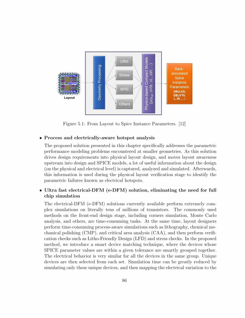
Figure 5.1: From Layout to Spice Instance Parameters. [12]
• Process and electrically-aware hotspot analysis
The proposed solution presented in this chapter specifically addresses the parametricperformance modeling problems encountered at smaller geometries. As this solutiondrives design requirements into physical layout design, and moves layout awarenessupstream into design and SPICE models, a lot of useful information about the design(on the physical and electrical level) is captured, analyzed and simulated. Afterwards,this information is used during the physical layout verification stage to identify theparametric failures known as electrical hotspots.
• Ultra fast electrical-DFM (e-DFM) solution, eliminating the need for fullchip simulation
The electrical-DFM (e-DFM) solutions currently available perform extremely com-plex simulations on literally tens of millions of transistors. The commonly usedmethods on the front-end design stage, including corners simulation, Monte Carloanalysis, and others, are time-consuming tasks. At the same time, layout designersperform time-consuming process-aware simulations such as lithography, chemical me-chanical polishing (CMP), and critical area analysis (CAA), and then perform verifi-cation checks such as Litho-Friendly Design (LFD) and stress checks. In the proposedmethod, we introduce a smart device matching technique, where the devices whoseSPICE parameter values are within a given tolerance are smartly grouped together.The electrical behavior is very similar for all the devices in the same group. Uniquedevices are then selected from each set. Simulation time can be greatly reduced bysimulating only these unique devices, and then mapping the electrical variation to the
86

rest of the devices in same group. At the same time, the process-aware simulationsthat are usually performed on the full chip layout are instead performed on areaswhere the devices that are considered critical or sensitive to variations are located.
• Automated intent driven design solution
Few standard practices have been established among designers, especially regardingcommunication of the design’s intent to those who layout the chip [118]. This is truefrom company to company, but also between design groups within the same orga-nization. Existing methods, such as placement of text notes on schematics, manualannotation of schematic printouts, and even verbal instruction, have proven to beinadequate. Improving this communication avoids major layout rework that addssignificant time to the design cycle. Important design requirements that are essen-tial for parametric performing silicon must be properly captured and communicatedto the layout designers. In the proposed flow, we present a fully automated enginethat not only captures electrical variation constraints resulting from the physical andparametric yield analysis (such as current density, Vth, and mobility variations), butalso captures the designer’s intent regarding proper layout crafting recommendationsto better manage the different electrical variation issues (such as device symmetryand orientation, device width segment matching, net balancing, devices to be iso-lated by guard rings, etc.). These constraints are propagated from the schematiclevel into layout rules to eliminate discrepancies between schematic design and lay-out. The physical and process verification step is now performed directly on thehotspot areas. In addition, the proposed design methodology guarantees that all de-sign constraints/recommendations are met (when feasible), thus providing a robustand efficient design environment that reduces design costs and time-to- market.
• Ability to address different types of process variations: Lithography effects,Chemical Mechanical Polishing (CMP) effects, stress effects, and more.
5.3 Proposed Flow Overview: Design and Electrical
Driven Hotspot Detection solution
Figure 5.2 illustrates the proposed DFM solution used for physical and electrical hotspotdetection on a full chip design [119]. The flow can be divided into the following steps:
1. Extracting advanced device SPICE parameters from the layout extracted netlist,
87
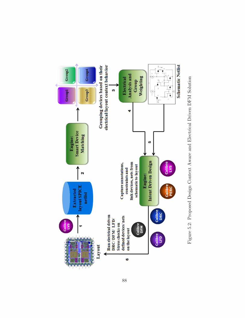
Fig
ure
5.2:
Pro
pos
edD
esig
nC
onte
xt
Aw
are
and
Ele
ctri
cal
Dri
ven
DF
MSol
uti
on
88

2. Grouping the transistors based on their device parameters,
3. Electrical and process analysis performed on samples from each group,
4. Identifying electrical/process hotspots and defining design recommendations on theschematic level,
5. Linking the schematic database to the layout database,
6. Generating and running local physical verification rules checks,
7. Fixing the electrical hotspots on the physical layout.
The first step in this methodology is extracting the SPICE netlist from the layout level.This netlist not only has the circuit information, but also the real-design context and theparasitic information. Theoretically, the netlist can be extracted from the schematic de-sign and the electrical hotspots can still be identified. However, using the SPICE netlistthat is extracted from layout provides insight into layout context that in turn impactsthe electrical behavior of the circuit. This step is followed by using the newly developedDevice Parameters Matching engine. The user has the option to define the list of differentparameters to match. For example, Figure 5.3 shows a sample of the stress related param-eters inside SPICE models [9]. These parameters gets different values based on the designcontext. The Device Parameters Matching engine quickly identifies similar devices thathave similar device parameters values within a given tolerance. The similar devices arethen grouped together. This engine will be described more later in section 5.3.1. The thirdstep in this flow is picking a sample from each group and simulate the different samples,eliminating the need for full-chip electrical simulation. As will be shown in section 5.4,our full chip simulation results prove that all devices in the same group behave the sameelectrically, with negligible differences. Based on the electrical behavior of each group, wecan identify and prioritize the groups based on their electrical variations and how thesevariations would impact the design specifications. This analysis gives us an idea of thecritical devices that are sensitive to process variations. In addition, this information posesseveral physical design information, such as the different critical paths, pair of devices tobe symmetry, net matching, and more. Once these sensitive devices, with their electricalconstraints and physical design recommendations, are identified, another developed toolis used to capture this information and highlight the electrical hotspots on the layoutdatabase. In addition, physical layout rules and lithography-aware checks are generated tobe used in the physical verification step.
89
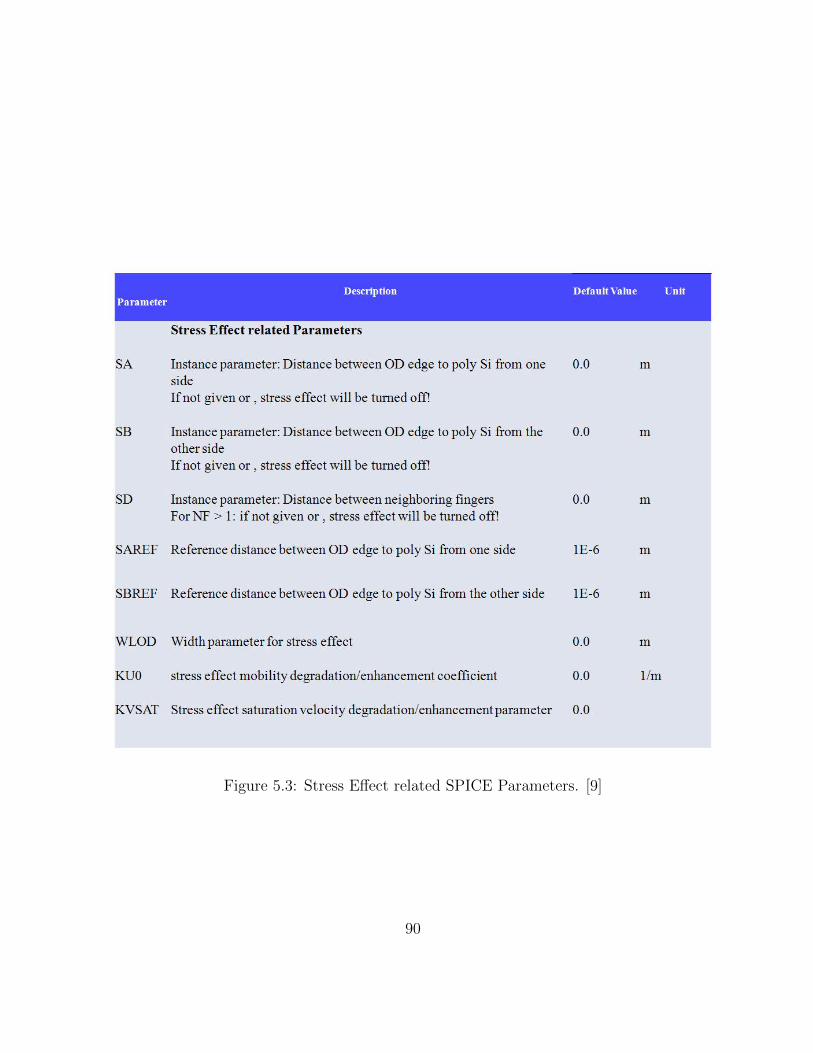
Figure 5.3: Stress Effect related SPICE Parameters. [9]
90

Litho analysis and physical verification are performed using different CalibreTMverificationtools [120]. The physical verification step is performed not on the full-chip data, but onthe specific devices that have been identified as electrical hotspots. Finally, different fixingalgorithms can be applied on the hotspot devices.
In the following subsections, the Device Parameter Matching engine and the IntentDriven Design engine are discussed in more depth.
5.3.1 Smart Device Parameters Matching Engine
Analyzing circuit behavior after extracting lithography and stress effects from the layoutrequires simulating the electrical circuit with the lithography and stress parameters addedto the SPICE model. For digital circuits, the goal is to find transistors whose behaviorwere affected by the lithography process and silicon stress such that their output currentcan no longer drive their load. In other words, we are looking for critical transistors whosedelta current (i.e., difference in current before and after lithography and stress effects areapplied), is larger than a certain value. The process of re-simulating the electrical circuitadds a new stage for designers to consider, which consequently affects the total budgetfor the tapeout flow. Optimizing simulation time for this stage is required to minimizeits impact on the total design budget. The Device Parameters Matching engine is used tooptimize the electrical simulation time. In section 5.4 we illustrate the simulation time andhow it dramatically reduces the runtime using the conventional simulation methods. Com-parisons of the results are also presented, showing no loss in accuracy. The methodology,as described in the pseudo code (Figure 5.4), relies on grouping the circuit transistors intogroups of similar transistors, where similarity is defined as matching the values of theirSPICE model parameters (Figure 5.5). With these groups, we only need to understandthe delta current that occurs in one of the transistor groups to be able to later map thisdelta to all the other transistors in the same group. Matching of each individual parameterdoes not have to be exact; there can be some tolerance in each parameter that depends onthe sensitivity of the electrical behavior of the transistor with respect to that parameter.Adding the tolerances allows for higher groupings or segmentation of the layout into amanageable set of groups of transistors.
Extending the idea of grouping, other models can be applied that further optimizethe simulation time for this stage. For example, one model could store the results of thesimulation into a library where representative transistors from each group are mapped totheir corresponding delta currents. The library could be used to benefit from simulationsof a prior design when creating a new design, or it could be utilized when there are iterativelayout corrections and tests of the same design.
91

Figure 5.4: Pseudo Code for the Device Parameters Matching Algorithm
92
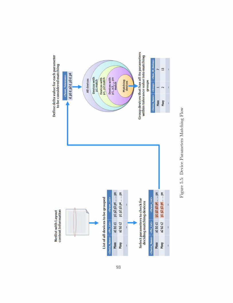
Fig
ure
5.5:
Dev
ice
Par
amet
ers
Mat
chin
gF
low
93
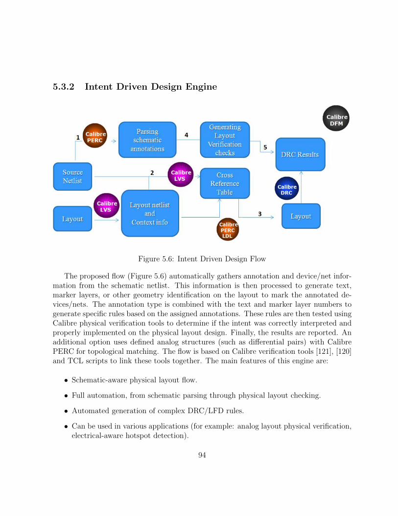
5.3.2 Intent Driven Design Engine
Figure 5.6: Intent Driven Design Flow
The proposed flow (Figure 5.6) automatically gathers annotation and device/net infor-mation from the schematic netlist. This information is then processed to generate text,marker layers, or other geometry identification on the layout to mark the annotated de-vices/nets. The annotation type is combined with the text and marker layer numbers togenerate specific rules based on the assigned annotations. These rules are then tested usingCalibre physical verification tools to determine if the intent was correctly interpreted andproperly implemented on the physical layout design. Finally, the results are reported. Anadditional option uses defined analog structures (such as differential pairs) with CalibrePERC for topological matching. The flow is based on Calibre verification tools [121], [120]and TCL scripts to link these tools together. The main features of this engine are:
• Schematic-aware physical layout flow.
• Full automation, from schematic parsing through physical layout checking.
• Automated generation of complex DRC/LFD rules.
• Can be used in various applications (for example: analog layout physical verification,electrical-aware hotspot detection).
94

The engine flow can be divided into the following steps [122], as shown in Figure 5.6:
1. Parsing the schematic annotations. The flow assumes that the front-end designerplaces annotations on the schematic netlist in a certain format to inform the physicallayout engineers that certain devices and nets have certain electrical constraints orshould have special layout treatments (e.g., device symmetry and orientation, devicewidth segment matching, net balancing, devices placed in cross-quad arrangement,or devices not isolated by guard rings). This step parses the annotations placed inthe schematic netlist and identifies which device or net is involved in which device ornet check. .
2. Linking the schematic database to the layout database. The second steplinks the parsed device/net to its corresponding mate in the layout. The main linkbetween the schematic netlist and the layout is the Layout vs. Schematic (LVS) ruledeck. Running LVS on a design generates the cross-referencing database that linksthe device/net on the schematic to its corresponding mate on the layout and providesthe layout coordinates. To ensure the generated cross-referencing files correctly mapthe equivalent devices, the design must be LVS-clean.
3. Marking the annotated devices and nets on the layout database. For devicechecks, the coordinates obtained from the cross-referencing files place a marking textlayer on each appropriate device. However, because a complete net may be composedfrom many layers, one pair of coordinates is not enough to mark the net for net checks,so all net coordinates are extracted from the LVS database. A script is then usedto organize the data from the first two steps and generate the required text andmarker layers. If there are general checks that must be applied on predefined analogtopological structures, the first two steps are bypassed, and a library of these sets ofstructures is built to mark these devices on the layout.
4. Generating rules based on the annotation readout. When the device/net an-notation calls for a certain procedure corresponding to a certain type of DRC check,the associated text and marker layers are passed to this procedure to automaticallygenerate the required customized rule. The number of generated rules and the asso-ciated devices and nets are identified by the annotations.
5. Running the generated rule files and viewing the results. The generated rulefiles are executed using the Calibre tool suite [120] [121]. Violations are highlightedon the layout.
95

6. Flow Integration. The previous five steps are integrated into a single user interface,which enables the designer to have a push button solution.
The pseudo code description of the engine is shown in Figure 5.7.
5.4 Experiments and Results
In our experiment, we used a 45nm industrial Finite Impulse Response filter (FIR) fullchip (75um x 65um) to detect electrical hotspots. The total number of transistors in theFIR full chip is nearly 23,000 transistors.
5.4.1 Accuracy of the proposed solution
Detecting electrical hotspots using our proposed methodology starts with running thedevice parameters matching engine. With this first step, all transistors based on theirlithography and stress-related devices parameters are matched, such as width, length,and SA and SB parameters (average distance between the gate edge to diffusion edgesmeasured from left and right sides). The device parameters matching engine categorizedthe transistors into 2153 groups. All transistors inside each group were proved to havesimilar electrical behavior. For example, the maximum mismatch error in DC currentamong all transistors in any one group is within the range of 0.001%-0.9%.
Tables 5.1 and 5.2 show examples of two groups as the output from the device pa-rameter matching engine containing a list of the matched devices and the value of theirDC current. It was confirmed visually that the SPICE stress parameters for all the de-vices in one group were matched. For example, devices M1, M3, M6, and M7 had ex-actly the same SPICE stress parameters (SA=1.1e-07, SB=2.08356e-07, SCA=28.0577,SCB=0.0260972, and SCC=0.003727), while nearby transistors, such as M2, had differentSPICE stress parameters (SA=1.1e-07, SB=1.93467e-07, SCA=30.7143, SCB=0.0272008,and SCC=0.00423936).
The flow then picks one transistor from each group as a reference, to calculate the vari-ation of the electrical specifications due to real physical design context for each transistorin that group. When the schematic netlist is first simulated (i.e., no physical design-awareinformation) these stress parameters are not loaded; in this case, the SPICE model cardloads the default stress parameters. In this experiment, the DC current variation between
96

Figure 5.7: Pseudo Code for the Intent Driven Design Engine
97

Table 5.1: Grouping the devices as an output from the Device Parameter Matching Engine-Group 1: contains 4 matched transistors
Device Name X Y DC Current Error %
M1 (ref) 1160 6310 129.1432 0%M3 1160 11350 129.1483 0.00395%M6 1160 18910 129.143 0.0041%M7 1160 21430 129.1496 0.0051%
Table 5.2: Grouping the devices as an output from the Device Parameter Matching Engine-Group 2: contains 8 matched transistors
Device Name X Y DC Current Error %
M13723 (ref) 10400 52815 81.8841 0%M14199 12780 57390 81.8005 -0.1021%M14311 13340 32190 81.505 -0.3612%M14344 13480 52815 81.5493 0.0543%M15024 17400 57390 81.5193 -0.03678%M16104 22860 57855 81.4788 -0.0496%M16131 23000 30135 81.759 0.34389%M16182 23280 54870 81.8042 0.05528%
Table 5.3: Top five device groups experiencing variation in the DC current valuesGroup Index Number of DC Current DC Current Error %
devices simulated from simulated fromdesign aware default
device parameters device parametersnetlist netlist
2049 7 247.406 212.5301 16.4%2153 6 27.2417 32.2432 15.52%1307 5 95.3815 110.862 13.96%12 2 121.1794 140.7287 13.8%
1310 7 95.86 110.6609 13.3%
98
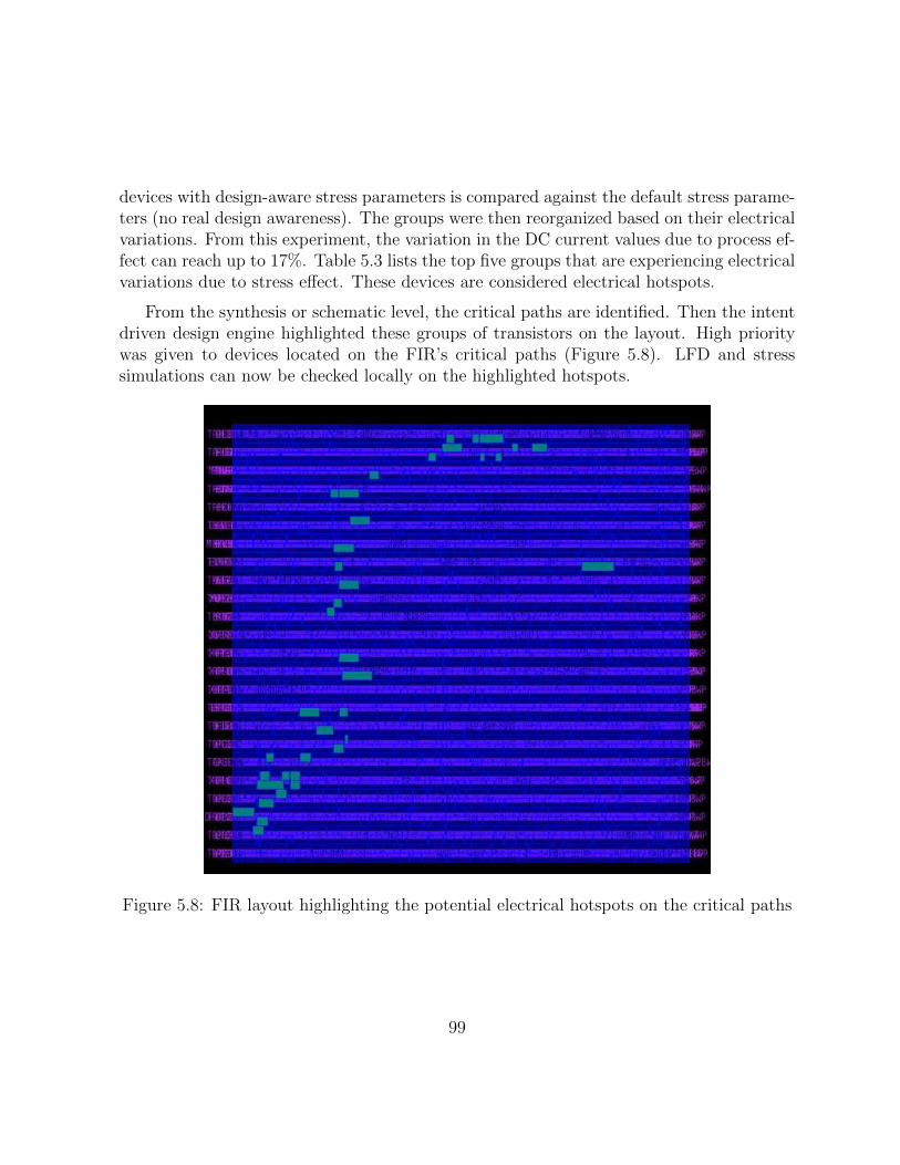
devices with design-aware stress parameters is compared against the default stress parame-ters (no real design awareness). The groups were then reorganized based on their electricalvariations. From this experiment, the variation in the DC current values due to process ef-fect can reach up to 17%. Table 5.3 lists the top five groups that are experiencing electricalvariations due to stress effect. These devices are considered electrical hotspots.
From the synthesis or schematic level, the critical paths are identified. Then the intentdriven design engine highlighted these groups of transistors on the layout. High prioritywas given to devices located on the FIR’s critical paths (Figure 5.8). LFD and stresssimulations can now be checked locally on the highlighted hotspots.
Figure 5.8: FIR layout highlighting the potential electrical hotspots on the critical paths
99

5.4.2 Runtime Analysis
Current state-of-the-art solutions use geometrically-based hotspot detection that dependson identifying problematic structures either by running lithography and stress simulationson full chip, or by using fast techniques such as pattern matching or machine learning.However, because our solution uses electrically-aware hotspot detection, it provides a majoradvantage over these solutions. To illustrate this advantage, we compared the runtimerequired by existing hotspot detections solutions to identify problematic structures againstthe runtime in our proposed solution for grouping the devices. Running the device matchingengine on the FIR (75um x 65um) using one CPU took few seconds to complete. Runtimeof existing solutions were studied and summarized in [123] for 1mm2 chip. Comparingsolutions, as shown in Table 5.4, we can conclude that our grouping solution is extremelyfast compared to existing geometrical-based solutions.
To enable the conventional flows to be electrically-aware, existing solutions must firstextract the electrical netlist and parasitic information from the layout. An electrical sim-ulation is then performed, followed by a calculation of the variation of the electrical speci-fications for each transistor due to real physical design context. The electrical DC currentsimulations of the FIR full chip alone required about one hour. However, using our group-ing methodology, we were able to run electrical simulations on the complete set of devicesin the FIR full chip in nearly two minutes. As mentioned, running the device matchingengine on the FIR took few seconds to complete. This means that the complete flow tooknearly 3 minutes to group, simulate, identify, and locate the electrical hotspots on theFIR full chip layout. Our proposed solution is an encouraging tool that provides a quickstart to locating physical and electrical hotspots on full chip designs. Additional analyticalsimulations can be performed afterwards.
Table 5.4: Result comparison between previous hotspot detection methods and our method[124] [125] [113] [123] [123] Our smart device
A B matching method
Avg real-timerun-time per mm2 1 100 8.5 2.8 0.52 0.4 0.17
runtime slow medium medium fast fast very fast
Run-time calibrated in the unit of CPU hour/mm2 on Linux station with 2.8GHzquad-core processors.1
100

5.5 Summary
In this chapter, a novel methodology is introduced that smartly categorizes all devices inthe full chip by similar electrical and layout context behaviors. Afterwards, electrical andprocess variations analysis is performed on one device in each group, and prioritizes thehotspot groups based on designer’s electrical and process constraints. The main contribu-tions of the proposed CAD solution are listed as follows:
• Developed an electrical-aware and design-driven DFM solution that detects hotspotareas in a full chip design.
• The proposed CAD solution is using a novel device parameter matching engine
• This CAD is an ultra-fast electrical hotspot detector that avoids the time-consumingfull chip simulations previously used for hotspot detection.
• This flow plugs directly into the designer’s existing flows and avoids going throughextensive post layout runtime simulations.
To validate this work, the proposed solution quickly identified electrical hotspot deviceson a 45nm industrial FIR circuit in less than three minutes compared to days and weeksusing the conventional silicon simulation methods.
101

Chapter 6
A Parametric DFM CAD Solutionfor Analog Circuits: ElectricalDriven Hot Spot Detection, Analysisand Correction Flow
6.1 Introduction
Many designers have started to recognize that this push into advanced nodes has exposeda hitherto insignificant set of yield problems. Companies are searching diligently for real-life solutions that address the negative effects of process variation in manufacturing as itapplies to total manufacturing costs. At 130nm and above, physical problems that causecatastrophic failures, such as bridging faults, were always the primary focus of verificationefforts. At those nodes, parametric failures were negligible compared to physical failures.However, at 90nm, parametric failures become significant, and at 65nm, parametric failuresbecome the single most critical yield-limiting factor [114] [115] especially for analog circuits.
Parametric yield issues arise when process variation has not been sufficiently character-ized, such that a circuit may have achieved design closure through standard methodologies,but the silicon performance does not match the simulation results. Both physical and para-metric yield failures have similar negative business implications, in that new circuit designswill fail to meet performance expectations [17].
In this chapter, we present a complete electrical-aware design for manufacturing solutionthat detects, analyzes, and fixes electrical hotspots (e-hotspots) caused by different process
102
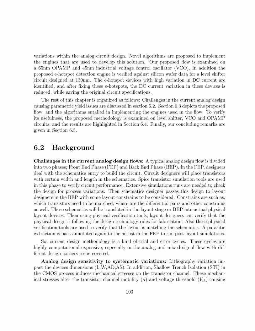
variations within the analog circuit design. Novel algorithms are proposed to implementthe engines that are used to develop this solution. Our proposed flow is examined ona 65nm OPAMP and 45nm industrial voltage control oscillator (VCO). In addition theproposed e-hotspot detection engine is verified against silicon wafer data for a level shiftercircuit designed at 130nm. The e-hotspot devices with high variation in DC current areidentified, and after fixing these e-hotspots, the DC current variation in these devices isreduced, while saving the original circuit specifications.
The rest of this chapter is organized as follows: Challenges in the current analog designcausing parametric yield issues are discussed in section 6.2. Section 6.3 depicts the proposedflow, and the algorithms entailed in implementing the engines used in the flow. To verifyits usefulness, the proposed methodology is examined on level shifter, VCO and OPAMPcircuits, and the results are highlighted in Section 6.4. Finally, our concluding remarks aregiven in Section 6.5.
6.2 Background
Challenges in the current analog design flows: A typical analog design flow is dividedinto two phases; Front End Phase (FEP) and Back End Phase (BEP). In the FEP, designersdeal with the schematics entry to build the circuit. Circuit designers will place transistorswith certain width and length in the schematics. Spice transistor simulation tools are usedin this phase to verify circuit performance. Extensive simulations runs are needed to checkthe design for process variations. Then schematics designer passes this design to layoutdesigners in the BEP with some layout constrains to be considered. Constrains are such as;which transistors need to be matched; where are the differential pairs and other constrainsas well. These schematics will be translated in the layout stage or BEP into actual physicallayout devices. Then using physical verification tools, layout designers can verify that thephysical design is following the design technology rules for fabrication. Also these physicalverification tools are used to verify that the layout is matching the schematics. A parasiticextraction is back annotated again to the netlist in the FEP to run post layout simulations.
So, current design methodology is a kind of trial and error cycles. These cycles arehighly computational expensive; especially in the analog and mixed signal flow with dif-ferent design corners to be covered.
Analog design sensitivity to systematic variations: Lithography variation im-pact the devices dimensions (L,W,AD,AS). In addition, Shallow Trench Isolation (STI) inthe CMOS process induces mechanical stresses on the transistor channel. These mechan-ical stresses alter the transistor channel mobility (µ) and voltage threshold (Vth) causing
103
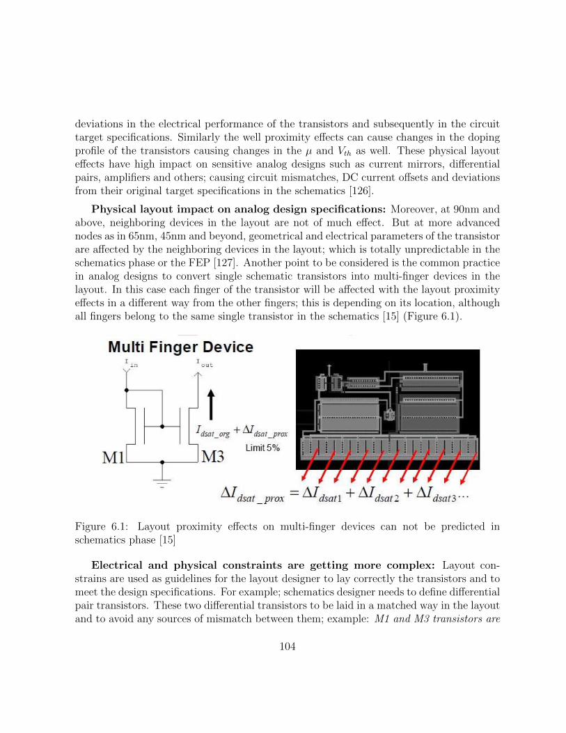
deviations in the electrical performance of the transistors and subsequently in the circuittarget specifications. Similarly the well proximity effects can cause changes in the dopingprofile of the transistors causing changes in the µ and Vth as well. These physical layouteffects have high impact on sensitive analog designs such as current mirrors, differentialpairs, amplifiers and others; causing circuit mismatches, DC current offsets and deviationsfrom their original target specifications in the schematics [126].
Physical layout impact on analog design specifications: Moreover, at 90nm andabove, neighboring devices in the layout are not of much effect. But at more advancednodes as in 65nm, 45nm and beyond, geometrical and electrical parameters of the transistorare affected by the neighboring devices in the layout; which is totally unpredictable in theschematics phase or the FEP [127]. Another point to be considered is the common practicein analog designs to convert single schematic transistors into multi-finger devices in thelayout. In this case each finger of the transistor will be affected with the layout proximityeffects in a different way from the other fingers; this is depending on its location, althoughall fingers belong to the same single transistor in the schematics [15] (Figure 6.1).
Figure 6.1: Layout proximity effects on multi-finger devices can not be predicted inschematics phase [15]
Electrical and physical constraints are getting more complex: Layout con-strains are used as guidelines for the layout designer to lay correctly the transistors and tomeet the design specifications. For example; schematics designer needs to define differentialpair transistors. These two differential transistors to be laid in a matched way in the layoutand to avoid any sources of mismatch between them; example: M1 and M3 transistors are
104

differential transistors to be matched in gate length within 5% tolerance. With the advancesin the IC process technologies and the migration of analog designs from 130nm/90nm to65nm/45nm and beyond, the proximity constrains have to be considered. For example;Idsat in M3 not to exceed 5% due to layout proximity effects, this constrain can show upin the design cycle of a DC current bias cell (a common block in analog designs). In thetraditional design flow, such new constrains are difficult to be handled either on the FEPside or on the BEP side.
There are some ways currently used in the design flow to account for layout effectsbut with drawbacks. For example, on the FEP side, CAD engineers can provide the ICschematics designers with Process Design Kit (PDK). This PDK gives estimates for thelayout proximity effects in schematics. However this way is not accurate as proximityeffects cant be accurately predicted unless the layout is fully finished. On the other side,layout designers do not use spice transistor simulations tools to perform simulations topredict electrical changes in performance due to the layout drawn. Also, it is not feasibleto add a time consuming electrical simulator to the layout drawing phase as this is nota common practice and is fully disrupting the normal design flow. Thats why a differentmethodology is needed to handle such issues in the design cycle and this is proposed in thefollowing CAD solution.
6.3 Proposed Flow Overview: Electrical Hot Spot De-
tection, Analysis and Correction Flow
The proposed CAD flow incorporates some key features that enable the proposed para-metric DFM solution and differentiate it from the existing solutions. These features arehighlighted as follows:
• Electrical-aware DFM solution
Today, many of the approaches that are commonly referred to as physical DFMtechniques only address catastrophic defects and systematic process variations. Thesetechniques include spreading wires, doubling vias, identification of critical areas inthe circuit that are especially susceptible to defects, and identification of proximityeffects caused by the lithography process. However, physical DFM tools are purely”geometric”, in that they work to preserve shape fidelity without any knowledgeof the impact on the electrical characteristics of the shapes that are manufacturedin silicon [112]. While these techniques have proven useful in reducing functional
105
failures and increasing overall yield by a few percentage points, they completelyignore the more important category of parametric failures. The proposed solutionpresented in this chapter specifically helps to address the parametric performancemodeling problems encountered at smaller geometries. As this solution drives designrequirements into physical layout design and moves layout awareness upstream intodesign, useful information about the design (on the physical and electrical level) iscaptured, analyzed, and simulated. Deviations in the electrical characteristics due tophysical layout and process variations, are identified and highlighted on the design.These deviations are referred as electrical hotspots (e-hotspots).
• Complete Parametric DFM Solution for Analog Designs: Detection, Anal-ysis and Correction
Several prototype techniques exemplify how parametric DFM solutions can take intoaccount design-specific information to improve design analyses and enhancements[112]. Examples include (1) iso-dense awareness of pitch-dependent through-focusCD variation, to reduce timing guardbands and improve timing robustness [128]; (2)Selfcompensating design techniques that minimize the inherent sensitivity of criticalpaths to various sources of process variation [129]. Other parametric DFM solutionsare focused on analyzing and detecting the electrical variations, although some so-lutions include DFM-aware place-and-route remedies that propose e-hotspot fixes.However, all of these solutions mainly address digital designs [130]. In our work,we propose a variability-aware parametric DFM solution that detects and fixes e-hotspots for analog circuits.
• Eliminate time-consuming full circuit SPICE simulations
Analyzing circuit behavior after extracting lithography and stress effects from thelayout requires simulating the electrical circuit with the lithography and stress pa-rameters added to the SPICE model. For analog circuits, the goal is to find transistorswhose behavior are affected by the lithography process and silicon stress such thattheir DC current can impact the circuit specifications (such as gain, phase margin,frequency response). In other words, designers are looking for transistors whose elec-trical parameters such as current, Vth, and mobility experience variations before andafter lithography and stress effects are applied and violates the designers’ electricalconstraints. This process of re-simulating the electrical circuit adds a new stageto the process flow, which consequently increases the total budget for the tapeoutflow. To optimize the electrical simulation time and minimize the impact on thetotal design budget, the proposed parametric DFM solution can detect the electrical
106
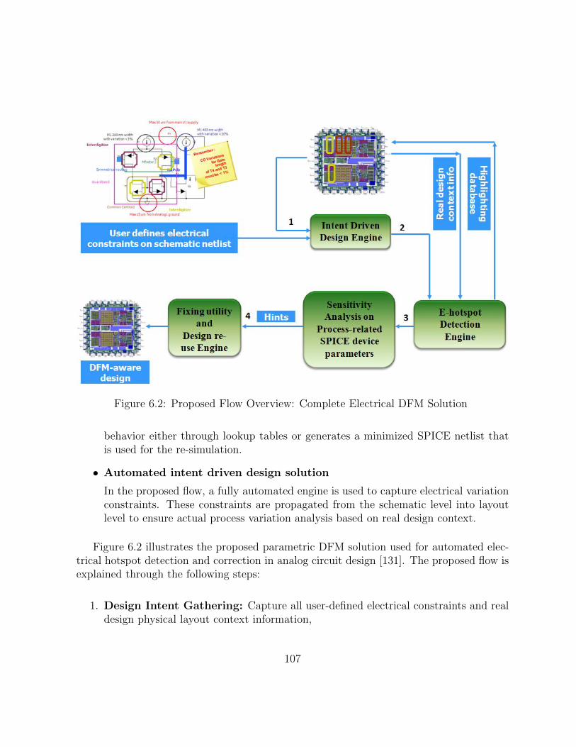
Figure 6.2: Proposed Flow Overview: Complete Electrical DFM Solution
behavior either through lookup tables or generates a minimized SPICE netlist thatis used for the re-simulation.
• Automated intent driven design solution
In the proposed flow, a fully automated engine is used to capture electrical variationconstraints. These constraints are propagated from the schematic level into layoutlevel to ensure actual process variation analysis based on real design context.
Figure 6.2 illustrates the proposed parametric DFM solution used for automated elec-trical hotspot detection and correction in analog circuit design [131]. The proposed flow isexplained through the following steps:
1. Design Intent Gathering: Capture all user-defined electrical constraints and realdesign physical layout context information,
107
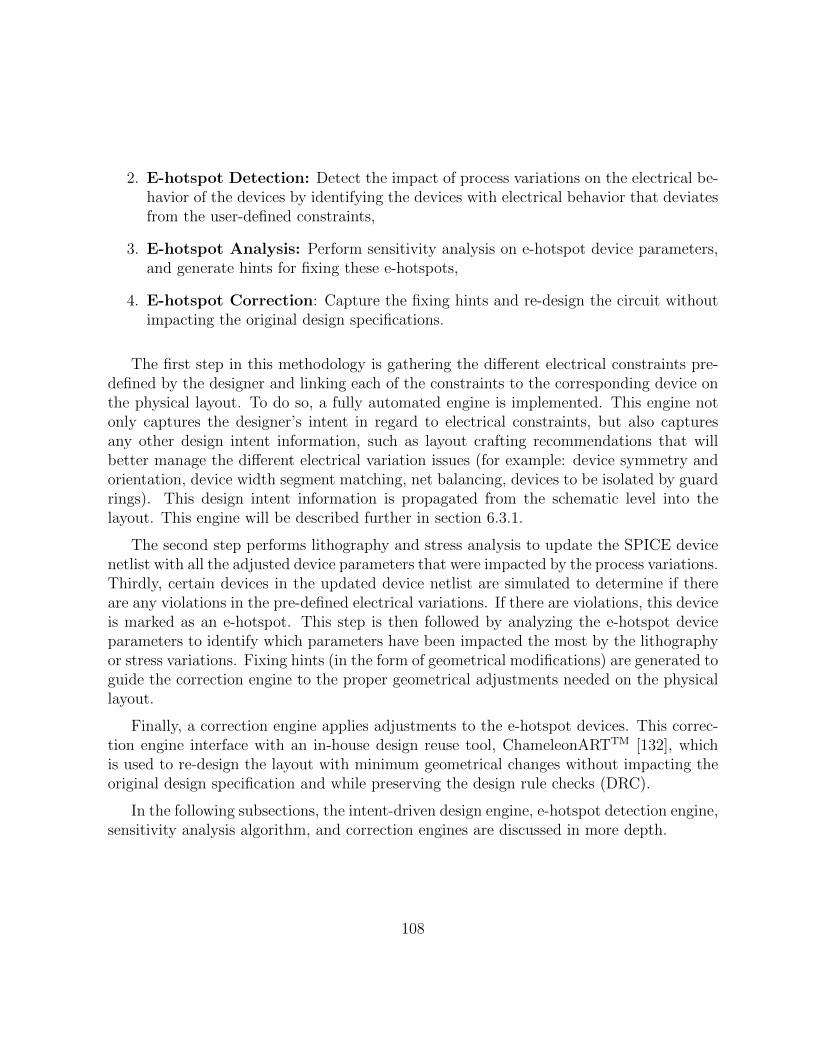
2. E-hotspot Detection: Detect the impact of process variations on the electrical be-havior of the devices by identifying the devices with electrical behavior that deviatesfrom the user-defined constraints,
3. E-hotspot Analysis: Perform sensitivity analysis on e-hotspot device parameters,and generate hints for fixing these e-hotspots,
4. E-hotspot Correction: Capture the fixing hints and re-design the circuit withoutimpacting the original design specifications.
The first step in this methodology is gathering the different electrical constraints pre-defined by the designer and linking each of the constraints to the corresponding device onthe physical layout. To do so, a fully automated engine is implemented. This engine notonly captures the designer’s intent in regard to electrical constraints, but also capturesany other design intent information, such as layout crafting recommendations that willbetter manage the different electrical variation issues (for example: device symmetry andorientation, device width segment matching, net balancing, devices to be isolated by guardrings). This design intent information is propagated from the schematic level into thelayout. This engine will be described further in section 6.3.1.
The second step performs lithography and stress analysis to update the SPICE devicenetlist with all the adjusted device parameters that were impacted by the process variations.Thirdly, certain devices in the updated device netlist are simulated to determine if thereare any violations in the pre-defined electrical variations. If there are violations, this deviceis marked as an e-hotspot. This step is then followed by analyzing the e-hotspot deviceparameters to identify which parameters have been impacted the most by the lithographyor stress variations. Fixing hints (in the form of geometrical modifications) are generated toguide the correction engine to the proper geometrical adjustments needed on the physicallayout.
Finally, a correction engine applies adjustments to the e-hotspot devices. This correc-tion engine interface with an in-house design reuse tool, ChameleonARTTM [132], whichis used to re-design the layout with minimum geometrical changes without impacting theoriginal design specification and while preserving the design rule checks (DRC).
In the following subsections, the intent-driven design engine, e-hotspot detection engine,sensitivity analysis algorithm, and correction engines are discussed in more depth.
108

6.3.1 Intent Driven Design Engine
The proposed intent-driven design engine (Figure 6.3), assumes that the front-end designerplaces design constraints in the form of annotations on the schematic netlist that areextracted from the electrical analysis stage. These annotations inform the physical layoutengineers that the electrical behavior of certain devices and nets should be preserved afterthe physical layout implementation. Afterwards, this information is processed to generatetext and marker layers on the layout to mark the annotated devices/nets. The type ofannotation, together with the text and marker layer numbers, is used afterwards by thee-hotspot detection engine to generate a minimized SPICE netlist. The flow goes throughthe following steps:
1. Parsing the schematic annotations,
2. Linking the schematic database to the layout database,
3. Identifying the annotated devices and nets on the layout database.
The first step parses the annotations placed in the schematic netlist (such as electricalvariation constraints or layout recommendations). This step also correlates each device/netwith its corresponding design constraint check; this information may be reported in aseparate output file containing each device or net and its associated annotation.
The second step links the parsed device or net to its corresponding mate in the layout.The main link between the schematic netlist and the layout is the Layout versus Schematic(LVS) rule file, as running LVS on a design generates the cross-referencing files that identifywhich device or net on the schematic corresponds to which device or net on the layout. Italso assigns, and reports a corresponding coordinate for that device or net on the layout.For this part of the step to run correctly, the design must be LVS-clean, to ensure thegenerated cross-referencing files correctly map to the equivalent devices.
The third step uses the coordinates obtained from the cross-referencing files and placesa text layer on each appropriate device. In this step, a software script is used to organizeand apply the data obtained from the first two steps to generate the required text andmarker layers. Because a net may be composed of many layers, one pair of coordinatesis not enough to mark a complete net. For the net checks, the net coordinates from theLVS database are extracted to mark the net. When the device/net annotation calls foran electrical simulation, the associated text and marker layers are passed, along with aprocedure that generates the required SPICE testcase.
109
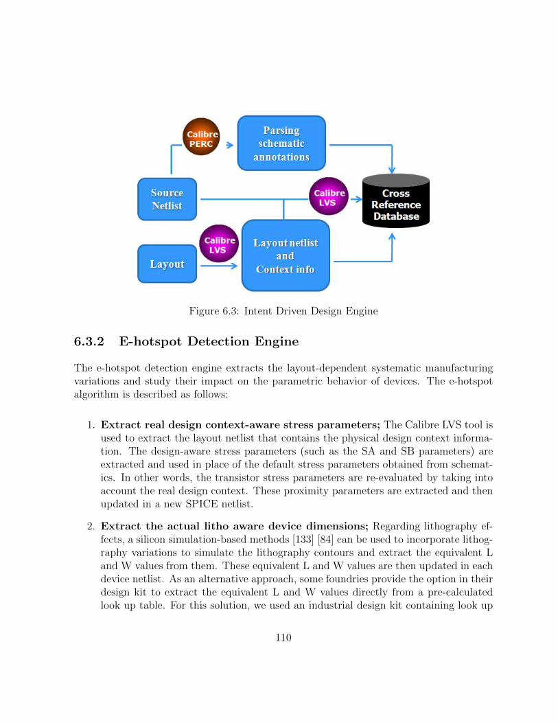
Figure 6.3: Intent Driven Design Engine
6.3.2 E-hotspot Detection Engine
The e-hotspot detection engine extracts the layout-dependent systematic manufacturingvariations and study their impact on the parametric behavior of devices. The e-hotspotalgorithm is described as follows:
1. Extract real design context-aware stress parameters; The Calibre LVS tool isused to extract the layout netlist that contains the physical design context informa-tion. The design-aware stress parameters (such as the SA and SB parameters) areextracted and used in place of the default stress parameters obtained from schemat-ics. In other words, the transistor stress parameters are re-evaluated by taking intoaccount the real design context. These proximity parameters are extracted and thenupdated in a new SPICE netlist.
2. Extract the actual litho aware device dimensions; Regarding lithography ef-fects, a silicon simulation-based methods [133] [84] can be used to incorporate lithog-raphy variations to simulate the lithography contours and extract the equivalent Land W values from them. These equivalent L and W values are then updated in eachdevice netlist. As an alternative approach, some foundries provide the option in theirdesign kit to extract the equivalent L and W values directly from a pre-calculatedlook up table. For this solution, we used an industrial design kit containing look up
110
tables for the equivalent L and W values according to their context. Hence, the lithocontour extraction flow through simulation is avoided.
3. Calculate electrical variations;
Figure 6.4: Ids vs. Distance from STI boundary Typical 0.13um process [16]
Lithography, STI and well proximity effects cause a shift in transistor dimensions,mobility and threshold voltage, which cause a shift in the Idsat [126]. All these shiftscan be detected using DC analysis for each device. Figure 6.4 is a plot showing anexample of how Idsat varies as a function of distance from the STI boundary whenbiased at low current where Vgs is within 200 mV of threshold. This has importantramifications in staple circuits of analog design like current mirrors and differentialamplifiers. Figure 6.4 illustrates that Idsat mismatches as large as 30% can be possibleso in extreme cases. An example of a DC parametric failure for an amplifier circuitcaused by stress effects, is illustrated in [16], proposing a solution to catch parametricfailures by monitoring the DC bias currents in a post-layout extracted simulation.
111

Three different approaches are adopted in the proposed flow to calculate the shift inthe Idsat:
• Use built in functions exactly similar to the transistor model equations to cal-culate the variations in Vth, mobility, device dimensions and then pass thesevariations to look up table that consists of a list of a pre-simulated values ofIdsat as function of Vth, mobility, device dimensions. This flow avoids introduc-ing more simulations, however in this case there is accuracy tradeoff dependingon the lookup table database [15].
• Generate a minimized SPICE netlist updated with process-aware parameters foreach of the annotated devices in the schematic design. In order to get accuratevalues, and once the process-aware netlist is generated for each device withelectrical constraints in the design, a SPICE simulation is performed.
• For small sized analog circuits, there is an option to simulate the completecircuit. Afterwards variations in percentage for absolute and matched devicesare calculated.
4. Highlight violations; Compare the original electrical behavior versus the resultsfrom the extracted device parameter. Whenever a device violates the user-definedelectrical constraints, that device is highlighted as e-hotspot devices. Below is a sam-ple of the output from the e-hotspot Detection Engine: List of the current variationsin each device in the design followed by list of devices that violated the designerconstraints.
##################################################################
############## Device Reports #################
##################################################################
Id variation in device M12: -7.90739272034%
Id variation in device M50: -5.56061578377%
Id variation in device M36: 3.60789458673%
Id variation in device M40: 2.35862956526%
##################################################################
############## Device Violations #################
##################################################################
Violation: M12 absolute Id variation = 7.90739272034 > 5%
Violation: M50 absolute Id variation = 5.56061578377 > 5%
##################################################################
112
This flow enables the layout engineers to identify areas in the layout considered to bee-hotspots and also checks that the designer’s intent has been correctly passed and properlyimplemented on the physical layout design.
6.3.3 Sensitivity Analysis Algorithm
The goal of this step is to identify the exact source of the layout effects on integrated circuitperformance.
Sensitivity analysis of the saturation current Idsat can be expressed as [134]:
δIdsatIdsat
= Σ(δIdsatδxi
xiIdsat
)δxixi
(6.1)
where xi, denotes average of Vth, Cox, L and any other parameters in interest, whileδxi denotes deviation for each parameters. The average and standard deviation of theindependent SPICE parameters can be extracted from the layout aware SPICE netlist.The percentage of each component of Idsat standard deviation is calculated. Based on thisresult, it can concluded if the Idsat of specific device varies due to lithography effects (L,W)or stress effects (Vth, mobility) or even CMP effects (Tox).
As stress effects are one of the main causes of electrical variations in analog and mixedsignal designs [15], we will further apply equation 6.1 on stress related parameters. Studiesshow that the width of the well proximity effects and shallow trench isolation (STI) effectsinduce mechanical stresses on the transistor channel, causing electrical and timing changesin the circuit performance [80] [5]. Hence, the electrical SPICE simulation of a schematiclevel netlist can perform differently when in a real design environment. Shallow TrenchIsolation (STI) in the CMOS process induces mechanical stresses on the transistor channel.These mechanical stresses alter the transistor channel mobility µ and voltage threshold Vthcausing deviations in the electrical performance of the transistors and subsequently inthe circuit target specifications. Similarly the well proximity effects can cause changesin the doping profile of the transistors causing changes in the µ and Vth as well. Thesephysical layout effects have high impact on sensitive analog designs such as current mirrors,differential pairs, amplifiers and others; causing circuit mismatches [135], DC current offsetsand deviations from their original target specifications in the schematics.
Stress modeling equations are available in Berkley BSIM4 manuals [9]. The followingis the Vth equation changes due to stress effects [15]:
113

V TH0 = V TH0original +KTH0
Kstress vth0
∗ (Inv sa+ Inv sb− Inv saref − Inv sbref ) (6.2)
∆V TH =KTH0
Kstress vth0
∗ (Inv sa+ Inv sb− Inv saref − Inv sbref ) (6.3)
Assuming that mobility relative change is propotional to stress distribution. It can bedescribed as function of SA, SB(LOD effect), L, W, and T dependence [9]:
∆µ =KU0
Kstress u0
∗ (Inv sa+ Inv sb) (6.4)
Studying these equations closely; they are totally dependent on two different kinds ofparameters:
1. Layout geometrical parameters; such as Inv sa and Inv sb. Where
Inv sa =1
SA + 0.5 ∗ Ldrawn
(6.5)
Inv sb =1
SB + 0.5 ∗ Ldrawn
(6.6)
2. Process model technology parameters; such asKTH0, KU0, Kstress u0 andKstress vth0.
The layout geometrical parameters will be extracted using the physical verification tooland the process technology parameters are available as constants in the spice model cardsof the target IC technology.
As the saturation current is one of the main components in analog designs and it ishighly dependent on µ, Vth and also saturation velocity. The following equations repre-sent changes in Idsat (using the simplified Idsat equations) due to stress effects on Vth andmobility:
Idsat =1
2µoCox
W
L∗ (Vgs − Vth)2 (6.7)
114

δIdsat =δIdsatδµo
δµo +δIdsatδVth
δVth (6.8)
where
δIdsatδµo
=1
2Cox
W
L∗ (Vgs − Vth)2 (6.9)
δIdsatδVth
= −µoCoxW
L∗ (Vgs − Vth) (6.10)
and δVth is defined in equation 6.2 and δµo is defined in equation 6.4.
Schematic designers already have the operating point for all nodes of their circuitincluding transistor gate-source voltage (Vgs) and transistor drain-source voltage (Vds).Schematic designers can pass transistor voltages and any other required electrical constrainssimilar to the layout constrains through the intent driven design engine. Applying theseparameters to the target electrical equations will give the layout designer approximatevalues for electrical changes due to layout proximity effects. This is applied with no needto have a simulator on the layout side.
Using the suggested flow, and knowing the main contributor in Idsat variation, a layouthint information to minimize the process effects, is provided. Speaking of stress parame-ters, the diffusion edges are increased in steps (Figure 6.5). Each time the diffusion edgeis changed, multiple parameters in the transistor are impacted, such as Area Drain Ca-pacitance (AD), Area Source Capacitance (AS), PD, PS, NRD, and NRS, as well as thestress and Nwell Proximity parameters (SA, SB, SCA, SCB and SCC). For each of thesechanges, the transistor model parameters in the SPICE netlist are updated, and simulationruns are performed to obtain the electrical variation change. In addition DRC is appliedto make sure that the suggested movements do not violate any DRC rules. The diffusionedge values that correspond to the minimum change are identified as the fixing hint forthe e-hotspot correction engine. Below is an example of the hint file generated:
###################################################################
//Cell Name:
PLL_TxVCO 1
//Layers Name
check.copy::M2_MWC_COPY = COPY M2_MSC
//First Hint
115
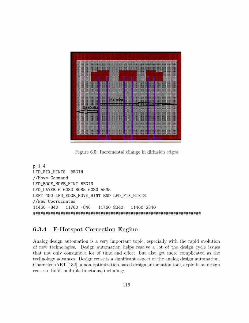
Figure 6.5: Incremental change in diffusion edges
p 1 4
LFD_FIX_HINTS BEGIN
//Move Command
LFD_EDGE_MOVE_HINT BEGIN
LFD_LAYER 6 6080 8085 6080 5535
LEFT 450 LFD_EDGE_MOVE_HINT END LFD_FIX_HINTS
//New Coordinates
11460 -840 11760 -840 11760 2340 11460 2340
###################################################################
6.3.4 E-Hotspot Correction Engine
Analog design automation is a very important topic, especially with the rapid evolutionof new technologies. Design automation helps resolve a lot of the design cycle issuesthat not only consume a lot of time and effort, but also get more complicated as thetechnology advances. Design reuse is a significant aspect of the analog design automation.ChameleonART [132], a non-optimization based design automation tool, exploits on designreuse to fulfill multiple functions, including:
116
• Netlist migration between a source and a target technology,
• Layout migration and compaction to a target technology,
• Processing tasks on the output layout to preserve a clean DRC profile.
The ChameleonART layout compaction engine moves all edges relative to each other,while respecting the target DRC constraints. This kind of compaction is useful for migra-tion between different technologies, preserving the original layout intelligence inherent inthe design, such as the topology, the symmetry and other design aspects. However, thedesign may incur a change in the layout shape and presence of void spaces due to the com-paction. When used as a correction utility within the e-hotspot fixing flow, ChameleonARTis limited to moving the faulty edges or implementing the user-defined fix hints, then ad-justing other dependent edges. This fixing technique ensures minimum movement of mostof the edges and polygons, while preserving DRC constraints and the original layout intelli-gence. The electrical variation flow provides ChameleonART with the layout changes thatcompensate for the effect of stress and lithography. These changes are defined in terms ofminor device dimensions or stress dimension changes such as SA or SB in a multi-fingerdevice. The ChameleonART tool implements these changes and adjusts any dependentedges, to preserve both a clean DRC profile and the design intelligence, while minimiz-ing changes in all other edges and polygons. ChameleonART is characterized by its fastruntime and clean physical verification results.
The main layout correction algorithm (Figure 6.6) is described as follows:
1. The correction flow starts with the layout pre-processing stage. This pre-processingstep helps identify a correct relative coverage of layers, lower number of edges, andother techniques that ensure the correct and optimum number of constraints.
2. Next, the tool generates the different types of constraints that guide the fixing pro-cess, such as target DRC constraints, device constraints, symmetry, and routingconstraints. In addition, there are many directives that must be set initially forproper fixing, such as flat/hierarchical migration, use of basic/recommended DRCrules as the target DRC constraints, type of passive devices handling, and type ofhandle routing with different algorithms and user defined constraints.
3. Finally, correcting the e-hotspot by localized layout compaction, decreasing the num-ber of edges, constraints, or layers. The post-processing stage generates a suitableversion for the DRC/LVS verification phase.
The pseudo code of the layout correction algorithm is described in Figure 6.7
117
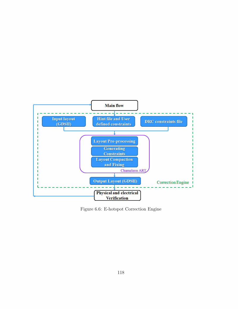
Figure 6.6: E-hotspot Correction Engine
118

Figure 6.7: Pseudo Code for the E-hotspot Correction Engine
119
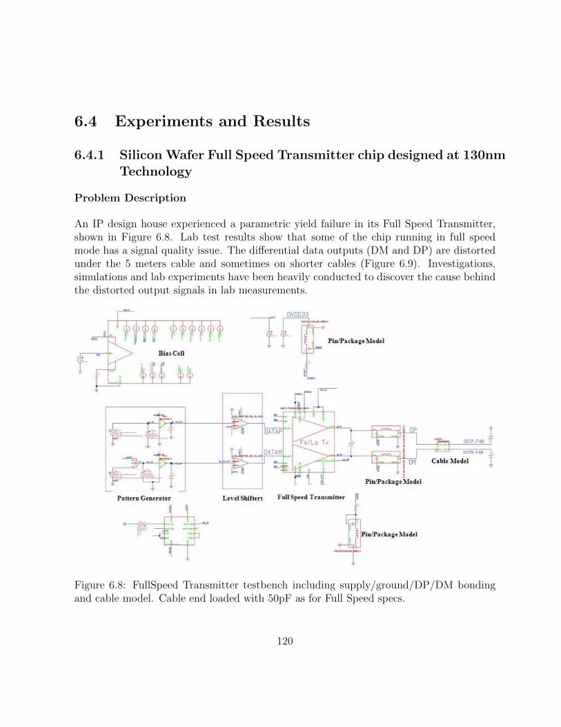
6.4 Experiments and Results
6.4.1 Silicon Wafer Full Speed Transmitter chip designed at 130nmTechnology
Problem Description
An IP design house experienced a parametric yield failure in its Full Speed Transmitter,shown in Figure 6.8. Lab test results show that some of the chip running in full speedmode has a signal quality issue. The differential data outputs (DM and DP) are distortedunder the 5 meters cable and sometimes on shorter cables (Figure 6.9). Investigations,simulations and lab experiments have been heavily conducted to discover the cause behindthe distorted output signals in lab measurements.
Figure 6.8: FullSpeed Transmitter testbench including supply/ground/DP/DM bondingand cable model. Cable end loaded with 50pF as for Full Speed specs.
120
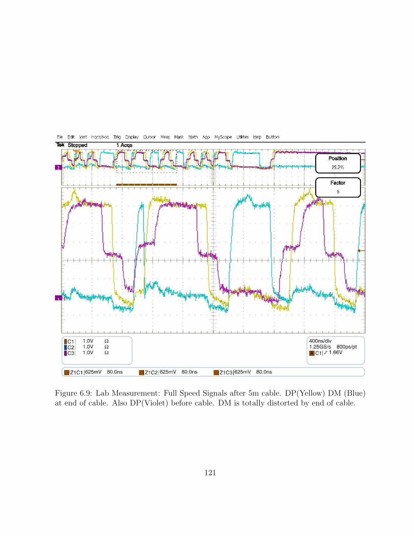
Figure 6.9: Lab Measurement: Full Speed Signals after 5m cable. DP(Yellow) DM (Blue)at end of cable. Also DP(Violet) before cable. DM is totally distorted by end of cable.
121
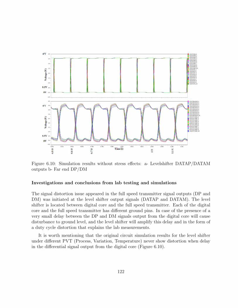
Figure 6.10: Simulation results without stress effects: a- Levelshifter DATAP/DATAMoutputs b- Far end DP/DM
Investigations and conclusions from lab testing and simulations
The signal distortion issue appeared in the full speed transmitter signal outputs (DP andDM) was initiated at the level shifter output signals (DATAP and DATAM). The levelshifter is located between digital core and the full speed transmitter. Each of the digitalcore and the full speed transmitter has different ground pins. In case of the presence of avery small delay between the DP and DM signals output from the digital core will causedisturbance to ground level, and the level shifter will amplify this delay and in the form ofa duty cycle distortion that explains the lab measurements.
It is worth mentioning that the original circuit simulation results for the level shifterunder different PVT (Process, Variation, Temperature) never show distortion when delayin the differential signal output from the digital core (Figure 6.10).
122
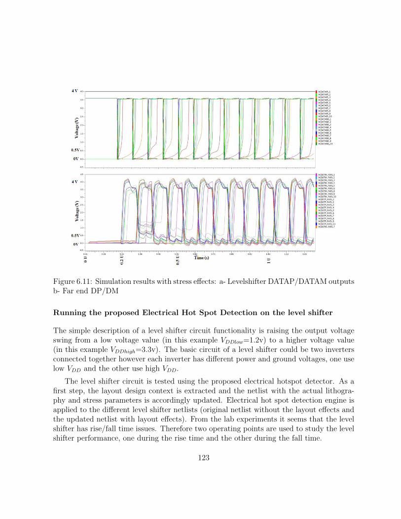
Figure 6.11: Simulation results with stress effects: a- Levelshifter DATAP/DATAM outputsb- Far end DP/DM
Running the proposed Electrical Hot Spot Detection on the level shifter
The simple description of a level shifter circuit functionality is raising the output voltageswing from a low voltage value (in this example VDDlow=1.2v) to a higher voltage value(in this example VDDhigh=3.3v). The basic circuit of a level shifter could be two invertersconnected together however each inverter has different power and ground voltages, one uselow VDD and the other use high VDD.
The level shifter circuit is tested using the proposed electrical hotspot detector. As afirst step, the layout design context is extracted and the netlist with the actual lithogra-phy and stress parameters is accordingly updated. Electrical hot spot detection engine isapplied to the different level shifter netlists (original netlist without the layout effects andthe updated netlist with layout effects). From the lab experiments it seems that the levelshifter has rise/fall time issues. Therefore two operating points are used to study the levelshifter performance, one during the rise time and the other during the fall time.
123

The proposed flow is able to detect devices inside the level shifter that have parametricperformance issues, as follows:
Case1: Rise Time
##################################################################
############## Device Reports #################
##################################################################
Id variation in device Mout_p: 75.183745307 %
##################################################################
############## Device Violations #################
##################################################################
Violation: Mout_p absolute Id variation = 75.183745307% > 5%
##################################################################
Case2: Fall Time
##################################################################
############## Device Reports #################
##################################################################
Id variation in device Mout_n: 0.63810392%
##################################################################
############## Device Violations #################
##################################################################
##################################################################
The highlighted e-hotspot device Mout p is the output stage device for the level shifter.The stress effects on this device impact the device’s mobility, Vth and hence affect Idsatand hence the rise time to load the following stage causing signal distortion, matchingsimulation results and lab measurements.
Full circuit simulations are repeated after extracting the actual layout stress effects, thesimulations results (Figure 6.11) illustrated signal distortion from the level shifter output,concluding that the updated level shifter netlist (with layout stress effects) gave similarperformance as the lab measurements due to the stress effects, which were not accountedduring the design verification stage. This experiment illustrates the huge benefit of havingthis flow in the design verification stage, as an early stage detector for electrical hotspotsand avoids wafer parametric yield failures. The physical layout was not shared by the IPdesign house, therefore the correction stage was not applied in this test case.
124
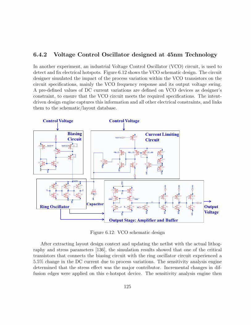
6.4.2 Voltage Control Oscillator designed at 45nm Technology
In another experiment, an industrial Voltage Control Oscillator (VCO) circuit, is used todetect and fix electrical hotspots. Figure 6.12 shows the VCO schematic design. The circuitdesigner simulated the impact of the process variation within the VCO transistors on thecircuit specifications, mainly the VCO frequency response and its output voltage swing.A pre-defined values of DC current variations are defined on VCO devices as designer’sconstraint, to ensure that the VCO circuit meets the required specifications. The intent-driven design engine captures this information and all other electrical constraints, and linksthem to the schematic/layout database.
Figure 6.12: VCO schematic design
After extracting layout design context and updating the netlist with the actual lithog-raphy and stress parameters [136], the simulation results showed that one of the criticaltransistors that connects the biasing circuit with the ring oscillator circuit experienced a5.5% change in the DC current due to process variations. The sensitivity analysis enginedetermined that the stress effect was the major contributor. Incremental changes in dif-fusion edges were applied on this e-hotspot device. The sensitivity analysis engine then
125
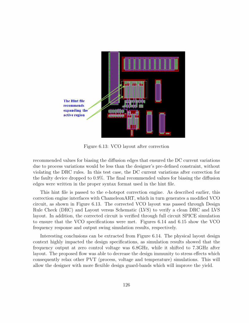
Figure 6.13: VCO layout after correction
recommended values for biasing the diffusion edges that ensured the DC current variationsdue to process variations would be less than the designer’s pre-defined constraint, withoutviolating the DRC rules. In this test case, the DC current variations after correction forthe faulty device dropped to 0.9%. The final recommended values for biasing the diffusionedges were written in the proper syntax format used in the hint file.
This hint file is passed to the e-hotspot correction engine. As described earlier, thiscorrection engine interfaces with ChameleonART, which in turn generates a modified VCOcircuit, as shown in Figure 6.13. The corrected VCO layout was passed through DesignRule Check (DRC) and Layout versus Schematic (LVS) to verify a clean DRC and LVSlayout. In addition, the corrected circuit is verified through full circuit SPICE simulationto ensure that the VCO specifications were met. Figures 6.14 and 6.15 show the VCOfrequency response and output swing simulation results, respectively.
Interesting conclusions can be extracted from Figure 6.14. The physical layout designcontext highly impacted the design specifications, as simulation results showed that thefrequency output at zero control voltage was 6.8GHz, while it shifted to 7.3GHz afterlayout. The proposed flow was able to decrease the design immunity to stress effects whichconsequently relax other PVT (process, voltage and temperature) simulations. This willallow the designer with more flexible design guard-bands which will improve the yield.
126
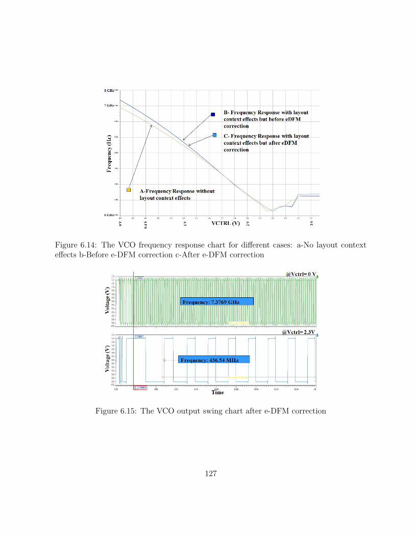
Figure 6.14: The VCO frequency response chart for different cases: a-No layout contexteffects b-Before e-DFM correction c-After e-DFM correction
Figure 6.15: The VCO output swing chart after e-DFM correction
127
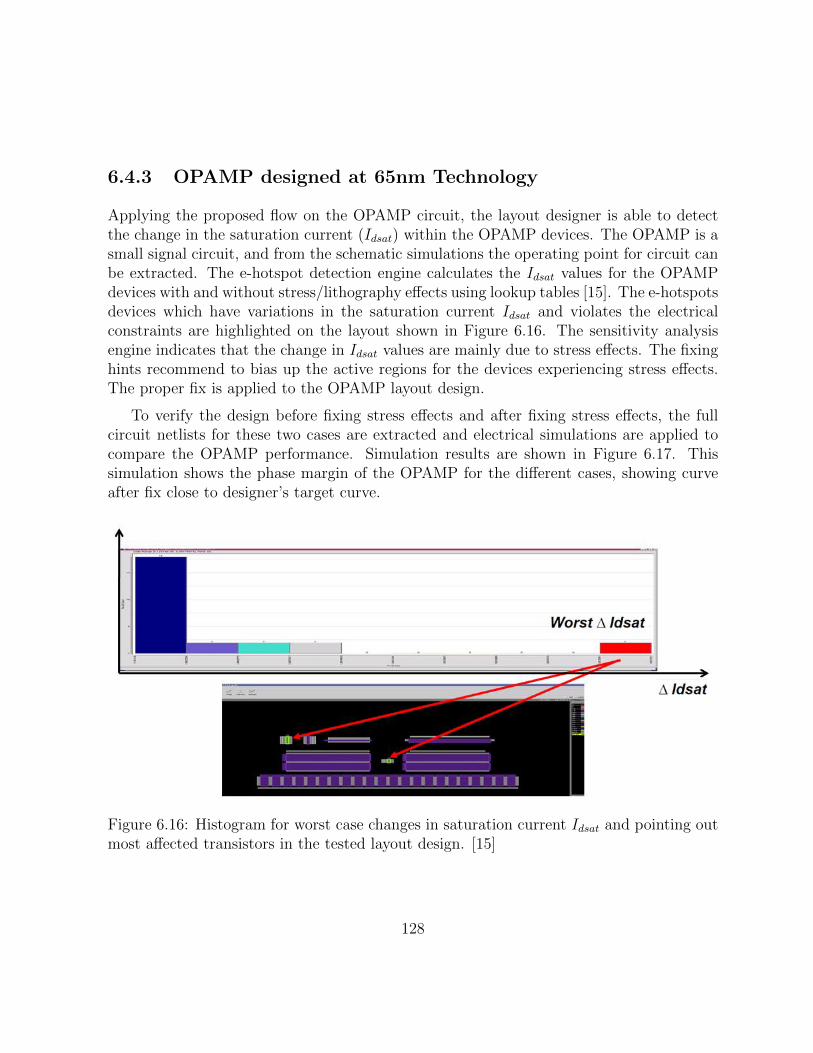
6.4.3 OPAMP designed at 65nm Technology
Applying the proposed flow on the OPAMP circuit, the layout designer is able to detectthe change in the saturation current (Idsat) within the OPAMP devices. The OPAMP is asmall signal circuit, and from the schematic simulations the operating point for circuit canbe extracted. The e-hotspot detection engine calculates the Idsat values for the OPAMPdevices with and without stress/lithography effects using lookup tables [15]. The e-hotspotsdevices which have variations in the saturation current Idsat and violates the electricalconstraints are highlighted on the layout shown in Figure 6.16. The sensitivity analysisengine indicates that the change in Idsat values are mainly due to stress effects. The fixinghints recommend to bias up the active regions for the devices experiencing stress effects.The proper fix is applied to the OPAMP layout design.
To verify the design before fixing stress effects and after fixing stress effects, the fullcircuit netlists for these two cases are extracted and electrical simulations are applied tocompare the OPAMP performance. Simulation results are shown in Figure 6.17. Thissimulation shows the phase margin of the OPAMP for the different cases, showing curveafter fix close to designer’s target curve.
Figure 6.16: Histogram for worst case changes in saturation current Idsat and pointing outmost affected transistors in the tested layout design. [15]
128
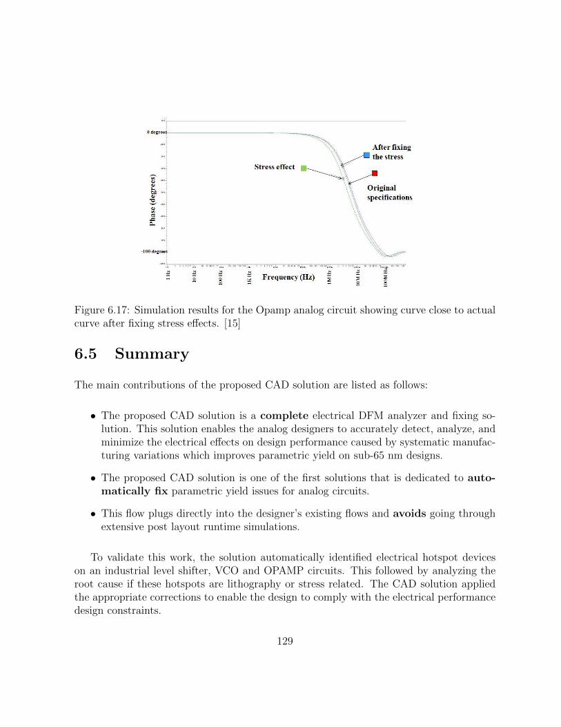
Figure 6.17: Simulation results for the Opamp analog circuit showing curve close to actualcurve after fixing stress effects. [15]
6.5 Summary
The main contributions of the proposed CAD solution are listed as follows:
• The proposed CAD solution is a complete electrical DFM analyzer and fixing so-lution. This solution enables the analog designers to accurately detect, analyze, andminimize the electrical effects on design performance caused by systematic manufac-turing variations which improves parametric yield on sub-65 nm designs.
• The proposed CAD solution is one of the first solutions that is dedicated to auto-matically fix parametric yield issues for analog circuits.
• This flow plugs directly into the designer’s existing flows and avoids going throughextensive post layout runtime simulations.
To validate this work, the solution automatically identified electrical hotspot deviceson an industrial level shifter, VCO and OPAMP circuits. This followed by analyzing theroot cause if these hotspots are lithography or stress related. The CAD solution appliedthe appropriate corrections to enable the design to comply with the electrical performancedesign constraints.
129
Chapter 7
Summary and Conclusions
7.1 Conclusion
As VLSI technology scales to 65nm and below, traditional communication between designand manufacturing becomes more and more inadequate. Gone are the days when designerssimply pass the design tape out file to the foundry and expect very good manufacturingand parametric yield. This is largely due to the enormous challenges in the manufacturingstage as the feature size continues to shrink. Thus, the idea of Design for Manufacturing(DFM) is becoming very popular. Even though there is no universally accepted definitionof DFM, the idea is to convey the manufacturing information into the design stage in away that is understood by designers. Consequently, designers can act on the informationto improve both the manufacturing and parametric yield . In this thesis, different CADsolutions are proposed to provide designers with high performance systematic variationanalysis tools. In addition, these CAD solutions aid the designers with different designenhancement techniques.
At the process variation analysis level, in Chapter 3, we proposed a design context-aware and process-aware methodology to perform a quantitative study of the impact ofsystematic variations for different circuits’ electrical and geometrical behavior. The ex-isting simulation-based process variation analysis solutions face several challenges, mainlythe high computational silicon simulation time. To address this issue, a novel solution isintroduced in Chapter 4 to highly reduce the lithography simulation runtime with a mini-mum impact on accuracy. Another challenge for the existing simulation-based or even thepattern matching-based process variation analysis solution is the lack of the design andelectrical awareness of the circuit. Therefore a high performance electrical driven hotspot
130
detection CAD solution for full chip design was presented in Chapter 5, using a novel deviceparameter matching technique. This solution delivered extraordinary fast and accurate re-sults. Finally a parametric DFM hotspot detection and design driven analysis solutionthat is dedicated for analog circuits, was introduced in Chapter 6. This solution was veri-fied with silicon wafer measurements for a level shifter circuit confirming the existence ofparametric yield issues in the design.
At the design enhancement level, the proposed CAD solutions provide designers withvarious design enhancement and correction methods. For digital designers, a DFM-awarestandard cell re-characterization flow was proposed in Chapter 4 to attain a more robustdigital design. This solution was examined on 45nm FIR chip. For analog designers, anautomated correction solution that is based on systematic variation sensitivity analysiswas devised in Chapter 6. Several analog circuits were used for design enhancement andcorrection experiments.
Hopefully, the proposals in this thesis is to help designers successfully capture, under-stand, and fix manufacturing defects to improve both the manufacturing and parametricyield of a design.
7.2 Summary of Contributions
• Implement four CAD solutions to cover different aspects of the DFM:
– Physical and parametric DFM
– DFM analysis and design enhancement
• These technology independent solutions consider different design types:
– Solutions for digital designs
– Solutions for analog designs
– Experiments on 130nm, 65nm, and 45nm technologies.
• New philosophies were adopted:
– Ultra-fast electrical driven hotspot detection solution based on device parame-ters instead of their geometrical information.
– Fix Before Design CAD solution: DFM-aware Standard Cell re-characterization
131
• Novel CAD engines which were deployed in the industry:
– DFM-aware Smart Device Matching engine (patent pending).
– Intent Driven Design engine (the engine is tested and deployed at On-Semi Corp.and implemented within industrial CAD tools: Calibre PERC LDL MentorGraphics)
• Key features of the proposed CAD solutions:
– Design intent driven solutions, electrical awareness
– RET awareness, design context awareness, lithography and stress awareness
– Fast runtime algorithms and avoid time-consuming simulations
– Provide a complete DFM solution for Analog circuits: Detection-Analysis-Correction
7.3 Future Research Directions
Potential ideas could be added, as future work, to the design intent driven solutions. Onechallenge that can be addressed, is defining electrical constraints. Usually the designersfind electrical constraints is somewhat cumbersome, as they must be able to translate theallowed variations of circuit specifications (for example: gain and bandwidth) to allowedvariations in device parameters. One idea is to develop a tool based on Symbolic Simula-tion [137]. Symbolic simulation involves evaluating circuit behavior using special symbolicvalues to encode a range of circuit operating conditions. In one simulation run, a symbolicsimulator can compute what would require many runs of a traditional simulator. Integrat-ing such function or similar into the design intent driven system could add value to theparametric-aware DFM tools.
132
Appendix A
Appendix: Pending Patents from thisWork
1. Working title of the invention: Novel Technique for DFM-aware Device Match-ing
Short abstract of the invention: For technology nodes of 45nm and below; advanceddevice parameters extracted from the layout can have a significant effect on the onthe results of the electrical simulations. Running full chip electrical simulation can beone way to accurately predict the behavior of the devices taking into account layouteffects. However this approach is time consuming. In proposed method the devicesthat have their corresponding parameter values within a given tolerance are groupedtogether. The effect of the these parameters on the electrical simulations is the samefor all the devices in the same group, thus grouping layout devices into sets of uniquedevices, in respect to these parameters, can greatly reduce the simulation time bysimulating the unique devices only and mapping the electrical variation to the restof the design devices.
2. Working title of the invention: Electrical Driven Process Variations Checks
Short abstract of the invention: As IC design became a more complex process, thedesigner now not only takes care of the normal design and layout parameters as usual,but also needs to consider the process variation impact on his design to preserve thesame chip functionality with no failure during fabrication. In the current process;schematic designers go through extensive simulations to cover all the possible vari-ations on their design parameters and hence on the design functionality. At the
133

same time layout designers perform a time consuming simulations such as lithogra-phy simulations, chemical mechanical polishing simulations (CMP), critical featureanalysis and then perform lithography/stress verification checks on the complete lay-out which is also time consuming that impacts the design turn-around-time. Ournovel methodology provides a fully automated CAD flow that captures the designersprocess constraints from the schematic netlist; then define a prioritized list of the pro-cess sensitive devices and nets, that are then automatically linked and highlighted onthe physical layout level; then followed by running verification checks using CalibreDFM, LFD suite tools avoiding the time consuming full chip simulations .
3. Working title of the invention: A Parametric DFM Solution for Analog Cir-cuits: Electrical Driven Hot Spot Detection, Analysis and CorrectionFlow
Short abstract of the invention: Recently, there has been an increased emphasis onparametric yield issues, referred to as electrical-DFM (e-DFM). In this invention, wepresent the only (up to our knowledge) complete electrical-driven design for manu-facturing solution that detects, analyzes, and automatically fixes electrical hotspots(e-hotspots) caused by different process variations within the analog circuit design.Our proposed flow is examined on a 130nm, 65nm, and 45nm industrial analog cir-cuits.
134
References
[1] A. Sreedhar, “Automatic techniques for modeling impact of sub-wavelength lithog-raphy on transistors and interconnects and strategies for testing lithography induceddefects,” Ph.D. dissertation, University of Massachusetts Amherst, 2008. xii, 1, 2
[2] P. Sharma, “Manufacturing-aware physical design techniques,” Ph.D. dissertation,University of California, San Diego, 2007. xii, 9, 11, 13
[3] B. Lee, “Modeling of chemical mechanical polishing for shallow trench isolation,”Ph.D. dissertation, Massachusetts Institute of Technology, 2002. xii, 15, 22, 31
[4] M. H. Abu-Rahma, “Design of variation-tolerant circuits for nanometer CMOS tech-nology: Circuits and architecture co-design,” Ph.D. dissertation, University of Wa-terloo, 2008. xii, 8, 15, 21
[5] P. G. Drennan, M. L. Kniffin, and D. R. Locascio, “Implications of proximity effectsfor analog design,” Custom Integrated Circuits Conference, pp. 169 – 176, 2006. xii,16, 17, 25, 113
[6] D. Abercrombie, P. Elakkumanan, and L. Liebmann, “Restrictive design rules andtheir impact on 22 nm design and physical verification,” Mentor Graphics TechnicalLibrary, 2009. xii, 20
[7] N. Verghese and P. Hurat, “DFM reality in sub-nanometer IC design,” Design Au-tomation Conference (ASP-DAC), 2007 16th Asia and South Pacific, 2007. xii, 21,22
[8] N. S. Nagaraj, T. Bonifield, A. Singh, U. N. Frank Cano, M. Kulkarni, P. T. Balsara,and C. D. Cantrell, “Benchmarks for interconnect parasitic resistance and capaci-tance,” ISQED, 2003. xii, 24
135
[9] Y. Cheng and C. Hu, MOSFET Modeling and BSIM User Guide. Kluwer AcademicPublishers. xii, xiv, 19, 23, 24, 89, 90, 113, 114
[10] C. Mack, “Modeling solvent effects in optical lithography,” Ph.D. dissertation, Uni-versity of Texas at Austin, 1998. xii, 32, 33
[11] Calibre Workbench Manual. Mentor Graphics Corp. xii, 42, 43
[12] T. Ma, “Improving design quality by managing process variability,” ISQED, 2009.xii, xiv, 43, 86
[13] Tsien, “Context-specific leakage and delay analysis of a 65nm standard cell libraryfor lithography-induced variability,” Proceedings of SPIE 6521, 65210F, 2007. xiii,44, 49, 50, 51, 61
[14] R. Martins, “On the design of very low power integrated circuits,” Ph.D. dissertation,Swiss Academy of Engineering Science, 1998. xiii, 56
[15] H. M. Eissa and A. E. ElMously, “Physical aware design methodology for analog andmixed signal integrated circuits,” IEEE International Design and Test Workshop(IDT), 2009. xiv, xv, 104, 112, 113, 128, 129
[16] W. Evans and D. Burnell, “Deep submicron effects on data converter buildingblocks,” IEEE Custom Intergrated Circuits Conference (CICC), 2008. xiv, 111
[17] C. Robertson, “E-DFM: The future of parametric yield success,” Chip Design: Tools,Technologies and Methodologies. 1, 102
[18] S. Nassif, “Design for variability in DSM technologies,” In Proceedings of First In-ternational Symposium on Quality of Electronic Design, p. 451454, 2000. 1
[19] S. Borkar, “Designing reliable systems from unreliable components: The challengesof transistor variability and degradation,” IEEE Micro, 2005. 1
[20] K. Harris, “The next generation of DFM tools: Die-level parametric variation mon-itoring,” ChipEstimate.com, 2011. 1
[21] W. Poppe and L. Capodieci, “Platform for collaborative DFM,” Proc. SPIE Int. Soc.Opt. Eng 6156,124, 2006. 2
[22] S. Borkar, T. Karnik, S. Narendra, J. Tschanz, A. Keshavarzi, and V. De, “Parametervariations and impact on circuit and microarchitecture,” IEEE Micro, pp. 30–39,2006. 7
136

[23] B. Wong, A. Mittal, Y. Cao, and G. W. Starr, “Nano-CMOS circuit and physicaldesign,” Wiley-Interscience, 2004. 8, 9
[24] A. Chandrakasan, W. J. Bowhill, and F. Fox, “Design of high-performance micro-processor circuits,” Wiley-IEEE Press, 2000. 8, 9
[25] A. Srivastava, D. Sylvester, and D. Blaauw, “Statistical analysis and optimizationfor VLSI: Timing and power (series on integrated circuits and systems),” Springer,2005. 8, 9
[26] H. Masuda, S. Ohkawa, A. Kurokawa, and M. Aoki, “Challenge: variability charac-terization and modeling for 65- to 90-nm processes,” Proceedings of IEEE CustomIntegrated Circuits conference, pp. 593–599, 2005. 8
[27] S. Borkar, T. Karnik, S. Narendra, J. Tschanz, A. Keshavarzi, and V. De, “Parametervariations and impact on circuits and microarchitecture,” Proceedings of the 40thconference on Design automation, pp. 338–342, 2003. 8
[28] K. Bowman, S. Duvall, and J. Meindl, “Impact of die-to-die and within-die parameterfluctuations on the maximum clock frequency distribution for gigascale integration,”IEEE Journal of Solid-State Circuits, pp. 183–190, 2002. 8
[29] H. J. Levinson, Mircolithography: Science and Technology. SPIE The InternationalSociety of Optical Engineering, 2001. 9, 11, 19
[30] A. K.-K. Wong, Resolution Enhancement Techniques in Optical Lithography. SPIEThe International Society of Optical Engineering, 2001. 11
[31] J. R. Sheats and B. W. Smith, Principles of Lithography. Marcell Dekker, 1998. 14
[32] B. Lee, D. S. Boning, D. L. Hetherington, and D. J. Stein, “Using smart dummy filland selective reverse etchback for pattern density equalization,” Chemical-MechanicalPolish for VLSI/ULSI Multilevel Interconnection Conference, pp. 255–258, 2000. 14
[33] B. Stine, D. Ouma, R. Divecha, D. S. Boning, J. Chung, D. Hertherington, C. R.Harwood, O. S. Nakagawa, and S.-Y. Oh, “Rapid characterization and modeling ofpattern dependent variation in chemical-mechanical polishing,” in IEEE Trans. onSemiconductor Manufacturing, pp. 129–140, 1998. 15
[34] T. Tugbawa, “Chip-scale modeling of pattern dependencies in copper chemical me-chanical polishing processes,” Ph.D. dissertation, Massachusetts Institute of Tech-nology, 2002. 15, 22, 31
137
[35] A. Kahng, G. Robins, H. W. A. Singh, and A. Zelikovsky, “Filling and slotting: Anal-ysis and Algorithms,” in Proc. IEEE International Symposium on Physical Design,1998, pp. 95–102, 1998. 15
[36] K. W. Su and et al., “A scaleable model for STI mechanical stress effect on layoutdependence of MOS electrical characterization,” IEEE CICC, pp. 245–248, 2003. 17,23
[37] R. A. Bianchi, G. Bouche, and O. R. dit Buisson, “Accurate modeling of trench iso-lation induced mechanical stress effects on MOSFET electrical performance,” IEDMTech. Dig, pp. 117–120, 2002. 17, 23, 38
[38] T. Hook and et al., “The dependence of channel length on channel width in narrow-channel CMOS devices for 0.25-0.13 um technologies,” IEEE Electron Device Letters,pp. 85–87, 2000. 17
[39] G. Scott and et al., “NMOS drive current reduction caused by transistor layout andtrench isolation induced stress,” IEEE IEDM, pp. 827–830, 1999. 17
[40] T. R. Hook, J. Brown, and X. Tian, “Proximity effects and VLSI design,” ICICT,pp. 167–170, 2005. 17, 18, 25
[41] M. Miyamoto and et al., “Impact of reducing STI-induced stress on layout depen-dence of MOSFET characteristics,” IEEE Trans. Elec. Dev., pp. 440–443, 2004. 17
[42] S. Wolf, “Silicon processing for the VLSI era,” Process Integration, p. 389, 2004. 18
[43] T. B. Hook and et al., “Lateral ion implant straggle and mask proximity effect,”IEEE Trans. Elec. Dev., pp. 1946–1951, 2003. 18, 25
[44] S. Postnikove and S. Hector, “CD error budgets: Proposed simulation study method-ology,” ITRS, 2003. 19
[45] A. Wong, R. Ferguson, L. Liebmann, S. Mansfield, A. Molless, and M. Neisser,“Lithographic effects of mask critical dimension error,” SPIE Conference on OpticalMicrolithography, pp. 106 – 116, 1998. 19
[46] T. Brunner, “Impact of lens aberrations on optical lithography,” IBM Journal ofResearch and Development, 1997. 19
138
[47] A. Bourov, L. C. Litt, and L. Zavyalova, “Impact of flare on CD variation for 248nmand 193nm lithography systems,” SPIE Conference on Optical Microlithography, p.1388 393, 2001. 19
[48] C. Hedlund, H.-O. Blom, and S. Berg, “Microloading effect in reactive ion etching,”Journal of Vacuum Science and Technology, pp. 1962–1965, 1994. 19
[49] S. Nassif, “Modeling and analysis of manufacturing variations,” IEEE Pmc. Of CICC,pp. 223–228, 2001. 22
[50] R. Arunachaiam, K. Rajagopal, and L. T. Pileggi, “TACO: Timing analysis withcoupling,” In Proc. Design Automation Conf., 2000. 23
[51] D. Wu, J. Hu, and R. Mahapatra, “Coupling aware timing optimization and antennaavoidance in layer assignment,” In Proc. Int. Symp. on Physical Design, 2005. 23
[52] D. Wu, J. Hu, M. Zhao, and R. Mahapatra, “Timing driven track routing consideringcoupling capacitance,” In Proc. Asia and South Pacific Design Automation Conf.,2005. 23
[53] M. Cho and D. Z. Pan, “Wire density driven global routing for CMP variation andtiming,” ICCAD, 2006. 23
[54] H. S. L. et al., “An optimized densification of the filled oxide for quarter micronshallow trench isolation (STI),” IEEE Symposium on VLSI Technology, pp. 158–159,1996. 25
[55] V. Moroz, L. Smith, X. Lin, D. Pramanik, and G. Rollins, “Stress-aware designmethodology,” IEEE International Symposium on Quality Electronic Design, pp.807–812, 2006. 25
[56] L. W. L. et al., “High-performance circuit design for the RET enabled 65-nm technol-ogy node,” SPIE Conference on Design and Process Integration for MicroelectronicManufacturing, pp. 20–29, 2004. 28
[57] C. Visweswariah, “Death, taxes and failing chips,” ACM/IEEE Design AutomationConference, pp. 343 – 347, 2003. 28
[58] I. A. Wagner and I. Koren, “An interactive VLSI CAD tool for yield estimation,”IEEE Trans. on Semiconductor Manufacturing, 1995. 29
139

[59] S. Nojima, S. Mimotogi, M. Itoh, O. Ikenaga, S. Hasebe, K. Hashimoto, S. Inoue,M. Goto, and I. Mori, “Flexible mask specifications,” SPIE BACUS Symposium onPhotomask Technology, pp. 187–196, 2002. 29
[60] A. Kahng, G. Robins, A. Singh, , and A. Zelikovsky, “Filling algorithms and analysesfor layout density control,” IEEE Trans. on Computer-Aided Design of IntegratedCircuits and Systems, pp. 445–462, 1999. 31
[61] M. Fujinaga, N. Kotani, T. Kunikiyo, H. Oda, M. Shirahata, and Y. Akasaka, “Three-dimensional topography simulation model: Etching and lithography,” IEEE Trans-actions on Electron Devices, 1990. 32, 34
[62] G. Nicosia, S. Rinaudo, and E. Sciacca, “An evolutionary algorithm-based ap-proach to robust analog circuit design using constrained multiobjective optimiza-tion,” Knowledge-Based Syst, pp. 175–183, 2008. 35
[63] M. Jack, D. Ertugrul, and O. Edward, “US20080005717,” US Patent, 2008. 35
[64] S. Mansfield, L. Liebmann, A. Krasnoperova, and I. Grauer, “US20070261013,” USPatent, 2007. 35
[65] T. Steven and J. Etienne, “US20077117468,” US Patent, 2007. 35
[66] V. Ramnath, C. Ruggero, and R. Subramanian, “US20080013383,” US Patent, 2008.35
[67] L. Chih-Ming, L. Ru-Gun, S. I-Chang, K. Yao-Ching, and H. Cliff, “US20070266362,”US Patent, 2007. 35
[68] H. Katsuhiko, “US20080003510,” US Patent, 2008. 35
[69] L. Mu-Jing, “US20070300195,” US Patent, 2007. 35
[70] D. Kevin, E. Robert, D. Mehul, J. Kirk, Y. Chimin, and T. Jason, “US20077284231,”US Patent, 2007. 35
[71] F. Fiorante, G. Nicosia, S. Rinaudo, and G. Stracquadanio, “Automatic layout op-timization of power mosfets using innovative distributed model technique,” IEEEInternational Symposium on Industrial Electronics ISIE, 2008. 35
[72] S. Abdurrahman, “US20077266800,” US Patent, 2007. 35
140
[73] W. Ting-Chi and L. Kuang-Yao, “US20077302662,” US Patent, 2007. 35
[74] W. Hung-Sheng, T. Hui-Kuo, H. Chi-Yen, Y. Chi-Kuen, and M. DinGuow,“US20070277132,” US Patent, 2007. 35
[75] V. Moroz, X. Xu, D. Pramanik, F. Nouri, and Z. Krivokapic, “Analyzing strained-silicon options for stress-engineering transistors,” Solid State Technology, pp. 49–50,52, July 2004. 38
[76] S.-M. Bae, H.-E. Kim, Y.-M. Ham, S.-C. Moon, , and S.-H. Choi, “Quantitativeanalysis of the proximity effect in optical lithographic process,” Proc. SPIE, Vol.2196, 254, 1994. 38, 42
[77] Cadence, “Increasing parametric yield,” White Paper. 39
[78] B. Stine, D. Boning, J. Chung, D. Ciplickas, and J. Kibarian, “Simulating the impactof poly CD wafer-level and die-level variation on circuit performance,” InternationalWorkshop on Statistical Metrology, pp. 24–27, 1997. 39
[79] R. Salem, H. AbdelGhany, A. Elmously, H. Eissa, and M. Anis, “Implementing amethodology for process variation awareness of design context and its impact oncircuit analysis,” IEEE International Design and Test Workshop (IDT),, November2009. 42
[80] A. B. Kahng, P. Sharma, and R. O. Topaloglu, “Exploiting STI stress for perfor-mance,” Proc. 2007 IEEE/ACM International Conference on Computer-aided de-sign, pp. 83–90, 2007. 43, 113
[81] R. Fathy, H. AbdelGhany, A. R. ElMously, H. Eissa, and M. Anis, “Implementinga methodology for process variation awareness of design context and its impact oncircuit analysis,” 4th IEEE International Design and Test workshop IDT, 2009. 44
[82] K. Cao, J. Hu, and S. Dobre, “Standard cell characterization considering lithographyinduced variations,” Qualcomm, Inc, San Diego, CA. Dept. of Electrical EngineeringTexas A&M University College Station, TX presented at DAC, 2006. 48, 61, 74
[83] M. Al-Imam, A. Torres, J.-M. Brunet, M. Fakhry, and R. Fathy, “Optimization ofprocess window simulations for litho friendly design frame work,” BACUS, 2006. 51
[84] W. J. Poppe, L. Capodieci, J. Wu, , and A. Neureuther, “From poly line to transistor:Building bsim models for non-rectangular transistors,” spie, 2006. 51, 110
141
[85] S. X. Shi, P. Yu, and D. Z. Pan, “A unified non-rectangular device and circuitsimulation model for timing and power.” 51
[86] J. Rabaey and A. Chandrakasan, Digital Integrated Circuits, A Design Prospective.Second Edition. 52
[87] R. Fathy, A. ElMousley, H. Eissa, M. Dessouky, and M. Anis, “A DFM tool for ana-lyzing lithography and stress effects on standard cells and critical path performancein 45nm digital designs,” 5th IEEE International Design and Test workshop IDT,2010. 52
[88] R. Fathy, M. Al-Imam, H. Diab, M. Fakhry, J. Torres, B. Graupp, J. M.Brunet,and M. Bahnas, “Litho aware method for circuit timing/power analysis through pro-cess,” Proc. VOLUME=6521 Design for Manufacturability through Design-ProcessIntegration, SPIE Advanced Lithography, 2007. 55
[89] G. A. Gomba, “Collaborative innovation: IBMs immersion lithography strategy for65 nm and 45 nm half-pitch nodes & beyond,” SPIE Conference on Optical Mi-crolithography, 2007. 60
[90] J.Wiley, “Future challenges in computational lithography (cover story),” Solid StateTechnology, p. 68, 2006. 60
[91] C. Albertalli and T. Kingsley, “Computational lithography (cover story),” Semicond.Int., pp. 36–42, 2007. 60
[92] T. Kingsley, J. Sturtevant, S. McPherson, and M. Sexton, “Advances in computehardware platforms for computational lithography,” SPIE, 2007. 60
[93] S. Suh, S. Lee, K.-Y. Back, S. Lee, Y. Kim, S. Kim, and Y.-J. Chun, “Three-dimensional mask effect approximate modeling for sub-50-nm node device OPC,”SPIE, 2007. 60
[94] J. Yang, L. Capodieci, and D. Sylvester, “Advanced timing analysis based on post-OPC extraction of critical dimensions,” DAC, pp. 359–364, 2005. 60
[95] P. Gupta, A. Kahng, D. Sylvester, , and J. Yang, “Performance-driven OPC for maskcost reduction,” CM/IEEE International Symposium on Quality Electronic Design,pp. 270–275, 2005. 62, 85
142

[96] R. Fathy and M. Anis, “An automated methodology for implementing a DFM-awarestandard cell library under process window and context variations,” 8th IEEE Inter-national NEWCAS Conference, 2010. 62
[97] J. A. Torres and C. N. Berglund, “Integrated circuit DFM framework for deep sub-wavelength processes,” Proc. SPIE Int. Soc. Opt. Eng. 5756, 39, 2005. 62, 73
[98] J. A. Torres and F. Pikus, “Unified process-aware system for circuit layout verifica-tion,” Proc. SPIE Int. Soc. Opt. Eng. Volume 6521, p. 652108, 2007. 62
[99] J. A. Torres and N. Cobb, “Study towards model-based DRC verification,” SPIEConference on Optical Microlithography, 2005. 64, 70
[100] A. Krasnoperova, J. A. Culp, I. Graur, S. Mansfield, M. Al-Imam, and H. Maaty,“Process window OPC for reduced process variability and enhanced yield,” SPIEConference on Optical Microlithography, 2006. 70
[101] J. Word and K. Sakajiri, “OPC to improve lithographic process window,” SPIEConference on Optical Microlithography, 2006. 70
[102] J. A. Torres, T. Roessler, and Y. Granik, “Process window modeling using compactmodels,” SPIE Conference on Optical Microlithography, 2004. 70
[103] S. Mansfield, G. Han, M. Al-Imam, and R. Fathy, “Through-process modeling in aDfM environment,” SPIE Conference on Optical Microlithography, 2006. 70
[104] E. Chin, C. Levy, , and A. R. Neureuther, “Variability aware timing models at thestandard cell level,” Design for Manufacturability through Design-Process Integration,SPIE Advanced Lithography, 2010. 80
[105] H. Yao, S. Sinha, and et al., “Efficient process-hotspot detection using range pat-tern modeling,” Proceedings of the 2006 IEEE/ACM International Conference onComputer-Aided Design, pp. 625–632, 2006. 83, 84
[106] P. Brooker, H. Koop, and H. Marquardt, “Using DFM hot-spot analysis for predictingresist patterns,” Solid State Technology, pp. 47–49, 2005. 84
[107] J. K. et al., “Hotspot detection on post-opc layout using full chip simulation basedberification tool: A case study with aerial image simulation,” SPIE, 2003. 84
[108] E. R. et al., “Automated full-chip hotspot detection and removal flow for interconnectlayers of cell-based designs,” SPIE, 2007. 84
143

[109] M. Ma, M. Anderson, and et al., “A novel approach for hot-spot removal for sub-100nm manufacturing,” SPIE, 2006. 84
[110] S. Kyoh, T. Kotani, and et al., “Lithography oriented DfM for 65nm and beyond,”SPIE, 2006. 84
[111] F. Gennari, G. Robins, and A. Neureuther, “Validation of the aberration pattern-matching OPC strategy,” SPIE, pp. 444–453, 2003. 84
[112] A. Kahng and et.al, “DFM: Where’s the proof of value?” DAC, 2006. 85, 105, 106
[113] D. Ding, X. Wu, J. Ghosh, and D. Z. Pan, “Machine learning based lithographichotspot detection with critical feature extraction and classffication,” ICICDT Conf.,2009. 85, 100
[114] D. Reed, “Electrical-DFM: Focusing on what matters to chip designers,” Chip De-sign: Tools, Technologies and Methodologies. 85, 102
[115] J. Segura, A. Keshavarzi, J. Soden, and C. Hawkins, “Parametric failures in CMOSICs: A defect-based analysis,” Proceedings of the 2002 IEEE International Test Con-ference, 2002. 85, 102
[116] S. Banerjee, P. Elakkumanan, L. Liebmann, J. C. M., and Orshansky, “Electricallydriven optical proximity correction,” SPIE, 2008. 85
[117] B. Yongchan, S. Sundareswaran, and D. Pan, “Total sensitivity based DFM opti-mization of standard library cells,” Proceedings of the 19th international symposiumon Physical design, pp. 113–120, 2010. 85
[118] S. Bhattacharya, N. Jangkrajamg, R. Hartono, and C.-J. R. Shi, “Hierarchical ex-traction and verification of symmetry constraints for analog layout automation,” Asiaand South Pacific Design Automation Conference, 2004. 87
[119] R. Fathy, M. Al-Imam, A. Arafa, A. ElMousley, H. Eissa, and M. Anis, “High per-formance electrical driven hotspot detection CAD solution for full chip design usinga novel device parameter matching technique,” 2011, unpublished. 87
[120] Calibre Verification User Manual. Mentor Graphics Corp. 91, 94, 95
[121] Calibre Designrev Reference Manual. Mentor Graphics Corp. 94, 95
144
[122] A. Arafa, H. Wagieh, R. Fathy, J. F. D. Morgan, M. Dessouky, and M. Anis,“Schematic-driven physical verification: Fully automated solution for analog IC de-sign,” 48th Design Automation Conference User Track, 2011. 95
[123] D. Ding, A. J. Torres, F. G. Pikus, and D. Z. Pan, “High performance lithographichotspot detection using hierarchically refined machine learning,” Design AutomationConference (ASP-DAC), 2011 16th Asia and South Pacific, 2011. 100
[124] D. G. Drmanac, F. Liu, and L. Wang, “Predicting variability in nanoscale lithographyprocesses,” Design Automation Conf., 2009. 100
[125] A. J. Torres, M. Hofmann, , and O. Otto, “Directional 2D functions as models forfast layout pattern transfer verification,” SPIE, 2009. 100
[126] L. Lewyn, “Physical design and reliability issues in nanoscale analog cmos technolo-gies,” NORCHIP, pp. 1–10, 2009. 104, 111
[127] B. Wang, H. Nguyen, J. Mavoon, A. Horch, Y. Ma, T. Humes, and R. Paulsen,“Effect of layout orientation on the performance and reliability of high voltage N-LDMUS in standard submicron logic STI CMOS process,” 2005. 104
[128] P. Gupta and F. Heng, “Toward a systematic-variation aware timing methodology,”DAC, pp. 321–326, 2004. 106
[129] P. Gupta, B. Khang, and D. Sylvester, “Self-compensating design for focus variation,”DAC, pp. 365–368, 2005. 106
[130] A. Kahng, “Key directions and a roadmap for electrical design for manufacturability,”Solid State Circuits Conference, pp. 83 – 88, 2007. 106
[131] R. Fathy, A. Arafa, S. Hany, A. ElMousley, H. Eissa, D. Nairn, and M. Anis, “Aparametric DFM CAD solution for analog circuits: Electrical driven hot spot detec-tion, analysis and correction flow,” 24th IEEE International SOC Conference, 2011.107
[132] S. Hammouda, H. Said, M. Dessouky, M. Tawfik, Q. Nguyen, W. Badawy, H. Abbas,and H. Shahein, “Chameleon ART: a non-optimization based analog design migrationframework,” Proceedings of the 43rd annual Design Automation Conference, 2006.108, 116
145

[133] R. Salem, H. AbdelGhany, , and M. Anis, “An automated methodology for im-plementing a DFM-aware standard cell library under process window and contextvariations,” 8th IEEE International NEWCAS Conference, July 2010. 110
[134] A. Azuma, A. Oish, Y. Okayama, K. Kasai, and Y. Toyoshima, “Methodology ofMOSFET characteristics flutuations description using BSIM3v3 SPICE model forstatistical circuit siluations,” Int’l Workshop on Statistical Metrology Technical Pa-pers, 1998. 113
[135] P. B. Y. Tan, A. Kordesch, and O. Sidek, “Effect of shallow trench isolation inducedstress on CMOS transistor mismatch,” IEEE International Conference ICSE, 2004.113
[136] S. Hany and M. Dessouky, “Operating point extraction techniques,” 2011, unpub-lished. 125
[137] G. Gielen, H. Walscharts, and W. Sansen, “ISAAC: A symbolic simulator for analogintegrated circuits,” IEEE Journal of Solid-State Circuits, VOL. 24, NO, 6, 1989.132
146