Embed Size (px)
Citation preview
Electrical Transport in Schottky Barrier MOSFETs
A DissertationPresented to the Faculty of the Graduate School
of Yale University
in Candidacy for the Degree ofDoctor of Philosophy
by
Laurie Ellen Calvet
May 2001
Electrical Transport in Schottky Barrier MOSFETs
A DissertationPresented to the Faculty of the Graduate School
of Yale University
in Candidacy for the Degree ofDoctor of Philosophy
by
Laurie Ellen Calvet
Dissertation Director: Professor Mark A. Reed
May 2001

Abstract
Electrical Transport in Schottky Barrier MOSFETs
Laurie Ellen Calvet
Yale University
2001
The motivation for this thesis originates in the semiconductor industry whose rapid
economic growth in the past thirty years has been stimulated by scaling transistors to
smaller dimensions. The current drive to design transistors beyond fundamental
limitations is causing the industry to consider alternative structures. The Schottky Barrier
(SB) MOSFET is one such device. It consists of metallic silicide source and drain
contacts and a standard MOS gate. Previously, simulations have indicated that these
transistors will have superior scaling properties and be more cost effective to fabricate
than conventional transistors when channel lengths are scaled below 70 nm. This
research experimentally investigates the current transport and scaling behavior of
pSBMOSFETs fabricated on bulk silicon substrates.
We also explore the unique low temperature properties of Schottky Barrier (SB)
MOSFETs. We find evidence that single charged impurities cause ‘hot spots’ that result
in a reduced local potential at the abrupt metal/semiconductor interface. At relatively
high temperatures (20-100 K) the impurities give rise to a non-uniform Schottky Barrier

height. At lower temperatures electrons crossing the ~ 8 nm barrier width are coherent,
and a single impurity causes both enhanced direct tunneling and a resonant state due to
the confined potential. As a result, we observe quantum interference between these two
distinct paths of a single electron, known as a Fano resonance. Tuning of the interference
is explored by varying temperature, bias direction and bias magnitude.

© Copyright by Laurie Ellen Calvet 2001 All Rights Reserved

i
Contents
Acknowledgements iii
List of Figures v
List of Tables ix
List of Abbreviations and Symbols x
Chapter 1. Introduction 1 1.1. Why study the SBMOSFET? 1 1.2. Introduction to the SBMOSFET 4 1.3. The SBMOSFET at Cryogenic Temperatures 8 1.4. Previous Work 11
1.4.A. Device Physics 11 1.4.B. Fano Resonances 12
Chapter 2. Background 17 2.1. The Schottky Barrier: Electrostatics and Applied Bias 17 2.2. Transport Mechanisms 23
2.2.A. Transport Over the Barrier 26 2.2.B. Field and Thermionic Field Emission 30
2.3. The MOS Capacitor 34 2.4. The Conventional MOSFET 41 2.5. MOSFETs at Cryogenic Temperatures 44 2.6. Resonant Tunneling Through Impurities 47
2.6.A. Landauer Formalism and Resonant Tunneling 48 2.6.B. Previous Research on Localized States 50
Chapter 3. Devices: Fabrication and Experimental Details 53 3.1. Fabrication 53 3.2. Device Layout 55 3.3. Experimental 58
Chapter 4. Device Operation 61 4.1. Simple Circuit Model 61

ii
4.2. Band Bending at the Metal/Semiconductor Interface 66 4.3. Current Transport Limits 69 4.4. Sub-threshold Regime 72 4.5. Device Behavior in the ‘On’ State 78 4.6. Anomalous Leakage Current 85 4.7. Concluding Remarks 90
Chapter 5. Scaling of the SBMOSFET 92 5.1. Definition of Scaling Regimes 93 5.2. Comparison with Experiments 97
Chapter 6. Low Temperature Characteristics 102
6.1. Thermionic Field Emission vs. Field Emission 103 6.2. Field Emission at Low Temperatures 106 6.3. Effect of an Impurity Potential on a Schottky Barrier 110 6.4. Origin of Acceptor Impurities 113 6.5. Transport Through Localized States 115
Chapter 7. Fano Resonances 122
7.1. Theory of Fano Resonances 123 7.2. Evidence of Fano Resonances 126 7.3. Abruptness of the Metal/Semiconductor Interface and Consequences 129 7.4. Temperature Dependence 134 7.5. Bias Dependence 137
Chapter 8. Conclusions 144 Bibliography 148 Appendix A: Quad Layouts and Run Sheet 157 Appendix B: Thermionic Field and Field Emission Details 162

iii
Acknowledgements
For Laurent
First and foremost I would like to thank my advisor Mark Reed for invaluable guidance
throughout my thesis, financial support, constant encouragement and allowing me to
pursue research on SBMOSFETs. I am very grateful to Robert Wheeler; without his
continued help throughout my graduate years and numerous interventions on my behalf
this thesis would not be. Even after his retirement, Bob has always been around to talk to
about physics and his intuition and insights have been immensely helpful. I also thank
T.P. Ma for innumerable discussions and the use of his lab for many different
measurements. In addition, I am grateful to Dan Prober for serving on my thesis
committee, helping me arrange measurements in 408, and numerous helpful discussions.
I thank John Tucker for serving as my outside reader, providing insights into
SBMOSFETs and arranging to have devices sent to me. I am indebted to Chinlee Wang,
his graduate student for invaluable discussions and support. Chinlee and John Snyder
fabricated the wafers used in this research and I am indebted to them for being able to
work on this topic. I also thank Mark Lundstrom for agreeing to be an additional outside
reader for my thesis, especially at such a late date. Finally, I also thank the Advanced
Silicon Technology group at MIT Lincoln Lab, where I had a summer internship during
my fourth year. Not only did I gain invaluable knowledge about SOI technology, I also
discovered new directions for my thesis research through discussions with group
members.
iv
I am indebted to Mandar Deshpande and Chongwu Zhou who trained me for the
SEM, electron beam lithography, and the clean room and prepared me for working in
Mark’s lab. Without Alex Kozhevnikov I would not have learned to wire bond and run
the 4th floor magnet. In addition the numerous discussions about research and physics
have been both helpful and a lot of fun. I am indebted to Andrew Poon and Konrad
Lehnert for numerous discussions about physics, measurements and Fano resonances.
During my last year at Yale, both Andrew and Konrad were always around to help out;
either by lending either a helping hand in experiments or an insightful ear for discussions.
Without them, the Fano resonance work would not have gotten as far as it did. I also
thank Hauke Luebben for support with data acquisition, numerous experiments and data
analysis during my fourth year. I acknowledge and thank the other group members for
discussions and support: Jia Chen, Gabel Chong, James Klemic, Takhee Lee, Jie Su and
Wenyong Wang. I am grateful to Mariangela Lisanti whose enthusiasm reminded me
why I was excited about physics. Finally I thank numerous other people at Yale for
various support, discussions and experimental guidance: Luigi Freznio, Xin Gu, Jin-ping
Han, Xia Hong, Wye-Kye Li, Ashot Melik-, Nathan Rex, Ken Seagall, Ying Shi, Irfan
Siddiqi, Xiewen Wang, and Chris Wilson.
I am very grateful to my family. My husband, parents, Uncle Mel and brothers
have been very supportive about my decision to pursue a Ph.D. Without my Mom’s
undying support I would have never made it this far. My Uncle’s knowledge of research,
the academic world and his quiet pride in my career choice were also invaluable. Finally
I thank my husband whose undying belief that I could finish, endless moral support and
love have been a constant and a comfort throughout my years at Yale.

v
List of Figures page
1-1 Schematic of the SBMOSFET 4
1-2 Device characteristics of a long channel SBMOSFET 6
1-3 Band diagrams of the different operating regimes of the SBMOSFET 7
1-4 Device characteristics at low temperatures 9
1-5 Example of resonance structure and fit to the Fano form 10
2-1 Schematic of an idealized metal/semiconductor contact 19
2-2 Comparison of quasi Fermi levels in diffusion and thermionic emission 23
2-3 Schematic of the band bending with thermionic emission transport 25
2-4 Band diagrams indicating the different energies associated with
thermionic field emission and direct tunneling 30
2-5 Schematic of band diagrams for tunneling 32
2-6 Schematic of the relative energy levels of a separated MOS system 35
2-7 Different regimes of a pMOS capacitor under negative bias 36
2-8 Surface potential vs. gate voltage of a pMOS capacitor at 100 K, 40
200 K and 300 K
2-9 Hole surface concentrations vs. gate voltage at 100 K, 200 K, 300 K 40
2-10 Schematic of a conventional MOSFET 41
2-11 Example of Lorentzian lineshape 50
vi
3-1 SEM micrograph of a long channel device 56
3-2 SEM micrograph close-up of a long channel device. 56
3-3 SEM micrograph of the smallest device in Quad E22 of SBTT25. 57
3-4 XTEM of a small device on NTB11. 57
4-1 Equilibrium band diagram of a SBMOSFET and effective circuit diagram 62
4-2 Is vs Vd characteristics of a pSBMOSFET on a p-type wafer at different 65
temperatures
4-3 Surface concentrations obtained from Silvaco simulator and method of 67
Chapter 2
4-4 Band diagrams of a PtSi/n-type Si/PtSi MSM structure at Vg = 0 68
4-5 Limits of current transport at 300 K 71
4-6 Comparison of thermal and drift velocities 72
4-7 Determination of Schottky Barrier for fixed Vg and Vds values 74
4-8 Barrier height vs. Vg for fits in two ranges of temperature 75
4-9 Comparison of barrier fits as a function of gate bias for different 76
temperature regimes.
4-10 Comparison of the experimental and simulated barrier heights 77
4-11 Sub-threshold current and transconductance of a SBMOSFET 79
4-12 Fit of transfer characteristics in the linear regime 81
4-13 Fit to the tunneling expression for different temperatures 83
4-14 Fit of transfer characteristics in the saturation regime, assuming 84
conventional MOSFET behavior dominates.
4-15 Fit to the thermionic field emission equation for different temperatures 85
vii
4-16 Room temperature transfer characteristics of high and low leakage devices 86
4-17 Room temperature transfer characteristics of high leakage devices 86
4-18 Room temperature comparison of |Id|, Is and Isub vs Vg for the two different
sidewall oxide thicknesses. 88
4-19 a) Sub-threshold curves of different size devices b) Forward bias
characteristics of the devices with different sidewall oxide thicknesses 89
5-1 Scaling regimes of an SBMOSFET: a) Long Channel Regime, b) Onset
of the Reach-Through Regime, c) Flat-Band regime. 95
5-2 XTEM of a small channel length SBMOSFET showing the two slices 96
5-3 Comparison of device characteristics for different channel lengths at
a) Vg = -0.05 V and b) Vg = -1.0 V. 97
5-4 Conventional MOSFET scaling parameters for devices on the A wafer. 100
6-1 Current transport regimes at 185 K 104
6-2 Sub-threshold characteristics at 190 K 105
6-3 Transfer characteristics at different temperatures 105
6-4 Transfer characteristics of Fq2 at low temperatures 108
6-5 Conductance vs. Gate Voltage of FN13 at 4K 109
6-6 Different direct tunneling fits for device in Figure 6-4 110
6-7 Potential near a metal/semiconductor interface in the presence of an
impurity 111
6-8 3D plot of the potential near a metal/semiconductor interface in
the presence of an impurity 112
6-9 Transfer characteristics of a p-type inversion layer at 4.2 K 114
viii
6-10 Examination of the oscillatory structure in FN13 at 4K 119
6-11 Example of the transport characteristics that cannot be described by the
Lorentzian lineshape 120
7-1 Family of Fano lineshapes 124
7-2 Interference pattern produced from Young’s double slit experiment 125
7-3 Simulation of the conductance at a localized state for different values
of the asymmetry parameter q 127
7-4 Fit of the experimental data to the Fano from 128
7-5 Reflections at the interface between heavy and light strings 129
7-6 Bias direction dependence of the experimental data 133
7-7 Q factor vs temperature for the different bias directions 135
7-8 Gamma as a function of temperature for the different bias directions 136
7-9 Comparison of Ees as a function of temperature for the different
bias directions 137
7-10 Evolution of the Fano resonance as a function of Vds bias. 139
7-11 The asymmetry parameter q as a function of Vds value 139
7-12 G0 as a function of Vds 140
7-13 Fitted width of the barrier as a function of Vds bias 141
7-14 Resonant energy as a function of bias voltage 142
7-15 Schematic indicating how an auto-ionized state can arise 143

ix
List of Tables
2-1 Parameters for a MOS capacitor with n-type substrate and n+ poly gate 39
2-2 MOS regimes for the parameters in Table 2-1 39
3-1 Nominal and approximate device dimensions 55
5-1 VRT and VFB for the different size channel lengths and for the two slices
depicted in Figure 5-2 99
7-1 The fitting parameters for the Fano lineshape fits in Figure 7-4 129
7-2 The fitting parameters for the Fano lineshapes fits in Figure 7-6 133

x
List of Abbreviations and Symbols
Γ Full width at half maximum
Φm Metal workfunction
Φs Semiconductor workfunction
Φms Metal/Semiconductor workfunction difference
ε Reduced energy in the Fano lineshape
ε0 Permittivity in a vacuum
εs Dielectric constant of the silicon (11.9 ε0)
µ Mobility
ψιb Built-in potential or band bending at a metal/semiconductor interface
ψ(x) Electrostatic potential in the semiconductor near a metal/semiconductor
interface
φibp Intrinsic p barrier height
φibn Intrinsic n barrier height
φb Intrinsic barrier height
ρ Charge density
A Area
A* Richardson’s constant in 3D
A| Richardson’s constant in 2D
E Energy

xi
E0 or Eres Energy at resonance
E Electric field
Emax Maximum electric field
Ec Conduction band energy in a semiconducto
Ed Donor energy level
Ef Fermi level
Efs Quasi-Fermi level in the conduction band in a semiconductor
Eg Semiconductor gap
Ev Valence band energy in a semiconductor
G0 Part of the conductance in Landauer formula that is constant with Vg
Jsm Current density at the semiconductor side in a metal/semiconductor
interface
Jms Current density at the metal side in a metal/semiconductor interface
Na Bulk doping concentration of acceptors
Nc Effective density of states in the conduction band
Nd Bulk doping concentration of donors
P Transmission Probability
T Temperature, also Transmission Coefficient in Chapter 6 and 7
T0 Transmission coefficient of direct tunneling through the
metal/semiconductor contact
V Applied bias
Vfb In a MOS capacitor, Voltage at which the metal/semiconductor work-
function difference is overcome (Section 2.3)
xii
In a MSM structure, the voltage at which the depletion width of one of the
contacts equals the length of the semiconductor (Section 5.1)
Vds Bias across the source and drain
Vg Bias across the gate to substrate
W Depletion width in a metal/semiconductor contact
Ws Depletion width at the source in an SBMOSFET
Wd Depletion width at the drain in an SBMOSFET
X Electron affinity
ħ Planck constant
k Boltzmann’s constant
m* Effective mass
n Electron concentration
nms Charge concentration on the metal side of a metal/semiconductor contact
ns Charge concentration at the silicon surface in an MOS capacitor
nss Charge concentration on the semiconductor side of a metal/semiconductor
contact
n0 Equilibrium density of electrons in the semiconductor
p Hole charge concentration
pms Density of holes at the semiconductor side of a metal/semiconductor
interface
q Electronic charge and the asymmetry parameter in the Fano lineshape
v Velocity
vd Velocity due to drift and diffusion

xiii
vr Thermal velocity
w Physical width of SBMOSFET

Chapter 1
Introduction
1.1. Why study the SBMOSFET?
The research in this thesis has two motivations. The first originates in the semiconductor
industry, whose rapid economic growth in the past 30 years has been stimulated by
scaling transistors to smaller dimensions. The current state-of-the-art CMOS chips use <
100 nm transistor gate lengths, and the continuing drive towards tera-scale integration is
causing the industry to consider ‘equivalent scaling’ in which device modifications and
the assimilation of new materials allow improved transistor performance. As the industry
moves towards even smaller devices in the next five years, the ‘grand challenge’ is the
transition from SiO2 to oxy-nitride stacks and high K dielectrics. Below the 70 nm
technology node, however, the ‘grand challenge’ is the transistor structure (ITERS 1999
and 2000). Many of the problems facing the conventional MOSFET are caused by the
stringent conditions required for doping including: ultra-shallow junctions, profiling
implants at smaller and smaller dimensions, the randomness of doping in small channel
lengths, and low series resistance requiring doping with activation above the solid

2
solubility limit of silicon. In order to overcome these and other difficulties, new device
structures are being considered to replace the MOSFET when conventional scaling fails.
One such structure is the Schottky Barrier (SB) MOSFET. In this device, the
problems associated with doping are completely eliminated by forming metallic silicide
source and drain contacts. Simulations indicate that this device is not only more cost
effective due to the simpler fabrication, but has superior scaling properties than
conventional MOSFETs (see for instance Tucker 1995; Hareland 1993). In particular,
the silicided junctions result in a low series resistance, provide an easy method to produce
ultra-shallow junctions and overcome the solid solubility limitation associated with
doping. Previous research has concentrated on simulations, low temperature operation
and fabrication. One aim of this thesis is a detailed experimental investigation of the
device operation at both room and cryogenic temperatures. At the heart of this research
we would like to determine the feasibility of SBMOSFETs for practical applications.
The SBMOSFET is an interesting device to consider from a solid state physics
perspective as well. Under applied bias, the dominant current limitation is the reverse
bias Schottky barrier. At room temperature, thermionic emission over the barrier
dominates the transport. As the temperature is decreased, thermal assisted tunneling
becomes more important, until around 100 K, when the direct tunneling current begins to
dominate. Previously researchers have investigated transport through metal/semi-
conductor contacts by varying the bias. By sweeping the Id vs Vg of an SBMOSFET, we
are effectively able to examine the transport of Schottky barrier as the carrier
concentration is varied.
3
At cryogenic temperatures (<10 K), a novel transport is exhibited: a Fano
resonance. If an impurity exists in the Schottky barrier, a resonance can be observed as
the gate bias is energetically swept through the localized state. While observations of
resonant tunneling through impurities are not new (see for instance: Bending 1985;
Kopley 1988; Dellow 1992; Deshpande 1996); the small width of the Schottky barrier
causes the resonant tunneling to be coherent and increases the direct tunneling probability
near the impurity. This implies the possibility of interference between the resonant
tunneling and direct tunneling paths. While this is a well-known phenomenon in atomic
physics, its observation in a solid state system has not been as well studied. Although
numerous theoretical research has been done (see for instance Nöckel 1994; Porod 1992;
Tekman 1993), unambiguous experimental investigations are still rare. Recently this
type of interference has been observed in the electrical transport of open artificially
fabricated quantum dots (Göres 2000; Zacharia 2000) and in scanning tunneling
spectroscopy of Kondo impurities (Li 1998; Madhavan 1998; Manoharan 2000). Another
goal of this research is thus to investigate this novel quantum interference, which is
distinct from earlier work in that the system involves only two possible paths and allows
external parameters such as the shape of the barrier and the temperature to be tuned.
The thesis is organized as follows. The remainder of this chapter introduces the
basic device operation of the SBMOSFET and reviews previous work. Chapter 2
discusses in detail the physics of Schottky barriers, MOS devices and transport through
localized states. In Chapter 3 the device fabrication and experimental details are
highlighted. Chapter 4 presents a model of the device behavior, taking into account both
the ‘on’ and ‘off’ currents at room temperature and an anomalous leakage current

4
common to SBMOSFETs. In Chapter 5 device scaling is considered for channel lengths
ranging from 2 µm down to 30 nm. Chapter 6 discusses the low temperature transport of
SBMOSFETs. Chapter 7 focuses on the quantum interference or Fano resonances and
Chapter 8 concludes.
1.2. Introduction to the SBMOSFET
The source and drain of a SBMOSFET are different from a conventional MOSFET in
that they consist only of metal silicide contacts that penetrate underneath the gate, Figure
1-1. Fabrication was carried out at National Semiconductor in Santa Clara, CA (see
Wang 1998 and 1999). While SBMOSFETs can operate either as n-type or p-type
transistors, in this research only PMOS operation is considered because the small p-type
barrier height allows higher drive current and the n-type Si wafer prevents leakage into
the substrate.
n+ poly gate
Sidewall oxidePt Polycide
34 Å Oxide
n-Si
300 Å PtSiS D
G
Figure 1-1. Schematic of the SBMOSFET.
The typical characteristics of an SBMOSFET are shown in Figure 1-2. In
comparison to a traditional MOSFET, the saturation regime of the Id-Vd shows a slight

5
increase with applied bias. Similarly, while there is a very sharp on/off characteristic, the
saturation regime of the Id-Vg also exhibits an unusually large slope and a smaller drive
current than in a conventional device. Ideally, the Schottky barrier limits the current flow
into the channel in the sub-threshold region, and is transparent in the ‘on’ state, where the
channel resistance should limit the current.
Band diagrams depicting the different operating regimes of the SBMOSFET are
shown schematically in Figure 1-3. A small ‘off’ state current is possible at Vg = 0
because the effective electron and hole barriers are high. The electron barrier height is
~0.91 eV due to the PtSi/n-type Si contact. The effective hole barrier φpeff consists of two
components: the intrinsic 0.20 eV barrier φibp, and the contact potential. The contact
potential is due to the built-in potential ψib arising from the metal/semiconductor
interface and the surface potential φs resulting from the gate (φpeff = φibp + ψib + φs). As a
negative gate bias, Vg, is applied, the effective barrier to holes is lowered to the intrinsic
barrier and the current increases as holes are ejected over the barrier mostly via
thermionic emission, Figure 1-3b.
For small Vg values, the bias voltage will be dropped predominantly across the
source, the reverse bias contact, and the current transport can be written as:
* 2 exp 1 exppeff dss
q qVI AA TkT kTφ = − −
where A is area, A* is the effective Richardson constant, q is the electronic charge, k is
Boltzmann’s constant and T is temperature. This is the thermionic emission equation and
holds in the sub-threshold regime. Note that φpeff contains the Vg dependence and we
have thus reduced a two-dimensional problem into 1D. When the device is scaled to very
6
small dimensions this equation may not be a valid approximation, as discussed in Chapter
5.
2 0 x1 0-6
1 0 0
8 0
6 0
4 0
2 0
0
Sou
rce
Cur
rent
-2 .0-1 .5-1 .0-0 .50 .0D ra in V o ltag e (V )
V g = -1 .7 5 V -1 .5 0 V -1 .2 5 V -1 .0 V
a)
10-14
10-12
10-10
10-8
10-6
10-4
Sou
rce
Cur
rent
(Am
ps)
-2.0-1.5-1.0-0.50.0Gate Voltage (V)
Vds = -0.05 V -0.50 V -1.00 V
b)
Figure 1-2. Characteristics of the SBMOSFET (device A32) with width / length = 20 µm / 2 µm. The saturation regime of both the Is-Vd (a) and Is-Vg (b) are slightly different from a conventional MOSFET.
7
0.2 eV
DS
VDS
0.9 eV
VDS
a.
b.
VDS
c.
0.9 eV
0.9 eV
0.9 eV
Figure 1-3. Band diagrams of the different operating regimes of the SBMOSFET. a) At Vg = 0, the hole and electron barriers are 0.9 eV. b) At |Vg| ~ 0.95 V, the hole barrier has been reduced to 0.2 eV. c) When |Vg| > 1 V the device is in the ‘on’ state and holes can tunnel through the source barrier. The arrow in the diagram depicts direct tunneling into the valence band.
Further increases in |Vg| cause the bands to bend up and holes to tunnel through
the barrier either directly or with thermal assistance, Figure 1-3c. In an ideal
SBMOSFET, only the sub-threshold is dominated by transport at the barrier, and the on
state is determined by the drift-diffusion transport in the channel, as in a conventional
MOSFET. These different transport mechanisms: thermionic emission, thermal assisted
tunneling, and drift-diffusion, can be distinguished by their different temperature
dependencies and will be discussed in greater detail in later chapters. In particular, we
demonstrate that the barrier is not sufficiently transparent for the transport to be limited
8
solely by the channel resistance during the ‘on’ state. One indication of this effect is the
larger slope that SBMOSFETs exhibit in the saturation regime of the Is-Vg (Figure 1-2).
1.3. The SBMOSFET at Cryogenic Temperatures
At low temperatures, the transport in SBMOSFETs is dominated by direct tunneling
through the Schottky Barrier, as depicted in Figure 1-3c. The direct tunneling current can
be approximated by assuming a triangular barrier and obtaining the WKB transmission
coefficient T. In Chapter 6 we show that for small bias the current is given by:
( ) ( )1/ 2 1/ 2
1 2expd g t g tI C V V C V V− ≅ − − −
(1.1)
where Vt is the threshold voltage and C1 and C2 are constants that depend on the effective
mass and barrier height. While this description of the current does not hold for large bias
and high temperatures, in later chapters, we show that it accurately predicts the Id-Vg of
the direct tunneling characteristics for the regime where Fano resonances are observed.
A sample fit to equation (1.1) at 20 K is shown in Figure 1-4a. Note that the
current seems to randomly oscillate around the fit. This is the first evidence that there are
additional features to the transport. The analysis later in the thesis shows that the barrier
height is not uniform throughout the width of the device. Instead, charged impurities
near the metal/semiconductor interface create ‘hot spots’ where the height is reduced and
carriers can tunnel into the channel more easily than elsewhere along the width. These
hot spots are a direct consequence of the very thin Schottky Barrier (~ 8 nm) and the

9
abruptness of the metal/semiconductor contact. The oscillations become larger as the
temperature (Figure 1-4b) and bias (Figure 1-5) are decreased.
10-12
10-11
10-10
10-9
Cur
rent
(Am
ps)
-2.0-1.9-1.8-1.7-1.6Gate Voltage (V)
a)
10-12
10-11
10-10
10-9
Cur
rent
(Am
ps)
-2.0-1.9-1.8-1.7-1.6Gate Voltage (V)
b) Figure 1-4. Device characteristics of FN8 at 20 K a) and 3.5 K b) at Vds = -1 mV. The device dimensions are width / length = 20 µm /1.7 µm. Note that the device characteristics are the light thick lines and the fits to equation (1.1) are the dark thin lines.
Initially, we expected that at low temperatures impurities in the barrier would
cause resonant peaks and that would add to the tunneling current in an incoherent
10
fashion. This idea follows from the previous research of Kopley (1989), McEuen (1991)
and Deshpande (1998). As shown in Figures 1-4b and 1-5, however, we observe not only
resonant peaks, but also dips, which cannot be accounted for by a simple Lorentzian
transmission coefficient. This is a result of impurities creating both ‘hot spots’ where
electrons tunnel more easily through the barrier than elsewhere along the channel and
also resonant states associated with their quantum mechanical energy levels. Because
carriers maintain phase coherence in the ~ 8 nm depletion width, these two paths can
interfere either constructively, resulting in peaks, or destructively resulting in dips. This
phenomenon is known as a Fano resonance. An example of a resonance structure that
exhibits a dip and can be well explained by a Fano fit is shown in Figure 1-5.
1.2x10⁻⁶
1.0
0.8
0.6
0.4
Con
duct
ance
(S
)
-1.90-1.88-1.86-1.84-1.82-1.80Gate Voltage (V)
FN13 Vds = 0.0003 V
Figure 1-5. Example of a Fano fit to a resonance structure exhibited by device FN13 at 4.2 K. The solid line is the fit and the markers are the data. The conductance was obtained by dividing the current by the Vds bias.
11
1.4. Previous Work
In this section we briefly review previous research on the main subjects of this thesis:
basic device physics of the SBMOSFET and Fano resonances. At the conclusion of each
sub-section we mention how this research adds to the literature.
1.4.A. Device Physics
Schottky Barrier MOSFETs were first considered as an alternative to conventional
MOSFETs in 1968 (Lepselter) because of their simpler fabrication and elimination of
high temperature diffusion steps. This work showed that room temperature operation
was comparable to traditional MOSFETs and 77 K operation was dominated by
tunneling. In the 1980s Koeneke (1981) reconsidered SBMOSFETs because of the
simple alternative they provide to fabricating of ultra-shallow junctions with low series
resistance. The source and drain separation from the gate was found to be an important
parameter for obtaining well-behaved I-V characteristics. These devices were never
considered for practical applications because of low drive currents and difficulty in
fabricating the Schottky Barriers with reproducible electrical characteristics. With the
advent of improved device fabrication and self-aligned processes, these shortcomings can
be overcome.
Recently, several papers have pointed out the advantageous scaling properties of
SBMOSFETs in terms of simulations (Tucker 1995; Huang 1998; Hareland 1993; Ieong
1998). The fabrication of these devices, however, is challenging because of the stringent
requirements that the Schottky barrier be ideal. The main problem with the devices
demonstrated in the literature is low drive current (Lepselter 1968; Koeneke 1981) and
12
large off state leakage (Snyder 1995; Zhao 1999; Snyder 1999; Wang 1999). While one
can use SiGe as the source/drain, this requires unconventional silicon processing (Rishton
1997). A previous investigation concentrated on transistor operation at low temperatures
(Snyder 1995). The reduced drive current at these temperatures, however, limits the
applicability of the devices. A more successful approach to SBMOSFETs has been the
fabrication on SOI substrates (Saitoh 1999) because the injection area of the contacts is
reduced so that carriers are only transported into the channel. More recently, Kedzierski
(2000a and 2000b) has demonstrated 15 nm CMOS SBMOSFETs on ultra-thin SOI
wafers using respectively ErSi and PtSi for the NMOS and PMOS devices.
The research in this thesis adds to this literature in the following ways. First we
demonstrate excellent on/off ratios in PtSi devices on bulk silicon at room temperature.
Previously, an analysis of long channel devices was hampered due to poor off currents
(Sndyer 1995). We present simple models for the sub-threshold behavior and ‘on’ state,
and find excellent agreement at room temperature. Next we consider the scaling
behavior. It is found that the sub-threshold slope is dramatically deteriorated due to a
sub-surface leakage current caused by the larger source/drain depletion widths
underneath the channel.
1.4.B. Fano Resonances
A Fano resonance is a universal phenomenon that has been observed in many different
physical systems. It arises when there is interference between a discrete state and a
continuum of states. Unlike a discrete resonance in which the resulting characteristics
exhibit Lorentzian peaks, the Fano effect causes a family of curves or lineshapes

13
depending on whether the interference is constructive or destructive. In the limit where
the contribution from the continuum is very small, one will only observe the discrete
state, which will result in a Lorentzian peak. The Fano lineshapes (see Figure 7-1) are
characterized by the asymmetry parameter q, which is the ratio of the transition
probabilities of the resonant state and the continuum.
Fano resonances were first introduced to describe the interference between a
discrete auto-ionized state in an atom or molecule with the bombardment of electrons
(Fano 1961). It has since been found to be a generic effect, manifesting itself in a variety
of physical systems such as photoabsorption of neutral atoms (Fano 1968), and Raman
Scattering (Cerdeira 1973). Recently, Fano resonances have been investigated in several
mesoscopic solid-state systems including scanning tunneling spectroscopy (STS) of a
magnetic impurity on a metal (Madhaven 1998), the absorption spectra of GaAs/AlGaAs
quantum wells (Oberli 1994), and the absorption spectra of a GaAs/AlGaAs superlattice
(Holfeld 1998). In all of these experiments, the Fano resonances cannot be ‘tuned’ in the
sense that the interference between the resonance and the continuum is energetically
fixed. By moving the angle of the detector relative to the incident bombarding electrons
(see review by Schulz 1973) or the position of the STM tip different Fano lineshapes can
be obtained. More recently, Faist et al (1996) have demonstrated a GaAs/AlGaAs
heterostructure in which the Fano resonance observed in the absorption spectra can be
tuned by design.
Fano resonances have been predicted to appear in electrical transport in a large
variety of semiconductor heterostructures (Bagwell 1990; Bagwell 1992; Chu 1989;
Gurvitz 1993; Ivanov 1994; Kim 1999; Mateev 1992; Nöckel 1992; Nöckel 1994; Nöckel
14
1995; Porod 1992; Shao 1994; Tekman 1993). They are particularly interesting in
electrical transport because one can tune the lineshape by changing either the bias or the
barriers and easily vary external parameters such as temperature and magnetic field. It is
thus possible to explore regimes not possible in atomic physics experiments. Of
particular note is the prediction that an impurity located in a quantum waveguide will
result in deviations from conductance quantization (Bagwell 1990; Chu 1989; Gurvitz
1993; Kim 1999; Nöckel 1994; Porod 1992; Shao 1993; Tekman 1993). Early results
indicate such phenomenon exist in electrical transport (Faist 1990; Eugster 1992;
McEuen 1991); however, in such experiments it is difficult to distinguish between Fano
interference and the effect of reflection at the entrance and exit of the constriction
(Beenakker 1991, van Houten 1992). Detailed investigations of the interference were not
explored in this research. More recently, experiments concerning a quantum dot in an
Aharonov-Bohm ring (Yacoby 1995) or an interferometer (Schuster 1997) may also
involve Fano resonances (Xu 1998; Ryu 1998).
Fano resonances have also been predicted to appear in transport through quantum
dots (Haveemeyer 2000; Clerk 2000). It is difficult to observe Fano resonances in
artificially fabricated structures and in quantum dots formed by impurities because the
barriers are too large. In order to have a Fano resonance, there must be a discrete state
interfering with a continuum: if the barriers are large then an electron can be added to the
droplet of electrons, but the probability that an electron will tunnel through the dot is very
small. Recently quantum dots have been fabricated in which Fano resonances were
observed. (Göres 2000; Zacharia 2000). In this research, the discrete states are due to
the Coulomb Blockade spectrum, in which each resonance is caused by the addition of an

15
electron to the dot. The barriers of the dot can be tuned by changing the left and right
gates. This work demonstrated a linewidth that increased quadratically with temperature
and an increase in the resonant tunneling contribution with increasing magnetic field.
The issue that remains problematic is the source of the direct tunneling current. The
SETs are ‘open’ meaning that there are many paths onto the dot.
Closely related to a Fano resonance, is another phenomenon, the Kondo effect.
The Kondo effect is the interaction between the spin of a discrete state and a continuum.
It has been exhibited in several mesoscopic systems: in an STM of a magnetic impurity in
a metal, in single charge traps and in quantum dots. In the first case, the Kondo effect is
‘one channel’, that is electrons at the STM tip interact with an electron at the impurity.
This is in essence a Fano resonance and the Fano lineshape is indeed observed
(Madhaven 1998). In a quantum dot or a single charge trap, however, the situation is
slightly more complicated. The spin of an electron at the resonant state interacts with the
spin of electrons on either of the contacts. There is thus not a single Fano resonance but
a double ‘lineshape’: each peak indicates the alignment of the Fermi level with the left or
right chemical potential. The Kondo effect was observed in the same SETs that exhibited
Fano resonances (Goldhaber-Gordon 1998a, Goldhaber-Gordon 1998b). Finally, we note
that Kondo resonances have already been observed in a solid-state system containing
localized states (Ralph 1994a and 1994b). In the research in this thesis we neglect
electron-electron interactions and only consider quantum interference between a single
electron and two possible tunneling paths.
The investigation of Fano resonances in SBMOSFETs contributes to this
literature in several important ways. First, the discrete state is due to resonant tunneling

16
and the continuum is due to direct tunneling. The transport in the two paths can thus be
easily described. The resonance in the SBMOSFET is due to a single electron
interfering, unlike the results reported on the quantum dot in which the interference may
be caused by many paths. This is therefore the first reported Fano resonance in a solid-
state system in which tuning is demonstrated (unlike the previous observations in
conductance quantization) and in which only two paths are involved (unlike the Fano
resonance in the SET). We have, in effect, created a Fano resonance experiment in a
solid-state system involving a single impurity, which is directly analogous to atomic
physics experiments from the 1960s and 1970s involving many molecules. The
comparison between this system, which does not exhibit Coulomb Blockade, and the SET
system is in some sense telling us how far we can carry the comparison that quantum dots
are ‘artificial atoms’.

Chapter 2
Background
This chapter reviews the physics necessary for understanding the electrical transport in
SBMOSFETs. We introduce the Schottky Barrier and discuss the electrostatics, the
influence of applied bias and the current transport mechanisms. Throughout we derive
the results for n-type Schottky barriers and later in the thesis generalize these results as
necessary for p-type contacts. Next, we explore the classical MOS capacitor and
summarize the transport through a conventional MOSFET. A brief overview of research
in conventional MOSFETs at cryogenic temperatures is reviewed. The final section
introduces resonant tunneling through localized states and provides a brief overview of
previous work.
2.1. The Schottky Barrier: Electrostatics and Applied Bias
A Schottky barrier is formed when a metal and semiconductor come into contact. In
thermal equilibrium the Fermi levels on either side of the interface must be equal and
therefore a net charge transfer will occur at the interface. If the work function in the
semiconductor Φs (relative to the free electron energy or vacuum level E0) is smaller than
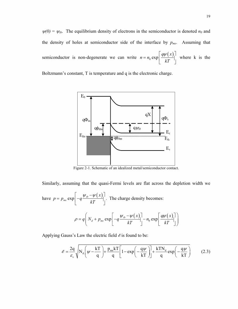
18
that in the metal Φm then electrons will be transferred from the metal into the
semiconductor, resulting in the formation of an abrupt discontinuity or barrier at the
interface. Ideally, the intrinsic n-barrier height φibn can be determined by:
( )ibn mq q Xφ = Φ − (2.1)
where Φm is the work function of the metal and X is the difference between the vacuum
level and conduction band edge or electron affinity, see Figure 2-1. The charge in the
metal can be modeled as a delta function because the Fermi level is in the conduction
band and there are many carriers. In the semiconductor, however, the Fermi level is in
the energy gap and fewer carriers are available to balance the charge induced on the
surface by the metal. As a result, charge is depleted from the metal/semiconductor
interface into the bulk of the semiconductor, shown schematically in Figure 2-1. The
intrinsic band bending ψib in the semiconductor is given by
ib m sψ = Φ − Φ (2.2)
The region of band bending, in which the charge is modified from that in the bulk, is
called synonymously the depletion or the space-charge region.
This intuition can be made more rigorous using Gauss’s law. The charge density
ρ is given by the charge neutrality condition:
( )dq N p nρ = + −
where Nd is the bulk doping concentration of donors (n-type wafer), p is the
concentration of holes and n is the concentration of electrons. Following the analysis of
Rhoderick (1988) we denote the electrostatic potential at a distance x from the interface
by ψ(x). We assume that ψ(x) is zero at infinity and from the discussion above we have
19
ψ(0) = ψib. The equilibrium density of electrons in the semiconductor is denoted n0 and
the density of holes at semiconductor side of the interface by pms. Assuming that
semiconductor is non-degenerate we can write ( )0 exp
q xn n
kTψ
=
where k is the
Boltzmann’s constant, T is temperature and q is the electronic charge.
E0
Efm Efs
qΦm
qφibn qψib
Ev
Ec
qΦs qX
qφibp
Figure 2-1. Schematic of an idealized metal/semiconductor contact.
Similarly, assuming that the quasi-Fermi levels are flat across the depletion width we
have ( )exp ibms
xp p q
kTψ ψ−
= −
. The charge density becomes:
( ) ( )0exp expib
d ms
x q xq N p q n
kT kTψ ψ ψ
ρ −
= + − −
Applying Gauss’s Law the electric field E is found to be:
ms dd
s
p kT kTN2q kT q qN 1 exp expq q kT q kT
ψ ψψε
= − + − − + − E (2.3)
20
where εs is the dielectric constant of silicon. In general such a complicated form of the
electric field is not necessary. Assuming that ps is negligible and qψ >> kT, the
expression is simplified to the standard depletion approximation:
d
s
2qN ψε
=E . (2.4)
This is equivalent to assuming that the charge is constant in the depletion width W:
ρ ≅ qNd for x < W and 0 elsewhere. The depletion width is defined as:
2 sib
d
kTWqN q
ε ψ
= −
(2.5)
Under applied bias the potential and depletion widths are modified. Exactly
where the bias is dropped depends on which transport process dominates, as discussed in
the next section. However, if all of the bias is dropped somewhere between the Fermi-
level in the metal and the quasi-Fermi level in the semiconductor, the above equations
can be easily altered to account for this. Applying a positive (negative) bias to the metal
increases the number of carriers at the semiconductor surface, therefore decreasing
(increasing) the electrostatic potential and the band bending. We see that the under an
applied bias V, the electrostatic potential ψ and band bending ψιb in equations (2.3), (2.4)
and (2.5) are replaced respectively by ψ - V and ψιb - V.
Experimentally it is found that equations (2.1) and (2.2) do not correctly predict
the barrier height and band bending. It is believed that interface states are responsible for
altering the barrier, an explanation first suggested by Bardeen in 1947. Surface states
exist at the interface, adding an extra charge and thus altering the potential. They are
characterized by a neutral level φ0 , such that if the Fermi level is above the neutral level,
21
the surface contains a net positive charge and the barrier height is effectively reduced.
This leads to ‘Fermi level pinning’ in which the barrier is pinned by a high density of
such states.
The Bardeen model was proposed by considering an interfacial oxide in-between
the metal/semiconductor surface and has been reconsidered so as to explain interface
states without this layer. There are primarily two ideas as to the origin of these states:
metal induced gap states (MIGS) and defects at the interfaces. In the first case, interface
states arise from the tails of the metal electron wavefunctions extending through the
interface. In the latter model, the termination of the bulk periodic potential of both
materials leads to defect states extending across the metal/semiconductor interface.
These models are discussed in detail in Rhoderick (1988). Although there has been some
success in explaining the experimental data, certain issues remain troubling because some
of the major assumptions have been shown to be without basis. More recently, it has
been suggested that chemical bonding is the primary mechanism in the formation of the
Schottky barrier height and can lead to an apparent Fermi level pinning effect (Tung
2000).
Despite the uncertainty as to the precise physics that describes the Schottky
Barrier formation, the barrier heights at metal/semiconductor interfaces can be
determined from experimental methods and are well represented in the literature. It will
be convenient to distinguish the p- and n- barrier heights. We denote φibn as the n
intrinsic barrier, the abrupt discontinuity between the Fermi level in the metal and the
edge of the conduction band and φibp as the p intrinsic barrier, the abrupt discontinuity
between the Fermi level in the metal and the valence band edge in the semiconductor.
22
The sum of the two barrier heights equals the gap of the semiconductor, (Eg = φibn + φibp).
In general, we assume the barrier height and determine the banding bending ψιb :
ib in c fq q (E E )ψ φ= − − . (2.6)
At g dc f
i
E NT 100K, E E kT exp2 n
> − = −
, where ni is the intrinsic carrier concentration.
Below this temperature, one must consider the effects of freeze-out. At 4K
c f dE E E− ≈ where Ed is the energy of the donor level.
The Schottky Barrier MOSFETs considered in this thesis use PtSi as the metal.
Silicide formation occurs when a metal is deposited on silicon and subsequently
annealed. (For an excellent discussion of silicide formation, see Murarka 1983.)
Silicide/silicon contacts are superior to metal/silicon contacts because the interface is
formed below the surface of the silicon. The contacts are therefore not subject to defects
from the silicon surface, but to the intrinsic properties of the metal/semiconductor
interface. We therefore expect the barrier height to be pinned either by the MIGS model
mentioned above or by the more recent chemical bonding model. From the SBMOSFET
point of view, silicides are the best candidate for the source and drain because the metal
remains unreacted on any surrounding oxide and can be selectively etched away with
respect to the silicide. In the following chapter, we find the p-type barrier under
inversion to be ~0.2 eV, which agrees well with previously reported PtSi/Si Schottky
barriers (Andrews 1970a; McCafferty 1996).

23
2.2. Transport Mechanisms in Metal/Semiconductor Contacts
At room temperature ideal Schottky barriers exhibit rectifying behavior due to emission
over the top of the barrier into the metal. This transport can be dominated either by
thermionic emission or by the drift/diffusion process in the depletion region. These two
transport mechanisms can be understood by considering the position of the quasi-Fermi
level, depicted in Figure 2-2. If the transport occurs at the barrier, as is the case for
thermionic emission, the bias will be dropped at the interface and the limiting resistance
is due to electrons having enough thermal energy to surmount the barrier. If, on the other
hand the drift/diffusion limits the transport, the bias will be dropped over the depletion
region and the dominant resistance is due to the electrons traveling through the depletion
region. The larger the Schottky barrier and the band bending, the more likely thermionic
emission will dominate. The I-V characteristics of both mechanisms are very similar;
however in the reverse bias the drift/diffusion current density does not saturate but
increases as ~|ψb - V|1/2.
qψib-V
Ev
Efs
qφibn
qV
Ec
Diffusion
Thermionic Emssion
Figure 2-2. Comparison of the quasi Fermi level in diffusion and thermionic emission theories. Note that the quasi-Fermi level for thermionic emission and tunneling will be identical.

24
At low temperatures, the dominant transport through a Schottky Barrier is
tunneling: either direct tunneling (field emission) at the quasi-Fermi level or thermal
assisted tunneling (thermionic field emission). While direct tunneling occurs at the
quasi-Fermi level, thermal assisted tunneling occurs above the Fermi level but below the
top of the barrier. The tunneling current may also exhibit rectifying behavior; however,
the polarity of the rectification is opposite that observed in thermionic/diffusion current.
In thermionic emission, the large positive current is a result of the lowering of the band
bending in the semiconductor and thus easier transport of carriers from the semiconductor
into the metal, depicted in Figure 2-3. The transport in the tunneling regime is more
complicated and depends on the magnitude of the bias. For very small bias the current
transport in both directions should be linear. When the bias is smaller than the barrier
height, however, tunneling in the reverse biased contact may be larger, because the
tunneling distance is smaller than in the forward biased contact, as depicted schematically
in Figure 2-5. Tunneling can dominate the reverse bias transport of leaky Schottky
barriers and can be significantly greater than the reverse saturation current of thermionic
emission or the V1/2 dependence of drift/diffusion. An understanding of these processes
is fundamental in the research in this thesis. In particular, fabrication of high-quality
SBMOSFETs at room temperature requires that the thermionic/diffusion current
dominate the transport in the sub-threshold regime. Direct and thermal assisted tunneling
become relevant in the ‘on’ state of the device and also at low temperatures.

25
Ef
qφibn qψib
Ev
Ecqφibp
Efs
q(ψib-V)
Ev
Ec
q(ψib-V)
Ev
Efs
qφibn
qφibn
qV
qV
Ec
Figure 2-3. Schematic of the band bending indicating thermionic emission transport. a) The equilibrium band diagram. b) The band diagram with negative bias applied to the metal. Note that increasing the magnitude of the bias does not change the barrier qφibn of electrons from the metal and therefore the current is saturated. c) The forward bias band diagram where increasing the bias results in a decrease in the band bending qψib and thus an increase in current.
In addition, there are other transport mechanisms such as recombination in the
space-charge region and recombination in the neutral region. The first process takes
place via localized states and results in an ideality factor between one and two. The
second occurs, for instance, when the Schottky barrier on an n-type material is greater
than half the band gap and thus the semiconductor adjacent to the metal contains a high
density of holes, which can diffuse into the neutral region under forward bias. This is
effectively a p-n junction and the current density can be written from ordinary p-n
junction theory. Neither of these processes is relevant for this thesis research. The first
mechanism may show up in leaky SBMOSFETs, but the leaky SBMOSFETs that are
discussed in Chapter 4 have ideality factors greater than 2. The literature on PtSi
26
Schottky barriers indicates that majority carrier injection dominates the transport,
(Andrews 1970a), and thus the second mechanism is not important either.
2.2.A Transport Over the Barrier
In this section we review both thermionic emission and diffusion theory. We derive the
thermionic emission equation in 3D and extend the analysis to include a two-dimensional
density of states. Next the diffusion theory is introduced and a combined theory is briefly
discussed. Finally, we relate these theories to transport in SBMOSFETs, a topic that will
be discussed in much greater detail in Chapter 4.
Thermionic Emission
Thermionic emission assumes that the bias is dropped abruptly at the
metal/semiconductor interface and neglects scattering adjacent to the barrier. The
electron concentration on the semiconductor side (ss) of the boundary is thus given by:
[ ]ibnss c
q Vn N exp
kTφ −
= −
and similarly on the metal side (ms): ibnms c
qn N expkTφ = −
,
where Nc is the effective density of states in the conduction band. Electrons are assumed
to have a Maxwellian distribution of velocities and from kinetic theory we obtain:
( )1/ 2
rkTv 2 m*π= (see Kittel 1980, p. 393) where m* is the effective mass in the
semiconductor. The current density is the sum of the currents from the semiconductor to
the metal ( sm ss rJ qn v= ) and the metal to the semiconductor ( ms ms rJ qn v= ). Putting this
together we find:

27
1/ 2
exp xp 12 *
ibnsm ms c
qkT qVJ J J N em kT kT
φπ
= − = − − (2.7)
Note that ( )3/ 2
2c2 m*kTN 2 hπ= is the effective density of states in the conduction
band⊥. Putting this in equation (2.7) we obtain the well-known thermionic emission
equation:
* 2 exp exp 1ibn dss
q qVI AA TkT kTφ = − −
(2.8)
where 2
6 2 23
4 m*qkA* 1.2x10 m* m Am Kh
π − −= = is the Richardson constant and m* is the
effective mass and A is the cross sectional area into which carriers are injected. For
electrons in Si, the constant energy surfaces are anisotropic and m* must by summed over
the six valleys: m* = 2mt + 4(mlmt)1/2 = 2.05 in the <100> direction. For holes in Si, the
two energy maxima at k = 0 give rise to an approximately isotropic current flow from
both the light and heavy holes: m* = (mlh + mhh ) = 0.65 and thus A* = 780,000 Am-2K-2 =
78 Acm-2K-2 for holes in silicon. We note that the Richardson constant does not include
the effects of optical phonon scattering and quantum mechanical reflection. This has
been included for instance in Crowell (1966), and experimentally verified by Andrews
(1970b). The effective Richardson constant which accounts for this is found to be A** =
32 Acm-2K-2 for holes in silicon.
In SBMOSFETs, conduction is restricted to the 2DEG underneath the gate and
thus the expressions for the effective density of states and Maxwell distribution of
⊥ The effective density of states in the conduction band is the 3D partition function of an atom of mass m* confined to a cubical box of volume L3. A derivation can be found, for instance, in Kittel (1980) pg 73.

28
velocities can be rederived assuming the restricted dimensionality:
( )2c2 m*kTN 2 hπ= and 2r 3
1 kTv2 2m
π= . The 2D thermionic emission equation is thus:
| 3/ 2 exp exp 1ibn dss
q qVI wATkT kTφ = − −
(2.9)
where ( )3/ 2| 1 3/ 2
2
q 2m* kA 0.114 Am K
hπ − −= = is the Richardson constant in two
dimensions and w is the width in which carriers are injected and the numerical value was
calculated for holes in silicon.
As mentioned earlier, the MSM structure consists of two back to back Schottky
barriers: one forward biased and one reverse biased. If the barriers are not transparent to
current flow and if there are no leakage paths in the contacts, transport through the
reverse bias barrier should limit the current flow. Recall that a reverse bias barrier
implies that current flows from the metal into the semiconductor.
Diffusion Theory
In diffusion theory the bias is assumed to drop inside the depletion region and the barrier
does not present an obstacle to the transport (see Figure 2-2). The derivation of the
formula can be found in numerous references (Sze 1981; Rhoderick 1988) and in the
interest of brevity we state the result for the current density:
ibn dsc max
q qVI AqN exp exp 1kT kTφµ = − −
E (2.10)
where µ is the mobility in the bulk semiconductor and Emax is the maximum electric field.
The diffusion theory results in an equation that is very similar in form to the thermionic
29
emission theory, equation (2.8). The main difference is that the Emax, given by either
equation (2.3) or equation (2.4), is dependent on bias voltage. In the depletion
approximation we have that max b Vψ∝ −E . Note that the temperature dependence of
the diffusion and thermionic emission theories are very similar. Equation (2.10) is for a
3D geometry but can be simply modified in the 2D case by using the 2D expression for
Nc that was noted earlier.
We can combine the thermionic emission and diffusion theories by considering
the two mechanisms to be in series and finding the position of the quasi-Fermi level that
equalizes the current flow through each of them. Following Crowell (1966) this can be
written in the form:
c r ibn
r
d
AqN v q qVI exp exp 1v kT kT1 v
φ = − − +
(2.11)
where vr is the thermal velocity introduced when deriving the thermionic emission
equation and vd is the velocity due to drift and diffusion of electrons at the top of the
barrier. At its maximum value, vd = µEmax. The smaller of the two velocities will
dominate the transport
In order to distinguish the two processes, we note that the drift velocity is related
to the mean free path. If the mean free path is small, the drift velocity is small and thus
few carriers make it to the barrier. If the mean free path is large, most of the electrons
arriving at the depletion layer reach the metal and the transport is limited by thermionic
emission. Finally, we note that a more rigorous treatment of transport over the barrier
has recently been developed, which is accurately able to account for scattering a distance
of kT/q from the interface (Lundstrom 1996).

30
2.2.B Field and Thermionic Field Emission
Where thermionic emission is a ‘classical’ effect, tunneling or field emission of carriers is
purely quantum mechanical. Thermionic (or thermal-assisted) field emission dominates
the transport when carriers have enough thermal energy to tunnel through a portion of the
barrier near the top, but not enough energy to reach the top and be emitted over it. Such
transport occurs at high temperatures and electric fields. At low temperatures, the
thermal energy of the carriers is negligible and the transport is dominated by direct
tunneling, which occurs when carriers with Fermi velocity vf are emitted from the metal
(semiconductor) into the semiconductor (metal). These processes are depicted in Figure
2-4.
Ec
Ev
qV
TF
F
Figure 2-4. Band diagram indicating the different energies associated with thermionic field emission (TF) and Field emission (F).
Direct tunneling in Schottky barriers was in fact the first theory of rectification for
metal-semiconductor contacts (Wilson 1932); however, it did not accurately describe the
transport because the rectification gave the wrong sign (Davidov 1938). It was
subsequently replaced by the thermionic emission and diffusion theories mentioned in the
previous section. Thermal assisted and direct tunneling in metal/semiconductor contacts
were considered in papers by Padovani (1966), Rideout (1970) and Chang (1970) in order
to explain deviations from the ideal behavior predicted by thermionic emission/diffusion

31
theories. While the theories of Padovani (1966) and Rideout (1970) are based on the
WKB approximation for a parabolic barrier and result in closed form solutions, Chang
(1970) obtains the transmission coefficients by a Taylor expansion method using a
Thomas-Fermi potential scheme and involves a numerical integration. This method is
more general in that it takes into account image-force lowering, quantum-mechanical
reflection and uses Fermi-Dirac statistics so that it is applicable to degenerate
semiconductors. However, we are most interested in the direct tunneling current when
the applied voltage is much smaller than φibn, and in this case the WKB method of
Rideout (1970) and Padovani (1966) has been shown to yield similar results to that of
Chang (1970).
For comparison with experimental results, the simplest and most comprehensive
treatment is the paper by Padovani (1966) with the appropriate corrections from Padovani
(1971). In this paper different expressions for the I-V are given in four regimes: forward
bias at low temperatures, forward bias at intermediate temperatures, reverse bias at low
temperatures, and reverse bias at intermediate temperatures. The expressions are quite
complicated but reasonable forms can be obtained in the different limits, and a brief
summary is thus given in Appendix B.
To obtain some intuition as to how the current changes with applied bias, we
model the band diagrams under zero and ±50 mV in a degenerate semiconductor (Figure
2-5). In this example, the n-type barrier is 0.2 eV and the doping is 4 X 1018 cm-3.
Without bias, the depletion width is 8.12 nm. When a (negative) positive bias of (-) 0.05
V is applied to the metal, the depletion width is (increased) reduced to (9.08 nm) 7.0 nm.

32
More importantly, however, the tunneling distance in the positive direction is larger than
that in the negative direction.
Figure 2-5. Schematic of the band diagram when tunneling occurs. The conduction band is shown at zero bias (solid line) and ±50 mV (dashed and dotted lines). The black lines with arrows at either end indicate the tunneling distance in the forward xft and reverse xft bias directions. Note that depletion widths are parabolic, not triangular as is assumed for the Fowler-Nordheim transmission coefficient in (2.12).
To obtain an analytic expression, we assume that the barrier is triangular and that
Vds << φibn. Using the WKB approximation the transmission probability P is:
( )3/ 24 2 *exp
3ibnm q
Pφ
= − E
(2.12)
where E is the electric field (see for instance, Landau 1994, p. 180). For a
metal/semiconductor contact E is approximately given by equation (2.4). We assume that
the semiconductor is degenerate so that Ef = Ec, and the band bending is equal to the
barrier height at zero applied bias. In the forward bias direction, the height of the tunnel

33
barrier is reduced, and thus, φibn in equations (2.12) and (2.4) is replaced by (φb – V). The
transmission probability becomes:
( )00
4exp
3ibn V
PE
φ − = −
(2.13)
where 00 2 *s
NEmε
= . In the reverse bias direction, only the φb in the depletion width is
replaced by (φibn – V) because only the slope of the electric field is modified, not the
height from which tunneling occurs. This results in a transmission probability of:
( ) ( )1 1
2 2
00
4exp
3b ibn V
PE
φ φ − = −
(2.14)
The current for electrons tunneling from a metal to a semiconductor can be
written as:
( ) ( ) 3 0 0
4 * E
ms m f s f xmJ q dE f E E f E qV E PdE
hπ ∞
= − − + −∫ ∫ (2.15)
where ( ) ( ) and s f m ff E E f E qV E− + − are the Fermi Dirac functions in the semi-
conductor and metal. We note that the integral over Ex is constant and integration by
parts can be used for the other integral. Setting Ef = 0 for simplicity, we find:
00 00300 00 00
48 * 3 3exp exp 1 exp3 4 4
ibnm V VJ q E E Vh E E E
φπ = − − +
(2.16)
The assumption of a triangular barrier works reasonably well in the forward bias
case; however, in the reverse bias direction it dramatically over-estimates the tunneling
distance and thus underestimates the current. For small bias, however, the reverse and

34
forward directions should be approximately equal and thus equation (2.16) can be used.
It can be simplified when V << φibn:
00200
4*6 exp3
ibnAJ VEk E
φ = −
(2.17)
where A* is Richardson’s constant.
2.3. The MOS Capacitor
Silicon is technologically the most important semiconductor because of its ability to
produce compatible semiconductor and insulator materials. MOS technology blossomed
in the 1970s after the discovery of the integrated circuit in 1959, the invention of CMOS
in the 1960s and the ever-improving fabrication technologies. In this section we review
the basic MOS capacitor and later use it in simulating the sub-threshold behavior of
SBMOSFETs. In Section 2.4, the device physics of MOSFETs is discussed and serves as
a basis of comparison for SBMOSFETs.
The physics of Metal/Oxide/Semiconductor (MOS) systems is very similar to the
metal/semiconductor contact and the relative energy levels of the MOS system when
separated are shown schematically in Figure 2-6. Like the metal/semiconductor contact,
charges induced from the metal result in band bending into the bulk semiconductor. The
difference lies in that the MOS system functions as a capacitor and thus there is no
current flow. In particular, the oxide is incapable of transferring charge because it
(ideally) has no mobile charge and it therefore sustains a voltage drop.
35
qΦm
EfEc
Ec
qχ
Ev
Ev
M O S
EfEi
E0
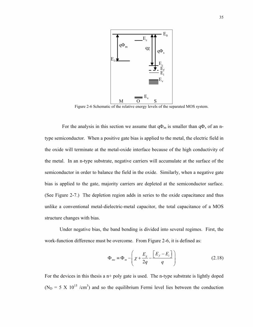
qΦs
Figure 2-6 Schematic of the relative energy levels of the separated MOS system.
For the analysis in this section we assume that qΦm is smaller than qΦs of an n-
type semiconductor. When a positive gate bias is applied to the metal, the electric field in
the oxide will terminate at the metal-oxide interface because of the high conductivity of
the metal. In an n-type substrate, negative carriers will accumulate at the surface of the
semiconductor in order to balance the field in the oxide. Similarly, when a negative gate
bias is applied to the gate, majority carriers are depleted at the semiconductor surface.
(See Figure 2-7.) The depletion region adds in series to the oxide capacitance and thus
unlike a conventional metal-dielectric-metal capacitor, the total capacitance of a MOS
structure changes with bias.
Under negative bias, the band bending is divided into several regimes. First, the
work-function difference must be overcome. From Figure 2-6, it is defined as:
2f ig
ms m
E EEq q
χ − Φ ≡ Φ − + −
(2.18)
For the devices in this thesis a n+ poly gate is used. The n-type substrate is lightly doped
(ND = 5 X 10¹⁵ /cm3) and so the equilibrium Fermi level lies between the conduction
36
band edge and the intrinsic Fermi level. At the surface of the MOS capacitor we see that
ln 0.23 2
g Dms
i
E kT Nq eVq n
Φ = − = −
. For a small negative bias, this potential is reduced
until the potential at the surface is equal to the potential in the bulk, known as the flat
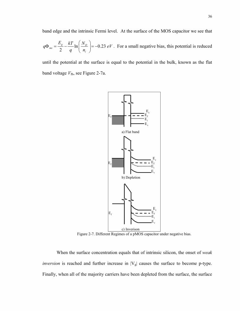
band voltage Vfb, see Figure 2-7a.
Ef
Ec
Ev
EfEi
Ef
Ec
Ev
EfEi
Ef
Ec
Ev
EfEi
a) Flat band
b) Depletion
c) Inverison Figure 2-7. Different Regimes of a pMOS capacitor under negative bias.
When the surface concentration equals that of intrinsic silicon, the onset of weak
inversion is reached and further increase in |Vg| causes the surface to become p-type.
Finally, when all of the majority carriers have been depleted from the surface, the surface

37
potential is as p-type as the bulk is n-type, known as strong inversion. At this point, the
depletion region has reached its maximum and subsequent negative gate bias, induces
minority carriers to the surface from recombination centers (See Figure 2-7c).
These regions can be quantified in terms of the gate voltage, Vg. An applied bias
at the gate is dropped partially across the oxide (ψox) and partially across the silicon (ψs):
g ms ox sV ψ ψ= Φ + + , where Φms is the metal semiconductor work function difference
discussed above. The potential in the semiconductor varies as a function of depth (ψ(z))
so that at the surface ψ(z = 0) = ψs, which represents the band bending from the bulk
silicon to the surface underneath the MOS capacitor. The potential across the oxide can
be written as 0)s s sox
ox ox
Q zC C
εψ == =
E ( where Qs is the charge at the surface, εs is the
dielectric constant in the semiconductor and Es(z = 0) is the electric field at the surface.
Using the depletion approximation, Es(z = 0) can be calculated exactly from Poisson’s
equation (Nicollian 1981). The result is:
( ) ( ) ( ) ( )( )1/ 2
122
exp 1 exp 2 exp 1D sg ms s s s b s s
ox
qNV
Cε
φ ψ ψ β ψ β ψ β ψ β ψ β = − ± − + − + − − − (2.19)
where qψb = Ef – Ei = kTln(ND /ni) is the potential in the bulk, and β = q/kT. This
approximation assumes that the free carrier distribution between the neutral bulk and the
depletion region is a step function. Surface quantization is also neglected and the
densities of states in the conduction and valence bands are assumed to be constant with
electric field. Furthermore, the impurity concentration is assumed to be uniform up to the
surface, and the solution is only valid for the non-degenerate case.

38
This equation may be solved by numerical iteration; however, we can now
determine the points at which accumulation, depletion and inversion occur. For ψs = 0,
Vg = Φms and the flatband condition is reached. Thus when Vg > Φms, accumulation
occurs and the surface potential is negative. For ψs << 0, the first term in square brackets
dominates. When Vg < Φms, the carriers are depleted from the surface of the
semiconductor and when ψb > ψs > 0, the second term in brackets ((ψs β)1/2 ) dominates.
Inversion occurs when ψs > ψb and thus the surface becomes more p-type than n-type.
The onset of strong inversion occurs when ψs = 2ψb and at this point the surface is as p-
type as the bulk is n-type, called as the threshold voltage, Vt. Beyond strong inversion,
the surface potential does not increase as rapidly as previously. At this point ψs >> ψb
the fourth term dominates ( ( )exp sψ β ). (An excellent discussion can be found in Wolf
1995.)
It is convenient to define the surface concentration of holes and electrons:
( )exp 2s D s bp N β ψ ψ= −
( )2
exp 2is s b
D
nnN
β ψ ψ= − −
Since no current flows in an MOS capacitor, the carrier concentration must be in
equilibrium: 2s s in p n= . Note that at the onset of weak inversion ( s bψ ψ= ), s s in p n= = .
We now calculate the gate bias at the onset of these regimes. Table 1 shows
some of the important numbers relevant to the device and Table 2 shows the onset of the
important regimes. To perform these calculations for temperatures other than 300 K one
needs to determine the change in both the intrinsic carrier concentrations and the number
39
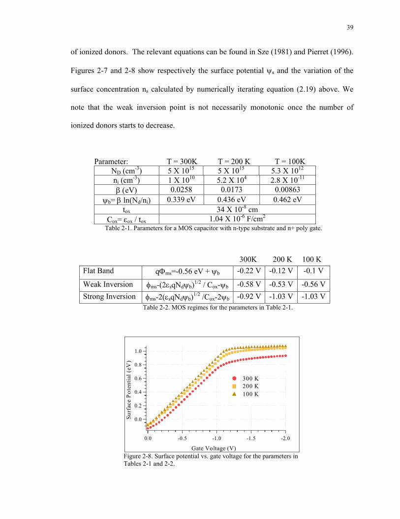
of ionized donors. The relevant equations can be found in Sze (1981) and Pierret (1996).
Figures 2-7 and 2-8 show respectively the surface potential ψs and the variation of the
surface concentration ns calculated by numerically iterating equation (2.19) above. We
note that the weak inversion point is not necessarily monotonic once the number of
ionized donors starts to decrease.
Parameter: T = 300K T = 200 K T = 100K ND (cm-3) 5 X 10¹⁵ 5 X 10¹⁵ 5.3 X 10¹² ni (cm-3) 1 X 10¹⁰ 5.2 X 10⁴ 2.8 X 10⁻¹¹
β (eV) 0.0258 0.0173 0.00863 ψb= β ln(Nd/ni) 0.339 eV 0.436 eV 0.462 eV
tox 34 X 10-8 cm Cox= εox / tox 1.04 X 10⁻⁶ F/cm2
Table 2-1. Parameters for a MOS capacitor with n-type substrate and n+ poly gate.
300K 200 K 100 K Flat Band qΦms=-0.56 eV + ψb -0.22 V -0.12 V -0.1 V
Weak Inversion φms-(2εsqNdψb)1/2 / Cox-ψb -0.58 V -0.53 V -0.56 V Strong Inversion φms-2(εsqNdψb)1/2 /Cox-2ψb -0.92 V -1.03 V -1.03 V
Table 2-2. MOS regimes for the parameters in Table 2-1.
1.0
0.8
0.6
0.4
0.2
0.0Surf
ace
Pote
ntia
l (eV
)
-2.0-1.5-1.0-0.50.0
Gate Voltage (V)
300 K 200 K 100 K
Figure 2-8. Surface potential vs. gate voltage for the parameters in Tables 2-1 and 2-2.

40
1020
1015
1010
105
100Surf
ace
Con
cent
ratio
n(cm
-3)
-2.0-1.5-1.0-0.50.0Gate Voltage (V)
300 K 200 K 100 K
Figure 2-9. Hole surface concentrations vs. gate voltage for the parameters listed in Tables 2-1, and 2-2.
While this approximation works reasonably well at higher temperatures, at lower
temperatures the Fermi-Dirac function should be used and a closed form expression
cannot be obtained. Using Silvaco simulation software, we calculate the carrier
concentration of a MOS capacitor in order to obtain a more accurate result. It is found
that method above over-estimates the number of carriers in strong inversion.
Furthermore, according to Silvaco, as the temperature is decreased, the number of
carriers in the strong inversion regime slightly decreases whereas in Figure 2-9 it
increases. The surface concentration is used throughout the thesis to obtain estimates of
the current and for T > 150 K, the carrier concentrations from Silvaco are used. A further
discussion is found in Section 4.2.

41
2.4. The Conventional MOSFET
We now briefly outline the device physics of the conventional MOSFET as a basis of
comparison for the SBMOSFET in later chapters. Figure 2-10 depicts a schematic of a
conventional pMOSFET, which consists of two back-to-back p-n junctions topped by an
MOS capacitor. Before strong inversion (|Vg| < |Vt|), the device is in the ‘off’ state and
any current that flows is called the sub-threshold current. When gate is biased beyond
strong inversion, |Vg| > |Vt|, a conducting channel is formed between the two junctions
and the transistor is in the ‘on’ state. The |Vg| value at which inversion occurs at the drain
of a pMOSFET is greater than that in a MOS capacitor with the same parameters because
the applied drain bias raises the p-quasi-Fermi level. In addition the depletion layer
width into the bulk silicon is a function of the Vds bias and at the onset of strong inversion
the surface potential at the drain is given by: 2s DS BVψ ψ+ (Sze 1981). A detailed
calculation of the space charge is similar to that obtained for the MOS capacitor.
p+ p+
n+ poly gate
Sidewall oxideMetal
Oxide
Figure 2-10. Schematic of a conventional MOSFET.
Device Transport Equations
In order to obtain the transport equation for basic MOSFET characteristics we assume: 1)
an ideal MOS capacitor, 2) current transport is dominated by the drift of carriers, 3)
constant mobility in the inversion layer, 4) uniform channel doping, 5) the transverse

42
field is much smaller than the longitudinal field (also known as the gradual channel
approximation). As shown in many textbooks (Muller 1986; Wolf 1995; Sze 1981) in the
on state this yields:
( ) 2D n ox G t ds ds
WI C V V V VL
µ= − − (2.20)
at |Vds| < (|Vg| – |Vt|). Saturation occurs when |Vds| > (|Vg| – |Vt|) and results in a current
of:
( )2D n ox G T
WI C V VL
µ − (2.21)
These equations predict zero current when |Vg| < |Vt|. In the off state, however,
diffusion is the dominant transport mechanism in the channel. The sub-threshold current
can be shown to be (Sze 1981, p. 446):
( )( )
2 2
22 1 exp expi s ox ox ds ssub s
D ox D
Wn t q C qV qILN L kT kTkT
ε ψµ βψε
− = − (2.22)
Isub is thus independent of Vds for Vds > 3kT/q. Ideally, the sub-threshold current is very
small and then increases rapidly at turn on. One measure of this is the sub-threshold
swing defined as:
( ) ( ) ( )ln 10 ln 10 1ln
g D
d ox
dV kT CSd I q C
≡ ≅ +
(2.23)
The minimum and thus ideal sub-threshold swing occurs when the thickness of the oxide
goes to zero because then CD/Cox = 0. At room temperature the ideal sub-threshold swing
is thus 60 meV/decade. As the temperature is decreased the sub-threshold swing
becomes sharper, as was shown in Figure 2-8. We shall see in the later chapters that an
SBMOSFET does not necessarily follow this behavior as temperature is decreased

43
because of the different transport mechanisms that occur as the carrier concentration and
temperature are changed.
In this simple analysis, we have assumed that the drift velocity varies linearly
with electric field and thus that the mobility is constant. In fact at high electric fields,
velocity saturation occurs, caused by hot electrons transferring their energy to the lattice.
This is observed by two changes from the ideal Id vs Vd characteristics: the saturation
current is reduced and is linearly dependent on gate voltage.
Device Scaling
The goal of MOSFET scaling is to obtain faster devices with higher drive currents, while
still maintaining the device characteristics described above. There are various sets of
scaling rules that can be applied to MOS design parameters when reducing the
dimensions of an established MOS process. (An excellent discussion is found, for
instance, in Sze 1998). Such rules can approach fundamental limits such as the gate
oxide cannot be made much smaller than ~15 Å because of substantial gate leakage into
the channel. In this section we briefly discuss where degradations in device performance
occur and to what extent these changes are acceptable. Device characteristics that are
affected include the threshold voltage, the sub-threshold slope, and the ‘off’ state current.
When the MOSFET is made smaller the gradual channel approximation no longer
holds because the depletion widths of the source and drain make up an important part of
the channel length. As a result, the charge in the channel is greater than the MOS theory
predicts and the threshold voltage is decreased. This effect is known as surface Drain-
Induced-Barrier-Lowering (DIBL) and can be quantified by measuring the Id vs. Vg

44
characteristic and determining the change in Vg for different Vds values at a fixed value of
Id (typically 1 µAmp / µm). An acceptable DIBL is < 100 mV/V. DIBL should be
measured for Vds > 3kT/q so that the normal deviation in sub-threshold slope is not
mistaken for device degradation.
When the depletion width at the source and the depletion width at the drain
become so large that they interact, the barrier for carrier transport is reduced. This effect
is known as punch-through and it has several consequences. First, in the ‘off state’ when
the depletion widths are the largest, it causes an increase in the off state current. In the
‘on state’, the effect worsens as Vds is increased and results in ‘non saturating’ Id vs Vd
characteristics. A typical acceptable sub-threshold leakage current is ~ 1 nA/ µm.
Punch-through is typically quantified by observing the sub-threshold swing St for
different channel length devices. The maximum acceptable sub-threshold swing is ~100
mV/decade
2.5. MOSFETs At Cryogenic Temperatures
Low temperature properties of MOSFETs were studied in great detail during the 1970’s.
This work is particularly well summarized in a review by Ando (1982). The interest in
the low temperature properties of Si MOSFETs began because of the quantum effects
exhibited by the two-dimensional electron gas (2DEG). In a magnetic field the constant
density of states is split into quantized Landau levels and provided evidence for their
2DEG nature.
Transport measurements have also focused on localization, which is especially
interesting in inversion layers because the electron concentration can be easily varied.
45
Localization is the process by which the conductivity of a conductor is modified due to
the spatial localization of electronic states. In the strong localization regime, which was
introduced in 1958 by Anderson, the localization effect causes a three dimensional
conductor to become insulating, also known as a Metal Insulator Transition (MIT). The
scaling theory of localization was introduced in 1972 by Edwards and Thouless and
reformulated in 1979 by Abrahams. This theory generalized localization to conductors of
different dimensions. It also included the weak localization regime in which the
conductance of a metal with dimensions smaller than the phase coherent length is
reduced because of interference between different scattering sites. This phenomenon can
be destroyed by a small magnetic field and thus provides a method of determining the
phase coherence length of a conductor (Datta 1995).
Localization is still an active area of research today. In particular, one of the
important issues is which transport mechanism dominates in which temperature regime of
samples of different sizes. Traditionally, transport falls into two categories: activation to
a neighboring localized state and variable range hopping (Imry 1999). In MOSFETs,
resonant tunneling between localized impurity states is also observed at low enough
temperatures (Fowler 1988). Scaling theory predicts that a MIT cannot occur in a 2DEG;
however, in 1994, Kravchenko reported observation of such a transition in a very clean
(high mobility) MOSFET. One model that may explain this result is that a very clean
2DEG consists of a random network of quantum point contacts in which the conductance
through each point contact is quantized (Meir 1999).
Closely related to weak localization is the phenomenon of universal conductance
fluctuations (UCF). When the dimensions of a conductor are made very small, the

46
conductance is no longer a statistical average but depends on the transport through
localized states. While the average conductance is predicted by localization theory, large
variations can be observed. These variations are called UCFs. The transport process of
UCFs is due to activated hopping (the typical signature of weak localization) at higher
temperatures or resonant tunneling through discrete localized states as the temperature
goes to zero (Fowler 1982 and 1986, see Fowler 1988 for a review.). The significance of
this work is that it was one of the first observations of resonant tunneling in MOSFETs.
Another phenomenon that has been studied in MOSFETs is Coulomb Blockade.
It was first observed in narrow width double gate MOSFETs in 1989 (Scott-Thomas
1989). Coulomb Blockade is evidenced by periodic oscillations found in the conductance
vs gate voltage characteristics and a Coulomb staircase in the Id vs Vd characteristics. In
the case of a narrow channel MOSFET, the random charges found in the channel create
potential barriers along the length of the transistor. Each oscillation corresponds to the
addition of one electron onto this distribution of charges. More recently, Coulomb
Blockade in quantum dots formed by an impurity potential has been examined in quasi-
one-dimensional wires (Zhang 1998; Ishikuro 1996). Because quantum dots formed
with impurities contain fewer electrons, silicon based quantum dots formed in this way
can operate even at room temperature. Coulomb oscillations have also be observed in
very short but wide MOSFETs (L = 0.05 µm, w >> L), in which the blockade is also
caused by localized states (Sanquer 2000). Although this is not related to resonant
tunneling, we note that the droplet of electrons that exists in the narrow width can be
viewed as an artificial atom. We point out that neither localization, UCFs or Coulomb
Blockade caused by impurities in the channel were studied in this research on

47
SBMOSFETs. The main reason for this is that the transport in the SBMOSFET is
dominated by transport through the barrier and not that of the 2DEG.
2.6. Resonant Tunneling Through Impurities
In Chapters 6 and 7, we investigate the low temperature properties of the SBMOSFET.
While the majority of the transport can be dominated by the direct tunneling through the
Schottky barriers; transport can also take place through localized states. We find that the
states are caused by single impurities that exist in the vicinity of the barrier. In Chapter 6
we develop in greater detail the potential of the localized state and the effect it has on the
barrier. In this section, we present the background for that discussion. In particular, the
transport in quasi-1D channels via the Landauer-Buttiker formula is briefly discussed and
previous experimental and theoretical research on tunneling through localized states is
reviewed.
2.6.A. Landauer Formalism and Resonant Tunneling
Whereas the previous sections of this chapter focused on transport in three dimensions, a
discussion of tunneling through localized states requires a comprehension of transport in
quasi-one dimension. Two equivalent formalisms have been developed: Scattering (S) -
matrices (or Landauer-Buttiker formalism) and Green’s functions. The S-matrix
formalism considers a scattering matrix that relates outgoing waves amplitudes to
incoming wave amplitudes of different leads. From this, a transmission function can be
computed which is proportional to current, as we show below. The scattering matrix is

48
often divided into several sections, where each section is coherent. The Green’s
function approach is a ‘generalized’ S-matrix that allows the response due to an
excitation to be determined at any point, not just at the leads. In general, the Green’s
functions method is powerful when including effects of various interactions (electron-
electron, for instance). In this research we are not concerned with interactions and thus
the Landauer approach is sufficient.
We consider a quasi-one-dimensional conductor connected to two large contacts.
By quasi-1D, we imply that there are M possible channels or modes from the left contact
to the right contact. Furthermore, an electron does not suffer phase randomizing
collisions when traveling between the two contacts, e.g. transport is ballistic. Finally, the
probability that an electron from the left contact will arrive at the right contact is given by
the transmission probability T. If the difference in chemical potentials is small, the net
current between left and right contacts is:
fE
dn kI nqvMT q q MTdE m
µ = ∆ = ∆
(2.24)
where 2
1 *2
dn n k mdE k E kπ
∂ ∂= =
∂ ∂ is the density of states per unit energy per unit length of a
channel, M is the number of modes, assumed constant in energy. In general, we must
consider the effect of temperature. We assume for most of the thesis that the response is
linear and thus the current can be written as:
( ) ( ) ( )1 22
feI T E f E f E dE
h= − ∫ (2.25)
For small deviations from equilibrium, this becomes:

49
( ) 02f
feI T E dEh E
∂ = − ∂ ∫ (2.26)
From elementary quantum mechanics, a discrete state situated between two large
barriers gives rise to discrete energy levels. If the Fermi level is swept through the
energy level of the discrete state a resonant peak will be observed. In SBMOSFETs, this
is equivalent to sweeping the gate bias and measuring the drain current for a fixed Vds
value. In textbooks (Datta 1995), this is made more rigorous and it can be shown that the
transmission coefficient through such a resonance is well approximated by:
( ) ( )2 20
( )/ 2 / 2
L R
L R
T EE E
ηΓ Γ=
− + Γ + Γ
(2.27)
where the parameter X xdE Tdθ
Γ ≡ , Tx is the transmission coefficient through the left (L) or
right (R) barrier and θ is the phase shift acquired in one round trip through the barriers.
This is the well-known Breit-Wigner or Lorentzian approximation and an example is
shown in figure 2-11. We note that ΓL and ΓR represent the rate at which an electron
placed between the barriers will leak into the left and right leads. Finally, it is well
established that the peak value of the resonant tunneling current is not necessarily 2e2/h
and that any applied bias can dramatically reduce the value of the transmission
coefficient (Ricco 1994).

50
1.0
0.8
0.6
0.4
0.2
0.0
Lore
ntzi
an L
ineS
hape
-0.4 -0.2 0.0 0.2 0.4Energy
Figure 2-11 Example of the Lorentzian lineshape
2.6.B Previous Research on Localized States
Resonant tunneling through localized states has been well studied in previous research.
Most of the effort, however, has focused on incoherent transport. In this section we
review previous work on both coherent and incoherent transport but neglect systems
exhibiting electron-electron interactions such as the Kondo effect.
One of the first observations of resonant tunneling through discrete states was an
investigation of transport through Na ions in thin gate oxides of conventional MOSFETs
(Koch 1985). In these experiments, a thin gate oxide was used and NaCl was or was not
evaporated on the oxide before gate metal deposition. In the device with NaCl, the
differential conductance at the gate electrode showed peaks as a function of gate voltage.
The peaks were observed to shift with Vsd and the temperature dependence was obtained.
This experiment is similar to the SBMOSFET work in that the current is tunneling from a
3D contact into a 0D state and then into a 2DEG, and because the localized states exist in

51
a barrier. The researchers were not able to find a simple temperature dependence, nor was
Lorentzian fit obtained.
Another resonant tunneling experiment involved tunneling through impurities
located between two 2DEGs in a split gate MOSFET and was able to exhibit the
Lorentzian lineshapes. In particular, resonances associated with a localized state located
asymmetrically in the barrier were dramatically reduced with an applied magnetic field,
because of the unequal change in the leak rates of the left and right barriers (Kopley
1988). Further research showed that by contacting each of the 2DEGs separately, the
position of the impurity between the two barriers could effectively be modified (McEuen
1991).
A split gate technique in GaAs/AlGaAs structures has also been used to examine
Lorentzian lineshapes (McEuen 1990). This experiment was very similar to the split gate
technique in MOSFETs; however, the constriction was smaller and single electron
tunneling was in general observed instead of resonant tunneling. However, the presence
of an impurity in the constriction caused lineshapes, which could not be described by
resonant tunneling alone. This result was attributed to a Fano resonance and was one of
the first reported experimental observation of such phenomenon in a solid-state system.
In these particular devices, however, the chances to find an impurity in the constriction
were small and thus a detailed investigation could not easily be carried out.
Tunneling through localized states has also been investigated in detail in resonant
tunneling diodes. In particular, it was found that localized impurity states give rise to
sharp peaks in I(V) of GaAs/AlGaAs double barrier quantum wells (Dellow 1992).
Similar results were also obtained independently in Mark Reed’s group at Yale

52
University. Of particular note is that impurities exhibit single electron tunneling allowing
a direct determination of the tunneling rate from a 3D-0D-3D system (Deshpande 1995).
Further research has investigated the spin splitting which allowed the determination of
the spin g* factor of electrons confined in the quantum well region (Deshpande 1996 and
1998).
The resonant tunneling through two impurities has also been investigated in a split
gate MESFET geometry. (Savchenko 1995; Kuznetsov 1996; Kuznetsov 1997). In
particular, interacting resonant states and charging effects giving rise to two resonances
by a single impurity have been investigated. This work does not take into account
interferences between the continuum states and the impurity levels because the tunneling
barriers were very large.
Finally, we point out that the reduced dimensionality in localized states is very
similar to that in artificially fabricated quantum dots. A quantum dot contains a droplet
of electrons confined between two barriers (Kouwenhoven 1999). The dominant
transport effects in a quantum dot are Coulomb blockade, in which the energy to charge
the dot is larger than the kT/q and resonant tunneling, which occurs if the spacing
between energy levels due to the quantum size effects are larger than kT/q. Whether
Coulomb blockade (orthodox or classical regime) or energy quantization (quantum
regime) or both occur in a quantum dot depends on the relative magnitudes of the
charging energy and the energy separation. Typically, localized states only exhibit
resonant tunneling because the spacing between succeeding energy levels is large. An
excellent discussion of this is given in Deshpande (1994).

Chapter 3
Fabrication and Experimental Details
The devices used in this thesis research were fabricated in 1997-1998 at National
Semiconductor in Santa Clara, CA, by Chinlee Wang, a graduate student of John Tucker
at the University of Illinois at Urbana Champaign and John Snyder, a process engineer at
National Semiconductor. The processing was performed on a 0.25 µm research
fabrication line. Using techniques involving over-etching and over-exposing, they were
able to achieve linewidths of less than 30 nm. The goal of this section is to briefly review
the fabrication and summarize the devices. In addition, a brief presentation of the
experimental setups will also be discussed.
3.1 Fabrication
The devices were isolated by a simple growth pattern and etch back technique. A more
complicated processing was not required because SBMOSFETs are not susceptible to
latch-up. The gate oxide was grown in an ambient of dry oxygen and/or N2O at 850º to
1000º C in a fast-ramp vertical and rapid thermal processing furnaces. Either undoped or
in-situ P-doped amorphous silicon were deposited by CVD. P-type poly silicon was
formed by boron implantation at 5 keV. The gate lithography and subsequent etch were

54
performed by a proprietary process at National. Next, a rapid thermal oxidation (RTO) of
either 6 or 15 seconds allowed the formation of oxide on all exposed silicon and
ellipsometry measurements indicated 90 to 150 Å on the amorphous Si and about 75 Å
on the source/drain regions. An anisotropic, nonselective etch removed the oxide and
some of the underlying silicon on the top of the active source/drain regions and gate poly,
but left the sidewall oxide intact. Platinum was deposited by direct current sputtering and
was silicided with the underlying silicon by a one hour anneal in nitrogen ambient at
450ºC. The unreacted Pt was stripped from the wafer by a 10 to 40 minute aqua regia
(4:3:1 H2O:HCl:HNO3) etch at 85ºC. Further discussion of the processing can be found
in the dissertation of C. Wang (1998). A process split of the different wafers is given in
Appendix A. There were mainly three wafers used in this thesis: PTA7, NTB1 and
NTB3. These are labeled throughout the thesis respectively as wafers F, A, and B.
In section 4.4, we examine the sub-threshold leakage current in SBMOSFETs. For
this part of the thesis, some additional processing was carried out at Yale. It should be
noted that the substrate contact of all of the transistors on the wafer consists of an
additional PtSi contact. In this way, the substrate remains grounded, but current is
prevented from flowing into the substrate contact because of the barrier. This means,
however, that all of the PtSi contacts that can be measured consist in fact of PtSi/Si/PtSi
contacts. Upon applying a bias, therefore, the reverse Schottky barrier is always the one
dominating the current flow. In order to obtain forward characteristics of the PtSi/Si
contact, it was necessary to form an Ohmic contact to the substrate. This was performed
by placing several drops of 100:1 H2O:HF on the backside of a chip waiting 1 minute,
rinsing in de-ionized water and applying silver paint.

55
3.2 Device Layout
The devices were fabricated using a mask design for test CMOS devices. Since only
PMOS transistors were fabricated, the labeling on the wafers indicating NMOS
transistors are also PMOS transistors. The eight-inch wafer is organized into die, each of
which is repeated about 70 times on the wafer. The die are several centimeters square
and there are thousands of different devices on each die, but only about 100 are
transistors and in fact only 10/die were used for these experiments. Each die is further
subdivided into quads, which are rectangular regions containing devices connected to 32
large bonding or contact pads. The quads are labeled in rows by the letters A-H and in
columns from 1-47. Quads E22 and F22 contain five transistors of nominal width (µm)
/length (µm)= 20/2, 10/1, 5/0.5, 2.4/0.24, 20/0.24. The actual device dimensions vary
somewhat due to the lithography process and some SEM micrographs were taken to
obtain the approximate dimensions. They are:
Nominal w (µm) / l (µm) Approximate w (µm) / l (µm)
20 / 2 20 / 1.67
10 / 1 10 / 0.70
5 / 0.5 5 / 0.30
2.4 / 0.24 2 / 0.05
20 / 0.24 20 / 0.05 Table 3-2 Nominal and approximate device dimensions
A SEM micrograph showing the layout of the largest device is shown in Figure 3-1 and
3-2. An example of a small device is shown in Figure 3-3, and an XTEM of another
small device is shown in Figure 3-4. The quad layout and pin numbers of the different
devices are given in Appendix A.

56
Sub Contact
Source Drain
Sub Contact
Source Drain
Gate
Figure 3-1. SEM micrograph of a long channel device (nominal width / length = 20 µm / 2 µm) showing the source, drain and substrate terminals. This is the device labeled SBTT25 on wafer B (NTB3 on the run card).
Chapter 1.
Silicide Gate
Figure 3-2. SEM micrograph close-up of a long channel device. This is the same device as in Figure 3-1. Note that the channel length is smaller than 2 µm.
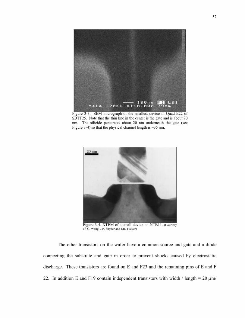
57
Chapter 1.
Figure 3-3. SEM micrograph of the smallest device in Quad E22 of SBTT25. Note that the thin line in the center is the gate and is about 70 nm. The silicide penetrates about 20 nm underneath the gate (see Figure 3-4) so that the physical channel length is ~35 nm.
Figure 3-4. XTEM of a small device on NTB11. (Courtesy of C. Wang, J.P. Snyder and J.R. Tucker)
The other transistors on the wafer have a common source and gate and a diode
connecting the substrate and gate in order to prevent shocks caused by electrostatic
discharge. These transistors are found on E and F23 and the remaining pins of E and F
22. In addition E and F19 contain independent transistors with width / length = 20 µm/
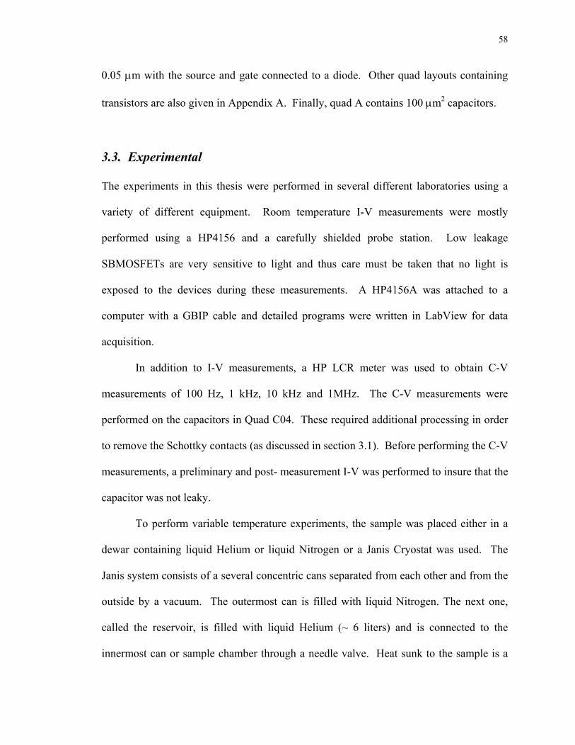
58
0.05 µm with the source and gate connected to a diode. Other quad layouts containing
transistors are also given in Appendix A. Finally, quad A contains 100 µm2 capacitors.
3.3. Experimental
The experiments in this thesis were performed in several different laboratories using a
variety of different equipment. Room temperature I-V measurements were mostly
performed using a HP4156 and a carefully shielded probe station. Low leakage
SBMOSFETs are very sensitive to light and thus care must be taken that no light is
exposed to the devices during these measurements. A HP4156A was attached to a
computer with a GBIP cable and detailed programs were written in LabView for data
acquisition.
In addition to I-V measurements, a HP LCR meter was used to obtain C-V
measurements of 100 Hz, 1 kHz, 10 kHz and 1MHz. The C-V measurements were
performed on the capacitors in Quad C04. These required additional processing in order
to remove the Schottky contacts (as discussed in section 3.1). Before performing the C-V
measurements, a preliminary and post- measurement I-V was performed to insure that the
capacitor was not leaky.
To perform variable temperature experiments, the sample was placed either in a
dewar containing liquid Helium or liquid Nitrogen or a Janis Cryostat was used. The
Janis system consists of a several concentric cans separated from each other and from the
outside by a vacuum. The outermost can is filled with liquid Nitrogen. The next one,
called the reservoir, is filled with liquid Helium (~ 6 liters) and is connected to the
innermost can or sample chamber through a needle valve. Heat sunk to the sample is a

59
thermometer and heater that are controlled by a LakeShore 330 temperature controller.
Obtaining a stable temperature between 4K and 300 K is thus an art in adjusting the
vapor flow from the reservoir, adjusting the pressure in the sample chamber and adjusting
the heater. The variable temperature measurements were automated by connecting the
LakeShore to a computer.
The wires of the header in the cryostat are connected to a 19-pin connector that is
subsequently attached to 16 coaxial cables. The four cables connected to the device then
went into a coaxial to triaxial converter box and then into either the HP4156B or
HP4145B Semiconductor Parameter Analyzer (SPA). The SPAs were grounded to a
water pipe and the noise of the system was checked using a resistor and a Dynamic
Signal Analyzer (HP3581). The noise level varied from ± 10 - ±50 µV depending on the
‘cleanliness’ of the cables. The frequency spectrum exhibited only 1/f noise. In addition
to the SPAs, a DC Voltage source (Yokogawa 3187) was sometimes used to increase the
voltage resolution of the gate. During measurements, the currents of the source, drain,
gate and substrate were routinely monitored to ensure that the gate was not leaky and that
there were no shorts.
Random telegraph signal was measured using the ‘sample mode’ of the
HP4156b. This model allows one to obtain the current as a function of time. These
measurements could not be performed on the HP4145b because the sample mode does
allow a high enough measurement resolution. Using the HP4156b the time between each
measurement point could be varied from about 500 µsec to 1 sec. These measurements
are complicated by the design of the HP4156b, which does not necessarily measure at the
specified interval if the interval is too short to accurately determine the current.
60
Finally, measurements in a magnetic field were also performed using a homemade
insert into the dilution refrigerator magnet. The superconducting magnet varies in field
from 0-8 T at 4 K and can reach 11 T at 2.2 K. In the measurements performed in the
magnet, it was sometimes essential to have the lower temperature, although not necessary
to have the higher fields. Pumping on the magnet is performed by pumping on a lambda
plate, which allows for more efficient pumping of the bath.
Chapter 4
Device Operation of the SBMOSFET
Device operation of the SBMOSFET was briefly introduced in Chapter 1, and in this
chapter the discussion is extended. In 4.1 we introduce a simple circuit that models the
SBMOSFET and intuitively captures the device behavior. Section 4.2 discusses the band
bending at the metal/semiconductor interface as a function of gate bias. The transport
limits of the different current regimes at various temperatures and gate bias are explored
in Section 4.3. We then focus on the sub-threshold and ‘on’ state regimes in Section 4.4
and 4.5. Finally, Section 4.6 considers an anomalous leakage current commonly found in
these devices.
4.1. Simple Circuit Model
Consider a metal/semiconductor/metal structure with all of the contacts at 0V (Figure 4-
1a). This structure has been used to create a barrier injection and transit time
(BARRITT) diode used for low power microwave applications such as local oscillators.
(Sze 1981, p. 566). For useful device operation, the source and drain regions must be
overlapping, a condition known as ‘reach-through’ that we will consider in Chapter 5.

62
BARRITT diodes are only useful in the 30-50 GHz range but are low power (1-10 mW)
compared to their high-power (1-5 W) GaAs and Si IMPATT cousins (Sze 1998,
Chapter 6). More recently Resonant Tunneling Diodes (RTDs) and Quantum Well
Injection Transit Time (QWITTs) devices have been increasingly used for this range and
power level (Kelly 1995, Chapter 17).
Efm Efs
qφibn qψbi
Ev
Ec
qφibp
a)
Vds
Rdbch Rch Rsb
Rdbsub
Rsub
Rsubb
b)
Figure 4-1. a) The equilibrium band diagram of a SBMOSFET. b) An effective circuit diagram showing all possible current paths with the different components labeled as simple resistors. Note that the gate effectively makes Rdbch, Rch and Rsb variable resistors.
The BARRITT diode has essentially the same structure as a SBMOSFET except
that a gate is formed above the semiconductor in the latter, which allows the band

63
bending to be altered either allowing or inhibiting current flow. First consider the MSM
structure in terms of a circuit diagram where the barriers, channel and substrate are
modeled as resistors (Figure 4-1b). There are four possible paths of current flow. Ideal
SBMOSFET behavior follows the path in which the majority of the current flows from
the source barrier (Rsb) into the channel (Rch) and then into the drain (Rdb).
At Vg = 0, both Rsb and Rdbsub must be large enough so that as |Vds| is increased,
the reverse saturation current will be very small and therefore no current will flow into
the channel or into the substrate. The Vds value at operation must therefore be small
enough so that the reverse saturation current meets the design criteria for the minimum
leakage current. With increasing gate bias, the Vds will be predominantly dropped at the
largest of the three resistors (Rdbch, Rch, Rsb). If the Schottky Barriers (Rdbch, Rsb) limit the
current, then the large resistance of the reverse bias source barrier will dominate. The
current transport mechanism at the metal/semiconductor contact will depend on the
temperature and on the gate bias. Previous work on PtSi/Si Schottky barriers indicates
that at room temperature thermionic emission dominates when the surface is n-type and
diffusion dominates when the surface is p-type (Andrews 1970a; Chin 1993). Later in
this chapter, we investigate the relative magnitudes of these components as a function of
gate bias.
Deviations from the ideal are due to the other possible current paths. The
dominant cause of the leakage has to do with the band bending near the source and drain
contacts, which can vary substantially. For instance, the band bending underneath the
gate is large and negative (|ψib| ~ φibn) at Vg = 0, goes through zero as the surface is
inverted, and then increases in strong inversion (|ψib| ~ φibp). These cases were depicted
64
in Figure 1-1 and are reconsidered in greater detail in Figure 4-4. Meanwhile, there is a
part of the contact that does not experience any influence of the gate electrode and is
therefore described simply by the standard metal/semiconductor theory explained in
Chapter 2. There is also the possibility that strong fields exist at any sharp edges that
have resulted from fabrication imperfections and effectively change the band bending
and/or the intrinsic barrier height. For simplicity, we assume in Figure 4-1b that the
Schottky barrier of the drain that is under the influence of the gate can be incorporated
into a resistor Rdbch and that part that is not affected into a resistor Rdbsub. This
assumption is kept until we consider device scaling in Chapter 5. Note that although the
same configuration exists at the source contact, there should be no current flow between
the source and substrate since they are at the same potential.
It is useful to consider the extreme non-ideal case in which Rdbch is very large but
Rdsub is small at Vg = 0. This arises, for instance, when SBMOSFETs are fabricated on a
p-type substrate instead of an n-type substrate and such devices were used in the quantum
interference measurements. Before the surface is accumulated, transport outside the
channel will dominate because of the low resistance substrate and thus a large sub-
threshold leakage current will be observed. Subsequently, the carriers will travel through
both the channel, which has a very small injection area, and the substrate in which the
injection area is much larger. In addition to the substantial off current, the substrate
leakage will therefore also prevent current saturation. It is only when the temperature is
sufficiently reduced so that thermionic emission/diffusion is not the dominant factor that
the transport in the channel can fully be separated from the sub-surface leakage current.
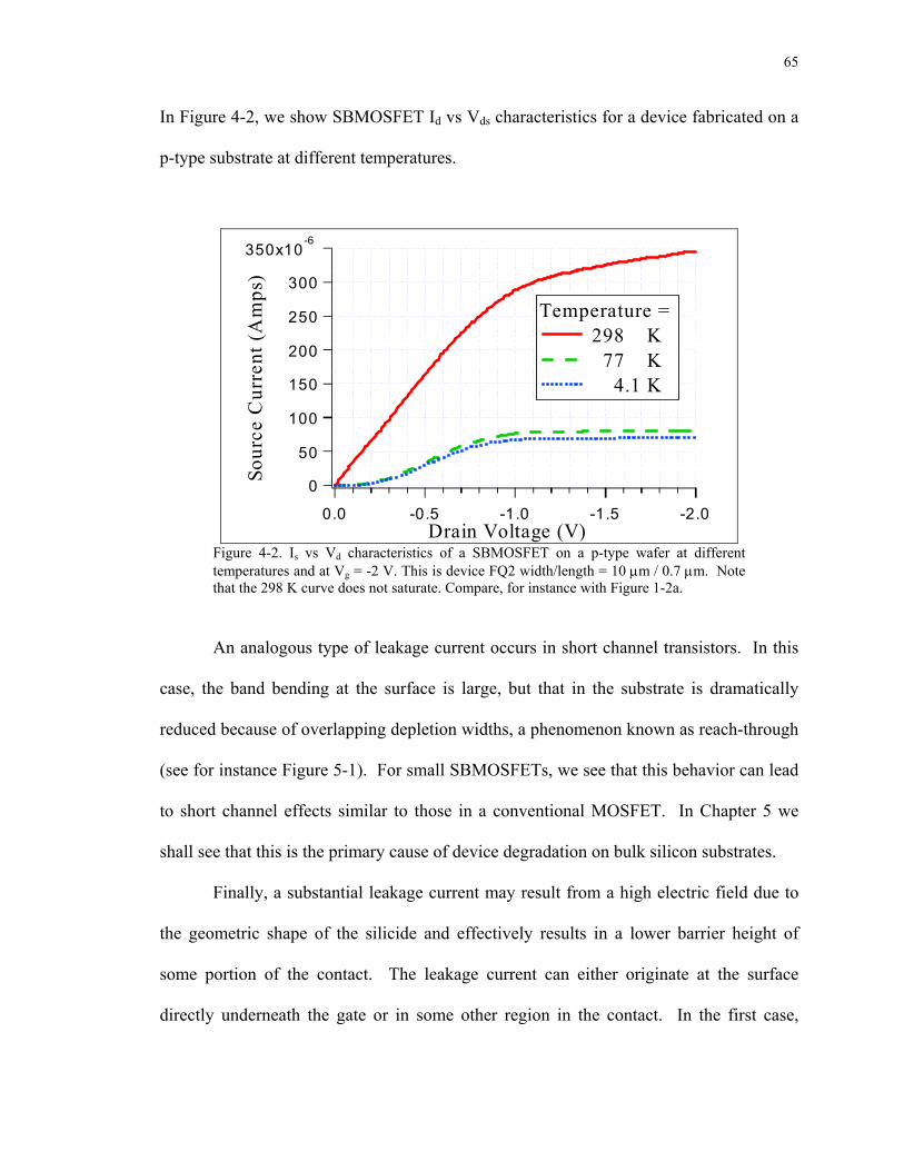
65
In Figure 4-2, we show SBMOSFET Id vs Vds characteristics for a device fabricated on a
p-type substrate at different temperatures.
350x10-6
300
250
200
150
100
50
0Sour
ce C
urre
nt (A
mps
)
-2.0-1.5-1.0-0.50.0Drain Voltage (V)
Temperature = 298 K 77 K 4.1 K
Figure 4-2. Is vs Vd characteristics of a SBMOSFET on a p-type wafer at different temperatures and at Vg = -2 V. This is device FQ2 width/length = 10 µm / 0.7 µm. Note that the 298 K curve does not saturate. Compare, for instance with Figure 1-2a.
An analogous type of leakage current occurs in short channel transistors. In this
case, the band bending at the surface is large, but that in the substrate is dramatically
reduced because of overlapping depletion widths, a phenomenon known as reach-through
(see for instance Figure 5-1). For small SBMOSFETs, we see that this behavior can lead
to short channel effects similar to those in a conventional MOSFET. In Chapter 5 we
shall see that this is the primary cause of device degradation on bulk silicon substrates.
Finally, a substantial leakage current may result from a high electric field due to
the geometric shape of the silicide and effectively results in a lower barrier height of
some portion of the contact. The leakage current can either originate at the surface
directly underneath the gate or in some other region in the contact. In the first case,

66
current flows from Rsb into the drain because the substrate is less n–type than the surface.
(Recall that the n-type Poly silicon gate causes an accumulation at Vg = 0.) If, on the
other hand, the source of the leakage current is not underneath the gate then the current
will flow directly from Rdbsub into Rsub. Some of the wafers we received from National
Semiconductor did exhibit large anomalous leakage currents of this nature and this is
investigated in Section 4.6.
4.2 Band Bending at the Metal/Semiconductor Interface
We assume that the leakage current in the conduction band is negligible and therefore
that the current is due to carriers in the valence band. At Vg = 0, holes see an ‘effective
barrier’ ψpeff that is due to the intrinsic barrier φibp and the band bending at the
metal/semiconductor surface ψbs:
peff ibp bsψ φ ψ= + (4.1)
The band bending (equation 2.6) can be obtained using the surface concentration psurf
from an analysis of the MOS capacitor.
In order to use the surface concentration developed in Chapter 2, we must assume
that the surface is non-degenerate and quantum mechanical effects can be neglected. In
fact, the graphs in Figure 2-8, indicate that at 300 K the surface is degenerate at Vg = -1.6
V. To verify this method, we use the Silvaco simulator to obtain the carrier
concentration. In Figure 4-3 we compare the simulation from Chapter 2 with two
simulations run on Silvaco’s Atlas simulator, and we see that the simulation from Chapter
2 is inaccurate in the strong inversion regime. We will therefore only use that method
when we discuss the sub-threshold regime, and otherwise the carrier concentrations from

67
Silvaco are used. We can vary the temperature of the simulations in Silvaco, but
typically there are convergence problems for T < 150 K.
1020
1015
1010
105
Sur
face
Con
cent
ratio
n (c
m-3
)
-2.0-1.5-1.0-0.50.0
Gate Voltage (V)
Silvaco Simulation 1 Silvaco Simulation 2 Igor Simulation
Figure 4-3. Surface concentrations obtained from the Silvaco simulator Atlas and the method described in Chapter 2. The squares used Boltzmann statistics and the circles used the quantum moments method and Fermi-Dirac statistics. The Igor simulation (triangles) was obtained by numerically iterating Equation (2.20).
The band bending is best described by examining the schematic diagram in Figure
4-4 where it is seen that two equations are necessary: one when the bands bend up and
another when they bend down. The transition point (Figure 4-4c) is of particular
importance, and occurs when the hole concentration at the surface ps is:
( )exp 2s i ip gqp n E
kTφ = − −
(4.2)
This is a universal value in that it only depends on the barrier height and on the
temperature. This transition does not occur in a conventional MOSFET, where the large

68
qφibn qψbs
Ef - Ei
a) ln2surfg
bs ibni
nkTEq n
ψ φ
= − +
φpeff
b) ln ln2 2surf surfg g
bs ibp ibni i
n nkT kTE Eq n q n
ψ φ φ
= − + = − +
c) bs ibpψ φ=
Ei - Ef
d) ln2
g surfbs ibp
i
E nkTq n
ψ φ
= − −
Figure 4-4. Schematic of the band bending as a function of gate bias. a) The surface is n-type, b) the surface is inverted but the band bending is still positive, c) band bending at the transition point, and d) the band bending becomes negative.

69
barriers caused by p-n junctions are reduced until current flow is facilitated, but never
reverse their direction. At room temperature, ps = 1. 7 X 1016 cm-3, which occurs at Vg =
–0.98 V.
4.3 Current Transport Limits
Transport at the barrier can occur by thermionic emission, thermal assisted tunneling or
direct tunneling. From Figure 4-4, it is easy to see that until ψbs goes through zero, only
thermionic emission is possible. The limits separating each of these regimes are given in
Padovani (1966). Our goal in this section is to determine the dominant transport
mechanism for different gate bias at room temperature. We note although the channel is
never degenerate in the practical range of gate bias (0 to –2 V); the Fermi level does
come within kT/q of the valence band and thus direct tunneling is a possibility.
Of particular importance is the reduced energy E00 given by:
00 2 *s
NEmε
= , (4.3)
which varies as a function of gate bias. In order to determine E00 as a function of gate
bias, we use the surface concentration obtained from Silvaco simulations.
The limit between thermionic emission and thermal assisted tunneling in the
reverse bias direction is given by:
( )( )
20000
300
cosh32 sinhds b
E kTEq V qE kT
φ ξ> + + (4.4)
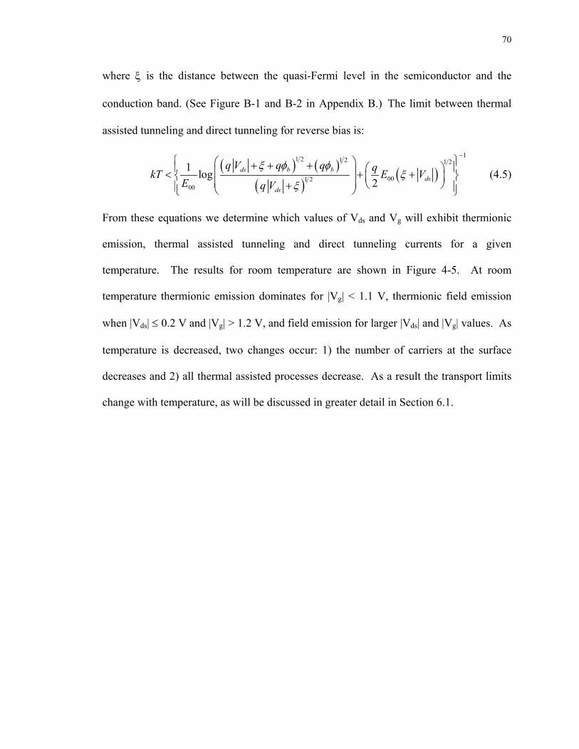
70
where ξ is the distance between the quasi-Fermi level in the semiconductor and the
conduction band. (See Figure B-1 and B-2 in Appendix B.) The limit between thermal
assisted tunneling and direct tunneling for reverse bias is:
( ) ( )( )
( )11 2 1 2 1 2
001 200
1 log2
ds b bds
ds
q V q q qkT E VE q V
ξ φ φξ
ξ
− + + + < + + +
(4.5)
From these equations we determine which values of Vds and Vg will exhibit thermionic
emission, thermal assisted tunneling and direct tunneling currents for a given
temperature. The results for room temperature are shown in Figure 4-5. At room
temperature thermionic emission dominates for |Vg| < 1.1 V, thermionic field emission
when |Vds| ≤ 0.2 V and |Vg| > 1.2 V, and field emission for larger |Vds| and |Vg| values. As
temperature is decreased, two changes occur: 1) the number of carriers at the surface
decreases and 2) all thermal assisted processes decrease. As a result the transport limits
change with temperature, as will be discussed in greater detail in Section 6.1.
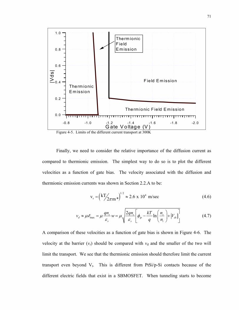
71
1.0
0.8
0.6
0.4
0.2
0.0
|Vds
|
-2.0-1.8-1.6-1.4-1.2-1.0-0.8G ate V o ltag e (V )
Therm ionic F ie ld E m iss ion
Therm ionic E m iss ion
F ie ld E m iss ion
Therm ionic F ie ld E m iss ion
Figure 4-5. Limits of the different current transport at 300K
Finally, we need to consider the relative importance of the diffusion current as
compared to thermionic emission. The simplest way to do so is to plot the different
velocities as a function of gate bias. The velocity associated with the diffusion and
thermionic emission currents was shown in Section 2.2.A to be:
( )1/ 24
rkTv 2.6 x 10 m/sec2 m*π= ≈ (4.6)
max2 lns s s
d ip dss s i
qn qn nkTv w Vq n
µ µ µ φε ε
≈ = = − +
E (4.7)
A comparison of these velocities as a function of gate bias is shown in Figure 4-6. The
velocity at the barrier (vr) should be compared with vd and the smaller of the two will
limit the transport. We see that the thermionic emission should therefore limit the current
transport even beyond Vt. This is different from PtSi/p-Si contacts because of the
different electric fields that exist in a SBMOSFET. When tunneling starts to become

72
important, the drift/diffusion component need no longer be considered because carriers
do not traverse the depletion widths, but tunnel through them.
2.0x10⁶
1.5
1.0
0.5
0.0
Vel
ocity
(m/s
ec)
-2.0-1.8-1.6-1.4-1.2-1.0Gate Voltage (V)
Thermal velocity Drift Velocity
Figure 4-6. Comparison of thermal velocity vs drift velocity as a function of gate bias where we have assumed a mobility of ~160 cm2/V-sec.
4.4. The Sub-threshold Regime
It is convenient to separate the ‘on’ and ‘off’ states of the SBMOSFET using the
transition point defined by equation (4.2). In particular, the sharp sub-threshold swing in
SBMOSFETs is due to the effective barrier lowering before the bands invert. The
transition point from Section 4.2, is thus the ‘threshold voltage’ of the SBMOSFET, as
compared to the traditional ‘threshold voltage’ of a conventional MOSFET, which occurs
at the onset of strong inversion. This distinction nicely separates the transport regimes: in
the sub-threshold only thermionic emission or ‘classical transport’ occurs, while in the
‘on’ state both ‘classical’ and ‘quantum mechanical’ transport may exist.
Defining the threshold voltage as the transition point has several consequences for
designing SBMOSFETs. Ideally, one could modify the substrate doping to be exactly the
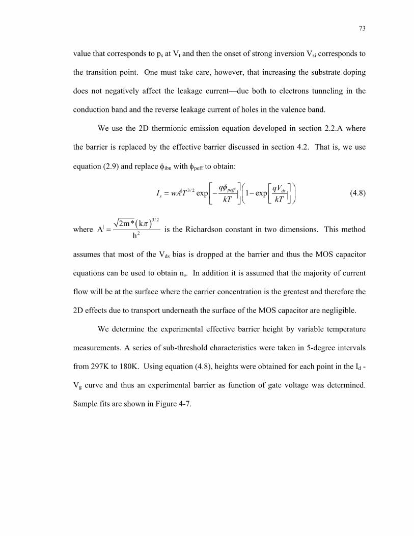
73
value that corresponds to ps at Vt and then the onset of strong inversion Vsi corresponds to
the transition point. One must take care, however, that increasing the substrate doping
does not negatively affect the leakage current—due both to electrons tunneling in the
conduction band and the reverse leakage current of holes in the valence band.
We use the 2D thermionic emission equation developed in section 2.2.A where
the barrier is replaced by the effective barrier discussed in section 4.2. That is, we use
equation (2.9) and replace φibn with φpeff to obtain:
| 3/ 2 exp 1 expφ = − −
peff dss
q qVI wATkT kT
(4.8)
where ( )3/ 2|
2
2m* kA
hπ
= is the Richardson constant in two dimensions. This method
assumes that most of the Vds bias is dropped at the barrier and thus the MOS capacitor
equations can be used to obtain ns. In addition it is assumed that the majority of current
flow will be at the surface where the carrier concentration is the greatest and therefore the
2D effects due to transport underneath the surface of the MOS capacitor are negligible.
We determine the experimental effective barrier height by variable temperature
measurements. A series of sub-threshold characteristics were taken in 5-degree intervals
from 297K to 180K. Using equation (4.8), heights were obtained for each point in the Id -
Vg curve and thus an experimental barrier as function of gate voltage was determined.
Sample fits are shown in Figure 4-7.

74
-20
-18
-16
-14
Log
of S
ourc
e C
urre
nt
5 .0 x10 -3 4 .54.03.51/Temperature(K-1
)
297 265 239 218 200 185
Vds=- -0 .150 V -0 .015 V -0 .005 V
Temperature (K)
I = A A* exp(-qφB / kT)
Figure 4-7. Determination of the Schottky barrier for fixed Vg and Vds.
The goal in fitting the barrier heights is to obtain the effective barrier as a function
of gate bias. This will allow us to determine the intrinsic barrier height of the inverted
PtSi/Pt contact and obtain the leakage current as function of effective barrier, which are
both important design parameters. Several problems were encountered in fitting the data.
First, the current decreases exponentially with temperature and therefore the fits are
inaccurate for small values of |Vg| where we are limited by the current resolution of the
HP4156. An illustration of this effect is shown in Figure 4-8. In this graph, the fit in the
295 K to 240 K range reaches a peak at Vg = -0.65 V and corresponds to the Vg value at
which the smallest current used in this fit begins to increase. Similarly the fit between
185 and 235 exhibits a peak at a larger |Vg| value, which also corresponds to the Vg value
at which the 185 K current begins to increase. The fits at |Vg| values smaller than the
maximum barrier height fit, are thus distorted by the very low current levels of the
transport characteristics.
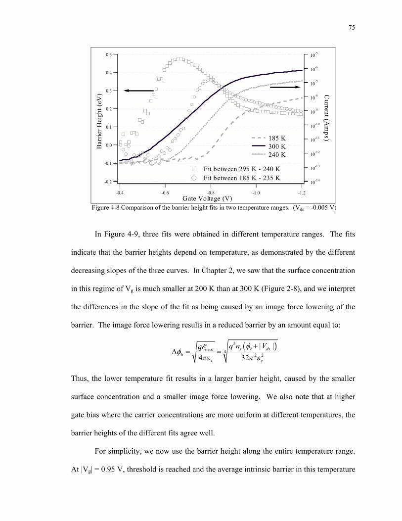
75
10-14
10-13
10-12
10-11
10-10
10-9
10-8
10-7
10-6
10-5
Current (A
mps)
-1.2-1.0-0.8-0.6-0.4Gate Voltage (V)
0.5
0.4
0.3
0.2
0.1
0.0
-0.1
-0.2
Bar
rier H
eigh
t (eV
)
185 K 300 K 240 K
Fit between 295 K - 240 K Fit between 185 K - 235 K
Figure 4-8 Comparison of the barrier height fits in two temperature ranges. (Vds = -0.005 V)
In Figure 4-9, three fits were obtained in different temperature ranges. The fits
indicate that the barrier heights depend on temperature, as demonstrated by the different
decreasing slopes of the three curves. In Chapter 2, we saw that the surface concentration
in this regime of Vg is much smaller at 200 K than at 300 K (Figure 2-8), and we interpret
the differences in the slope of the fit as being caused by an image force lowering of the
barrier. The image force lowering results in a reduced barrier by an amount equal to:
( )3max 4
2 2
| |4 32
s b dsb
s s
q n Vq φφ
πε π ε+
∆ = =E
Thus, the lower temperature fit results in a larger barrier height, caused by the smaller
surface concentration and a smaller image force lowering. We also note that at higher
gate bias where the carrier concentrations are more uniform at different temperatures, the
barrier heights of the different fits agree well.
For simplicity, we now use the barrier height along the entire temperature range.
At |Vg| = 0.95 V, threshold is reached and the average intrinsic barrier in this temperature
76
range is found to be ~ 0.22 eV. From the discussion above, however, the barrier may be
< 0.19 eV at room temperature due to the image force potential associated with the larger
carrier concentration. For |Vg| > 0.95 V, the experimental barrier continues to decrease,
but with a different slope than previously. Fitting in this regime is much more
complicated and one cannot a priori use the thermionic emission equation. In particular,
we saw in section 4.3 that field emission should be the dominant current transport
mechanism at the barrier. Despite this, the barrier heights for |Vg| > |Vt| do in fact fit well
to the thermionic emission equation. This is discussed in greater detail in the next
section.
0.5
0.4
0.3
0.2
0.1
0.0
Bar
rier (
eV)
-2.0-1.8-1.6-1.4-1.2-1.0-0.8-0.6Gate Voltage (V)
Fit between 185 K - 295 K Fit between 240 K - 295 K Fit between 185 K - 235 K
Figure 4-9. Comparison of barrier fits (with error bars) as a function of gate bias for different temperature regimes with error bars. The fits are taken for Vds = -0.005 V. Note that the higher temperature regime has a better resolution at smaller |Vg|.

77
0 .6
0 .5
0 .4
0 .3
0 .2
0 .1
0 .0
Bar
rier H
eigh
t (eV
)
-2 .0-1 .8-1 .6-1 .4-1 .2-1 .0-0 .8-0 .6-0 .4G a te V o lta g e (V )
1 0-1 2
1 0-1 0
1 0-8
1 0-6
1 0-4
Current (A
mps/µm
)V d s = -0 .0 5 V
E x p e rim e n ta l B a rrie r S im u la te d B a rrie r C u rre n t @ 3 0 0 K
Figure 4-10. Comparison of the effective barrier height obtained by simulation (solid line) and experimental measurements (dashed line) at Vds = -0.05 V. For convenience we include the 300 K current.
Using the surface concentrations from the MOS capacitor, we model the effective
barrier (equation 4.1) and compare it with the one obtained experimentally. The
simulated barrier is the solid line in Figure 4-10. Within the resolution of the
measurement (|Vg| > 0.8 V) the agreement between the two barrier heights is quite good
in the sub-threshold regime. For |Vg| < 0.8 V, where the resolution of the current does
not allow the determination of the true effective barrier, the simulated barrier can provide
an estimate. When the effective barrier height is plotted on the same graph as the sub-
threshold current, we obtain the leakage current corresponding to a given barrier height.
For instance, an initial effective barrier height of 0.6 eV corresponds to ~ pA/µm of
current and thus is sufficient to meet the minimum off state leakage in a practical device.
We could then adjust the work-function of the gate and/or the substrate doping so that the
Vt is shifted to a different value of Vg, keeping in mind that the effective barrier in the off
78
state must be ~0.6 eV. This correspondence between effective barrier height and leakage
current is also valuable for silicidation of conventional MOSFETs, where ultra-shallow
silicided junctions can lead to large leakage currents (Kang 2000).
4.5. Device Behavior in the On State In this section we describe the device operation in the ‘on’ state, in which the effective
barrier has been reduced to the intrinsic barrier height. Analogous to a conventional
MOSFET, we consider transport in two regimes of Vds bias: the linear regime and the
saturation regime. Ideally, the channel resistance and not the Schottky barrier limit the
transport. We therefore modify the conventional MOSFET equations in order to capture
the influence of the Schottky Barrier by assuming that it acts as an additional series
resistance. The validity of this method is then discussed.
Linear Regime
We consider values of |Vds| << Vt. From Section 4.3, we expect thermionic emission to
dominate for |Vg| < 1.1 V and field emission when |Vds| > 0.2 V and |Vg| > 1.2 V. We
explain the change in the current after φpeff = φibp as due to image force lowering of the
barrier and the decrease in channel resistance. Since the channel and the barriers are in
series, we first capture the effect of the barrier using a parasitic resistance for the source
and drain and the conventional MOSFET equation in the linear regime:
( )( )d eff ox g si d t dWI C V V V R IL
µ= − − (4.9)
where Vsi is the onset of strong inversion, and we have assumed that Vds is negative and
Rt is the total effective series resistances at the source and drain

79
If the barrier dominates the transport, Rt is a function of gate bias, if it does not
then Rt is approximately constant and the change in current is due predominantly to the
channel resistance. Since in this device Vsi < Vt, Rt is a strong function of gate bias until
Vt because of the change in the effective barrier φpeff. Once threshold is reached, the
transconductance will reach a ‘local’ maximum because φpeff no longer changes as a
function of gate voltage. Subsequently, the increase in current is related either to image
force lowering, increased conduction at the Schottky Barrier (due to tunneling) or to
transport in the channel.
10- 12
10- 10
10-8
10-6
Sour
ce C
urre
nt (
A)
-2 .0-1.5-1.0-0.50.0
G ate V o ltage (V )
-15x10-6
-10
-5
0
Transconductance (S)
W / L = 2 0 µ m / 1 .7 µ mVds = -0 .0 5 0 @ T = 2 9 5 K
Figure 4-11. Sub-threshold current and transconductance of an SBMOSFET. Note that unlike a
conventional MOSFET, after Vt is reached the transconductance continues to increase.
The transconductance and current are shown in Figure 4-11. This behavior is
different from a conventional MOSFET, in which the transconductance reaches a peak at
threshold and then decreases with increasing |Vg| due to surface roughness scattering. In

80
this case, we believe that the transconductance increases because of increased transport at
the barrier due to tunneling.*
To justify equation (4.9) we first consider the thermionic emission equation (2.9):
| 3/ 2 exp exp 1b bd
q qVI A wTkT kTφ = − −
(4.10)
where Vb is the voltage dropped across the barrier and is related to Vds by: ds b chV V V= + .
If we assume that 1bqVkT
then we can expand this to:
| 1/ 2 expb b bd
t
qV q VI A wTk kT R
φ = − =
(4.11)
where 1
| 1/ 2 1 exp bt
qR A wT qkkTφ
−− = −
. We assume that the 2D Richardson constant
without corrections for optical phonon scattering and quantum mechanical reflection, and
estimate the smallest series resistance possible. At room temperature this is Rt = 54 Ω.
While this value is very small, we know from the discussion in Chapter 2 that A| does not
include the effects of optical phonon scattering and quantum mechanical reflections. By
comparison with the 3D Richardson constant, this value should be ~ 2.5 times larger or
~136 Ω.
* We note that this increase is not due to leakage from the gate. In particular the gate current is < 1 pAmp in this device.
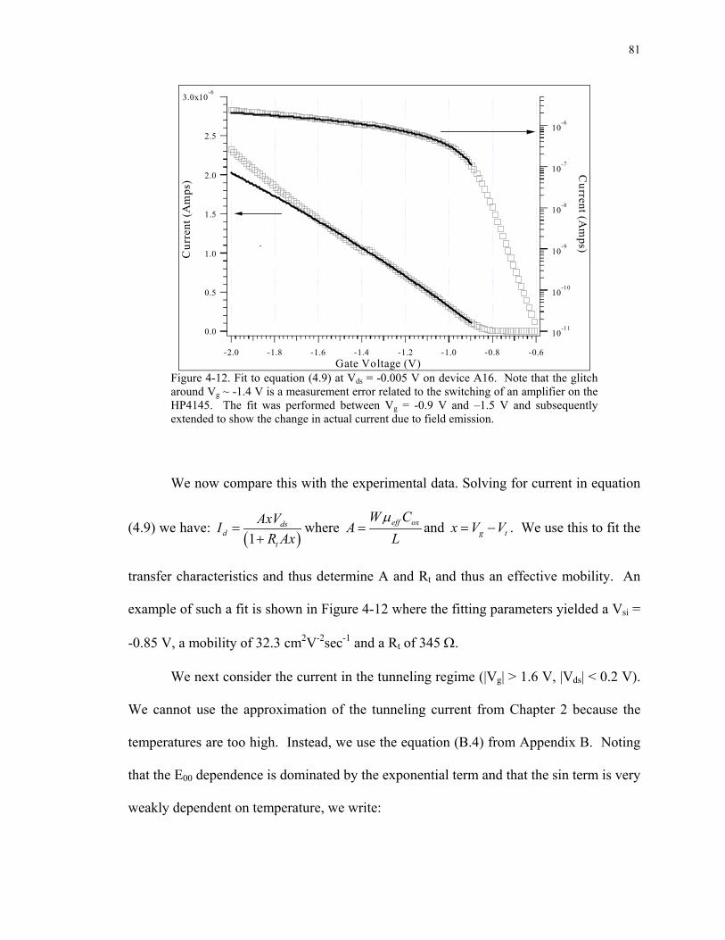
81
3.0x10⁻⁶
2.5
2.0
1.5
1.0
0.5
0.0
Cur
rent
(Am
ps)
-2.0 -1.8 -1.6 -1.4 -1.2 -1.0 -0.8 -0.6Gate Voltage (V)
10-11
10-10
10-9
10-8
10-7
10-6
Current (A
mps)
Figure 4-12. Fit to equation (4.9) at Vds = -0.005 V on device A16. Note that the glitch around Vg ~ -1.4 V is a measurement error related to the switching of an amplifier on the HP4145. The fit was performed between Vg = -0.9 V and –1.5 V and subsequently extended to show the change in actual current due to field emission.
We now compare this with the experimental data. Solving for current in equation
(4.9) we have: ( )1
dsd
t
AxVIR Ax
=+
where eff oxW CA
Lµ
= and g tx V V= − . We use this to fit the
transfer characteristics and thus determine A and Rt and thus an effective mobility. An
example of such a fit is shown in Figure 4-12 where the fitting parameters yielded a Vsi =
-0.85 V, a mobility of 32.3 cm2V-2sec-1 and a Rt of 345 Ω.
We next consider the current in the tunneling regime (|Vg| > 1.6 V, |Vds| < 0.2 V).
We cannot use the approximation of the tunneling current from Chapter 2 because the
temperatures are too high. Instead, we use the equation (B.4) from Appendix B. Noting
that the E00 dependence is dominated by the exponential term and that the sin term is very
weakly dependent on temperature, we write:
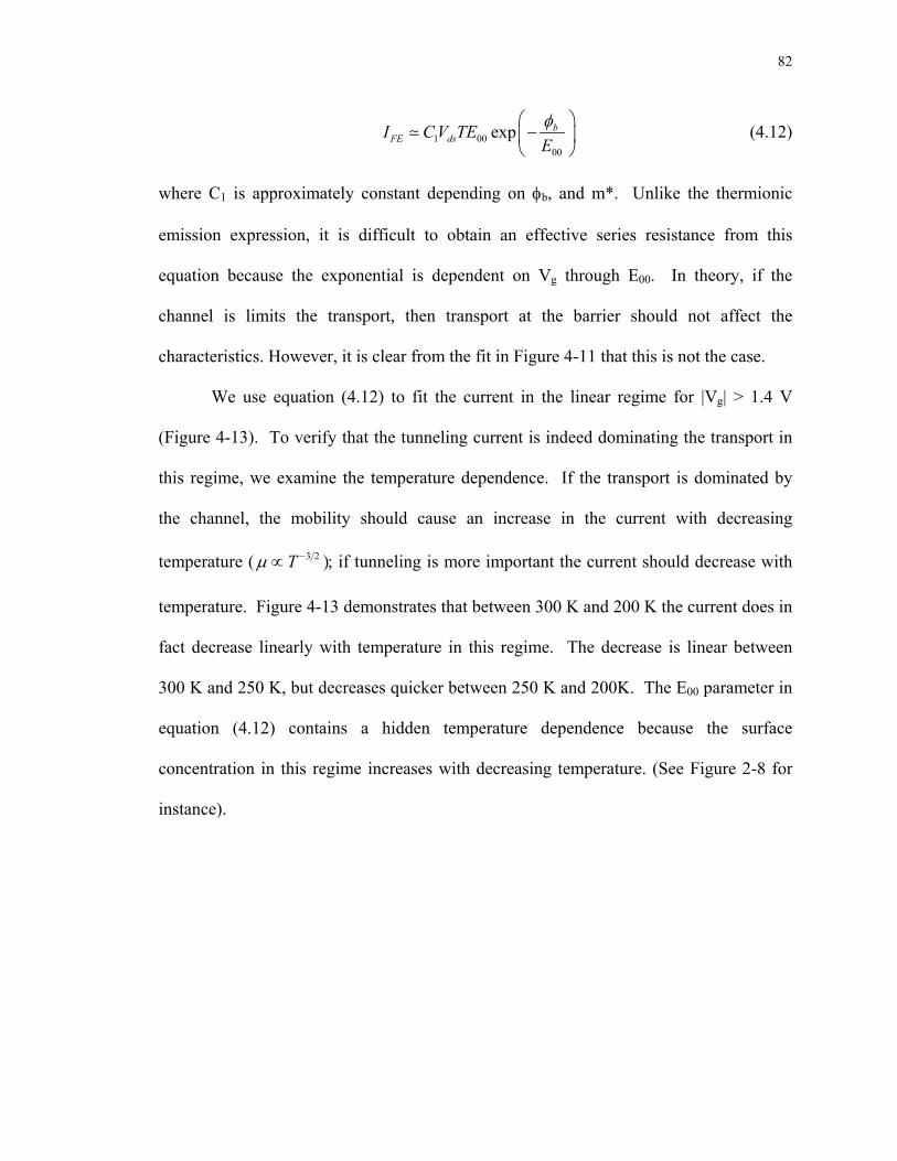
82
1 0000
exp bFE dsI C V TE
Eφ
−
(4.12)
where C1 is approximately constant depending on φb, and m*. Unlike the thermionic
emission expression, it is difficult to obtain an effective series resistance from this
equation because the exponential is dependent on Vg through E00. In theory, if the
channel is limits the transport, then transport at the barrier should not affect the
characteristics. However, it is clear from the fit in Figure 4-11 that this is not the case.
We use equation (4.12) to fit the current in the linear regime for |Vg| > 1.4 V
(Figure 4-13). To verify that the tunneling current is indeed dominating the transport in
this regime, we examine the temperature dependence. If the transport is dominated by
the channel, the mobility should cause an increase in the current with decreasing
temperature ( 3 2Tµ −∝ ); if tunneling is more important the current should decrease with
temperature. Figure 4-13 demonstrates that between 300 K and 200 K the current does in
fact decrease linearly with temperature in this regime. The decrease is linear between
300 K and 250 K, but decreases quicker between 250 K and 200K. The E00 parameter in
equation (4.12) contains a hidden temperature dependence because the surface
concentration in this regime increases with decreasing temperature. (See Figure 2-8 for
instance).
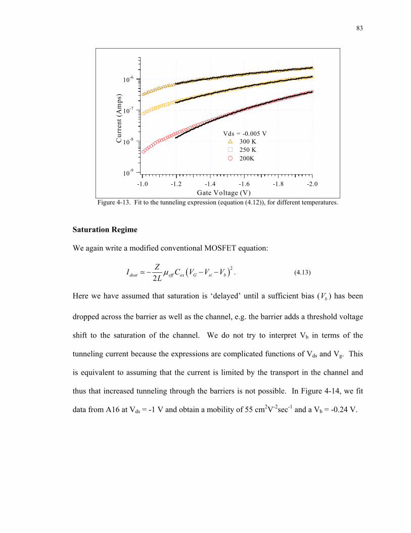
83
10-9
10-8
10-7
10-6
Cur
rent
(Am
ps)
-2.0-1.8-1.6-1.4-1.2-1.0Gate Voltage (V)
Vds = -0.005 V 300 K 250 K 200K
Figure 4-13. Fit to the tunneling expression (equation (4.12)), for different temperatures.
Saturation Regime
We again write a modified conventional MOSFET equation:
( )2
2dsat eff ox G si bZI C V V VL
µ− − − . (4.13)
Here we have assumed that saturation is ‘delayed’ until a sufficient bias ( bV ) has been
dropped across the barrier as well as the channel, e.g. the barrier adds a threshold voltage
shift to the saturation of the channel. We do not try to interpret Vb in terms of the
tunneling current because the expressions are complicated functions of Vds and Vg. This
is equivalent to assuming that the current is limited by the transport in the channel and
thus that increased tunneling through the barriers is not possible. In Figure 4-14, we fit
data from A16 at Vds = -1 V and obtain a mobility of 55 cm2V-2sec-1 and a Vb = -0.24 V.

84
250x10-6
200
150
100
50
0
Cur
rent
(Am
ps)
-2.0-1.8-1.6-1.4-1.2-1.0Gate Voltage (V)
Figure 4-14. Fit to equation (4.13) at Vds = -1V for Sample A16 width / length = 20 µm / 1.7 µm.
It should be noted that in these fits Vsi is assumed to be 0.85 V, which is calculated based
on an ideal MOS capacitor. In practice, one cannot disentangle the true MOS Vsi from the
effective threshold voltage Vsi + Vb ; all that can be said is that there is some shift.
We now consider a fit to the field emission equation (4.11). The fits for different
temperatures are shown in Figure 4-15. It is seen that the field emission captures the
transport better than the modified MOSFET equation. We therefore conclude that even
in the saturation regime, the Schottky barrier limits the current transport. This feature
shows up in the Id vs Vg transport characteristics by the larger increase in the saturation
current with Vg bias (Figure 1-2b).
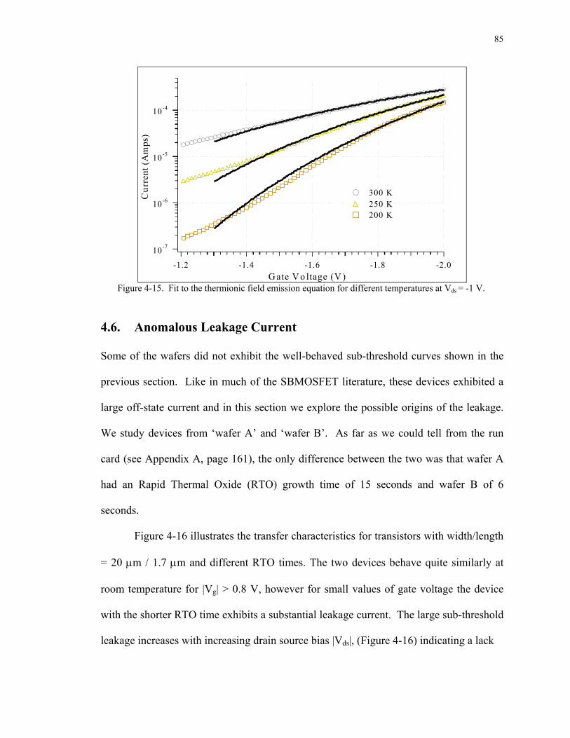
85
10-7
10-6
10-5
10-4
Cur
rent
(Am
ps)
-2.0-1.8-1.6-1.4-1.2G ate V o ltage (V )
300 K 250 K 200 K
Figure 4-15. Fit to the thermionic field emission equation for different temperatures at Vds = -1 V.
4.6. Anomalous Leakage Current
Some of the wafers did not exhibit the well-behaved sub-threshold curves shown in the
previous section. Like in much of the SBMOSFET literature, these devices exhibited a
large off-state current and in this section we explore the possible origins of the leakage.
We study devices from ‘wafer A’ and ‘wafer B’. As far as we could tell from the run
card (see Appendix A, page 161), the only difference between the two was that wafer A
had an Rapid Thermal Oxide (RTO) growth time of 15 seconds and wafer B of 6
seconds.
Figure 4-16 illustrates the transfer characteristics for transistors with width/length
= 20 µm / 1.7 µm and different RTO times. The two devices behave quite similarly at
room temperature for |Vg| > 0.8 V, however for small values of gate voltage the device
with the shorter RTO time exhibits a substantial leakage current. The large sub-threshold
leakage increases with increasing drain source bias |Vds|, (Figure 4-16) indicating a lack

86
10-12
10-10
10-8
10-6
Sou
rce
Cur
rent
(A
mps
)
-2.0-1.5-1.0-0.50.0Gate Voltage (V)
W / L = 20 µm/ 1.7 µmVds = -0.05
High Leakage Device Low Leakage Device
Figure 4-16 Room temperature transfer characteristics of the 6-second (60 A oxide) and the 15-second (100 A oxide) RTO devices. (Width/Length = 20 µm / 1.7 µm.)
10-12
10-11
10-10
10-9
10-8
10-7
10-6
10-5
10-4
10-3
Sour
ce C
urre
nt (A
mps
)
-2.0-1.5-1.0-0.50.0Gate Voltage (V)
Vds = -0.005 -0.015 -0.050 -0.150 -0.500
Figure 4-17 Room temperature transfer characteristics of the 6-second devices for different Vds values.
of saturation or soft breakdown in the reverse bias characteristics of the PtSi / n-type Si
Schottky barrier. This effect is common in reverse biased PtSi Schottky Barriers that are

87
fabricated without guard rings and is attributed to an ‘edge effect’ (Rideout and Crowell
1970). We now try to determine from where in the contact the leakage originates.
Figure 4-18 shows the absolute magnitude of the source, drain and substrate
currents. (Note that the substrate contact is not Ohmic, but consists of a PtSi contact
surrounded by a field oxide which allows the substrate to remain at the same potential as
the source without additional leakage current.) While in the high leakage devices, the
current in the off state predominantly flows from the drain to the substrate, in the low
leakage devices the current flows through the active device area. This indicates that the
leakage current may not be originating underneath the gate; an observation supported by
XTEMs of the channel in which different RTO times have similar Source/Drain contact
profiles under the gate (Wang 1998).
In Figure 4-19a we compare two different size devices and it is observed that the current
plateaus are approximately equal in magnitude. Because the plateau does not depend on
device size, is not affected by the applied gate voltage, and because the dominant current
in the off state flows between drain and substrate, the leakage current must originate at an
edge between the source/drain to substrate contacts. To further investigate the source of
this leakage, an Ohmic contact was formed to the bottom of the substrate so that the
forward bias curves and thus the ideality factors could be obtained (Figure 4-19b). While
the low leakage device exhibited a near perfect ideality of 1.006, the high leakage device
exhibited an ideality of 2.24.

88
10-12
10-10
10-8
10-6
10-4
|Cur
rent
| (A
)
-2.0-1.5-1.0-0.50.0
Gate Voltage (V)
Vds = -0.05 @ 300 K Source Current Drain Current Substrate Current
10-12
10-10
10-8
10-6
|Cur
rent
| (A
)
-2.0-1.5-1.0-0.50.0
Gate Voltage (V)
Vds = -0.05 V @ 300 K Source Current Drain Current Substrate Current
Figure 4-18. Room temperature |Id|, Is, Isub vs. Vg for the high leakage (a) and low leakage (b) devices.
Indications are that the leakage current originates at the edge of the contact
directly underneath the field oxide. In particular, the profile of the field oxide is
very sharp after the etch used to define the source/drain regions. The longer RTO
time used to form the sidewall spacers, allows for a rounding of the field oxide
edge. The profile of the PtSi around the field oxide is critically dependent upon
the field oxide’s edge profile, e.g. a slightly rounder field oxide corner will result

89
in a rounder PtSi corner. The longer RTO time resulting in a rounder field oxide
edge effectively eliminates the leakage from the contact edges underneath the
field oxide.
10-14
10-12
10-10
10-8
10-6
10-4So
urce
Cur
rent
(Am
ps)
-2.0-1.5-1.0-0.50.0
Drain Voltage (V)
Low L eakage Devices W / L =: 20 µ m/ 1.7 µm 10 µ m/ 0.7 µm
Anomalous Leakage Devices W / L = 20 µ m/ 1.7 µm 10 µ m/ 0.7 µm
Gate Voltage
a)
-25
-20
-15
-10
ln(I
)
0 .50 .40 .30 .20 .10 .0V o ltage (V )
L o w L e akage Subs trate , n = 1 .0 0 6 H igh L e akage Subs tr ate , n = 2 .2 7
b)
Figure 4-19 a)The sub-threshold curves of different size devices at Vds = -0.05 V. Note that the low leakage device characteristics scale with width, but the anomalous leakage plateaus do not. b) Forward bias characteristics of diodes from the wafers with the low and high leakage devices. The markers indicate experimental data and the solid lines the fit from which the ideality factor is extracted.
90
4.6 Concluding Remarks
In this chapter we have explored the device operation of the SBMOSFET in the 200 K –
300 K temperature range. We first introduced a simple circuit that allows a simplified
analysis based on lumping the different transport obstacles into a series of resistors. Next
we defined an effective barrier that consists of the intrinsic barrier and the band bending
at the metal/semiconductor surface. Where the effective barrier is reduced to the intrinsic
value, we define the threshold voltage of the SBMOSFET. Prior to sub-threshold, the
current transport is dominated by thermionic emission. In Section 4.4 we investigated the
sub-threshold behavior and were able to determine an experimental barrier height from
measurements taken at variable temperatures. We found that the change in surface
concentration with temperature causes the image force lowering and thus the barrier
height to vary substantially. Excellent agreement is found between the experimental and
simulated effective barrier heights and allows the determination of the off state leakage
for different effective barriers.
In Section 4.3 we discussed the different current transport mechanism limiting
carrier transport at the barriers. We found that for small |Vds| values, the current is limited
by thermionic and field emission, and by thermionic emission and thermal assisted
tunneling for larger values. While the conventional MOSFET equations can be used to
approximately describe the data, Section 4.5 showed that in general the current is limited
by the transport at the barrier. This is evidenced both by fitting the Id vs Vg curves and
by variable temperature measurements, which decrease with temperature. Finally, in
Section 4.6 we investigated an anomalous leakage current which can occur in

91
SBMOSFETs and which is caused by the large electric fields that can exist in the source
and drain contacts underneath the field oxide.
Chapter 5
Scaling of the SBMOSFET
In this chapter we first define the long channel, reach-through and flat-band regimes of
SBMOSFETs. The slight difference in terminology as compared to regular MOSFETs is
due to the BARRITT diode literature. In particular, what is normally called ‘punch-
through’ is termed ‘reach-through’. Although this may seem unnecessary, reach-through
does not necessarily mean that the device will not saturate or that the sub-threshold is
deteriorated. Instead, the onset of reach-through can be used as design criterion for the
smallest critical dimension. Because the band bending changes as a function of the
distance from the oxide, the device can be in several regimes at different depths. This is
essential in understanding the scaling of the experimental devices on wafer A. To
simplify the analysis we assume the simple resistor model considered in Section 4.1, and
show that the path through the substrate can be in the flat-band regime while the surface
is still well behaved.

93
5.1. Definition of Scaling Regimes
Based on earlier work on Metal-Semiconductor-Metal contacts (Sze 1971), we define
three scaling regimes for SBMOSFETs, as depicted in Figure 5-1. The regimes defined
in Sze’s original work were observed by varying the applied bias across a MSM junction,
not as is the case in this research by varying the length of the device. In Figure 5-1 the
scaling regimes are depicted in equilibrium for simplicity but that the band bending ψb
and thus the regimes will change as both Vds and Vg are varied. Note that since the
device operation involves inversion, the surface must always go through reach-through
and flat-band to turn on.
We assume the depletion approximation discussed in Chapter 2 and use equation
(2.5) for the depletion widths. In the long channel regime the sum of the depletion
widths at the source 2s s bW qNε ψ= and at the drain ( )2d s b dsW V qNε ψ= − are much
smaller than the channel length L (Figure 5-1a). Such devices are clearly well behaved
and can be accurately described by the analysis in Chapter 4.
At the onset of reach-through, the depletion widths at the source and drain are
equal to the channel length (Ws + Wd = L). For the moment, assume the length is much
larger than the two depletion widths at 0 bias and as |Vds| is increased reach-through
occurs. We can define the Vds value at this point as the reach-through voltage, VRT and
with some algebra it is found to be:
1/2RT FB FB bV = V - [4V ]ψ (5.1)
where
2
FBs
L qNV = 2ε
(5.2)

94
is the flat-band voltage, which will be discussed shortly. At the onset of this regime,
shown in Figure 5-1b, the band bending ψb and thus φpeff are the same as in the long
channel regime. However, subsequent increase in |Vds| will reduce the band bending at
both the source and drain, thus a decreasing φpeff. Note that if L is made small enough the
device may already be in reach-through at Vds = 0 V.
The amount of decrease in φpeff that is allowable depends strongly on the
geometry of the device. In particular, reach-through will occur at different Vds and Vg
values depending on the depth of a given region from the surface of the MOS gate. Note
that the current in the sub-threshold is directly proportional to the injection width and
thus smaller width devices will experience less device degradation. For instance, in the
long channel device considered in Chapter 4, we saw that the leakage current was
negligible until φpeff ~ 0.6 eV at Vds = -0.05. We could therefore fabricate devices that
have channel lengths such that the overlapping depletion widths allow φpeff to decrease up
to this point.* We see that the reach-through condition can be used as a design
benchmark for the smallest channel length devices of a given Schottky Barrier geometry.
In the next section it is shown that a transistor in which the overlapping depletion widths
have caused a deterioration in the device characteristics will have a less steep sub-
threshold slope, a reduced Vt and an increased DIBL.
There may be a trade-off here between the decreased ‘on’ current caused by a smaller width device. * Note that in this particular device, allowing the band bending to decrease so that φpeff ~ 0.6 eV would not change the threshold voltage, because the critical band bending is in the substrate not at the semiconductor surface, see discussion in section 5.3.

95
Efm Efs
qφibn qψbi
Ev
Ec
qφibp
Efm
qφibn
qψbi
qφibp
Efm
qφibn
a)
b)
c)
Figure 5-1. Scaling regimes of an SBMOSFET: a) Long Channel Regime, b) Onset of the Reach-Through Regime, c) Flat-Band regime
Finally, flat-band (VFB) occurs when the channel length is dominated by one of
the depletion widths and the bands at the source contact are flat (Wd >> L). Recalling
that threshold in an SBMOSFET was defined at peff ipφ φ= , we see that the device will be
‘on’ at Vds = 0 and beyond the flatband voltage, φpeff is further reduced only through
image force lowering. A device in flat-band would have a marked increase in leakage
current and DIBL because φpeff is reduced to φip. We see that while a device may be in
reach-through and still exhibit suitable device characteristics, a device in flat-band will
not be able to turn off.
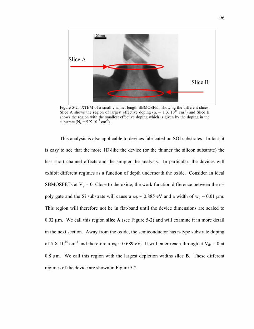
96
Slice B
Slice A
Figure 5-2. XTEM of a small channel length SBMOSFET showing the different slices. Slice A shows the region of largest effective doping (ns ~ 1 X 1019 cm-3) and Slice B shows the region with the smallest effective doping which is given by the doping in the substrate (Nd = 5 X 1015 cm-3).
This analysis is also applicable to devices fabricated on SOI substrates. In fact, it
is easy to see that the more 1D-like the device (or the thinner the silicon substrate) the
less short channel effects and the simpler the analysis. In particular, the devices will
exhibit different regimes as a function of depth underneath the oxide. Consider an ideal
SBMOSFETs at Vg = 0. Close to the oxide, the work function difference between the n+
poly gate and the Si substrate will cause a ψb ~ 0.885 eV and a width of wd ~ 0.01 µm.
This region will therefore not be in flat-band until the device dimensions are scaled to
0.02 µm. We call this region slice A (see Figure 5-2) and will examine it in more detail
in the next section. Away from the oxide, the semiconductor has n-type substrate doping
of 5 X 1015 cm-3 and therefore a ψb ~ 0.689 eV. It will enter reach-through at Vds = 0 at
0.8 µm. We call this region with the largest depletion widths slice B. These different
regimes of the device are shown in Figure 5-2.

97
5.2. Comparison with Experiments
We first consider different size devices on A wafer at room temperature. Figure 5-3
show the experimental change in device characteristics as the length is made smaller.
Figure 5-3a shows the device at a small Vds value and 5-3b at a value for which the
device would operate. The 1.67 µm channel device shows an increased on/off ratio at the
higher Vds value. This is the expected behavior as an increase in Vds should result in an
increase in the drive current, while maintaining the leakage current at a small value. On
the other hand, the smaller channel length devices show a decrease in the on/off ratio
with the larger |Vds| values.
10-14
10-12
10-10
10-8
10-6
10-4
Cur
rent
(Am
ps/µ
m)
-2.0-1.5-1.0-0.50.0Gate Voltage (V)
Channel length = 1.67 µm 0.7 µm 0.3 µm 0.05 µm
a)

98
10-14
10-12
10-10
10-8
10-6
10-4
Cur
rent
(Am
ps/µ
m)
-2.0-1.5-1.0-0.50.0Gate Voltage (V)
Channel length = 1.67 µm 0.7 µm 0.5 µm 0.05 µm
b)
Figure 5-3. Comparison of Device characteristics for different channel lengths at a) Vds = -0.05 V and b) Vds = -1.0 V. Note that only the largest device shows an increase in the on/off ratio in b), indicating that the device suffers from short channel effects which worsen as the dimensions are made smaller.
We expand the ‘slice’ analysis in the above section to devices of different sizes.
From equations (5.1) and (5.2), it is seen that decreasing the gate length causes VRT and
VFB to decrease. We calculate these values for the various experimental devices and the
results are shown in Table 5-1. Based on slice A, we see that none of the devices should
exhibit short channel effects. This means that the intrinsic scaling properties of these
devices are very advantageous as compared to traditional MOSFETs. Given the
experimental data in Figure 5-3, we can conclude that the short channel effects in these
devices are caused by a sub-surface reach-through due primarily to Slice B.
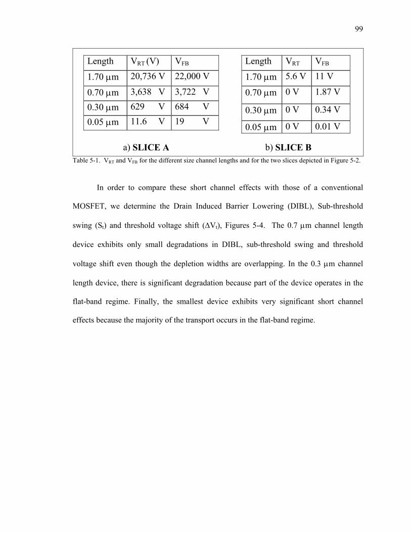
99
Length VRT (V) VFB
1.70 µm 20,736 V 22,000 V
0.70 µm 3,638 V 3,722 V
0.30 µm 629 V 684 V
0.05 µm 11.6 V 19 V
Length VRT VFB
1.70 µm 5.6 V 11 V
0.70 µm 0 V 1.87 V
0.30 µm 0 V 0.34 V
0.05 µm 0 V 0.01 V a) SLICE A b) SLICE B
Table 5-1. VRT and VFB for the different size channel lengths and for the two slices depicted in Figure 5-2.
In order to compare these short channel effects with those of a conventional
MOSFET, we determine the Drain Induced Barrier Lowering (DIBL), Sub-threshold
swing (St) and threshold voltage shift (∆Vt), Figures 5-4. The 0.7 µm channel length
device exhibits only small degradations in DIBL, sub-threshold swing and threshold
voltage shift even though the depletion widths are overlapping. In the 0.3 µm channel
length device, there is significant degradation because part of the device operates in the
flat-band regime. Finally, the smallest device exhibits very significant short channel
effects because the majority of the transport occurs in the flat-band regime.

100
60
50
40
30
20
10
0
DIB
L (∆
Vg/∆
Vds in m
V/V
)
1 .61 .41 .21 .00 .80 .60 .4L ength (µ m)
220
200
180
160
140
120
100
80
S t(mV
/dec
ade)
D IBL Subthresho ld Swing
a)
-0.90
-0.85
-0.80
-0.75
-0.70
Thre
shol
d V
olta
ge (V
)
1 .61.41.21.00.80.60.40.2
Length (µ m) b)
Figure 5-4. Conventional MOSFET scaling parameters for devices on the A wafer.
We have shown that in a well-behaved SBMOSFET, the smallest leakage current
should occur at L ~ Ws + Wd, and that device operation in the flatband regime should be
avoided. The values for slice A agree well with the feasibility predictions of sub-50 nm
devices that have been made from more complex models (Tucker 1995) and experimental
research (Saitoh 1999; Kedzierski 2000a). In particular, we see that scaling is limited not
101
by fundamental considerations of device structure, but by process feasibility in using
either an ultra-thin SOI substrate, well-designed reach-through stoppers or highly tapered
contacts.
Chapter 6
Low Temperature Characteristics
We now investigate the low temperature properties of SBMOSFETs in greater detail.
First, we extend the discussion of the different transport regimes introduced in Section
4.3. In section 6.1 we discuss the transition from thermionic field to field emission. In
Section 6.2, the direct tunneling equation developed in Section 2.2.B is used to
investigate the device properties at low temperatures and in particular the effective
masses of the different valence bands are obtained. We observe oscillations about the
direct tunneling fit, and we investigate the influence of impurities located near the
metal/semiconductor interface. Section 6.3 shows how such impurities can modify the
potential at the barrier and Section 6.4 explores the possible origins of the impurities. In
Section 6.5 we discuss the transport through such localized states, and it is shown that a
simple Lorentzian cannot account for the observed transport.
There are two types of measurements that might be performed on a system with a
localized state that exhibits resonant tunneling behavior. The first is to measure the
current as |Vds| is swept. In this case, the current exhibits a step because the localized
state is shifted up with bias. Out of resonance, the current will either drop back to zero if
103
the tunneling current is very small or continue increasing if it is large. These types of
measurements were used to examine localized states in RTDs (Deshpande 1998). The
other measurement is to sweep the gate voltage and measure the current, or effectively
the conductance. The gate voltage changes the Fermi level of the 2DEG and as it is
swept through the resonant state, the conductance should exhibit a Lorentzian or Breit-
Wigner (BW) peak if there is no quantum interference. We concentrate here only on the
Id-Vg characteristics.
6.1. Thermionic Field vs. Field Emission
We first consider the transport limits discussed in Section 4.3, but at lower temperatures.
Figure 6-1 shows the limits at 185 K obtained using equations (4.4) and (4.5). As
compared to the room temperature limits (Figure 4-5), the field emission regime takes up
a smaller portion of the Vg range because of the reduced carrier concentration at the
surface. The thermionic emission regime has also been reduced because of the
exponential dependence on temperature (Equation 4.8). There is thus a larger thermionic
field emission regime.
The expression for the thermionic field equation as a function of gate bias is in
general much more complicated than the field emission equation (see Appendix B).
Using the guidelines provided from the current transport limits in Figure 6-1; however,
we can qualitatively distinguish these regimes. In Figure 6-2 we plot the Is vs Vg at 190
K for several values of Vds bias. As compared to Figure 1-2b, there are clearly two
regimes visible in the ‘on’ state. In the Vds = -0.05 V curve, the characteristic is very
similar to that in Figure 1-2b. However, the on/off ratio determined by the effective
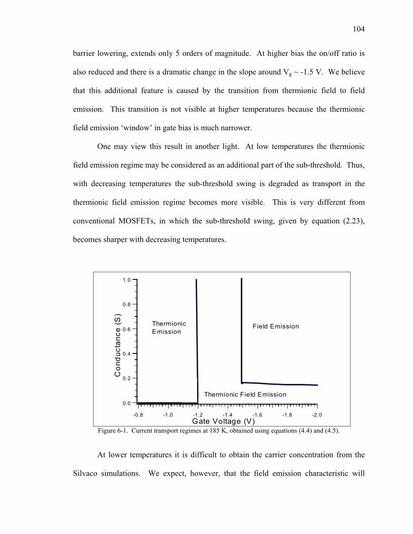
104
barrier lowering, extends only 5 orders of magnitude. At higher bias the on/off ratio is
also reduced and there is a dramatic change in the slope around Vg ~ -1.5 V. We believe
that this additional feature is caused by the transition from thermionic field to field
emission. This transition is not visible at higher temperatures because the thermionic
field emission ‘window’ in gate bias is much narrower.
One may view this result in another light. At low temperatures the thermionic
field emission regime may be considered as an additional part of the sub-threshold. Thus,
with decreasing temperatures the sub-threshold swing is degraded as transport in the
thermionic field emission regime becomes more visible. This is very different from
conventional MOSFETs, in which the sub-threshold swing, given by equation (2.23),
becomes sharper with decreasing temperatures.
1.0
0.8
0.6
0.4
0.2
0.0
Con
duct
ance
(S)
-2.0-1.8-1.6-1.4-1.2-1.0-0.8Gate Voltage (V)
Field Emission
Thermionic Field Emission
Thermionic Emission
Figure 6-1. Current transport regimes at 185 K, obtained using equations (4.4) and (4.5).
At lower temperatures it is difficult to obtain the carrier concentration from the
Silvaco simulations. We expect, however, that the field emission characteristic will

105
become more important as all of the thermal assisted processes are reduced. This is
clearly visible in Figure 6-3. In particular, the characteristics at temperatures below 100
K are dominated by field emission.
10-13
10-12
10-11
10-10
10-9
10-8
10-7
10-6
10-5
10-4
Cur
rent
(Am
ps)
-2.0-1.8-1.6-1.4-1.2-1.0-0.8-0.6Gate Voltage (V)
Vds -0.05 V -0.50 V -1.00 V
190 K
Figure 6-2. Sub-threshold characteristics of the large channel device on A16 at 190 K.
10-12
10-10
10-8
10-6
10-4
Cur
rent
(Am
ps)
-2.0-1.5-1.0-0.50.0Gate Voltage (V)
298 K 240 K 185 K 140 K 80 K
Thermionic Emission Thermionic
FieldEmission
Figure 6-3. Transfer characteristics at different temperatures in large channel device on A16. The Vds bias is –0.5 mV.

106
6.2. Field Emission at Low Temperatures
We now investigate the transport at cryogenic temperatures using the direct tunneling
equation (2.18) to fit the current as a function of Vg. To highlight the important
dependence of this equation we rewrite it in the following form:
21
** exp b
g t
K mJ K V m NV V
φ = − −
(6.1)
where K1 and K2 are constants. Note that in large channel SBMOSFETs part of the
voltage is dropped both at the barrier and in the channel and thus the voltage V across the
junction is not necessarily equal to Vds. From the analysis of the direct tunneling in
Chapter 2, we expect that for Vds << φb the bias will be dropped equally at the forward
and reverse biased Schottky barriers.
The error introduced by using this equation instead of the more exact one
obtained using parabolic transmission coefficients, equation (B.5), is caused by a pre-
exponential logarithm that is constant with carrier concentration. For Vds = -5 mV, this
implies that equation (6.1) underestimates the current by about 10%. For this reason and
because the relevant dependence on the pre-exponential is very weak, we obtain the
effective mass by examining only the exponential dependence. We note that the values
obtained for the pre-exponential are of the correct order of magnitude. This equation was
derived with the assumption that the dispersion of the semiconductor is parabolic;
however, it is well known that valence bands may be highly non-parabolic. As a result,
the characteristics may not exactly follow the shape predicted by equation (6.1).

107
In Figure 6-4, we plot the current as a function of 1g tV V−
, (a), and gate bias,
(b), for device FQ2 at 77 K and 4.2 K. The SBMOSFET has a width / length = 10 µm /
0.7 µm and is a p-type accumulation layer, unlike the p-type inversion layers we
discussed previously. Only the 4.2 K data is fit to equation (6.1) because the 77 K curve
cannot be approximated using this low temperature form. Three linear regions are visible
in Figure 6-4a, each of which corresponds to a different effective mass. We expect the
first mass to be a heavy hole with mhh* ~ 0.49, the next mass to be due to the light hole
mlh* ~ 0.2, and the third mass, the first excited state of the light hole, to be mhhe* ~ 0.2.
The fits work quite well, yielding mhh* = 0.55, mlh* = 0.27 and mhhe* = 0.18. The
effective masses of hole-type layers in silicon can change dramatically on the orientation
of the channel and are found to be dependent on gate voltage (Ando 1984; von Klitzing
1974a; von Klitzing 1974b). In addition, researchers have found a variety of different
effective masses in conventional MOSFETs and the values obtained here are well within
the reported variation (Ando 1984). Finally, we note that around the fits, the current
oscillates in three places: at Vg = -1.55 V, -1.89 V and –1.94 V.
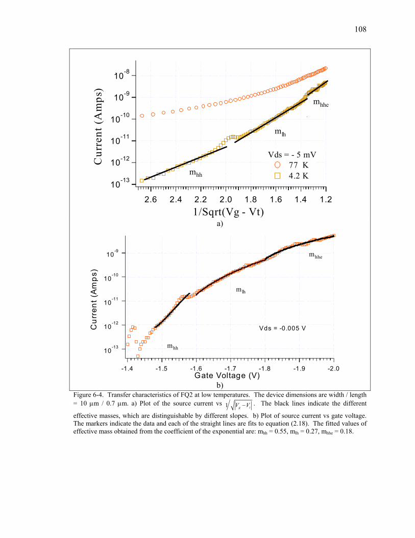
108
10-13
10-12
10-11
10-10
10-9
10-8
Cur
rent
(A
mps
)
2.6 2.4 2.2 2.0 1.8 1.6 1.4 1.21/Sqrt(Vg - Vt)
Vds = - 5 mV 77 K 4.2 Kmhh
mlh
mhhe
a)
10-13
10-12
10-11
10-10
10-9
Cur
rent
(A
mps
)
-2.0-1.9-1.8-1.7-1.6-1.5-1.4Gate Voltage (V)
mhh
mlh
mhhe
Vds = -0.005 V
b)
Figure 6-4. Transfer characteristics of FQ2 at low temperatures. The device dimensions are width / length = 10 µm / 0.7 µm. a) Plot of the source current vs 1 g tV V− . The black lines indicate the different
effective masses, which are distinguishable by different slopes. b) Plot of source current vs gate voltage. The markers indicate the data and each of the straight lines are fits to equation (2.18). The fitted values of effective mass obtained from the coefficient of the exponential are: mhh = 0.55, mlh = 0.27, mhhe = 0.18.
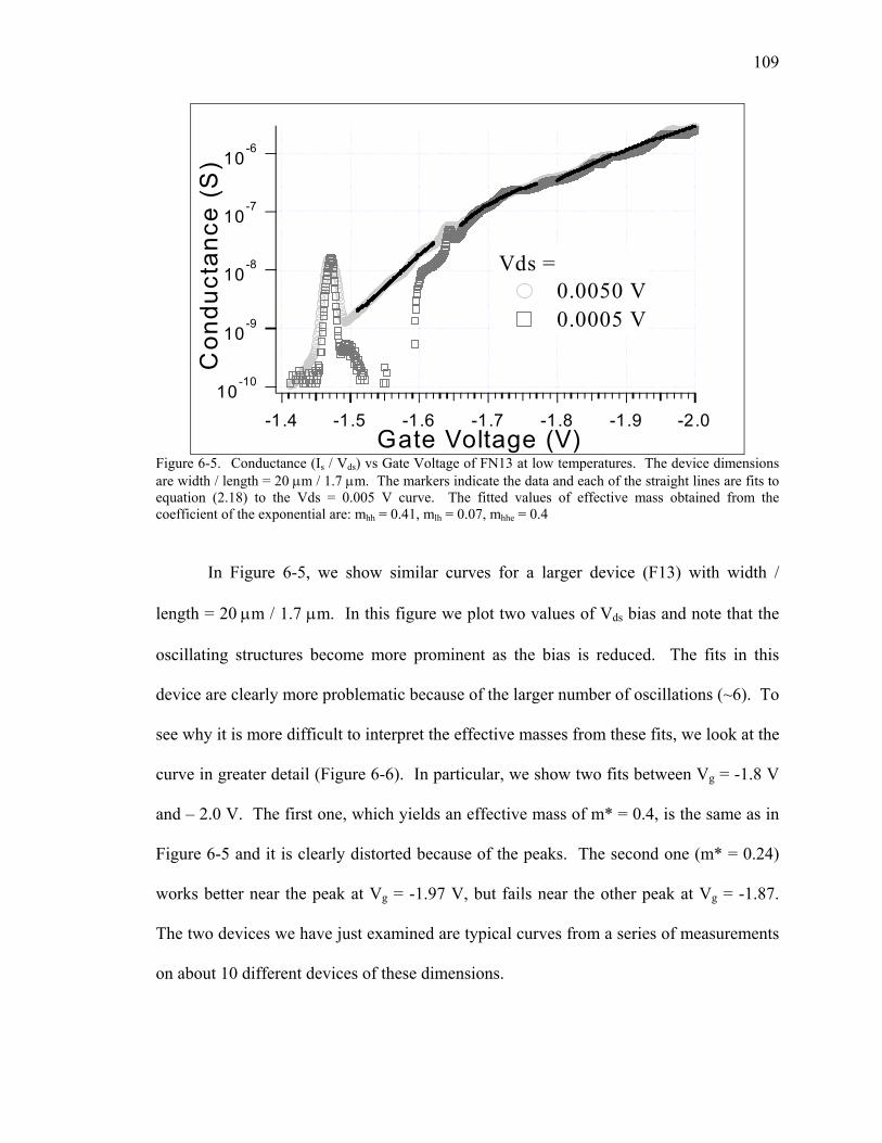
109
10-10
10-9
10-8
10-7
10-6
Con
duct
ance
(S
)
-2.0-1.9-1.8-1.7-1.6-1.5-1.4Gate Voltage (V)
Vds = 0.0050 V 0.0005 V
Figure 6-5. Conductance (Is / Vds) vs Gate Voltage of FN13 at low temperatures. The device dimensions are width / length = 20 µm / 1.7 µm. The markers indicate the data and each of the straight lines are fits to equation (2.18) to the Vds = 0.005 V curve. The fitted values of effective mass obtained from the coefficient of the exponential are: mhh = 0.41, mlh = 0.07, mhhe = 0.4
In Figure 6-5, we show similar curves for a larger device (F13) with width /
length = 20 µm / 1.7 µm. In this figure we plot two values of Vds bias and note that the
oscillating structures become more prominent as the bias is reduced. The fits in this
device are clearly more problematic because of the larger number of oscillations (~6). To
see why it is more difficult to interpret the effective masses from these fits, we look at the
curve in greater detail (Figure 6-6). In particular, we show two fits between Vg = -1.8 V
and – 2.0 V. The first one, which yields an effective mass of m* = 0.4, is the same as in
Figure 6-5 and it is clearly distorted because of the peaks. The second one (m* = 0.24)
works better near the peak at Vg = -1.97 V, but fails near the other peak at Vg = -1.87.
The two devices we have just examined are typical curves from a series of measurements
on about 10 different devices of these dimensions.

110
10-7
2
3
4
5
678
10-6
2
3
4
5
Con
duct
ance
(S)
-2.00-1.95-1.90-1.85-1.80-1.75Gate Voltage (V)
Vds = 5 mV Data Fit 1 Fit 2
Figure 6-6. Two different fits for the device in Figure 6-4. Fit 1 is the same as in Figure 6-4, Fit 2, is performed trying to capture the linearity around the resonance feature between Vg = -1.95 V and –2.0 V.
6.3. Effect of an Impurity Potential on a Schottky Barrier
From previous research on the effect of impurities in nanostructures (Dellow 1992;
Deshpande 1996; Kopley 1989), we expect that the random peaks in Figure 6-5 and 6-6
are caused by impurities. In the conduction band, the metal induces negative charge at
the metal/semiconductor interface, which is balanced by positively charged donors in an
n-type semiconductor. The barrier height is on average a constant value throughout the
contact; however, on a microscopic level, the random placement of donor impurities near
the barrier will give rise to local fluctuations. In particular, some localized states are
situated closer to the barrier than others and will result in a smaller barrier height than the
bulk average. To see this effect, we simulate the total potential formed by adding
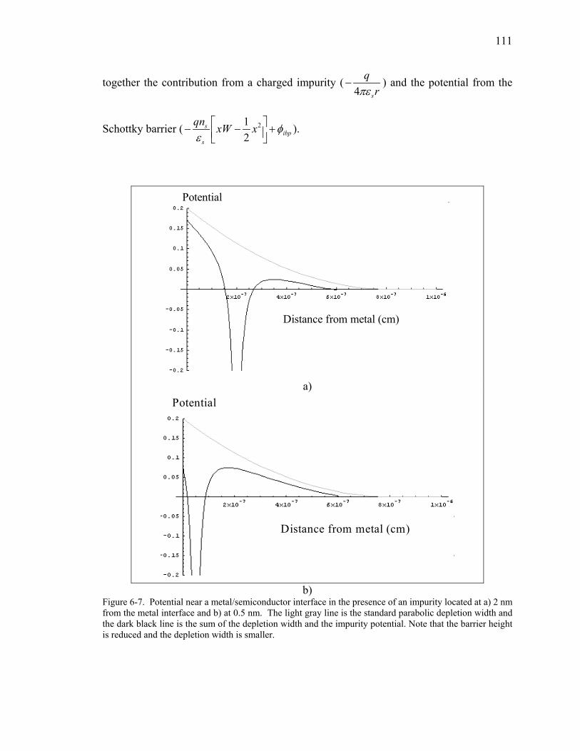
111
together the contribution from a charged impurity (4 s
qrπε
− ) and the potential from the
Schottky barrier ( 212
sibp
s
qn xW x φε
− − + ).
Distance from metal (cm)
Potential
a)
Distance from metal (cm)
Potential
b)
Figure 6-7. Potential near a metal/semiconductor interface in the presence of an impurity located at a) 2 nm from the metal interface and b) at 0.5 nm. The light gray line is the standard parabolic depletion width and the dark black line is the sum of the depletion width and the impurity potential. Note that the barrier height is reduced and the depletion width is smaller.

112
Figure 6-7 demonstrates that the closer the impurity is situated to interface, the greater
the barrier height reduction. In this analysis we have assumed the presence of donors in a
conduction band, but that it also holds for acceptors in a valence band in a degenerate
accumulation layer. In particular, to simulate the parameters of a valence band, we could
invert the y-axis. The parameters used in the simulations are valid parameters from the
SBMOSFET system at 4K: Ns = 4 X 1018 cm-3, W = 8 nm, φibp = 0.2 eV.
Viewed in three dimensions (Figure 6-8), the resultant ‘tracks’ in the depletion
width give rise to regions of enhanced tunneling where the barrier height is reduced. At
low temperatures, a charged impurity will thus have two important effects on the
potential: it gives rise to discrete states caused by quantum confinement and it enhances
the probability of tunneling nearby because of the reduction in barrier height.
Figure 6-8. 3D plot of the potential towards the channel (x) and physical width (y) of the device. There are two impurities in this plot, one located at (4 nm, 0.1 µm) and the other at (2 nm, 0.3 µm).
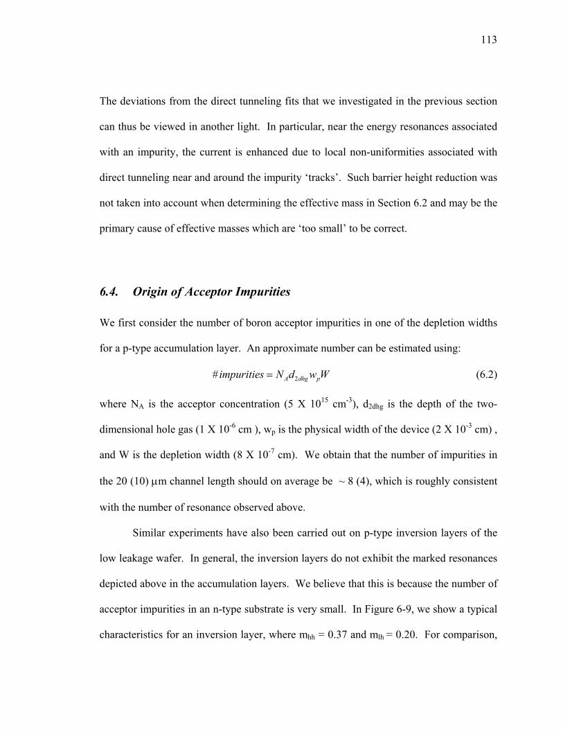
113
The deviations from the direct tunneling fits that we investigated in the previous section
can thus be viewed in another light. In particular, near the energy resonances associated
with an impurity, the current is enhanced due to local non-uniformities associated with
direct tunneling near and around the impurity ‘tracks’. Such barrier height reduction was
not taken into account when determining the effective mass in Section 6.2 and may be the
primary cause of effective masses which are ‘too small’ to be correct.
6.4. Origin of Acceptor Impurities
We first consider the number of boron acceptor impurities in one of the depletion widths
for a p-type accumulation layer. An approximate number can be estimated using:
2# A dhg pimpurities N d w W= (6.2)
where NA is the acceptor concentration (5 X 1015 cm-3), d2dhg is the depth of the two-
dimensional hole gas (1 X 10⁻⁶ cm ), wp is the physical width of the device (2 X 10⁻³ cm) ,
and W is the depletion width (8 X 10⁻⁷ cm). We obtain that the number of impurities in
the 20 (10) µm channel length should on average be ~ 8 (4), which is roughly consistent
with the number of resonance observed above.
Similar experiments have also been carried out on p-type inversion layers of the
low leakage wafer. In general, the inversion layers do not exhibit the marked resonances
depicted above in the accumulation layers. We believe that this is because the number of
acceptor impurities in an n-type substrate is very small. In Figure 6-9, we show a typical
characteristics for an inversion layer, where mhh = 0.37 and mlh = 0.20. For comparison,

114
we have included in this graph, the –0.1 mV sweep as well. This characteristic does
exhibit some small oscillatory structure, which may be due to the deep level acceptor
states of Pt.* In particular, during processing Pt diffuses into the Si substrate and when
the ratio of Pt:Si is 1:1, PtSi can form. However, close to the interface, the amount of Pt
can be slightly less than the concentration of Si atoms so that there is not a silicide but
still a large concentration of Pt dopants. The resonances are smaller in magnitude than in
the accumulation layers, which may be caused by the position of the acceptor level (0.34
above the valence band).
10-9
2
4
6
10-8
2
4
610
-7
2
Con
duct
ance
(S)
-2.0-1.9-1.8-1.7-1.6Gate Voltage (V)
Vds = -0.5 mV -0.1 mV
Figure 6-9. Transfer characteristics of a p-type inversion layer (device A43) at 4.2 K, width / length = 20 µm / 2 µm. Note that there are not the large oscillations exhibited in Figures 6-2 and 6-3. The dark solid lines are fits are carried out on the Vds = -0.5 mV curve (markers). Also shown in a light solid line is a Vds = -0.1 mV curve, indicating that there are some oscillations at low bias.
* In the next chapter we will see that one signature of the Fano resonance in this system is that reversing the bias transforms peaks into dips and vice versa. This effect is also observed in the p-type inversion layers, but because the resonances are so weak, fitting to the Fano form is very difficult.
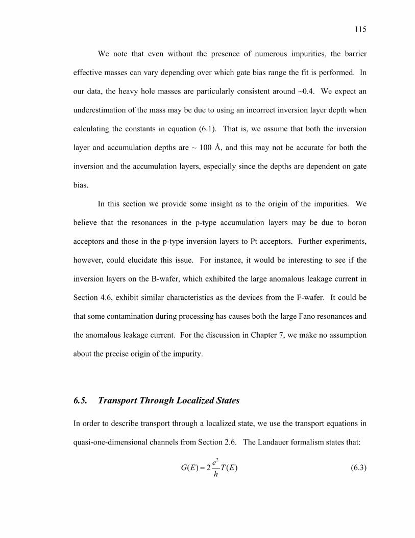
115
We note that even without the presence of numerous impurities, the barrier
effective masses can vary depending over which gate bias range the fit is performed. In
our data, the heavy hole masses are particularly consistent around ~0.4. We expect an
underestimation of the mass may be due to using an incorrect inversion layer depth when
calculating the constants in equation (6.1). That is, we assume that both the inversion
layer and accumulation depths are ~ 100 Å, and this may not be accurate for both the
inversion and the accumulation layers, especially since the depths are dependent on gate
bias.
In this section we provide some insight as to the origin of the impurities. We
believe that the resonances in the p-type accumulation layers may be due to boron
acceptors and those in the p-type inversion layers to Pt acceptors. Further experiments,
however, could elucidate this issue. For instance, it would be interesting to see if the
inversion layers on the B-wafer, which exhibited the large anomalous leakage current in
Section 4.6, exhibit similar characteristics as the devices from the F-wafer. It could be
that some contamination during processing has causes both the large Fano resonances and
the anomalous leakage current. For the discussion in Chapter 7, we make no assumption
about the precise origin of the impurity.
6.5. Transport Through Localized States
In order to describe transport through a localized state, we use the transport equations in
quasi-one-dimensional channels from Section 2.6. The Landauer formalism states that:
2
( ) 2 ( )eG E T Eh
= (6.3)

116
Assuming that the transport is incoherent in the quasi-1D channel where the localized
state is, we can incorporate the effect of the direct tunneling component discussed earlier
in this section by adding equations (6.1) and (6.3).
Equation (6.3) strictly applies to measurements performed in the linear transport
regime, which means that the transmission coefficient is, to first order, independent of the
applied bias, Vbias. Since we will be interested in the change in the conductance with Vds
bias that is larger than kT, we must first make sure that we are in the linear regime.
Normally, the condition that the response is linear is that Vds << kBT (Datta, page 89);
however, since the bias is not just dropped where the quasi 1D channel is, this condition
is may not apply to the SBMOSFETs considered here. The simplest way to determine if
we are in fact in the linear regime is to see how the conductance changes for different Vds
bias. If transport is linear, the curves should have approximately the same conductance
for different Vds bias. If not then T(E) and thus G will increase with bias. This analysis,
however, is complicated because the 3D tunneling current is also linear for small bias
(see equation (6.1). It may be that transport through the discrete state is not linear (Vds >
kT/q), but the transport through the large barrier width is (Vds << φb) and thus care must
be taken when investigating Vds > kT/q.
Model of Impurity State
We assume that the impurities are shallow acceptors, and thus that a hydrogenic model
can be employed. In this case, the energy levels are:

117
4
02 4h
n
s
m eEhπε ε
=( )
2
02 2 2
0
1 113.6 h
s
m eVn m n
εε
=
and the Bohr radius is:
2
0 * 2sh
hrm e
ε επ
= .
If we assume the heavy hole (light hole) mass of 0.49 m0 (0.16 m0) then E0 ~ 46 meV (15
meV) and r ~ 1.3 nm (4.0 nm). (Ibach, pg.284). Empirically, the acceptor properties of
impurities in silicon have been examined in bulk samples either by measuring the change
in the conducting carriers as a function of temperature or by photo-absorption in which
one observes the photon energy necessary to raise a carrier from the ground to excited
state. (For an excellent review see, Kohn 1957). Both of these methods examined
impurities in bulk samples and not a single impurity state. The energy levels of localized
states in confined potentials are found to slightly different from the energy levels given
by this model (Deshpande 1998). In SBMOSFETs, the resonant energy of an impurity
depends on its position relative to other impurities and the metal/semiconductor interface.
This agrees with the experimental result that the position of the resonances with respect
to gate voltage varies from device to device.
We can determine the movement of the Fermi level with respect to gate bias. In
particular, the 2DHG of the MOSFET has a density of states given by:
37 1 22
2 *( ) 2.84 10hhhh
mD E X J mhπ
− −= =/
(6.4)
( Dlh(E) = 9.30 X 1036 ) where m* = mhh = 0.49 and mlh = 0.16 and a degeneracy of 2
has been assumed. The capacitance/unit area is: C/A = εs/dox = 1.01 x 10⁻² F/m2. The
number of electrons/area is thus:

118
( )surf g t facc
Cn V V D E EqAd
= − = (6.5)
We thus find that the gate voltage to Fermi energy conversion α is:
1 ~ 14 /( )
f oxhh
g hh
dE C meV VdV eA D E
α = = (6.6)
and 42.5 meV/V for light holes. While in the heavy hole band, the small α implies that
the Fermi level is moved only ~ 0.007 eV below the bottom of the valence band in the Vg
range considered here, in the light hole band the gate bias moves the Fermi level even
further.
Transmission Coefficient
The simplest form for the transmission coefficient T(E) is the Lorentzian lineshape,
described in Section 2.6 (Equation (2.27)). This predicts that on resonance (E = E0) there
will be an enhancement of the conductance. If the barriers are equal (ΓL = ΓR), and the
temperature is low enough so that there is no broadening; the conductance is expected to
reach a peak of 2e2/h. If the barriers are unequal (ΓL << ΓR) and/or if there is temperature
broadening, then the conductance peak can be substantially lower than 2e2/h.
In the SBMOSFET measurements, we observe structures that cannot be described
by this simple formalism. As shown in Figure 6-10 and Figure 6-11, we find that the
transfer characteristics can exhibit resonant peaks and resonant dips.
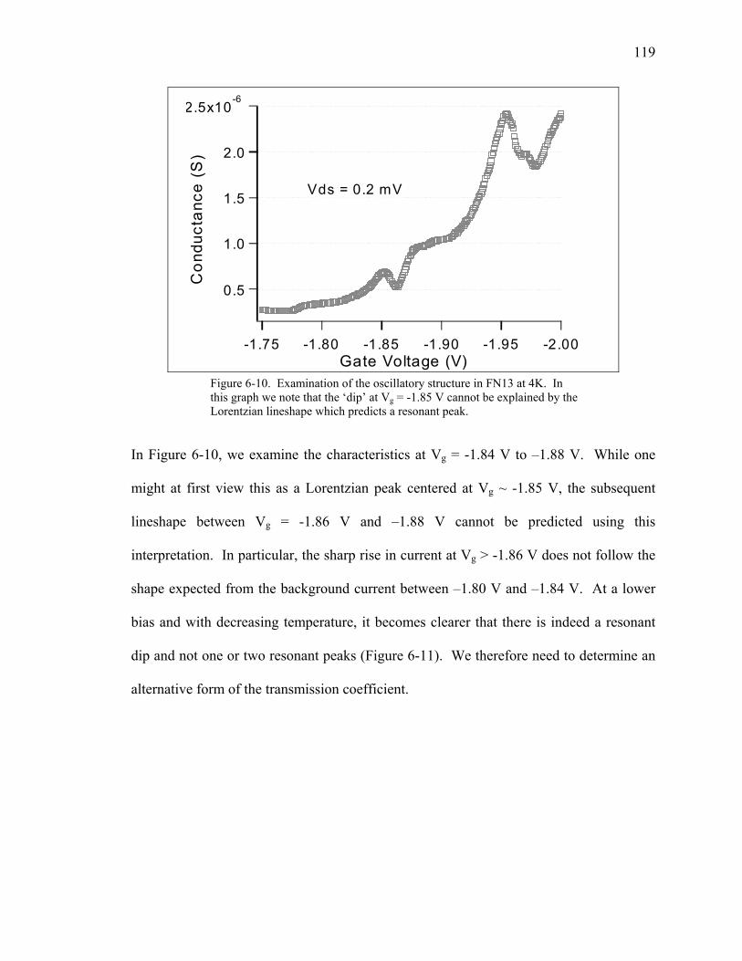
119
2.5x10⁻⁶
2.0
1.5
1.0
0.5
Con
duct
ance
(S
)
-2.00-1.95-1.90-1.85-1.80-1.75Gate Voltage (V)
Vds = 0.2 mV
Figure 6-10. Examination of the oscillatory structure in FN13 at 4K. In this graph we note that the ‘dip’ at Vg = -1.85 V cannot be explained by the Lorentzian lineshape which predicts a resonant peak.
In Figure 6-10, we examine the characteristics at Vg = -1.84 V to –1.88 V. While one
might at first view this as a Lorentzian peak centered at Vg ~ -1.85 V, the subsequent
lineshape between Vg = -1.86 V and –1.88 V cannot be predicted using this
interpretation. In particular, the sharp rise in current at Vg > -1.86 V does not follow the
shape expected from the background current between –1.80 V and –1.84 V. At a lower
bias and with decreasing temperature, it becomes clearer that there is indeed a resonant
dip and not one or two resonant peaks (Figure 6-11). We therefore need to determine an
alternative form of the transmission coefficient.
120
-80x10-12
-60
-40
-20
0
Cur
rent
(A
mps
)
-1.90-1.88-1.86-1.84-1.82-1.80Gate Voltage (V)
Temperature 5.0 K 3.7 K
Figure 6-11. Example of transport characteristics that cannot be described by the Lorentzian lineshape. Vds = -0.1 mV.
One possibility as to why the Lorentzian does not work in this system is that the
impurity both gives rise to both resonant tunneling and enhanced direct tunneling. If
there is coherence between the localized state and some portion of the direct tunneling,
then we need to incorporate this directly into the transmission coefficient T(E). To
maintain phase coherence across the Schottky barrier, the width of the barrier must be
smaller than or approximately equal to the Fermi wavelength 2f
snπλ = (Datta 1995).
We study the impurity in Figure 6-8 and 6-9 in greater detail in Chapter 7 and so we
determine the Fermi wavelength at this value of Vg. In particular, it is centered at ~-
1.86V and turn on is approximately at –1.25 V. Using equation (6.5), we obtain ns = 4 X
1012 cm-2 and thus a Fermi wavelength of wavelength λf = 12.5 nm.
The depletion width of the Schottky barrier can be estimated using equation (2.5).
At low temperatures, ψbi = φb – (Ev – Ef) = 0.155 eV, where (Ev – Ef) = 0.045 eV is the

121
position of the donor level relative to valence band. Using V ~ 0.1 mV and kT/q = 0.320
mV, N = ns εox/(εs tox) = 4 X 1018 cm-3 we estimate that W ~ 8 nm. Note that if an
impurity is located at an edge of the barrier close to the semiconductor it effectively
makes the Schottky Barrier much narrower and results in ‘continuum’ states that are not
bound. Finally, we note that the total depletion width is not affected by very small
changes in Vds, but that if an impurity is situated asymmetrically in the barrier, it can
have a dramatic effect since Vds ~ φibp.
We thus see that the Fermi wavelength is larger than the depletion width and that
phase coherence can be maintained over the length of the Schottky barrier. This result,
along with our preliminary observation that a Lorentzian cannot be used to analyze the
majority of the observed resonant structure, have now set the stage for the quantum
interference analyzed in the next chapter.

Chapter 7
Fano Resonances
We continue the discussion from the previous chapter on the low temperature properties
of SBMOSFETs. We find that the transmission coefficient that can accurately predict the
oscillatory behavior in our devices is the Fano lineshape. This form arises when there is
interference between a discrete state and a continuum. In SBMOSFETs, the continuum
corresponds to direct tunneling through the Schottky Barrier and the discrete state to the
resonance associated with the confined potential of an impurity. The condition for such
interference is that the direct tunneling component be relatively large as compared to the
resonant state. For this to occur, an impurity in the depletion width must be located near
the metal so that the barrier height is dramatically reduced, as in Figure 6-7b.
Fano resonances (Fano 1961) were first introduced to describe interference
between a discrete auto-ionized state and a continuous configuration spectrum and have
since been found to be a general phenomenon. In addition to resonant scattering in atoms
(see Schulz 1973 for a review); such resonances have been observed in photoionization,
electron and neutron scattering, Raman scattering, and photoabsorbtion in quantum well
structures. Observation in electrical transport has been more elusive. An early report of
resonant tunneling in a split gate technique was suggestive of Fano resonances (McEuen
123
1991). More resonantly Gores (2000) observed the phenomenon in a SET; however in
this case the interference involved a Coulomb Blockaded state and there were several
paths onto the dot.
SBMOSFETs are uniquely suited to examining Fano resonances because the
interference exists without electron-electron interactions, which have previously
complicated interpretations in other mesoscopic systems. Nearly every long channel/long
width accumulation layer device exhibits this behavior at relatively high (1.5 –15 K)
cryogenic temperatures. In addition, we often find impurities that are relatively stable
after thermal cycling so that one device can be studied in detail.
7.1. Theory of Fano Resonances
Solid state theorists have shown that the Fano form is directly applicable in solid state
systems when an interference between a continuum and a discrete state may occur
(Nöckel 1994; Porod 1992; Tekman 1993 and others). The Fano transmission coefficient
can be simply derived by squaring the sum of the probability of direct tunneling and the
probability of resonant tunneling. The result gives rise to a family of lineshapes and can
be written as:
( )2
0 2 1q
T E Tεε
+=
+ (7.1)
where ( )2 resE Eε = − Γ is the reduced energy near the energy resonance Eres, Γ is the
full width at half maximum of the resonant state, T0 is the transmission coefficient for
direct tunneling and q is the asymmetry parameter. The series of lineshapes are
determined by q, which is effectively the ratio between the resonant transition probability

124
and the direct tunneling transition probability. A typical family of such curves is
illustrated in Figure 7-1. We note that q can be positive or negative and that reversing the
sign of q reverses the energy axis in Figure 7-1.
1.0
0.8
0.6
0.4
0.2
0.0
Line
shap
e
-1.0 -0.5 0.0 0.5 1.0Energy (E)
q = 0 q = -1 q = -2 q = -10
Figure 7-1. Family of Fano lineshapes satisfying equation (7.1) with Eres = 0 and Γ = 0.1. Note that the q = 0 and q = -1 curves are scaled by 0.5 and the q = -10 curve is scaled by 1 X 10⁻⁴. The q = -10 curve needs a larger scaling factor because of its large value.
To obtain an intuition for the interference that occurs in the Fano effect, consider
an analogy with the double slit experiment, Figure 7-2. Recall that sunlight falling on a
pinhole creates a spherical wave which when passed through the double slits causes an
interference pattern on a screen at a distance x. In a SBMOSFET, the two paths (resonant
tunneling (A) and direct tunneling(B)) of an electron are like the double slits. Sweeping
the gate bias effectively changes the phase of one of the paths (A) by 180° and thus a
minimum and maximum occur, very much like in this classic optics experiment. Because
the phase of the ‘direct tunneling slit’ (B) can be at a relative phase difference from the
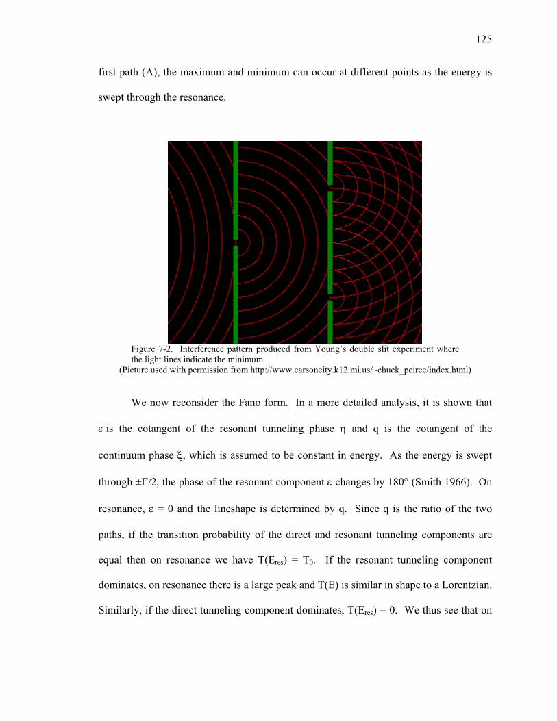
125
first path (A), the maximum and minimum can occur at different points as the energy is
swept through the resonance.
Figure 7-2. Interference pattern produced from Young’s double slit experiment where the light lines indicate the minimum.
(Picture used with permission from http://www.carsoncity.k12.mi.us/~chuck_peirce/index.html)
We now reconsider the Fano form. In a more detailed analysis, it is shown that
ε is the cotangent of the resonant tunneling phase η and q is the cotangent of the
continuum phase ξ, which is assumed to be constant in energy. As the energy is swept
through ±Γ/2, the phase of the resonant component ε changes by 180° (Smith 1966). On
resonance, ε = 0 and the lineshape is determined by q. Since q is the ratio of the two
paths, if the transition probability of the direct and resonant tunneling components are
equal then on resonance we have T(Eres) = T0. If the resonant tunneling component
dominates, on resonance there is a large peak and T(E) is similar in shape to a Lorentzian.
Similarly, if the direct tunneling component dominates, T(Eres) = 0. We thus see that on
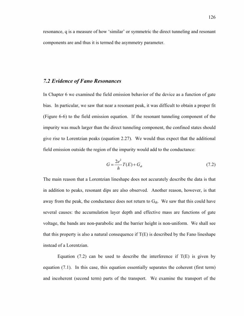
126
resonance, q is a measure of how ‘similar’ or symmetric the direct tunneling and resonant
components are and thus it is termed the asymmetry parameter.
7.2 Evidence of Fano Resonances
In Chapter 6 we examined the field emission behavior of the device as a function of gate
bias. In particular, we saw that near a resonant peak, it was difficult to obtain a proper fit
(Figure 6-6) to the field emission equation. If the resonant tunneling component of the
impurity was much larger than the direct tunneling component, the confined states should
give rise to Lorentzian peaks (equation 2.27). We would thus expect that the additional
field emission outside the region of the impurity would add to the conductance:
22 ( ) dteG T E Gh
= + (7.2)
The main reason that a Lorentzian lineshape does not accurately describe the data is that
in addition to peaks, resonant dips are also observed. Another reason, however, is that
away from the peak, the conductance does not return to Gdt. We saw that this could have
several causes: the accumulation layer depth and effective mass are functions of gate
voltage, the bands are non-parabolic and the barrier height is non-uniform. We shall see
that this property is also a natural consequence if T(E) is described by the Fano lineshape
instead of a Lorentzian.
Equation (7.2) can be used to describe the interference if T(E) is given by
equation (7.1). In this case, this equation essentially separates the coherent (first term)
and incoherent (second term) parts of the transport. We examine the transport of the
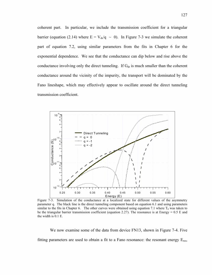
127
coherent part. In particular, we include the transmission coefficient for a triangular
barrier (equation (2.14) where E = Vds/q ~ 0). In Figure 7-3 we simulate the coherent
part of equation 7.2, using similar parameters from the fits in Chapter 6 for the
exponential dependence. We see that the conductance can dip below and rise above the
conductance involving only the direct tunneling. If Gdt is much smaller than the coherent
conductance around the vicinity of the impurity, the transport will be dominated by the
Fano lineshape, which may effectively appear to oscillate around the direct tunneling
transmission coefficient.
10-12
2
4
68
10-11
2
4
6
810
-10
2
4
68
10-9
Con
duct
ance
(S)
0.600.550.500.450.400.350.300.25Energy (E)
Direct Tunneling q = 0 q = -1 q = -2
Figure 7-3. Simulation of the conductance at a localized state for different values of the asymmetry parameter q. The black line is the direct tunneling component based on equation 6.1 and using parameters similar to the fits in Chapter 6. The other curves were obtained using equation 7.1 where T0 was taken to be the triangular barrier transmission coefficient (equation 2.27). The resonance is at Energy = 0.5 E and the width is 0.1 E.
We now examine some of the data from device FN13, shown in Figure 7-4. Five
fitting parameters are used to obtain a fit to a Fano resonance: the resonant energy Eres,
128
the resonant width Γ, the prefactor G0 , the asymmetry parameter, q, and an additive off
resonance term Gextra. In table 7-1, the values of these terms for the fit are shown. Note
that for simplicity, we have assumed that G0 and Gextra are constants. The lineshape we
have examined in Figure 7-4 is located at Vg = -1.86 V. We note that the Lorentzian
lineshape could not accurately account for so much of the resonant structure as the Fano
lineshape. The sudden increase in current at Vg = -1.85 V can be attributed to the rising
importance of the direct tunneling through the impurity as compared to the direct
tunneling through the rest of the channel. Once the gate voltage has swept past the
energy level at Vg = -1.86 V, another impurity structure becomes important at Vg = –1.95
V. In this case, the resonance structure appears to be a peak or a double peak. While at
first sight, it is difficult to disentangle the ‘dips’ and ‘peaks’, as the Vds bias is lowered,
these structures become more pronounced and easier to discern. We now investigate
why, in the same curve, we can see both peaks and dips.
2.5x10⁻⁶
2.0
1.5
1.0
0.5
Con
duct
ance
(S
)
-2.00-1.95-1.90-1.85-1.80Gate Voltage (V)
Vds = 0.0003 V
Figure 7-4. The dashed lines show the experimental data and the solid black lines represent the fit to the Fano form. The conductance was obtained by dividing the current by the Vds value.

129
Vds Value: Eres (V) Γ (V) G0 (µS) q Gextra (µS)
300 µV -1.866 0.021 0.30 -0.39 0.6
Table 7-1. The fitting parameters for the Fano lineshape fits in Figure 7-4.
7.3 Abruptness of the Metal/Semiconductor Interface and Consequences
We consider another analogy from classical physics: the reflection and transmission
between strings of different masses, Figure 7-5. In this classic wave problem, a pulse
traveling down a light string will be reflected 180º out of phase and the reflection will be
greater than the transmission. On the contrary, a pulse traveling down a heavy string will
be mostly transmitted to the light string, and the reflected wave will be in phase with the
transmitted one.
6420
1.0
0.5
0.0
-0.5
-1.0
1.0
0.5
0.0
-0.5
-1.0
6420
0
5
0
5
0
6420
1.0
0.5
0.0
-0.5
-1.0
1.0
0.5
0.0
-0.5
-1.0
a
b
Figure 7-5. Reflections at the interface between heavy and light strings. In analogy with the metal/semiconductor junction, the light string is like the metal and the heavy string the semiconductor.
130
In the metal/semiconductor junction, the metal is equivalent to the light string and
the semiconductor to the heavy string. To see this, we note that
* *k hvm m λ
= = (7.3)
Since the Fermi wavelength of the metal is much smaller (~ 0.5 Å) than that in the
semiconductor (~ 125 Å), the velocity is greater and thus the metal is like the ‘light’
string in the wave analogy. Therefore, most of the carriers incident on the
metal/semiconductor junction from the metal are reflected, and the contrary for carriers
incident on the semiconductor. In a conventional metal/semiconductor junction, such
reflections have been examined and result, for instance, in a reduction of the Richardson
constant in thermionic emission (Crowell 1969). However, the reduction is uniform in
both directions of transport because of the condition that in equilibrium that detailed
balance be satisfied.
While this analogy gives some intuition that transport involving an abrupt
metal/semiconductor interface may complicate the Fano interference, it clearly does not
describe all of the physics. Furthermore, since such reflections do not affect the bias
direction in the case of thermionic emission or direct tunneling, it is not obvious that they
will do so when Fano interference is present. Finally, to truly complete the analogy, in a
SBMOSFET, there is, in some sense, one light string (the metal) and two ‘heavy’
strings—the direct tunneling path and the resonant path. Whether or not reflections will
play a role in determining the transport depends on how they affect the coupling between
these two paths.
131
To see how this relates to Fano interference in SBMOSFETs, we thus need to
reconsider the asymmetry parameter q of the Fano form. In particular, from the original
Fano paper (1961), we write
E
T iq
T iψΦ
∝Γ
(7.4)
where T is the transition operator between an initial state i and a final state, which is
either Eψ , the continuum of states, or Φ , a modified admixture of the discrete state
and the continuum; ϕ is the discrete state and H is the initial Hamiltonian. We are not
concerned with the exact mathematical form of the matrix elements in q, but instead with
the physical interpretation in context of the impurity state.
The direct tunneling transition probability is the square of the matrix containing
the transition between an initial state x and final state y and we thus write:
22E xyT i tψ = . The probability of the electron going from x through the dot to get to
y can be written as: 2 2
2
2 4x d d y
x d
t tT i
tπ→ →
→
= Φ . This formula is arrived at using conditional
probabilities: the probability to go from x to y through the dot is: 2 2x d d yt t
→ →, but it is
conditional on getting to the dot from x: 2x dt → . Putting this together we can rewrite q as:
1 dy
dt
tq
t∝
Γ (7.5)
The asymmetry parameter traveling from either the metal to the semiconductor or the
semiconductor to the dot can thus be written:
1 dsms
ms
tqt
∝Γ
(7.6)

132
1 dmsm
sm
tqt
∝Γ
(7.7)
The condition for quantum interference is an enhancement of the direct tunneling
component near the impurity and thus the impurity must be situated close to the
metal/semiconductor interface so that a reduction in the barrier height results. We
therefore expect that tdm >> tds. At small enough biases, we saw in Chapter 2 that tms ~
tsm. We thus expect that qms << qsm. Figure 7-6 and Table 7-2 illustrate this point for
FN13 at Vds = ± 0.1 mV. We note that we do not know in which barrier the impurity is
located and so the sign of Vds is not important. Contrarily what is important is that
reversing the direction of a very small bias results in a dramatic change in the asymmetry
parameter q. Using this analysis we can thus identify in which contact the barrier is
located. In this case, the impurity is located in the drain barrier because the sign of the
sign of the Vds value is opposite that expected from equations (7.6) and (7.7).
How does this compare with the simple string analogy presented above? The
asymmetry parameter is an indication of ‘how much’ resonant tunneling there is as
compared to the direct tunneling. In other words, the small value of q, which arises when
an electron travels from the metal to the semiconductor, tells us that the ‘resonant
tunneling string’ has less transmission through it than the ‘direct tunneling string’ and
thus appears ‘heavier’. Similarly, when current is transported from the semiconductor to
the metal, qsm is large and thus the ‘resonant tunneling string’ is coupled more strongly
than the ‘direct tunneling string’ and is thus heavier once again. The interference thus
amplifies the effect of transmission through the interface, making a small transmission
even smaller and a large transmission even larger.
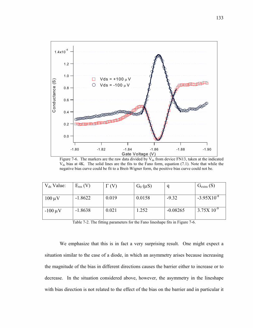
133
1.4x10⁻⁶
1.2
1.0
0.8
0.6
0.4
0.2
0.0
Con
duct
ance
(S)
-1.90-1.88-1.86-1.84-1.82-1.80Gate Voltage (V)
Vds = +100 µ V Vds = -100 µ V
Figure 7-6. The markers are the raw data divided by Vds from device FN13, taken at the indicated Vds bias at 4K. The solid lines are the fits to the Fano form, equation (7.1). Note that while the negative bias curve could be fit to a Breit-Wigner form, the positive bias curve could not be.
Vds Value: Eres (V) Γ (V) G0 (µS) q Gextra (S)
100 µV -1.8622 0.019 0.0158 -9.32 -3.95X10⁻⁸
-100 µV -1.8638 0.021 1.252 -0.08265 3.75X 10⁻⁹
Table 7-2. The fitting parameters for the Fano lineshape fits in Figure 7-6.
We emphasize that this is in fact a very surprising result. One might expect a
situation similar to the case of a diode, in which an asymmetry arises because increasing
the magnitude of the bias in different directions causes the barrier either to increase or to
decrease. In the situation considered above, however, the asymmetry in the lineshape
with bias direction is not related to the effect of the bias on the barrier and in particular it

134
was assumed that the direct tunneling transition probabilities are equal in both directions
(tsm = tms). In fact, in Section 7.5 we shall see that increasing the magnitude of the bias
reduces the asymmetry seen in Figure 7.6. Instead, the asymmetry of the position of the
impurity results in a constructive interference in one bias direction and a destructive
interference in the other.
7.4 Temperature Dependence
In this section we qualitatively examine the result of increasing temperature. To be
strictly correct, the temperature dependence should be accounted for by convolving the
Fermi function with the Fano transmission coefficient. The temperature dependence of
the Fano form is essentially found in the direct tunneling transmission coefficient T0 and
the resonant width Γ. We examine these two parameters independently. An estimation
of the dependence of the direct tunneling transmission coefficient can be obtained by
considering the expression for direct tunneling in Appendix B. In particular, we note that
the temperature dependence of (B.4) is approximately given by 1 + K1T2, obtained by
expanding the T/sin(T) dependence. From equation (2.26), the resonant width can be
approximated by Γ = Γ0 + 3.5 kT.
We rewrite q in a more convenient form to highlight the expected temperature
dependence. We note that 2 2 2 2md ds sd dmt t t tΓ = + = + . In order to have a Fano resonance, we
must have an enhanced probability of tunneling in the channel. In order for this to occur,
the impurity must exist close to the metal/semiconductor interface so that the barrier
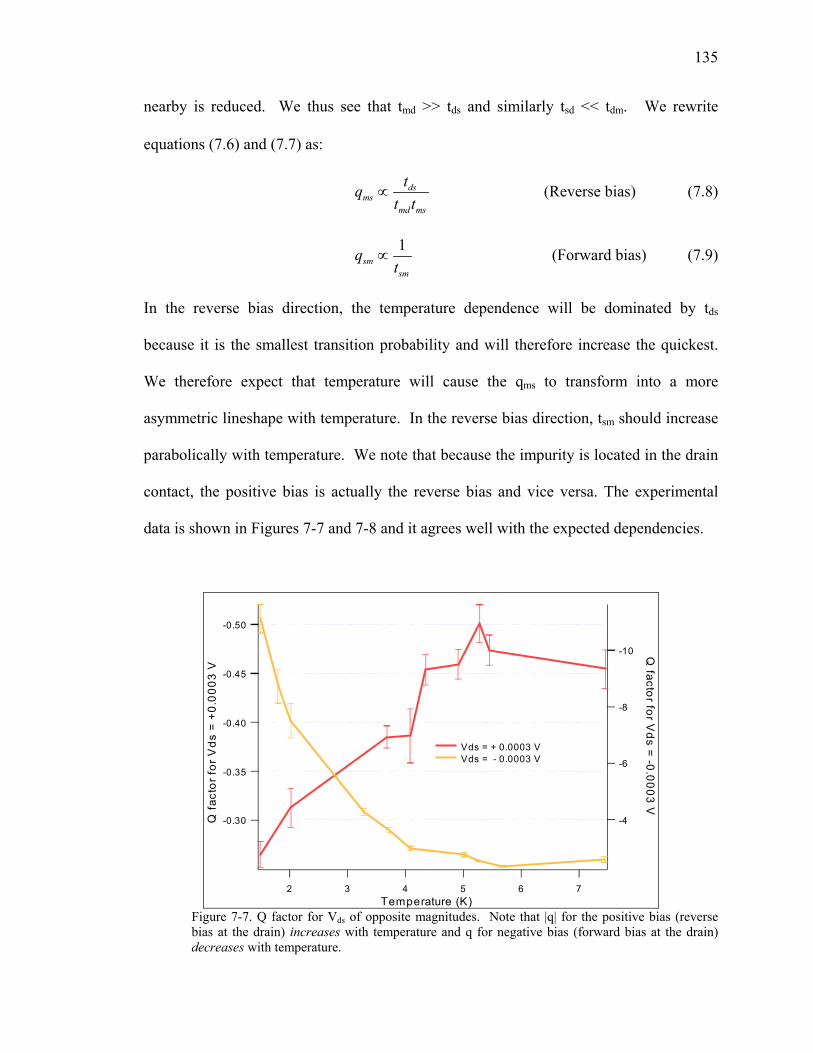
135
nearby is reduced. We thus see that tmd >> tds and similarly tsd << tdm. We rewrite
equations (7.6) and (7.7) as:
dsms
md ms
tqt t
∝ (Reverse bias) (7.8)
1sm
sm
qt
∝ (Forward bias) (7.9)
In the reverse bias direction, the temperature dependence will be dominated by tds
because it is the smallest transition probability and will therefore increase the quickest.
We therefore expect that temperature will cause the qms to transform into a more
asymmetric lineshape with temperature. In the reverse bias direction, tsm should increase
parabolically with temperature. We note that because the impurity is located in the drain
contact, the positive bias is actually the reverse bias and vice versa. The experimental
data is shown in Figures 7-7 and 7-8 and it agrees well with the expected dependencies.
-0.50
-0.45
-0.40
-0.35
-0.30Q fa
ctor
for V
ds =
+0.
0003
V
765432Temperature (K)
-10
-8
-6
-4
Q factor for V
ds = -0.0003 V
Vds = + 0.0003 V Vds = - 0.0003 V
Figure 7-7. Q factor for Vds of opposite magnitudes. Note that |q| for the positive bias (reverse bias at the drain) increases with temperature and q for negative bias (forward bias at the drain) decreases with temperature.
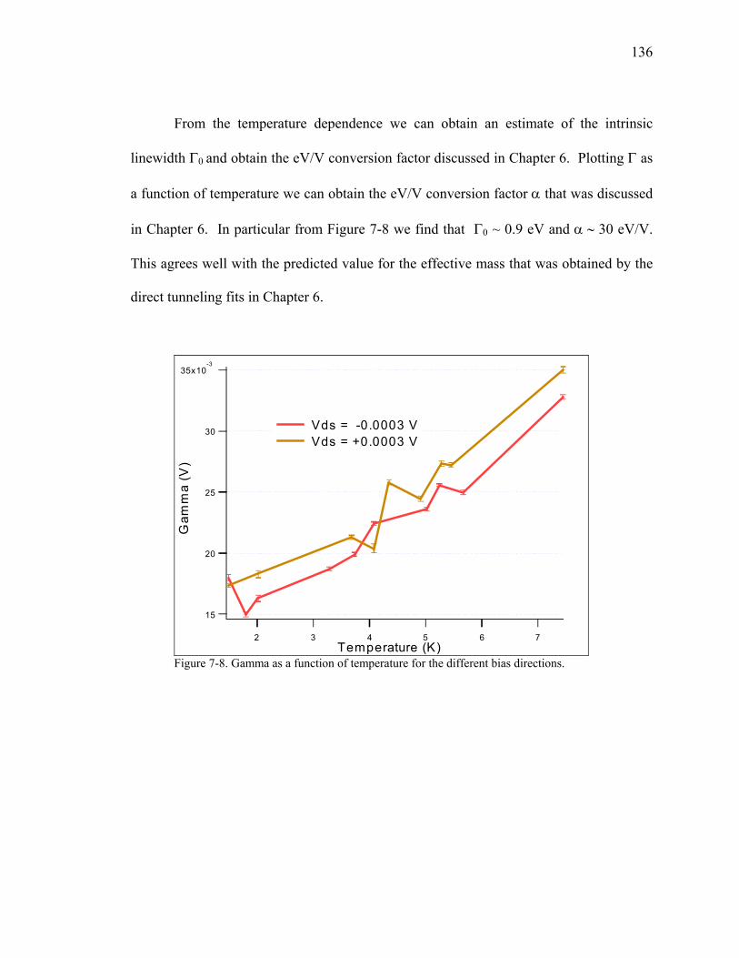
136
From the temperature dependence we can obtain an estimate of the intrinsic
linewidth Γ0 and obtain the eV/V conversion factor discussed in Chapter 6. Plotting Γ as
a function of temperature we can obtain the eV/V conversion factor α that was discussed
in Chapter 6. In particular from Figure 7-8 we find that Γ0 ~ 0.9 eV and α ∼ 30 eV/V.
This agrees well with the predicted value for the effective mass that was obtained by the
direct tunneling fits in Chapter 6.
35x10-3
30
25
20
15
Gam
ma
(V)
765432Temperature (K)
Vds = -0.0003 V Vds = +0.0003 V
Figure 7-8. Gamma as a function of temperature for the different bias directions.

137
-1.864
-1.862
-1.860
-1.858
Ere
s (V
)
765432Temperature (K)
Vds = - 0.0003 + 0.0003
Figure 7-9. Comparison of Eres as a function of temperature for different directions of applied bias.
Next we consider the effect of the temperature on the position of the resonant
width Eres. As the temperature is increased, the amount of bias dropped across the barrier
will change as the relative resistances of the source, drain and channel change. For
different bias directions, we expect the resonance to move in opposite directions, as
shown in Figure 7-9. Note that halfway between the position of Eres for the different
biases is the position of the peak for Vds = 0.
7.5 Bias Dependence
One reason why the results presented in section 7.3 are surprising is that they do not
depend on the direct tunneling transmission coefficient. From conventional diode theory,
and from equations (2.13) and (2.14), we might expect that increasing the bias in either
the positive or negative direction would increase the asymmetry of the two directions
because of the difference between tsm and tms. Instead, the results from Section 7.3
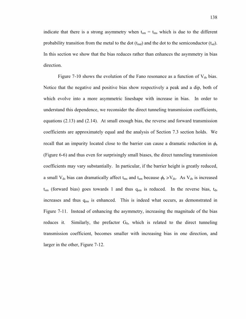
138
indicate that there is a strong asymmetry when tsm = tms which is due to the different
probability transition from the metal to the dot (tmd) and the dot to the semiconductor (tsd).
In this section we show that the bias reduces rather than enhances the asymmetry in bias
direction.
Figure 7-10 shows the evolution of the Fano resonance as a function of Vds bias.
Notice that the negative and positive bias show respectively a peak and a dip, both of
which evolve into a more asymmetric lineshape with increase in bias. In order to
understand this dependence, we reconsider the direct tunneling transmission coefficients,
equations (2.13) and (2.14). At small enough bias, the reverse and forward transmission
coefficients are approximately equal and the analysis of Section 7.3 section holds. We
recall that an impurity located close to the barrier can cause a dramatic reduction in φb
(Figure 6-6) and thus even for surprisingly small biases, the direct tunneling transmission
coefficients may vary substantially. In particular, if the barrier height is greatly reduced,
a small Vds bias can dramatically affect tms and tsm because φb rVds. As Vds is increased
tsm (forward bias) goes towards 1 and thus qsm is reduced. In the reverse bias, tds
increases and thus qms is enhanced. This is indeed what occurs, as demonstrated in
Figure 7-11. Instead of enhancing the asymmetry, increasing the magnitude of the bias
reduces it. Similarly, the prefactor G0, which is related to the direct tunneling
transmission coefficient, becomes smaller with increasing bias in one direction, and
larger in the other, Figure 7-12.
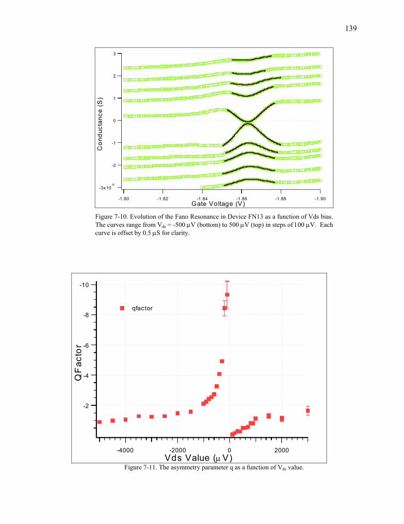
139
-3x10⁻⁶
-2
-1
0
1
2
3
Con
duct
ance
(S)
-1.90-1.88-1.86-1.84-1.82-1.80Gate Voltage (V)
Figure 7-10. Evolution of the Fano Resonance in Device FN13 as a function of Vds bias. The curves range from Vds = -500 µV (bottom) to 500 µV (top) in steps of 100 µV. Each curve is offset by 0.5 µS for clarity.
-10
-8
-6
-4
-2
QF
acto
r
-4000 -2000 0 2000Vds Value (µ V)
qfactor
Figure 7-11. The asymmetry parameter q as a function of Vds value.
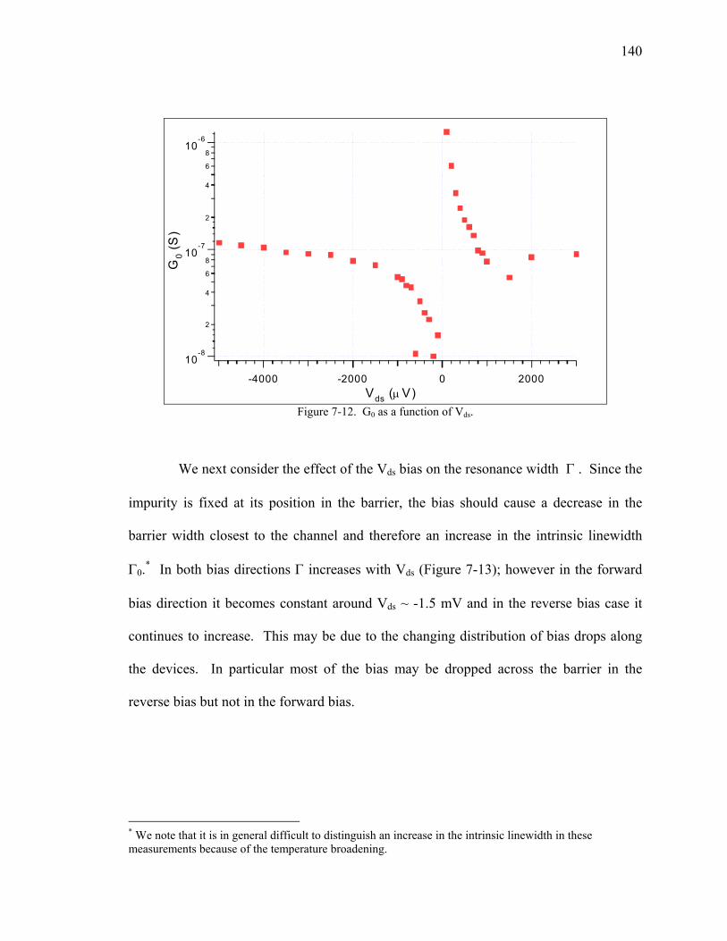
140
10-8
2
4
6
810
-7
2
4
6
810
-6
G0
(S)
-4000 -2000 0 2000Vds (µ V)
Figure 7-12. G0 as a function of Vds.
We next consider the effect of the Vds bias on the resonance width Γ . Since the
impurity is fixed at its position in the barrier, the bias should cause a decrease in the
barrier width closest to the channel and therefore an increase in the intrinsic linewidth
Γ0.* In both bias directions Γ increases with Vds (Figure 7-13); however in the forward
bias direction it becomes constant around Vds ~ -1.5 mV and in the reverse bias case it
continues to increase. This may be due to the changing distribution of bias drops along
the devices. In particular most of the bias may be dropped across the barrier in the
reverse bias but not in the forward bias.
* We note that it is in general difficult to distinguish an increase in the intrinsic linewidth in these measurements because of the temperature broadening.
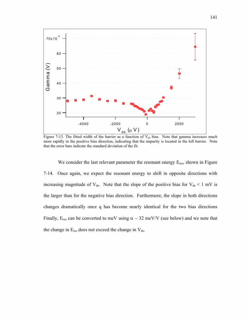
141
70x 10-3
60
50
40
30
20
Gam
ma
(V)
-4000 -2000 0 2000
V ds (µ V ) Figure 7-13. The fitted width of the barrier as a function of Vds bias. Note that gamma increases much more rapidly in the positive bias direction, indicating that the impurity is located in the left barrier. Note that the error bars indicate the standard deviation of the fit.
We consider the last relevant parameter the resonant energy Eres, shown in Figure
7-14. Once again, we expect the resonant energy to shift in opposite directions with
increasing magnitude of Vds. Note that the slope of the positive bias for Vds < 1 mV is
the larger than for the negative bias direction. Furthermore, the slope in both directions
changes dramatically once q has become nearly identical for the two bias directions
Finally, Eres can be converted to meV using α ~ 32 meV/V (see below) and we note that
the change in Eres does not exceed the change in Vds.

142
-1.868
-1.866
-1.864
-1.862
-1.860
-1.858
Ere
s (V
)
-4000 -2000 0 2000Vds Bias (µ V)
Figure 7-14. The resonant energy Eres as a function of bias voltage. Note that the shift in Eres is indicative of the amount of bias dropped across the barrier. The Eres scale is in volts and in order to compare it with the Vds bias should be converted to meV using equation (6.5)
All of the above analysis leads us to another very interesting result, the
observation of an auto-ionized state. An auto-ionized state occurs when, the barrier
between the dot and the semiconductor is reduced so much that the discrete state is no
longer bound, depicted schematically in Figure 7-15. Such a state can only occur in the
reverse bias direction in which the band bending is increased and it is indeed observed
only in the positive bias direction, which corresponds in this case the a reverse bias
through the drain contact. When a state becomes auto-ionized, the direct tunneling
transmission coefficient and the resonant width are suddenly increased because the
probability of transmission has been increased. Note that since q is the ratio of the two
(equation 7.7), it does not change significantly. It is clearly evident in Figures 7-11
through 7-14 for Vds > 2 mV.

143
Depletion width
Dot diameter
Figure 7-15. Schematic indicating how an auto-ionized state can arise.
In this chapter we have seen some interesting consequences of an impurity located
near a metal/semiconductor contact. In particular, it causes a reduction in the barrier
height and an increase in the tunneling locally around the discrete state. At temperatures
low enough to resolve the resonant state, these conditions give rise to Fano interference.
The interference is enhanced when current is transported from the semiconductor to the
metal as compared to the metal to semiconductor. When the bias is larger, this effect is
washed out and the lineshapes move towards an asymmetry of 1.

Chapter 8
Conclusions
Device Physics
We have investigated a novel silicon transistor from both the perspective of practical
applications and interest in a novel solid-state phenomenon. In Chapter 4 device
operation of the SBMOSFET was explored in the temperature range from 200-300 K.
We examined for the first time SBMOSFETs fabricated on bulk silicon that have low off
state leakage currents. In the sub-threshold regime, the transfer characteristics are
dominated by the lowering of the effective Schottky barrier and thermionic emission is
sufficient to describe the transport. By assuming that all of the bias is dropped at the
barriers, we use the carrier concentrations from a MOS capacitor and obtain an expected
effective barrier height. Performing variable temperature measurements, we obtain an
experimental effective barrier and find reasonably good agreement with the predicted
value. One difficulty with these measurements is that the carrier concentration decreases
with temperature, causing the image force lowering and thus the barrier height to vary.
In the on state, our experiments indicate that the dominant transport mechanism in the
channel is due to the transport at the Schottky barrier. Although conventional MOSFET
equations, with some modifications, can accurately describe the transport, in general the
current is limited by the transport at the barrier. In Chapter 5 we investigated the device

145
scaling of SBMOSFETs from 2 µm channel lengths down to 30 nm. The devices
exhibited a substantial degradation in the ideal device characteristics as made smaller.
We find that this is caused by a sub-surface reach-through. Degradation is apparent in
the 700 nm channel length devices and is quite severe for the smallest dimension
transistors.
The research here is certainly a step forward in terms of SBMOSFET device
physics. In particular, we are accurately able to determine the transport properties and
find that they are very comparable to standard MOSFETs. However, there are still many
obstacles to overcome before these devices can be used in practical applications. The
two largest challenges facing SBMOSFETs on bulk silicon are the drive current and the
sub-surface leakage. Increasing the drive current can be achieved by either increasing the
doping in the substrate or decreasing the gate oxide thickness. One solution to the sub-
surface leakage problem is punch-through stoppers. However, if implemented, they may
result in an increase in the electron tunneling current. Another option would be to
engineer the source and drain contacts so that they are highly tapered so that underneath
the channel the contacts define a very small device dimension, but further away the
dimension is much larger. Certainly the simplest solution to both of these problems is to
move to a SOI substrate. The thickness of the substrate could then be ‘tuned’ so that the
drive current is enhanced but the leakage current is reduced.
Fano Resonances
In Chapters 6 and 7 we investigated the low temperature properties of SBMOSFETs. In
particular we observed large reductions in the local Schottky barrier height due to
146
impurities located near the metal/semiconductor interface. Such reductions give rise to
enhanced tunneling and result in non-uniform Schottky barriers. Although this effect is
evident at higher temperatures, it is even more striking at cryogenic temperatures when
the quantum confinement of the impurity gives rise to bound states. In particular, there is
a quantum interference between the resonant states and the continuum which gives rise
both resonant dips and resonant peaks. This structure can not be described by the
Lorentzian lineshape and provides direct evidence that the tunneling through the barrier is
coherent.
The resonant structure can be accurately described using the Fano form. Fano
resonances are characterized by a family of lineshapes that depend on the phase
difference between the direct tunneling and resonant tunneling paths. In this system, we
find that increasing the temperature and the Vds bias gives rise to ‘tuning’ of the
interference. This is different from standard resonant tunneling experiments in which
increasing the temperature only broadens the linewidth of the resonant state.
The abruptness of the metal/semiconductor contact has a profound effect on the
lineshape for small biases in opposite directions. In particular, we show that resonant
peaks are transformed into dips when the bias is reversed and vice versa. This is a
consequence of the impurity being located asymmetrically in the barrier. In the reverse
bias direction where a dip is exhibited at small biases, increasing the magnitude of the
bias results in a transformation into more asymmetric lineshape due to an increase in the
probability of transition from the dot to the semiconductor. Similarly, in the forward bias
direction, where a peak is observed at small biases, increasing the bias voltage causes an
increase in the direct tunneling transition coefficient and thus a decrease in the

147
asymmetry parameter. In the reverse bias direction, the barrier between the dot and the
semiconductor can be reduced so much that the resonant state is no longer bound and an
auto-ionized state is formed.
Fano resonances in SBMOSFETs differ substantially from most of the previous
work on quantum interference in mesoscopic systems. Most importantly we can neglect
electron-electron interactions so that the physics is much simpler. The system is very
small compared to artificially fabricated alternatives and thus interference is a dominant
component of the transport at low temperatures. The most striking result is that the
abruptness of the contacts gives rise to an asymmetry in the lineshape in opposite bias
directions. This research is conceptually very interesting because it replicates atomic
physics experiments from the 1960’s and 1970’s, but in solid-state system where
different parameters can be varied enabling research into previously unexplored regimes.
Bibliography
Abrahams, E., P.W. Anderson, D.C. Licciardello and T.V. Ramakrishnan. Phys Rev.
Lett. 42, 673 (1979).
Anderson, P.W. Phys. Rev. Lett. 109, 673 (1958).
Ando, T., A.B. Fowler and F. Stern. Rev Mod Phys, 54, 437 (1982).
Andrews, J.M. and M.P. Lepselter. Solid-St. Electron. 13 1011 (1970a).
Andrews, J.M. and T.O. Yep. J. Appl. Phys. 41 303 (1970b).
Bagwell, P.F. Phys Rev B15 10354 (1990).
Bagwell, P.F. and R.K. Lake. Phys Rev B46, 15329 (1992).
Bardeen, J. Phys. Rev. 71 717 (1947).
Beenakker, C.W. J. and H. van Houten. “Quantum Transport in Semiconductor
Nanostructures” in Solid State Physics vol. 44, ed. H. Ehrenreich and D. Turnbull.
New York: Academic Press (1991).
Bending, S.J. and M.R. Beasley. Phys. Rev. Lett. 55 324 (1985).
Cerdeira, F. T.A. Fjeldly, and M. Cardona. Phys Rev. B 8 4734 (1973).
Chang, C.Y., and S.M. Sze. Solid-St. Electron. 13, 727 (1970).
Chin, V.W. L., M.A. Green and J.W. V. Storey. Solid-St. Electron. 36, 1107 (1993).
Chu, C.S. and R.S. Sorbello. Phys Rev B40, 5941 (1989).

149
Clerk, A.A., X. Waintal, and P.W. Brouwer, ArXiv:cond-mat\0010038, (2000).
Crowell, C.R. and S.M. Sze. Solid-St. Electron. 9, 1035 (1966).
Crowell, C.R. Solid-St. Electron. 12, 55 (1969).
Datta, S. Electronic Transport in Mesoscopic Systems, Cambridge University Press: New
York, 1995.
Davidov, B. J. Tech. Phys. USSR 5, 87 (1938).
Dellow, M.W., P.H. Beton, C.J.G.M. Langerak, T.J. Foster, P.C. Main, L.Eaves, M.
Henini, S.P. Beaumont, and C.D.W. W. Wilkinson. Phys. Rev. Lett. 68 1754,
1992.
Deshpande, M.R., E.S. Hornbeck, P.Kozodoy, N.H. Dekker, J.W. Sleight, M.A. Reed,
C.L. Fernando and W.R. Frensley. Semicond. Sci. Technol 9 1919 (1994).
Deshpande, M.R., J.L. Huber, N.H. Dekker, P. Kozodoy, J.W. Sleight, M.A. Reed, C.L.
Fernando, W.R. Frensley, R.J. Matyi and Y.C. Kao. 22 International Conference
on the Physics of Semiconductors. Vancouver, Canada, August 1994. Proceedings
p. 1899, edited by D.J. Lockwood, World Scientific, Singapore 1995.
Deshpande, M.R, J.W. Sleight, M.A. Reed and R.G. Wheeler. Phys Rev. Lett. 76, 1328
(1996).
Desphpande, M.R. Single Electron Tunneling Through Discrete Semiconductor Impurity
States, Ph.D. Dissertation, Yale University, 1998.
Edwards, J.T., and D.J. Thouless. J. Phys. C 5, 807 (19972).
Eugster, C.C., J. A. del Alamo, M. R. Melloch and M.J. Rooks. Phys Rev B46, 10146
(1992).
Fano, U. Phys Rev 124, 1966 (1961).
150
Fano, U. and J.W. Cooper. Rev. Mod. Phys. 40, 441(1968).
Faist, J., P. Guéret and H. Rothuizen. Phys. Rev B42 3217 (1990).
Faist, J., C. Sirtori, F. Capasso, S. N. G. Chu, L. N. Pfeiffer, K.W. West. Opt. Lett. 21,
985 (1996).
Fowler, A.B., A. Hartstein and R.A. Webb. Phys Rev. Lett. 48, 196 (1982).
Fowler, A.B., G.L. Timp, J.J. Wainer and R.A. Webb. Phys. Rev. Lett. 57, 138 (1986).
Fowler, A.B., J.J. Wainer and R.A. Webb. IBM J. Res. Develop. 32, 372 (1988).
Goldhaber, D., J. Göres, M.A. Kastner, H. Shtrikman, D. Mahalu, and U. Meirav. Phys
Rev. Lett 81, 5225 (1998a).
Goldhaber, D., H. Shtrikman, D. Mahalu, D. Abusch-Magder, U. Meirav, and M.A.
Kastner. Nature 391, 156 (1998b)
Göres, J., D. Goldhaber-Gordon, S. Heemeyer, M.A. Kastner, H. Shtrikman, D. Mahalu
and U. Meirav. Phys Rev. B 62, 2188 (2000).
Gurvitz, S.A. and Y.B. Levinson. Phys. Rev. B47, 10578 (1993).
Hareland, S.A., A.F. Tasch and C.M. Maziar. Electronics. Lett. 29, 1894 (1993).
Harrison, W.A. Solid State Theory, New York: Dover, 1979.
Haveemeyer, S. Interference in Resonant Tunneling Through a SET, Ph.D. Dissertation,
MIT, 2000.
Huang, C.K., W.E. Zhang, C.H. Yang. IEEE Trans ED-45, 842 (1998).
Holfeld, C.P., F. Loeser, M. Sudzius, K. Leo, D.M. Whittaker, and K. Koehler. Phys Rev.
Lett. 81, 874 (1998).
Ibach, H. and H. Lüth. Solid State Phyics, New York: Springer-Verlag, 1991.
151
Ieong, M., P.M. Solomon, S.E. Laux, H.S. P. Wong, D. Chidambarrao. IEDM-98, 733
(1998).
The International Technology Roadmap for Semiconductors, Semiconductor Industry
Association, San Jose, CA (1999).
Imry, Y. Introduction to Mesoscopic Physics, Oxford University Press: New York, 1997.
Ishikuro, H. T. Fujii, T. Saraya, G. Hashiguchi, T. Hiramoto and T. Ikoma. Appl. Phys.
Lett. 68, 3585 (1996).
Ivanov, T. and V. Valtchinov. Phys. Rev. B50, 5721 (1994).
Kim, C.S., A.M. Satanin, Y.S. Joe and R.M. Cosby. Phys Rev B60, 10962 (1999).
Kang, W.-T., J.S. Kim, K.-Y. Lee, Y.-C. Shin, T.-H. Kim, Y.-J. Park, and J.-W. Park.
IEEE-EDL, 21, 9, (2000).
Kelly, M.J. Low Dimensional Semiconductors, New York: Oxford, 1995.
Kedzierski, J. P. Xuan, V. Subramanian, J. Bokor, T.-J. King, C.Hu and E. Anderson.
Superlatt. and Microst. 28, 445 (2000).
Kedzierski, J. P. Xuan, V. Subramanian, J. Bokor, T.-J. King, C.Hu and E. Anderson.
IEDM (2000).
Kittel, C. and H. Kroemer. Thermal Physics, 2nd Edition. New York: W.H. Freeman
1980.
Koch, R.H. and A. Hartstein. Phys Rev. Lett. 54, 1848 (1985).
Koeneke, C.J., S.M.Sze, R.M. Levin and E. Kinbron. IEDM 367 (1981).
Kohn, W. “Shallow Impurity States in Silicon and Germanium”, in Solid State Physics,
vol 5, 1957.
Kopley, T.E., P.L. McEuen, and R.G. Wheeler. Phys Rev Lett 61, 1654 (1988).

152
Kopley, T.E. Resonant Tunneling in MOS Devices, Ph.D. Dissertation, Yale University
1989.
Kouwenhoven, L. P. and P.L. McEuen. “Single Electron Transport Through a Quantum
Dot” in Nanotechnology, ed. G. Timp, New York: Springer Verlag, 1999.
Kravchenko, S.V., G.V. Kravchenko, J.E. Furneaux, V.M. Pudalov and M. D’Iorio. Phys
Rev. B50 8039 (1994).
Kuznetsov, V.V., A.K. Savchenko, M.E. Raikh, L.E. Glazman, D.R. Mace, E.H. Linfield,
and D.A. Ritchie. Phys Rev B 54, 1502 (1996).
Kuznetsov, V.V. and A.K. Savchenko, D.R. Mace, E.H. Linfield, and D.A. Ritchie. Phys
Rev B 56, R15533 (1997).
Landau, L.D. and E.M. Lifshitz. Quantum Mechanics (Non-relativistic Theroy), New
York: Pergamon, 1994.
Lee, K., M. Sur, T.A. Fjeldly and T. Ytterdal. Semiconductor Device Modeling for VLSI,
NJ: PrenticeHall; 1993.
Lepselter, M.P., and S.M. Sze, Bell Syst. Tech. J. 47, 195 (1968).
Lepselter, M.P., and S.M. Sze. Proc. IEEE 56, 1400 (1968).
Li, J., W.-D. Schneider, R. Berndt, and B. Delley. Phys. Rev. Lett. 80, 2893 (1998).
Lundstrom, M. and S. Tanaka. “Carrier Transport in Metal/Semiconductor Junctions
Revisited”, preprint Purdue University, Indiana, 1996.
Madhaven, V., W. Chen, T. Jamneala, M.F. Crommie, and N.S. Wingreen. Science 280,
567 (1998).
Manoharan, H.C., C.P. Lutz, and D.M. Eigler. Nature 403, 512 (2000).
Mateev, K.A. and A.I. Larkin. Phys Rev B, 46, 15,337 (1992).

153
McCafferty, P.G. A. Sellai, P. Dawson and H. Elabd. Solid-St. Electron. 39, 583 (1996).
McEuen, P., B.W. Alphenaar and R.G. Wheeler. Surface Science 229, 312(1990).
McEuen, P. Transport in One Dimensional Systems, Ph.D.Dissertation, Yale University,
1991.
Meir, Y. Phys Rev Lett 83, 3506 (1999).
Muller, R.S. and T.I. Kamins. Device Electronics for Integrated Circuits, New
York:Wilely, 1986.
Murarka, S.P. Silicides for VLSI Applications, New York: Academic Press, 1983.
Nicollian, E.H. and J.R. Brews. MOS Physics and Technology, New York: John Wiley &
Sons, 1982.
Nöckel, J.U. Phys. Rev. B 46, 15,348 (1992).
Nöckel, J.U. and A.D. Stone. Phys. Rev. B 50, 17,415 (1994).
Nöckel, J.U. and A.D. Stone. Phys. Rev. B 51, 17,219 (1995).
Oberlie, D.Y. et al. Phys Rev B 49, 5757 (1994).
Padovani, F.A., and R. Stratton. Solid-St Electron. 9 695 (1966).
Padovani, F.A. “The Voltage-Current Characteristic of Metal-Semiconductor Contacts”,
in Semiconductor and Semimetals, ed. Willardson and Beer, Academic Press:
New York; 1971, p. 75.
Pierret, Semiconductor Device Physics, John Wiley & Sons: New York; 1996
Porod, W., Z. Shao, and C.S. Lent. Appl Phys Lett. 61 1350 (1992).
Ralph, D.C., A.W.W. Ludwig, J.von Delft and R.A. Buhrman. Phys Rev. Lett 72, 1064
(1994a).
Ralph, D.C. and R.A. Buhrman. Phys Rev. Lett 72, 3401 (1994b).

154
Ricco, and Y. Azbel. Phys. Rev. B29 1970 (1984).
Rideout, V.L., and C.R. Crowell. Solid-St. Electron, 13, 993 (1970).
Rishton, S.A., K. Ismail, J.O. Chu and K. Chan. Microelectron. Eng. 35, 361 (1997).
Rhoderick, E.H. and R.H. Williams. Metal-Semiconductor Contacts. London:Oxford;
1988.
Ryu, C-M and S.Y. Cho. Phys Rev B58, 3572 (1998).
Saitoh, W., S. Yamagami, A. Itoh and M. Asada. DRC June 28-29, 1999.
Saitoh, W., S. yamagami,A. Otoh and M.Asada. Jpn. J. Appl. Phys. 38 L629 (1999).
Sanquer, M., M. Specht, L. Ghenim, S. Deleonibus and G. Guegan. Phys. Rev. B 61,
7249 (2000)
Savchenko, A., V.V. Kuznetsov, A. Woolfe, D.R. Mace, M. Pepper, D.A. Ritchie, and
G.A. C. Jones. Phys Rev B52, R17021 (1995).
Schulz, G. Rev. Mod Phys 45, 378 (1973).
Schuster, R., E. Buks, M. Heiblum, D. Mahalu, V. Umansky and H. Shtrikman. Nature
385 417 (1997).
Scott-Thomas, J.H.F., S. B. Field, M.A. Kastner, I. Smith, and D.A. Antoniadis. Phys.
Rev. Lett. 61, 1167 (1989).
Shao, X. W. Porod and C. S. Lent. Phys Rev B49, 7453 (1994).
Smith, K. Rep. Prog. Phys 29, 373 (1966).
Snyder, J.P., C.R. Helms, Y.Hishi. Appl. Phys. Lett. 67, 1420 (1995).
Snyder, J.P., C.R. Helms, Y.Hishi. Appl. Phys. Lett. 74, 3407 (1999).
Stratton, R. J. Phys. Chem. Solids 23, 1177-1190 (1962).
Sze, S.M., D.J. Coleman, A. Loya. Solid-St. Electron 14, 1209 (1971).

155
Sze, S.M. The Physics of Semiconductor Devices, 2nd Edition. John Wiley & Sons: New
York; 1981.
Sze, S.M., ed. Modern Semiconductor Device Physics, John Wiley & Sons: New York,
1998.
Tekman, E. and P. Bagwell. Phys Rev B 48, 2553 (1993).
Tucker, J.R., C. Wang and P. Scott Carney. Appl. Phys. Lett. 67, 1420 (1995).
Tung, R.T. Phys Rev. Lett 84, 6078 (2000).
Von Klitzing, K. G. Landwehr and G. Dorda. Japan. J. Appl. Phys, Suppl. 2, Pt. 2, 351
(1974a).
Von Klitzing, K. and G. Landwehr. Solid-St. Commun. 15, 489 (1974b).
Wees, B.J., H. van Houten, C.W. Beenakker, J.G. Williamson, L.P. Kouwenhoven, D.
Van der Marcel and C.T. Foxon. Phys. Rev.Lett. 60, 848 (1988).
Van Houten, H., C.W. J. Beenakker and B.J. van Wees. ‘Quantum Point Contacts’ in
Semiconductors and Semimetals, vol. 35, ed. M. A. Reed. New York: Academic
Press (1992).
Wang, C. A Sub-0.1 µm PtSi Schottky Source/Drain MOSFET. Ph.D. Dissertation,
University of Illinois at Urbana-Champaign, 1998.
Wang, C., J.P. Snyder, J.R. Tucker. Appl. Phys. Lett. 74, (1999).
Wilson, A.H. Proc. Roy. Soc. (London) A136, 487 (1932).
Wolf, S. Silicon Processing for the VLSI Era: Vol. 3 The Submicron MOSFET. Sunset
Beach, CA: Lattice Press; 1995.
Xu, H. and W. Sheng. Phys Rev B57 11903 (1998).
Yacoby, A., M. Heiblum, D. Mahalu and H. Shtrikman. Phys. Rev. Lett. 74 4047 (1995).
156
Zacharia, I.G., D. Goldhaber-Gordon, G. Granger, M.A. Kastner, Yu. B. Khavin, H.
Shtrikman, D.Mahalu and U. Meirav. ArXiv:cond-mat\0009140v2, (2000).
Zhang, L. L. Guo and S.Y. Chou. Appl.Phys. Lett. 72, 1205 (1998).
Zhao, Q.T, F. Klinkhammer, M. Dolle, L. Kappius, and S. Mantl. Appl. Phys. Lett., 74,
(1999).
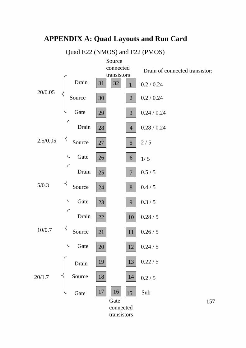
157
Quad E22 (NMOS) and F22 (PMOS)Sourceconnectedtransistors
Gateconnectedtransistors
32
2
3
4
5
6
7
8
9
10
11
12
13
14
16
31
30
29
28
27
26
25
24
23
22
21
20
19
18
17
1
15 SubGate
20/1.7
Drain
Source
Gate
10/0.7
Drain
Source
Gate
5/0.3
Drain
Source
Gate
2.5/0.05
Drain
Source
20/0.05
Gate
Drain
Source
APPENDIX A: Quad Layouts and Run Card
Drain of connected transistor:
0.2 / 0.24
0.2 / 0.24
0.24 / 0.24
0.28 / 0.24
2 / 5
1/ 5
0.5 / 5
0.4 / 5
0.3 / 5
0.28 / 5
0.26 / 5
0.24 / 5
0.22 / 5
0.2 / 5

158
Quad E23 (NMOS) and F23 (PMOS)
Sourceconnectedtransistors
Gateconnectedtransistors
32
2
3
4
5
6
7
8
9
10
11
12
13
14
16
31
30
29
28
27
26
25
24
23
22
21
20
19
18
17
1
15 Sub
0.26 / 0.24
0.2 / 0.21
0.20 / 0.24
0.20 / 0.27
20/ 0.3
20/ 0.38
20/ 5
20 / 1
20 /1. 5
20 / 2
20 / 5
20 / 20
0.6 / 20
0.3 / 20
0.3 / 0.24
0.6 / 0.21
3 / 0.24
0.3 / 0.3
3/ 0.3
0.3/ 0.38
0.6/ 0.5
0.3 / 0.5
0.3 /1
0.3 / 1.5
3 / 1.5
0.3 / 2
0.6 / 5
3 / 20
0.26 / 20
Drain of connected transistor:
Drain of connected transistor:
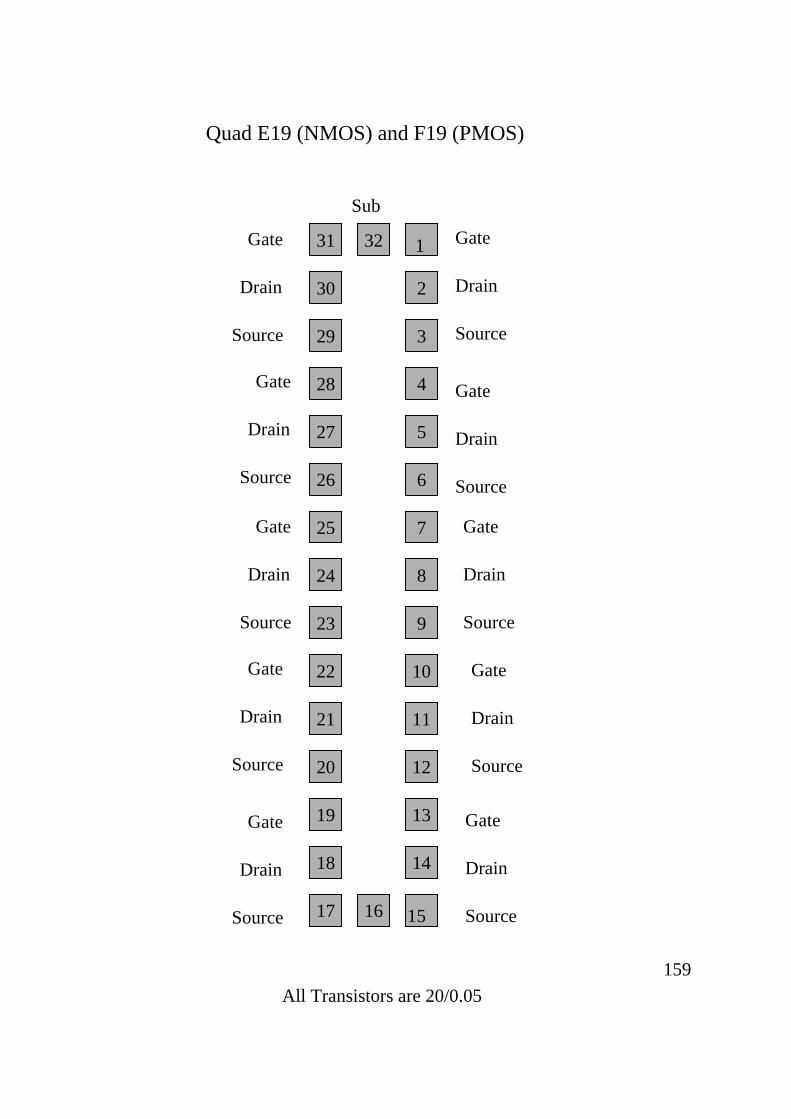
159All Transistors are 20/0.05
32
2
3
4
5
6
7
8
9
10
11
12
13
14
16
31
30
29
28
27
26
25
24
23
22
21
20
19
18
17
1
15
Sub
Gate
Drain
Source
Gate
Drain
Source
Gate
Drain
Source
Gate
Drain
Source
Gate
Drain
Source
Gate
Drain
Source
Gate
Drain
Source
Gate
Drain
Source
Gate
Drain
Source
Gate
Drain
Source
Quad E19 (NMOS) and F19 (PMOS)

160
Quad C05 and C06
Cap 1
Cap 1
Cap 2
Cap 2
N 0.3
N 0.4
P 0.3
P 0.4
Combs
Capacitors are 100 µm2
32
2
3
4
5
6
7
8
9
10
11
12
13
14
16
31
30
29
28
27
26
25
24
23
22
21
20
19
18
17
1
15

161
PTA NTBProcess Details 1
(P2 3 4 5 6 7 8 9 10 11 12 13 14 15 16 17 18 1 2 3 4 5 6 7 8 9 10 11 12 13 14 15 16 17 18 19
p- bulk wafers p- 3-20?-cm B-doped n- bulk wafers n- 3-22?-cm P-dopedpre-oxidation clean isolation oxide 1 isolation oxide 2 isolation oxidenom. 725Å spin/exp/dev interface 70122, 12200Åtrench etch nom. 1200Å into Si, 120s sulfuric cleanspin/exp/dev 34mJ/cm2 +0.3umtimed oxide etch73-75s CF4 sulfuric cleansacrificial oxidegate oxidation 35Å 50/50 N20/O2 35Å N2O only 20Å N2O onlypoly deposition undoped a-Si1200Å undoped a-Si n+ a-Si depos1200Å in-situ-doped n+ a-Sipoly implant p+ implant boron 5keV 5e15/cm3spin/exp/dev 29mJ/cm2 +0.2umetch poly strip resistbackside poly/oxide etch poly RTO 15s 1100°C, 130Å nom. poly RTO 50s 1000°C, 130Å nom. poly RTO 6s 1100°C, 100Å nom.spacer/Si etch spacer/Si etch15s, 225Å nom. spacer/Si etch20s, 300Å nom.backside oxide etchclean piranha & 30min SC1HF dip <20Å oxide removal Pt deposition 9?/sq Pt deposition 7?/sqPt silicidation 60min 450°Caqua regia strip strip unreacted Pt, 85°C, 10min IPA washbottle SC1 clean PETEOS/PEP500Å PETEOS & 1000Å PEPSG PETEOS/SAP500Å PETEOS & 1000Å SAPSGspin/exp/dev 65s split 65s 70s split 70s 75s split 75s ash solvent clean SC1 clean use fresh SC1 75Å presputte75Åsputter,600ÅTiN,4500ÅAlCu,250ÅTiNspin/exp/devM1 etch 30s resist stripforming gas anneal
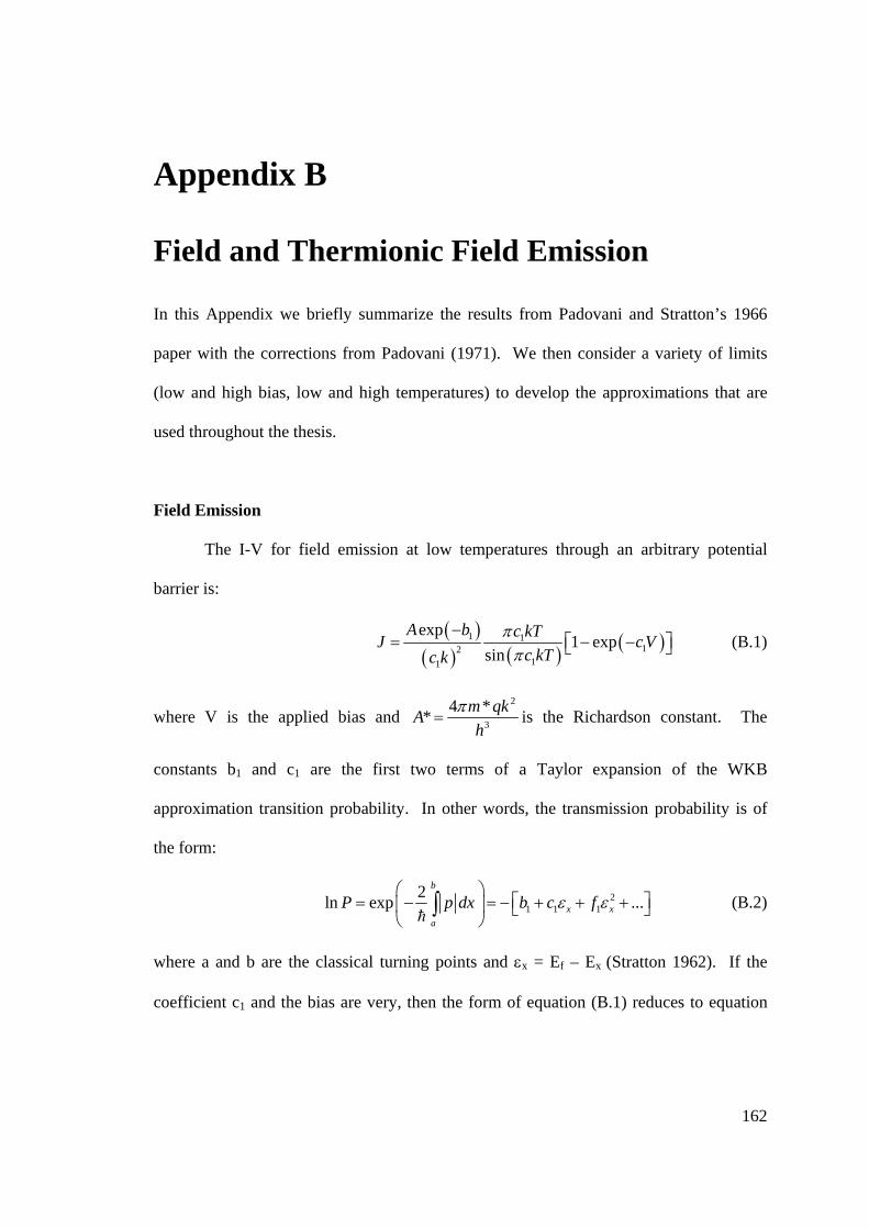
162
Appendix B
Field and Thermionic Field Emission
In this Appendix we briefly summarize the results from Padovani and Stratton’s 1966
paper with the corrections from Padovani (1971). We then consider a variety of limits
(low and high bias, low and high temperatures) to develop the approximations that are
used throughout the thesis.
Field Emission
The I-V for field emission at low temperatures through an arbitrary potential
barrier is:
( )( ) ( ) ( )1 1
1211
exp1 exp
sinA b c kTJ cV
c kTc kπ
π−
= − −⎡ ⎤⎣ ⎦ (B.1)
where V is the applied bias and 2
3
4 ** m qkAh
π= is the Richardson constant. The
constants b1 and c1 are the first two terms of a Taylor expansion of the WKB
approximation transition probability. In other words, the transmission probability is of
the form:
21 1 1
2ln exp ...b
x xa
P p dx b c fε ε⎛ ⎞
⎡ ⎤= − = − + + +⎜ ⎟ ⎣ ⎦⎝ ⎠
∫h (B.2)
where a and b are the classical turning points and εx = Ef – Ex (Stratton 1962). If the
coefficient c1 and the bias are very, then the form of equation (B.1) reduces to equation

163
(2.17), where the coefficient b is the Fowler-Nordheim transmission probability for a
triangular barrier. The field emission equation is valid when
1/ 21 11 (2 )c kT kT f− > (B.3)
The paper then proceeds to determine b1, c1 and f1 for forward and reverse bias. The
results are:
Forward bias: ( )
100
B dsVb
Eφ −
=
( )1
00
41 ln2
b dsVc
Eφ
ξ−⎡ ⎤
= ⎢ ⎥⎣ ⎦
1 0014
f E ξ=
Figure B-1. Schematic of Forward bias M-S contact.
Reverse bias:
( ) ( ) ( )( )
1/ 2 1/ 21/ 21/ 2
1 1/ 200
1 ln b ds bb b ds ds
ds
Vb V V
E Vφ ξ φ
φ φ ξ ξξ
⎧ ⎫⎡ ⎤− + +⎪ ⎪= − + + − ⎢ ⎥⎨ ⎬−⎢ ⎥⎪ ⎪⎣ ⎦⎩ ⎭
( )1 0014 dsf E Vξ= −
Figure B-2. Schematic of Reverse bias M-S contact
where 00 2 *s
q NEmε
=h , and ξ is defined in Figure A-1 above. We note that there are
several mistakes and approximations in the original paper and that the expressions for the
coefficients above are taken from Padovani 1971.
( )( )
1/ 2 1/ 2
1 1/ 200
1 ln b ds b
ds
Vc
E Vφ ξ φ
ξ
⎡ ⎤− + += ⎢ ⎥
− +⎢ ⎥⎣ ⎦
qφb
qVds ξ
qφb qVds F
Emission
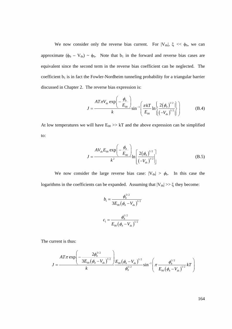
164
We now consider only the reverse bias current. For |Vds|, ξ << φb, we can
approximate (φb – Vds) ~ φb. Note that b1 in the forward and reverse bias cases are
equivalent since the second term in the reverse bias coefficient can be neglected. The
coefficient b1 is in fact the Fowler-Nordheim tunneling probability for a triangular barrier
discussed in Chapter 2. The reverse bias expression is:
( )( )
1/ 200 1
1/ 200
exp2
sin ln
bds
b
ds
AT VE kTJ
k E V
φπφπ−
⎛ ⎞−⎜ ⎟ ⎛ ⎞⎧ ⎫⎪ ⎪⎝ ⎠ ⎜ ⎟= ⎨ ⎬⎜ ⎟−⎪ ⎪⎩ ⎭⎝ ⎠
(B.4)
At low temperatures we will have E00 >> kT and the above expression can be simplified
to:
( )( )
1/ 20000
1/ 22
exp2
ln
bds
b
ds
AV EE
Jk V
φφ
⎛ ⎞−⎜ ⎟ ⎡ ⎤⎝ ⎠= ⎢ ⎥
−⎢ ⎥⎣ ⎦ (B.5)
We now consider the large reverse bias case: |Vds| > φb. In this case the
logarithms in the coefficients can be expanded. Assuming that |Vds| >> ξ they become:
( )
3/ 2
1 1/ 2003
b
b ds
bE V
φφ
=−
The current is thus:
( ) ( )( )
3/ 2
1/ 2 1/ 2 1/ 200 00 1
1/ 21/ 200
2exp3
sin
b
b ds b ds b
b b ds
ATE V E V
J kTk E V
φπφ φ φπ
φ φ−
⎛ ⎞−⎜ ⎟⎜ ⎟ ⎛ ⎞− −⎝ ⎠= ⎜ ⎟
⎜ ⎟−⎝ ⎠
( )
1/ 2
1 1/ 200
b
b ds
cE V
φφ
=−
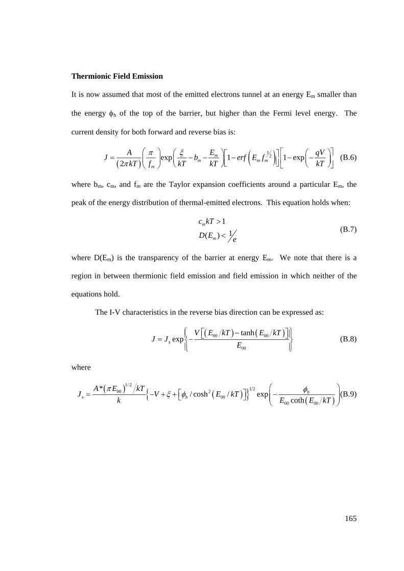
165
Thermionic Field Emission
It is now assumed that most of the emitted electrons tunnel at an energy Em smaller than
the energy φb of the top of the barrier, but higher than the Fermi level energy. The
current density for both forward and reverse bias is:
( ) ( )12exp 1 1 exp
2m
m m mm
EA qVJ b erf E fkT f kT kT kT
π ξπ
⎛ ⎞ ⎡ ⎤⎛ ⎞ ⎛ ⎞⎡ ⎤= − − − − −⎜ ⎟ ⎜ ⎟⎜ ⎟ ⎢ ⎥⎢ ⎥⎣ ⎦ ⎝ ⎠⎝ ⎠ ⎣ ⎦⎝ ⎠ (B.6)
where bm, cm, and fm are the Taylor expansion coefficients around a particular Em, the
peak of the energy distribution of thermal-emitted electrons. This equation holds when:
1
1( )m
m
c kT
D E e
>
< (B.7)
where D(Em) is the transparency of the barrier at energy Em. We note that there is a
region in between thermionic field emission and field emission in which neither of the
equations hold.
The I-V characteristics in the reverse bias direction can be expressed as:
( ) ( )00 00
00
tanhexps
V E kT E kTJ J
E
⎧ ⎫−⎡ ⎤⎪ ⎪⎣ ⎦= −⎨ ⎬⎪ ⎪⎩ ⎭
(B.8)
where
( ) ( ) ( )
1/ 21 200 2
0000 00
*/ cosh / exp
cothb
s b
A E kTJ V E kT
k E E kTπ φξ φ
⎛ ⎞⎡ ⎤= − + + −⎜ ⎟⎣ ⎦ ⎜ ⎟
⎝ ⎠(B.9)