Embed Size (px)
Citation preview
FEATURE ARTICLE www.rsc.org/materials | Journal of Materials Chemistry
Electrochemically functionalized carbon nanotubes for device applications
Kannan Balasubramanian and Marko Burghard
Received 26th November 2007, Accepted 4th February 2008
First published as an Advance Article on the web 3rd March 2008
DOI: 10.1039/b718262g
The application range of carbon nanotubes (CNTs) has been significantly expanded by the advent of
reliable chemical functionalization methods. This article surveys electrochemistry-based approaches
that have been devised for the covalent and non-covalent modification of CNTs, and highlights their
increasing importance in the development of nanoscale and macroscopic CNT devices. The primary
focus is on electrochemical protocols for selective functionalization of CNTs according to their
electronic properties, as well as the fabrication of various types of CNT-based sensors for gases and
(bio)molecules.
1. Introduction
The prospects for the application of carbon nanotubes (CNTs)
are multi-faceted ranging from reinforced composites to molec-
ular-scale electronic devices. While most of the applications still
remain a far-off dream, a number of such promises have been
successfully realized such as field-emission displays1 and
scanning probe tips.2 Moreover, CNTs have been successfully
implemented as highly efficient conduction channels into field-
effect transistors (FETs). However, although the first CNT-
FETs were demonstrated one decade ago,3,4 the integration of
such devices as integral components of computers still remains
to be achieved. While efforts are undertaken to reach this goal,
optimized device architectures are constantly emerging5 and
the basic understanding of the physics of CNT-FETs is steadily
expanding.6,7 In this context, the development of reliable CNT
chemical functionalization strategies has significantly contrib-
uted to the progress.8–11 The present review focuses on one
specific type of functionalization method, namely the electro-
chemical route. After a brief introduction about carbon
nanotubes in general and their reactivity, the available electro-
chemical functionalization schemes are outlined. The subsequent
Dr Kannan Balasubramanian
Kannan Balasubramanian
obtained his PhD in Nanostruc-
ture Physics from the EPFL,
Switzerland in 2005 by working
at the Max-Planck-Institute
for Solid State Research, where
he is currently leading a junior
research group on Nanoscale
Diagnostics. His interests
include the use of functionalized
1D nanostrucutures as sensors
for applications in medical diag-
nosis.
Max-Planck-Institut fuer Festkoerperforschung, Heisenbergstrasse 1,D-70569 Stuttgart, Germany
This journal is ª The Royal Society of Chemistry 2008
section is devoted to the fabrication of CNT-FETs through
selective electrochemical elimination of metallic nanotubes.
Following this, the application of electrochemically functional-
ized CNTs as detectors for gas molecules and as sensors for
analytes in liquid solutions will be presented. The review
concludes with future perspectives for devices based on electro-
chemically functionalized CNTs.
2. Carbon nanotubes
2.1 Electronic and physical structure
Carbon nanotubes are rolled-up graphene sheets occurring as
single-wall (SWCNT) or multi-wall (MWCNT) cylinders.12
They have diameters from 0.4 up to a few nm, and their lengths
range from a few nanometres up to several millimetres. Any
single SWCNT can be specified by its chiral vector (n,m), which
in turn determines the tube’s electronic structure.12 The diameter
of an (n,m) tube is given by d ¼ ap
ffiffiffiffiffiffiffiffiffiffiffiffiffiffiffiffiffiffiffiffiffiffiffiffiffiffiffiffiffiffiffiffiðn2 þ nmþm2Þ
p, where the
lattice constant a is related to the nearest-neighbour bond
distance (ac–c) between two carbon atoms through a ¼ O3ac–c¼ O3 � 1.42 A ¼ 2.46 A. In general, (n,m)-SWCNTs with
(n,m) being an integer multiple of 3 are metallic (m-SWCNTs)
or semi-metallic, whereas all other tubes are semiconducting
(s-SWCNTs). The band-gap of an s-SWCNT can be approxi-
mated to 0.8 eV/d,13 where d is the diameter of the nanotube in
Dr habil: Marko Burghard
Marko Burghard received his
PhD from the Institute for Phys-
ical Chemistry at the University
of Tuebingen. Then he joined the
Max-Planck Institute for Solid
State Research, where he
worked on thin organic films
for applications in molecular
electronics. Since 2000 his
primary focus has been on the
electrical and optical properties
of different types of chemically
functionalized nanowires.
J. Mater. Chem., 2008, 18, 3071–3083 | 3071
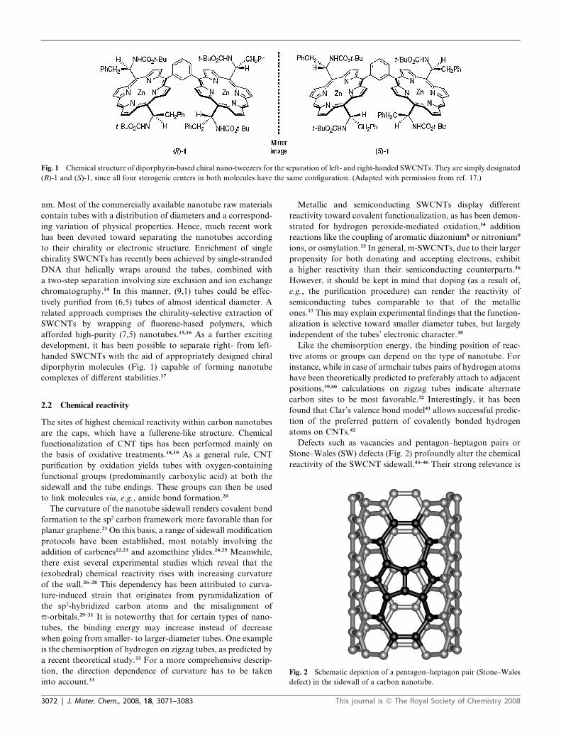
Fig. 1 Chemical structure of diporphyrin-based chiral nano-tweezers for the separation of left- and right-handed SWCNTs. They are simply designated
(R)-1 and (S)-1, since all four sterogenic centers in both molecules have the same configuration. (Adapted with permission from ref. 17.)
nm. Most of the commercially available nanotube raw materials
contain tubes with a distribution of diameters and a correspond-
ing variation of physical properties. Hence, much recent work
has been devoted toward separating the nanotubes according
to their chirality or electronic structure. Enrichment of single
chirality SWCNTs has recently been achieved by single-stranded
DNA that helically wraps around the tubes, combined with
a two-step separation involving size exclusion and ion exchange
chromatography.14 In this manner, (9,1) tubes could be effec-
tively purified from (6,5) tubes of almost identical diameter. A
related approach comprises the chirality-selective extraction of
SWCNTs by wrapping of fluorene-based polymers, which
afforded high-purity (7,5) nanotubes.15,16 As a further exciting
development, it has been possible to separate right- from left-
handed SWCNTs with the aid of appropriately designed chiral
diporphyrin molecules (Fig. 1) capable of forming nanotube
complexes of different stabilities.17
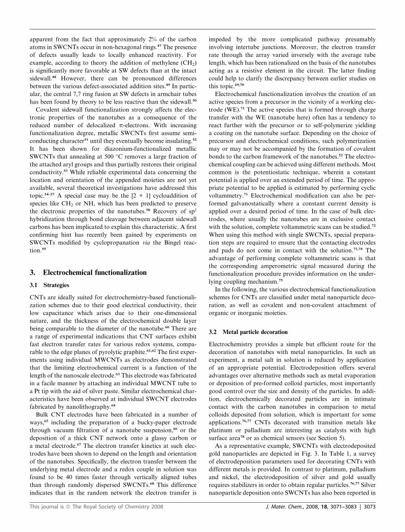
Fig. 2 Schematic depiction of a pentagon–heptagon pair (Stone–Wales
defect) in the sidewall of a carbon nanotube.
2.2 Chemical reactivity
The sites of highest chemical reactivity within carbon nanotubes
are the caps, which have a fullerene-like structure. Chemical
functionalization of CNT tips has been performed mainly on
the basis of oxidative treatments.18,19 As a general rule, CNT
purification by oxidation yields tubes with oxygen-containing
functional groups (predominantly carboxylic acid) at both the
sidewall and the tube endings. These groups can then be used
to link molecules via, e.g., amide bond formation.20
The curvature of the nanotube sidewall renders covalent bond
formation to the sp2 carbon framework more favorable than for
planar graphene.21 On this basis, a range of sidewall modification
protocols have been established, most notably involving the
addition of carbenes22,23 and azomethine ylides.24,25 Meanwhile,
there exist several experimental studies which reveal that the
(exohedral) chemical reactivity rises with increasing curvature
of the wall.26–28 This dependency has been attributed to curva-
ture-induced strain that originates from pyramidalization of
the sp2-hybridized carbon atoms and the misalignment of
p-orbitals.29–31 It is noteworthy that for certain types of nano-
tubes, the binding energy may increase instead of decrease
when going from smaller- to larger-diameter tubes. One example
is the chemisorption of hydrogen on zigzag tubes, as predicted by
a recent theoretical study.32 For a more comprehensive descrip-
tion, the direction dependence of curvature has to be taken
into account.33
3072 | J. Mater. Chem., 2008, 18, 3071–3083
Metallic and semiconducting SWCNTs display different
reactivity toward covalent functionalization, as has been demon-
strated for hydrogen peroxide-mediated oxidation,34 addition
reactions like the coupling of aromatic diazonium8 or nitronium9
ions, or osmylation.35 In general, m-SWCNTs, due to their larger
propensity for both donating and accepting electrons, exhibit
a higher reactivity than their semiconducting counterparts.36
However, it should be kept in mind that doping (as a result of,
e.g., the purification procedure) can render the reactivity of
semiconducting tubes comparable to that of the metallic
ones.37 This may explain experimental findings that the function-
alization is selective toward smaller diameter tubes, but largely
independent of the tubes’ electronic character.38
Like the chemisorption energy, the binding position of reac-
tive atoms or groups can depend on the type of nanotube. For
instance, while in case of armchair tubes pairs of hydrogen atoms
have been theoretically predicted to preferably attach to adjacent
positions,39,40 calculations on zigzag tubes indicate alternate
carbon sites to be most favorable.32 Interestingly, it has been
found that Clar’s valence bond model41 allows successful predic-
tion of the preferred pattern of covalently bonded hydrogen
atoms on CNTs.42
Defects such as vacancies and pentagon–heptagon pairs or
Stone–Wales (SW) defects (Fig. 2) profoundly alter the chemical
reactivity of the SWCNT sidewall.43–46 Their strong relevance is
This journal is ª The Royal Society of Chemistry 2008
apparent from the fact that approximately 2% of the carbon
atoms in SWCNTs occur in non-hexagonal rings.47 The presence
of defects usually leads to locally enhanced reactivity. For
example, according to theory the addition of methylene (CH2)
is significantly more favorable at SW defects than at the intact
sidewall.48 However, there can be pronounced differences
between the various defect-associated addition sites.49 In partic-
ular, the central 7,7 ring fusion at SW defects in armchair tubes
has been found by theory to be less reactive than the sidewall.50
Covalent sidewall functionalization strongly affects the elec-
tronic properties of the nanotubes as a consequence of the
reduced number of delocalized p-electrons. With increasing
functionalization degree, metallic SWCNTs first assume semi-
conducting character51 until they eventually become insulating.52
It has been shown for diazonium-functionalized metallic
SWCNTs that annealing at 500 �C removes a large fraction of
the attached aryl groups and thus partially restores their original
conductivity.53 While reliable experimental data concerning the
location and orientation of the appended moieties are not yet
available, several theoretical investigations have addressed this
topic.54–57 A special case may be the [2 + 1] cycloaddition of
species like CH2 or NH, which has been predicted to preserve
the electronic properties of the nanotubes.58 Recovery of sp2
hybridization through bond cleavage between adjacent sidewall
carbons has been implicated to explain this characteristic. A first
confirming hint has recently been gained by experiments on
SWCNTs modified by cyclopropanation via the Bingel reac-
tion.59
3. Electrochemical functionalization
3.1 Strategies
CNTs are ideally suited for electrochemistry-based functionali-
zation schemes due to their good electrical conductivity, their
low capacitance which arises due to their one-dimensional
nature, and the thickness of the electrochemical double layer
being comparable to the diameter of the nanotube.60 There are
a range of experimental indications that CNT surfaces exhibit
fast electron transfer rates for various redox systems, compa-
rable to the edge planes of pyrolytic graphite.61,62 The first exper-
iments using individual MWCNTs as electrodes demonstrated
that the limiting electrochemical current is a function of the
length of the nanoscale electrode.63 This electrode was fabricated
in a facile manner by attaching an individual MWCNT tube to
a Pt tip with the aid of silver paste. Similar electrochemical char-
acteristics have been observed at individual SWCNT electrodes
fabricated by nanolithography.64
Bulk CNT electrodes have been fabricated in a number of
ways,65 including the preparation of a bucky-paper electrode
through vacuum filtration of a nanotube suspension,66 or the
deposition of a thick CNT network onto a glassy carbon or
a metal electrode.67 The electron transfer kinetics at such elec-
trodes have been shown to depend on the length and orientation
of the nanotubes. Specifically, the electron transfer between the
underlying metal electrode and a redox couple in solution was
found to be 40 times faster through vertically aligned tubes
than through randomly dispersed SWCNTs.68 This difference
indicates that in the random network the electron transfer is
This journal is ª The Royal Society of Chemistry 2008
impeded by the more complicated pathway presumably
involving intertube junctions. Moreover, the electron transfer
rate through the array varied inversely with the average tube
length, which has been rationalized on the basis of the nanotubes
acting as a resistive element in the circuit. The latter finding
could help to clarify the discrepancy between earlier studies on
this topic.69,70
Electrochemical functionalization involves the creation of an
active species from a precursor in the vicinity of a working elec-
trode (WE).71 The active species that is formed through charge
transfer with the WE (nanotube here) often has a tendency to
react further with the precursor or to self-polymerize yielding
a coating on the nanotube surface. Depending on the choice of
precursor and electrochemical conditions, such polymerization
may or may not be accompanied by the formation of covalent
bonds to the carbon framework of the nanotubes.52 The electro-
chemical coupling can be achieved using different methods. Most
common is the potentiostatic technique, wherein a constant
potential is applied over an extended period of time. The appro-
priate potential to be applied is estimated by performing cyclic
voltammetry.71 Electrochemical modification can also be per-
formed galvanostatically where a constant current density is
applied over a desired period of time. In the case of bulk elec-
trodes, where usually the nanotubes are in exclusive contact
with the solution, complete voltammetric scans can be studied.72
When using this method with single SWCNTs, special prepara-
tion steps are required to ensure that the contacting electrodes
and pads do not come in contact with the solution.73,74 The
advantage of performing complete voltammetric scans is that
the corresponding amperometric signal measured during the
functionalization procedure provides information on the under-
lying coupling mechanism.75
In the following, the various electrochemical functionalization
schemes for CNTs are classified under metal nanoparticle deco-
ration, as well as covalent and non-covalent attachment of
organic or inorganic moieties.
3.2 Metal particle decoration
Electrochemistry provides a simple but efficient route for the
decoration of nanotubes with metal nanoparticles. In such an
experiment, a metal salt in solution is reduced by application
of an appropriate potential. Electrodeposition offers several
advantages over alternative methods such as metal evaporation
or deposition of pre-formed colloid particles, most importantly
good control over the size and density of the particles. In addi-
tion, electrochemically decorated particles are in intimate
contact with the carbon nanotubes in comparison to metal
colloids deposited from solution, which is important for some
applications.76,77 CNTs decorated with transition metals like
platinum or palladium are interesting as catalysts with high
surface area78 or as chemical sensors (see Section 5).
As a representative example, SWCNTs with electrodeposited
gold nanoparticles are depicted in Fig. 3. In Table 1, a survey
of electrodeposition parameters used for decorating CNTs with
different metals is provided. In contrast to platinum, palladium
and nickel, the electrodeposition of silver and gold usually
requires stabilizers in order to obtain regular particles.76,77 Silver
nanoparticle deposition onto SWCNTs has also been reported in
J. Mater. Chem., 2008, 18, 3071–3083 | 3073
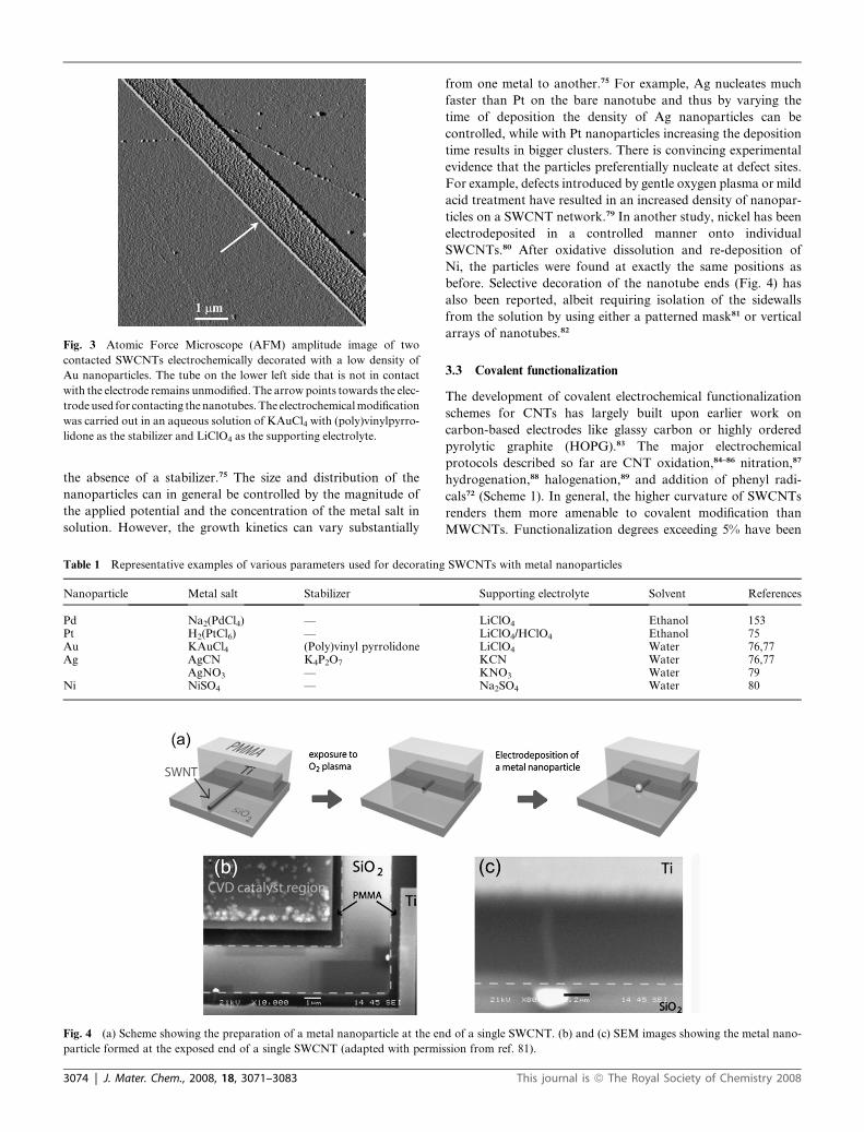
Fig. 3 Atomic Force Microscope (AFM) amplitude image of two
contacted SWCNTs electrochemically decorated with a low density of
Au nanoparticles. The tube on the lower left side that is not in contact
with the electrode remains unmodified. The arrow points towards the elec-
trodeused for contacting the nanotubes.The electrochemicalmodification
was carried out in an aqueous solution of KAuCl4 with (poly)vinylpyrro-
lidone as the stabilizer and LiClO4 as the supporting electrolyte.
the absence of a stabilizer.75 The size and distribution of the
nanoparticles can in general be controlled by the magnitude of
the applied potential and the concentration of the metal salt in
solution. However, the growth kinetics can vary substantially
Table 1 Representative examples of various parameters used for decorating
Nanoparticle Metal salt Stabilizer
Pd Na2(PdCl4) —Pt H2(PtCl6) —Au KAuCl4 (Poly)vinyl pyrrolidoneAg AgCN K4P2O7
AgNO3 —Ni NiSO4 —
Fig. 4 (a) Scheme showing the preparation of a metal nanoparticle at the en
particle formed at the exposed end of a single SWCNT (adapted with permi
3074 | J. Mater. Chem., 2008, 18, 3071–3083
from one metal to another.75 For example, Ag nucleates much
faster than Pt on the bare nanotube and thus by varying the
time of deposition the density of Ag nanoparticles can be
controlled, while with Pt nanoparticles increasing the deposition
time results in bigger clusters. There is convincing experimental
evidence that the particles preferentially nucleate at defect sites.
For example, defects introduced by gentle oxygen plasma or mild
acid treatment have resulted in an increased density of nanopar-
ticles on a SWCNT network.79 In another study, nickel has been
electrodeposited in a controlled manner onto individual
SWCNTs.80 After oxidative dissolution and re-deposition of
Ni, the particles were found at exactly the same positions as
before. Selective decoration of the nanotube ends (Fig. 4) has
also been reported, albeit requiring isolation of the sidewalls
from the solution by using either a patterned mask81 or vertical
arrays of nanotubes.82
3.3 Covalent functionalization
The development of covalent electrochemical functionalization
schemes for CNTs has largely built upon earlier work on
carbon-based electrodes like glassy carbon or highly ordered
pyrolytic graphite (HOPG).83 The major electrochemical
protocols described so far are CNT oxidation,84–86 nitration,87
hydrogenation,88 halogenation,89 and addition of phenyl radi-
cals72 (Scheme 1). In general, the higher curvature of SWCNTs
renders them more amenable to covalent modification than
MWCNTs. Functionalization degrees exceeding 5% have been
SWCNTs with metal nanoparticles
Supporting electrolyte Solvent References
LiClO4 Ethanol 153LiClO4/HClO4 Ethanol 75LiClO4 Water 76,77KCN Water 76,77KNO3 Water 79Na2SO4 Water 80
d of a single SWCNT. (b) and (c) SEM images showing the metal nano-
ssion from ref. 81).
This journal is ª The Royal Society of Chemistry 2008
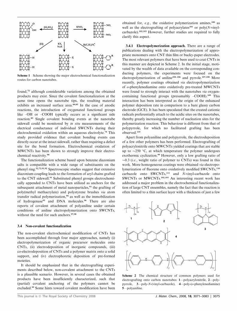
Scheme 1 Scheme showing the major electrochemical functionalization
routes for carbon nanotubes.
found,72 although considerable variations among the obtained
products may exist. Since the covalent functionalization at the
same time opens the nanotube tips, the resulting material
exhibits an increased surface area.84,85 In the case of anodic
reactions, the introduction of oxygenated functional groups
like –OH or –COOH typically occurs as a significant side
reaction.89 Single covalent bonding events at the nanotube
sidewall could be monitored by in situ measurements of the
electrical conductance of individual SWCNTs during their
electrochemical oxidation within an aqueous electrolyte.74 This
study provided evidence that covalent bonding events can
directly occur at the intact sidewall, rather than requiring a defect
site for the bond formation. Electrochemical oxidation of
MWCNTs has been shown to strongly improve their electro-
chemical reactivity.90
The functionalization scheme based upon benzene diazonium
salts is compatible with a wide range of substituents on the
phenyl ring.52,72,91,92 Spectroscopic studies suggest that extensive
diazonium coupling leads to the formation of aryl chains grafted
to the CNT sidewall.91 Substituted phenyl groups electrochemi-
cally appended to CNTs have been utilized as anchors for the
subsequent attachment of metal nanoparticles,93 the grafting of
poly(methyl methacrylate) and polystyrene brushes via atom
transfer radical polymerization,94 as well as the immobilization
of hydrogenase95 and DNA molecules.96 There are also
reports of covalent attachment of polyaniline under certain
conditions of aniline electropolymerization onto SWCNTs,
without the need for such anchors.97,98
Scheme 2 The chemical structure of common polymers used for
electrografting onto carbon nanotubes: 1—polyacrylonitrile, 2—poly-
pyrrole, 3—poly-N-(vinyl-carbazole), 4—poly-(o-phenylenediamine)
5—polyaniline.
3.4 Non-covalent functionalization
The non-covalent electrochemical modification of CNTs has
been accomplished through four major approaches, namely (i)
electropolymerization of organic precursor molecules onto
CNTs, (ii) electrodeposition of inorganic compounds, (iii)
co-electrodeposition of CNTs and a polymer matrix onto a solid
support, and (iv) electrophoretic deposition of pre-formed
moieties.
It should be emphasized that in the electrografting experi-
ments described below, non-covalent attachment to the CNTs
is a plausible scenario. However, in several cases the obtained
products have been insufficiently characterized, such that
(partial) covalent anchoring of the polymers cannot be
excluded.99 Some hints toward covalent modification have been
This journal is ª The Royal Society of Chemistry 2008
obtained for, e.g., the oxidative polymerization amines,100 as
well as the electrografting of polyacrylates101 or poly(N-vinyl-
carbazole).102,103 However, further studies are required to fully
clarify this aspect.
3.4.1 Electropolymerization approach. There are a range of
publications dealing with the electropolymerization of appro-
priate monomers onto CNT thin film or bucky-paper electrodes.
The most relevant polymers that have been used to coat CNTs in
this manner are depicted in Scheme 2. In the initial stage, moti-
vated by the wealth of data available on the corresponding con-
ducting polymers, the experiments were focused on the
electropolymerization of aniline104–106 and pyrrole.107,108 More
recently, polymer coatings obtained via electropolymerization
of o-phenylenediamine onto oxidatively pre-treated MWCNTs
were found to strongly interact with the nanotubes via oxygen-
containing functional groups (presumably –COOH).109 This
interaction has been interpreted as the origin of the enhanced
polymer deposition rate in comparison to a bare glassy carbon
electrode (GCE). It has been speculated that the created cationic
radicals preferentially attach to the acidic sites on the nanotubes,
thereby greatly increasing the number of nucleation sites for the
polymerization reaction. This behaviour is different from that of
polypyrrole, for which no facilitated grafting has been
observed.110
Apart from polyaniline and polypyrrole, the electrodeposition
of a few other polymers has been performed. Electrografting of
polyacrylonitrile onto MWCNTs yielded coatings that are stable
up to �250 �C, at which temperature the polymer undergoes
exothermic cyclization.99 However, only a low grafting ratio of
�0.3 (i.e., weight ratio of polymer to CNTs) was found in this
work. More homogeneous coatings were obtained via electropo-
lymerization of fluorene onto oxidatively modified SWCNTs,110
carbazole onto SWCNTs,111 and N-vinyl-carbazole onto
SWCNTs or MWCNTs.102,103 An interesting recent work has
addressed a major problem in the electrochemical functionaliza-
tion of large CNT ensembles, namely the fact that the reaction is
often limited to a thin surface layer with a thickness of just a few
J. Mater. Chem., 2008, 18, 3071–3083 | 3075
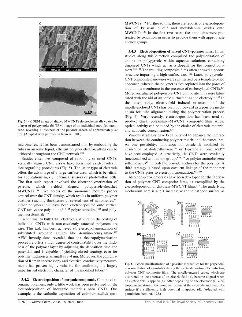
Fig. 6 Schematic illustration of a possible mechanism for the perpendic-
ular orientation of nanotubes during the electrodeposition of conducting
polymer–CNT composite films. The micelle-encased tubes, which are
disordered in the absence of an electric field (a), become aligned when
an electric field is applied (b). After depositing on the electrode (c), elec-
tropolymerization of the monomer occurs at the electrode and nanotube
surface if a sufficiently high potential is applied (d). (Adapted with
permission from ref. 125.)
Fig. 5 (a) SEM image of aligned MWCNTs electrochemically coated by
a layer of polypyrrole; (b) TEM image of an individual modified nano-
tube, revealing a thickness of the polymer sheath of approximately 30
nm. (Adapted with permission from ref. 201.)
micrometres. It has been demonstrated that by embedding the
tubes in an ionic liquid, efficient polymer electrografting can be
achieved throughout the CNT network.101
Besides ensembles composed of randomly oriented CNTs,
vertically aligned CNT arrays have been used as electrodes in
electrografting procedures (Fig. 5). The latter type of electrode
offers the advantage of a large surface area, which is beneficial
for applications in, e.g., chemical sensors or photovoltaic cells.
The first such report involved the electropolymerization of
pyrrole, which yielded aligned polypyrrole-sheathed
MWCNTs.104 Free access of the monomer requires proper
control over the CNT density, which results in uniform polymer
coatings reaching thicknesses of several tens of nanometres.112
Other polymers that have been electrodeposited onto vertical
CNT arrays are polyaniline,113,114 poly(o-anisidine)115 and poly-
methacrylonitrile.116
In contrast to bulk CNT electrodes, studies on the coating of
individual CNTs with non-covalently attached polymers are
rare. This task has been achieved via electropolymerization of
substituted aromatic amines like 4-amino-benzylamine.117
AFM investigations revealed that the electropolymerization
procedure offers a high degree of controllability over the thick-
ness of the polymer layer by adjusting the deposition time and
potential, and is capable of yielding closed coatings even for
polymer thicknesses as small as 3–4 nm. Moreover, the combina-
tion of Raman spectroscopy and electrical conductivity measure-
ments has proven highly valuable for confirming the largely
unperturbed electronic character of the modified tubes.52
3.4.2 Electrodeposition of inorganic compounds. Compared to
organic polymers, only a little work has been performed on the
electrodeposition of inorganic materials onto CNTs. One
example is the cathodic deposition of cadmium sulfide onto
3076 | J. Mater. Chem., 2008, 18, 3071–3083
MWCNTs.118 Further to this, there are reports of electrodeposi-
tion of Prussian blue119 and molybdenum oxides onto
MWCNTs.120 In the first two cases, the nanotubes were pre-
treated by oxidation in order to provide them with appropriate
anchor groups.
3.4.3 Electrodeposition of mixed CNT–polymer films. Initial
studies along this direction comprised the polymerization of
aniline or polypyrrole within aqueous solutions containing
dispersed CNTs which act as a dopant for the formed poly-
mers.121,122 The resulting composite films often showed a porous
structure imparting a high surface area.123 Later, polypyrrole–
CNT composite nanowires were synthesized by a template-based
approach, wherein the polymer is electroplated into the pores of
an alumina membrane in the presence of carboxylated CNTs.124
Moreover, aligned polypyrrole–CNT composite films were fabri-
cated with the aid of an ionic surfactant as the electrolyte.125 In
the latter study, electric-field induced orientation of the
micelle-enclosed CNTs has been put forward as a possible mech-
anism for tube alignment during the polymerization process
(Fig. 6). Very recently, electrodeposition has been used to
produce chiral polyaniline–MWCNT composite films whose
optical activity can be tuned by the choice of electrode material
and nanotube concentration.126
Various strategies have been pursued to enhance the interac-
tion between the conducting polymer matrix and the nanotubes.
As one possibility, nanotubes non-covalently modified by
adsorption of dodecylbenzene127 or 1-pyrene sulfonic acid128
have been employed. Alternatively, the CNTs were covalently
functionalized with amino groups129,130 or poly(m-aminobenzene
sulfonic acid)131 in order to provide anchors for the polymer. A
third strategy is based upon covalent linkage of the monomer
to the CNTs prior to electropolymerization.132–136
Also non-redox processes have been developed for the fabrica-
tion of polymer–CNT composite films, as exemplified by the
electrodeposition of chitosan–MWCNT films.137 The underlying
mechanism here is a pH increase near the cathode surface as
This journal is ª The Royal Society of Chemistry 2008
a consequence of proton reduction, which causes precipitation of
the chitosan.
3.4.4 Electrophoretic deposition. Electrophoretic coating, an
approach that has received the smallest attention so far, has
been used to deposit protonated, positively charged titanium
dioxide clusters in high density along vertically aligned
MWCNTs.138 The thickness of the resulting homogeneous
TiO2 coatings could be controlled by the applied voltage and
deposition time.
4. Field-effect transistors
Amajor impetus for increasing research in the field of CNTs was
the fabrication of field-effect transistors (FETs).3,4 In fact, the
realization of transistors with just a nanometre-wide channel
was expected to further stimulate the miniaturization drive in
information technologies. However, this expectation has not
yet been fulfilled, which is largely due to the fact that CNTs—
unlike conventional semiconductor materials—are available
mostly as a mixture of m- and s-SWCNTs. Hence, for routine
fabrication of CNT-FETs, the m-SWCNTs need to be elimi-
nated either before or after their implementation into a device.
Within the first approach, different chemical methods have
been used which exploit for instance the differing interaction
between m- and s-SWCNTs with various polymers,15 although
the attained enrichment factors are still well below 100%.
More promising separation efficiencies have been attained by
physical methods like dielectrophoresis139 and density gradient
centrifugation,140 however, it is more difficult to scale-up these
procedures.
The most common technique employed for eliminating
m-SWCNTs at the device level involves destruction of the
m-SWCNTs by passing a high current through the CNT
ensemble.141 Here a back-gate is required in order to switch the
s-SWCNTs to the OFF state, in order to ensure that the current
is exclusively carried by the metallic tubes. Another selective
elimination method applicable to CNT devices is electrochemical
functionalization, which has been demonstrated in two different
ways. In the first variant, the hysteresis of back-gated SWCNT-
FETs is utilized to bring the s-SWCNTs within a network to the
OFF state by sweeping the back-gate voltage appropriately.142
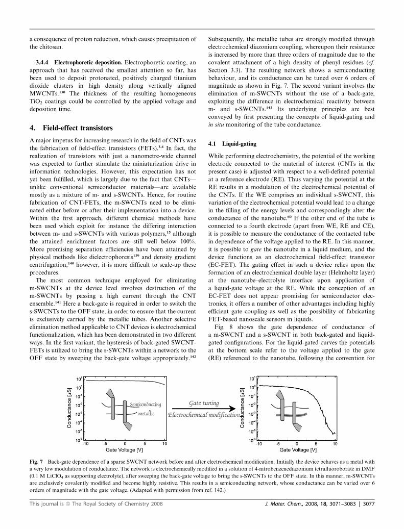
Fig. 7 Back-gate dependence of a sparse SWCNT network before and after
a very low modulation of conductance. The network is electrochemically mod
(0.1 M LiClO4 as supporting electrolyte), after sweeping the back-gate voltag
are exclusively covalently modified and become highly resistive. This results
orders of magnitude with the gate voltage. (Adapted with permission from r
This journal is ª The Royal Society of Chemistry 2008
Subsequently, the metallic tubes are strongly modified through
electrochemical diazonium coupling, whereupon their resistance
is increased by more than three orders of magnitude due to the
covalent attachment of a high density of phenyl residues (cf.
Section 3.3). The resulting network shows a semiconducting
behaviour, and its conductance can be tuned over 6 orders of
magnitude as shown in Fig. 7. The second variant involves the
elimination of m-SWCNTs without the use of a back-gate,
exploiting the difference in electrochemical reactivity between
m- and s-SWCNTs.143 Its underlying principles are best
conveyed by first presenting the concepts of liquid-gating and
in situ monitoring of the tube conductance.
4.1 Liquid-gating
While performing electrochemistry, the potential of the working
electrode connected to the material of interest (CNTs in the
present case) is adjusted with respect to a well-defined potential
at a reference electrode (RE). Thus varying the potential at the
RE results in a modulation of the electrochemical potential of
the CNTs. If the WE comprises an individual s-SWCNT, this
variation of the electrochemical potential would lead to a change
in the filling of the energy levels and correspondingly alter the
conductance of the nanotube.60 If the other end of the tube is
connected to a fourth electrode (apart from WE, RE and CE),
it is possible to measure the conductance of the contacted tube
in dependence of the voltage applied to the RE. In this manner,
it is possible to gate the nanotube in a liquid medium, and the
device functions as an electrochemical field-effect transistor
(EC-FET). The gating effect in such a device relies upon the
formation of an electrochemical double layer (Helmholtz layer)
at the nanotube–electrolyte interface upon application of
a liquid-gate voltage at the RE. While the conception of an
EC-FET does not appear promising for semiconductor elec-
tronics, it offers a number of other advantages including highly
efficient gate coupling as well as the possibility of fabricating
FET-based nanoscale sensors in liquids.
Fig. 8 shows the gate dependence of conductance of
a m-SWCNT and a s-SWCNT in both back-gated and liquid-
gated configurations. For the liquid-gated curves the potentials
at the bottom scale refer to the voltage applied to the gate
(RE) referenced to the nanotube, following the convention for
electrochemical modification. Initially the device behaves as a metal with
ified in a solution of 4-nitrobenzenediazonium tetrafluoroborate in DMF
e to bring the s-SWCNTs to the OFF state. In this manner, m-SWCNTs
in a semiconducting network, whose conductance can be varied over 6
ef. 142.)
J. Mater. Chem., 2008, 18, 3071–3083 | 3077
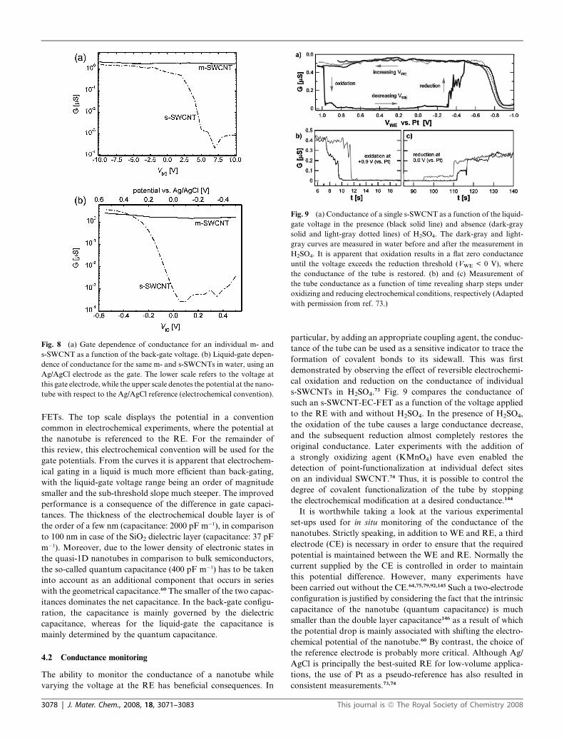
Fig. 8 (a) Gate dependence of conductance for an individual m- and
s-SWCNT as a function of the back-gate voltage. (b) Liquid-gate depen-
dence of conductance for the same m- and s-SWCNTs in water, using an
Ag/AgCl electrode as the gate. The lower scale refers to the voltage at
this gate electrode, while the upper scale denotes the potential at the nano-
tube with respect to the Ag/AgCl reference (electrochemical convention).
Fig. 9 (a) Conductance of a single s-SWCNT as a function of the liquid-
gate voltage in the presence (black solid line) and absence (dark-gray
solid and light-gray dotted lines) of H2SO4. The dark-gray and light-
gray curves are measured in water before and after the measurement in
H2SO4. It is apparent that oxidation results in a flat zero conductance
until the voltage exceeds the reduction threshold (VWE < 0 V), where
the conductance of the tube is restored. (b) and (c) Measurement of
the tube conductance as a function of time revealing sharp steps under
oxidizing and reducing electrochemical conditions, respectively (Adapted
with permission from ref. 73.)
FETs. The top scale displays the potential in a convention
common in electrochemical experiments, where the potential at
the nanotube is referenced to the RE. For the remainder of
this review, this electrochemical convention will be used for the
gate potentials. From the curves it is apparent that electrochem-
ical gating in a liquid is much more efficient than back-gating,
with the liquid-gate voltage range being an order of magnitude
smaller and the sub-threshold slope much steeper. The improved
performance is a consequence of the difference in gate capaci-
tances. The thickness of the electrochemical double layer is of
the order of a few nm (capacitance: 2000 pF m�1), in comparison
to 100 nm in case of the SiO2 dielectric layer (capacitance: 37 pF
m�1). Moreover, due to the lower density of electronic states in
the quasi-1D nanotubes in comparison to bulk semiconductors,
the so-called quantum capacitance (400 pF m�1) has to be taken
into account as an additional component that occurs in series
with the geometrical capacitance.60 The smaller of the two capac-
itances dominates the net capacitance. In the back-gate configu-
ration, the capacitance is mainly governed by the dielectric
capacitance, whereas for the liquid-gate the capacitance is
mainly determined by the quantum capacitance.
4.2 Conductance monitoring
The ability to monitor the conductance of a nanotube while
varying the voltage at the RE has beneficial consequences. In
3078 | J. Mater. Chem., 2008, 18, 3071–3083
particular, by adding an appropriate coupling agent, the conduc-
tance of the tube can be used as a sensitive indicator to trace the
formation of covalent bonds to its sidewall. This was first
demonstrated by observing the effect of reversible electrochemi-
cal oxidation and reduction on the conductance of individual
s-SWCNTs in H2SO4.73 Fig. 9 compares the conductance of
such an s-SWCNT-EC-FET as a function of the voltage applied
to the RE with and without H2SO4. In the presence of H2SO4,
the oxidation of the tube causes a large conductance decrease,
and the subsequent reduction almost completely restores the
original conductance. Later experiments with the addition of
a strongly oxidizing agent (KMnO4) have even enabled the
detection of point-functionalization at individual defect sites
on an individual SWCNT.74 Thus, it is possible to control the
degree of covalent functionalization of the tube by stopping
the electrochemical modification at a desired conductance.144
It is worthwhile taking a look at the various experimental
set-ups used for in situ monitoring of the conductance of the
nanotubes. Strictly speaking, in addition to WE and RE, a third
electrode (CE) is necessary in order to ensure that the required
potential is maintained between the WE and RE. Normally the
current supplied by the CE is controlled in order to maintain
this potential difference. However, many experiments have
been carried out without the CE.64,75,79,92,145 Such a two-electrode
configuration is justified by considering the fact that the intrinsic
capacitance of the nanotube (quantum capacitance) is much
smaller than the double layer capacitance146 as a result of which
the potential drop is mainly associated with shifting the electro-
chemical potential of the nanotube.60 By contrast, the choice of
the reference electrode is probably more critical. Although Ag/
AgCl is principally the best-suited RE for low-volume applica-
tions, the use of Pt as a pseudo-reference has also resulted in
consistent measurements.73,74
This journal is ª The Royal Society of Chemistry 2008
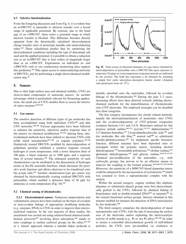
Fig. 10 Time course of electrical resistance of a gas sensor obtained by
electrodeposition of polyaniline onto a SWCNT film upon exposure to
ammonia (10 ppm) at room temperature (exposure periods are indicated
be the arrows). The bold line represents a fit obtained by assuming
a simple first order adsorption–desorption kinetic model. (Adapted
with permission from ref. 157.)
4.3 Selective functionalization
From the foregoing discussion and from Fig. 8, it is evident that
an m-SWCNT is amenable to electron transfer over a broad
range of applicable potentials. By contrast, due to the band
gap of an s-SWCNT, there exists a potential range in which
electron transfer is blocked. This difference becomes directly
apparent from the theoretically calculated electrochemical
charge transfer rates of prototype metallic and semiconducting
tubes.143 These calculations predict that by optimizing the
electrochemical conditions including the type of diazonium salt
used and the applied potential, it is possible to obtain a reduction
rate at an m-SWCNT that is four orders of magnitude larger
than at an s-SWCNT. Experiments on individual m- and
s-SWCNTs with in situ conductance monitoring data support
this prediction.143 This opens access to semiconducting networks
of SWCNTs, just by performing a single electrochemical modifi-
cation step.10
5. Sensors
Due to their high surface area and chemical stability, CNTs are
close-to-ideal components of nanoscale sensors. As another
advantage, which is particularly relevant for biosensing applica-
tions, the small size of CNTs enables them to access the interior
of redox enzymes.69,70,147
5.1 Gas sensors
The sensitive detection of different types of gas molecules has
been accomplished using both individual CNTs148 and thin
CNT networks.149,150 Various approaches have been followed
to enhance the sensitivity, selectivity and/or response time of
the sensors via chemical modification.151,152 Among these, elec-
trochemical methods have been utilized to decorate CNTs with
noble metal nanoparticles153–156 or organic polymers.157,158
Oxidatively treated SWCNTs modified by electrodeposition of
palladium particles exhibited a sensitive response towards
hydrogen at room temperature, with a lower detection limit of
100 ppm, a linear response up to 1000 ppm, and a response
time of several minutes.154 The enhanced sensitivity of such
chemiresistors can be attributed to the dissociation of hydrogen
atoms at the Pd–nanotube interface, which decreases the parti-
cle’s work function and allows electrons to be transferred onto
the p-type tube.153 Another chemiresistor-type gas sensor was
obtained by electrochemically coating oxidized SWCNTs with
polyaniline, which enabled a detection limit of 50 ppb for
ammonia at room temperature (Fig. 10).157
5.2 Chemical sensing of (bio)molecules
5.2.1 Electrochemical sensors. Numerous amperometric and
voltammetric sensors have been realized on the basis of covalent
or non-covalent linkage of appropriate modifying molecules
(e.g., enzymes, DNA) to CNTs in order to improve their electro-
analytical response. In the vast majority of these studies, the
attachment was carried out using solution-based chemical modi-
fication protocols159 involving direct adsorption,160 amide or
ester couplings to surface carboxyl groups on the tubes,161–163
or a ‘mixed’ approach wherein a suitable linker molecule is
This journal is ª The Royal Society of Chemistry 2008
initially adsorbed onto the nanotubes, followed by covalent
linkage of the (bio)molecules.164 During the past 2–3 years,
increasing efforts have been directed towards utilizing electro-
chemical methods for the immobilization of (bio)molecules
onto CNT electrodes. The employed strategies can be classified
into three categories.
The first category encompasses two closely related methods,
namely the electropolymerization of monomers onto CNTs
and the co-electrodeposition of CNT–polymer composites
(compare Sections 3.4.1 and 3.4.3). Monomers utilized for this
purpose include aniline,165–171 pyrrole,172–175 diphenylamine,176
3,30-diamino-benzidine,177 2,6-pyridinedicarboxylic acid,178 and
dye molecules like nile blue,179 neutral red180 or substituted
metallo-phthalocyanines.181 To implement specific biosensor
function, different enzymes have been deposited onto or
entrapped within the polymer matrix, including alcohol
dehydrogenase,179 horseradish polymerase,170 choline oxidase,167
glutamate dehydrogenase,174 and glucose oxidase.165,172,173,177
Chemical pre-modification of the nanotubes, e.g., with
carboxylic groups, has proven to be an effective means to
improve the coupling to the formed polymer.166,168,172–176,178,180
Moreover, the sensitivity of a MWCNT-based dopamine sensor
could be enhanced by the incorporation of cyclodextrin,169 which
was assumed to form a supramolecular complex with the
analyte.
Within the second category, organic residues like aliphatic
diamines or substituted phenyl groups were first electrochemi-
cally grafted to the CNTs, followed by chemical linking of
biopolymers such as double-stranded DNA182 or enzymes183 to
the created functional surface groups. Sensors obtained in this
manner enabled for instance the detection of DNA intercalation
by dye molecules.182
The third category comprises the electrodeposition of metal
nanoparticles onto CNTs, with the aim of increasing the surface
area of the electrodes and/or exploiting the electrocatalytic
activity of noble metals (e.g., Pt or Au–Pt alloy).184–186 In order
to ensure a controlled electrochemical growth of well-defined
particles, the CNTs were pre-modified via oxidation or
J. Mater. Chem., 2008, 18, 3071–3083 | 3079
adsorption of charged polyelectrolytes. Glucose sensors could
then be realized through direct or indirect attachment of glucose
oxidase to the metal particles.
5.2.2 Chemiresistors. Chemiresistors are devices whose
resistance is directly proportional to the chemical or biological
input (analyte concentration). Their active components are
most commonly metal oxides used for gas sensing,187 albeit
chemiresistors for application in liquid phase gain increasing
importance. One example is a composite polymer chemiresistor,
where analytes cause swelling and in turn an increase in resis-
tance.188 CNTs are suitable dopants for such polymer matrices,
as exemplified by the fabrication of a micro-gap chemiresistor
with MWCNTs incorporated into electropolymerized polypyr-
role.189 This sensor exhibited a linear response to H2O2 and
could be extended to detect glucose by incorporating glucose
oxidase. In general, while chemiresistors are advantageous
because they do not require a reference electrode or electron
mediators, they suffer from problems such as the need for
frequent calibration.
CNTs are excellently suited for the miniaturization of
chemiresistors. Since the device resistance is a key-factor in
such devices, m-SWCNTs are normally chosen due to their
higher conductance (in comparison to their semiconducting
counterparts), which remains fairly constant as a function of
gate-voltage. For sensor implementation, analyte-sensitive
functional groups need to be coupled onto the surface of the
m-SWCNTs. Furthermore, the functionalization degree needs
to be controllable so that the tube is not completely destroyed.52
All these requirements are granted by the electrochemical
covalent modification method with the in situ conductance
monitoring capability,144 as demonstrated by the fabrication of
a pH sensor through controlled covalent attachment of diethyla-
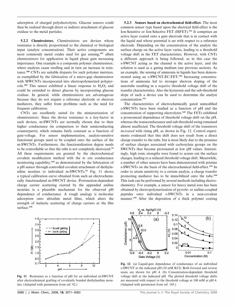
niline moeities to individual m-SWCNTs.92 Fig. 11 shows
a typical calibration curve obtained from such an electrochemi-
cally functionalized m-SWCNT device. Protonation-dependent
charge carrier scattering exerted by the appended aniline
moieties is a plausible mechanism for the observed pH
dependence of conductance. A rough analogy is molecular
adsorption onto ultrathin metal films, which alters the
strength of inelastic scattering of charge carriers at the film
surface.190
Fig. 11 Resistance as a function of pH for an individual m-SWCNT
after electrochemical grafting of covalently bonded diethylaniline moie-
ties. (Adapted with permission from ref. 92.)
3080 | J. Mater. Chem., 2008, 18, 3071–3083
5.2.3 Sensors based on electrochemical field-effect. The most
common sensor type based upon the electrical field-effect is the
Ion-Sensitive or Ion-Selective FET (ISFET).191 It comprises an
active layer coated onto a gate electrode that is in contact with
the liquid and whose potential is set with respect to a reference
electrode. Depending on the concentration of the analyte the
surface charge on the active layer varies, leading to a threshold
voltage shift in the FET characteristics. However, with CNTs
a different approach is being followed, as in this case the
s-SWCNT acting as the channel is the active layer, and the
solution is used as a gating medium (see previous section). As
an example, the sensing of ammonia in liquids has been demon-
strated using an s-SWCNT-EC-FET.192 Increasing concentra-
tions of ammonia led to stronger electron doping of the
nanotube resulting in a negative threshold voltage shift of the
transfer characteristics. Also the hysteresis and the sub-threshold
slope of such a device can be used to determine the analyte
concentration.193
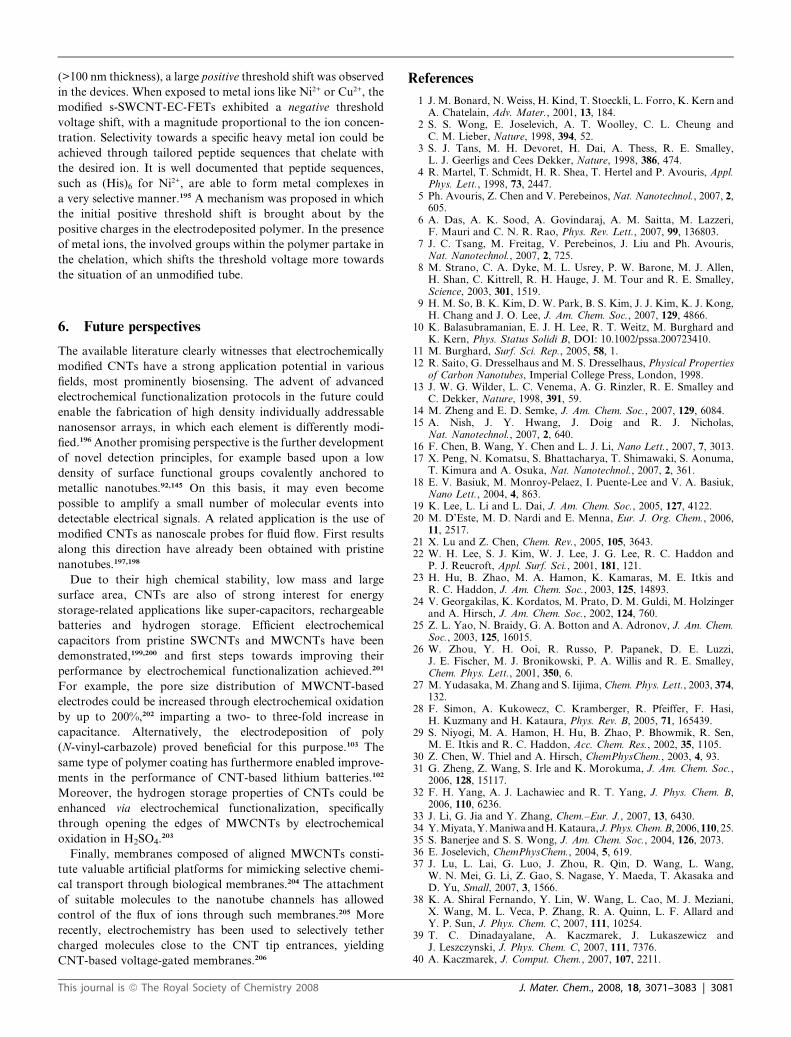
The characteristics of electrochemically gated unmodified
s-SWCNTs have been studied as a function of pH and the
concentration of supporting electrolytes.145 The FETs exhibited
a pronounced dependence of threshold voltage shift on the pH,
whereas the transconductance and sub-threshold swing remained
almost unaffected. The threshold voltage shift of the transistors
increased with rising pH, as shown in Fig. 12. Control experi-
ments evidenced that this shift does not result from a direct
charge transfer to the tube, but is most likely due to the presence
of surface charges associated with carboxylate groups on the
SWCNTs that become protonated at low pH values. Interest-
ingly, high ionic strengths were found to screen out the surface
charges, leading to a reduced threshold voltage shift. Meanwhile,
a number of other sensors have been demonstrated with pristine
s-SWCNTs on the basis of the electrochemical field-effect.193 In
order to attain sensitivity to a certain analyte, a charge transfer
promoting mediator has to be immobilized onto the tube.194
This task can be performed by several methods including electro-
chemistry. For example, a sensor for heavy metal ions has been
obtained by electropolymerization of pyrrole- or aniline-coupled
peptides onto individual s-SWCNTs in a non-covalent
manner.195 After the deposition of a thick polymer coating
Fig. 12 (a) Liquid-gate dependence of conductance of an individual
s-SWCNT at the indicated pH (10 mM KCl). Both forward and reverse
scans are shown for pH 4. (b) Concentration-dependent threshold
voltage shift at the indicated pH. The plotted threshold voltage shifts
are measured with respect to the threshold voltage at 100 mM at pH 4.
(Adapted with permission from ref. 145.)
This journal is ª The Royal Society of Chemistry 2008
(>100 nm thickness), a large positive threshold shift was observed
in the devices. When exposed to metal ions like Ni2+ or Cu2+, the
modified s-SWCNT-EC-FETs exhibited a negative threshold
voltage shift, with a magnitude proportional to the ion concen-
tration. Selectivity towards a specific heavy metal ion could be
achieved through tailored peptide sequences that chelate with
the desired ion. It is well documented that peptide sequences,
such as (His)6 for Ni2+, are able to form metal complexes in
a very selective manner.195 A mechanism was proposed in which
the initial positive threshold shift is brought about by the
positive charges in the electrodeposited polymer. In the presence
of metal ions, the involved groups within the polymer partake in
the chelation, which shifts the threshold voltage more towards
the situation of an unmodified tube.
6. Future perspectives
The available literature clearly witnesses that electrochemically
modified CNTs have a strong application potential in various
fields, most prominently biosensing. The advent of advanced
electrochemical functionalization protocols in the future could
enable the fabrication of high density individually addressable
nanosensor arrays, in which each element is differently modi-
fied.196 Another promising perspective is the further development
of novel detection principles, for example based upon a low
density of surface functional groups covalently anchored to
metallic nanotubes.92,145 On this basis, it may even become
possible to amplify a small number of molecular events into
detectable electrical signals. A related application is the use of
modified CNTs as nanoscale probes for fluid flow. First results
along this direction have already been obtained with pristine
nanotubes.197,198
Due to their high chemical stability, low mass and large
surface area, CNTs are also of strong interest for energy
storage-related applications like super-capacitors, rechargeable
batteries and hydrogen storage. Efficient electrochemical
capacitors from pristine SWCNTs and MWCNTs have been
demonstrated,199,200 and first steps towards improving their
performance by electrochemical functionalization achieved.201
For example, the pore size distribution of MWCNT-based
electrodes could be increased through electrochemical oxidation
by up to 200%,202 imparting a two- to three-fold increase in
capacitance. Alternatively, the electrodeposition of poly
(N-vinyl-carbazole) proved beneficial for this purpose.103 The
same type of polymer coating has furthermore enabled improve-
ments in the performance of CNT-based lithium batteries.102
Moreover, the hydrogen storage properties of CNTs could be
enhanced via electrochemical functionalization, specifically
through opening the edges of MWCNTs by electrochemical
oxidation in H2SO4.203
Finally, membranes composed of aligned MWCNTs consti-
tute valuable artificial platforms for mimicking selective chemi-
cal transport through biological membranes.204 The attachment
of suitable molecules to the nanotube channels has allowed
control of the flux of ions through such membranes.205 More
recently, electrochemistry has been used to selectively tether
charged molecules close to the CNT tip entrances, yielding
CNT-based voltage-gated membranes.206
This journal is ª The Royal Society of Chemistry 2008
References
1 J. M. Bonard, N.Weiss, H. Kind, T. Stoeckli, L. Forro, K. Kern andA. Chatelain, Adv. Mater., 2001, 13, 184.
2 S. S. Wong, E. Joselevich, A. T. Woolley, C. L. Cheung andC. M. Lieber, Nature, 1998, 394, 52.
3 S. J. Tans, M. H. Devoret, H. Dai, A. Thess, R. E. Smalley,L. J. Geerligs and Cees Dekker, Nature, 1998, 386, 474.
4 R. Martel, T. Schmidt, H. R. Shea, T. Hertel and P. Avouris, Appl.Phys. Lett., 1998, 73, 2447.
5 Ph. Avouris, Z. Chen and V. Perebeinos, Nat. Nanotechnol., 2007, 2,605.
6 A. Das, A. K. Sood, A. Govindaraj, A. M. Saitta, M. Lazzeri,F. Mauri and C. N. R. Rao, Phys. Rev. Lett., 2007, 99, 136803.
7 J. C. Tsang, M. Freitag, V. Perebeinos, J. Liu and Ph. Avouris,Nat. Nanotechnol., 2007, 2, 725.
8 M. Strano, C. A. Dyke, M. L. Usrey, P. W. Barone, M. J. Allen,H. Shan, C. Kittrell, R. H. Hauge, J. M. Tour and R. E. Smalley,Science, 2003, 301, 1519.
9 H. M. So, B. K. Kim, D. W. Park, B. S. Kim, J. J. Kim, K. J. Kong,H. Chang and J. O. Lee, J. Am. Chem. Soc., 2007, 129, 4866.
10 K. Balasubramanian, E. J. H. Lee, R. T. Weitz, M. Burghard andK. Kern, Phys. Status Solidi B, DOI: 10.1002/pssa.200723410.
11 M. Burghard, Surf. Sci. Rep., 2005, 58, 1.12 R. Saito, G. Dresselhaus and M. S. Dresselhaus, Physical Properties
of Carbon Nanotubes, Imperial College Press, London, 1998.13 J. W. G. Wilder, L. C. Venema, A. G. Rinzler, R. E. Smalley and
C. Dekker, Nature, 1998, 391, 59.14 M. Zheng and E. D. Semke, J. Am. Chem. Soc., 2007, 129, 6084.15 A. Nish, J. Y. Hwang, J. Doig and R. J. Nicholas,
Nat. Nanotechnol., 2007, 2, 640.16 F. Chen, B. Wang, Y. Chen and L. J. Li, Nano Lett., 2007, 7, 3013.17 X. Peng, N. Komatsu, S. Bhattacharya, T. Shimawaki, S. Aonuma,
T. Kimura and A. Osuka, Nat. Nanotechnol., 2007, 2, 361.18 E. V. Basiuk, M. Monroy-Pelaez, I. Puente-Lee and V. A. Basiuk,
Nano Lett., 2004, 4, 863.19 K. Lee, L. Li and L. Dai, J. Am. Chem. Soc., 2005, 127, 4122.20 M. D’Este, M. D. Nardi and E. Menna, Eur. J. Org. Chem., 2006,
11, 2517.21 X. Lu and Z. Chen, Chem. Rev., 2005, 105, 3643.22 W. H. Lee, S. J. Kim, W. J. Lee, J. G. Lee, R. C. Haddon and
P. J. Reucroft, Appl. Surf. Sci., 2001, 181, 121.23 H. Hu, B. Zhao, M. A. Hamon, K. Kamaras, M. E. Itkis and
R. C. Haddon, J. Am. Chem. Soc., 2003, 125, 14893.24 V. Georgakilas, K. Kordatos, M. Prato, D. M. Guldi, M. Holzinger
and A. Hirsch, J. Am. Chem. Soc., 2002, 124, 760.25 Z. L. Yao, N. Braidy, G. A. Botton and A. Adronov, J. Am. Chem.
Soc., 2003, 125, 16015.26 W. Zhou, Y. H. Ooi, R. Russo, P. Papanek, D. E. Luzzi,
J. E. Fischer, M. J. Bronikowski, P. A. Willis and R. E. Smalley,Chem. Phys. Lett., 2001, 350, 6.
27 M. Yudasaka, M. Zhang and S. Iijima,Chem. Phys. Lett., 2003, 374,132.
28 F. Simon, A. Kukowecz, C. Kramberger, R. Pfeiffer, F. Hasi,H. Kuzmany and H. Kataura, Phys. Rev. B, 2005, 71, 165439.
29 S. Niyogi, M. A. Hamon, H. Hu, B. Zhao, P. Bhowmik, R. Sen,M. E. Itkis and R. C. Haddon, Acc. Chem. Res., 2002, 35, 1105.
30 Z. Chen, W. Thiel and A. Hirsch, ChemPhysChem., 2003, 4, 93.31 G. Zheng, Z. Wang, S. Irle and K. Morokuma, J. Am. Chem. Soc.,
2006, 128, 15117.32 F. H. Yang, A. J. Lachawiec and R. T. Yang, J. Phys. Chem. B,
2006, 110, 6236.33 J. Li, G. Jia and Y. Zhang, Chem.–Eur. J., 2007, 13, 6430.34 Y.Miyata,Y.ManiwaandH.Kataura,J.Phys.Chem.B, 2006,110, 25.35 S. Banerjee and S. S. Wong, J. Am. Chem. Soc., 2004, 126, 2073.36 E. Joselevich, ChemPhysChem., 2004, 5, 619.37 J. Lu, L. Lai, G. Luo, J. Zhou, R. Qin, D. Wang, L. Wang,
W. N. Mei, G. Li, Z. Gao, S. Nagase, Y. Maeda, T. Akasaka andD. Yu, Small, 2007, 3, 1566.
38 K. A. Shiral Fernando, Y. Lin, W. Wang, L. Cao, M. J. Meziani,X. Wang, M. L. Veca, P. Zhang, R. A. Quinn, L. F. Allard andY. P. Sun, J. Phys. Chem. C, 2007, 111, 10254.
39 T. C. Dinadayalane, A. Kaczmarek, J. Lukaszewicz andJ. Leszczynski, J. Phys. Chem. C, 2007, 111, 7376.
40 A. Kaczmarek, J. Comput. Chem., 2007, 107, 2211.
J. Mater. Chem., 2008, 18, 3071–3083 | 3081
41 E. Clar, Polycyclic Hydrocarbons, Academic Press, New York 1964.42 J. L. Ormsby and B. T. King, J. Org. Chem., 2007, 72, 4035.43 M. W. Zhao, Y. Xia, J. P. Lewis and L. Mei, J. Phys. Chem. B, 2004,
108, 9599.44 L. V. Liu, Wei Quan Tian and Yan Alexander Wang, J. Phys. Chem.
B, 2006, 110, 1999.45 L. V. Liu, W. Q. Tian and Y. A. Wang, J. Phys. Chem. B, 2006, 110,
13037.46 C. C. Wang, G. Zhou, H. Liu, J. Wu, Y. Qiu, B. L. Gu and
W. Duan, J. Phys. Chem. B, 2006, 110, 10266.47 M. Monthioux, Carbon, 2002, 40, 1809.48 H. F. Bettinger, J. Phys. Chem. B, 2005, 109, 6922.49 T. C. Dinadayalane and J. Leszczynski, Chem. Phys. Lett., 2007,
434, 86.50 X.Lu,Z.Chen andP. v.R. Schleyer, J.Am.Chem.Soc., 2005, 127, 20.51 G. Zheng, Q. Li, K. Jiang, X. Zhang, J. Chen, Z. Ren and S. Fan,
Nano Lett., 2007, 7, 1622.52 K. Balasubramanian, M. Friedrich, C. Jiang, Y. Fan, A. Mews,
M. Burghard and K. Kern, Adv. Mater., 2003, 15, 1515.53 J. Cabana and R. Martel, J. Am. Chem. Soc., 2007, 129, 2244.54 A. J. Du and S. C. Smith, Mol. Simul., 2006, 32, 1213.55 F. Mercuri and A. Sgamellotti, Inorg. Chim. Acta, 2007, 360, 785.56 M. V. Veloso, A. G. Souza Filho, J. Mendes Filho, Solange
B. Fagan and R. Mota, Chem. Phys. Lett., 2006, 430, 71.57 E.Cho,H.Kim,C.KimandS.Han,Chem.Phys.Lett., 2006,419, 134.58 Y. S. Lee and N. Marzari, Phys. Rev. Lett., 2006, 97, 116801.59 T. Umeyama, N. Tezuka, M. Fujita, Y. Matano, N. Takeda,
K. Murakoshi, K. Yoshida, S. Isoda and H. Imahori, J. Phys.Chem. C, 2007, 111, 9734.
60 S. Rosenblatt, Y. Yaish, J. Park, J. Gore, V. Sazonova andP. L. McEuen, Nano Lett., 2002, 2, 869.
61 A. Chou, T. Boecking, N. K. Singh and J. J. Gooding, Chem.Commun., 2005, 842.
62 C. E. Banks, T. J. Davies, G. G. Wildgoose and R. G. Compton,Chem. Commun., 2005, 829.
63 J. K. Campbell, L. Sun and R. M. Crooks, J. Am. Chem. Soc., 1999,121, 3779.
64 I. Heller, J. Kong, H. A. Heering, K. A. Williams, S. G. Lemay andC. Dekker, Nano Lett., 2005, 5, 137.
65 K. Balasubramanian, M. Burghard and K. Kern, CarbonNanotubes: Electrochemical Modification, in Dekker Encyclopediaof Nanoscience and Nanotechnology, ed. J. A. Schwarz, C. I.Contescu and K. Puteyra, New York, Marcel Dekker, 2004.
66 A. G. Rinzler, J. Liu, H. Dai, P. Nikolaev, C. B. Huffman,F. J. Rodriguesmacias, P. J. Boul, A. H. Lu, D. Heymann,D. T. Colbert, R. S. Lee, J. E. Fisher, A. M. Rao, P. C. Eklundand R. E. Smalley, Appl. Phys. A, 1998, 67, 29.
67 C. Y. Liu, A. J. Bard, F. Wudl, I. Weitz and J. R. Heath,Electrochem. Solid-State Lett., 1999, 2, 577.
68 J. J. Gooding, A. Chou, J. Liu, D. Losic, J. G. Shapter andD. B. Hibbert, Electrochem. Commun., 2007, 9, 1677.
69 J. J. Gooding, R. Wibowo, J. Liu, W. Yang, D. Losic, S. Orbons,F. J. Mearns, J. G. Shapter and D. B. Hibbert, J. Am. Chem. Soc.,2003, 125, 9006.
70 F. Patolsky, Y. Weizmann and I. Willner, Angew. Chem., Int. Ed.,2004, 43, 2113.
71 A. J. Bard and L. R. Faulkner, Electrochemical Methods:Fundamentals and Applications, Wiley, New York, 2000.
72 J. L. Bahr, J. Yang, D. V. Kosynkin, M. J. Bronikowski,R. E. Smalley and J. M. Tour, J. Am. Chem. Soc., 2001, 123, 6536.
73 J. Mannik, B. R. Goldsmith, A. Kane and P. G. Collins, Phys. Rev.Lett., 2006, 97, 016601.
74 B. R. Goldsmith, J. G. Coroneus, V. R. Khatap, A. A. Kane,G. A. Weiss and P. G. Collins, Science, 2007, 315, 77.
75 T. M. Day, P. R. Unwin, N. R. Wilson and J. V. Macpherson,J. Am. Chem. Soc., 2005, 127, 10639.
76 T. Assmus, K. Balasubramanian,M. Burghard, K. Kern,M. Scolari,N. Fu,A.Myalitsin andA.Mews,Appl. Phys. Lett., 2007, 90, 173109.
77 M. Scolari, A. Mews, N. Fu, A. Myalitsin, T. Assmus,K. Balasubramanian, M. Burghard and K. Kern, J. Phys. Chem.C, 2008, 112, 391.
78 V. Georgakilas, D. Gournis, V. Tzitzios, L. Pasquato, D. M. Guldiand M. Prato, J. Mater. Chem., 2007, 17, 2679.
79 I. Dumitrescu, N. R. Wilson and J. V. Macpherson, J. Phys.Chem. C, 2007, 111, 12944.
3082 | J. Mater. Chem., 2008, 18, 3071–3083
80 Y. Fan, B. R. Goldsmith and P. G. Collins,Nat.Mater., 2005, 4, 906.81 B. M. Quinn and S. G. Lemay, Adv. Mater., 2006, 18, 855.82 A. D. Franklin, J. T. Smith, T. Sands, T. S. Fisher, K. S. Choi and
D. B. Janes, J. Phys. Chem. C, 2007, 111, 13756.83 A. J. Downard, Electroanalysis, 2000, 12, 1085.84 J. S. Ye, X. Liu, H. F. Cui, W. D. Zhang, F. S. Sheu and T. M. Lim,
Electrochem. Commun., 2005, 7, 249.85 X. R. Ye, L. H. Chen, C. Wang, J. F. Aubuchon, I. C. Chen,
A. I.Gapin, J.B.Talbot andS. Jin,J.Phys.Chem.B, 2006, 110, 12938.86 C. M. Liu, H. B. Cao, Y. P. Li, H. B. Xu and Y. Zhang, Carbon,
2006, 44, 2919.87 Y. Wang, S. V. Malhotra, F. J. Owens and Z. Iqbal, Chem. Phys.
Lett., 2005, 407, 68.88 A. Zuttel, Ch. Nuetzenadel, P. Sudan, Ph. Mauron,
Ch. Emmenegger, S. Rentsch, L. Schlapbach, A. Weidenkaff andT. Kiyobayashi, J. Alloys Compd., 2002, 330, 676.
89 E. Unger, A. Graham, F. Kreupl, M. Liebau andW. Hoenlein,Curr.Appl. Phys., 2002, 2, 107.
90 M. Musameh, N. S. Lawrence and J. Wang, Electrochem. Commun.,2005, 7, 14.
91 P. R. Marcoux, P. Hapiot, P. Batail and J. Pinson, New J. Chem.,2004, 28, 302.
92 A. Maroto, K. Balasubramanian, M. Burghard and K. Kern,ChemPhysChem, 2007, 8, 220.
93 M.M.Waje, X. Wang,W. Li and Y. Yan,Nanotechnology, 2005, 16,S395.
94 T. Matrab, J. Chancolon, M. Mayne L’hermite, J. N. Rouzaud,G. Deniau, J. P. Boudou, M. M. Chehimi and M. Delamar,Colloids Surf., A, 2006, 287, 217.
95 M. A. Alonso-Lomillo, O. Ruediger, A. Maroto-Valiente, M. Velez,I. Rodrıguez-Ramos, F. J. Munoz, V. M. Fernandez andA. L. DeLacey, Nano Lett., 2007, 7, 1603.
96 C. S. Lee, S. E. Baker, M. S. Marcus, W. Yang, M. A. Eriksson andR. J. Hamers, Nano Lett., 2004, 4, 1713.
97 M. Baibarac, I. Baltog, C. Godon, S. Lefrant and O. Chauvet,Carbon, 2004, 42, 3143.
98 D. Wei, C. Kvarnstrom, T. Lindfors and A. Ivaska, Electrochem.Commun., 2007, 9, 206.
99 R. Petrov, X. Lou, C. Pagnoulle, C. Jerome, C. Calberg andR. Jerome, Macromol. Rapid Commun., 2004, 25, 987.
100 G. Gao, D. Guo, C. Wang and H. Li, Electrochem. Commun., 2007,9, 1582.
101 Y. Zhang, Y. Shen, J. Li, L. Niu, S. Dong and A. Ivaska, Langmuir,2005, 21, 4797.
102 M. Baibarac, M. Lira-Cantu, J. Oro-Sole, N. Casan-Pastor andP. Gomez-Romero, Small, 2006, 2, 1075.
103 M. Baibarac, P. Gomez-Romero, M. Lira-Cantu, N. Casan-Pastor,N. Mestres and S. Lefrant, Eur. Polym. J., 2006, 42, 2302.
104 M. Gao, S. Huang, L. Dai, G. Wallace, R. Gao and Z. Wang,Angew. Chem., Int. Ed., 2000, 39, 3664.
105 J. E. Huang, X. H. Li, J. C. Xu and H. L. Li, Carbon, 2003, 41, 2731.106 Y. K. Zhou, B. L. He, W. J. Zhou and H. L. Li, J. Electrochem. Soc.,
2004, 151, A1052.107 K. H. An, K. K. Jeon, J. K. Heo, S. C. Lin, D. J. Bae and Y. H. Lee,
J. Electrochem. Soc., 2002, 149, A1058.108 J. H. Chen, Z. P. Huang, D. Z. Wang, S. X. Yang, J. G. Wen and
Z. F. Ren, Appl. Phys. A, 2001, 73, 129.109 P. Gajendran andR. Saraswathi, J. Phys. Chem. C, 2007, 111, 11320.110 L. Valentini, F. Mengoni, L. Mattiello and J. M. Kenny,
Nanotechnology, 2007, 18, 115702.111 Y. Diamant, J. Chen, H. Han, B. Kamenev, L. Tsybeskov and
H. Grebel, Synth. Met., 2005, 151, 202.112 J. H. Chen, Z. P. Huang, D. Z. Wang, S. X. Yang, W. Z. Li,
J. G. Wen and Z. F. Ren, Synth. Met., 2002, 125, 289.113 A. Hassanien, M. Gao, M. Tokumoto and L. Dai, Chem. Phys.
Lett., 2001, 342, 479.114 P. Soundarrajan, A. Patil and L. Dai, J. Vac. Sci. Technol., A, 2003,
21, 1198.115 L. Valentini, V. Bavastrello, E. Stura, I. Armentano, C. Nicolini and
J. M. Kenny, Chem. Phys. Lett., 2004, 383, 617.116 T. Defever, G. Deniau, S. Palacin, L. Goux-capes, S. Barrau,
M. Mayne-l’hermite and J.-P. Bourgoin, J. Electroanal. Chem.,2006, 589, 46.
117 S. E. Kooi, U. Schlecht, M. Burghard and Kern, Angew. Chem., Int.Ed., 2002, 41, 1353.
This journal is ª The Royal Society of Chemistry 2008
118 Y. Kang and D. Kim, Sens. Actuators, A, 2006, 125, 114.119 Z. Li, J. Chen, W. Li, K. Chen, L. Nie and S. Yao, J. Electroanal.
Chem., 2007, 603, 59.120 J. S. Ye, Y. Wen, W. D. Zhang, H. F. Cui, C. Q. Xiu and F. S. Sheu,
Nanotechnology, 2006, 17, 3994.121 G. Z. Chen, M. S. P. Shaffer, D. Coleby, G. Dixon, W. Zhou,
D. J. Fray and A. H. Windle, Adv. Mater., 2000, 12, 522.122 M. Wu, G. A. Snook, V. Gupta, M. Shaffer, D. J. Fray and
G. Z. Chen, J. Mater. Chem., 2002, 15, 2297.123 M. Hughes, G. Z. Chen, M. S. P. Shaffer, D. J. Fray and
A. H. Windle, Chem. Mater., 2002, 14, 1610.124 J. Wang, J. Dai and T. Yarlagadda, Langmuir, 2005, 21, 9.125 X. Zhang, J. Zhang and Z. Liu, Carbon, 2005, 43, 2186.126 X. Zhang, W. Song, P. J. F. Harris and G. R. Mitchell,
ChemPhysChem, 2007, 8, 1766.127 G. Han, J. Yuan, G. Shi and F. Wei, Thin Solid Films, 2005, 474, 64.128 E. Granot, B. Basnar, Z. Cheglakov, E. Katz and I. Willner,
Electroanalysis, 2006, 18, 26.129 K. M. Manesh, P. Santhosh, A. I. Gopalan and K. P. Lee,
Electroanalysis, 2006, 18, 1564.130 P. Santhosh, A. Gopalan and K. P. Lee, J. Catal., 2006, 238, 177.131 A. K. Wanekaya, Y. Lei, E. Bekyarova, W. Chen, R. Haddon,
A. Mulchandani and N. V. Myung, Electroanalysis, 2006, 18, 1047.132 B. Philip, Smart Mater. Struct., 2004, 13, N105.133 B. Zhao, H. Hu and R. C. Haddon, Adv. Funct. Mater., 2004, 14,
71.134 B. Philip, J. Xie, J. K. Abraham and V. K. Varadan, Polym. Bull.,
2005, 53, 127.135 H.Zhang,H.X.LiandH.M.Cheng,J.Phys.Chem.B, 2005,110, 9095.136 J. Zeng, W. Wei, L. Wu, X. Liu, K. Liu and Y. Li, J. Electroanal.
Chem., 2006, 595, 152.137 X. L. Luo, J. J. Xu, J. L. Wang and H. Y. Chen, Chem. Commun.,
2005, 2169.138 Y. Yang, L. Qu, L. Dai, T. S. Kang and M. Durstock, Adv. Mater.,
2007, 19, 1239.139 R. Krupke, F. Hennrich, H. v. Lohneysen and M. M. Kappes,
Science, 2003, 301, 344.140 M. S. Arnold, A. A. Green, J. F. Hulvat, S. I. Stupp and
M. C. Hersam, Nat. Nanotechnol., 2006, 1, 60.141 P. G. Collins, M. S. Arnold and Ph. Avouris, Science, 2001, 292, 706.142 K. Balasubramanian, R. Sordan, M. Burghard and K. Kern, Nano
Lett., 2004, 4, 827.143 K. Balasubramanian and M. Burghard, Phys. Chem. Chem. Phys.,
DOI: 10.1039/b718626f.144 M. Burghard, A. Maroto, K. Balasubramanian, T. Assmus,
A. Forment-Aliaga, E. J. H. Lee, R. T. Weitz, M. Scolari, F. Nan,A. Mews and K. Kern, Phys. Status Solidi B, 2007, 244, 4021.
145 J. H. Back and M. Shim, J. Phys. Chem. B, 2006, 110, 23736.146 J. Wang, Analytical Electrochemistry, 3rd edn, Wiley-VCH, New
Jersey, 2006.147 X. Yu, D. Chattopadhyay, I. Galeska, F. Papadimitrakopoulos and
J. F. Rusling, Electrochem. Commun., 2003, 5, 408.148 J. Kong, N. R. Franklin, C. Zhou, M. G. Chapline, S. Peng, K. Cho
and H. Dai, Science, 2000, 287, 622.149 P. Vichchulada, Analyst, 2007, 132, 719.150 M. L. Terranova, J. Phys.: Condens. Matter, 2007, 19, 225004.151 Q. F. Pengfei, O. Vermesh, M. Grecu, A. Javey, Q. Wang, H. Dai,
S. Peng and K. J. Cho, Nano Lett., 2003, 3, 347.152 S. Kim, H. R. Lee, Y. J. Yun, S. Ji, K. Yoo, W. S. Yun, J. Y. Koo
and D. H. Ha, Appl. Phys. Lett., 2007, 91, 093126.153 U. Schlecht, K. Balasubramanian, M. Burghard and K. Kern, Appl.
Surf. Sci., 2007, 253, 8394.154 S. Mubeen, T. Zhang, B. Yoo, M. A. Deshusses and N. V. Myung,
J. Phys. Chem. C, 2007, 111, 6321.155 Y. Sun and H. H. Wang, Appl. Phys. Lett., 2007, 90, 213107.156 A. Star, V. Joshi, S. Skarupo, D. Thomas and J. C. P. Gabriel,
J. Phys. Chem. B, 2006, 110, 21014.157 T. Zhang, M. B. Nix, B. Y. Yoo,M. A. Deshusses and N. V. Myung,
Electroanalysis, 2006, 18, 1153.158 T. Zhang, Nanotechnology, 2007, 18, 165504.159 W. Yang, P. Thordarson, J. J. Gooding, S. P. Ringer and F. Braet,
Nanotechnology, 2007, 18, 412001.160 D. Nepal and K. E. Geckeler, Small, 2007, 3, 1259.161 H. Cai, X. Cao, Y. Jiang, P. He and Y. Fang, Anal. Bioanal. Chem.,
2003, 375, 287.
This journal is ª The Royal Society of Chemistry 2008
162 P. G. He and L. Dai, Chem. Commun., 2004, 348.163 Y. H. Lin, F. Lu, Y. Tu and Z. Ren, Nano Lett., 2004, 4, 191.164 R. J. Chen, Y. Zhang, D. Wang and H. Dai, J. Am. Chem. Soc.,
2001, 123, 3838.165 M. Gao, L. Dai and G. G. Wallace, Electroanalysis, 2003, 15, 1089.166 M. Guo, J. Chen, J. Li, B. Tao and S. Yao, Anal. Chim. Acta, 2005,
532, 71.167 F. Qu, J. Jiang, G. Shen and R. Yu, Anal. Biochem., 2005, 344, 108.168 P. Santhosh, K. M. Manesh, A. Gopalan and K. P. Lee, Anal. Chim.
Acta, 2006, 575, 32.169 T. Yin, W. Wei and J. Zeng, Anal. Bioanal. Chem., 2006, 386, 2087.170 X. Luo, A. J. Killard, A. Morrin and M. R. Smyth, Anal. Chim.
Acta, 2006, 575, 39.171 M. Li and L. Jing, Electrochim. Acta, 2007, 52, 3250.172 A. Callegari, S. Cosnier, M. Marcaccio, D. Paolucci, F. Paolucci,
V. Georgakilas, N. Tagmatarchis, E. Vazquez and M. Prato,J. Mater. Chem., 2004, 14, 807.
173 Y.-C. Tsai, S. C. Li and S.W. Liao,Biosens. Bioelectron., 2006, 22, 495.174 L. Tang,Y.Zhu,X.Yang andC. Li,Anal. Chim.Acta, 2007, 597, 145.175 Y. Li, P. Wang, L. Wang and X. Lin, Biosens. Bioelectron., 2007, 22,
3120.176 P. Santhosh, K. M. Manesh, K. P. Lee and A. I. Gopalan,
Electroanalysis, 2006, 18, 894.177 K. P. Loh, S. L. Zhao and W. D. Zhang, Diamond Relat. Mater.,
2004, 13, 1075.178 J. Yang, K. Jiao and T. Yang, Anal. Bioanal. Chem., 2007, 389, 913.179 P. Du, S. Liu, P. Wu and C. Cai, Electrochim. Acta, 2007, 53, 1811.180 U. Yogeswaran and S. M. Chen, Electrochim. Acta, 2007, 52, 5985.181 J. Pillay and K. I. Ozoemena, Chem. Phys. Lett., 2007, 441, 72.182 H. Tang, J. Chen, K. Cui, L. Nie, Y. Kuang and S. Yao,
J. Electroanal. Chem., 2006, 587, 269.183 K. Zhao, S. Zhuang, Z. Chang, H. Songm, L. Dai, P. He and
Y. Fang, Electroanalysis, 2007, 19, 1069.184 X. Kang, Z. Mai, X. Zou, P. Cai and J. Mo, Anal. Biochem., 2007,
363, 143.185 X. Kang, Z. Mai, X. Zou, P. Cai and J. Mo, Anal. Biochem., 2007,
369, 71.186 X. Chu, D. Duan, G. Shen and R. Yu, Talanta, 2007, 71, 2040.187 G. Eranna, B. C. Joshi, D. P. Runthala and R. P. Gupta, Crit. Rev.
Solid State Mater. Sci., 2004, 29, 111.188 M. C. Lonergan, E. J. Severin, B. J. Doleman, S. A. Beaber,
R. H. Grubb and N. S. Lewis, Chem. Mater., 1996, 8, 2298.189 K.-S. Teh and L. Lin, J. Micromech. Microeng., 2005, 15, 2019.190 G. A. Fried, Y. M. Zhang and P. W. Bohn, Thin Solid Films, 2001,
401, 171.191 M. Kleitz, E. Siebert, P. Fabry, J. Fouletier in Sensors:
a Comprehensive Survey, Vol. 2: Chemical and BiochemicalSensors, ed. W. Goepel, T. A. Jones, M. Kleitz, J. Lundstroemand T. Seiyama, Weinheim, Wiley-VCH, 1991, ch. 8, pp. 341–428.
192 K. Bradley, J. C. P. Gabriel, M. Briman, A. Star and G. Gruener,Phys. Rev. Lett., 2003, 91, 218301.
193 B.L.Allen,P.D.Kichambare andA.Star,Adv.Mater., 2007,19, 1439.194 K. Balasubramanian and M. Burghard, Small, 2005, 2, 180.195 E. S. Forzani, X. Li, P. Zhang, N. Tao, R. Zhang, I. Amlani, R. Tsui
and L. A. Nagahara, Small, 2006, 2, 1283.196 Z. Q. Gao, Anal. Chem., 2007, 79, 3291.197 S. Ghosh, A. K. Sood and N. Kumar, Science, 2003, 299, 1042.198 B. Bourlon, J. Wong, C. Miko, L. Forro and M. Bockrath,
Nat. Nanotechnol., 2007, 2, 104.199 C. Niu, E. K. Sichel, R. Hoch, D. Moy and H. Tennet, Appl. Phys.
Lett., 1997, 70, 1480.200 K. H. An,W. S. Kim, Y. S. Park, Y. C. Hoi, S. M. Lee, D. C. Chung,
D. J. Bae, S. C. Lim and Y. H. Lee, Adv. Mater., 2001, 13, 497.201 M. Hughes, M. S. P. Shaffer, A. C. Renouf, C. Singh, G. Z. Chen,
D. J. Fray and A. H. Windle, Adv. Mater., 2002, 14, 382.202 C. G. Liu, H. T. Fang, F. Li, M. Liu and H. M. Cheng, J. Power
Sources, 2006, 160, 758.203 J. M. Skowronski, P. Scharff, N. Pfaender and S. Cui, Adv. Mater.,
2003, 15, 55.204 P. Nednoor, N. Chopra, V. Gavalas, L. G. Bachas and B. J. Hinds,
Chem. Mater., 2005, 17, 3595.205 M. Majumder, N. Chopra and B. J. Hinds, J. Am. Chem. Soc., 2005,
127, 9062.206 M. Majumder, X. Zhan, R. Andrews and B. J. Hinds, Langmuir,
2007, 23, 8624.
J. Mater. Chem., 2008, 18, 3071–3083 | 3083