Embed Size (px)
Citation preview
Electrodeposition of Sn Rich, Au-Sn Solder Films
by
Charles Stuart Watt
A thesis submitted in partial fulfillment of the requirements for the degree of
Master of Science
in
Materials Engineering
Department of Chemical and Materials Engineering University of Alberta
© Charles Stuart Watt, 2015
Page | ii
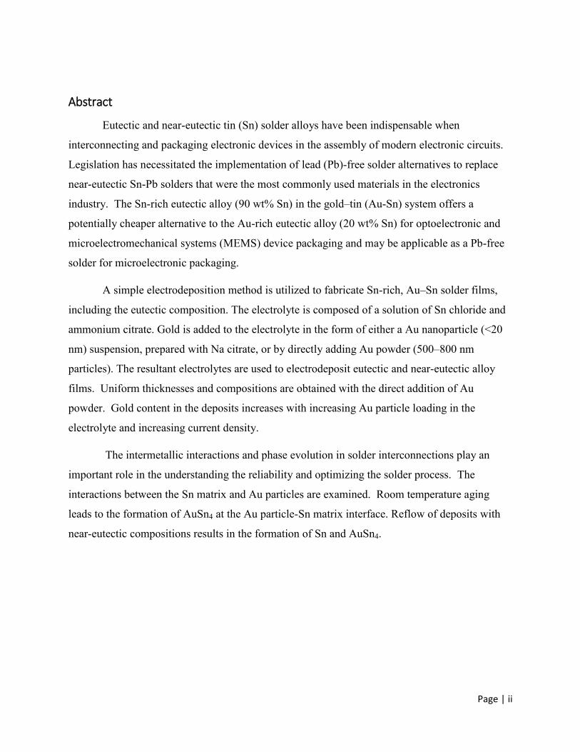
Abstract
Eutectic and near-eutectic tin (Sn) solder alloys have been indispensable when
interconnecting and packaging electronic devices in the assembly of modern electronic circuits.
Legislation has necessitated the implementation of lead (Pb)-free solder alternatives to replace
near-eutectic Sn-Pb solders that were the most commonly used materials in the electronics
industry. The Sn-rich eutectic alloy (90 wt% Sn) in the gold–tin (Au-Sn) system offers a
potentially cheaper alternative to the Au-rich eutectic alloy (20 wt% Sn) for optoelectronic and
microelectromechanical systems (MEMS) device packaging and may be applicable as a Pb-free
solder for microelectronic packaging.
A simple electrodeposition method is utilized to fabricate Sn-rich, Au–Sn solder films,
including the eutectic composition. The electrolyte is composed of a solution of Sn chloride and
ammonium citrate. Gold is added to the electrolyte in the form of either a Au nanoparticle (<20
nm) suspension, prepared with Na citrate, or by directly adding Au powder (500–800 nm
particles). The resultant electrolytes are used to electrodeposit eutectic and near-eutectic alloy
films. Uniform thicknesses and compositions are obtained with the direct addition of Au
powder. Gold content in the deposits increases with increasing Au particle loading in the
electrolyte and increasing current density.
The intermetallic interactions and phase evolution in solder interconnections play an
important role in the understanding the reliability and optimizing the solder process. The
interactions between the Sn matrix and Au particles are examined. Room temperature aging
leads to the formation of AuSn4 at the Au particle-Sn matrix interface. Reflow of deposits with
near-eutectic compositions results in the formation of Sn and AuSn4.

Page | iii
Dedication
To my family,
thank you for both your love and support.
Charles

Page | iv
Acknowledgements
I would like to acknowledge the contributions of my supervisor Dr. Ivey for his time, support
and guidance through the completion of my degree.
In addition, I acknowledge the help and guidance of Dr. Qi Liu, Dr. Anqiang He and Tina Baker
for all of their assistance.
I would also like to acknowledge funding from Natural Sciences and Engineering Research
Council (NSERC) of Canada and Micralyne, Inc.

Page | v
Table of Contents Chapter 1: Introduction ................................................................................................................................ 1
Chapter 2: Literature ..................................................................................................................................... 3
Life Cycle Analysis ..................................................................................................................................... 3
Processing Methods .................................................................................................................................. 4
The Metal-Electrolyte Interface ............................................................................................................ 6
Alloying Systems ....................................................................................................................................... 8
Sn-Pb Systems ....................................................................................................................................... 8
Pb-free Systems .................................................................................................................................. 10
Au-Sn System ...................................................................................................................................... 12
An-Sn Solders ...................................................................................................................................... 13
Sn-Rich, Sn-Au Solders ........................................................................................................................ 14
Gold Electrodeposition ....................................................................................................................... 14
Tin Electrodeposition .......................................................................................................................... 17
Research by Ivey et al ......................................................................................................................... 21
Research by Lee et al .......................................................................................................................... 24
Research by Barkey ............................................................................................................................. 27
Applications............................................................................................................................................. 29
Chapter 3: Experimental Procedures and Analytical Techniques ............................................................... 32
Electrolyte Preparation ........................................................................................................................... 32
Tin Electrolyte ......................................................................................................................................... 32
Gold Nano-particle Suspension ............................................................................................................... 33
Gold Nano-particle Electrolyte ............................................................................................................... 33
Gold Submicron Size Particle Electrolyte ................................................................................................ 34
Electrodeposition Process ....................................................................................................................... 34
Analytical Techniques ............................................................................................................................. 36
Sample Preparation for Scanning Electron Microscopy (SEM) ........................................................... 36
Scanning Electron Microscopy (SEM) ................................................................................................. 36
Secondary Electron (SE) and Backscattered Electron (BSE) Imaging .................................................. 36
Energy Dispersive X-Ray Spectroscopy (EDS) ...................................................................................... 37
Secondary Analytical Techniques............................................................................................................ 37
Zeta Potential ...................................................................................................................................... 37
Page | vi
X-ray Photoelectron Spectroscopy (XPS) ............................................................................................ 38
Transmission Electron Microscopy (TEM) ........................................................................................... 38
Chapter 4: Codeposition with Au Nano-Particles ....................................................................................... 39
Au nano-particle suspension................................................................................................................... 39
Nano-Au particle size determination ...................................................................................................... 39
Electrodeposition using Au nano-particles ............................................................................................. 41
Summary. ................................................................................................................................................ 50
Chapter 5: Codeposition using Sub-Micron Au Particles ............................................................................ 52
Submicron Au particles ........................................................................................................................... 52
Electrodeposition using submicron Au particles .................................................................................... 54
Summary ................................................................................................................................................. 60
Chapter 6: Phase Formation in Sn-rich, Sn-Au Deposits ............................................................................. 61
Phase distribution and composition ....................................................................................................... 64
Summary ................................................................................................................................................. 67
Chapter 7: Conclusions and Future Work ................................................................................................... 69
Final Conclusions ..................................................................................................................................... 69
Future Work ............................................................................................................................................ 70
References .................................................................................................................................................. 72
Page | vii
List of Tables
Table 1 Composition and Application Data for Selected Solders (Evans, 2007) ...................................... 11
Table 2 Typical Fluoborate Electrolyte Chemistries (Zhang, 2010) ......................................................... 18
Table 3 Typical Sulfate/Sulfuric Acid Electrolyte Chemistries (Zhang, 2010) .......................................... 19
Table 4 Typical Phenolsulfonic Acid Electrokyte Chemistries (Zhang, 2010) .......................................... 19
Table 5 Typical Halogen Electrolyte Chemistry (Zhang, 2010) ................................................................ 20
Table 6 Quantity of Additives Added to the Electrolyte ............................................................................. 48
Table 7 Summary of Particle Loading Effects on Deposit Composition.................................................... 58
Page | viii
List of Figures
Figure 1: Schematic of the electrical double layer (Zoski, 2007). ................................................................ 8
Figure 2: Pb-Sn binary phase diagram (American Society for Metals, 2012). ............................................. 9
Figure 3: Au-Sn binary phase diagram (American Society for Metals, 2012). .......................................... 13
Figure 4: SEM SE image showing the multi-layered deposit produced by Djufors and Ivey. Each layer
was deposited in sequence at 2.4 mA/cm2 for 5 min and 0.8 mA/cm
2 for 21 min (Djurfors & Ivey, 2002).
.................................................................................................................................................................... 22
Figure 5: SEM backscattered electron (BSE) plan view image (a) and cross sectional image (b) of the Au-
rich, eutectic Au-Sn alloy after reflow at 320°C for 5 min (Tang, 2008). .................................................. 23
Figure 6: SEM BSE cross-sectional image (a) and EDX spectrum (b) from the proeutectic phase of a Sn-
rich, hypoeutectic Au-Sn alloy (point 1) after reflowing at 250°C (Tang et al., 2008). ............................. 24
Figure 7: Plan view SE images of the sequentially deposited layers. a) Low magnification image of the as-
deposited Sn layer; b) high magnification image of the as-deposited Sn layer; c) low magnification image
of the deposit after Au deposition; d) high magnification image of the deposit after Au deposition (Kim
and Lee 2006). ............................................................................................................................................ 26
Figure 8: Cross-sectional BSE image of a sequentially deposited Sn-Au solder film (Kim and Lee, 2006).
.................................................................................................................................................................... 26
Figure 9: Sn-rich, Sn-Au reflowed soldered joint. a) Optical microscope image and b) SEM BSE image
(Kim and Lee 2006). ................................................................................................................................... 27
Figure 10: Proposed deposition sequence (Barkey, 2006). ......................................................................... 28
Figure 11: Sn-Ag deposited solder bumps. a) Particle additions less than 4g/L and b) particle additions
greater than 4 g/L (Barkey, 2006). .............................................................................................................. 28
Figure 12: Development of solder joints in relation to packaging architectures (Evans, 2007). ................ 30
Figure 13: Example of a ball-grid array. a) Low magnification image and b) high magnification image
(Evans, 2007). ............................................................................................................................................. 31
Figure 14: Various types of flip-chip joints (Evans, 2007). ........................................................................ 31
Figure 15: Schematic representation of the citrate layer surrounding the Au nano-particles (McFarland et
al., 2004). .................................................................................................................................................... 34
Figure 16: Schematic of the Electrochemical Cell ...................................................................................... 35
Figure 17: Distribution of Au nano-particle diameters using ZetaPlus sizing software. (The x-axis is
displayed on a log scale.) ............................................................................................................................ 40
Figure 18: Indexed electron diffraction pattern (left) and TEM bright field image of Au nano-particles
(right). ......................................................................................................................................................... 40
Figure 19: SEM SE images of a deposit on a Pt metallized substrate produced from a fresh electrolyte
mixed with the Au nano-particle suspension. Image (a) is a low-magnification plan-view image, whereas
image (b) is a higher magnification cross-sectional view. .......................................................................... 41
Figure 20: EDS spectrum from the deposit shown in Figure 18. ................................................................ 42
Figure 21: SEM SE images of a deposit produced using an aged electrolyte mixed with the Au nano-
particle suspension. Images (a) and (b) are plan-view and cross-sectional view images, respectively. .... 42
Figure 22: EDS spectrum from the deposit shown in Figure 20. ................................................................ 42
Figure 23: SEM SE images of deposit fabricated using an aged Sn electrolyte mixed with the Au nano-
particle suspension, without magnetic stirring. Images (a) and (b) are plan-view and cross-sectional view
images, respectively. ................................................................................................................................... 43
Figure 24: EDS spectrum from a Au nano-particle cluster in Figure 22a (circled region). ........................ 44
Page | ix
Figure 25: SEM BSE images of deposits fabricated from an electrolyte with an increased amount of Au
nano-particles. Images (a) and (b) are a plan-view and cross-sectional view, respectively, of a deposit
from an electrolyte with an Au to Sn ratio of 1:125. Images (c) and (d) are a plan-view and cross-
sectional view, respectively, of a deposit from an electrolyte with an Au to Sn ratio of 1:166. ................. 45
Figure 26: SEM BSE images of deposits fabricated using a reduction of Sn in the electrolyte. Images (a)
and (b) are a plan-view and cross-sectional view, respectively of a deposit from an electrolyte with an Au
to Sn ratio of 1:125. Images (c) and (d) are a plan-view and cross-sectional view, respectively, of a
deposit from an electrolyte with an Au to Sn ratio of 1:50. ........................................................................ 46
Figure 27: SEM SE plan-view image of a deposit from an electrolyte without the addition of tri-
ammonium citrate. ...................................................................................................................................... 47
Figure 28: SEM SE images of a deposit using an electrolyte containing sodium citrate in place of
ammonium citrate. Images (a) and (b) are a plan-view and cross-sectional view, respectively. ............... 48
Figure 29: SEM BSE images of deposit morphology improvements with additives to the nano-Au particle
containing electrolyte. ................................................................................................................................. 49
Figure 30: SEM BSE image of a deposited fabricated from an electrolyte containing a leveler.
Agglomerated Au nano-particles are present on the surface. ..................................................................... 50
Figure 31: a) SEM SE image of submicron Au particles. b) Corresponding EDS spectrum from the same
Au particles. ................................................................................................................................................ 53
Figure 32: XPS spectrum from the submicron Au particles. ...................................................................... 53
Figure 33: SEM SE images comparing deposits from Sn electrolytes with and without Au particles.
Images (a) and (b) are a plan-view and a cross-sectional view, respectively, of a deposit from an Sn
electrolyte. Images (c) and (d) are a plan-view and a cross-sectional view, respectively, of a deposit from
a Sn electrolyte with direct addition of submicron Au particles (1 g/L). .................................................... 54
Figure 34: SEM SE images showing the effects of current density on Au incorporation using a Sn
electrolyte with 1 g/L submicron Au particle loading. Images (a) and (b) are a plan-view and cross-
sectional view, respectively, of a sample fabricated using a current density of 5 mA/cm2. Images (c) and
(d) are a plan-view and cross-sectional view, respectively of a sample fabricated using a current density of
7.5 mA/cm2. Images (e) and (f) are a plan-view and cross-sectional view, respectively, of a sample
fabricated using a current density of 10 mA/cm2. Images (g) and (h) are a plan-view and cross-sectional
view, respectively, of a sample fabricated using a current density of 15 mA/cm2. .................................... 56
Figure 35: SEM SE images for direct current deposition using a Sn electrolyte with 1 g/L submicron Au
particle loading. Image (a) is a plan-view of a sample created using a current density of 7.5 mA/cm2.
Image (b) is a plan-view of a sample created using a current density of 15 mA/cm2. ................................ 57
Figure 36: The effect of multiple depositions from the same electrolyte, without additional submicron Au
particles, on deposit composition. The initial electrolyte was composed of 75 g/L (NH4)3HC6H5O7, 50
g/L SnCl2•2H20 and 0.75 g/L of submicron Au particles. The current density was 7.5 mA/cm2. ............. 59
Figure 37: The effect of multiple depositions from the same electrolyte deposits, with additional
submicron Au particles introduced after each deposit, on deposit composition. The initial electrolyte was
composed of 75 g/L (NH4)3HC6H5O7, 50 g/L SnCl2•2H20 and 0.75 g/L submicron Au particles. The
current density was 7.5 mA/cm2 ................................................................................................................. 59
Figure 38: SEM BSE cross section image of Sn-Au deposit after aging for 2 weeks at room temperature.
Interdiffusion between Sn and the Au nanoparticles is evident. The electrolyte contained 75 g/L
(NH4)3HC6H5O7 and 50 g/L SnCl2•2H20, with 0.75 g/L of Au particles, and deposition was done for 90
min at 7.5 mA/cm2. ..................................................................................................................................... 61
Figure 39: EDS analysis of the different phases present in the sample from Figure 38. ........................... 62
Page | x
Figure 40: SEM BSE images (cross-section and plan-view) of Sn-Au deposits after aging at elevated
temperatures below the eutectic temperature. The deposit in images (a) and (b) was exposed to 100°C for
1 min. The deposit in images (c) and (d) was exposed to 150°C for 1 min. The deposit in images (e) and
(f) was exposed to 200°C for 1 min. ........................................................................................................... 63
Figure 41: SEM BSE images of samples annealed above the eutectic temperature. The deposit in images
(a) and (b) was heated to 250°C for 1 min. The deposit in images (c) and (d) was heated to 260°C for 1
min. The deposit in images (e) and (f) was heated to 270°C for 1 min. .................................................... 64
Figure 42: SEM BSE images of a sample deposited using a particle loading of 0.75 g/L Au at a current
density of 7.5 mA/cm2. The sample initially had an as deposited composition of 10 wt% Au and after
reflow at 250°C for 1 min the final composition was 24 wt% Au. Images denoted as (a) and (b) are higher
magnification images of the two different types of structures visible in the deposit. ................................. 66
Figure 43: SEM BSE images of a sample the was deposited using a Au particle loading of 0.75 g/L and a
current density of 7.5 mA/cm2. The sample had an as deposited composition of 4.56 wt% Au and after
reflow at 250°C for 1 min the final composition was 9.88 wt% Au. The sample was subjected to a sonic
wash prior to reflow. Image (a) is a low-magnification image and image (b) is a higher magnification
image of the circled region in image (a). .................................................................................................... 67
Figure 44: SEM BSE cross-sectional images of a solder film that has undergone a sonic wash process
before reflow. Images (a) and (b) are located at the edge and center of the deposit, respectively. ........... 67
Page | 1
Chapter 1: Introduction
Gold-tin eutectic alloy solders are commonly used for optoelectronic device and
microelectromechanical system (MEMS) packaging (Kim and Lee, 2005). The Au–Sn phase
diagram has two eutectics, one which is Au-rich at 20 wt% Sn with a eutectic temperature of
280°C and another which is Sn-rich at 90 wt% Sn with a eutectic temperature of 217°C. The
industry standard is the former eutectic, which is considered a hard solder, and has an excellent
combination of mechanical and thermal properties (Kim and Lee, 2005). The Sn-rich eutectic
composition is a potential lower cost alternative and may also be a candidate Pb-free solder for
microelectronic applications, because of its relatively low melting temperature (217°C) (Kim and
Lee, 2005 & Lee and Chuang, 2003). The Sn-rich eutectic does have some limitations, however.
In particular, Sn-rich, Au–Sn alloys oxidize easily and the AuSn4 intermetallic, which forms
upon solidification after reflow, is brittle (Kim and Lee, 2005). However, according to Lee and
Chuang (2003) the Sn-rich eutectic has suitable properties to be used for packaging applications,
and its use would significantly reduce material costs. Several methods can be utilized to fabricate
solder films.
Chapter 2 is the literature review presenting a life cycle analysis that outlines the
legislations leading to Pb-free solder alternatives that will replace near-eutectic Sn-Pb solders
most commonly used in the electronics industry. Of these methods, electrodeposition offers the
best combination of cost effectiveness and process control particularly for solder deposited onto
patterned wafers (Sun and Ivey, 1999). For the Sn-rich composition, a limited amount of work
has been done, either through vacuum deposition or sequential electrodeposition of Au and Sn
from two separate electrolytes (Jeong et al, 2006 & Kim et al, 2006 & Tang et al 2008 & He et
al, 2012). The main concern with sequential electrodeposition is that deposits are exposed to air
during transfer from one electrolyte to the other. This exposure is of particular concern for Sn, as
it oxidizes readily in air. A recent publication has demonstrated that Sn-rich, Au–Sn alloys can
be deposited from a single electrolyte consisting of Au and Sn chloride salts, as well as Na
sulfite, ammonium citrate and other additives (He et al, 2012).
Chapter 3 outlines the experimental design used to create the electrolytes and the
analytical techniques used to analyze the deposits. Small batches of the simple, “green”
Page | 2
electrolyte Sn electrolyte were prepared using Sn chloride and ammonium citrate (He and Ivey,
2008). Following the Sn electrolyte preparation, the electrolytes used in Chapters 4 and 5 are
discussed. Lastly, each analytical technique used to complete the analysis of the deposits are
described in detail.
Chapter 4 discusses the electrodeposition process using a simple, “green” electrolyte
composed of a solution of Sn chloride and ammonium citrate developed previously (He and Ivey
2008). The addition of Au to the electrolyte occurs in the form of an Au nanoparticle (<20 nm)
suspension prepared with sodium citrate.
In Chapter 5, a simpler approach is taken to electrodeposit Sn-rich, Au–Sn solders,
including the Sn-rich eutectic. The same Sn electrolyte as that in Chapter 3 is used; however, Au
is incorporated through the direct addition of Au powder (500–800 nm particles). Using Au
particles keeps the solution simple, as there is only one species to be reduced.
Interactions between the Sn matrix and Au particles are examined in Chapter 6.
Intermetallic interactions and phase evolution of the Sn-rich, Sn-Au solder films are discussed,
specifically the as-deposited composition is compared with the composition after reflow. The
importance of understanding the reliability and optimization of the solder process is discussed as
well.
Chapter 7 summarizes the results for the work completed to develop a simple process for
the electrodeposition of Sn-rich, Au-Sn solder films, highlighting the importance characteristics
of the proposed Sn-rich Au-Sn solder composition while reinforcing the key results from the
work. Lastly, potential future work is proposed.
Page | 3
Chapter 2: Literature
Life Cycle Analysis
Near-eutectic Sn-Pb solders were historically the most common soldering materials used
in the electronics industry. Sn-Pb solders are desirable due to their low melting temperature,
good workability, ductility, and excellent wetting (Evans, 2007). Eutectic and near eutectic tin
lead alloys had become indispensable when interconnecting and packaging electronic devices in
the assembly of modern electronic circuits. However, Pb processing and reclamation can have
negative effects on the surrounding environment. Moreover, Pb is toxic if ingested into the
human body. Major steps have been taken to reduce or eliminate Pb from specific fields in the
industry. The European Union directives on Waste Electrical and Electronic Equipment
(WEEE) state that components sold in the European Union must be Pb-free as of July 1, 2006
(Nimmo, 2002 & Gamalski, 2002). Major firms in Japan have been following the Japanese
Ministry of Trade (MITI) legislation, which proposed take-back legislation in 1998 requiring
manufactures to recover harmful materials in consumer grade production. Further reduction of
harmful materials was mandated by MITI, which determined that the amount of lead used in
commercial grade electronics must be reduced by half from 1996 to 2000 and to one-third by
2005 (Le Fevre, 2002). Korea has also started to develop products including handhelds and
white goods with alternative alloy solders attempting to reduce Pb consumption (Evans, 2007).
Within the United States, the Environmental Protection Agency has no official legislation on this
matter but rather has strongly encouraged manufactures to reduce their hazardous wastes (Ku,
2003). To achieve these goals, potential replacements for Sn-Pb solder alloys include binary,
ternary, and some quaternary alloys of Sn using Ag, Zn, In, Sb, and Cu (Evans, 2007).
Legislation has led to Pb-free solder alternatives and further studies have been completed on
these systems looking at the potential environmental and human impacts. These studies have
involved a total Life Cycle Analysis (LCA) of Pb-free solders (Ku, 2003 & Turbini, 2001 &
Zhou, 2008). This design approach uses the philosophy of industrial ecology by means of
studying economics, green engineering, and sustainable development.
The concept of industrial ecology is one in which economic systems are viewed not in
isolation from their surrounding systems but in concert with them... As applied to
industrial operations, it requires a systems view in which one seeks to optimize the total
Page | 4
industrial materials cycle from virgin material, to finished material, to component, to
product, to waste product, and to ultimate disposal. Factors to be optimized include
resources, energy, and capital. (Wenzel, 1997)
A conventional LCA process can generate results subject to multiple interpretations.
Despite this drawback, the advantages of this process enjoy wide recognition (Zhou, 2008). In
practice, LCA analysis tends to stop at the level of inventory analysis or characterization (Zhou,
2008). Many other factors (economic, ideological, political, and social) are involved; the
remaining steps of normalization, grouping, and weighting are not well defined in the global
context (Zhou, 2008). Since conventional LCA processes are outside the scope of this thesis,
only a brief description covering a LCA methodology for Pb-free solders is given as an
introduction to the development of alternative solder materials. Ku (2003) used a qualitative,
matrix based method developed by Allenby (1992) as the basis to compare information between
Pb and six alternative metals (Ku, 2003). Designed and weighted metrics were created for
toxicity and public health impact, availability and raw material supply, and environmental impact
were compared to give supporting documentation to support decisions made in selecting
alternative materials. However, depending on the required mechanic properties, each individual
manufacturer can use other possible Pb-free solders as well.
Continuing with the LCA analysis, the next remaining stages can be investigated. A
closer look at possible decision criteria such as processing methods, alloying systems, and
current research in the field will be summarized.
Processing Methods
Processing methods used for mass manufacturing are important considerations when
looking at possible new chemistries. Though there are a wide variety of application methods, the
main processing method of focus is electrodeposition. Electrodeposition, or electroplating, is an
economical and valid technology for producing solder deposits. Electrodeposition is the process
of depositing a coating with specific characteristics by means of electrolysis (Lowenhein, 1974).
The laws of electrolysis, formulated by Faraday, remain the foundation for this process. Simply
Page | 5
stated, electrodeposition is the reduction of a metal ion Mz+
from an aqueous electrolyte
represented by the following chemical reaction:
𝑀𝑧+ + 𝑧𝑒− → 𝑀 (1)
Electrochemical cells are one of the basic tools that can be used to study processes and
factors that affect the transport of charge across the interface between chemical phases (Bard and
Faulkner, 2001). An electrochemical cell contains a reference electrode, a working electrode,
and an ionic conductor (an electrolyte). The two electrodes are connected by a conducting wire
through a power source. A potential difference is created by an external source, supplying
additional electrons to the cathode or an electroless (autocatalytic) process in which the reducing
agent in electrolyte acts as the electron source creating a reduction reaction (Paunovic and
Schlesinger, 1998). Ions in the electrolyte are then attracted to the cathode where they are
incorporated into the metal lattice (Lowenheim, 1974). Charge transport is achieved by the
movement of electrons (or holes) and ions supplied by the electrolyte. The overall chemical
reaction takes place in two independent half cell reactions at each electrode. However, the rate
limiting step during practice is harder to determine since the electrolyte is being altered during
deposition. The rates are driven by the potential differences existing at the metal-electrolyte
interface (Lowenheim, 1974). For each system there is a specific potential and temperature for
which the two competing rates are equal (Lowenheim, 1974). This equilibrium potential is
dependent on temperature and concentration or activity of the ions in the electrolyte
(Lowenheim, 1974). The equilibrium potential at the electrode where the reduction reaction
from Equation 1 takes place is given by the Nernst Equation:
𝐸 = 𝐸𝑀𝑛+0 +
𝑅𝑇
𝑛𝐹𝑙𝑛𝑎𝑀𝑛+ (2)
in which E is the electrode potential, Eo is the standard potential of the reduction reaction, R is
the gas constant, T is the absolute temperature, F is the Faraday’s constant, η is the charge of the
ion, and α is the activity of the metal ion in electrolyte. Variables, such as temperature (T),
pressure (P), and ion concentration in the electrolyte are important for the consistent performance
of any deposition bath. Small deviations can be sufficient to adversely affect plate quality,
deposition rates, and other properties. In addition, the length of deposition time (t) controls the
degree to which the reaction takes place.
Page | 6
Current efficiencies are important in practical applications, such as electrorefining and
electroplating applications, where the mass of the metal deposited or dissolved is important
(Paunovic and Schlesinger, 1998). In electroplating, current efficiency can depend on a number
of parameters including: plating bath chemistry, pH, agitation, and current density (Paunovic and
Schlesinger, 1998). Current efficiency (CE) mathematically, shown in Equation 3, is the ratio of
the actual amount of metal deposited or dissolved, Ma, to the theoretically amount determined
from Faraday’s law, Mt.
𝐶𝐸 = 𝑀𝑎
𝑀𝑡 (3)
The applied potential (E) or current (i) are important considerations for electrodeposition
methods and some of the main factors controlling the process. The amount of potential applied to
the system can affect the quantity of electricity (Q), controlling which species in the electrolyte
will react or be electrolyzed. Ideally the cathode and anode current efficiency should be equal
leaving the electrolyte at a constant equilibrium. A deposit created in this ideal manner should
have a specified brightness, hardness, ductility, and internal stress (Lowenheim, 1974).
The Metal-Electrolyte Interface
The metal-electrolyte interface involves two components: an electrode and an electrolyte
in the case of an electrodeposition cell. Where the desired reduction reaction takes place is
considered the “working electrode”, while a “counter electrode” completes the circuit providing
a standard reference that can be used to monitor potential changes in the system (Doesburg,
2000). At the “counter electrode”, the following reactions can occur: metal dissolution, oxygen
evolution, oxidation, or passivation (Doesburg, 2000). These interactions fall under two
categories: Faradaic and non-Faradaic processes. Faradaic processes are governed by Faraday’s
law and involve reactions in which charges are transferred across a metal-electrolyte interface.
𝑄 = 𝑛𝐹𝑁 (4)
where Q is the quantity of electricity applied, n is the stoichiometric number of electrons
involved in the chemical reaction occurring at the electrode, F is Faraday’s constant (96485.3
coulombs/mole of electrons), and N is the number of moles electrolyzed.
Page | 7
Non-faradaic processes such as adsorption and desorption can occur at the electrolyte-
electrode interface causing the electrode interface to change with changing potential or
electrolyte composition (Bard and Faulkner, 2001). These processes occur when a charge does
not cross the interface (Bard and Faulkner, 2001). However, external currents can flow when the
potential, electrode area, or electrolyte composition changes (Bard and Faulkner, 2001). When
no charge transfer occurs across the metal electrolyte interface, no matter the imposed potential
caused by the external power source, the electrode is called an ideal polarized electrode (IPE)
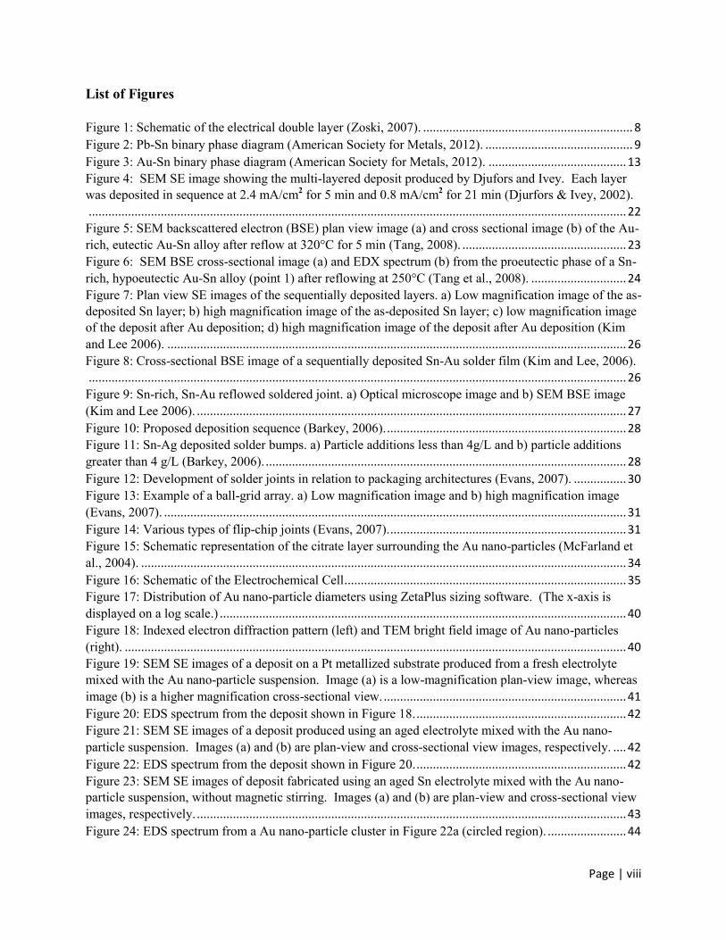
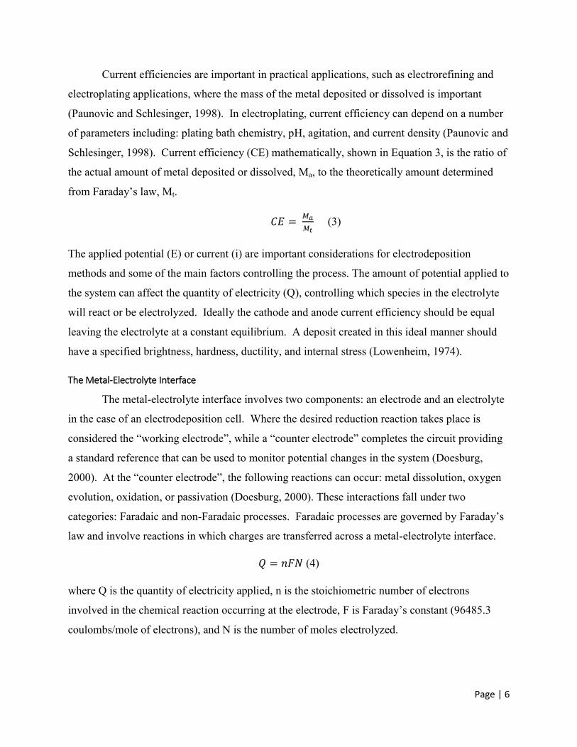
(Bard and Faulkner, 2001). The closest layer to the electrode contains solvent molecules and
sometimes other species that are specifically adsorbed on the surface of the electrode (Figure 1).
This “inner layer” is also known as the compact, Helmholtz, or Stern layer (Bard and Faulkner
2001). The electrical center of the specifically adsorbed ions is called the inner Helmholtz plane
(IHP) at a distance x1 (Bard and Faulkner, 2001). The solvate ions can approach only to a
distance x2, which in called the outer Helmholtz plane (OHP) (Bard and Faulkner, 2001).
Nonspecifically adsorbed ions are distributed in the electrolyte extending from the OHP into the
bulk of the electrolyte called the diffuse layer (Bard and Faulkner, 2001). Electrode processes
will be affected by the structure of the double layer (Bard and Faulkner, 2001). Absorbed ions,
solvated charges species, and oriented dipoles form at the interface of the electrode. This
formation of charges species is referred to as the electrical double layer capacitance (Bard and
Faulkner, 2001). An electrical double layer at the interface of the electrode and electrolyte can
be approximated as a capacitor (Bard and Faulkner, 2001). In order for deposition to occur a
charge must be applied to the electrical double layer to raise its potential to the required value for
metal deposition (Bard and Faulkner, 2001).
Page | 8
Figure 1: Schematic of the electrical double layer (Zoski, 2007).
Alloying Systems
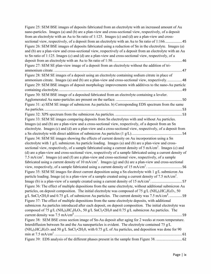
Sn-Pb Systems
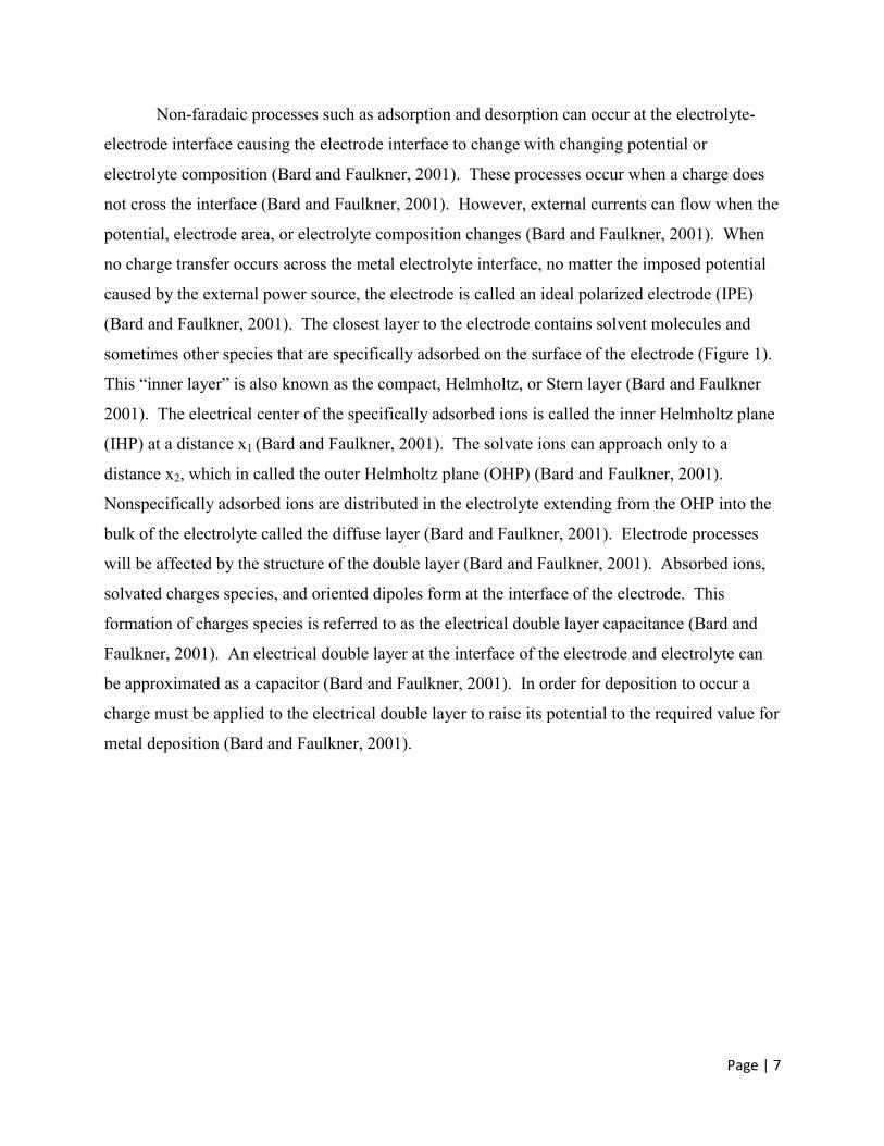
The majority of understanding with regard to electronic reliability comes from devices
fabricated using Sn-Pb solders. Sn-Pb solders, specifically the 63 wt% Sn – 37 wt% Pb and 60
wt% Sn – 40 wt% Pb near eutectic solders (Figure 2), were the solder of choice at the beginning
of electronics manufacturing. The metallurgy of the Sn-Pb alloy system is generally
representative of all the soldering alloys in that it is a eutectic system. In a typical eutectic
system, the solubility of one solid solution transitions to a much more limited solubility of the
other alloying element. The highest temperature at which a metal or alloy is completely solid is
called the solidus curve. While the lowest temperature at which the system is completely liquid
is called the liquidus curve. At the extreme of the phase diagram are the pure metals. The
temperature differential between the solidus and liquidus curves is called the melting or freezing
range and within this range the alloy is partially melted or solidified. The two phases are usually
distinguishable from one another and typically consist of layers or laminations to produce a
“lamellar structure” consistent with a eutectic alloy.
Page | 9
Figure 2: Pb-Sn binary phase diagram (American Society for Metals, 2012).
Sn-rich, Sn-Pb solder was chosen due to its superior properties among low melting point
solders, superior manufacturing, and process compatibility (Evans, 2007). Near eutectic alloys
of the Sn-Pb system are well suited for machine-soldering and mass-soldering methods and are
still considered the best alternative for certain applications (Evans, 2007). There are many other
important solder compositions in the Sn-Pb systems that should be highlighted:
5 wt% Sn – 95 wt % Pb solder composition has a relatively high melting temperature,
has a narrow melting and freezing range, and is poor in terms of wetting and flow
compared with higher Sn alloys. However, the mechanical properties of this high-Pb
alloy are better at 149°C (300°F) than most other alloys with more Sn.
The 10 wt% Sn – 90 wt% Pb, 15 wt% Sn – 85 wt% Pb, and 20 wt% Sn -80 wt% Pb
solders have progressively lower liquidus and solidus temperatures, a wider melting
range, and better flow than 5 Sn – 95 Pb. All are prone to solidification cracking or "hot
tearing".
Page | 10
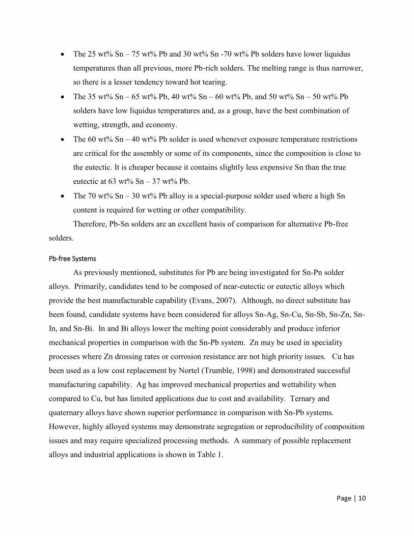
The 25 wt% Sn – 75 wt% Pb and 30 wt% Sn -70 wt% Pb solders have lower liquidus
temperatures than all previous, more Pb-rich solders. The melting range is thus narrower,
so there is a lesser tendency toward hot tearing.
The 35 wt% Sn – 65 wt% Pb, 40 wt% Sn – 60 wt% Pb, and 50 wt% Sn – 50 wt% Pb
solders have low liquidus temperatures and, as a group, have the best combination of
wetting, strength, and economy.
The 60 wt% Sn – 40 wt% Pb solder is used whenever exposure temperature restrictions
are critical for the assembly or some of its components, since the composition is close to
the eutectic. It is cheaper because it contains slightly less expensive Sn than the true
eutectic at 63 wt% Sn – 37 wt% Pb.
The 70 wt% Sn – 30 wt% Pb alloy is a special-purpose solder used where a high Sn
content is required for wetting or other compatibility.
Therefore, Pb-Sn solders are an excellent basis of comparison for alternative Pb-free
solders.
Pb-free Systems
As previously mentioned, substitutes for Pb are being investigated for Sn-Pn solder
alloys. Primarily, candidates tend to be composed of near-eutectic or eutectic alloys which
provide the best manufacturable capability (Evans, 2007). Although, no direct substitute has
been found, candidate systems have been considered for alloys Sn-Ag, Sn-Cu, Sn-Sb, Sn-Zn, Sn-
In, and Sn-Bi. In and Bi alloys lower the melting point considerably and produce inferior
mechanical properties in comparison with the Sn-Pb system. Zn may be used in speciality
processes where Zn drossing rates or corrosion resistance are not high priority issues. Cu has
been used as a low cost replacement by Nortel (Trumble, 1998) and demonstrated successful
manufacturing capability. Ag has improved mechanical properties and wettability when
compared to Cu, but has limited applications due to cost and availability. Ternary and
quaternary alloys have shown superior performance in comparison with Sn-Pb systems.
However, highly alloyed systems may demonstrate segregation or reproducibility of composition
issues and may require specialized processing methods. A summary of possible replacement
alloys and industrial applications is shown in Table 1.
Page | 11
Table 1 Composition and Application Data for Selected Solders (Evans, 2007)
Alloy
System
Nominal Composition of
Selected Alloys (wt%)
Melting Range (°C) Application Remarks
Solidus Liquidus
Sn-Pb 63wt%Sn37 wt%Pb (e) 183 183 Primary joining alloy for
electronic assembly. 60 wt%Sn40 wt%Pb 183 191
62 wt%Sn36 wt%Pb2
wt%Ag (e)
179 179
Pb-Sn 95 wt%Pb5 wt%Sn 308 312 High-temperature solders for
die attachment. 90 wt%Pb10 wt%Sn 268 301
Pb-Sn-
Ag
97.5 wt%Pb1 wt%Sn1.5
wt%Ag (e)
305 305
82.5 wt%Pb15
wt%Sn2.5 wt%Ag
275 280
Pb-In 75 wt%Pb25 wt%In 226 264 High-temperature solders.
50 wt%Pb50 wt%In 180 210
Sn-Ag 96.5 wt%Sn3.5 wt%Ag
(e)
221 221 Primary replacement
candidates for near-eutectic
SnPb alloys; high melting
point.
Sn-Ag-
Cu
95.5 wt%Sn3.8
wt%Ag0.7 wt%Cu (e)
217 217
95.5 wt%Sn3.9
wt%Ag0.6 wt%Cu
~217 ~217
Sn-Bi 42 wt%Sn58 wt%Bi (e) 138 138 Low melting point eutectic;
potential segregation problems;
low melting temperature phase
with trace of Pb.
Sn-Bi-
Ag
93.5 wt%Sn3 wt%Bi3.5
wt%Ag
206 213 Replacement candidates for
near-eutectic SnPb alloys;
potential segregation and
cracking problems with
increasing Bi content; low
melting point phase with trace
Pb.
91.5 wt%Sn5 wt%Bi3.5
wt%Ag
- -
90.5 wt%Sn7.5 wt%Bi2
wt%Ag
207 212
76 wt%Sn22 wt%Bi2
wt%Ag
- -
Sn-Bi-In 70 wt%Sn20 wt%Bi10
wt%In
189 199
Page | 12
Sn-Cu 99.3S wt%n0.7 wt%Cu
(e)
227 227 Low cost; plumbing alloy; poor
mechanical properties.
Sn-Zn 91 wt%Sn9 wt%Zn (e) 198.5 198.5 Zn imparts poor corrosion
resistance and reduced
wettability; Zn has low vapor
pressure leading to segregation
in wave pots; Ag alloying may
improve SnZnIn ternary
properties; Cu alloying may
improve SnAgZn.
Sn-Zn-Bi 89 wt%Sn8 wt%Zn3
wt%Bi
189 199
Sn-Zn-In 87 wt%Sn8 wt%Zn5
wt%In
~188 ~188
Sn-Zn-
Ag
95.5 wt%Sn1 wt%Zn3.5
wt%Ag (e)
217 217
Sn-In 48 wt%Sn52 wt%In 117 117 In adds cost; specialized
applications for wetting
ceramics and glasses.
50 wt%Sn5 wt%0In 117 125
Sn-In-Ag 77.2 wt%Sn20 wt%In2.8
wt%Ag
In-Ag 90wt%In10 wt%Ag 141 237 High cost
Sn-Sb 95 wt%Sn5 wt%Sb 235 240
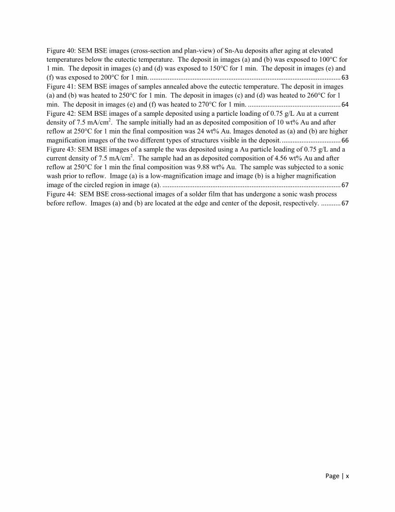
Au-Sn System
Gold’s high electronic conductivity, low contact resistance, and good solderability make
it an ideal choice for electrical and electronic hardware (Reid, 1974). An Au-rich, Au-Sn
eutectic solder is often used for specialty applications. The 80 wt% Au 20 wt% Sn eutectic
solder is composed of ζ (Au5Sn) and δ (AuSn) with a eutectic temperature of 278°C (Figure 3)
(American Society of Metals, 2012). This Au-rich eutectic composition is classified as a hard
solder due to the high melting temperature of Au. Analysis has shown that the Au-rich eutectic
composition has good creep behaviour and creep resistance (Reid, 1974 & Sun and Ivey, 2001).
Furthermore, due to its high electrical conductivity, low contact resistance, and good
solderability, 80Au20Sn has been used for specific applications in electronics (Reid and Goldie,
1974).
Page | 13
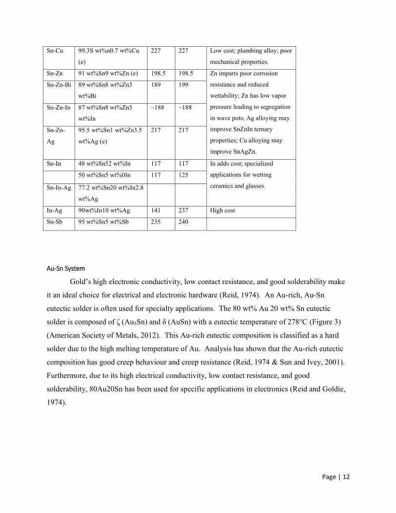
Figure 3: Au-Sn binary phase diagram (American Society for Metals, 2012).
An-Sn Solders
Au – Sn eutectic solders have been produced in sequential layers by depositing an Au
seed layer followed by a Sn layer (Kallmayer et al, 1995 & Zakel et al, 1995). Au and Sn
electrolytes are readily available commercially and are utilized to deposit these layers. Au and
Sn co-deposition from a single electrolyte offers an economical advantage over sequential
plating. Electroplating electrolyte chemistries can be altered to stabilize the co-deposition bath.
Both acidic and alkaline electrolytes have been developed, with the primary focus towards acidic
electrolytes for co-deposition of the Au-Sn system.
Co-deposition from a cyanide system using pyrophosphate as a buffering agent has been
studied with a basic formula consisting of K4P2O7, KAu(CN)2, and SnCl22H2O (Kubota, 1983).
The investigation was focused on the mass transfer reaction mechanisms between monovalent
Au or bivalent Sn and pyrophosphate ions by measuring conductivity, kinematic viscosity and
limiting current density of eletrodeposition (Sun & Ivey, 1999).
Various Au-Sn compositions have been electrodeposited from cyanide electrolytes
containing HAuCl4H20, K2SnO33H2O, KCN, and KOH. Investigation did not yield a linear
Page | 14
relationship between the Sn content in the electrolyte and the Sn content formed in the deposit.
Instead a relationship was found between the two alloys, which permitted formation of the
desired compositions (Tanabe et al, 1983). Development of non-cyanide based electrolytes has
been challenging, yet has yielded some success. A major challenge with the development of
non-cyanide electrolytes is the lack of a strong Au complexing agent. Other challenges in co-
deposition of the Au-Sn system can arise due to the oxidation of stannous ions to stannic ions in
the electroplating bath - such oxidation can be caused by either atmospheric oxygen or anode
oxidation (Schlesinger and Paunovic, 2000).
Sn-Rich, Sn-Au Solders
The Au-Sn system has a second eutectic composition, which is Sn-rich and shown in
Figure 3, that may be a candidate Pb-free solder to be used in microelectronic applications. The
Sn-rich, Sn-Au solder composition is not currently used in the industry. This allows for the
opportunity to explore an alternative composition for solder joints in optoelectronic and MEMS
applications and to develop cheaper alternatives to the Au-rich solder (Lee, 2003 & Lee, 2005).
According to Lee, 2003 the Sn-rich eutectic composition has suitable properties to be used for
packaging applications, and its use would significantly reduce material costs. Its most
interesting property is its ability to plastically deform under stress without failing under normal
usage. Tang, 2008 explored solidification and intermetallic formation of Sn-Au couples. This
particular composition range does have some drawbacks, however, as Sn-rich, Sn-Au alloys
oxidize easily and the AuSn4 intermetallic that forms upon solidification after reflow is often
brittle (Lee, 2005).
Gold Electrodeposition
The type of electrolyte can be further classified depending on the basis of application.
Whether Au is being deposited for its color or industrial use will affect the technological
requirements (Reid,1974). “Color golds” have a limited interest in the field and are typically
used in thin “flash like” deposits. “Industrial golds” are used for functional purposes where
processes are described as pure Au or bright alloy Au (Reid, 1974). Initially, industrial baths
containing 22.5 - 26 g/L of Au were recommended (Volk, 1957 & Raub, 1967). Pure Au
electrolytes have not changed much since the 1960s; additions of potassium hydroxide and the
Page | 15
use of ammonium gold cyanide with the application of ultrasonics have made improvements
(Reid, 1974). Bright alloy Au deposits involve the codeposition of Ag, Sn, and Sb (Reid, 1974).
Alkaline Cyanide Baths
Originally alkaline baths were used for commercial Au plating, i.e., since the 1840’s
(Foulke, 1969). Alkaline cyanide baths operate at a high pH with an excess of free cyanide.
Typically, potassium gold cyanide is used as a source of free cyanide in these baths. The
cyanide released during the deposition does not significantly alter the cyanide concentration in
the bath. Shifting the potential of Au (I) cyanide due to accumulation of free cyanide does not
occur. The excess cyanide permits the use of gold anodes for the replenishment of the metal
plated from the bath:
Cathode: [Au(CN)2]- + e- → Au + 2CN
-
Anode: Au + 2CN- → [Au(CN)2]
- + e
-
Full cell: No change to plating electrolyte
The main changes that occur in the bath are due to oxidation or reduction side reactions, drag-out
of plating salts, and drag-in of water or impurities. The free cyanide promotes the corrosion of
the gold anode forming [Au(CN)2]-, increases the throwing power, and improves the
conductivity.
Neutral Cyanide Electrolytes
Non-alkaline baths exhibit a wider range of physical and chemical properties than
possible at higher pH levels. Although the metals used to harden Au are not readily codeposited
from neutral pH baths, they can be formed using a careful selection of plating parameters without
the use of additives. In neutral baths the gold salt used is the same as for alkaline and acid baths,
KAu(CN)2. Neutral pH and the absence of free cyanide create favorable formulations for the use
of photoresist and other polymeric materials. Typically, a pure soft gold can be produced using
neutral baths at relatively low current densities. The phosphate salts serve as a supporting
electrolyte and pH control causing less concern regarding concentration control.
Additive free hard gold (AFHG) can be produced from neutral baths using phosphate as the
buffer. The advantages of AFHG baths over metal hardened baths are:

Page | 16
No need to control additive concentration;
High current efficiency;
Greater tolerance for heavy metal impurities due to the insolubility of many metal
phosphates;
High ductility and thermally stable contact resistance for electronic components.
Although there are advantages to AFHG baths, there are some susceptibilities to contamination,
mainly to small impurities such as Ni, Co, and Fe ions that can cause large changes to the
physical properties of the deposits.
Acid Cyanide Electrolytes
These electrolytes were originally developed for the jewelry trade but are now being used
throughout the electronics industry. An advantage of using acidic electrolytes is that photoresist
and other polymers can be used as templates (Foulke, 1969). Typically, platinized Ti, Au, or
Au-plated platinized Ti are used for the anodes in these baths. The use of gold plated electrodes
is found to not readily dissolve at low current densities due to a low free cyanide concentration
created at low current densities. If high current densities and a low electrolyte volume are
present, concentrations of free cyanide can build in the electrolyte and lead to oxidation and
dissolution of a pure gold or gold plated anode. In these situations insoluble anodes can be used
with additions of plating salts to replenish the gold content and maintain pH control. It is
recommended to avoid stainless steel and carbon anodes because they can introduce
contamination into the system.
Acid cyanide baths allow for the codeposition of other metals easily with gold, resulting
in physical property changes especially hardness of the deposits. Hard gold is highly important
to electronic components where low contact resistance, pore-free deposits, wear resistance, and
chemical inertness are functional requirements. Hard deposits can be produced containing
cobalt, nickel, indium, silver, arsenic, or cadmium. When using acid cyanide baths, the most
reliable finish can be achieved with either nickel or cobalt salts.
Non-Cyanide Electrolytes
Commercial gold sulfite baths have been given special attention do to the effect of the
plating temperature and current density on residual stress in the deposit. Although Au sulfite has
Page | 17
been used in commercial baths, the complex is susceptible to disproportionation, forming Au
(III) and metallic gold. Since, spontaneous decomposition of the bath may occur this has led to
the development of proprietary stabilizing additives.
Tin Electrodeposition
The most common complexing agents in pure Sn electroplating electrolytes are fluoboric
acid, sulfuric acid, phenolsulfonic acid, hydrochloric acid, hydrofluoric acid, and methane
sulfonic acid (Schlessinger and Paunovic, 2000). The type of complexing agent used will affect
the performance and application of the Sn electrolyte. Tin electrolytes can either be acidic or
alkaline in nature. Whether acidic or alkaline electrolytes are used depends on the specific
requirements of the application. Acid baths use stannous sulfate or stannous fluoborate.
Allowing the process to occur at room temperature, use relatively low current densities, and
deposition occurs in the bivalent state (Zhang, 2010). Acid baths do have disadvantages of
requiring addition additives and a lower throwing power. Alkaline baths use sodium or
potassium stannate as the source of Sn. Wide ranges of concentrations have been used to
regulate the rate of plating making the composition formulation relatively simple. Alkaline baths
are known to have excellent throwing power and insoluble anodes can be used (Zhang, 2010).
However, higher current densities must be used since Sn is plated from the trivalent state as well
as the baths must be heated.
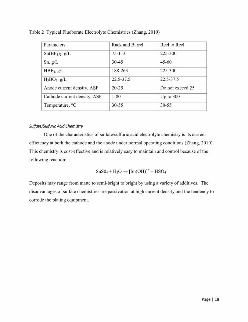
Fluoborate Chemistry
Fluoborate chemistry is one of the oldest electroplating acid tin chemistries and is
typically used in high-speed plating (Zhang, 2010). Organic additives most commonly used in
fluoborate chemistry are peptone, gelatin, β-naphthol, catechol, and hydroquinone. Typical bath
compositions are listed below, and when these compounds are added the result is a fine, smooth
deposit. The advantages of fluoborate chemistry are its ability to operate at high current densities
and its high throwing power and high current efficiency at both the anode and cathode. The
major disadvantage of fluoborate chemistry is the environmental concerns associated with the
fluoride and boric ions.
Page | 18
Table 2 Typical Fluoborate Electrolyte Chemistries (Zhang, 2010)
Parameters Rack and Barrel Reel to Reel
Sn(BF4)2, g/L 75-113 225-300
Sn, g/L 30-45 45-60
HBF4, g/L 188-263 225-300
H3BO3, g/L 22.5-37.5 22.5-37.5
Anode current density, ASF 20-25 Do not exceed 25
Cathode current density, ASF 1-80 Up to 300
Temperature, °C 30-55 30-55
Sulfate/Sulfuric Acid Chemistry
One of the characteristics of sulfate/sulfuric acid electrolyte chemistry is its current
efficiency at both the cathode and the anode under normal operating conditions (Zhang, 2010).
This chemistry is cost-effective and is relatively easy to maintain and control because of the
following reaction:
SnS04 + H2O → [Sn(OH)]+ + HSO4
-
Deposits may range from matte to semi-bright to bright by using a variety of additives. The
disadvantages of sulfate chemistries are passivation at high current density and the tendency to
corrode the plating equipment.
Page | 19
Table 3 Typical Sulfate/Sulfuric Acid Electrolyte Chemistries (Zhang, 2010)
Parameters Range
SnSO4, g/L 15-45
Sn, g/L 7.5-22.5
Sulfuric acid, g/L 135-210
Additives Alkylphenol, imidazonline,
heterocyclic aldehydes
Anodes Pure Sn
Anode current density, ASF 25 max
Cathode current density, ASF 1-25
Temperature Room Temperature
Agitation Mechanical, cathode rod
Phenolsulfonic Acid and Halogen Electrolytes
Phenolsulfonic acid and halogen electrolytes are the two most commonly used
chemistries to plate pure tin in the continuous steel strip plating industry (Zhang, 2010). Typical
formulations and operating conditions are shown below.
Table 4 Typical Phenolsulfonic Acid Electrokyte Chemistries (Zhang, 2010)
Parameters Range
Sn, g/L 20-35
Phenolsulfonic acid,
g/L
40-80
Additives Ethoylated β-naphtholsulfonic
acid
Antioxidant -
Current Density, ASF 200-500
Temperature, °C 30-40
Page | 20
Table 5 Typical Halogen Electrolyte Chemistry (Zhang, 2010)
Parameters Range
NaF, g/L 30
NaHF2, g/L 31
SnF2, g/L 19
SnCl2˖5H2O, g/L 22
Na2Fe(CN)6˖10H2O,
g/L
2-4
Additives Naphtholsulfonic acid and polyalkyelen
oxides
Antioxidant Ρ-NH2C6H4NHCOMe
pH 3-4
Current density, ASF 200-500
Temperature, °C 55-65
The benefit of either of these processes is their ability to operate at very high current densities,
which is an advantage in the steel industry. Phenolsulfonic acid processes use a vertical cell
design with either a soluble or insoluble anode, whereas the halogen process uses a horizontal
cell design with a soluble anode. Both processes, however, cause sludge formation and
environmental issues have brought about the development of an alternative methanesulfonic
acid-based process that is more environmentally benign.
Methanesulfonic Acid Electrolyte
Proell recognized the electroplating applications of methanesulfonic acid as an electrolyte
in the 1940s, although it was not readily accepted until the early 1980s. Methanesulfonic
chemistry has shown clear advantages over the previously described electrolytes using
fluoborate, sulfate, halogen, and phenolsulfonic acids. The conversion from Sn (II) to Sn (IV) is
less of a problem than for fluoborate/sulfate chemistries and is less costly than the previously
described fluoborate, PSA, and halogen chemistries.
Page | 21
Research by Ivey et al
Ivey et al. have been working on electrodeposition of the Au-Sn system for packaging
microelectronics and optoelectronic devices. Currently, Ivey et al. has developed methods for
co-deposition and sequential deposition of Au-rich, Au-Sn solders on both patterned and un-
patterned substrates. Co-deposition studies were completed using a non-cyanide based
electrolyte containing five major components: KAuCl4, SnCl2˖2H20, tribasic ammonium citrate
(NH4)3HC6H5O7, sodium sulfite (Na2SO3), and ascorbic acid (C6H8O6). Sequential deposition
studies were completed using separate and simple Au and Sn electrolytes. The Au electrolyte
contained (NH4)3HC6H5O7, KAuCl4, and Na2SO3, whereas the Sn electrolyte contained
(NH4)3HC6H5O7and SnCl2∙2H2O.
Sun and Ivey (1999) initially investigated the electrolyte chemistry used for co-deposition
of Au-Sn solders and their investigation led to the development of the co-deposition electrolyte
mentioned above. They determined that the Au-Sn plating bath stability depended on the total
Au and Sn content, additive content, and how the electrolyte was prepared and stored. The
resulting deposits were compared using pulse current and direct current plating techniques,
demonstrating that a pulse current using a duty cycle of 20% produced finer and smoother
microstructures (Sun and Ivey, 2001).
Doesburg and Ivey (2000) continued to study the co-deposition of the Au-Sn system
using the electrolyte developed by Sun and Ivey. They studied the effects of average current
density on the microstructure and preferred orientation of the deposit. The preferred orientation
was related not only to the microstructure produced but also to the phase or phases that were
present in the deposit. The average current density used controlled the phases formed during
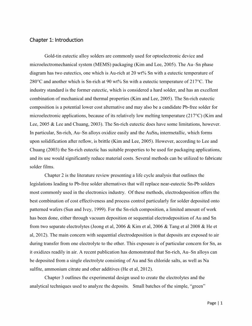
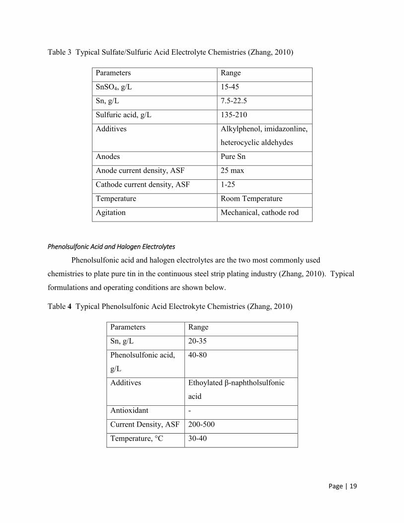
electrodeposition. Djurfors and Ivey (2002) showed that changes in average current density
could produce multilayered deposits with multiple phases present in the solder structure. This
multilayer structure created was composed of two stoichiometric phases: AuSn and Au5Sn
(Figure 4).
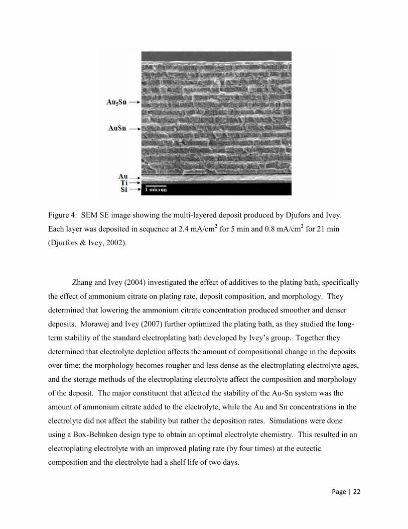
Page | 22
Figure 4: SEM SE image showing the multi-layered deposit produced by Djufors and Ivey.
Each layer was deposited in sequence at 2.4 mA/cm2 for 5 min and 0.8 mA/cm
2 for 21 min
(Djurfors & Ivey, 2002).
Zhang and Ivey (2004) investigated the effect of additives to the plating bath, specifically
the effect of ammonium citrate on plating rate, deposit composition, and morphology. They
determined that lowering the ammonium citrate concentration produced smoother and denser
deposits. Morawej and Ivey (2007) further optimized the plating bath, as they studied the long-
term stability of the standard electroplating bath developed by Ivey’s group. Together they
determined that electrolyte depletion affects the amount of compositional change in the deposits
over time; the morphology becomes rougher and less dense as the electroplating electrolyte ages,
and the storage methods of the electroplating electrolyte affect the composition and morphology
of the deposit. The major constituent that affected the stability of the Au-Sn system was the
amount of ammonium citrate added to the electrolyte, while the Au and Sn concentrations in the
electrolyte did not affect the stability but rather the deposition rates. Simulations were done
using a Box-Behnken design type to obtain an optimal electrolyte chemistry. This resulted in an
electroplating electrolyte with an improved plating rate (by four times) at the eutectic
composition and the electrolyte had a shelf life of two days.
Page | 23
Tang and Ivey (2008) investigated the effects of sequential electrodeposition on the Au-
Sn system using the standard electroplating bath electrolyte described earlier. Sequential
deposition in comparison with co-deposition can be an advantageous process method. A key
difference between the two methods is the difference in the stability of the electroplating
electrolyte. The co-deposition electrolyte has a shelf life of three days, while the separate Au
and Sn electrolytes have shelf lives of at least three months. As such, sequential
electrodeposition of the Au-Sn system maybe a more cost-effective method and may be easier to
implement and control for commercial processes. Tang and Ivey (2008) also investigated the
effects of deposition order and the resulting microstructures of Au-rich and Sn-rich, Au-Sn
solders alloys. Tang et al. (2008) studied the room temperature interface reactions of
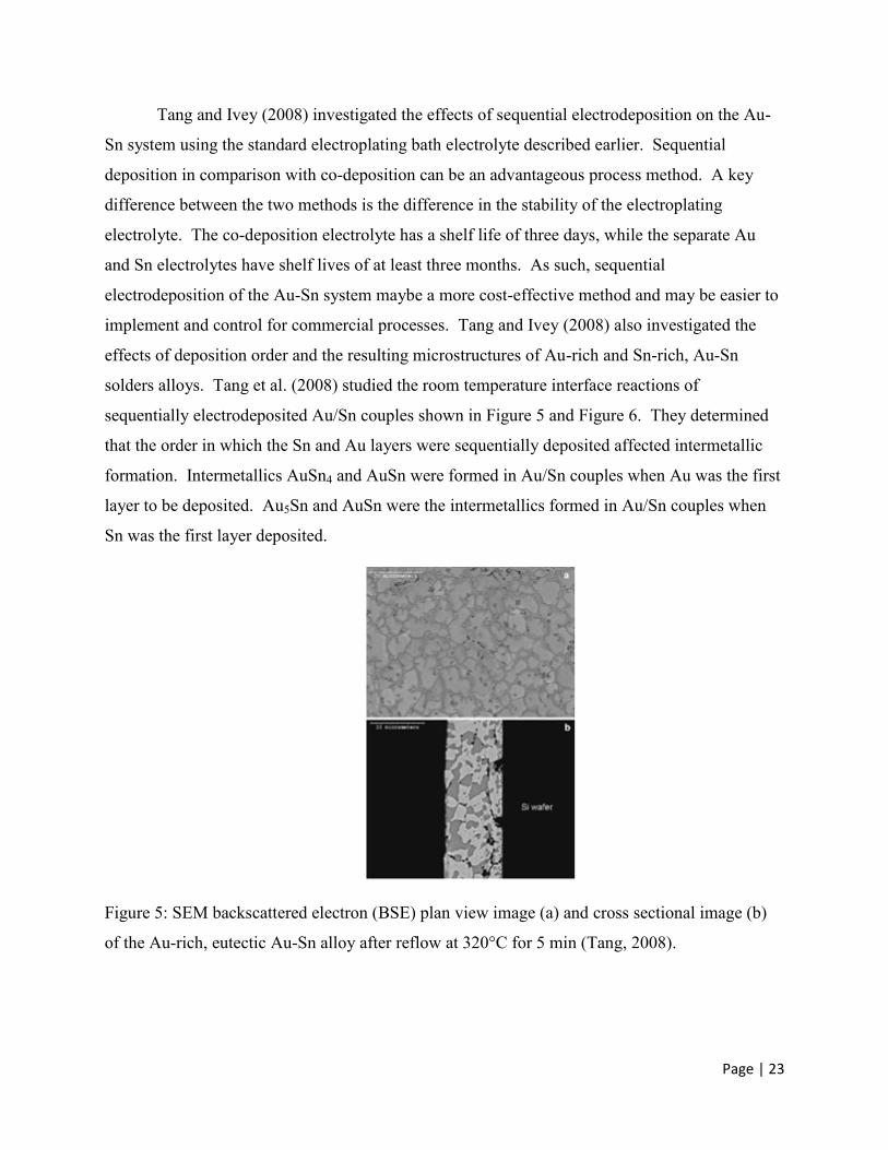
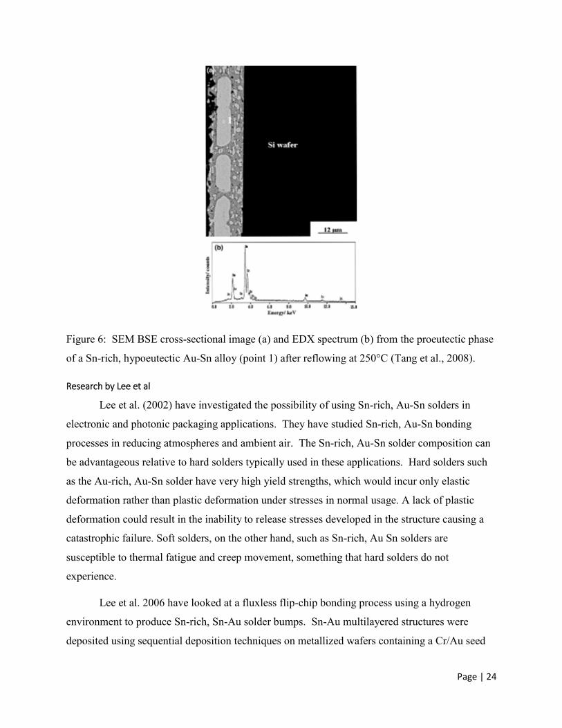
sequentially electrodeposited Au/Sn couples shown in Figure 5 and Figure 6. They determined
that the order in which the Sn and Au layers were sequentially deposited affected intermetallic
formation. Intermetallics AuSn4 and AuSn were formed in Au/Sn couples when Au was the first
layer to be deposited. Au5Sn and AuSn were the intermetallics formed in Au/Sn couples when
Sn was the first layer deposited.
Figure 5: SEM backscattered electron (BSE) plan view image (a) and cross sectional image (b)
of the Au-rich, eutectic Au-Sn alloy after reflow at 320°C for 5 min (Tang, 2008).
Page | 24
Figure 6: SEM BSE cross-sectional image (a) and EDX spectrum (b) from the proeutectic phase
of a Sn-rich, hypoeutectic Au-Sn alloy (point 1) after reflowing at 250°C (Tang et al., 2008).
Research by Lee et al
Lee et al. (2002) have investigated the possibility of using Sn-rich, Au-Sn solders in
electronic and photonic packaging applications. They have studied Sn-rich, Au-Sn bonding
processes in reducing atmospheres and ambient air. The Sn-rich, Au-Sn solder composition can
be advantageous relative to hard solders typically used in these applications. Hard solders such
as the Au-rich, Au-Sn solder have very high yield strengths, which would incur only elastic
deformation rather than plastic deformation under stresses in normal usage. A lack of plastic
deformation could result in the inability to release stresses developed in the structure causing a
catastrophic failure. Soft solders, on the other hand, such as Sn-rich, Au Sn solders are
susceptible to thermal fatigue and creep movement, something that hard solders do not
experience.
Lee et al. 2006 have looked at a fluxless flip-chip bonding process using a hydrogen
environment to produce Sn-rich, Sn-Au solder bumps. Sn-Au multilayered structures were
deposited using sequential deposition techniques on metallized wafers containing a Cr/Au seed
Page | 25
layer. A Sn layer was deposited first followed by an Au layer to prevent Sn oxidation. The Sn
layer was deposited using a stannous Sn-based electrolyte with a bath temperature of 46°C and a
pH of 1. A current density of 21.5 mA/cm2 was used for 85 min to produce a 40 µm layer of Sn.
The gold was deposited directly after tin deposition. The Au electrolyte was a neutral non-
cyanide electrolyte and Au was deposited at 60°C with a current density of 4.6 mA/cm2.
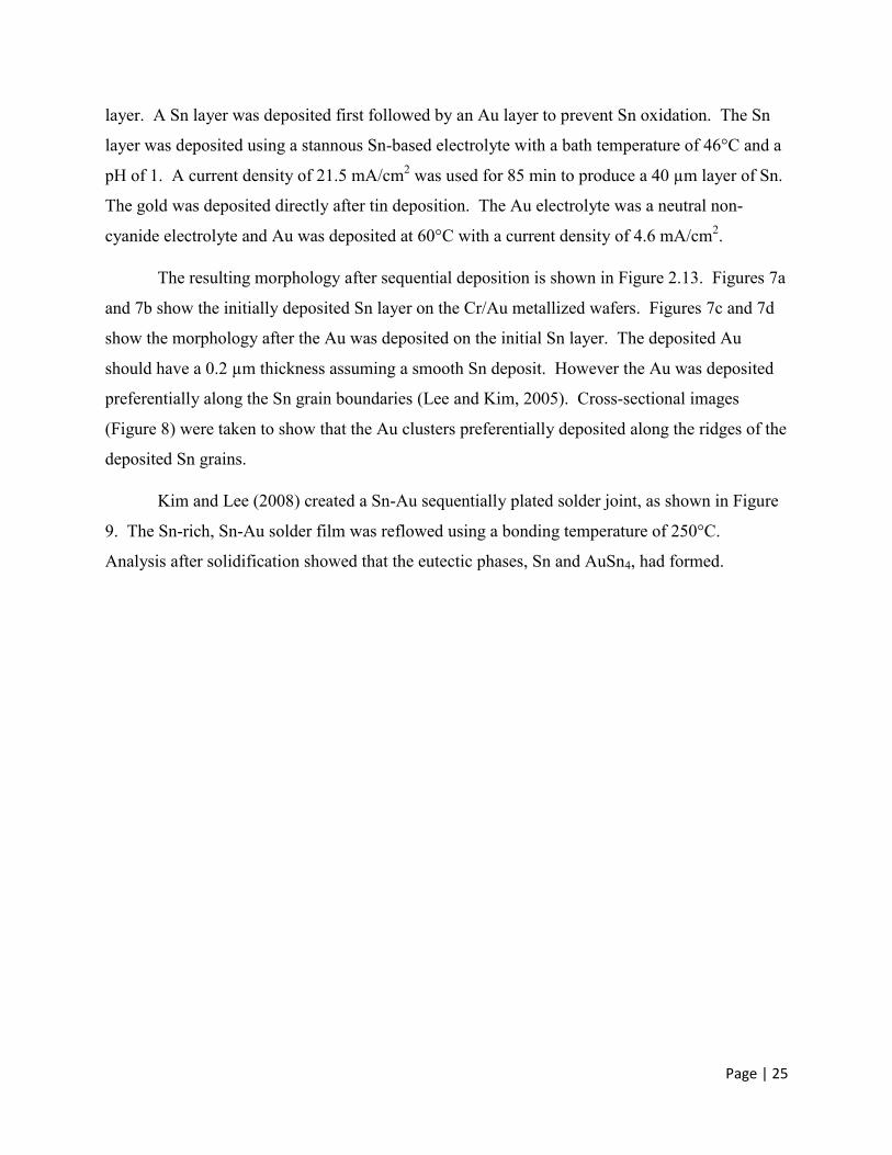
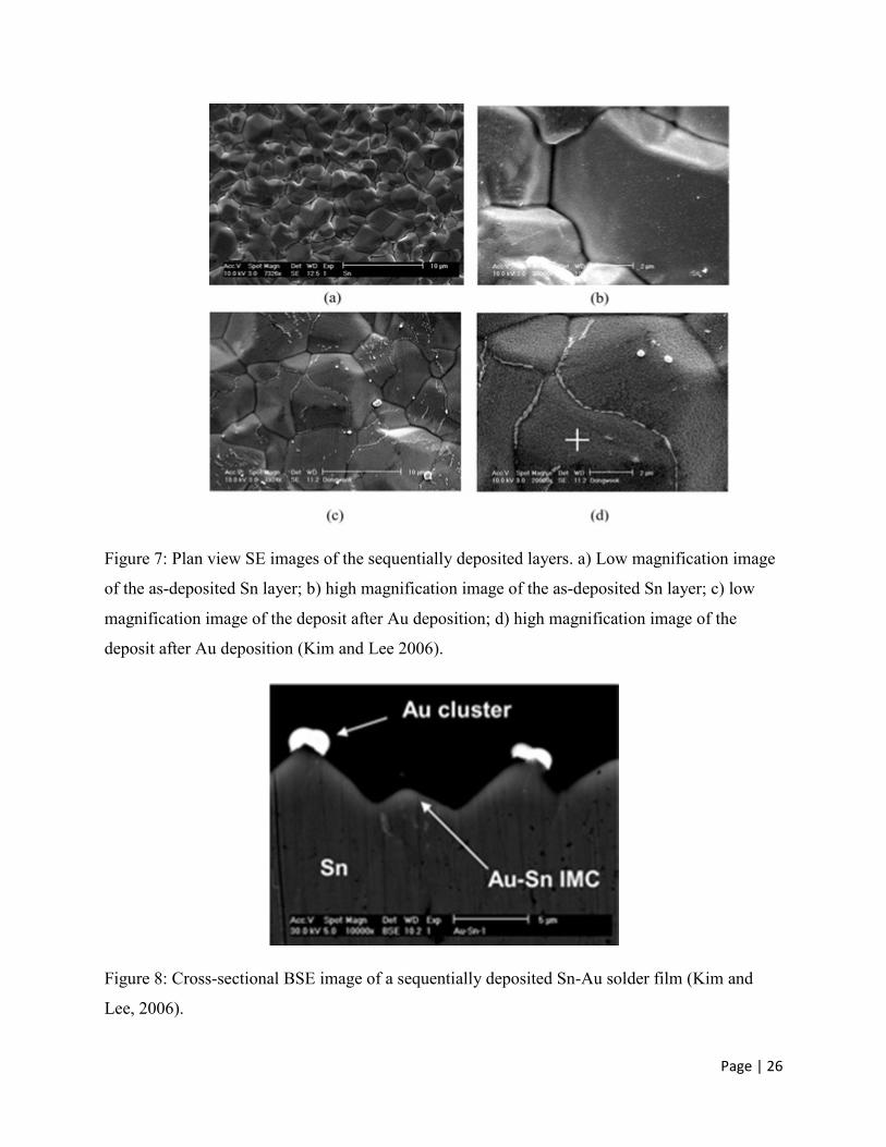
The resulting morphology after sequential deposition is shown in Figure 2.13. Figures 7a
and 7b show the initially deposited Sn layer on the Cr/Au metallized wafers. Figures 7c and 7d
show the morphology after the Au was deposited on the initial Sn layer. The deposited Au
should have a 0.2 µm thickness assuming a smooth Sn deposit. However the Au was deposited
preferentially along the Sn grain boundaries (Lee and Kim, 2005). Cross-sectional images
(Figure 8) were taken to show that the Au clusters preferentially deposited along the ridges of the
deposited Sn grains.
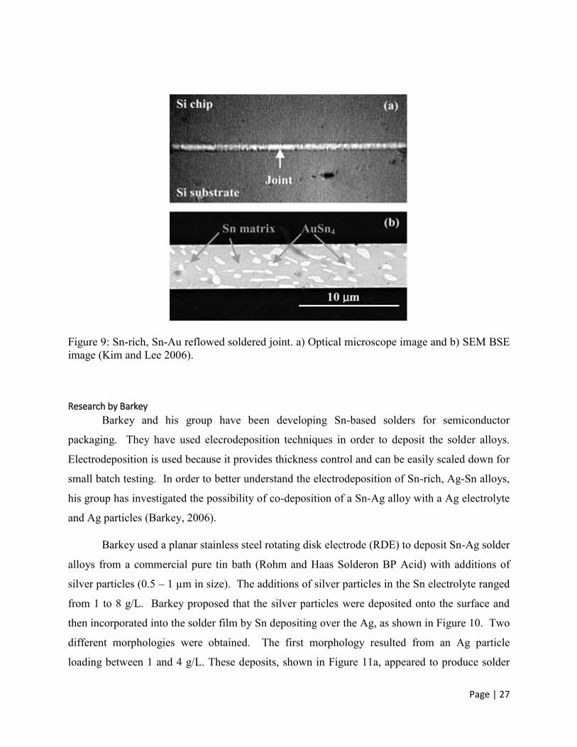
Kim and Lee (2008) created a Sn-Au sequentially plated solder joint, as shown in Figure
9. The Sn-rich, Sn-Au solder film was reflowed using a bonding temperature of 250°C.
Analysis after solidification showed that the eutectic phases, Sn and AuSn4, had formed.
Page | 26
Figure 7: Plan view SE images of the sequentially deposited layers. a) Low magnification image
of the as-deposited Sn layer; b) high magnification image of the as-deposited Sn layer; c) low
magnification image of the deposit after Au deposition; d) high magnification image of the
deposit after Au deposition (Kim and Lee 2006).
Figure 8: Cross-sectional BSE image of a sequentially deposited Sn-Au solder film (Kim and
Lee, 2006).
Page | 27
Figure 9: Sn-rich, Sn-Au reflowed soldered joint. a) Optical microscope image and b) SEM BSE
image (Kim and Lee 2006).
Research by Barkey
Barkey and his group have been developing Sn-based solders for semiconductor
packaging. They have used elecrodeposition techniques in order to deposit the solder alloys.
Electrodeposition is used because it provides thickness control and can be easily scaled down for
small batch testing. In order to better understand the electrodeposition of Sn-rich, Ag-Sn alloys,
his group has investigated the possibility of co-deposition of a Sn-Ag alloy with a Ag electrolyte
and Ag particles (Barkey, 2006).
Barkey used a planar stainless steel rotating disk electrode (RDE) to deposit Sn-Ag solder
alloys from a commercial pure tin bath (Rohm and Haas Solderon BP Acid) with additions of
silver particles (0.5 – 1 µm in size). The additions of silver particles in the Sn electrolyte ranged
from 1 to 8 g/L. Barkey proposed that the silver particles were deposited onto the surface and
then incorporated into the solder film by Sn depositing over the Ag, as shown in Figure 10. Two
different morphologies were obtained. The first morphology resulted from an Ag particle
loading between 1 and 4 g/L. These deposits, shown in Figure 11a, appeared to produce solder
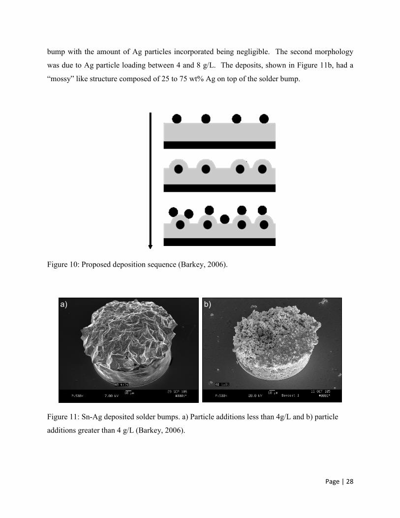
Page | 28
bump with the amount of Ag particles incorporated being negligible. The second morphology
was due to Ag particle loading between 4 and 8 g/L. The deposits, shown in Figure 11b, had a
“mossy” like structure composed of 25 to 75 wt% Ag on top of the solder bump.
Figure 10: Proposed deposition sequence (Barkey, 2006).
Figure 11: Sn-Ag deposited solder bumps. a) Particle additions less than 4g/L and b) particle
additions greater than 4 g/L (Barkey, 2006).
a) b)
Page | 29
Applications
With the directive of reducing and eliminating Pb-based solders, Pb-free solders have
been used in commercial grade electronic and white goods. As technologies improve and
packaging architectures become more advanced, there are increases in the demands for electronic
manufacturing. Understanding the drivers for change in electronic architectures creates an
opportunity to explore the materials science of soldering (Evans, 2007).
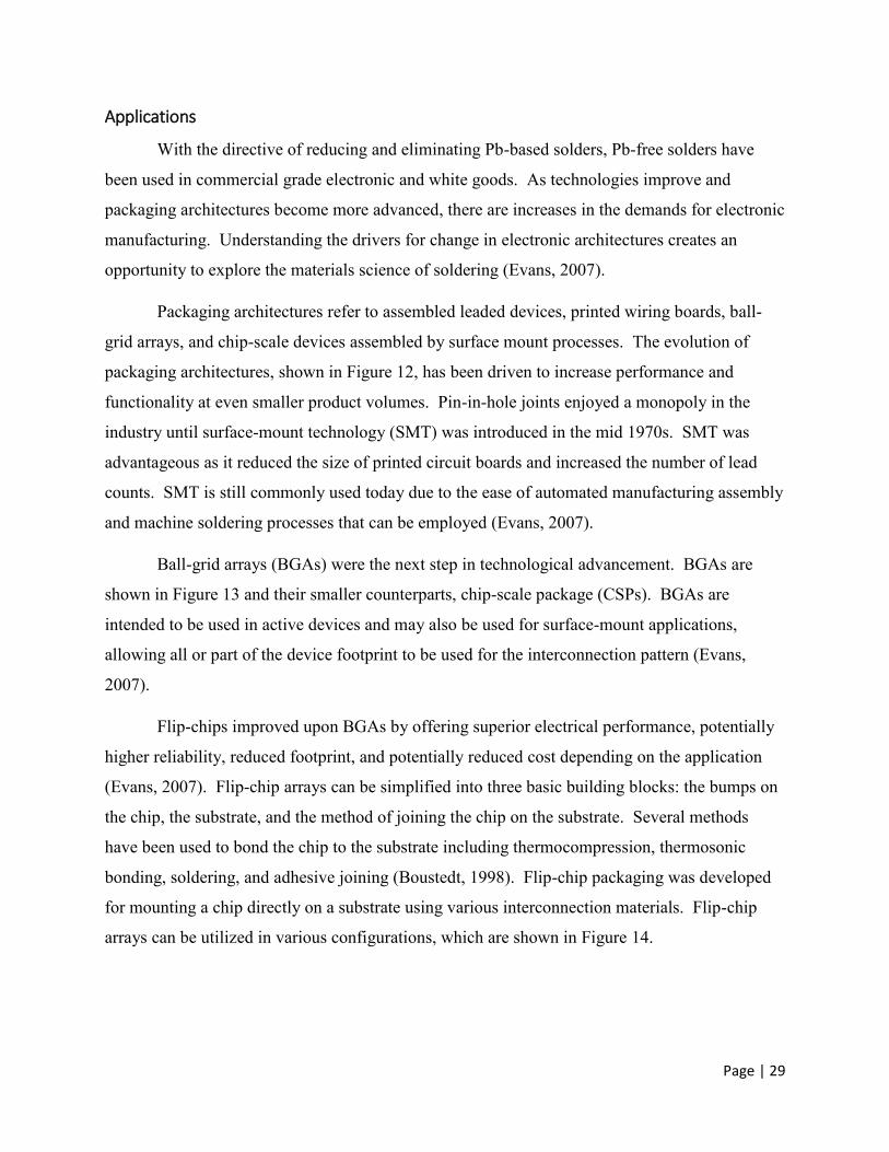
Packaging architectures refer to assembled leaded devices, printed wiring boards, ball-
grid arrays, and chip-scale devices assembled by surface mount processes. The evolution of
packaging architectures, shown in Figure 12, has been driven to increase performance and
functionality at even smaller product volumes. Pin-in-hole joints enjoyed a monopoly in the
industry until surface-mount technology (SMT) was introduced in the mid 1970s. SMT was
advantageous as it reduced the size of printed circuit boards and increased the number of lead
counts. SMT is still commonly used today due to the ease of automated manufacturing assembly
and machine soldering processes that can be employed (Evans, 2007).
Ball-grid arrays (BGAs) were the next step in technological advancement. BGAs are
shown in Figure 13 and their smaller counterparts, chip-scale package (CSPs). BGAs are
intended to be used in active devices and may also be used for surface-mount applications,
allowing all or part of the device footprint to be used for the interconnection pattern (Evans,
2007).
Flip-chips improved upon BGAs by offering superior electrical performance, potentially
higher reliability, reduced footprint, and potentially reduced cost depending on the application
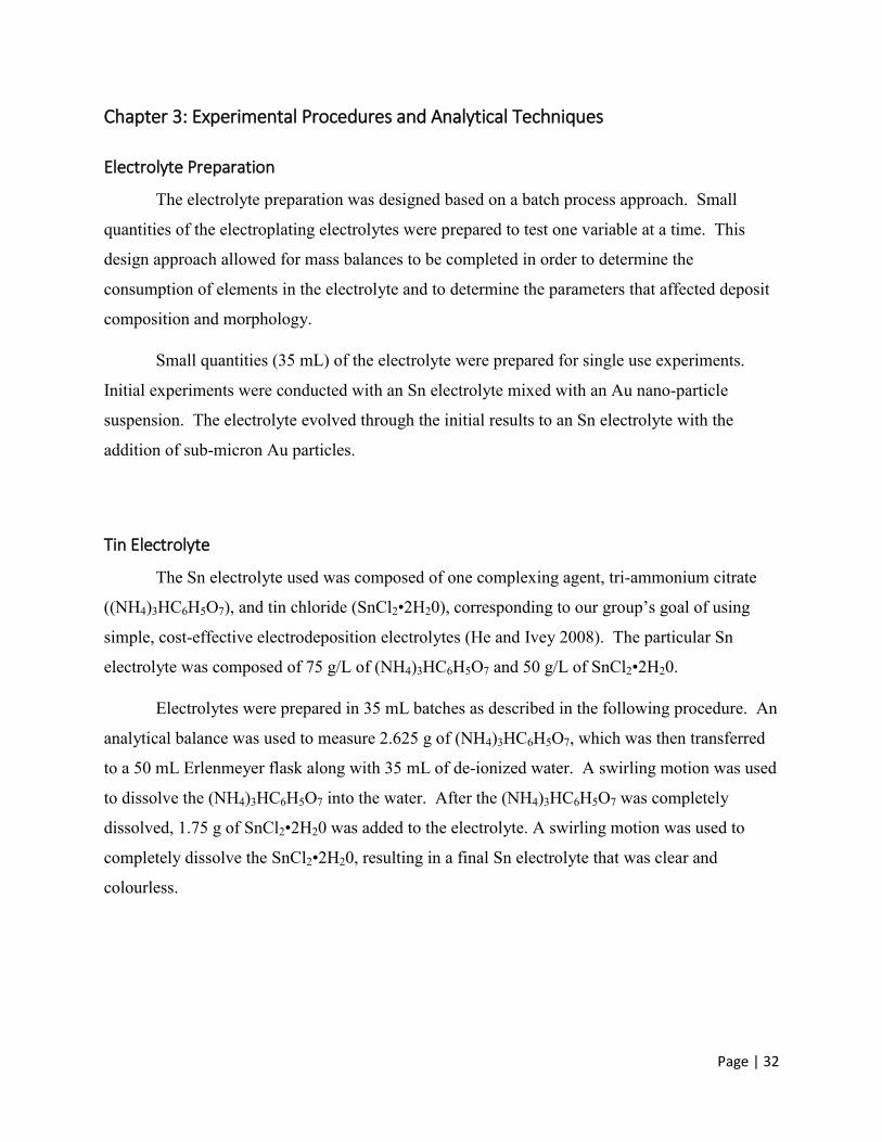
(Evans, 2007). Flip-chip arrays can be simplified into three basic building blocks: the bumps on
the chip, the substrate, and the method of joining the chip on the substrate. Several methods
have been used to bond the chip to the substrate including thermocompression, thermosonic
bonding, soldering, and adhesive joining (Boustedt, 1998). Flip-chip packaging was developed
for mounting a chip directly on a substrate using various interconnection materials. Flip-chip
arrays can be utilized in various configurations, which are shown in Figure 14.
Page | 30
Figure 12: Development of solder joints in relation to packaging architectures (Evans, 2007).
Page | 31
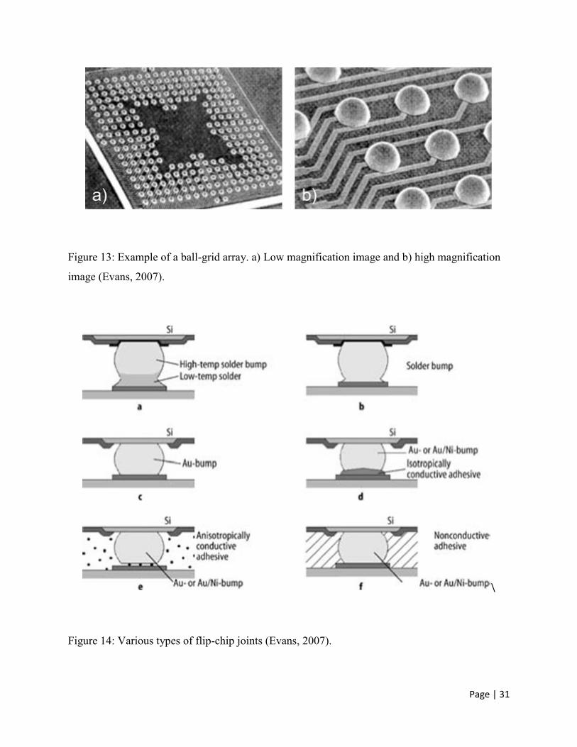
Figure 13: Example of a ball-grid array. a) Low magnification image and b) high magnification
image (Evans, 2007).
\
Figure 14: Various types of flip-chip joints (Evans, 2007).
Page | 32
Chapter 3: Experimental Procedures and Analytical Techniques
Electrolyte Preparation
The electrolyte preparation was designed based on a batch process approach. Small
quantities of the electroplating electrolytes were prepared to test one variable at a time. This
design approach allowed for mass balances to be completed in order to determine the
consumption of elements in the electrolyte and to determine the parameters that affected deposit
composition and morphology.
Small quantities (35 mL) of the electrolyte were prepared for single use experiments.
Initial experiments were conducted with an Sn electrolyte mixed with an Au nano-particle
suspension. The electrolyte evolved through the initial results to an Sn electrolyte with the
addition of sub-micron Au particles.
Tin Electrolyte
The Sn electrolyte used was composed of one complexing agent, tri-ammonium citrate
((NH4)3HC6H5O7), and tin chloride (SnCl2•2H20), corresponding to our group’s goal of using
simple, cost-effective electrodeposition electrolytes (He and Ivey 2008). The particular Sn
electrolyte was composed of 75 g/L of (NH4)3HC6H5O7 and 50 g/L of SnCl2•2H20.
Electrolytes were prepared in 35 mL batches as described in the following procedure. An
analytical balance was used to measure 2.625 g of (NH4)3HC6H5O7, which was then transferred
to a 50 mL Erlenmeyer flask along with 35 mL of de-ionized water. A swirling motion was used
to dissolve the (NH4)3HC6H5O7 into the water. After the (NH4)3HC6H5O7 was completely
dissolved, 1.75 g of SnCl2•2H20 was added to the electrolyte. A swirling motion was used to
completely dissolve the SnCl2•2H20, resulting in a final Sn electrolyte that was clear and
colourless.
Page | 33
Gold Nano-particle Suspension
A stock suspension of Au nano-particles was prepared following the procedure described
by McFarland et al. (2004). Initially, an electrolyte containing 1.0 mM HAuCl4 was made by
dissolving 0.1 g of the salt into 500 mL of distilled water. A second separate electrolyte
containing 38.8 mM sodium citrate (Na3C6H5O7) was then prepared by adding 0.5 g of sodium
citrate into 50 mL of distilled water (McFarland et al., 2004). The Au nano-particle suspension
was prepared by placing 500 mL of the 1.0 mM HAuCl4 stock electrolyte on a hot plate while a
magnetic stir bar agitated the solution. After the solution began to boil, the 38.8 mM sodium
citrate solution was slowly added to the HAuCl4 solution using an eyedropper. The solution was
maintained at a volume of 500 mL by adding de-ionized water. The Au nano-particle suspension
was completed when the solution became deep red in colour. The suspension was then allowed
to cool to room temperature before use.
Gold Nano-particle Electrolyte
In order to create Sn-rich, Sn-Au solder films, SnCl2•2H20 and (NH4)3HC6H5O7 were
added directly into the Au nano-particle suspension described in the previous section. However,
with the addition of SnCl2•2H20 and (NH4)3HC6H5O7, the Au nano-particles were no longer
stable in solution. The Au nano-particles were only able to remain in suspension (without tin
chloride or citrate additions) because the citrate anions covered the surface of the Au nano-
particles, as shown schematically in Figure 15. The citrate anions interacted with the Au nano-
particles through an adsorption interaction which created an electrostatic repulsion that prevented
the Au nano-particles from agglomerating and settling out of electrolyte (McFarland et al.,
2004). When a strong electrolyte is added, the citrate layer can be stripped off causing the
repulsive force between the particles to be eliminated (McFarland et al., 2004). As there is no
longer a repulsive force between the Au particles, they will aggregate. Evidence of this
phenomenon occurred when the SnCl2•2H20 and (NH4)3HC6H5O7 were directly added to the
suspension.
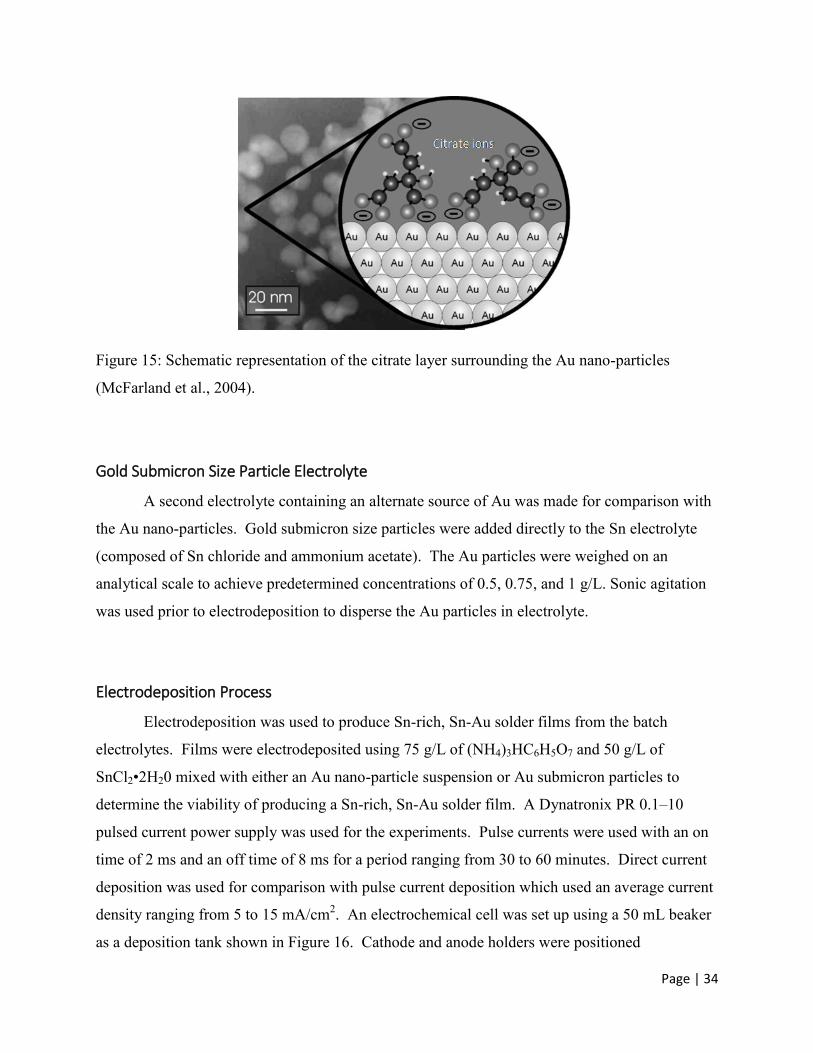
Page | 34
Figure 15: Schematic representation of the citrate layer surrounding the Au nano-particles
(McFarland et al., 2004).
Gold Submicron Size Particle Electrolyte
A second electrolyte containing an alternate source of Au was made for comparison with
the Au nano-particles. Gold submicron size particles were added directly to the Sn electrolyte
(composed of Sn chloride and ammonium acetate). The Au particles were weighed on an
analytical scale to achieve predetermined concentrations of 0.5, 0.75, and 1 g/L. Sonic agitation
was used prior to electrodeposition to disperse the Au particles in electrolyte.
Electrodeposition Process
Electrodeposition was used to produce Sn-rich, Sn-Au solder films from the batch
electrolytes. Films were electrodeposited using 75 g/L of (NH4)3HC6H5O7 and 50 g/L of
SnCl2•2H20 mixed with either an Au nano-particle suspension or Au submicron particles to
determine the viability of producing a Sn-rich, Sn-Au solder film. A Dynatronix PR 0.1–10
pulsed current power supply was used for the experiments. Pulse currents were used with an on
time of 2 ms and an off time of 8 ms for a period ranging from 30 to 60 minutes. Direct current
deposition was used for comparison with pulse current deposition which used an average current
density ranging from 5 to 15 mA/cm2. An electrochemical cell was set up using a 50 mL beaker
as a deposition tank shown in Figure 16. Cathode and anode holders were positioned
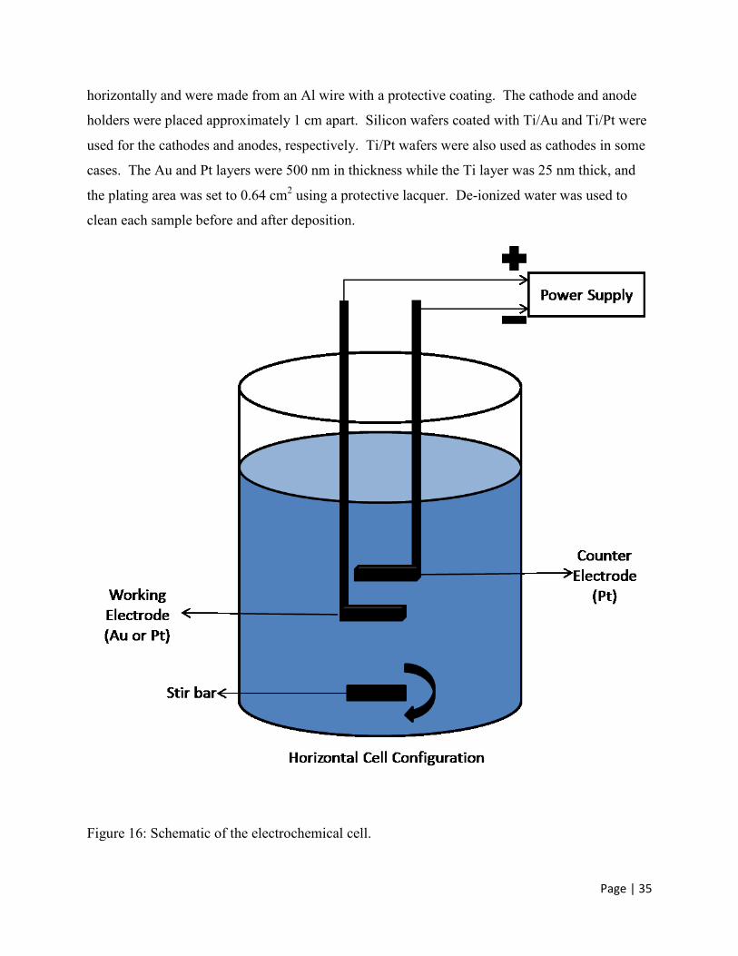
Page | 35
horizontally and were made from an Al wire with a protective coating. The cathode and anode
holders were placed approximately 1 cm apart. Silicon wafers coated with Ti/Au and Ti/Pt were
used for the cathodes and anodes, respectively. Ti/Pt wafers were also used as cathodes in some
cases. The Au and Pt layers were 500 nm in thickness while the Ti layer was 25 nm thick, and
the plating area was set to 0.64 cm2 using a protective lacquer. De-ionized water was used to
clean each sample before and after deposition.
Figure 16: Schematic of the electrochemical cell.
Page | 36
Analytical Techniques
Sample Preparation for Scanning Electron Microscopy (SEM)
Deposits created using the electrodeposition process were prepared for inspection of their
morphology and composition. Plan view and cross-sections of the deposits were prepared for
analysis. Samples were initially cleaved to create two samples of a single deposit for analysis.
One sample was used for plan-view analysis to determine deposit composition and morphology,
while the other half was mounted in an epoxy mold for cross-sectional analysis. Cross-sectional
samples were prepared using 320 and 600 grit SiC paper and a 0.05 µm alumina suspension to
remove any cleaving artifacts. Copper tape was used to ground the samples and to prevent
charging effects during SEM annalysis.
Scanning Electron Microscopy (SEM)
A scanning electron microscope has two major components: the electron column and the
control console. The electron column is composed of an electron gun and two or more lenses
(Goldstein et al., 2003). The electron gun can generate and accelerate electrons with an energy
range of 0.1–30 keV producing a spot size of less than 10 nm, which interacts with the specimen
to a depth of approximately 1 µm (Goldstein et al., 2003). The lenses influence the path of the
highly excited electrons traveling down the electron column. A control console consists of a
viewing screen and controls used to adjust the electron beam, lenses, and image quality.
A Hitachi S2700 SEM was used to examine the electrodeposited samples. Images of the
surfaces (i.e., plan-view samples) and cross sections were taken. Area and point composition
analyses using energy dispersive x-ray spectroscopy (EDS) were also conducted. The following
sections describe the procedure taken to obtain secondary electron (SE) images, backscattered
electron (BSE) images, and EDS analysis.
Secondary Electron (SE) and Backscattered Electron (BSE) Imaging
The Hitachi S2700 SEM was equipped with a positively biased Everhart-Thornley (E-T)
detector and a GW Electronics System was used to collect SE and BSE, respectively, for
imaging. The SEs and BSEs have different energies and are produced via different mechanisms.
Different information can be extracted by analyzing both SE and BSE images. SE images are
Page | 37
susceptible to changes in topography. BSE images are primarily dependent on the atomic
number of the elements present in the sample and create contrast within the image. The E-T
detector was used to obtain SE images of both plan-view and cross-sectional samples. The GW
Electronics System is a solid-state detector divided into four quadrants to collect BSEs for
imaging.
Energy Dispersive X-Ray Spectroscopy (EDS)
An x-ray detector attached to the Hitachi S2700 SEM was used to detect x-rays for EDS
analysis. The specific x-ray detector used was a Prism Intrinsic Germanium (IG) semiconductor.
An accelerating voltage of 20 kV at a working distance of 17 mm was utilized and the probe
current was increased to obtain a count rate ranging from 2000–3500 counts/seconds. The
working distance and aperture size were set to 17 mm and 50 µm, respectively. The x-ray
collection time was set to 90 seconds.
Pure Au and Sn standards were used for quantitative analysis to determine the
composition of the electroplated films. To determine the overall composition for each sample,
three areas 200 µm by 200 µm were selected and analyzed. The average composition was
reported in the results along with one standard deviation. In some cases, point analysis was
done.
Secondary Analytical Techniques
Secondary analytical techniques were used to confirm the chemical composition and size
of the nano-Au particles and submicron Au particles. This section provides brief descriptions of
Zeta potential, x-ray photoelectron spectroscopy (XPS), and transmission electron microscopy
(TEM) analysis.
Zeta Potential
Zeta potential was used as a verification technique to confirm the size of the Au nano-
particles in suspension. The majority of the macroscopic materials or particulates that come into
contact with a liquid will acquire an electronic charge on their surfaces. Zeta potential can be
used as an indicator of this charge. Moreover, zeta potential can be used to predict and control
the stability of colloidal suspensions/emulsions or as a controlling parameter in processes such as
Page | 38
adhesion, surface coating, filtration, lubrication, and corrosion. A ZetaPlus zeta potential
analyzer from Brookhaven Instruments Corp. was used to measure the diameter of the Au nano-
particles. The ZetaPlus system used software that measured the particle size by dynamic light
scattering (www.brookhaven.co.uk).
X-ray Photoelectron Spectroscopy (XPS)
XPS is primarily a surface analysis technique that gathers information 0.5–2.5 nm from
the surface (Goldstein et al., 2003). In XPS, electrons are ejected from their localized core levels
by photon energy. A plot of photoelectron flux against measured kinetic energy can be created,
revealing a series of peaks corresponding to the orbital structure of the atom (Goldstein et al.,
2003). XPS was carried out with a Kratos AXIS 165 XPS system using a monochromatic Al Kα
source and a current of 15 mA.
Transmission Electron Microscopy (TEM)
Transmission electron microscopy was used as a secondary verification method for the
nano-Au particles. TEM samples were prepared by placing droplets of the nano-Au particle
suspension onto a carbon grid and allowing the water to evaporate. TEM images are produced
using a beam of highly energized electrons that are guided by a series of electromagnetic lenses
under a vacuum. The beam of electrons then passes through the sample creating an image on a
fluorescent screen. Electron diffraction patterns and bright field images of the nano-Au particles
were taken using a JEOL-2010 TEM.
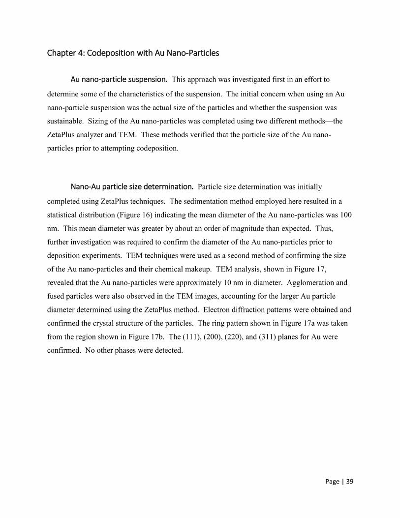
Page | 39
Chapter 4: Codeposition with Au Nano-Particles
Au nano-particle suspension. This approach was investigated first in an effort to
determine some of the characteristics of the suspension. The initial concern when using an Au
nano-particle suspension was the actual size of the particles and whether the suspension was
sustainable. Sizing of the Au nano-particles was completed using two different methods—the
ZetaPlus analyzer and TEM. These methods verified that the particle size of the Au nano-
particles prior to attempting codeposition.
Nano-Au particle size determination. Particle size determination was initially
completed using ZetaPlus techniques. The sedimentation method employed here resulted in a
statistical distribution (Figure 16) indicating the mean diameter of the Au nano-particles was 100
nm. This mean diameter was greater by about an order of magnitude than expected. Thus,
further investigation was required to confirm the diameter of the Au nano-particles prior to
deposition experiments. TEM techniques were used as a second method of confirming the size
of the Au nano-particles and their chemical makeup. TEM analysis, shown in Figure 17,
revealed that the Au nano-particles were approximately 10 nm in diameter. Agglomeration and
fused particles were also observed in the TEM images, accounting for the larger Au particle
diameter determined using the ZetaPlus method. Electron diffraction patterns were obtained and
confirmed the crystal structure of the particles. The ring pattern shown in Figure 17a was taken
from the region shown in Figure 17b. The (111), (200), (220), and (311) planes for Au were
confirmed. No other phases were detected.
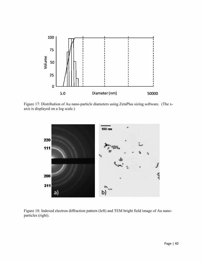
Page | 40
Figure 17: Distribution of Au nano-particle diameters using ZetaPlus sizing software. (The x-
axis is displayed on a log scale.)
Figure 18: Indexed electron diffraction pattern (left) and TEM bright field image of Au nano-
particles (right).
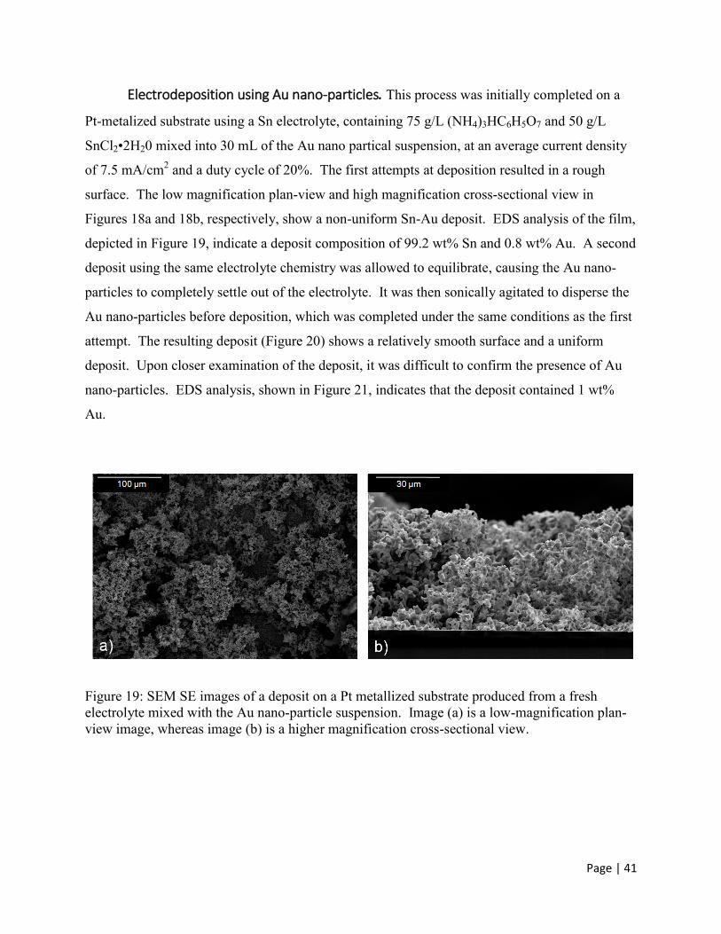
Page | 41
Electrodeposition using Au nano-particles. This process was initially completed on a
Pt-metalized substrate using a Sn electrolyte, containing 75 g/L (NH4)3HC6H5O7 and 50 g/L
SnCl2•2H20 mixed into 30 mL of the Au nano partical suspension, at an average current density
of 7.5 mA/cm2 and a duty cycle of 20%. The first attempts at deposition resulted in a rough
surface. The low magnification plan-view and high magnification cross-sectional view in
Figures 18a and 18b, respectively, show a non-uniform Sn-Au deposit. EDS analysis of the film,
depicted in Figure 19, indicate a deposit composition of 99.2 wt% Sn and 0.8 wt% Au. A second
deposit using the same electrolyte chemistry was allowed to equilibrate, causing the Au nano-
particles to completely settle out of the electrolyte. It was then sonically agitated to disperse the
Au nano-particles before deposition, which was completed under the same conditions as the first
attempt. The resulting deposit (Figure 20) shows a relatively smooth surface and a uniform
deposit. Upon closer examination of the deposit, it was difficult to confirm the presence of Au
nano-particles. EDS analysis, shown in Figure 21, indicates that the deposit contained 1 wt%
Au.
Figure 19: SEM SE images of a deposit on a Pt metallized substrate produced from a fresh
electrolyte mixed with the Au nano-particle suspension. Image (a) is a low-magnification plan-
view image, whereas image (b) is a higher magnification cross-sectional view.
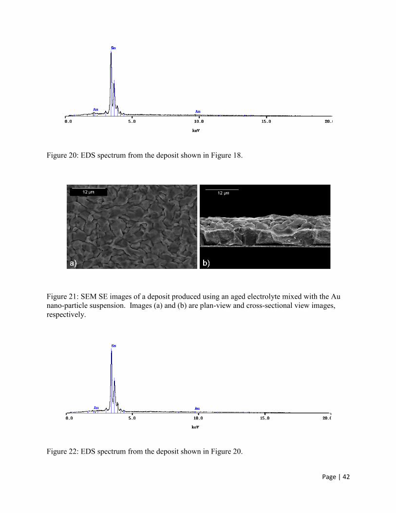
Page | 42
Figure 20: EDS spectrum from the deposit shown in Figure 18.
Figure 21: SEM SE images of a deposit produced using an aged electrolyte mixed with the Au
nano-particle suspension. Images (a) and (b) are plan-view and cross-sectional view images,
respectively.
Figure 22: EDS spectrum from the deposit shown in Figure 20.
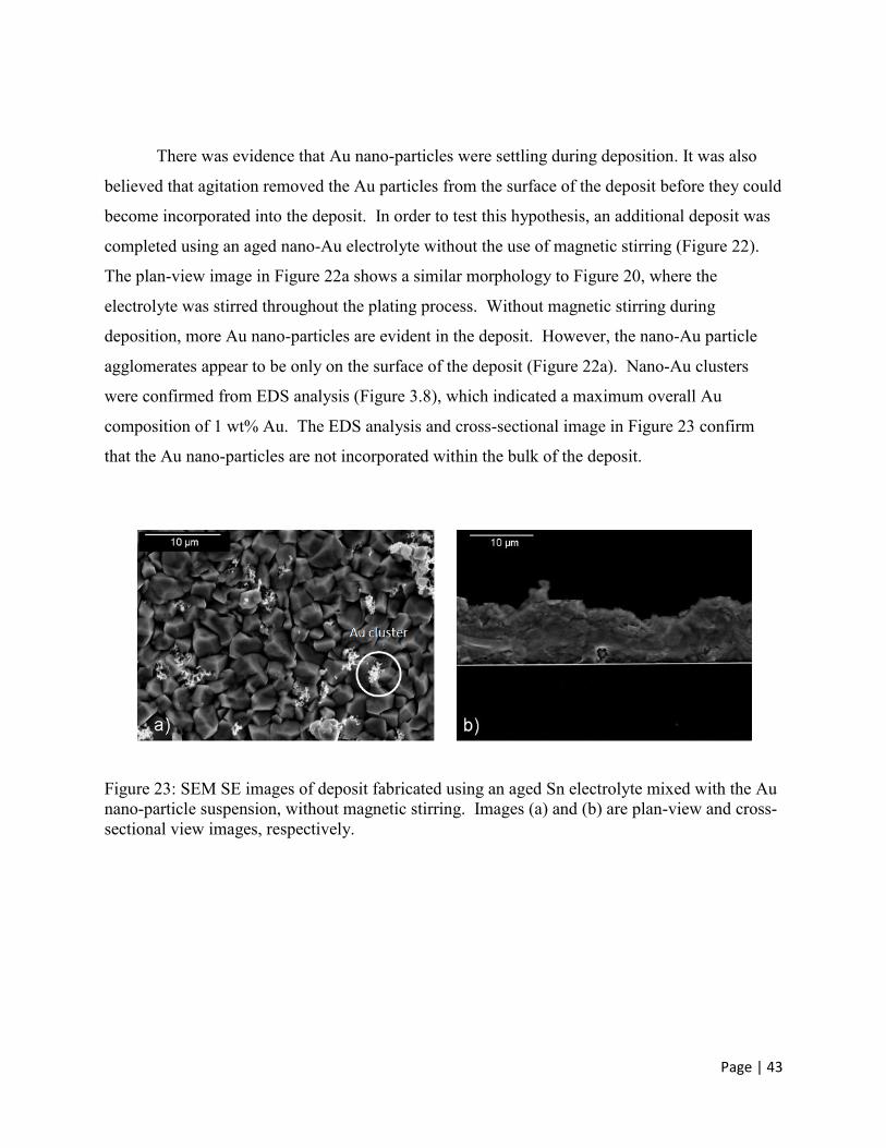
Page | 43
There was evidence that Au nano-particles were settling during deposition. It was also
believed that agitation removed the Au particles from the surface of the deposit before they could
become incorporated into the deposit. In order to test this hypothesis, an additional deposit was
completed using an aged nano-Au electrolyte without the use of magnetic stirring (Figure 22).
The plan-view image in Figure 22a shows a similar morphology to Figure 20, where the
electrolyte was stirred throughout the plating process. Without magnetic stirring during
deposition, more Au nano-particles are evident in the deposit. However, the nano-Au particle
agglomerates appear to be only on the surface of the deposit (Figure 22a). Nano-Au clusters
were confirmed from EDS analysis (Figure 3.8), which indicated a maximum overall Au
composition of 1 wt% Au. The EDS analysis and cross-sectional image in Figure 23 confirm
that the Au nano-particles are not incorporated within the bulk of the deposit.
Figure 23: SEM SE images of deposit fabricated using an aged Sn electrolyte mixed with the Au
nano-particle suspension, without magnetic stirring. Images (a) and (b) are plan-view and cross-
sectional view images, respectively.
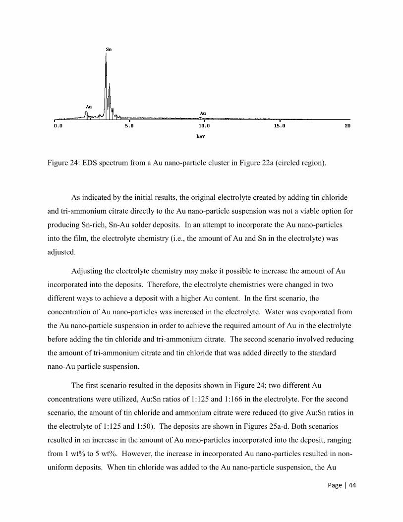
Page | 44
Figure 24: EDS spectrum from a Au nano-particle cluster in Figure 22a (circled region).
As indicated by the initial results, the original electrolyte created by adding tin chloride
and tri-ammonium citrate directly to the Au nano-particle suspension was not a viable option for
producing Sn-rich, Sn-Au solder deposits. In an attempt to incorporate the Au nano-particles
into the film, the electrolyte chemistry (i.e., the amount of Au and Sn in the electrolyte) was
adjusted.
Adjusting the electrolyte chemistry may make it possible to increase the amount of Au
incorporated into the deposits. Therefore, the electrolyte chemistries were changed in two
different ways to achieve a deposit with a higher Au content. In the first scenario, the
concentration of Au nano-particles was increased in the electrolyte. Water was evaporated from
the Au nano-particle suspension in order to achieve the required amount of Au in the electrolyte
before adding the tin chloride and tri-ammonium citrate. The second scenario involved reducing
the amount of tri-ammonium citrate and tin chloride that was added directly to the standard
nano-Au particle suspension.
The first scenario resulted in the deposits shown in Figure 24; two different Au
concentrations were utilized, Au:Sn ratios of 1:125 and 1:166 in the electrolyte. For the second
scenario, the amount of tin chloride and ammonium citrate were reduced (to give Au:Sn ratios in
the electrolyte of 1:125 and 1:50). The deposits are shown in Figures 25a-d. Both scenarios
resulted in an increase in the amount of Au nano-particles incorporated into the deposit, ranging
from 1 wt% to 5 wt%. However, the increase in incorporated Au nano-particles resulted in non-
uniform deposits. When tin chloride was added to the Au nano-particle suspension, the Au
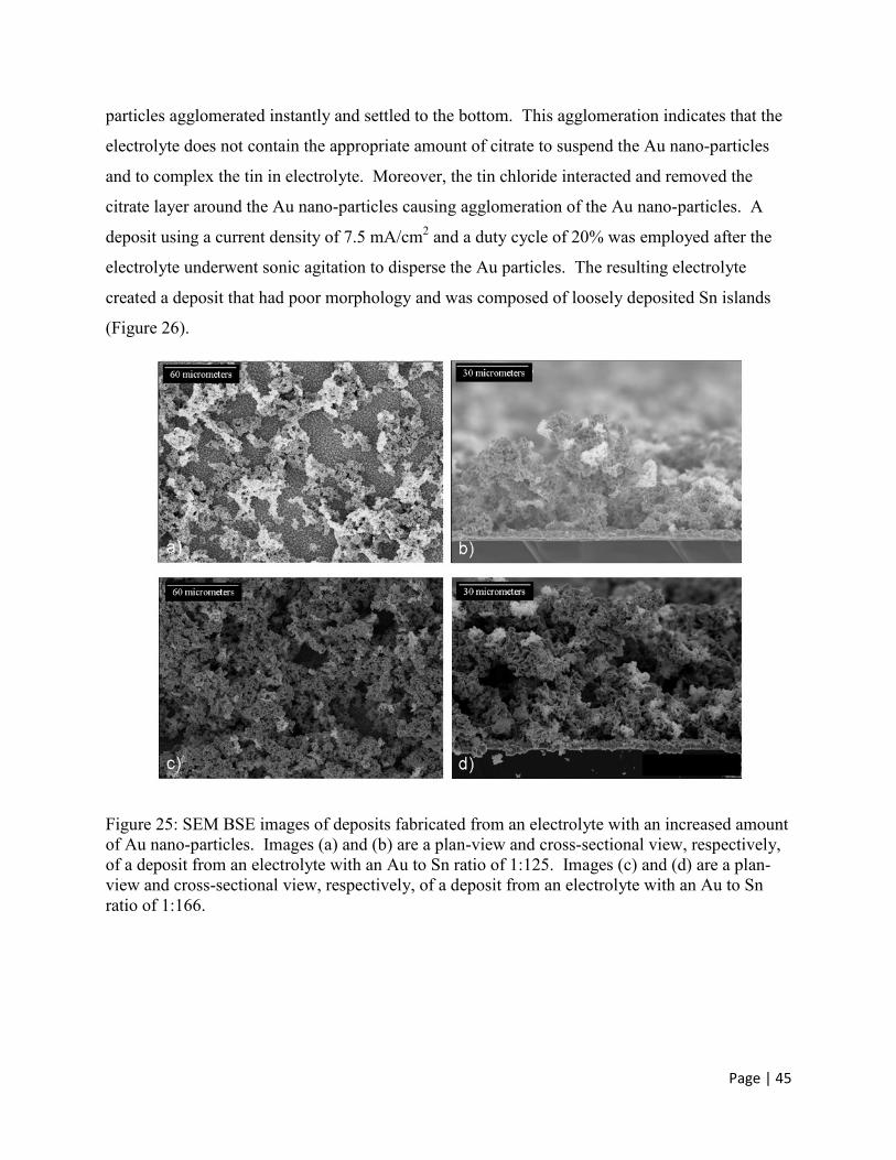
Page | 45
particles agglomerated instantly and settled to the bottom. This agglomeration indicates that the
electrolyte does not contain the appropriate amount of citrate to suspend the Au nano-particles
and to complex the tin in electrolyte. Moreover, the tin chloride interacted and removed the
citrate layer around the Au nano-particles causing agglomeration of the Au nano-particles. A
deposit using a current density of 7.5 mA/cm2 and a duty cycle of 20% was employed after the
electrolyte underwent sonic agitation to disperse the Au particles. The resulting electrolyte
created a deposit that had poor morphology and was composed of loosely deposited Sn islands
(Figure 26).
Figure 25: SEM BSE images of deposits fabricated from an electrolyte with an increased amount
of Au nano-particles. Images (a) and (b) are a plan-view and cross-sectional view, respectively,
of a deposit from an electrolyte with an Au to Sn ratio of 1:125. Images (c) and (d) are a plan-
view and cross-sectional view, respectively, of a deposit from an electrolyte with an Au to Sn
ratio of 1:166.
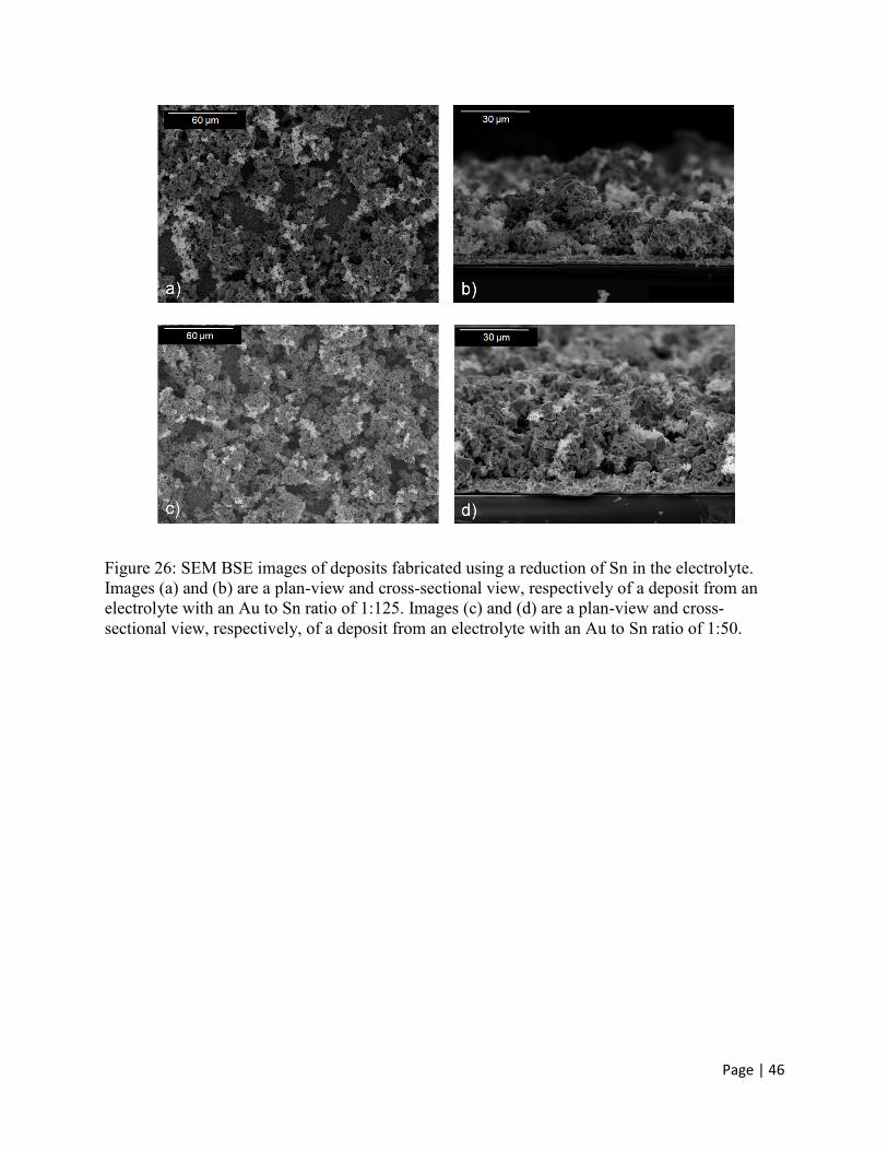
Page | 46
Figure 26: SEM BSE images of deposits fabricated using a reduction of Sn in the electrolyte.
Images (a) and (b) are a plan-view and cross-sectional view, respectively of a deposit from an
electrolyte with an Au to Sn ratio of 1:125. Images (c) and (d) are a plan-view and cross-
sectional view, respectively, of a deposit from an electrolyte with an Au to Sn ratio of 1:50.
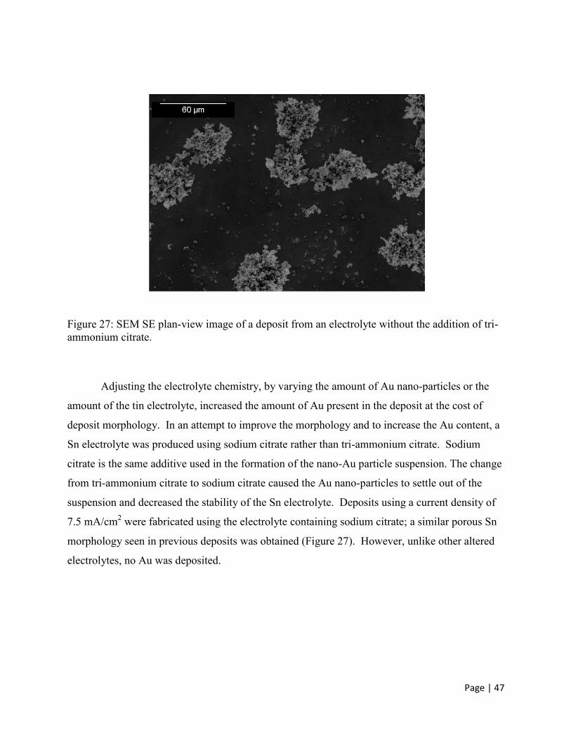
Page | 47
Figure 27: SEM SE plan-view image of a deposit from an electrolyte without the addition of tri-
ammonium citrate.
Adjusting the electrolyte chemistry, by varying the amount of Au nano-particles or the
amount of the tin electrolyte, increased the amount of Au present in the deposit at the cost of
deposit morphology. In an attempt to improve the morphology and to increase the Au content, a
Sn electrolyte was produced using sodium citrate rather than tri-ammonium citrate. Sodium
citrate is the same additive used in the formation of the nano-Au particle suspension. The change
from tri-ammonium citrate to sodium citrate caused the Au nano-particles to settle out of the
suspension and decreased the stability of the Sn electrolyte. Deposits using a current density of
7.5 mA/cm2 were fabricated using the electrolyte containing sodium citrate; a similar porous Sn
morphology seen in previous deposits was obtained (Figure 27). However, unlike other altered
electrolytes, no Au was deposited.
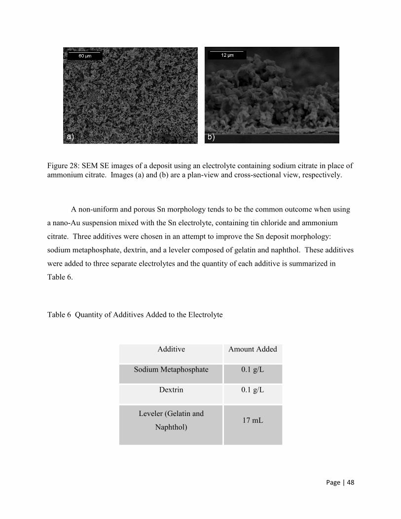
Page | 48
Figure 28: SEM SE images of a deposit using an electrolyte containing sodium citrate in place of
ammonium citrate. Images (a) and (b) are a plan-view and cross-sectional view, respectively.
A non-uniform and porous Sn morphology tends to be the common outcome when using
a nano-Au suspension mixed with the Sn electrolyte, containing tin chloride and ammonium
citrate. Three additives were chosen in an attempt to improve the Sn deposit morphology:
sodium metaphosphate, dextrin, and a leveler composed of gelatin and naphthol. These additives
were added to three separate electrolytes and the quantity of each additive is summarized in
Table 6.
Table 6 Quantity of Additives Added to the Electrolyte
Additive Amount Added
Sodium Metaphosphate 0.1 g/L
Dextrin 0.1 g/L
Leveler (Gelatin and
Naphthol) 17 mL
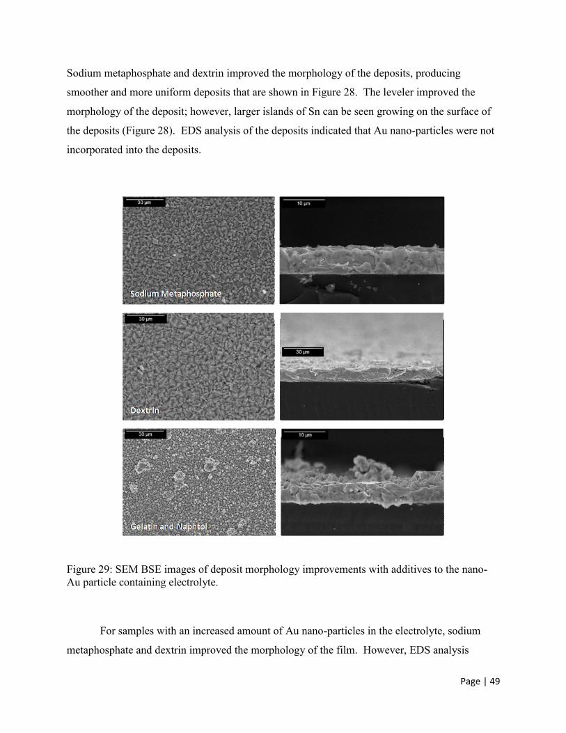
Page | 49
Sodium metaphosphate and dextrin improved the morphology of the deposits, producing
smoother and more uniform deposits that are shown in Figure 28. The leveler improved the
morphology of the deposit; however, larger islands of Sn can be seen growing on the surface of
the deposits (Figure 28). EDS analysis of the deposits indicated that Au nano-particles were not
incorporated into the deposits.
Figure 29: SEM BSE images of deposit morphology improvements with additives to the nano-
Au particle containing electrolyte.
For samples with an increased amount of Au nano-particles in the electrolyte, sodium
metaphosphate and dextrin improved the morphology of the film. However, EDS analysis
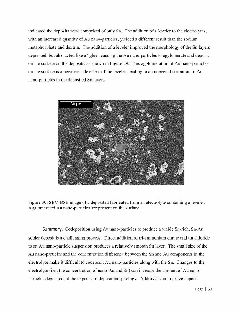
Page | 50
indicated the deposits were comprised of only Sn. The addition of a leveler to the electrolytes,
with an increased quantity of Au nano-particles, yielded a different result than the sodium
metaphosphate and dextrin. The addition of a leveler improved the morphology of the Sn layers
deposited, but also acted like a “glue” causing the Au nano-particles to agglomerate and deposit
on the surface on the deposits, as shown in Figure 29. This agglomeration of Au nano-particles
on the surface is a negative side effect of the leveler, leading to an uneven distribution of Au
nano-particles in the deposited Sn layers.
Figure 30: SEM BSE image of a deposited fabricated from an electrolyte containing a leveler.
Agglomerated Au nano-particles are present on the surface.
Summary. Codeposition using Au nano-particles to produce a viable Sn-rich, Sn-Au
solder deposit is a challenging process. Direct addition of tri-ammonium citrate and tin chloride
to an Au nano-particle suspension produces a relatively smooth Sn layer. The small size of the
Au nano-particles and the concentration difference between the Sn and Au components in the
electrolyte make it difficult to codeposit Au nano-particles along with the Sn. Changes to the
electrolyte (i.e., the concentration of nano-Au and Sn) can increase the amount of Au nano-
particles deposited, at the expense of deposit morphology. Additives can improve deposit

Page | 51
morphology, but inevitably prevent incorporation of Au nano-particles into the deposit. Since
the relationship between Sn deposit morphology and incorporation of Au nano-particles is
complex, a decision was made to develop a different electrolyte. Instead of an Au nano-particle
suspension as the Au source, submicron Au particles were added directly to the Sn electrolyte.
The direct addition of submicron Au particles simplifies the electrochemistry, producing a
simple electrodeposition procedure that enables the goal of producing simple and cost-effective
solder films. This work will be presented in the next chapter.
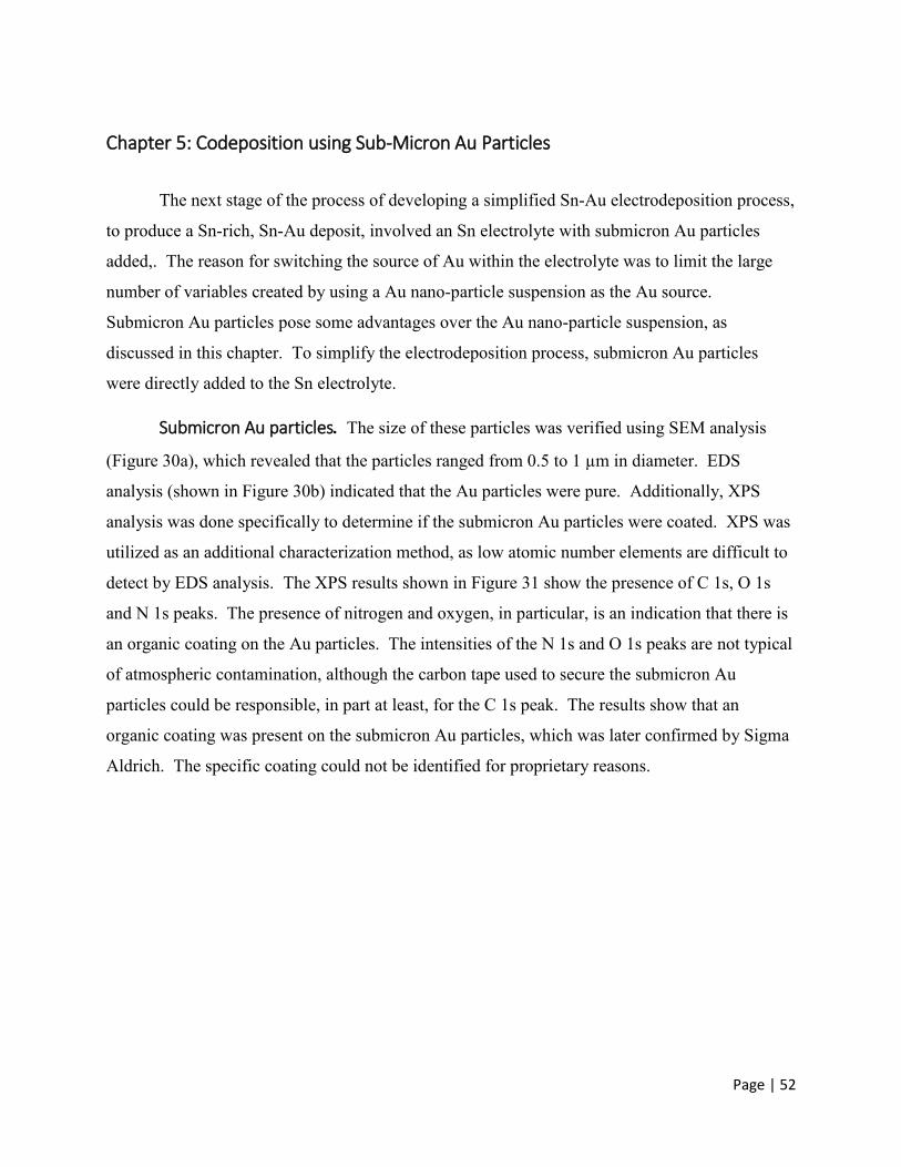
Page | 52
Chapter 5: Codeposition using Sub-Micron Au Particles
The next stage of the process of developing a simplified Sn-Au electrodeposition process,
to produce a Sn-rich, Sn-Au deposit, involved an Sn electrolyte with submicron Au particles
added,. The reason for switching the source of Au within the electrolyte was to limit the large
number of variables created by using a Au nano-particle suspension as the Au source.
Submicron Au particles pose some advantages over the Au nano-particle suspension, as
discussed in this chapter. To simplify the electrodeposition process, submicron Au particles
were directly added to the Sn electrolyte.
Submicron Au particles. The size of these particles was verified using SEM analysis
(Figure 30a), which revealed that the particles ranged from 0.5 to 1 µm in diameter. EDS
analysis (shown in Figure 30b) indicated that the Au particles were pure. Additionally, XPS
analysis was done specifically to determine if the submicron Au particles were coated. XPS was
utilized as an additional characterization method, as low atomic number elements are difficult to
detect by EDS analysis. The XPS results shown in Figure 31 show the presence of C 1s, O 1s
and N 1s peaks. The presence of nitrogen and oxygen, in particular, is an indication that there is
an organic coating on the Au particles. The intensities of the N 1s and O 1s peaks are not typical
of atmospheric contamination, although the carbon tape used to secure the submicron Au
particles could be responsible, in part at least, for the C 1s peak. The results show that an
organic coating was present on the submicron Au particles, which was later confirmed by Sigma
Aldrich. The specific coating could not be identified for proprietary reasons.
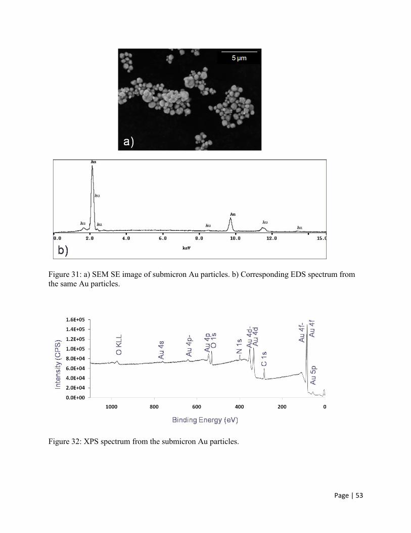
Page | 53
Figure 31: a) SEM SE image of submicron Au particles. b) Corresponding EDS spectrum from
the same Au particles.
Figure 32: XPS spectrum from the submicron Au particles.
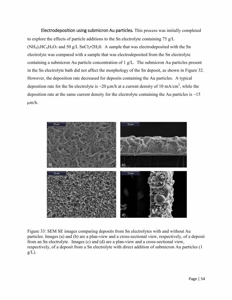
Page | 54
Electrodeposition using submicron Au particles. This process was initially completed
to explore the effects of particle additions to the Sn electrolyte containing 75 g/L
(NH4)3HC6H5O7 and 50 g/L SnCl2•2H20. A sample that was electrodeposited with the Sn
electrolyte was compared with a sample that was electrodeposited from the Sn electrolyte
containing a submicron Au particle concentration of 1 g/L. The submicron Au particles present
in the Sn electrolyte bath did not affect the morphology of the Sn deposit, as shown in Figure 32.
However, the deposition rate decreased for deposits containing the Au particles. A typical
deposition rate for the Sn electrolyte is ~20 m/h at a current density of 10 mA/cm2, while the
deposition rate at the same current density for the electrolyte containing the Au particles is ~15
m/h.
Figure 33: SEM SE images comparing deposits from Sn electrolytes with and without Au
particles. Images (a) and (b) are a plan-view and a cross-sectional view, respectively, of a deposit
from an Sn electrolyte. Images (c) and (d) are a plan-view and a cross-sectional view,
respectively, of a deposit from a Sn electrolyte with direct addition of submicron Au particles (1
g/L).
Page | 55
The next approach was to determine effect of current density on the morphology and
composition of the solder film. Pulse current and direct current were used to determine the
effects of current density. To ensure that current density was the only factor being explored, the
experimental setup was fixed and a fresh electrolyte was used for each experiment. Fresh
electrolytes were used to eliminate any changes in deposit composition that may arise from
consumption of submicron Au particles during the deposition process. The Au particle loading
was fixed at 1 g/L. The results of adjusting current density are shown in Figure 33. The organic
coating did not affect the deposition of submicron Au particles when the current density was
changed. As the current density was increased from 5 to 15 mA/cm2, the deposit composition
remained constant at around 5–6 wt%, as shown in Figure 33. Moreover, the deposit
morphology over the range of 5–10 mA/cm2 remained smooth.
Direct current deposition, shown in Figure 34, was also used to investigate the effect on
the composition of the deposit. The continual buildup of the Sn layer or increase in surface
roughness may incorporate more Au particles by trapping them during deposition. However,
EDS analysis of the samples indicates the composition ranged from 4.5–6 wt% Au, which is
similar to the deposits created using pulse deposition. Thus, the incorporation of Au particles
into the deposit is not influenced by the deposition process or current density used.
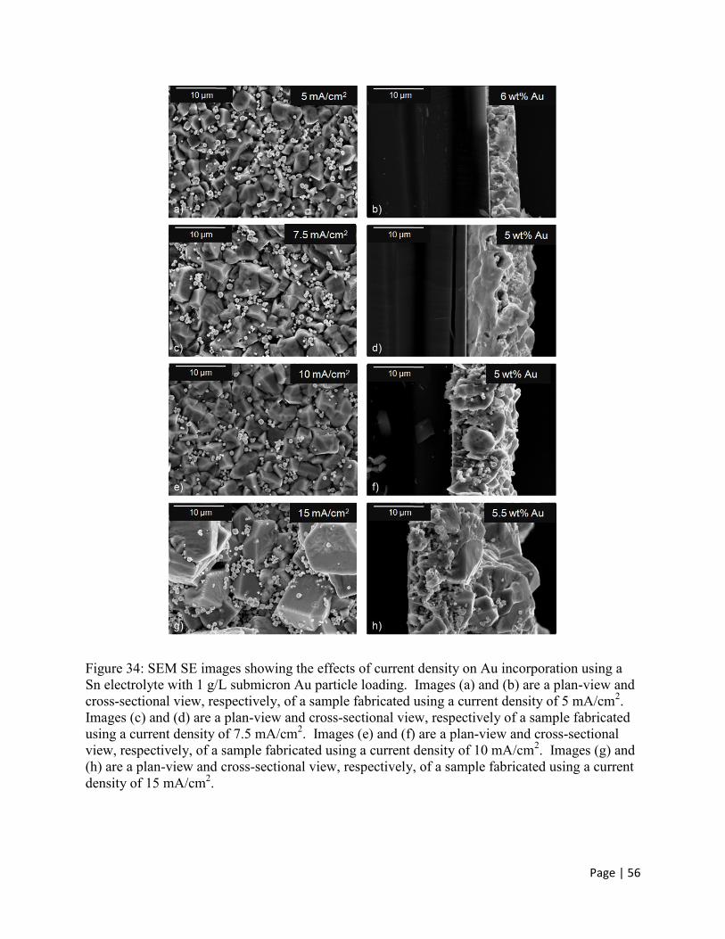
Page | 56
Figure 34: SEM SE images showing the effects of current density on Au incorporation using a
Sn electrolyte with 1 g/L submicron Au particle loading. Images (a) and (b) are a plan-view and
cross-sectional view, respectively, of a sample fabricated using a current density of 5 mA/cm2.
Images (c) and (d) are a plan-view and cross-sectional view, respectively of a sample fabricated
using a current density of 7.5 mA/cm2. Images (e) and (f) are a plan-view and cross-sectional
view, respectively, of a sample fabricated using a current density of 10 mA/cm2. Images (g) and
(h) are a plan-view and cross-sectional view, respectively, of a sample fabricated using a current
density of 15 mA/cm2.
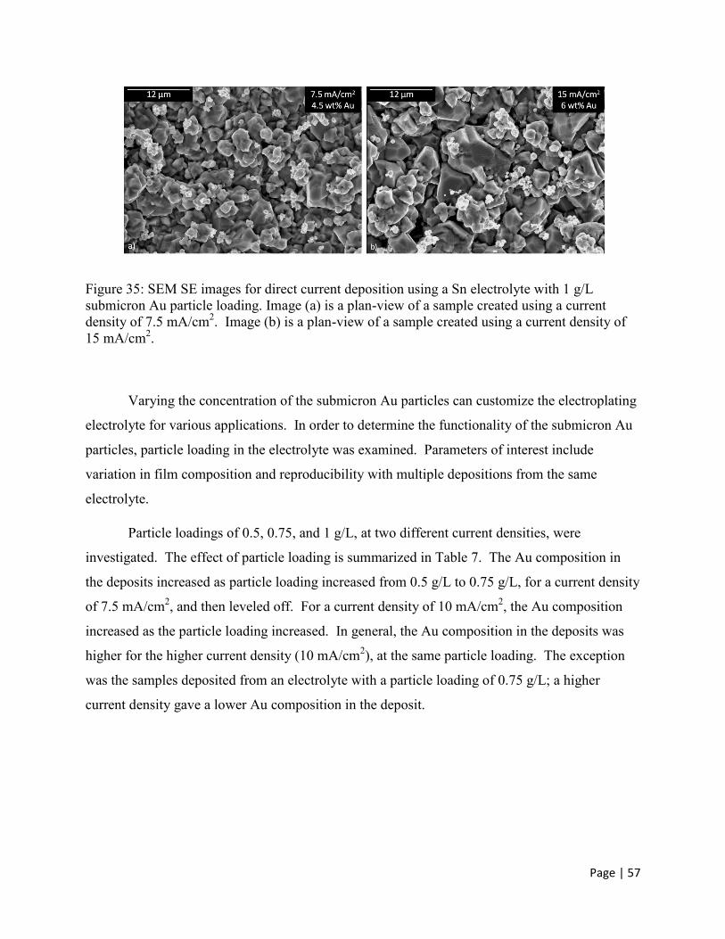
Page | 57
Figure 35: SEM SE images for direct current deposition using a Sn electrolyte with 1 g/L
submicron Au particle loading. Image (a) is a plan-view of a sample created using a current
density of 7.5 mA/cm2. Image (b) is a plan-view of a sample created using a current density of
15 mA/cm2.
Varying the concentration of the submicron Au particles can customize the electroplating
electrolyte for various applications. In order to determine the functionality of the submicron Au
particles, particle loading in the electrolyte was examined. Parameters of interest include
variation in film composition and reproducibility with multiple depositions from the same
electrolyte.
Particle loadings of 0.5, 0.75, and 1 g/L, at two different current densities, were
investigated. The effect of particle loading is summarized in Table 7. The Au composition in
the deposits increased as particle loading increased from 0.5 g/L to 0.75 g/L, for a current density
of 7.5 mA/cm2, and then leveled off. For a current density of 10 mA/cm
2, the Au composition
increased as the particle loading increased. In general, the Au composition in the deposits was
higher for the higher current density (10 mA/cm2), at the same particle loading. The exception
was the samples deposited from an electrolyte with a particle loading of 0.75 g/L; a higher
current density gave a lower Au composition in the deposit.
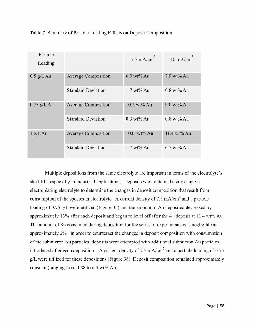
Page | 58
Table 7 Summary of Particle Loading Effects on Deposit Composition
Particle
Loading 7.5 mA/cm
2 10 mA/cm
2
0.5 g/L Au Average Composition 6.0 wt% Au 7.9 wt% Au
Standard Deviation 1.7 wt% Au 0.8 wt% Au
0.75 g/L Au Average Composition 10.2 wt% Au 9.0 wt% Au
Standard Deviation 0.3 wt% Au 0.8 wt% Au
1 g/L Au Average Composition 10.0 wt% Au 11.4 wt% Au
Standard Deviation 1.7 wt% Au 0.5 wt% Au
Multiple depositions from the same electrolyte are important in terms of the electrolyte’s
shelf life, especially in industrial applications. Deposits were obtained using a single
electroplating electrolyte to determine the changes in deposit composition that result from
consumption of the species in electrolyte. A current density of 7.5 mA/cm2 and a particle
loading of 0.75 g/L were utilized (Figure 35) and the amount of Au deposited decreased by
approximately 13% after each deposit and began to level off after the 4th
deposit at 11.4 wt% Au.
The amount of Sn consumed during deposition for the series of experiments was negligible at
approximately 2%. In order to counteract the changes in deposit composition with consumption
of the submicron Au particles, deposits were attempted with additional submicron Au particles
introduced after each deposition. A current density of 7.5 mA/cm2 and a particle loading of 0.75
g/L were utilized for these depositions (Figure 36). Deposit composition remained approximately
constant (ranging from 4.88 to 6.5 wt% Au).
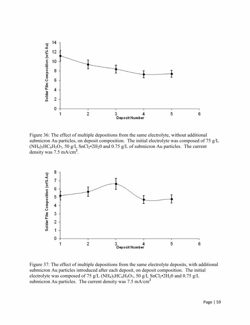
Page | 59
Figure 36: The effect of multiple depositions from the same electrolyte, without additional
submicron Au particles, on deposit composition. The initial electrolyte was composed of 75 g/L
(NH4)3HC6H5O7, 50 g/L SnCl2•2H20 and 0.75 g/L of submicron Au particles. The current
density was 7.5 mA/cm2.
Figure 37: The effect of multiple depositions from the same electrolyte deposits, with additional
submicron Au particles introduced after each deposit, on deposit composition. The initial
electrolyte was composed of 75 g/L (NH4)3HC6H5O7, 50 g/L SnCl2•2H20 and 0.75 g/L
submicron Au particles. The current density was 7.5 mA/cm2
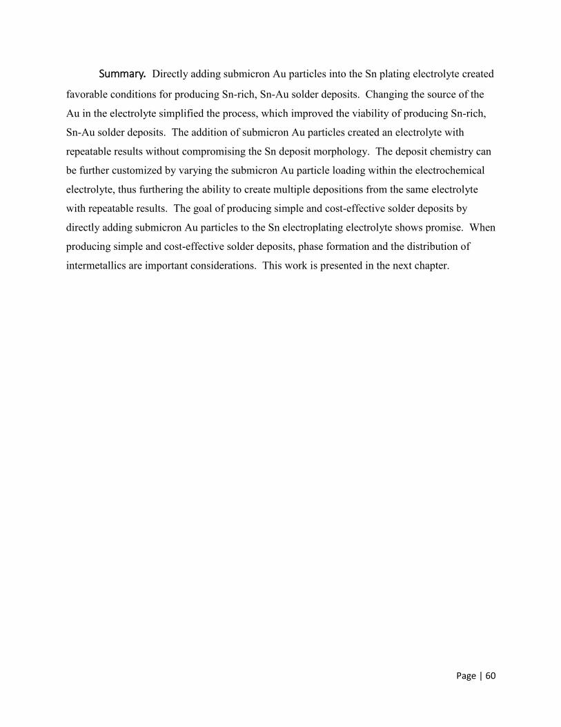
Page | 60
Summary. Directly adding submicron Au particles into the Sn plating electrolyte created
favorable conditions for producing Sn-rich, Sn-Au solder deposits. Changing the source of the
Au in the electrolyte simplified the process, which improved the viability of producing Sn-rich,
Sn-Au solder deposits. The addition of submicron Au particles created an electrolyte with
repeatable results without compromising the Sn deposit morphology. The deposit chemistry can
be further customized by varying the submicron Au particle loading within the electrochemical
electrolyte, thus furthering the ability to create multiple depositions from the same electrolyte
with repeatable results. The goal of producing simple and cost-effective solder deposits by
directly adding submicron Au particles to the Sn electroplating electrolyte shows promise. When
producing simple and cost-effective solder deposits, phase formation and the distribution of
intermetallics are important considerations. This work is presented in the next chapter.
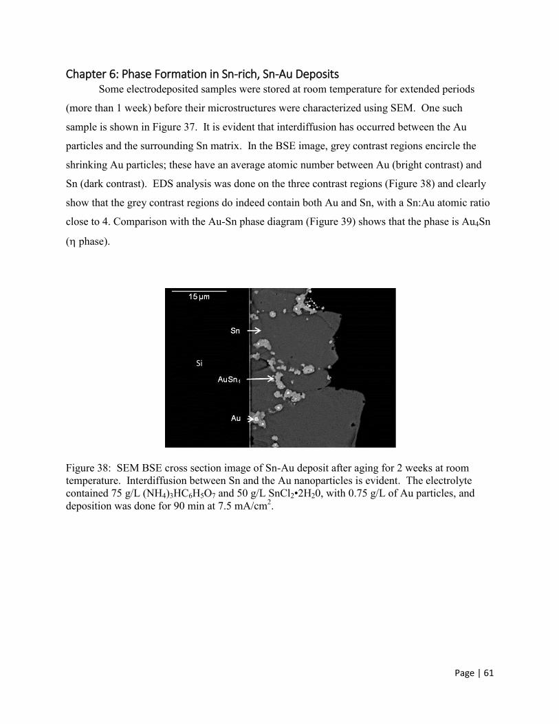
Page | 61
Chapter 6: Phase Formation in Sn-rich, Sn-Au Deposits Some electrodeposited samples were stored at room temperature for extended periods
(more than 1 week) before their microstructures were characterized using SEM. One such
sample is shown in Figure 37. It is evident that interdiffusion has occurred between the Au
particles and the surrounding Sn matrix. In the BSE image, grey contrast regions encircle the
shrinking Au particles; these have an average atomic number between Au (bright contrast) and
Sn (dark contrast). EDS analysis was done on the three contrast regions (Figure 38) and clearly
show that the grey contrast regions do indeed contain both Au and Sn, with a Sn:Au atomic ratio
close to 4. Comparison with the Au-Sn phase diagram (Figure 39) shows that the phase is Au4Sn
( phase).
Figure 38: SEM BSE cross section image of Sn-Au deposit after aging for 2 weeks at room
temperature. Interdiffusion between Sn and the Au nanoparticles is evident. The electrolyte
contained 75 g/L (NH4)3HC6H5O7 and 50 g/L SnCl2•2H20, with 0.75 g/L of Au particles, and
deposition was done for 90 min at 7.5 mA/cm2.
Si
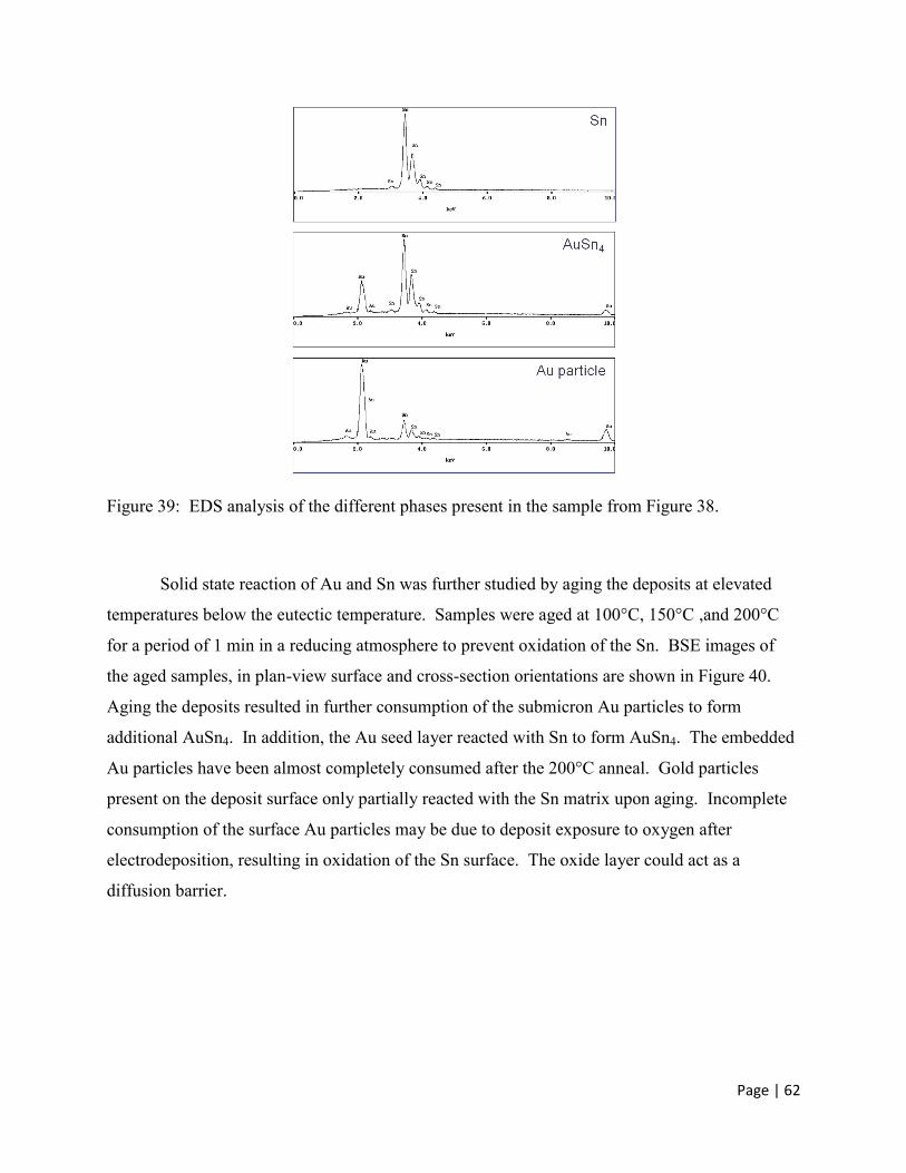
Page | 62
Figure 39: EDS analysis of the different phases present in the sample from Figure 38.
Solid state reaction of Au and Sn was further studied by aging the deposits at elevated
temperatures below the eutectic temperature. Samples were aged at 100°C, 150°C ,and 200°C
for a period of 1 min in a reducing atmosphere to prevent oxidation of the Sn. BSE images of
the aged samples, in plan-view surface and cross-section orientations are shown in Figure 40.
Aging the deposits resulted in further consumption of the submicron Au particles to form
additional AuSn4. In addition, the Au seed layer reacted with Sn to form AuSn4. The embedded
Au particles have been almost completely consumed after the 200°C anneal. Gold particles
present on the deposit surface only partially reacted with the Sn matrix upon aging. Incomplete
consumption of the surface Au particles may be due to deposit exposure to oxygen after
electrodeposition, resulting in oxidation of the Sn surface. The oxide layer could act as a
diffusion barrier.
Page | 63
Figure 40: SEM BSE images (cross-section and plan-view) of Sn-Au deposits after aging at
elevated temperatures below the eutectic temperature. The deposit in images (a) and (b) was
exposed to 100°C for 1 min. The deposit in images (c) and (d) was exposed to 150°C for 1 min.
The deposit in images (e) and (f) was exposed to 200°C for 1 min.
Additional samples were investigated at temperatures above the eutectic temperature
(~232°C). Reflow was used to ensure complete reaction between the submicron Au particles and
Sn matrix, and was done in a reducing atmosphere at temperatures of 250°C, 260°C, and 270°C
(Figure 40). Analysis of the reflowed samples revealed similar interactions between the
submicron Au particles and the Sn matrix as well as between the Au seed layer and the Sn
matrix. Incomplete reaction between the surface Au particles and the Sn matrix is still evident
even at elevated reflow temperatures.
Si
Si
Si
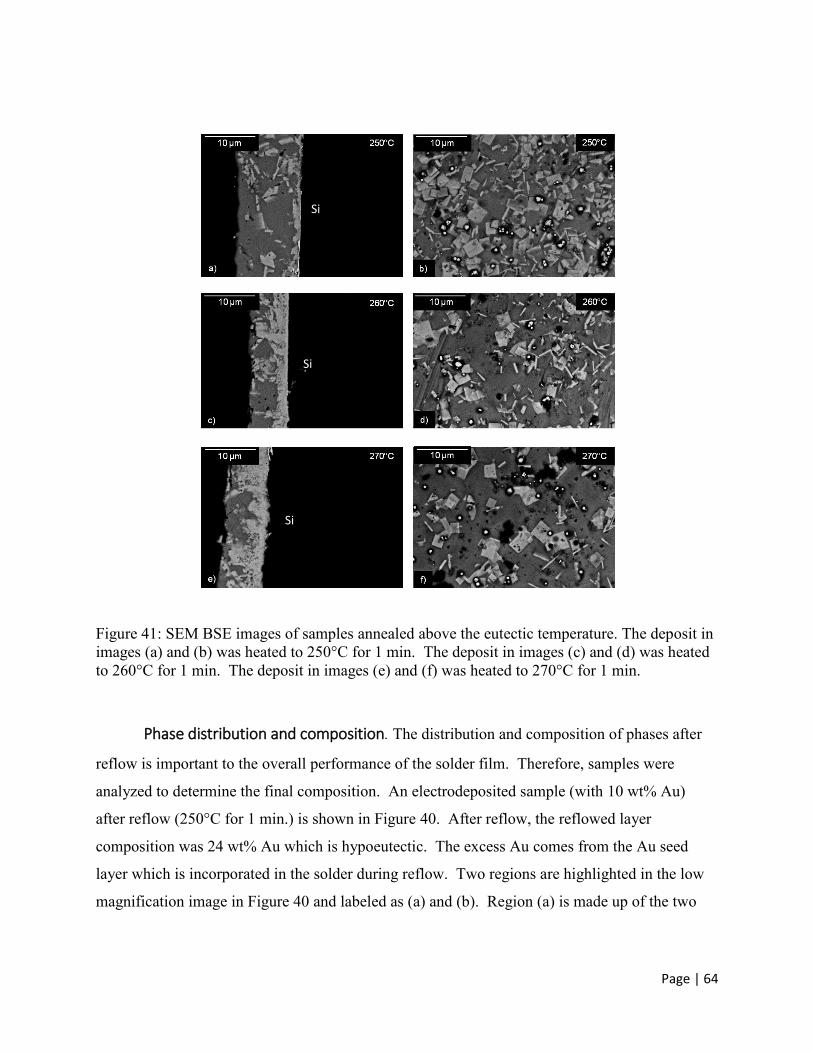
Page | 64
Figure 41: SEM BSE images of samples annealed above the eutectic temperature. The deposit in
images (a) and (b) was heated to 250°C for 1 min. The deposit in images (c) and (d) was heated
to 260°C for 1 min. The deposit in images (e) and (f) was heated to 270°C for 1 min.
Phase distribution and composition. The distribution and composition of phases after
reflow is important to the overall performance of the solder film. Therefore, samples were
analyzed to determine the final composition. An electrodeposited sample (with 10 wt% Au)
after reflow (250°C for 1 min.) is shown in Figure 40. After reflow, the reflowed layer
composition was 24 wt% Au which is hypoeutectic. The excess Au comes from the Au seed
layer which is incorporated in the solder during reflow. Two regions are highlighted in the low
magnification image in Figure 40 and labeled as (a) and (b). Region (a) is made up of the two
Si
Si
Si
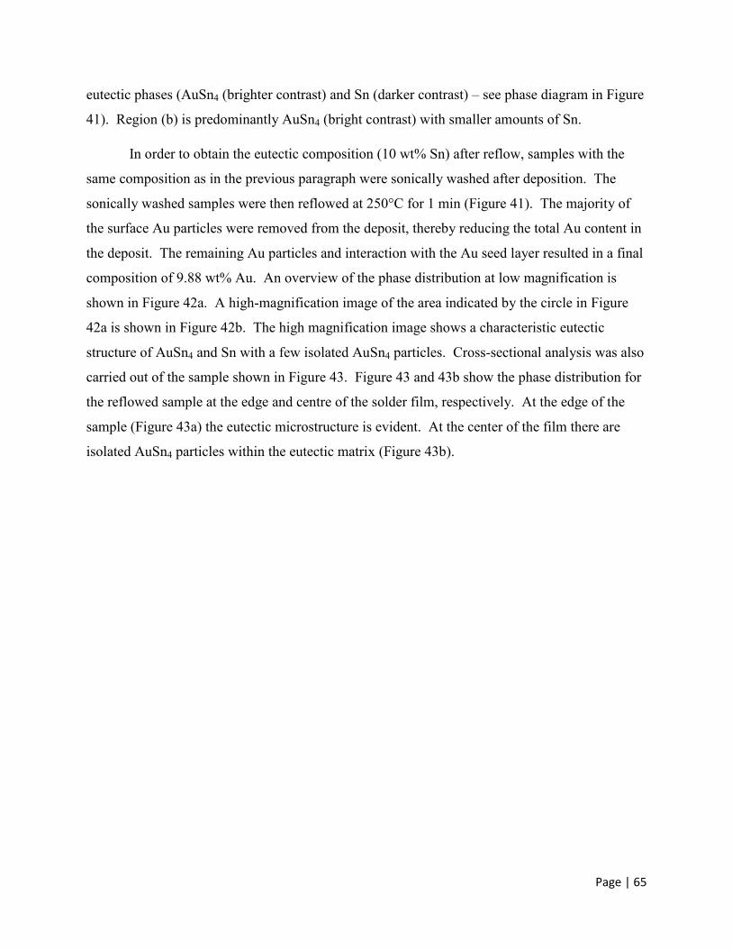
Page | 65
eutectic phases (AuSn4 (brighter contrast) and Sn (darker contrast) – see phase diagram in Figure
41). Region (b) is predominantly AuSn4 (bright contrast) with smaller amounts of Sn.
In order to obtain the eutectic composition (10 wt% Sn) after reflow, samples with the
same composition as in the previous paragraph were sonically washed after deposition. The
sonically washed samples were then reflowed at 250°C for 1 min (Figure 41). The majority of
the surface Au particles were removed from the deposit, thereby reducing the total Au content in
the deposit. The remaining Au particles and interaction with the Au seed layer resulted in a final
composition of 9.88 wt% Au. An overview of the phase distribution at low magnification is
shown in Figure 42a. A high-magnification image of the area indicated by the circle in Figure
42a is shown in Figure 42b. The high magnification image shows a characteristic eutectic
structure of AuSn4 and Sn with a few isolated AuSn4 particles. Cross-sectional analysis was also
carried out of the sample shown in Figure 43. Figure 43 and 43b show the phase distribution for
the reflowed sample at the edge and centre of the solder film, respectively. At the edge of the
sample (Figure 43a) the eutectic microstructure is evident. At the center of the film there are
isolated AuSn4 particles within the eutectic matrix (Figure 43b).
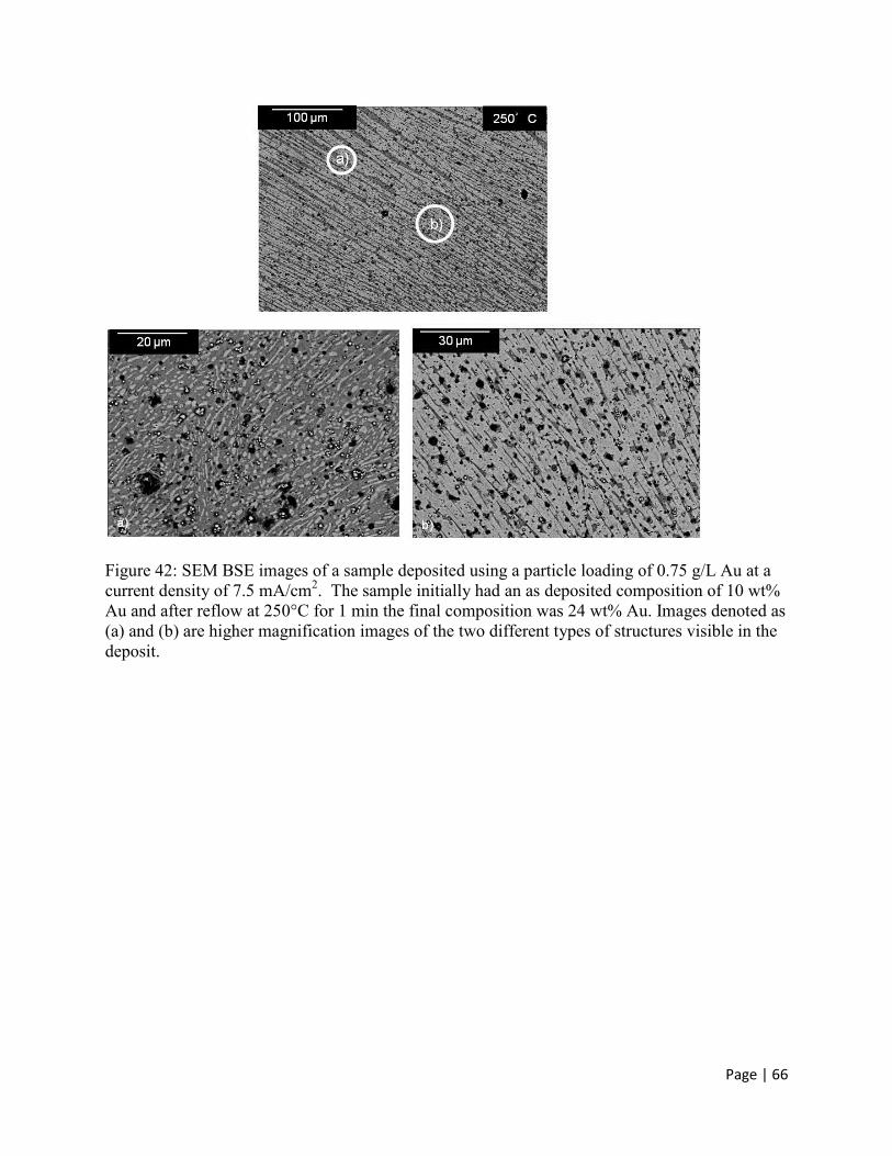
Page | 66
Figure 42: SEM BSE images of a sample deposited using a particle loading of 0.75 g/L Au at a
current density of 7.5 mA/cm2. The sample initially had an as deposited composition of 10 wt%
Au and after reflow at 250°C for 1 min the final composition was 24 wt% Au. Images denoted as
(a) and (b) are higher magnification images of the two different types of structures visible in the
deposit.
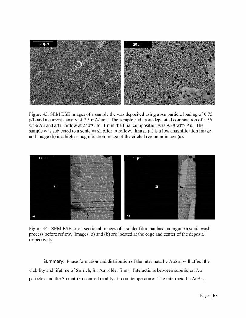
Page | 67
Figure 43: SEM BSE images of a sample the was deposited using a Au particle loading of 0.75
g/L and a current density of 7.5 mA/cm2. The sample had an as deposited composition of 4.56
wt% Au and after reflow at 250°C for 1 min the final composition was 9.88 wt% Au. The
sample was subjected to a sonic wash prior to reflow. Image (a) is a low-magnification image
and image (b) is a higher magnification image of the circled region in image (a).
Figure 44: SEM BSE cross-sectional images of a solder film that has undergone a sonic wash
process before reflow. Images (a) and (b) are located at the edge and center of the deposit,
respectively.
Summary. Phase formation and distribution of the intermetallic AuSn4 will affect the
viability and lifetime of Sn-rich, Sn-Au solder films. Interactions between submicron Au
particles and the Sn matrix occurred readily at room temperature. The intermetallic AuSn4
Si Si
Page | 68
formed around the deposited Au particles, which were located along the grain boundaries of the
electrodeposited Sn. Gold particles deposited on the surface did not react with the Sn matrix.
Aging the deposits at elevated temperatures below the eutectic temperature increased the amount
of interaction between the submicron Au particles and the Sn matrix, further driving the reaction
and increasing the amount of intermetallic AuSn4 formed in the deposit. Additionally, aging the
deposits caused the intermetallic AuSn4 to form at the interface between the Au seed layer and
the Sn matrix. Reflow of the Sn-rich, Sn-Au solder deposit was carried out to ensure complete
interaction of the submicron Au particles and the Sn matrix. Complete interaction of deposited
eutectic Sn-rich, Sn-Au films with the Au seed layer produced a hypoeutectic composition with a
high concentration of intermetallic AuSn4. Sonic cleaning of composition deposits reduced the
as-deposited composition to 9.88 wt% Au. Reflow of sonically cleaned deposits generated a
eutectic composition and microstructure after reflow. The goal of producing simple and cost-
effective eutectic solder films using direct addition of submicron Au particles to a simple Sn
electrolyte shows promise.
Page | 69
Chapter 7: Conclusions and Future Work
Final Conclusions The Sn-rich eutectic alloy (90 wt% Sn) in the Au-Sn system offers a potentially cheaper
alternative to the Au-rich eutectic alloy (20 wt% Sn) for optoelectronic and
microelectromechanical systems (MEMS) device packaging and may be applicable as a Pb-free
solder for microelectronic packaging. A life cycle analysis of Au-Sn electrodeposition
development in industry and the scientific background of electrodeposition was provided.
Specific details were given regarding the history of solders, trends in the field, and initiatives to
further develop solders. Considerations regarding design, toxicity and public health impact,
availability of raw materials, and environmental impacts when making decisions in selecting
alternative materials were discussed.
A simple electrodeposition method was utilized to fabricate Sn-rich, Au–Sn solder films,
including the eutectic composition. The electrolyte consisted of a electrolyte of Sn chloride and
ammonium citrate. Gold was added to the electrolyte in the form of either a Au nanoparticle
(<20 nm) suspension, prepared with Na citrate, or by directly adding Au powder (500–800 nm
particles). Historically, electrodeposition has proven to be an economical and valid technology
for producing deposits that may be categorized depending on their main function; i.e., to improve
the appearance of a part, impart a protective surface on a part, or modify the chemical or physical
properties of a part’s surface.
Initially, the co-deposition of Au nano-particles mixed with a Sn plating electrolyte was
explored to produce a viable Sn-rich, Sn-Au solder deposit. Direct addition of tri-ammonium
citrate and Sn chloride to the Au nano-particle suspension produced a relatively smooth Sn layer.
Changes to the electrochemistry of the electrolyte (i.e., the concentration of the nano-Au
suspension and the Sn solution) caused an increase in the amount of the Au nano-particles
deposited at the expense of the film’s morphology. Additives improved the deposit morphology
but inevitably prevented incorporation of the Au nano-particles into the deposit. Since the
relationship between the Sn morphology and incorporation of the Au nano-particles was
complex, a decision was made to develop a different electroplating bath.
Page | 70
In the second approach, the direct addition of Au submicron particles into an Sn plating
electrolyte created favourable conditions for producing Sn-rich, Sn-Au solder deposits.
Changing the source of the Au in the electrolyte simplified the electrochemistry, which improved
the viability of producing Sn-rich, Sn-Au solder deposits. The addition of submicron Au
particles created an electrolyte with repeatable results without compromising the Sn morphology.
Phase formation and distribution of the intermetallic AuSn4 will affect the viability and
lifetime of Sn-rich, Sn-Au solder films. Interactions between submicron Au particles and the Sn
matrix occurred readily at room temperature. Initial intermetallic AuSn4 formed around the
deposited submicron Au particles along the grain boundaries of deposited Sn, while submicron
Au particles deposited on the surface did not react with the Sn matrix. Aging the deposits at
elevated temperatures below the eutectic temperature increased the amount of interaction
between the submicron Au particles and the Sn matrix, further driving the reaction and
increasing the amount of intermetallic AuSn4 formed in the deposit.
Reflow of the Sn-rich, Sn-Au solder deposit was carried out between 250°C and 270°C.
During the reflow process complete interaction of deposited eutectic Sn-rich, Sn-Au films with
the Au seed layer occurred. Reflow of the as deposited samples produced a hypoeutectic
composition with an excess of intermetallic AuSn4. Samples that were sonically cleaned before
reflow had the composition of 9.88 wt% Au.
The Sn-rich, Sn-Au solder composition is not currently used in industry. Thus, there is
an opportunity to explore an alternative composition for solder joints for optoelectronic and
MEMS applications.
Future Work
A more defined statistical analysis and probabilistic assessment could be completed to
further define the viability of Au submicron particle additions into a Sn electrolyte. By
determining the most effective factors influencing the deposit composition and plating rate a
statistical analysis could be complete alongside the deterministic assessment. The resulting
assessment could be used to develop a predictable and consistent method to deposit Sn-rich, Au-
Sn deposits.

Page | 71
The next focal point in studying Sn-rich, Sn-Au solder films could be determining the
capability of creating a bond and the resulting strength of the bond. Phase formation and
distribution of the bonded substrates could be studied by performing pull or shear tests to
determine the bond strength of the reflowed Sn-rich, Au-Sn deposits.
Page | 72
References
American Society for Metals, Binary Alloy Phase Diagrams, Alloy Phase Diagrams Vol 3, ASM
Handbook, ASM International, 2012.
Allebby, B., Artaki, I., Carroll, T., Dahringer, D.W., Degani, Y., Fisher, J.R., Freund, R.S.,
Gherman, C., Graedel, T.E., Lyons, A.M., Melton, C., Munie, G.C., Schoenthaler, D., Plewes,
J.T., Socolowshi, N., Solomon, H. An Assessment of the Use of Lead in Electronic Assembly.
National Surface Mount Council, IPC, 1992.
Bard, A.J., Faulkner, L.R., Electrochemical Methods: Fundamentals and Applications. John
Wiley & Sons, Inc., 2001.
Barkey, D.P; Wu, Q; Keigler, A.; Liu, Z.; Electrocodeposition of Silver Particles with Tin for
Fabrication of Lead-Free Solder Bumps. ECS Transactions, 1, 13, 43-51, 2006.
Boustedt, K., GHz Flip-Chip: An Overview, Electronic Component and Technology Conference,
297-302, 1998.
Chaung, R.W., Lee, C.C., A Fluxless Au-Sn Bonding Process of Tin-Rich Compositions
Achieved in Ambient Air, 52nd
Electronic Components and Technology Conference, 134-137,
2002.
Doesburg, J., Ivey, D.G., Microstructure and Preferred Orientation of Au-Sn Alloy Plated
Deposts, Materials Science and Engineering B, in press, 21 manuscript pages, 2000.
Djurfors, B., Ivey, D.G., Microstructural Characterization of Pulsed Electrodeposited An/Sn
Alloy Thin Films, Materials Science & Engineering B, B90, 3, 309-320, 2002.
Foulke, D.G., Metal Finishing, 67, 4, 50, 1969.
Foulke, D.G., in: Reid, F.H., Goldie, W., Gold PlatingTechnology Chapter 7, Electrochemical
Publications, 52, 1974.
Page | 73
Gamalski, J., A European Perspective from a Global OEM, IPC/Jedec Conference on Lead Free
Electronic Components and Assemeblies, 2002.
Goldstein J.L., Scanning Electron Microsopy and X-ray Microanalysis, Springer Science &
Business Media, LLC, 2003.
He, A., Ivey D.G., Electrodeposition of Tin: A Simple Approach, Journal of Materials Science:
Materials in Electronics, 19, 6, 553-562, 2008.
He, A., Ivey, D.G., Electrodeposition of Sn and Au-Sn alloys from a Single Non-Cyanide
Electrolyte. Journal of Electronic Materials, 23, 12, 2186-2193, 2012.
Jeong, G.H., Kim, J.H., Lee, D., Suh, S.J., Microstructure and Composition of Au-Sn Eutectic
Solder Electroplated from a Single Solution, Materials Research Society Symposium
Proceedings, 894, LL03-16.l-LL03-16.5, 2006.
Kallmayer, C., Lin, D., Kloeser, J., Oppermann, H., Zakel, E., Reichl, H., Fluxless Flip-Chip
Attachment Techniques using Au/Sn Metallurgy. IEEE:CPMT International Electronics
Manufacturing Technology Symposium, 20, 1995.
Kallmayer, C., Lin, D., Oppermann, H., Kloeser, J., Weib, S., Zakel, E., Reichl, H., Fluxless
Flip-Chip Soldering using Eutectic Gold-Tin System: A Comparison between self-alignment and
thermode-bonding, Proceedings of the 10th European Microelectronics Conference, 440, 1995.
Kim, J., Lee, C.C., Fluxless Sn-Rich Sn-Au Flip-Chip Bonding Using Electroplating Process.
10th International Symposium on Advanced Packaging Materials: Processes, Properties and
Interfaces, 164 (2005).
Kim, J., Kim, D., Lee, C.C., Fluxless Flip-Chip Solder Joint Fabrication Using Electroplated Sn-
Rich Sn-Au Structures. IEEE Transactions on Advanced Packaging, 29, 473, 2006.
Kim, J., Lee C.C., Fluxless Wafer Bonding with Sn-rich Sn-Au Dual-Layer Structure, Materials
Science and Engineering, A, 417, 143-148. 2006.
Page | 74
Kim, J.S., Wang, P.J., Lee, C.C., Fluxless Hermetic Lid Sealing Using Electroplated Sn-Rich
Solder, IEEE Transactions on Components and Packaging Technologies, 31, 3, 2008.
Kubota, N., Horikoshi, T., Sato, E., Electrodeposition of Gold-Tin Alloys from Pyrophosphate
Solution, Journal of Metal Finishing Society of Japan, 34, 37-43, 1983.
Ku, A., Lead-Free Solders: Issues of Toxicity, Availability and Impacts of Extraction, 53rd
Electronic Components and Technology Conference Proceedings, 47-53, 2003.
Le Fevre, P.J.F., Environmental Issues in Power Electronics, IEEE Applied Power Electronics
Conference and Exposition, 1, 121-125, 2002.
Lee, C.C., Chuang, R.W., Fluxless Non-Eutectic Joints Fabricated Using Gold-Tin Multilayer
Composite, IEEE Transactions Components and Packaging Technologies, .26, n2, 416-422,
2003.
Lowenhein, F.A., Modern Electroplating, 3rd
Edition. Wiley-Interscience. 1974.
McFarland, A.D., Haynes, C.L., Mirkin, C.A., Van Duyne, R.P., Godwin, H.A., Color My
Nanoworld. Journal of Chemical Education, 81, 4, 544A, 2004.
Morawej, N., Ivey, D.G., A statistical design of experiments (DOE) approach to improving the
process for electrodeposition of gold-tin alloys from chloride-based solution, Journal of Applied
Surface Finishing, 2, 3, 220-225, 2007.
Nimmo, K., Review of European Legislation and Lead Free Technology Roadmap, IPC/Jedec
Conference on Lead Free Electronic Components and Assemblies, 2002.
Paunovic, M., Schlesinger, M., Fundamentals of Electrochemical Deposition 2nd
Edition. John
Wiley & Sons, Inc., 1998.
Paunovic, M., Schlesinger, M., Modern Electroplating, 4th
Edition. The Electrochemical Society,
Inc., 2000.
Raub, C.J., Knodler, A.,Lendvay, L., Plating, 63, 35, 1976.
Page | 75
Reid, F.H., Goldie, W., Gold Plating Technology. Electrochemical Publications, 1974.
Sun, W., Ivey, D.G., Development of an electroplating solution for Codepositing Au–Sn Alloys,
Materials Science and Engineering, B65, 111, 1999.
Sun, W., Ivey, D.G., Microstuctural Study of Co-Electroplated Au/Sn Alloys, Journal of
Materials Science, 36, 3, 757-766, 2001.
Tanabe, Y., Hasegawa, N., Odaka, M., On the microstructure and the phase of Electroplated Au-
Sn and Ag-Sn alloys, Journal of Metal Finishing Society of Japan, 34, 452-458, 1983.
Tang, W., He, A., Liu, Q., Ivey, D.G., Fabrication and Microstructures of Sequentially
Electroplated Au-rich, Eutectic Au/Sn Alloy Solder, Journal of Electronic Materials, 37, 837,
2008.
Tang, W., He, A.,, Liu, Q., Ivey, D.G., Room Temperature Interfacial Reactions in
Electrodeposited Au/Sn Couples, Acta Materalia, 56, 5818-5827, 2008.
Trumble, B., Get the Lead Out, IEEE Spectrum, 55-60, 1998.
Turbini, L., Munie, G., Bernier, D, Gamaiski, J. Bergman, D., Examining the Environmental
Impact of Lead-Free Soldering Alternatives, Australian Electronics Engineering, 34, 2, 12-18,
2001.
Volk, F., U.S. Patient, 2,812,229, 1957.
Wenzel, H., Hauschild, M., Alting, L., Environmental Assessment of Products, London, UK:
Chapman & Hall, 1997.
Zakel, E., Reichl, H., in: J. Lau Edition, Flip-Chip Technologies Chapter 15, McGraw-Hill, 415,
1995,
Zhang, Y., Tin and Tin Alloys for Lead-Free Solder, Modern Electroplating, 5th
Edition, John
Wiley & Sons, Inc., 139-164. 2010.

Page | 76
Zhou, X., Schoenung, J.M., An Integrated Impact Assessment and Weighting Methodology:
Evaulation of the Environmental Consequences of Lead-Free Solder Alternatives, 16th
IEEE
International Symposium on Electronics and the Environment
Zoski C.G., Handbook of Electrochemistry, Elsevier B.V.,2007


![The development of stable baths for electrodeposition of Sn-Zn … text... · 2016-06-23 · called a new generation alloy [3] and it can be simple obtained by electrodeposition [4÷9]](https://img.pdfslide.net/doc/110x75/5e665b98c769f551185cd6c0/the-development-of-stable-baths-for-electrodeposition-of-sn-zn-text-2016-06-23.jpg)