Embed Size (px)
Citation preview
THESIS FOR THE DEGREE OF DOCTOR OF PHILOSOPHY
Electron transport properties of graphene and graphene field-effect devices studied
experimentally
YOUNGWOO NAM
Department of Microtechnology and Nanoscience – MC2
CHALMERS UNIVERSITY OF TECHNOLOGY
Göteborg, Sweden 2013
Electron transport properties of graphene and graphene field-effect devices studied experimentally
YOUNGWOO NAM
ISBN 978-91-7385-921-9
© YOUNGWOO NAM, 2013.
Doktorsavhandlingar vid Chalmers tekniska högskola
Ny serie Nr 3602
ISSN 0346-718X
ISSN 1652-0769
Technical Report MC2-265
Quantum Device Physics Laboratory
Department of Microtechnology and Nanoscience – MC2
Chalmers University of Technology
SE-412 96 Gothenburg
Sweden
Telephone: +46 (0)31 772 1000
Chalmers Reproservice
Gothenburg, Sweden 2013
III
Electron transport properties of graphene and graphene field-effect devices studied experimentally
YOUNGWOO NAM
Department of Microtechnology and Nanoscience – MC2
Chalmers University of Technology
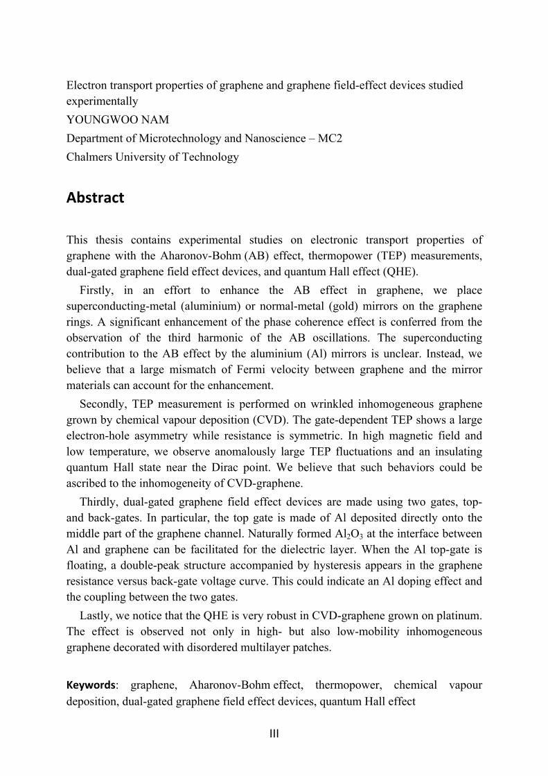
Abstract
This thesis contains experimental studies on electronic transport properties of graphene with the Aharonov-Bohm (AB) effect, thermopower (TEP) measurements, dual-gated graphene field effect devices, and quantum Hall effect (QHE).
Firstly, in an effort to enhance the AB effect in graphene, we place superconducting-metal (aluminium) or normal-metal (gold) mirrors on the graphene rings. A significant enhancement of the phase coherence effect is conferred from the observation of the third harmonic of the AB oscillations. The superconducting contribution to the AB effect by the aluminium (Al) mirrors is unclear. Instead, we believe that a large mismatch of Fermi velocity between graphene and the mirror materials can account for the enhancement.
Secondly, TEP measurement is performed on wrinkled inhomogeneous graphene grown by chemical vapour deposition (CVD). The gate-dependent TEP shows a large electron-hole asymmetry while resistance is symmetric. In high magnetic field and low temperature, we observe anomalously large TEP fluctuations and an insulating quantum Hall state near the Dirac point. We believe that such behaviors could be ascribed to the inhomogeneity of CVD-graphene.
Thirdly, dual-gated graphene field effect devices are made using two gates, top- and back-gates. In particular, the top gate is made of Al deposited directly onto the middle part of the graphene channel. Naturally formed Al2O3 at the interface between Al and graphene can be facilitated for the dielectric layer. When the Al top-gate is floating, a double-peak structure accompanied by hysteresis appears in the graphene resistance versus back-gate voltage curve. This could indicate an Al doping effect and the coupling between the two gates.
Lastly, we notice that the QHE is very robust in CVD-graphene grown on platinum. The effect is observed not only in high- but also low-mobility inhomogeneous graphene decorated with disordered multilayer patches.
Keywords: graphene, Aharonov-Bohm effect, thermopower, chemical vapour deposition, dual-gated graphene field effect devices, quantum Hall effect

IV
V
List of appended papers
This thesis is based on the work contained in the following papers:
A. The Aharonov-Bohm effect in graphene rings with metal mirrors Youngwoo Nam, Jai Seung Yoo, Yung Woo Park, Niclas Lindvall, Thilo Bauch, August Yurgens Carbon 50 (15), 5562 (2012)
B. Unusual thermopower of inhomogeneous graphene grown by chemical vapour deposition Youngwoo Nam, Jie Sun, Niclas Lindvall, Seung Jae Yang, Chong Rae Park, Yung Woo Park, August Yurgens Submitted
C. Graphene p-n-p junctions controlled by local gates made of naturally oxidized thin aluminium films Youngwoo Nam, Niclas Lindvall, Jie Sun, Yung Woo Park, August Yurgens Carbon 50 (5), 1987 (2012)
D. Quantum Hall effect in graphene decorated with disordered multilayer patches Youngwoo Nam, Jie Sun, Niclas Lindvall, Seung Jae Yang, Dmitry Kireev, Chong Rae Park, Yung Woo Park, August Yurgens Appl Phys Lett (accepted)
VI
Other papers that are outside the scope of this thesis
The following papers are not included in this thesis because they are beyond the scope of this thesis:
1. Growth mechanism of graphene on platinum: Surface catalysis and carbon segregation, Jie Sun, Youngwoo Nam, Niclas Lindvall, Matthew T. Cole, Kenneth B. K. Teo, Yung Woo Park, August Yurgens (Submitted)
2. Control of the Dirac point in graphene by UV light, August Yurgens, Niclas Lindvall, Jie Sun, Youngwoo Nam, Yung Woo Park, JETP letters (accepted)
3. Frame assisted H2O electrolysis induced H2 bubbling transfer of large area graphene grown by chemical vapor deposition on Cu, César J. Lockhart de la Rosa, Jie Sun, Niclas Lindvall, Matthew T. Cole, Youngwoo Nam, Markus Löffler, Eva Olsson, Kenneth B. K. Teo, August Yurgens, Appl Phys Lett 102, 022101 (2013)
4. Hydrogen Spillover in Pd-doped V2O5 Nanowires at Room Temperature, Byung Hoon Kim, Han Young Yu, Won G. Hong, Jonghyurk Park, Sung Chul Jung, Youngwoo Nam, Hu Young Jeong, Yung Woo Park, Yongseok Jun, Hae Jin Kim, Chemistry - An Asian Journal 7, 684 (2012)
5. Suppression of the magneto resistance in high electric fields of polyacetylene nanofibers, A. Choi, H.J. Lee, A.B. Kaiser, S.H. Jhang, S.H. Lee, J.S. Yoo, H.S. Kim, Y.W. Nam, S.J. Park, H.N. Yoo, A.N. Aleshin, M. Goh, K. Akagi, R.B. Kaner, J.S. Brooks, J. Svensson, S.A. Brazovskii, N.N. Kirova, Y.W. Park, Synth Met 160, 1349 (2010)
6. Magnetotransport in iodine-doped single-walled carbon nanotubes, Sejung Ahn, Yukyung Kim, Youngwoo Nam, Honam Yoo, Jihyun Park, Zhiyong Wang, Zujin Shi, Zhaoxia Jin, Yungwoo Park, Phys Rev B 80, 165426 (2009)
7. Temperature dependent conductivity and thermoelectric power of the iodine doped poly(vinyl alcohol)-Cu2+ chelate, Sejung Ahn, Honam Yoo, Youngwoo Nam, Jihyun Park, Yukyung Kim, Mikyong Yoo, Chongsu Cho, Yungwoo Park, Synth Met 159, 2086 (2009)
VII
Contents
Abstract ...................................................................................................................... III
List of appended papers .............................................................................................. V
Other papers that are outside the scope of this thesis ............................................ VI
1. Introduction .............................................................................................................. 9
1.1 Graphene ............................................................................................................ 9
1.2 Purpose and scope of this thesis ...................................................................... 12
2. Concepts .................................................................................................................. 13
2.1 Aharonov-Bohm (AB) effect ........................................................................... 13
2.2 Thermopower (TEP) ........................................................................................ 16
2.3 Graphene p-n-p junctions and graphene-metal contact ................................... 19
3. Experimental techniques ........................................................................................ 21
3.1 Microfabrication of graphene devices ............................................................. 21
3.2 Graphene growth by chemical vapour deposition (CVD) ............................... 23
4. The Aharonov-Bohm (AB) effect in graphene rings with metal mirrors .......... 25
4.1 Introduction ...................................................................................................... 25
4.2 AB-ring devices and experimental details ....................................................... 26
4.3 Raman spectrum and Coulomb blockade effect .............................................. 27
4.4 AB oscillations with Al T- and Al L-mirrors .................................................. 28
4.5 AB oscillations with Al L-mirrors and without mirrors .................................. 31
4.6 AB oscillations with Au T- mirrors, Au L-mirrors and without mirrors ......... 32
4.7 Conclusions ...................................................................................................... 32
5. Unusual thermopower (TEP) of inhomogeneous graphene grown by chemical vapour deposition ....................................................................................................... 35
5.1 Introduction ...................................................................................................... 35
5.2 The TEP device and experimental details ....................................................... 36
5.3 AFM and Raman mapping ............................................................................... 37
5.4 Gate voltage dependence of resistance and TEP ............................................. 38
5.5 Simulation of inhomogeneity effect using simple mesh ................................. 40
5.6 Quantum Hall effect (QHE) ............................................................................. 41
5.7 Magneto TEP ................................................................................................... 42
5.8 Conclusions ...................................................................................................... 43
VIII
6. Graphene p-n-p junctions made of naturally oxidized thin aluminium films .. 45
6.1 Introduction ...................................................................................................... 45
6.2 The graphene p-n-p device and experimental details ...................................... 46
6.3 Al oxidation at the interface with graphene ..................................................... 47
6.4 Dual-gate effect using the aluminium top gate ................................................ 48
6.5 Double-peak structure in the transfer curve when Al top gate is floating ....... 49
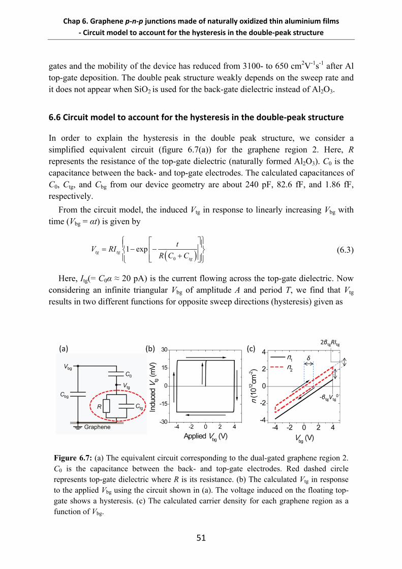
6.6 Circuit model to account for the hysteresis in the double-peak structure ....... 51
6.7 Conclusions ...................................................................................................... 53
7. Quantum Hall effect in graphene decorated with disordered multilayer patches ......................................................................................................................... 55
7.1 Introduction ...................................................................................................... 55
7.2 Graphene growth on platinum by CVD ........................................................... 56
7.3 Transfer curves and Raman mapping .............................................................. 57
7.4 Quantum Hall effect (QHE) ............................................................................. 59
7.5 Unusual ν = 0 quantum Hall state .................................................................... 61
7.6 Conclusions ...................................................................................................... 62
8. Summary ................................................................................................................. 63
Acknowledgements ..................................................................................................... 65
References .................................................................................................................... 67
Chap 1. Introduction
‐ Graphene
9
Chapter 1
1. Introduction
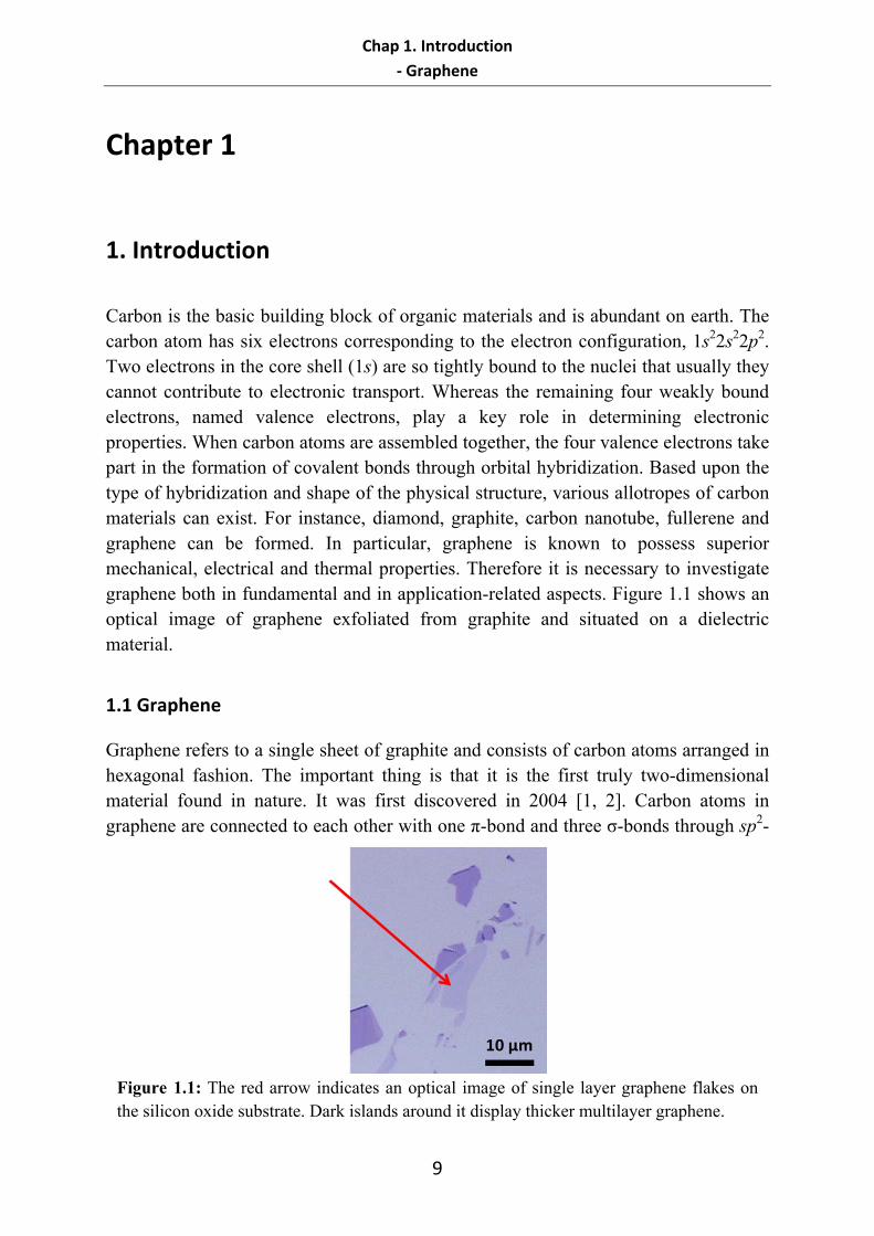
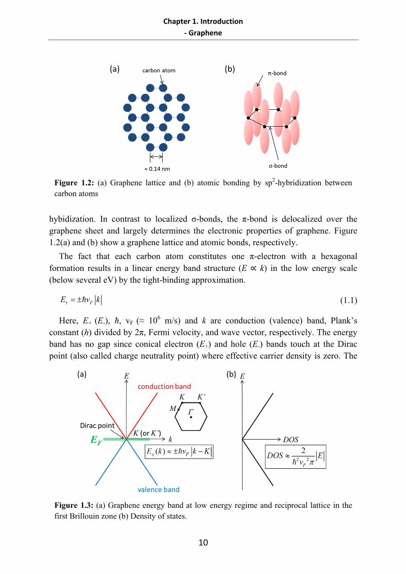
Carbon is the basic building block of organic materials and is abundant on earth. The carbon atom has six electrons corresponding to the electron configuration, 1s22s22p2. Two electrons in the core shell (1s) are so tightly bound to the nuclei that usually they cannot contribute to electronic transport. Whereas the remaining four weakly bound electrons, named valence electrons, play a key role in determining electronic properties. When carbon atoms are assembled together, the four valence electrons take part in the formation of covalent bonds through orbital hybridization. Based upon the type of hybridization and shape of the physical structure, various allotropes of carbon materials can exist. For instance, diamond, graphite, carbon nanotube, fullerene and graphene can be formed. In particular, graphene is known to possess superior mechanical, electrical and thermal properties. Therefore it is necessary to investigate graphene both in fundamental and in application-related aspects. Figure 1.1 shows an optical image of graphene exfoliated from graphite and situated on a dielectric material.
1.1 Graphene
Graphene refers to a single sheet of graphite and consists of carbon atoms arranged in hexagonal fashion. The important thing is that it is the first truly two-dimensional material found in nature. It was first discovered in 2004 [1, 2]. Carbon atoms in graphene are connected to each other with one π-bond and three σ-bonds through sp2-
Figure 1.1: The red arrow indicates an optical image of single layer graphene flakes on the silicon oxide substrate. Dark islands around it display thicker multilayer graphene.
Chapter 1. Introduction
‐ Graphene
10
hybidization. In contrast to localized σ-bonds, the π-bond is delocalized over the graphene sheet and largely determines the electronic properties of graphene. Figure 1.2(a) and (b) show a graphene lattice and atomic bonds, respectively.
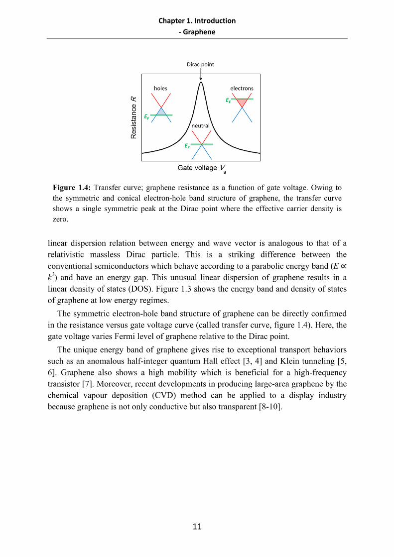
The fact that each carbon atom constitutes one π-electron with a hexagonal formation results in a linear energy band structure (E ∝ k) in the low energy scale (below several eV) by the tight-binding approximation.
FE v k (1.1)
Here, E+ (E-), ħ, vF (≈ 106 m/s) and k are conduction (valence) band, Plank’s constant (h) divided by 2π, Fermi velocity, and wave vector, respectively. The energy band has no gap since conical electron (E+) and hole (E-) bands touch at the Dirac point (also called charge neutrality point) where effective carrier density is zero. The
Figure 1.2: (a) Graphene lattice and (b) atomic bonding by sp2-hybridization between carbon atoms
Figure 1.3: (a) Graphene energy band at low energy regime and reciprocal lattice in the first Brillouin zone (b) Density of states.
Chapter 1. Introduction
‐ Graphene
11
linear dispersion relation between energy and wave vector is analogous to that of a relativistic massless Dirac particle. This is a striking difference between the conventional semiconductors which behave according to a parabolic energy band (E ∝ k2) and have an energy gap. This unusual linear dispersion of graphene results in a linear density of states (DOS). Figure 1.3 shows the energy band and density of states of graphene at low energy regimes.
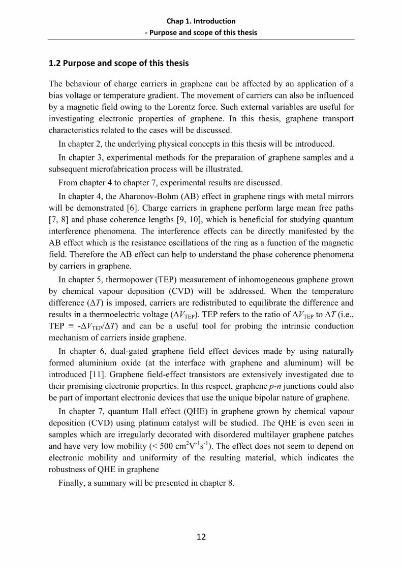
The symmetric electron-hole band structure of graphene can be directly confirmed in the resistance versus gate voltage curve (called transfer curve, figure 1.4). Here, the gate voltage varies Fermi level of graphene relative to the Dirac point.
The unique energy band of graphene gives rise to exceptional transport behaviors such as an anomalous half-integer quantum Hall effect [3, 4] and Klein tunneling [5, 6]. Graphene also shows a high mobility which is beneficial for a high-frequency transistor [7]. Moreover, recent developments in producing large-area graphene by the chemical vapour deposition (CVD) method can be applied to a display industry because graphene is not only conductive but also transparent [8-10].
Figure 1.4: Transfer curve; graphene resistance as a function of gate voltage. Owing to the symmetric and conical electron-hole band structure of graphene, the transfer curve shows a single symmetric peak at the Dirac point where the effective carrier density is zero.
Chap 1. Introduction
‐ Purpose and scope of this thesis
12
1.2 Purpose and scope of this thesis
The behaviour of charge carriers in graphene can be affected by an application of a bias voltage or temperature gradient. The movement of carriers can also be influenced by a magnetic field owing to the Lorentz force. Such external variables are useful for investigating electronic properties of graphene. In this thesis, graphene transport characteristics related to the cases will be discussed.
In chapter 2, the underlying physical concepts in this thesis will be introduced.
In chapter 3, experimental methods for the preparation of graphene samples and a subsequent microfabrication process will be illustrated.
From chapter 4 to chapter 7, experimental results are discussed.
In chapter 4, the Aharonov-Bohm (AB) effect in graphene rings with metal mirrors will be demonstrated [6]. Charge carriers in graphene perform large mean free paths [7, 8] and phase coherence lengths [9, 10], which is beneficial for studying quantum interference phenomena. The interference effects can be directly manifested by the AB effect which is the resistance oscillations of the ring as a function of the magnetic field. Therefore the AB effect can help to understand the phase coherence phenomena by carriers in graphene.
In chapter 5, thermopower (TEP) measurement of inhomogeneous graphene grown by chemical vapour deposition (CVD) will be addressed. When the temperature difference (ΔT) is imposed, carriers are redistributed to equilibrate the difference and results in a thermoelectric voltage (ΔVTEP). TEP refers to the ratio of ΔVTEP to ΔT (i.e., TEP ≡ -ΔVTEP/ΔT) and can be a useful tool for probing the intrinsic conduction mechanism of carriers inside graphene.
In chapter 6, dual-gated graphene field effect devices made by using naturally formed aluminium oxide (at the interface with graphene and aluminum) will be introduced [11]. Graphene field-effect transistors are extensively investigated due to their promising electronic properties. In this respect, graphene p-n junctions could also be part of important electronic devices that use the unique bipolar nature of graphene.
In chapter 7, quantum Hall effect (QHE) in graphene grown by chemical vapour deposition (CVD) using platinum catalyst will be studied. The QHE is even seen in samples which are irregularly decorated with disordered multilayer graphene patches and have very low mobility (< 500 cm2V-1s-1). The effect does not seem to depend on electronic mobility and uniformity of the resulting material, which indicates the robustness of QHE in graphene
Finally, a summary will be presented in chapter 8.
Chap 2. Concepts
‐ Aharonov‐Bohm (AB) effect
13
Chapter 2
2. Concepts
2.1 Aharonov‐Bohm (AB) effect
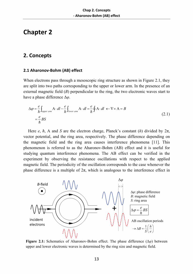
When electrons pass through a mesoscopic ring structure as shown in Figure 2.1, they are split into two paths corresponding to the upper or lower arm. In the presence of an external magnetic field (B) perpendicular to the ring, the two electronic waves start to have a phase difference Δφ.
upper arm lower arm
e e edl dl dl B
eBS
(2.1)
Here e, ħ, Α and S are the electron charge, Planck’s constant (h) divided by 2π, vector potential, and the ring area, respectively. The phase difference depending on the magnetic field and the ring area causes interference phenomena [11]. This phenomenon is referred to as the Aharonov-Bohm (AB) effect and it is useful for studying quantum interference phenomena. The AB effect can be verified in the experiment by observing the resistance oscillations with respect to the applied magnetic field. The periodicity of the oscillation corresponds to the case whenever the phase difference is a multiple of 2π, which is analogous to the interference effect in
Figure 2.1: Schematics of Aharonov-Bohm effect. The phase difference (Δφ) between upper and lower electronic waves is determined by the ring size and magnetic field.
Chap 2. Concepts
‐ Aharonov‐Bohm (AB) effect
14
the double slit experiment with light.
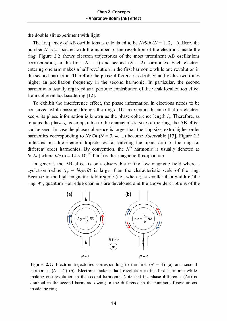
The frequency of AB oscillations is calculated to be NeS/h (N = 1, 2, ...). Here, the number N is associated with the number of the revolution of the electrons inside the ring. Figure 2.2 shows electron trajectories of the most prominent AB oscillations corresponding to the first (N = 1) and second (N = 2) harmonics. Each electron entering one arm makes a half revolution in the first harmonic while one revolution in the second harmonic. Therefore the phase difference is doubled and yields two times higher an oscillation frequency in the second harmonic. In particular, the second harmonic is usually regarded as a periodic contribution of the weak localization effect from coherent backscattering [12].
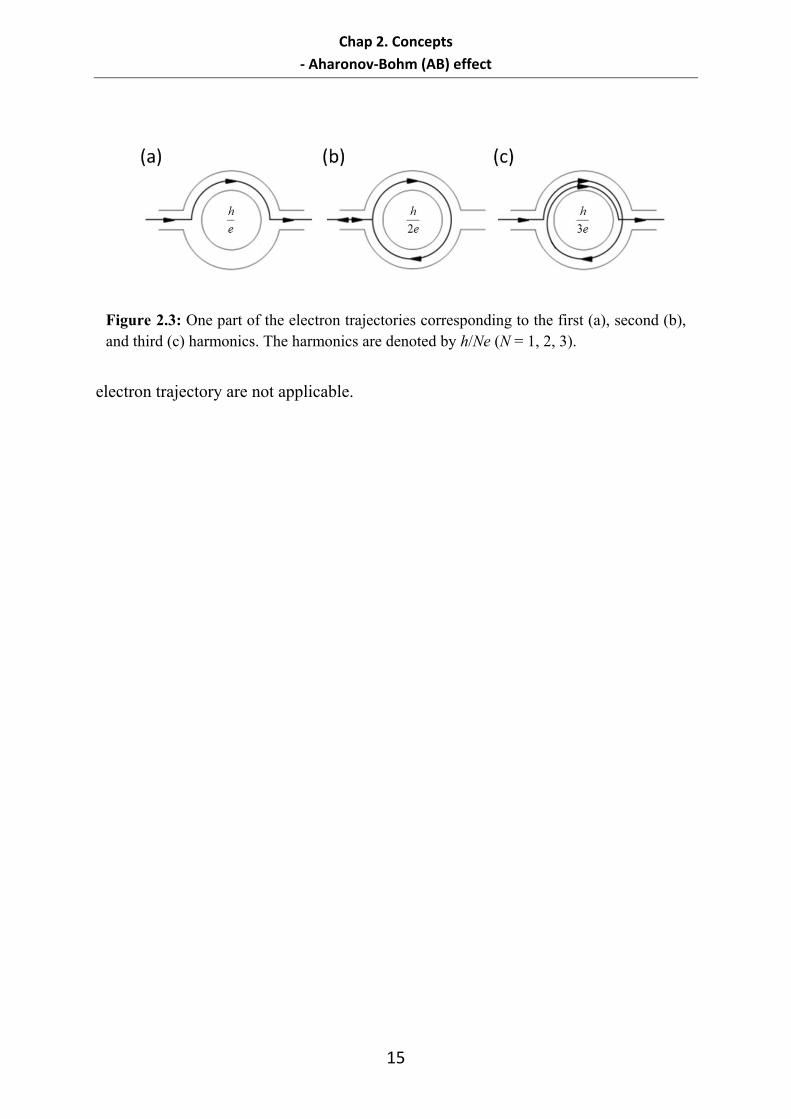
To exhibit the interference effect, the phase information in electrons needs to be conserved while passing through the rings. The maximum distance that an electron keeps its phase information is known as the phase coherence length lφ. Therefore, as long as the phase lφ is comparable to the characteristic size of the ring, the AB effect can be seen. In case the phase coherence is larger than the ring size, extra higher order harmonics corresponding to NeS/h (N = 3, 4, ...) become observable [13]. Figure 2.3 indicates possible electron trajectories for entering the upper arm of the ring for different order harmonics. By convention, the Nth harmonic is usually denoted as h/(Ne) where h/e (≈ 4.14 × 10⁻¹⁵ T·m2) is the magnetic flux quantum.
In general, the AB effect is only observable in the low magnetic field where a cyclotron radius (rc = ħkF/eB) is larger than the characteristic scale of the ring. Because in the high magnetic field regime (i.e., when rc is smaller than width of the ring W), quantum Hall edge channels are developed and the above descriptions of the
Figure 2.2: Electron trajectories corresponding to the first (N = 1) (a) and second harmonics (N = 2) (b). Electrons make a half revolution in the first harmonic while making one revolution in the second harmonic. Note that the phase difference (Δφ) is doubled in the second harmonic owing to the difference in the number of revolutions inside the ring.
Chap 2. Concepts
‐ Aharonov‐Bohm (AB) effect
15
electron trajectory are not applicable.
Figure 2.3: One part of the electron trajectories corresponding to the first (a), second (b), and third (c) harmonics. The harmonics are denoted by h/Ne (N = 1, 2, 3).
Chap 2. Concepts
‐ Thermopower (TEP)
16
2.2 Thermopower (TEP)
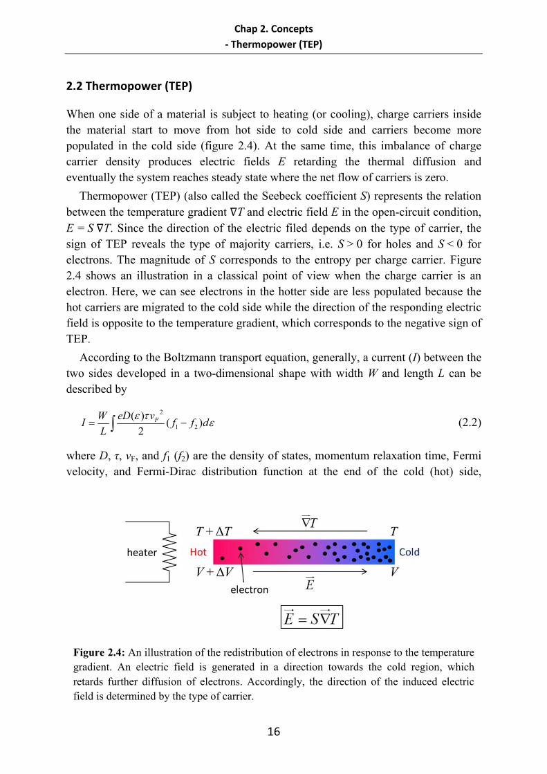
When one side of a material is subject to heating (or cooling), charge carriers inside the material start to move from hot side to cold side and carriers become more populated in the cold side (figure 2.4). At the same time, this imbalance of charge carrier density produces electric fields E retarding the thermal diffusion and eventually the system reaches steady state where the net flow of carriers is zero.
Thermopower (TEP) (also called the Seebeck coefficient S) represents the relation between the temperature gradient T and electric field E in the open-circuit condition, E = S T. Since the direction of the electric filed depends on the type of carrier, the sign of TEP reveals the type of majority carriers, i.e. S > 0 for holes and S < 0 for electrons. The magnitude of S corresponds to the entropy per charge carrier. Figure 2.4 shows an illustration in a classical point of view when the charge carrier is an electron. Here, we can see electrons in the hotter side are less populated because the hot carriers are migrated to the cold side while the direction of the responding electric field is opposite to the temperature gradient, which corresponds to the negative sign of TEP.
According to the Boltzmann transport equation, generally, a current (I) between the two sides developed in a two-dimensional shape with width W and length L can be described by
2
1 2
( )( )
2FeD vW
I f f dL
(2.2)
where D, τ, vF, and f1 (f2) are the density of states, momentum relaxation time, Fermi velocity, and Fermi-Dirac distribution function at the end of the cold (hot) side,
Figure 2.4: An illustration of the redistribution of electrons in response to the temperature gradient. An electric field is generated in a direction towards the cold region, which retards further diffusion of electrons. Accordingly, the direction of the induced electric field is determined by the type of carrier.
Chap 2. Concepts
‐ Thermopower (TEP)
17
respectively.
By using series expansion of f1- f2 this can by approximated as
1 2( , ) ( , ) Fff T f e V T T e V T
T
(2.3)
and employing the open circuit condition, I = 0. TEP (S) is given by
( ) '( )1
'( )
1
F
F
fd
VS
fT eT d
eT
where 2 2( )
'( )2
Fe D v (2.4)
Here, εF and σ’(ε) are Fermi energy and energy-dependent partial conductivity of the
total conductivity (σ) (i.e., / '( )f d ).
From the Sommerfeld expansion, the TEP formula in eq. 2.4 can be expressed in terms of total conductivity σ (called Mott relation) as
2 1when 1
3B B
Mott BF
k k TS k T
e
(2.5)
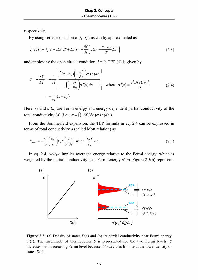
In eq. 2.4, <ε-εF> implies averaged energy relative to the Fermi energy, which is weighted by the partial conductivity near Fermi energy σ’(ε). Figure 2.5(b) represents
Figure 2.5: (a) Density of states D(ε) and (b) its partial conductivity near Fermi energy σ’(ε). The magnitude of thermopower S is represented for the two Fermi levels. S increases with decreasing Fermi level because <ε> deviates from εF at the lower density of states D(ε).
Chap 2. Concepts
‐ Thermopower (TEP)
18
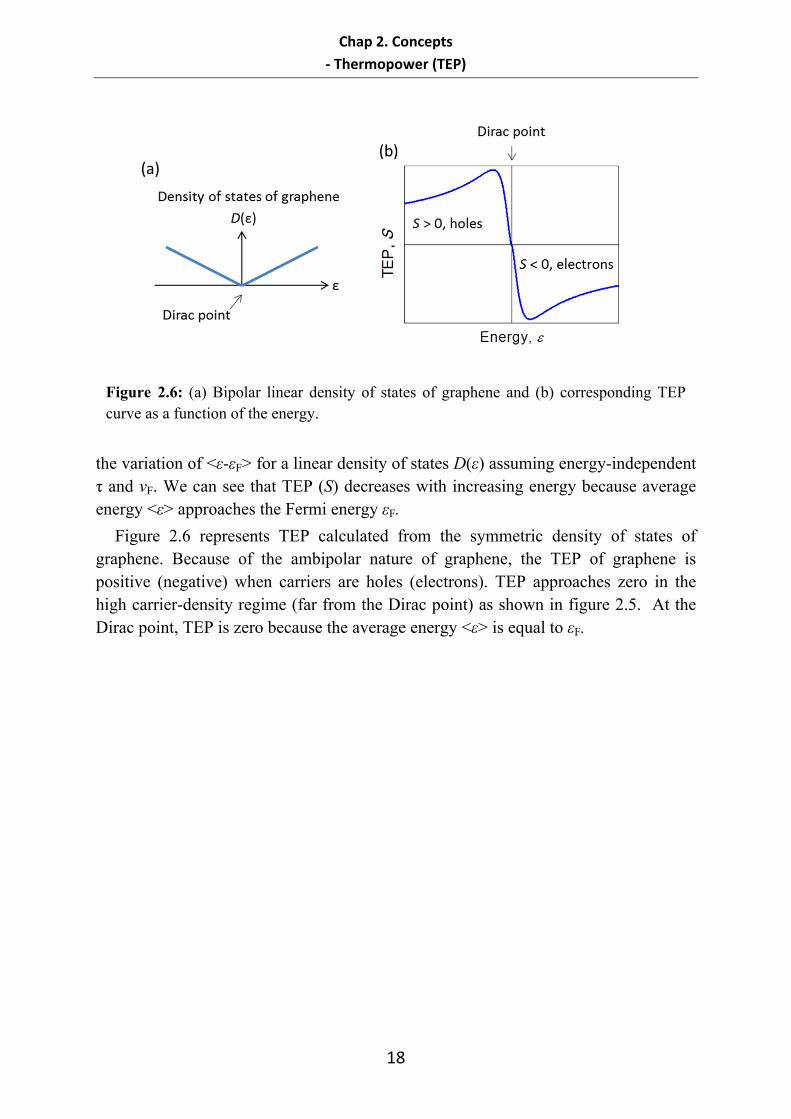
the variation of <ε-εF> for a linear density of states D(ε) assuming energy-independent τ and vF. We can see that TEP (S) decreases with increasing energy because average energy <ε> approaches the Fermi energy εF.
Figure 2.6 represents TEP calculated from the symmetric density of states of graphene. Because of the ambipolar nature of graphene, the TEP of graphene is positive (negative) when carriers are holes (electrons). TEP approaches zero in the high carrier-density regime (far from the Dirac point) as shown in figure 2.5. At the Dirac point, TEP is zero because the average energy <ε> is equal to εF.
Figure 2.6: (a) Bipolar linear density of states of graphene and (b) corresponding TEP curve as a function of the energy.
Chap 2. Concepts
‐ Graphene p‐n‐p junctions and graphene‐metal contact
19
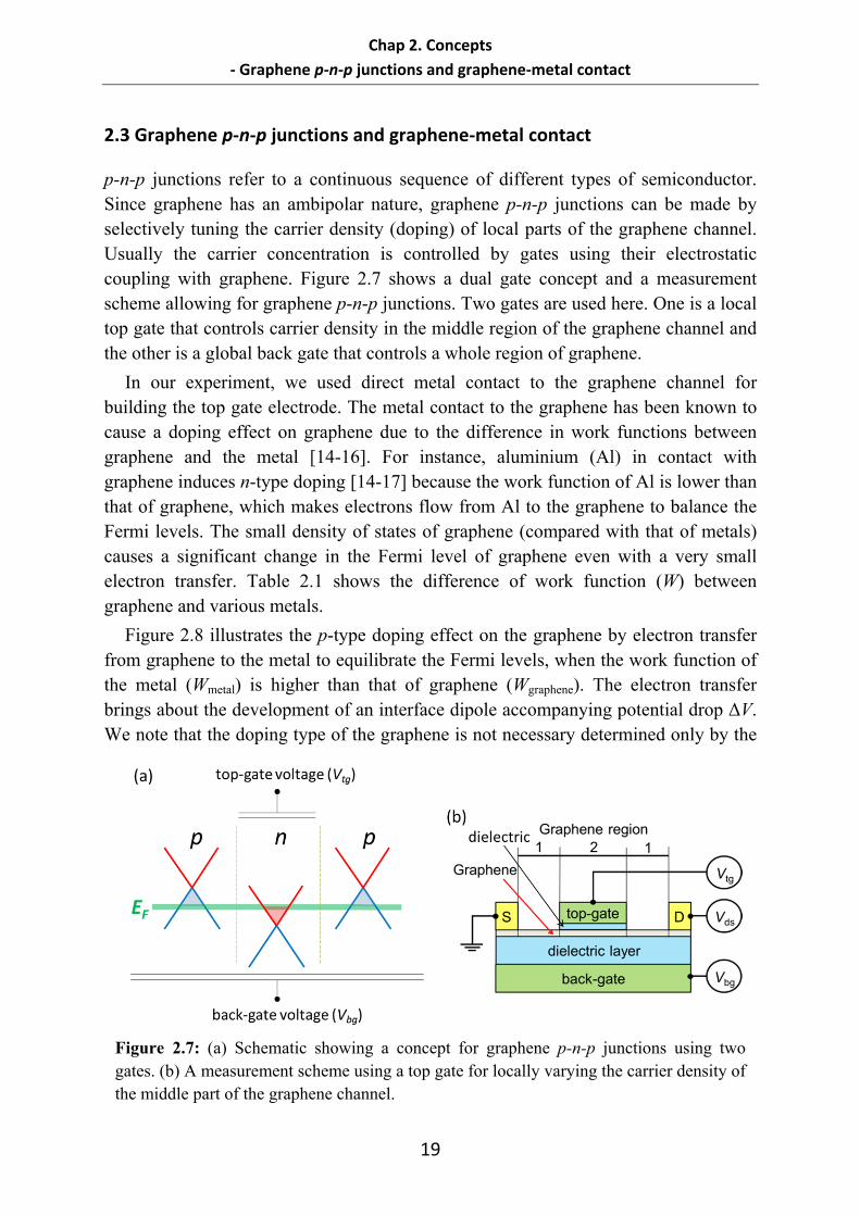
2.3 Graphene p‐n‐p junctions and graphene‐metal contact
p-n-p junctions refer to a continuous sequence of different types of semiconductor. Since graphene has an ambipolar nature, graphene p-n-p junctions can be made by selectively tuning the carrier density (doping) of local parts of the graphene channel. Usually the carrier concentration is controlled by gates using their electrostatic coupling with graphene. Figure 2.7 shows a dual gate concept and a measurement scheme allowing for graphene p-n-p junctions. Two gates are used here. One is a local top gate that controls carrier density in the middle region of the graphene channel and the other is a global back gate that controls a whole region of graphene.
In our experiment, we used direct metal contact to the graphene channel for building the top gate electrode. The metal contact to the graphene has been known to cause a doping effect on graphene due to the difference in work functions between graphene and the metal [14-16]. For instance, aluminium (Al) in contact with graphene induces n-type doping [14-17] because the work function of Al is lower than that of graphene, which makes electrons flow from Al to the graphene to balance the Fermi levels. The small density of states of graphene (compared with that of metals) causes a significant change in the Fermi level of graphene even with a very small electron transfer. Table 2.1 shows the difference of work function (W) between graphene and various metals.
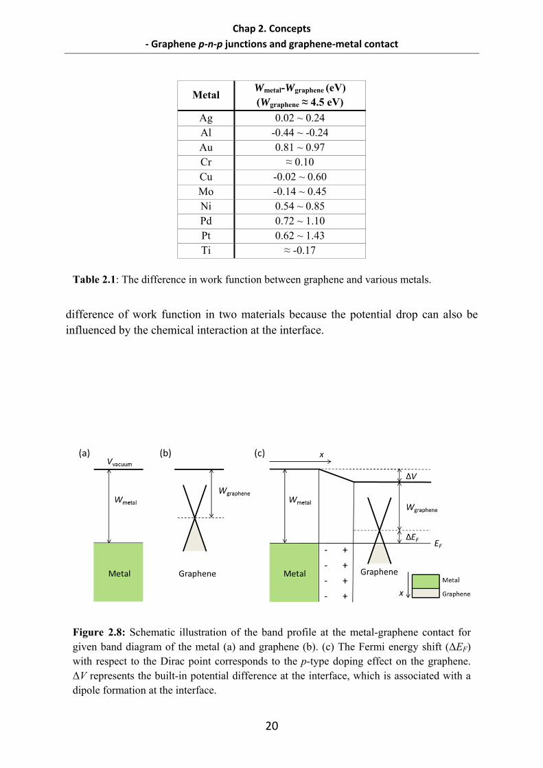
Figure 2.8 illustrates the p-type doping effect on the graphene by electron transfer from graphene to the metal to equilibrate the Fermi levels, when the work function of the metal (Wmetal) is higher than that of graphene (Wgraphene). The electron transfer brings about the development of an interface dipole accompanying potential drop ΔV. We note that the doping type of the graphene is not necessary determined only by the
Figure 2.7: (a) Schematic showing a concept for graphene p-n-p junctions using two gates. (b) A measurement scheme using a top gate for locally varying the carrier density of the middle part of the graphene channel.
Chap 2. Concepts
‐ Graphene p‐n‐p junctions and graphene‐metal contact
20
difference of work function in two materials because the potential drop can also be influenced by the chemical interaction at the interface.
Metal Wmetal-Wgraphene (eV) (Wgraphene ≈ 4.5 eV)
Ag 0.02 ~ 0.24 Al -0.44 ~ -0.24 Au 0.81 ~ 0.97 Cr ≈ 0.10 Cu -0.02 ~ 0.60 Mo -0.14 ~ 0.45 Ni 0.54 ~ 0.85 Pd 0.72 ~ 1.10 Pt 0.62 ~ 1.43 Ti ≈ -0.17
Table 2.1: The difference in work function between graphene and various metals.
Figure 2.8: Schematic illustration of the band profile at the metal-graphene contact for given band diagram of the metal (a) and graphene (b). (c) The Fermi energy shift (ΔEF) with respect to the Dirac point corresponds to the p-type doping effect on the graphene. ΔV represents the built-in potential difference at the interface, which is associated with a dipole formation at the interface.
Chap 3. Experimental techniques
‐ Microfabrication of graphene devices
21
Chapter 3
3. Experimental techniques
3.1 Microfabrication of graphene devices
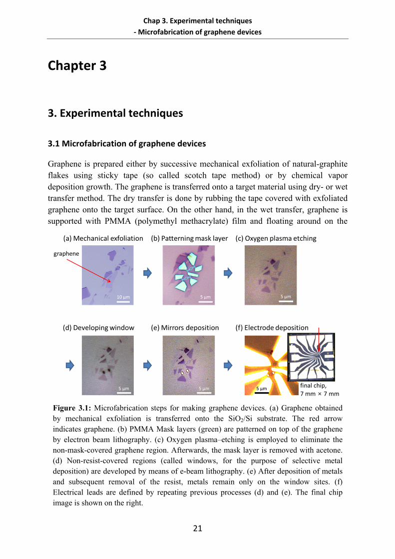
Graphene is prepared either by successive mechanical exfoliation of natural-graphite flakes using sticky tape (so called scotch tape method) or by chemical vapor deposition growth. The graphene is transferred onto a target material using dry- or wet transfer method. The dry transfer is done by rubbing the tape covered with exfoliated graphene onto the target surface. On the other hand, in the wet transfer, graphene is supported with PMMA (polymethyl methacrylate) film and floating around on the
Figure 3.1: Microfabrication steps for making graphene devices. (a) Graphene obtained by mechanical exfoliation is transferred onto the SiO2/Si substrate. The red arrow indicates graphene. (b) PMMA Mask layers (green) are patterned on top of the graphene by electron beam lithography. (c) Oxygen plasma–etching is employed to eliminate the non-mask-covered graphene region. Afterwards, the mask layer is removed with acetone. (d) Non-resist-covered regions (called windows, for the purpose of selective metal deposition) are developed by means of e-beam lithography. (e) After deposition of metals and subsequent removal of the resist, metals remain only on the window sites. (f) Electrical leads are defined by repeating previous processes (d) and (e). The final chip image is shown on the right.
Chap 3. Experimental techniques
‐ Microfabrication of graphene devices
22
distilled water. Then this is snatched with the target material by immersing it into the distilled water. In our experiments, the target materials are heavily doped silicon substrate (acting as a gate electrode) capped with 300 nm-thick SiO2 or 89 nm-thick Al2O3 dielectric layer. These thicknesses of SiO2 and Al2O3 provide a good contrast for seeing graphene with an optical microscope [18-21].
Afterwards, to make the desired shape of graphene, oxygen plasma-etching is applied to the graphene coated with an e-beam patterned PMMA mask. Consecutively, metal contacts to the graphene are defined by thermally evaporating thin metal films onto the e-beam patterned region. Figure 3.1 displays the detailed process of the microfabrication.
Chap 3. Experimental techniques
‐ Graphene growth by chemical vapour deposition (CVD)
23
3.2 Graphene growth by chemical vapour deposition (CVD)
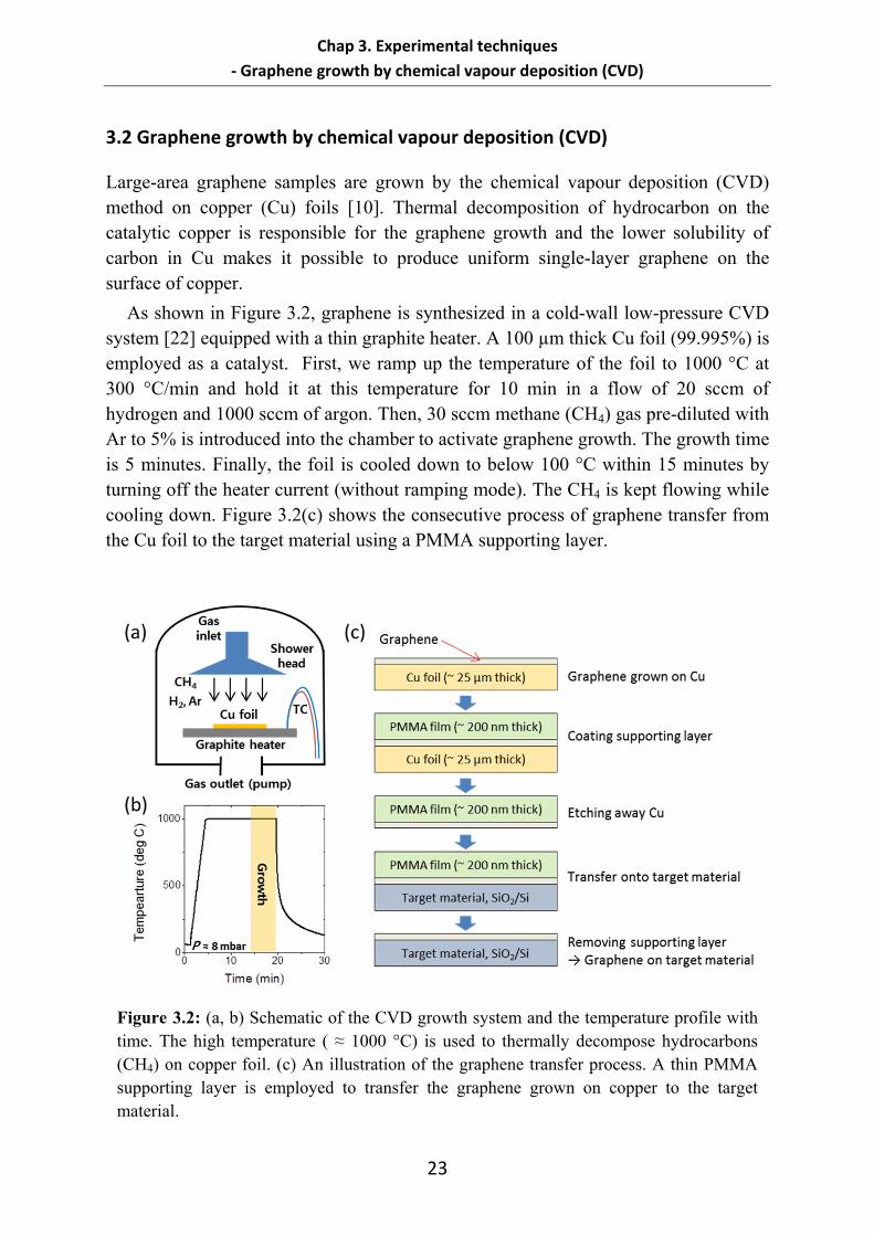
Large-area graphene samples are grown by the chemical vapour deposition (CVD) method on copper (Cu) foils [10]. Thermal decomposition of hydrocarbon on the catalytic copper is responsible for the graphene growth and the lower solubility of carbon in Cu makes it possible to produce uniform single-layer graphene on the surface of copper.
As shown in Figure 3.2, graphene is synthesized in a cold-wall low-pressure CVD system [22] equipped with a thin graphite heater. A 100 µm thick Cu foil (99.995%) is employed as a catalyst. First, we ramp up the temperature of the foil to 1000 °C at 300 °C/min and hold it at this temperature for 10 min in a flow of 20 sccm of hydrogen and 1000 sccm of argon. Then, 30 sccm methane (CH4) gas pre-diluted with Ar to 5% is introduced into the chamber to activate graphene growth. The growth time is 5 minutes. Finally, the foil is cooled down to below 100 °C within 15 minutes by turning off the heater current (without ramping mode). The CH4 is kept flowing while cooling down. Figure 3.2(c) shows the consecutive process of graphene transfer from the Cu foil to the target material using a PMMA supporting layer.
Figure 3.2: (a, b) Schematic of the CVD growth system and the temperature profile with time. The high temperature ( ≈ 1000 °C) is used to thermally decompose hydrocarbons (CH4) on copper foil. (c) An illustration of the graphene transfer process. A thin PMMA supporting layer is employed to transfer the graphene grown on copper to the target material.
Chap 3. Experimental techniques
‐ Microfabrication of graphene devices
24
Chap 4. The Aharonov‐Bohm (AB) effect in graphene rings with metal mirrors
‐ Introduction
25
Chapter 4
4. The Aharonov‐Bohm (AB) effect in graphene rings with
metal mirrors
4.1 Introduction
The Aharonov-Bohm (AB) effect is beneficial for investigating quantum interference behaviour in graphene [11] because it directly shows the interference effects by resistance oscillations of a ring as a function of the magnetic field. The oscillations arise from the phase difference between the electrons passing through the two different arms of the ring.
Usually, the experimentally observable frequencies (=NeS/h) of the AB oscillations are the first (N=1) and second (N=2) harmonics, where e, S, and h are the electron charge, the ring area, and Plank’s constant, respectively [11]. In principle, the amount by which the maximum distance that an electron keeps its phase information (phase coherence length, lφ) is larger than the size of the ring, the more higher order harmonics (N = 3, 4, ...) become available [23].
Graphene can be a suitable material for the AB experiment because carriers in graphene demonstrate large mean free paths and phase coherence lengths [24, 25]. So far, a number of groups have reported the AB experiment with graphene [26-30]. However, the AB oscillation signal was weak and up to 2nd harmonics appeared. One method to enhance the visibility of the AB effect is to utilize either superconducting [12, 31] or normal metal mirrors [32]. Andreev reflection by superconducting mirrors [12, 31] and Fermi velocity mismatch [32] between mirrors and graphene could
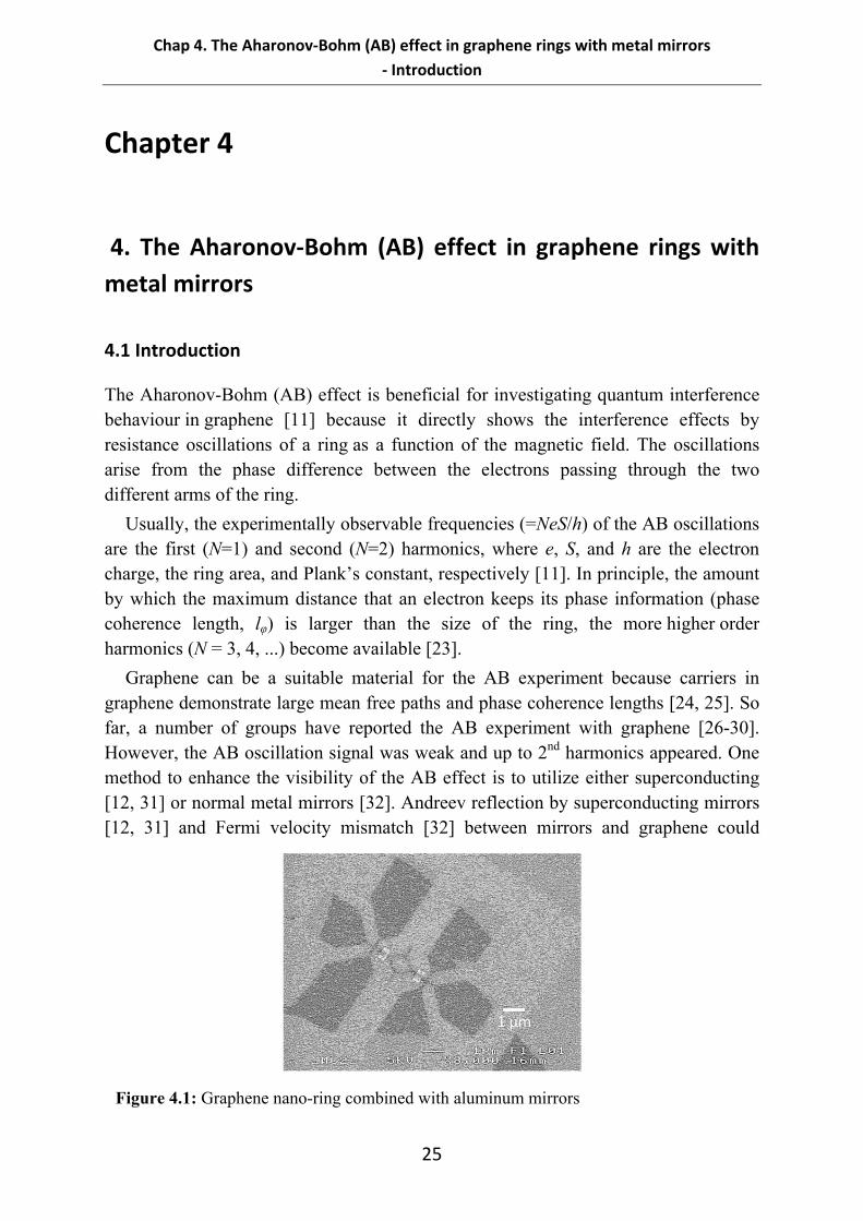
Figure 4.1: Graphene nano-ring combined with aluminum mirrors
Chap 4. The Aharonov‐Bohm (AB) effect in graphene rings with metal mirrors
‐ AB‐ring devices and experimental details
26
account for the enhancement.
We present the AB effect in the graphene ring structure (AB-ring) deposited with two materials; 1) superconducting and 2) normal metal mirrors. In particular, we observe the third harmonic (3eS/h) of the AB oscillations with superconducting mirrors deposited in the ring bias line. However, the contribution from the superconducting effect is unclear because normal metal mirrors also result in the enhancement of the AB effect. Additionally, a Coulomb gap is seen near the Dirac point due to the narrowness of the AB-ring.
4.2 AB‐ring devices and experimental details
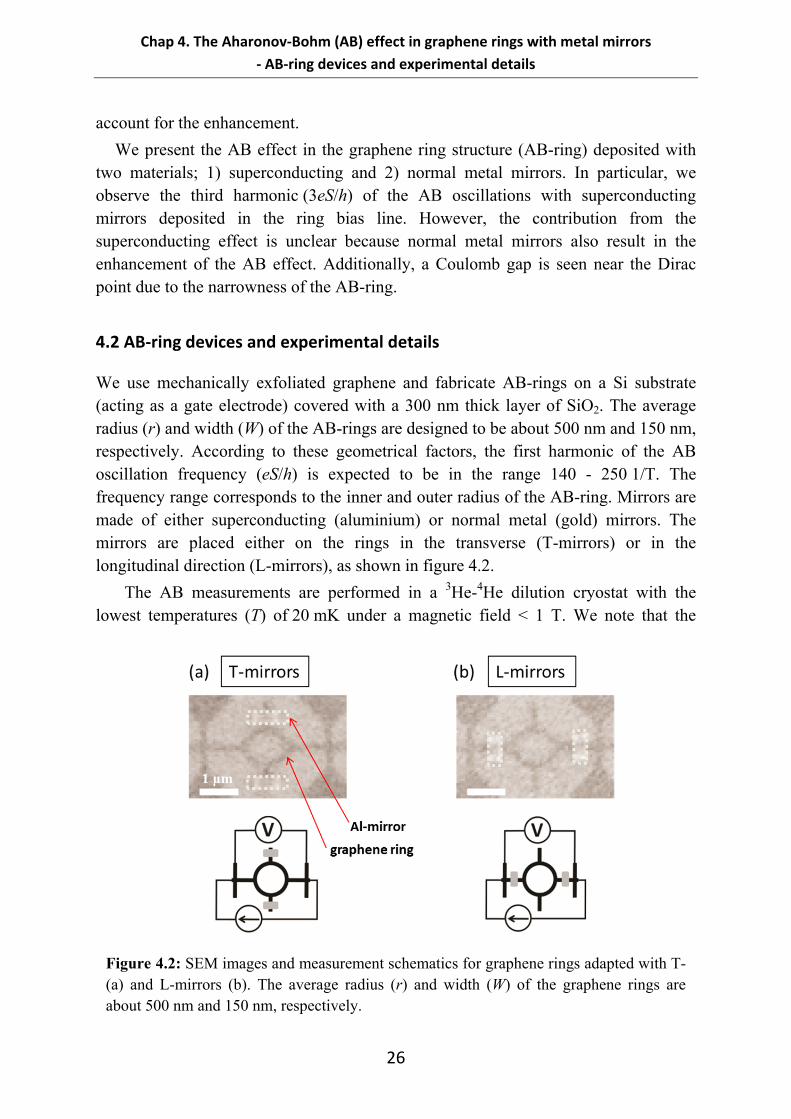
We use mechanically exfoliated graphene and fabricate AB-rings on a Si substrate (acting as a gate electrode) covered with a 300 nm thick layer of SiO2. The average radius (r) and width (W) of the AB-rings are designed to be about 500 nm and 150 nm, respectively. According to these geometrical factors, the first harmonic of the AB oscillation frequency (eS/h) is expected to be in the range 140 - 250 1/T. The frequency range corresponds to the inner and outer radius of the AB-ring. Mirrors are made of either superconducting (aluminium) or normal metal (gold) mirrors. The mirrors are placed either on the rings in the transverse (T-mirrors) or in the longitudinal direction (L-mirrors), as shown in figure 4.2.
The AB measurements are performed in a 3He-4He dilution cryostat with the lowest temperatures (T) of 20 mK under a magnetic field < 1 T. We note that the
Figure 4.2: SEM images and measurement schematics for graphene rings adapted with T- (a) and L-mirrors (b). The average radius (r) and width (W) of the graphene rings are about 500 nm and 150 nm, respectively.
Chap 4. The Aharonov‐Bohm (AB) effect in graphene rings with metal mirrors
‐ Raman spectrum and Coulomb blockade effect
27
temperature is largely lower compared to previous works on the AB effect in graphene [26-28]. The four-probe resistance measurement is performed using a low-frequency lock-in technique. In order to avoid a thermal smearing effect, the applied bias current is controlled to make the voltage across the samples lower than kBT/e.
4.3 Raman spectrum and Coulomb blockade effect
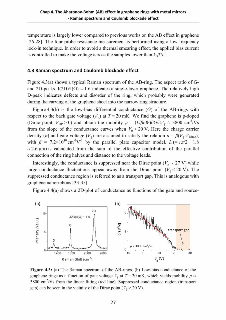
Figure 4.3(a) shows a typical Raman spectrum of the AB-ring. The aspect ratio of G- and 2D-peaks, I(2D)/I(G) ≈ 1.6 indicates a single-layer graphene. The relatively high D-peak indicates defects and disorder of the ring, which probably were generated during the carving of the graphene sheet into the narrow ring structure.
Figure 4.3(b) is the low-bias differential conductance (G) of the AB-rings with respect to the back gate voltage (Vg) at T = 20 mK. We find the graphene is p-doped (Dirac point, VDP > 0) and obtain the mobility µ = (L/βeW)∂G/∂Vg ≈ 3800 cm2/Vs from the slope of the conductance curves when Vg < 20 V. Here the charge carrier density (n) and gate voltage (Vg) are assumed to satisfy the relation n = β(Vg-VDirac), with β = 7.2×1010 cm-2V-1 by the parallel plate capacitor model. L (= rπ/2 + 1.8 ≈ 2.6 μm) is calculated from the sum of the effective contribution of the parallel connection of the ring halves and distance to the voltage leads.
Interestingly, the conductance is suppressed near the Dirac point (Vg ∼ 27 V) while large conductance fluctuations appear away from the Dirac point (Vg < 20 V). The suppressed conductance region is referred to as a transport gap. This is analogous with graphene nanoribbons [33-35].
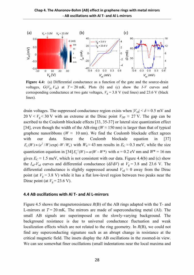
Figure 4.4(a) shows a 2D-plot of conductance as functions of the gate and source-
Figure 4.3: (a) The Raman spectrum of the AB-rings. (b) Low-bias conductance of the graphene rings as a function of gate voltage Vg at T = 20 mK, which yields mobility µ ≈ 3800 cm2/Vs from the linear fitting (red line). Suppressed conductance region (transport gap) can be seen in the vicinity of the Dirac point (Vg > 20 V).
Chap 4. The Aharonov‐Bohm (AB) effect in graphene rings with metal mirrors
‐ AB oscillations with Al T‐ and Al L‐mirrors
28
drain voltages. The suppressed conductance region exists when |Vsd| < δ ≈ 0.5 mV and 20 V < Vg < 30 V with an extreme at the Dirac point VDP ≈ 27 V. The gap can be ascribed to the Coulomb blockade effects [33, 35-37] or lateral size quantization effect [34], even though the width of the AB-ring (W ≈ 150 nm) is larger than that of typical graphene nanoribbons (W ≈ 10 nm). We find the Coulomb blockade effect agrees with our data. Since the Coulomb blockade equation in [37]
2C 0( ) ( / ) exp( / )E W e W W W with W0 ≈ 43 nm results in EC ≈ 0.3 meV, while the size
quantization equation in [34] 1C ( ) ( *)E W W W with α = 0.2 eV nm and W* = 16 nm
gives EC ≈ 1.5 meV, which is not consistent with our data. Figure 4.4(b) and (c) show the Isd-Vsd curves and differential conductance (dI/dV) at Vg = 3.8 and 23.6 V. The differential conductance is slightly suppressed around Vsd ≈ 0 away from the Dirac point (at Vg = 3.8 V) while it has a flat low-level region between two peaks near the Dirac point (at Vg = 23.6 V).
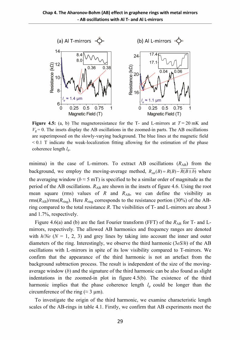
4.4 AB oscillations with Al T‐ and Al L‐mirrors
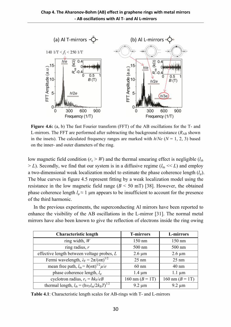
Figure 4.5 shows the magnetoresistance R(B) of the AB rings adapted with the T- and L-mirrors at T = 20 mK. The mirrors are made of superconducting metal (Al). The small AB signals are superimposed on the slowly-varying background. The background resistance is due to universal conductance fluctuation and weak localization effects which are not related to the ring geometry. In R(B), we could not find any superconducting signature such as an abrupt change in resistance at the critical magnetic field. The insets display the AB oscillations in the zoomed-in view. We can see somewhat finer oscillations (small indentations near the local maxima and
Figure 4.4: (a) Differential conductance as a function of the gate and the source-drain voltages, G(Vg, Vsd) at T = 20 mK. Plots (b) and (c) show the I-V curves and corresponding conductance at two gate voltages, Vg = 3.8 V (red lines) and 23.6 V (black lines).
Chap 4. The Aharonov‐Bohm (AB) effect in graphene rings with metal mirrors
‐ AB oscillations with Al T‐ and Al L‐mirrors
29
minima) in the case of L-mirrors. To extract AB oscillations (RAB) from the
background, we employ the moving-average method, where
the averaging window (b ≈ 5 mT) is specified to be a similar order of magnitude as the period of the AB oscillations. RAB are shown in the insets of figure 4.6. Using the root mean square (rms) values of R and RAB, we can define the visibility as rms(RAB)/rms(Rring). Here Rring corresponds to the resistance portion (30%) of the AB-ring compared to the total resistance R. The visibilities of T- and L-mirrors are about 3 and 1.7%, respectively.
Figure 4.6(a) and (b) are the fast Fourier transform (FFT) of the RAB for T- and L-mirrors, respectively. The allowed AB harmonics and frequency ranges are denoted with h/Ne (N = 1, 2, 3) and grey lines by taking into account the inner and outer diameters of the ring. Interestingly, we observe the third harmonic (3eS/h) of the AB oscillations with L-mirrors in spite of its low visibility compared to T-mirrors. We confirm that the appearance of the third harmonic is not an artefact from the background subtraction process. The result is independent of the size of the moving-average window (b) and the signature of the third harmonic can be also found as slight indentations in the zoomed-in plot in figure 4.5(b). The existence of the third harmonic implies that the phase coherence length lφ could be longer than the circumference of the ring (≈ 3 µm).
To investigate the origin of the third harmonic, we examine characteristic length scales of the AB-rings in table 4.1. Firstly, we confirm that AB experiments meet the
AB( ) ( ) ( )R B R B R B b
Figure 4.5: (a, b) The magnetoresistance for the T- and L-mirrors at T = 20 mK and Vg = 0. The insets display the AB oscillations in the zoomed-in parts. The AB oscillations are superimposed on the slowly-varying background. The blue lines at the magnetic field < 0.1 T indicate the weak-localization fitting allowing for the estimation of the phase coherence length lφ.
Chap 4. The Aharonov‐Bohm (AB) effect in graphene rings with metal mirrors
‐ AB oscillations with Al T‐ and Al L‐mirrors
30
low magnetic field condition (rc > W) and the thermal smearing effect is negligible (lth > L). Secondly, we find that our system is in a diffusive regime (lm << L) and employ a two-dimensional weak localization model to estimate the phase coherence length (lφ). The blue curves in figure 4.5 represent fitting by a weak localization model using the resistance in the low magnetic field range (B < 50 mT) [38]. However, the obtained phase coherence length lφ ≈ 1 μm appears to be insufficient to account for the presence of the third harmonic.
In the previous experiments, the superconducting Al mirrors have been reported to enhance the visibility of the AB oscillations in the L-mirror [31]. The normal metal mirrors have also been known to give the reflection of electrons inside the ring owing
Figure 4.6: (a, b) The fast Fourier transform (FFT) of the AB oscillations for the T- and L-mirrors. The FFT are performed after subtracting the background resistance (RAB shown in the insets). The calculated frequency ranges are marked with h/Ne (N = 1, 2, 3) based on the inner- and outer diameters of the ring.
Characteristic length T-mirrors L-mirrors
ring width, W 150 nm 150 nm ring radius, r 500 nm 500 nm
effective length between voltage probes, L 2.6 µm 2.6 µm Fermi wavelength, λF = 2π/(nπ)1/2 25 nm 25 nm mean free path, lm = ħ(nπ)1/2µ/e 60 nm 40 nm
phase coherence length, lφ 1.4 µm 1.1 µm cyclotron radius, rc = ħkF/eB 160 nm (B = 1T) 160 nm (B = 1T)
thermal length, lth = (hvFlm/2kBT)1/2 9.2 µm 9.2 µm
Table 4.1: Characteristic length scales for AB-rings with T- and L-mirrors
Chap 4. The Aharonov‐Bohm (AB) effect in graphene rings with metal mirrors
‐ AB oscillations with Al L‐mirrors and without mirrors
31
to the mismatch of the Fermi velocities between the ring and mirrors [32]. Although the superconducting effect from Al is unclear in our case, we believe that L-mirrors are geometrically more effective in keeping electrons within the ring and conserving the phase information. The L-mirrors placed at the entrance and exit of the ring could scatter electrons back and prevent the system from leaking electrons out into the drain, while T-mirrors positioned in the outer part of the individual arms do not seem to contribute to the electron entrapment inside the ring.
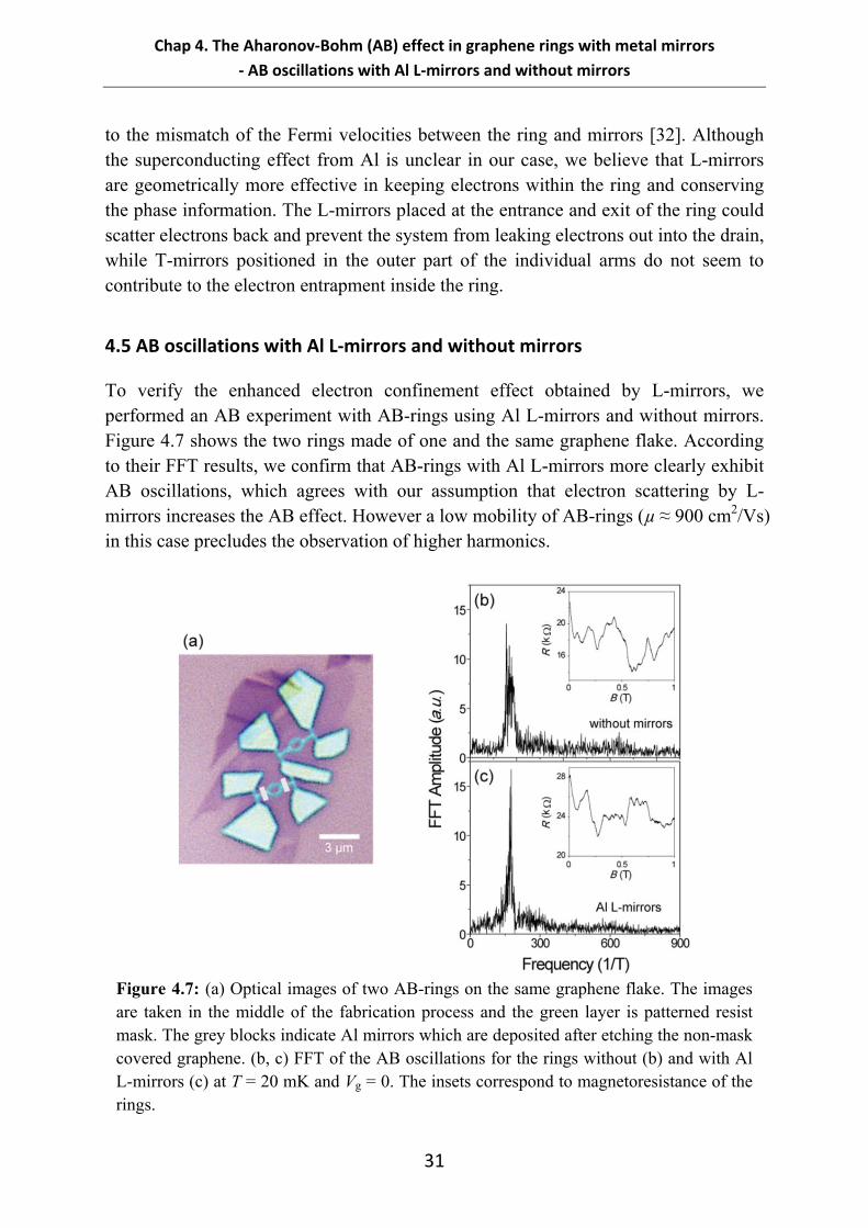
4.5 AB oscillations with Al L‐mirrors and without mirrors
To verify the enhanced electron confinement effect obtained by L-mirrors, we performed an AB experiment with AB-rings using Al L-mirrors and without mirrors. Figure 4.7 shows the two rings made of one and the same graphene flake. According to their FFT results, we confirm that AB-rings with Al L-mirrors more clearly exhibit AB oscillations, which agrees with our assumption that electron scattering by L-mirrors increases the AB effect. However a low mobility of AB-rings (µ ≈ 900 cm2/Vs) in this case precludes the observation of higher harmonics.
Figure 4.7: (a) Optical images of two AB-rings on the same graphene flake. The images are taken in the middle of the fabrication process and the green layer is patterned resist mask. The grey blocks indicate Al mirrors which are deposited after etching the non-mask covered graphene. (b, c) FFT of the AB oscillations for the rings without (b) and with Al L-mirrors (c) at T = 20 mK and Vg = 0. The insets correspond to magnetoresistance of the rings.
Chap 4. The Aharonov‐Bohm (AB) effect in graphene rings with metal mirrors
‐ AB oscillations with Au T‐ mirrors, Au L‐mirrors and without mirrors
32
4.6 AB oscillations with Au T‐ mirrors, Au L‐mirrors and without mirrors
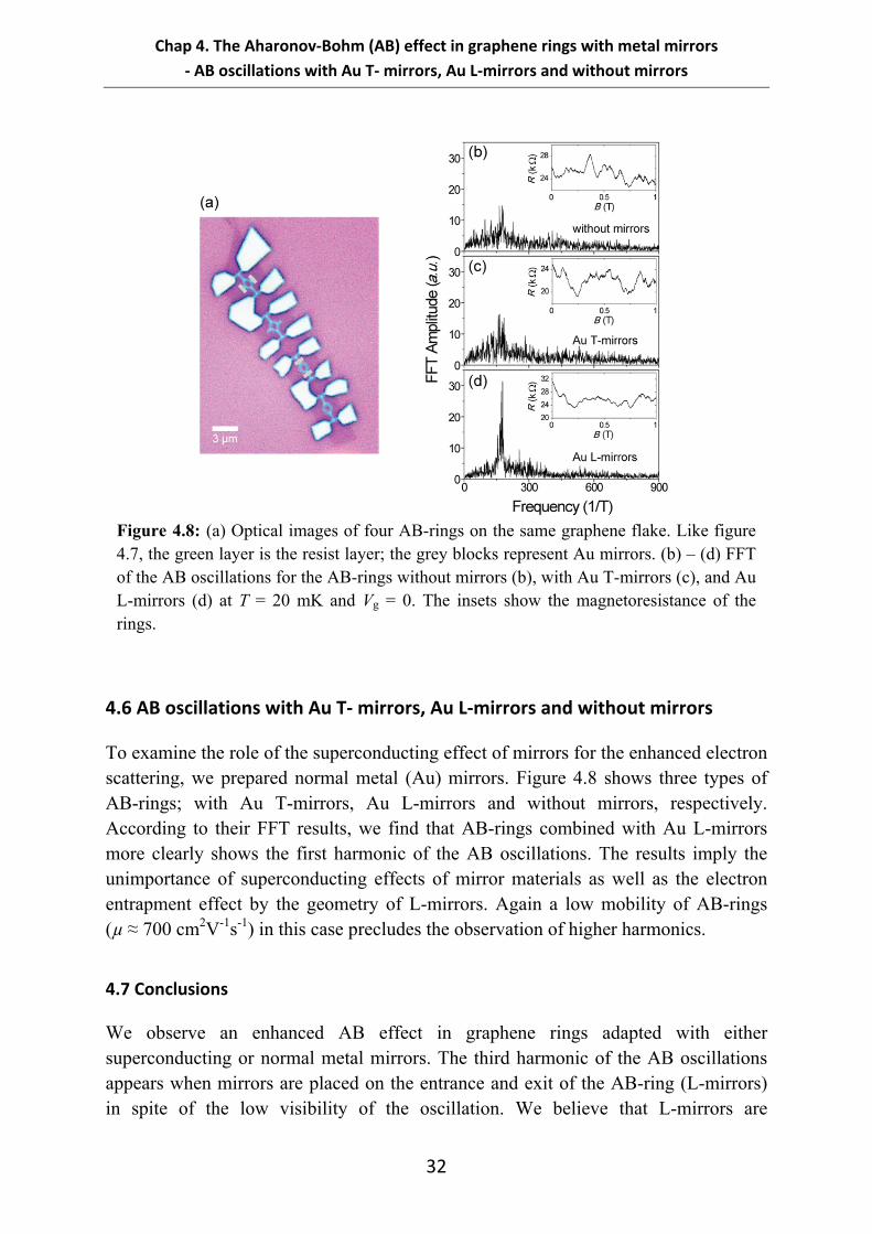
To examine the role of the superconducting effect of mirrors for the enhanced electron scattering, we prepared normal metal (Au) mirrors. Figure 4.8 shows three types of AB-rings; with Au T-mirrors, Au L-mirrors and without mirrors, respectively. According to their FFT results, we find that AB-rings combined with Au L-mirrors more clearly shows the first harmonic of the AB oscillations. The results imply the unimportance of superconducting effects of mirror materials as well as the electron entrapment effect by the geometry of L-mirrors. Again a low mobility of AB-rings (µ ≈ 700 cm2V-1s-1) in this case precludes the observation of higher harmonics.
4.7 Conclusions
We observe an enhanced AB effect in graphene rings adapted with either superconducting or normal metal mirrors. The third harmonic of the AB oscillations appears when mirrors are placed on the entrance and exit of the AB-ring (L-mirrors) in spite of the low visibility of the oscillation. We believe that L-mirrors are
Figure 4.8: (a) Optical images of four AB-rings on the same graphene flake. Like figure 4.7, the green layer is the resist layer; the grey blocks represent Au mirrors. (b) – (d) FFT of the AB oscillations for the AB-rings without mirrors (b), with Au T-mirrors (c), and Au L-mirrors (d) at T = 20 mK and Vg = 0. The insets show the magnetoresistance of the rings.
Chap 4. The Aharonov‐Bohm (AB) effect in graphene rings with metal mirrors
‐ Conclusions
33
geometrically more favourable for keeping electrons within the ring and conserving the phase information. The enhanced electron scattering is attributed to the Fermi velocity mismatch between graphene and mirrors rather than a superconducting effect of the mirrors.

Chap 4. The Aharonov‐Bohm (AB) effect in graphene rings with metal mirrors
‐ Conclusions
34
Chap 5. Unusual thermopower (TEP) of inhomogeneous graphene grown by CVD
‐ Introduction
35
Chapter 5
5. Unusual thermopower (TEP) of inhomogeneous graphene
grown by chemical vapour deposition
5.1 Introduction
Thermopower (TEP) is useful to probe the intrinsic conduction mechanism in graphene together with resistivity measurements. TEP (also known as the Seebeck coefficient S) represents the formation of the electric field E retarding diffusion of charge carriers in response to the temperature gradient T in the open-circuit condition, E = S T. As the direction of the electric field depends on the type of carrier, the sign of TEP can show the type of majority carriers, i.e. S > 0 for holes and S < 0 for electrons.
TEP of the single-layer graphene has been extensively studied both theoretically [39-41] and experimentally [42-46]. In experiments, high quality graphene obtained by mechanical exfoliation from graphite are used in most cases, to reduce the influence of defects and impurities that mask the fundamental thermoelectric transport mechanism. The reported TEP has electron-hole symmetry and its magnitude is usually in the range of ≤ 100 µV/K. The result is usually analyzed by matching it with TEP calculated from electrical conductance data using the semi-classical Mott relation
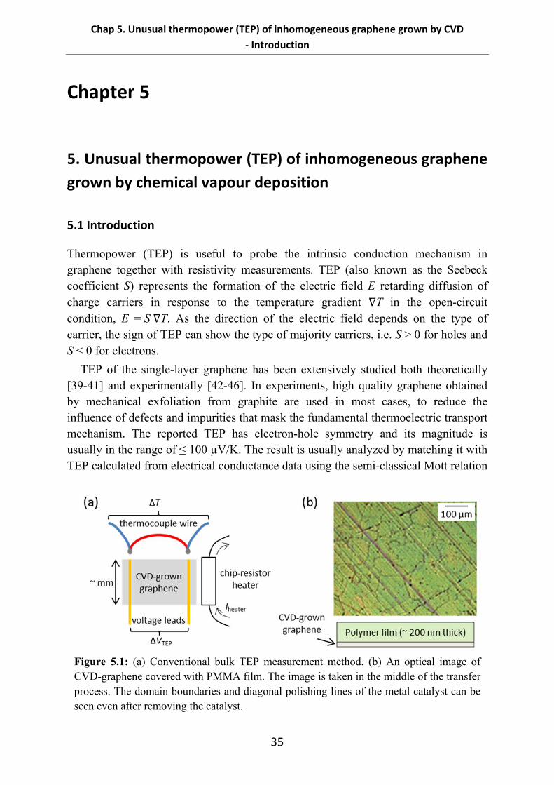
Figure 5.1: (a) Conventional bulk TEP measurement method. (b) An optical image of CVD-graphene covered with PMMA film. The image is taken in the middle of the transfer process. The domain boundaries and diagonal polishing lines of the metal catalyst can be seen even after removing the catalyst.
Chap 5. Unusual thermopower (TEP) of inhomogeneous graphene grown by CVD
‐ The TEP device and experimental details
36
[42, 43, 45].
Meanwhile, the TEP studies on graphene grown by chemical vapour deposition (CVD) have been broadly concerned with application aspects such as gas-flow sensors [47], surface charge doping indicators [48], and energy harvesting devices [49]. Owing to the advantage of producing large-area graphene in the CVD-method, the TEP measurements were performed with a conventional bulk TEP technique by means of wire thermocouples and chip-resistor heaters (figure 5.1(a)). TEP values of millimetre sized CVD-graphene on insulating substrates are directly measured without selecting a clean area, controlling charge carrier density, or applying the magnetic field.
However, the large-area CVD-graphene generally possesses many microscopic defects such as wrinkles and domain boundaries caused during growth and the transfer process, which are overlooked in the previous TEP measurements. Figure 5.1(b) shows the CVD-graphene supported by PMMA. We can notice that the domain boundaries and polishing lines of the metal catalyst remained even after removing the catalyst. To elucidate the influence of inhomogeneity and structural defects on TEP of CVD-graphene, it is essential to measure TEP in micro scale, which is analogous to the previous TEP measurements on the exfoliated graphene.
Here, we report on TEP of inhomogeneous CVD-graphene with respect to the charge carrier density (n), temperature (T), and magnetic field (B). Interestingly, we find a significant electron-hole asymmetry in the TEP while resistance is symmetric. This behaviour can be ascribed to the inhomogeneity of the graphene where individual graphene regions contribute different TEP’s. In high magnetic field and low temperature, we observe anomalously large fluctuations in Sxx near the Dirac point as well as the insulating ν = 0 quantum Hall state, which probably arise from the disorder-induced energy gap opening.
5.2 The TEP device and experimental details
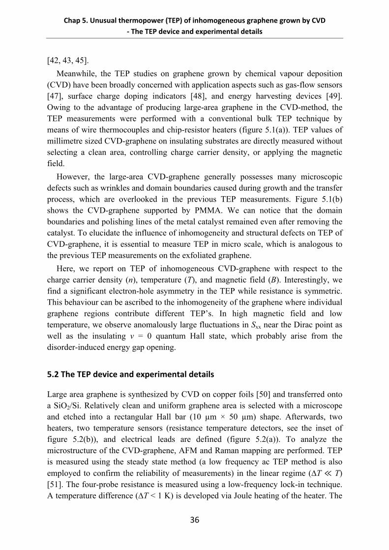
Large area graphene is synthesized by CVD on copper foils [50] and transferred onto a SiO2/Si. Relatively clean and uniform graphene area is selected with a microscope and etched into a rectangular Hall bar (10 µm × 50 µm) shape. Afterwards, two heaters, two temperature sensors (resistance temperature detectors, see the inset of figure 5.2(b)), and electrical leads are defined (figure 5.2(a)). To analyze the microstructure of the CVD-graphene, AFM and Raman mapping are performed. TEP is measured using the steady state method (a low frequency ac TEP method is also employed to confirm the reliability of measurements) in the linear regime (∆T ≪ T) [51]. The four-probe resistance is measured using a low-frequency lock-in technique. A temperature difference (∆T < 1 K) is developed via Joule heating of the heater. The
Chap 5. Unusual thermopower (TEP) of inhomogeneous graphene grown by CVD
‐ AFM and Raman mapping
37
quadratic response of temperature difference and thermoelectric voltage with respect to heater current is shown in figure 5.2(b).
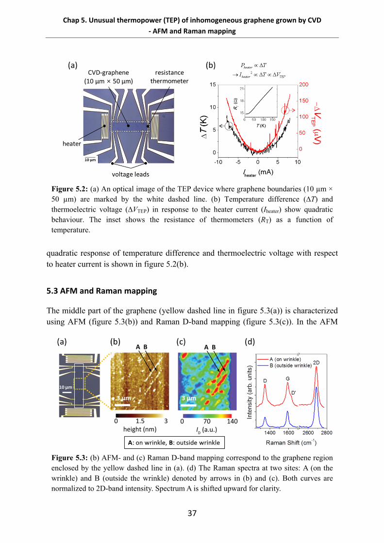
5.3 AFM and Raman mapping
The middle part of the graphene (yellow dashed line in figure 5.3(a)) is characterized using AFM (figure 5.3(b)) and Raman D-band mapping (figure 5.3(c)). In the AFM
Figure 5.3: (b) AFM- and (c) Raman D-band mapping correspond to the graphene region enclosed by the yellow dashed line in (a). (d) The Raman spectra at two sites: A (on the wrinkle) and B (outside the wrinkle) denoted by arrows in (b) and (c). Both curves are normalized to 2D-band intensity. Spectrum A is shifted upward for clarity.
Figure 5.2: (a) An optical image of the TEP device where graphene boundaries (10 µm × 50 µm) are marked by the white dashed line. (b) Temperature difference (∆T) and thermoelectric voltage (∆VTEP) in response to the heater current (Iheater) show quadratic behaviour. The inset shows the resistance of thermometers (RT) as a function of temperature.
Chap 5. Unusual thermopower (TEP) of inhomogeneous graphene grown by CVD
‐ Gate voltage dependence of resistance and TEP
38
scanning image, wrinkles are seen in the diagonal direction. Such wrinkles are common for CVD-graphene, which appears during the growth and transfer process. A similar pattern can be found in the Raman D-band mapping which indicates defect sites and grain boundaries of the graphene [52]. Figure 5.3(d) shows two Raman spectra corresponding to two different sites: A (on the wrinkle) and B (outside the wrinkle). In contrast to flat region B, wrinkled region A has both a stronger intensity of the D-band (≈ 1350 cm-1, related to the inter-valley scattering process) and additional weak D’-band (≈ 1620 cm-1, associated with the intra-valley scattering process in graphene [53]). The D’-band usually arises in the highly defective graphene undergoing intentional deterioration of oxidization, hydrogenation, and fluorination [54, 55]. Therefore, the wrinkled graphene is more disordered than the flat region.
5.4 Gate voltage dependence of resistance and TEP
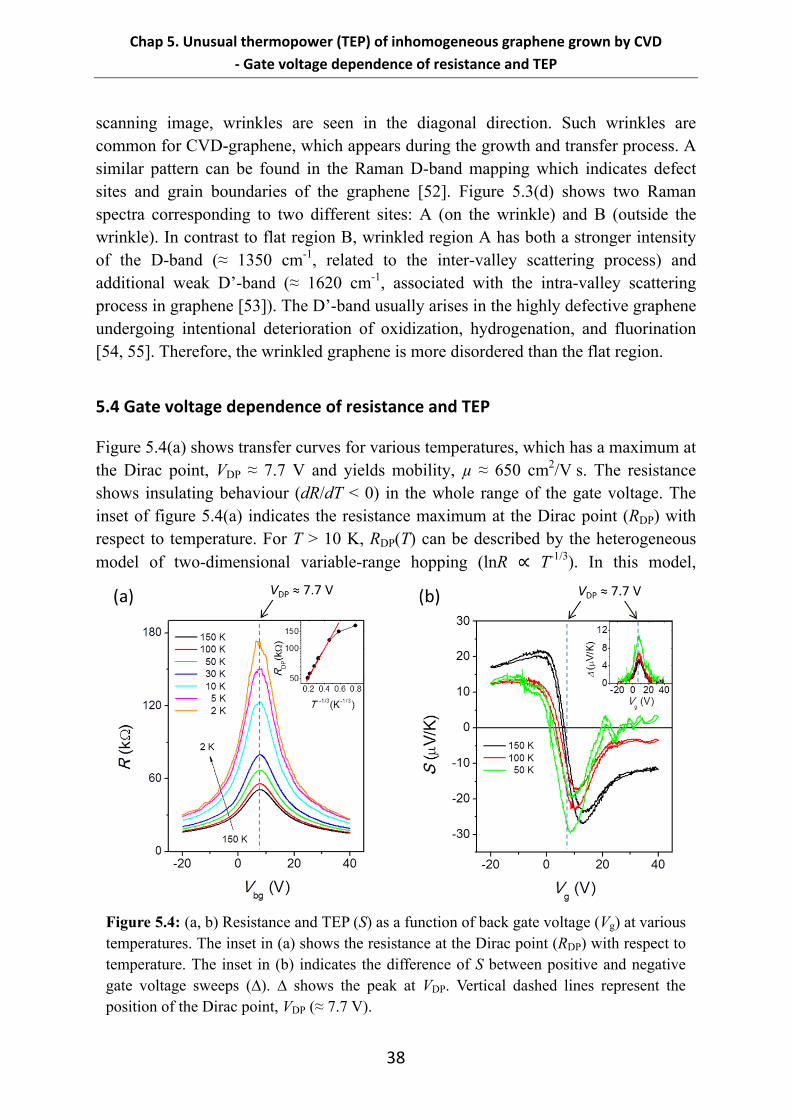
Figure 5.4(a) shows transfer curves for various temperatures, which has a maximum at the Dirac point, VDP ≈ 7.7 V and yields mobility, µ ≈ 650 cm2/V s. The resistance shows insulating behaviour (dR/dT < 0) in the whole range of the gate voltage. The inset of figure 5.4(a) indicates the resistance maximum at the Dirac point (RDP) with respect to temperature. For T > 10 K, RDP(T) can be described by the heterogeneous model of two-dimensional variable-range hopping (lnR ∝ T-1/3). In this model,
Figure 5.4: (a, b) Resistance and TEP (S) as a function of back gate voltage (Vg) at various temperatures. The inset in (a) shows the resistance at the Dirac point (RDP) with respect to temperature. The inset in (b) indicates the difference of S between positive and negative gate voltage sweeps (∆). ∆ shows the peak at VDP. Vertical dashed lines represent the position of the Dirac point, VDP (≈ 7.7 V).
Chap 5. Unusual thermopower (TEP) of inhomogeneous graphene grown by CVD
‐ Gate voltage dependence of resistance and TEP
39
electron conduction is explained with tunnelling between the conducting regions (ordered graphene) [56] which are separated by thin insulating regions (disordered graphene). It agrees with the AFM and Raman mapping results in figure 5.3, which reveal microscopic-scale inhomogeneity in our sample.
Susequently, we measure TEP (S) at various temperatures (figure 5.4(b)). Although TEP of graphene should be an odd function of the gate voltage with respect to the VDP, TEP becomes asymmetrically distorted with decreasing temperature. The zero crossing point of TEP does not match with VDP and shifts to negative voltage. At low temperature (T = 50 K) and Vg > 20 V, TEP even shows positive sign with fluctuations. However, we note that the Dirac point mismatch is not seen for the high mobility CVD-graphene (µ ≈ 3000 cm2/Vs), which is consistent with the TEP of exfoliated graphene [42-44].
The irregular spatial distribution of the electron-hole puddles and inherent inhomogeneity of CVD-graphene would cause the total TEP to have an intricate dependence on the gate voltage and temperature. For instance, if the sample consists of different types of graphene regions in series, the total effective TEP would be given by
( )( )
i g ii
eff gi
i
S V TS V
T
(5.1)
Here Si and ∆Ti are the TEP and the temperature difference in each graphene region, respectively. According to this equation, we can find that the odd-function nature of the generic S(Vg) can be easily distorted if some of the regions are intact to the gate voltage (Sj(Vg) = const). On the contrary, the total resistance R(Vg) in this case would
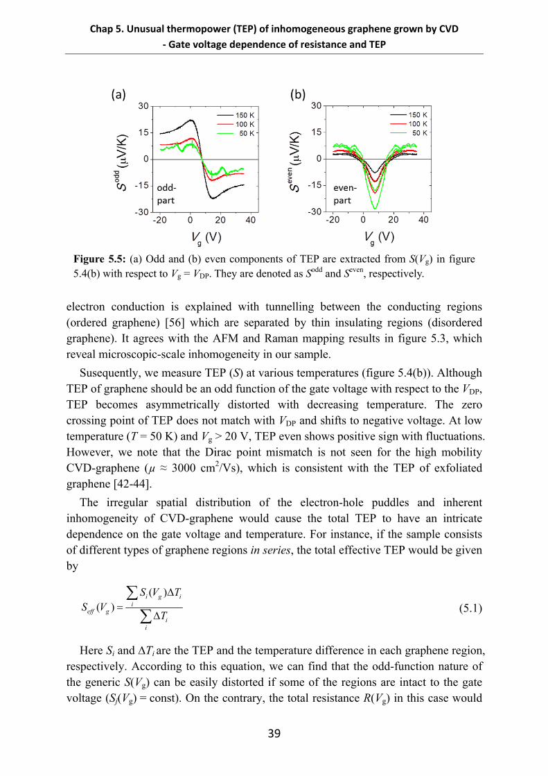
Figure 5.5: (a) Odd and (b) even components of TEP are extracted from S(Vg) in figure 5.4(b) with respect to Vg = VDP. They are denoted as Sodd and Seven, respectively.
Chap 5. Unusual thermopower (TEP) of inhomogeneous graphene grown by CVD
‐ Simulation of inhomogeneity effect using simple mesh
40
just acquire an offset while keeping the symmetry relative to Vg = VDP. Therefore, we believe that the TEP is more sensitive to spatial inhomogeneity of graphene than its resistance.
As seen in figure 5.4(b), S(Vg) shows a hysteresis. Interesingly, the difference of TEP between positive and negative gate sweep directions (defined as ∆ in the inset of the figure 5.4(b)) results in the even function having a peak precisely at VDP. We assume that it somehow reflects the influence of the Dirac point.
Furthermore, S(Vg) are seperated into the odd and even components with respect to Vg = VDP in figure 5.5. We find that the odd component (Sodd) has no hysteresis while the even component (Seven) shows hysteresis and a strong negative dip.
5.5 Simulation of inhomogeneity effect using simple mesh
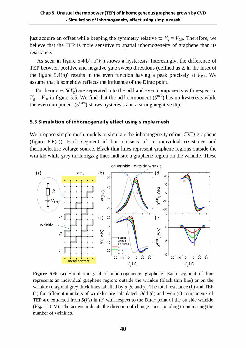
We propose simple mesh models to simulate the inhomogeneity of our CVD-graphene (figure 5.6(a)). Each segment of line consists of an individual resistance and thermoelectric voltage source. Black thin lines represent graphene regions outside the wrinkle while grey thick zigzag lines indicate a graphene region on the wrinkle. These
Figure 5.6: (a) Simulation grid of inhomogeneous graphene. Each segment of line represents an individual graphene region: outside the wrinkle (black thin line) or on the wrinkle (diagonal grey thick lines labelled by α, β, and γ). The total resistance (b) and TEP (c) for different numbers of wrinkles are calculated. Odd (d) and even (e) components of TEP are extracted from S(Vg) in (c) with respect to the Dirac point of the outside wrinkle (VDP = 10 V). The arrows indicate the direction of change corresponding to increasing the number of wrinkles.
Chap 5. Unusual thermopower (TEP) of inhomogeneous graphene grown by CVD
‐ Quantum Hall effect (QHE)
41
two regions are assumed to have a Dirac point at 10- and 0 V, respectively.
By solving Kirchhoff’s equations in this network, we calculate the variation of the total resistance R(Vg) and TEP, S(Vg) when changing the number of wrinkles in figure 5.6(b) and (c), respectively. As a result, S(Vg) becomes more distorted and asymmetric compared to R(Vg) with an increasing number of wrinkles. The even and odd components are extracted in figure 5.6(d) and (e), respectively. This simplified model allows us to qualitatively understand the sensitivity of TEP to sample inhomogeneity [57].
5.6 Quantum Hall effect (QHE)
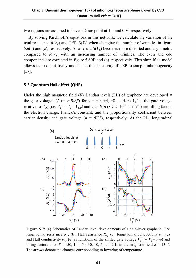
Under the high magnetic field (B), Landau levels (LL) of graphene are developed at the gate voltage Vg’ (= νeB/hβ) for ν = ±0, ±4, ±8…. Here Vg’ is the gate voltage relative to VDP (i.e. Vg’ = Vg – VDP) and ν, e, h, β (∼7.2×1010 cm-2V-1) are filling factors, the electron charge, Planck’s constant, and the proportionality coefficient between carrier density and gate voltage (n = βVg’), respectively. At the LL, longitudinal
Figure 5.7: (a) Schematics of Landau level developments of single-layer graphene. The longitudinal resistance Rxx (b), Hall resistance Rxy (c), longitudinal conductivity σxx (d) and Hall conductivity σxy (e) as functions of the shifted gate voltage Vg’ (= Vg – VDP) and filling factors ν for T = 150, 100, 50, 30, 10, 5, and 2 K in the magnetic field B = 13 T. The arrows denote the changes corresponding to lowering of temperature.
Chap 5. Unusual thermopower (TEP) of inhomogeneous graphene grown by CVD
‐ Magneto TEP
42
conductivity σxx(Vg’) shows the peak while Hall conductiviy σxy(Vg’) changes abruptly. Between the LLs, σxx(Vg’) becomes zero while σxy(Vg’) shows the half-integer quantum Hall plateaus, σxy = -νe2/h with ν = ±2, ±6, ±10….. Here, the integer step of 4 in ν is due to the four-fold degeneracy of graphene LL from spin- and valley degeneracy.
Figure 5.7 shows the quantum Hall effect of CVD-graphene in the magnetic field of 13 T. Based on the measurements of longitudinal resistance (Rxx) and Hall resistance (Rxy,), we calculate σxx and σxy. Interestingly, at ν = 0, σxx (σxy) shows an unexpected dip (plateau) and this becomes pronounced with decreasing temperature. We believe that it is due to a gap formation near the Dirac point (at ν = 0) resulting in slight splitting of the central LL (N = 0).
So far, the insulating ν = 0 quantum Hall state has been experimentally observed in high quality samples made of exfoliated graphene [58-62]. The behaviours are usually attributed to lifting of LL (spin-valley symmetry breaking) [58, 62], counter-propagating edge states [59], and magnetic field induced gap opening [60, 61]. Howerever, we suppose that in our case the behaviour is due to the disorder induced gap opening at the Dirac point [49, 63-66].
5.7 Magneto TEP
Under the high magnetic field, longitudinal TEP (Sxx) can be described as in eq. 5.2.
2 2
xx xx xy xyxx
xx xy
S
where
1( ) '( )ij F ij
fd
eT
(5.2)
Here, σij’ is energy-dependent partial conductivity (i.e., / '( )ij ijf d )
(the TEP formula without magnetic field is explained in chapter 2.2)
Accordingly, Sxx of graphene has peaks near LL (|N| ≥ 1) and is zero between the LLs. In particular, at the Dirac point, Sxx is zero with two accompanying peaks of opposite sign owing to the nature of the central LL (N = 0, zeroth LL) where both electrons and holes coexist [41-44].
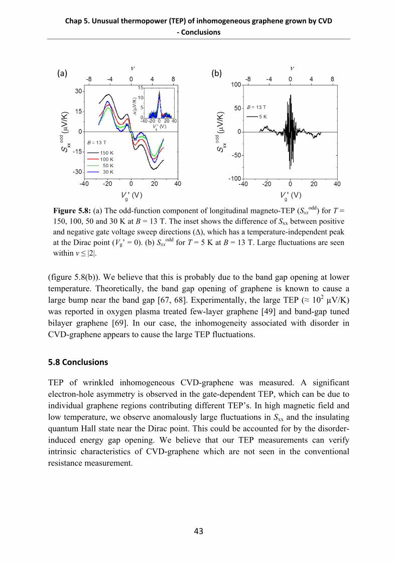
Figure 5.8(a) shows the odd-function component of Sxx (denoted as Sxxodd) at
various temperatures. The overall magnitude of Sxxodd decreases with lowering
temperature except for the peaks T = 30 K which start to increase. Here the two peaks at ν = |4| are attributed to the LL (|N| = 1) development of graphene. The inset displays the sweep-direction difference of Sxx. We find that ∆ has temperature-independent peaks near the Dirac point similar to TEP without magnetic field (inset in figure 5.4(b)).
Interesitingly, at T = 5 K, Sxxodd shows large fluctuations near the central LL (N = 0)
Chap 5. Unusual thermopower (TEP) of inhomogeneous graphene grown by CVD
‐ Conclusions
43
(figure 5.8(b)). We believe that this is probably due to the band gap opening at lower temperature. Theoretically, the band gap opening of graphene is known to cause a large bump near the band gap [67, 68]. Experimentally, the large TEP (≈ 102 µV/K) was reported in oxygen plasma treated few-layer graphene [49] and band-gap tuned bilayer graphene [69]. In our case, the inhomogeneity associated with disorder in CVD-graphene appears to cause the large TEP fluctuations.
5.8 Conclusions
TEP of wrinkled inhomogeneous CVD-graphene was measured. A significant electron-hole asymmetry is observed in the gate-dependent TEP, which can be due to individual graphene regions contributing different TEP’s. In high magnetic field and low temperature, we observe anomalously large fluctuations in Sxx and the insulating quantum Hall state near the Dirac point. This could be accounted for by the disorder-induced energy gap opening. We believe that our TEP measurements can verify intrinsic characteristics of CVD-graphene which are not seen in the conventional resistance measurement.
Figure 5.8: (a) The odd-function component of longitudinal magneto-TEP (Sxx
odd) for T = 150, 100, 50 and 30 K at B = 13 T. The inset shows the difference of Sxx between positive and negative gate voltage sweep directions (∆), which has a temperature-independent peak at the Dirac point (Vg’ = 0). (b) Sxx
odd for T = 5 K at B = 13 T. Large fluctuations are seen within ν ≤ |2|.
Chap 5. Unusual thermopower (TEP) of inhomogeneous graphene grown by CVD
‐ Conclusions
44
Chap 6. Graphene p‐n‐p junctions made of naturally oxidized thin aluminium films
‐ Introduction
45
Chapter 6
6. Graphene p‐n‐p junctions made of naturally oxidized thin
aluminium films
6.1 Introduction
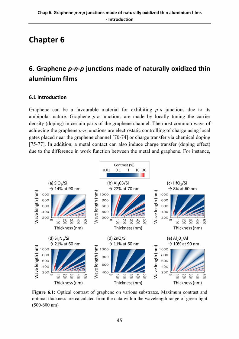
Graphene can be a favourable material for exhibiting p-n junctions due to its ambipolar nature. Graphene p-n junctions are made by locally tuning the carrier density (doping) in certain parts of the graphene channel. The most common ways of achieving the graphene p-n junctions are electrostatic controlling of charge using local gates placed near the graphene channel [70-74] or charge transfer via chemical doping [75-77]. In addition, a metal contact can also induce charge transfer (doping effect) due to the difference in work function between the metal and graphene. For instance,
Figure 6.1: Optical contrast of graphene on various substrates. Maximum contrast and optimal thickness are calculated from the data within the wavelength range of green light (500-600 nm)
Chap 6. Graphene p‐n‐p junctions made of naturally oxidized thin aluminium films
‐ The graphene p‐n‐p device and experimental details
46
aluminium (Al) in contact with graphene can cause n-type doping [14-17] mainly because the work function of Al (WAl) is lower than that of graphene (Wgraphene) (i.e., Wmetal-Wgraphene = -0.44 ~ -0.24).
Here, we employ a narrow Al strip on the middle part of the graphene channel. The Al plays the role of both a local top-gate and a charge donor. The Al is directly deposited on graphene without a prior dielectric layer in between. In the air, the Al at the interface of graphene becomes oxidized and this can be used for a dielectric layer. When the Al top-gate is floating and aluminium oxide (Al2O3) is used for the back-gate dielectric (instead of the commonly used 300 nm thick SiO2), we observe a significant double-peak behaviour with a hysteresis in the transfer curves (source-drain resistance R versus back-gate voltage Vbg). The double-peak feature can be a proof of the formation of graphene p-n junctions. The hysteresis can be explained by assuming finite resistance of the aluminium oxide at the interface of Al and graphene and considering the capacitive coupling between the gates.
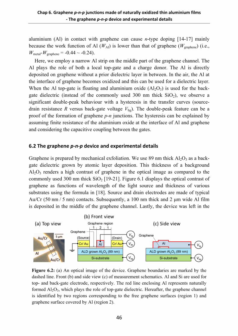
6.2 The graphene p‐n‐p device and experimental details
Graphene is prepared by mechanical exfoliation. We use 89 nm thick Al2O3 as a back-gate dielectric grown by atomic layer deposition. This thickness of a background Al2O3 renders a high contrast of graphene in the optical image as compared to the commonly used 300 nm thick SiO2 [19-21]. Figure 6.1 displays the optical contrast of graphene as functions of wavelength of the light source and thickness of various substrates using the formula in [18]. Source and drain electrodes are made of typical Au/Cr (50 nm / 5 nm) contacts. Subsequently, a 100 nm thick and 2 μm wide Al film is deposited in the middle of the graphene channel. Lastly, the device was left in the
Figure 6.2: (a) An optical image of the device. Graphene boundaries are marked by the dashed line. Front (b) and side view (c) of measurement schematics. Al and Si are used for top- and back-gate electrode, respectively. The red line enclosing Al represents naturally formed Al2O3, which plays the role of top-gate dielectric. Hereafter, the graphene channel is identified by two regions corresponding to the free graphene surfaces (region 1) and graphene surface covered by Al (region 2).
Chap 6. Graphene p‐n‐p junctions made of naturally oxidized thin aluminium films
‐ Al oxidation at the interface with graphene
47
air for several days to fully oxidize the Al at the interface to the graphene [17, 78]. The naturally formed Al2O3 is utilized as a top-gate dielectric layer. An optical image and measurement schematics are shown in figure 6.2. All the measurements were carried out at room temperature. Dual-gate experiments (in chapters 6.4 and 6.5) were performed in nitrogen atmosphere to stabilize Al oxidization.
6.3 Al oxidation at the interface with graphene
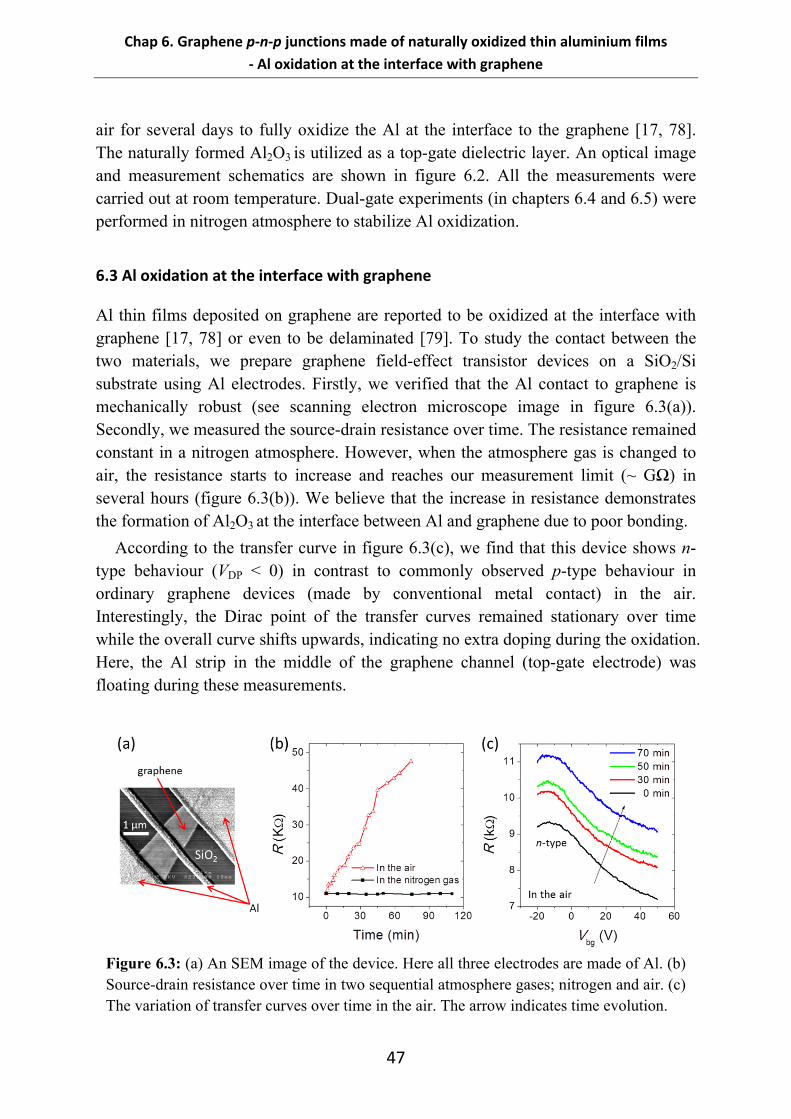
Al thin films deposited on graphene are reported to be oxidized at the interface with graphene [17, 78] or even to be delaminated [79]. To study the contact between the two materials, we prepare graphene field-effect transistor devices on a SiO2/Si substrate using Al electrodes. Firstly, we verified that the Al contact to graphene is mechanically robust (see scanning electron microscope image in figure 6.3(a)). Secondly, we measured the source-drain resistance over time. The resistance remained constant in a nitrogen atmosphere. However, when the atmosphere gas is changed to air, the resistance starts to increase and reaches our measurement limit (~ GΩ) in several hours (figure 6.3(b)). We believe that the increase in resistance demonstrates the formation of Al2O3 at the interface between Al and graphene due to poor bonding.
According to the transfer curve in figure 6.3(c), we find that this device shows n-type behaviour (VDP < 0) in contrast to commonly observed p-type behaviour in ordinary graphene devices (made by conventional metal contact) in the air. Interestingly, the Dirac point of the transfer curves remained stationary over time while the overall curve shifts upwards, indicating no extra doping during the oxidation. Here, the Al strip in the middle of the graphene channel (top-gate electrode) was floating during these measurements.
Figure 6.3: (a) An SEM image of the device. Here all three electrodes are made of Al. (b) Source-drain resistance over time in two sequential atmosphere gases; nitrogen and air. (c) The variation of transfer curves over time in the air. The arrow indicates time evolution.
Chap 6. Graphene p‐n‐p junctions made of naturally oxidized thin aluminium films
‐ Dual‐gate effect using the aluminium top gate
48
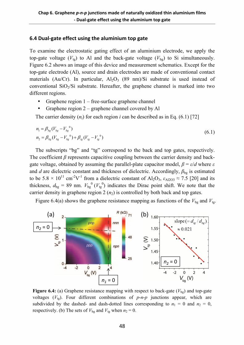
6.4 Dual‐gate effect using the aluminium top gate
To examine the electrostatic gating effect of an aluminium electrode, we apply the top-gate voltage (Vtg) to Al and the back-gate voltage (Vbg) to Si simultaneously. Figure 6.2 shows an image of this device and measurement schematics. Except for the top-gate electrode (Al), source and drain electrodes are made of conventional contact materials (Au/Cr). In particular, Al2O3 (89 nm)/Si substrate is used instead of conventional SiO2/Si substrate. Hereafter, the graphene channel is marked into two different regions.
Graphene region 1 – free-surface graphene channel Graphene region 2 – graphene channel covered by Al
The carrier density (ni) for each region i can be described as in Eq. (6.1) [72]
01
0 02
( )
( ) ( )
bg bg bg
bg bg bg tg tg tg
n V V
n V V V V
(6.1)
The subscripts “bg” and “tg” correspond to the back and top gates, respectively. The coefficient β represents capacitive coupling between the carrier density and back-gate voltage, obtained by assuming the parallel-plate capacitor model, β = ε/d where ε and d are dielectric constant and thickness of dielectric. Accordingly, βbg is estimated to be 5.8 × 1011 cm-2V-1 from a dielectric constant of Al2O3, εAl2O3 ≈ 7.5 [20] and its thickness, dbg = 89 nm. Vbg
0 (Vtg0) indicates the Dirac point shift. We note that the
carrier density in graphene region 2 (n2) is controlled by both back and top gates.
Figure 6.4(a) shows the graphene resistance mapping as functions of the Vbg and Vtg.
Figure 6.4: (a) Graphene resistance mapping with respect to back-gate (Vbg) and top-gate voltages (Vtg). Four different combinations of p-n-p junctions appear, which are subdivided by the dashed- and dash-dotted lines corresponding to n1 = 0 and n2 = 0, respectively. (b) The sets of Vbg and Vtg when n2 = 0.
Chap 6. Graphene p‐n‐p junctions made of naturally oxidized thin aluminium films
‐ Double‐peak structure in the transfer curve when Al top gate is floating
49
We can see four different combinations of p-n-p junctions subdivided by two resistance ridges (dashed lines) corresponding to n1 = 0 and n2 = 0, respectively. According to the slope of the ridge for n2 = 0 (βbg/βtg = dtg/dbg ∼ 0.021, see figure 6.4(b)), the thickness of the top-gate Al2O3 (dbg) can be derived to be ≈ 2 nm. Here we assume the same dielectric constant for the back- and top-gate dielectric Al2O3.
6.5 Double‐peak structure in the transfer curve when Al top gate is floating
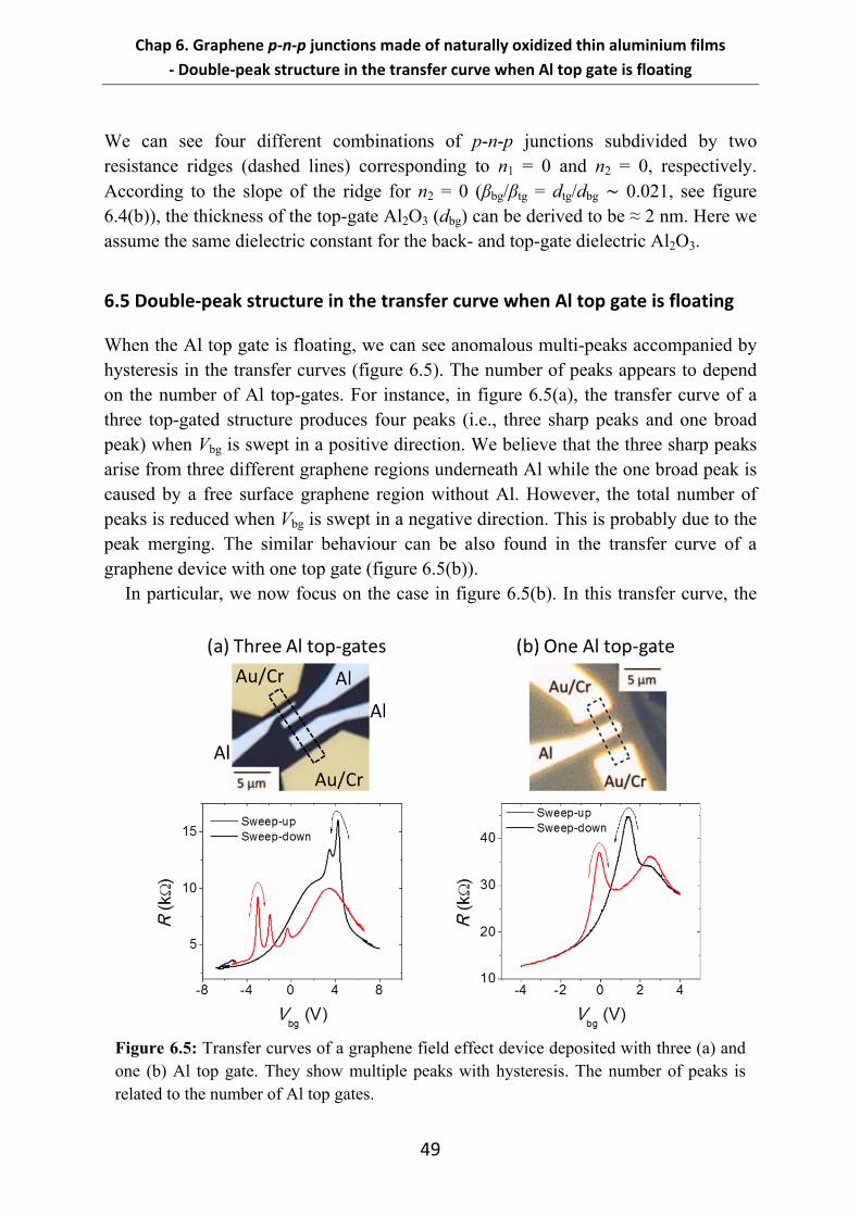
When the Al top gate is floating, we can see anomalous multi-peaks accompanied by hysteresis in the transfer curves (figure 6.5). The number of peaks appears to depend on the number of Al top-gates. For instance, in figure 6.5(a), the transfer curve of a three top-gated structure produces four peaks (i.e., three sharp peaks and one broad peak) when Vbg is swept in a positive direction. We believe that the three sharp peaks arise from three different graphene regions underneath Al while the one broad peak is caused by a free surface graphene region without Al. However, the total number of peaks is reduced when Vbg is swept in a negative direction. This is probably due to the peak merging. The similar behaviour can be also found in the transfer curve of a graphene device with one top gate (figure 6.5(b)).
In particular, we now focus on the case in figure 6.5(b). In this transfer curve, the
Figure 6.5: Transfer curves of a graphene field effect device deposited with three (a) and one (b) Al top gate. They show multiple peaks with hysteresis. The number of peaks is related to the number of Al top gates.
Chap 6. Graphene p‐n‐p junctions made of naturally oxidized thin aluminium films
‐ Double‐peak structure in the transfer curve when Al top gate is floating
50
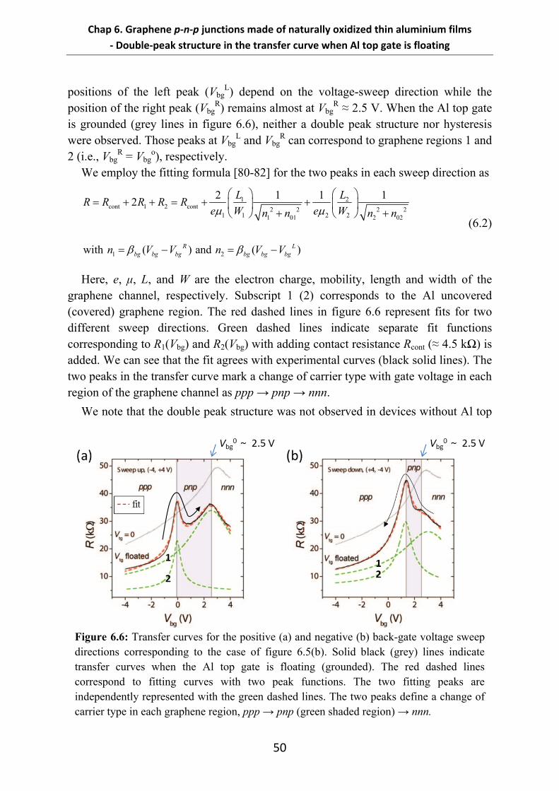
positions of the left peak (VbgL) depend on the voltage-sweep direction while the
position of the right peak (VbgR) remains almost at Vbg
R ≈ 2.5 V. When the Al top gate is grounded (grey lines in figure 6.6), neither a double peak structure nor hysteresis were observed. Those peaks at Vbg
L and VbgR can correspond to graphene regions 1 and
2 (i.e., VbgR = Vbg
o), respectively. We employ the fitting formula [80-82] for the two peaks in each sweep direction as
1 2cont 1 2 cont 2 2 2 2
1 1 2 21 01 2 02
1 2
2 1 1 12
with ( ) and ( )R Lbg bg bg bg bg bg
L LR R R R R
e W e Wn n n n
n V V n V V
(6.2)
Here, e, μ, L, and W are the electron charge, mobility, length and width of the graphene channel, respectively. Subscript 1 (2) corresponds to the Al uncovered (covered) graphene region. The red dashed lines in figure 6.6 represent fits for two different sweep directions. Green dashed lines indicate separate fit functions corresponding to R1(Vbg) and R2(Vbg) with adding contact resistance Rcont (≈ 4.5 kΩ) is added. We can see that the fit agrees with experimental curves (black solid lines). The two peaks in the transfer curve mark a change of carrier type with gate voltage in each region of the graphene channel as ppp → pnp → nnn.
We note that the double peak structure was not observed in devices without Al top
Figure 6.6: Transfer curves for the positive (a) and negative (b) back-gate voltage sweep directions corresponding to the case of figure 6.5(b). Solid black (grey) lines indicate transfer curves when the Al top gate is floating (grounded). The red dashed lines correspond to fitting curves with two peak functions. The two fitting peaks are independently represented with the green dashed lines. The two peaks define a change of carrier type in each graphene region, ppp → pnp (green shaded region) → nnn.
Chap 6. Graphene p‐n‐p junctions made of naturally oxidized thin aluminium films
‐ Circuit model to account for the hysteresis in the double‐peak structure
51
gates and the mobility of the device has reduced from 3100- to 650 cm2V-1s-1 after Al top-gate deposition. The double peak structure weakly depends on the sweep rate and it does not appear when SiO2 is used for the back-gate dielectric instead of Al2O3.
6.6 Circuit model to account for the hysteresis in the double‐peak structure
In order to explain the hysteresis in the double peak structure, we consider a simplified equivalent circuit (figure 6.7(a)) for the graphene region 2. Here, R represents the resistance of the top-gate dielectric (naturally formed Al2O3). C0 is the capacitance between the back- and top-gate electrodes. The calculated capacitances of C0, Ctg, and Cbg from our device geometry are about 240 pF, 82.6 fF, and 1.86 fF, respectively.
From the circuit model, the induced Vtg in response to linearly increasing Vbg with time (Vbg = αt) is given by
0
1 exptg tg
tg
tV RI
R C C
(6.3)
Here, Itg(= C0α ≈ 20 pA) is the current flowing across the top-gate dielectric. Now considering an infinite triangular Vbg of amplitude A and period T, we find that Vtg results in two different functions for opposite sweep directions (hysteresis) given as
Figure 6.7: (a) The equivalent circuit corresponding to the dual-gated graphene region 2. C0 is the capacitance between the back- and top-gate electrodes. Red dashed circle represents top-gate dielectric where R is its resistance. (b) The calculated Vtg in response to the applied Vbg using the circuit shown in (a). The voltage induced on the floating top-gate shows a hysteresis. (c) The calculated carrier density for each graphene region as a function of Vbg.
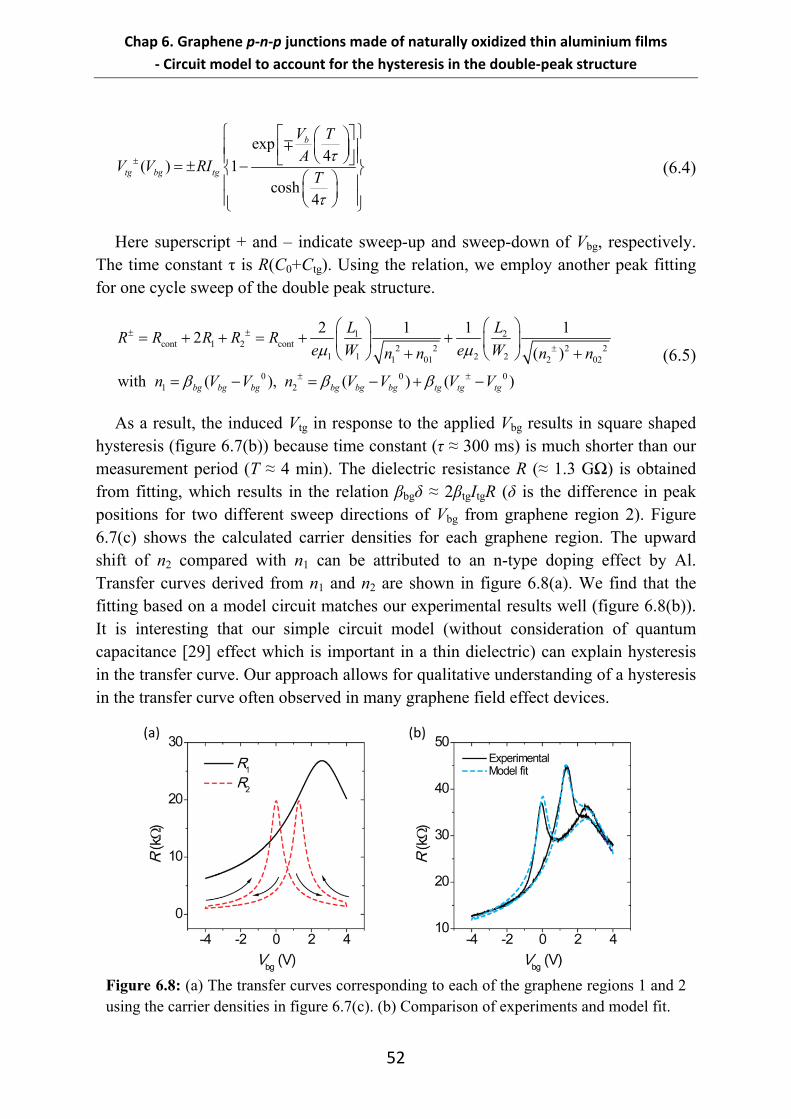
Chap 6. Graphene p‐n‐p junctions made of naturally oxidized thin aluminium films
‐ Circuit model to account for the hysteresis in the double‐peak structure
52
exp4
( ) 1cosh
4
b
tg bg tg
V TA
V V RIT
(6.4)
Here superscript + and – indicate sweep-up and sweep-down of Vbg, respectively. The time constant τ is R(C0+Ctg). Using the relation, we employ another peak fitting for one cycle sweep of the double peak structure.
1 2cont 1 2 cont 2 2 2 2
1 1 2 21 01 2 02
0 0 01 2
2 1 1 12
( )
with ( ), ( ) ( )bg bg bg bg bg bg tg tg tg
L LR R R R R
e W e Wn n n n
n V V n V V V V
(6.5)
As a result, the induced Vtg in response to the applied Vbg results in square shaped hysteresis (figure 6.7(b)) because time constant (τ ≈ 300 ms) is much shorter than our measurement period (T ≈ 4 min). The dielectric resistance R (≈ 1.3 GΩ) is obtained from fitting, which results in the relation βbgδ ≈ 2βtgItgR (δ is the difference in peak positions for two different sweep directions of Vbg from graphene region 2). Figure 6.7(c) shows the calculated carrier densities for each graphene region. The upward shift of n2 compared with n1 can be attributed to an n-type doping effect by Al. Transfer curves derived from n1 and n2 are shown in figure 6.8(a). We find that the fitting based on a model circuit matches our experimental results well (figure 6.8(b)). It is interesting that our simple circuit model (without consideration of quantum capacitance [29] effect which is important in a thin dielectric) can explain hysteresis in the transfer curve. Our approach allows for qualitative understanding of a hysteresis in the transfer curve often observed in many graphene field effect devices.
Figure 6.8: (a) The transfer curves corresponding to each of the graphene regions 1 and 2 using the carrier densities in figure 6.7(c). (b) Comparison of experiments and model fit.
Chap 6. Graphene p‐n‐p junctions made of naturally oxidized thin aluminium films
‐ Conclusions
53
6.7 Conclusions
A naturally formed thin Al2O3 layer at the interface with graphene and Al top-gate is employed for the dielectric layer, which enables us to realise graphene p-n-p junctions. When the top-gate is electrically floating, the graphene resistance in response to the slowly-varying back-gate voltage shows a double peak structure accompanied by a hysteresis. This could indicate the Al-doping effect and capacitive coupling between top- and back gate electrodes.

Chap 6. Graphene p‐n‐p junctions made of naturally oxidized thin aluminium films
‐ Conclusions
54
Chap 7. Quantum Hall effect in graphene decorated with disordered multilayer patches
‐ Introduction
55
Chapter 7
7. Quantum Hall effect in graphene decorated with
disordered multilayer patches
7.1 Introduction
The integer quantum Hall effect (QHE) is a hallmark of a two-dimensional (2D) electron gas formed at the interface between semiconductors or their surfaces [83, 84]. Graphene is a perfect two-dimensional 2D material [1]. Unlike the conventional 2D electron gas, graphene shows a half-integer QHE due to a Berry’s phase π [3, 4]. The half-integer QHE in graphene demonstrates not only 2D nature of graphene but also its unique Dirac-like electronic structure associated with the spin- and valley degeneracy and the feature of the central Landau level (LL) where electrons and holes coexist.
Generally, in order to observe the QHE three essential conditions are usually required: low temperatures (< 4 K), high magnetic fields (≥ 10 T), and clean samples with high mobility (> 103 cm2V-1s-1). This makes LL’s more discrete by decreasing the width of LL’s and increasing the energy spacing between adjacent LL’s. Indeed, most of QHE experiments (including fractional QHE) on graphene were performed under these conditions [3, 4, 58, 60, 85-87]. Exceptionally, graphene QHE was observed even at room-temperature [88] explained by the fact that graphene innately has an unequal energy spacing between LL’s and an anomalously large energy spacing between the central LL and it nearest LL’s, compared to an ordinary 2D electron gas. The ultra-high magnetic field (~ 30 T) and notably high mobility of the sample (> 104 cm2V-1s-1) used in this experiment also helped to see the QHE at room temperature. Meanwhile, the weak QHE associated with relatively low mobility 2D gas system is usually employed to study a magnetic field induced transition from the Anderson localization (insulator) to quantum Hall sate (conductor) [89, 90]. Recently, the transition was also observed in low mobility graphene (≈ 900 cm2V-1s-1) grown on silicon carbide [91].
The width Γ of LL’s and the energy spacing ΔE of between LL’s are determined by the mobility µ and magnetic field B. The high mobility assures the small Γ because of the uncertainty relation Γ·τ ~ ħ, where ħ is Planck’s constant divided by 2π and τ is the momentum relaxation time which is proportional to the mobility. The high magnetic field increases ΔE (= ħwc) since the cyclotron frequency wc is proportional to the
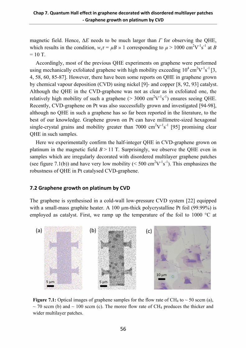
Chap 7. Quantum Hall effect in graphene decorated with disordered multilayer patches
‐ Graphene growth on platinum by CVD
56
magnetic field. Hence, ΔE needs to be much larger than Γ for observing the QHE, which results in the condition, wcτ = µB » 1 corresponding to µ > 1000 cm2V-1s-1 at B = 10 T.
Accordingly, most of the previous QHE experiments on graphene were performed using mechanically exfoliated graphene with high mobility exceeding 104 cm2V-1s-1 [3, 4, 58, 60, 85-87]. However, there have been some reports on QHE in graphene grown by chemical vapour deposition (CVD) using nickel [9]- and copper [8, 92, 93] catalyst. Although the QHE in the CVD-graphene was not as clear as in exfoliated one, the relatively high mobility of such a graphene (> 3000 cm2V-1s-1) ensures seeing QHE. Recently, CVD-graphene on Pt was also successfully grown and investigated [94-98], although no QHE in such a graphene has so far been reported in the literature, to the best of our knowledge. Graphene grown on Pt can have millimetre-sized hexagonal single-crystal grains and mobility greater than 7000 cm2V-1s-1 [95] promising clear QHE in such samples.
Here we experimentally confirm the half-integer QHE in CVD-graphene grown on platinum in the magnetic field B > 11 T. Surprisingly, we observe the QHE even in samples which are irregularly decorated with disordered multilayer graphene patches (see figure 7.1(b)) and have very low mobility (< 500 cm2V-1s-1). This emphasizes the robustness of QHE in Pt catalysed CVD-graphene.
7.2 Graphene growth on platinum by CVD
The graphene is synthesised in a cold-wall low-pressure CVD system [22] equipped with a small-mass graphite heater. A 100 µm-thick polycrystalline Pt foil (99.99%) is employed as catalyst. First, we ramp up the temperature of the foil to 1000 °C at
Figure 7.1: Optical images of graphene samples for the flow rate of CH4 to ~ 50 sccm (a), ~ 70 sccm (b) and ~ 100 sccm (c). The moree flow rate of CH4 produces the thicker and wider multilayer patches.
Chap 7. Quantum Hall effect in graphene decorated with disordered multilayer patches
‐ Transfer curves and Raman mapping
57
300 °C/min and hold it at this temperature for 5 min in a flow of 1000 sccm H2. We note that the growth temperature of 1000 °C is the nominal temperature obtained from a thermocouple sensor gently touching the heater. For instance, the nominal value corresponding to Cu melting point is about 850 °C. Therefore, we believe actual temperature in this case can be 100 – 200 °C higher. Then, 70 sccm CH4 pre-diluted with Ar to 5% is introduced into the chamber to activate graphene growth. The growth time is 10 minutes. Finally, the foil is cooled down to below 100 °C within 15 minutes by turning off the heater current. The CH4 is kept flowing while cooling down. The high melting point (≈ 1770 °C) of Pt enables us to easily and reliably access high temperature over 1000 °C which is impossible to achieve with conventional Cu catalyst. In comparison to previous graphene growth on Pt [95-97] performed under atmospheric pressure and temperature ≈ 1000 °C, we use low-pressure condition with low carbon concentration and temperature > 1000 °C.
We notice that changing the flow rate of CH4 to somewhat in excess of ~ 50 sccm gives rise to additional multilayer graphene patches of ~ 5 µm in size (figure 7.1(b)) whereas the overflow of CH4 (> 100 sccm) generates much thicker and larger multilayer patches (figure 7.1(c)). This means that the thickness and size of the patches are easily controllable by the flow rate of CH4.
Afterwards, the graphene is transferred onto a highly doped Si substrate capped with 300 nm SiO2, allowing for a field-effect transistor structure. We employ the frame-assisted bubbling transfer technique [95, 99] instead of usual wet etching of the metal catalyst thereby avoiding etching residues and possible damage of graphene caused by strong acids as in the case of Pt catalyst. The semi-rigid frame supporting the PMMA coated graphene allows for easy handling and cleaning of graphene [99]. Using the frame, we can rinse graphene more thoroughly during the transfer process. Lastly, graphene Hall bar structures (≈ 10 × 40 µm2) are patterned using a standard micro fabrication process.
7.3 Transfer curves and Raman mapping
Figure 7.2(a) shows an optical image of our graphene sample placed on the SiO2/Si substrate. The image contrast is sufficient to discern the boundary of graphene and its inhomogeneous structure. We can see that relatively dark patches (< 5 µm) are scattered all over the sample. The patchy structure is made by increasing the flow rate of CH4 to about 70 sccm during the growth process compared to the optimal flow rate of CH4 ~ 50 sccm for growing a single-layer graphene without patches (figure 7.1(a)). If we further increased the flow rate of CH4, much thicker pyramid-like patches would be formed where several graphene layers would be clearly distinguishable (figure 7.1(c)).
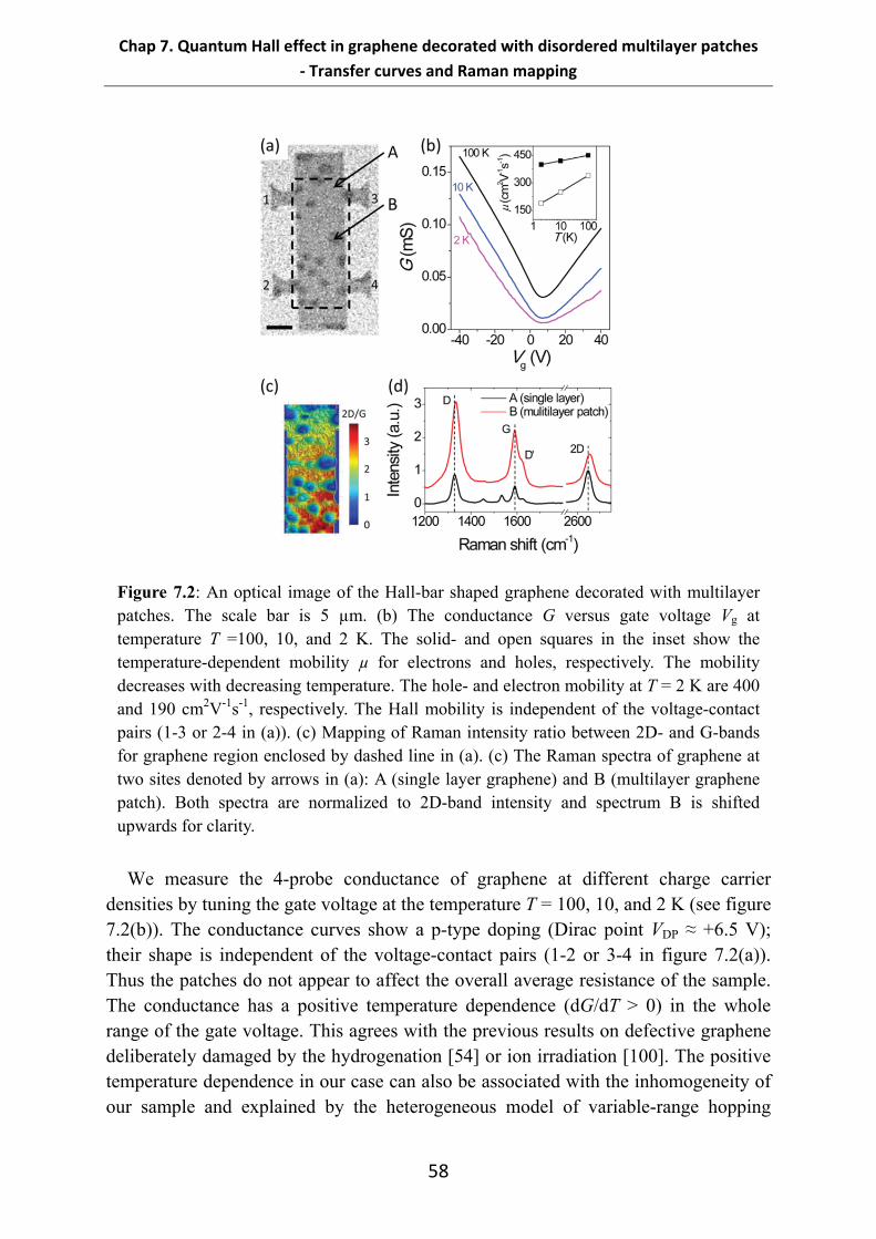
Chap 7. Quantum Hall effect in graphene decorated with disordered multilayer patches
‐ Transfer curves and Raman mapping
58
We measure the 4-probe conductance of graphene at different charge carrier densities by tuning the gate voltage at the temperature T = 100, 10, and 2 K (see figure 7.2(b)). The conductance curves show a p-type doping (Dirac point VDP ≈ +6.5 V); their shape is independent of the voltage-contact pairs (1-2 or 3-4 in figure 7.2(a)). Thus the patches do not appear to affect the overall average resistance of the sample. The conductance has a positive temperature dependence (dG/dT > 0) in the whole range of the gate voltage. This agrees with the previous results on defective graphene deliberately damaged by the hydrogenation [54] or ion irradiation [100]. The positive temperature dependence in our case can also be associated with the inhomogeneity of our sample and explained by the heterogeneous model of variable-range hopping
Figure 7.2: An optical image of the Hall-bar shaped graphene decorated with multilayer patches. The scale bar is 5 µm. (b) The conductance G versus gate voltage Vg at temperature T =100, 10, and 2 K. The solid- and open squares in the inset show the temperature-dependent mobility µ for electrons and holes, respectively. The mobility decreases with decreasing temperature. The hole- and electron mobility at T = 2 K are 400 and 190 cm2V-1s-1, respectively. The Hall mobility is independent of the voltage-contact pairs (1-3 or 2-4 in (a)). (c) Mapping of Raman intensity ratio between 2D- and G-bands for graphene region enclosed by dashed line in (a). (c) The Raman spectra of graphene at two sites denoted by arrows in (a): A (single layer graphene) and B (multilayer graphene patch). Both spectra are normalized to 2D-band intensity and spectrum B is shifted upwards for clarity.
Chap 7. Quantum Hall effect in graphene decorated with disordered multilayer patches
‐ Quantum Hall effect (QHE)
59
where well conducting regions (single layer graphene) are separated by less conducting regions (multilayer patches) [56].
The slope of conductance curves allows for rough estimates of the mobility at different temperatures (see the inset of figure 7.2(b)). In contrast to usually enhanced mobility of graphene at lower temperature, the mobility of this sample decreases with decreasing temperature, which results in the mobility µ ≈ 400 and 190 cm2V-1s-1 at T = 2 K for holes and electrons, respectively. Here, we use a parallel-electrode capacitance model [1]. The Hall mobility for the holes is ≈ 310 cm2V-1S-1, which is comparable with the field-effect result. The mobility attained from the Hall measurement also leads to similar results. It is a very low mobility compared to the previously reported graphene field effect devices in literatures. The low mobility cannot be only attributed to the presence of the defective patches because the distance between them is rather big. Even in the predominantly single-layer areas (region A) the graphene is quite disordered as is seen in the Raman spectra in figure 7.2(d).
In an effort to identify the patch composition, Raman spectroscopy is performed. Figure 7.2(c) indicates mapping of Raman intensity ratio between 2D- and G-bands for graphene region enclosed by dashed line in figure 7.2(a). We find that the intensity ratio of graphene patches (blue round regions) is smaller than one. Figure 7.2(d) shows Raman spectra from different sample parts denoted in figure 7.2(a): A (outside the patch) and B (at the patch). The spot A demonstrates a typical Raman spectrum characteristic for a disordered single layer graphene with except for additional peaks between D and G bands. The peaks can be caused by amorphous (hydrogenated) carbon formed during sample growth or device fabrication [101]. The Raman spectrum in region B displays a much stronger intensity of both D-band (related to the inter-valley scattering process) and D’-band (associated with the intra-valley scattering process in graphene) compared to that of the single layer region A. This indicates that graphene is much more disordered in patch spot B than in single-layer area A. In addition, the spectrum obtained from the patch shows a broader 2D-band accompanied with blue shift (≈ +7.1 cm-1) and lower ratio of I2D to IG. This is consistent with the signature of multi-layer graphene [53]. Therefore, we conclude that the dark patches consist of a defective multi-layer graphene.
7.4 Quantum Hall effect (QHE)
We now turn to QHE measurements. In general, it is known that single-layer graphene shows the half-integer QHE conductance plateaus σxy = ±4(n+1/2)e2/h ≡ νe2/h with the non-negative integer n and filling factors ν = ±2, ±6, ±10…. The integer step of 4 in ν is a manifestation of the four-fold degeneracy of graphene LL owing to the spin- and valley degeneracy. Occasionally, high quality graphene shows other integer ν owing
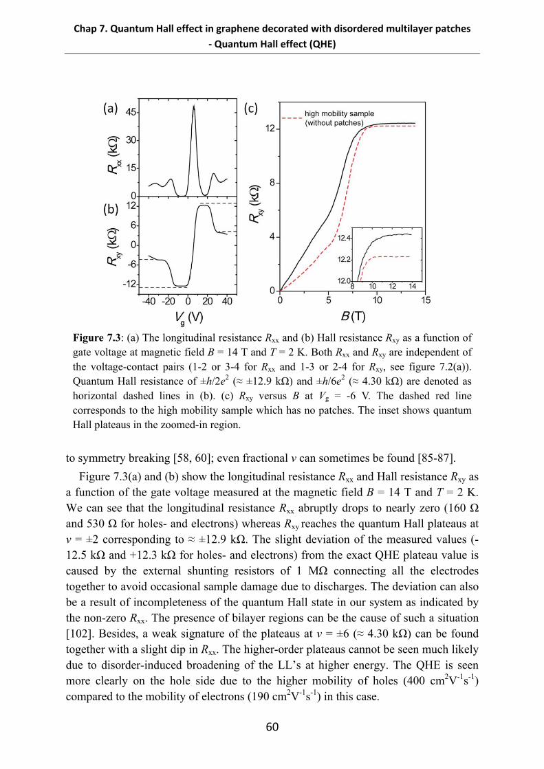
Chap 7. Quantum Hall effect in graphene decorated with disordered multilayer patches
‐ Quantum Hall effect (QHE)
60
to symmetry breaking [58, 60]; even fractional ν can sometimes be found [85-87].
Figure 7.3(a) and (b) show the longitudinal resistance Rxx and Hall resistance Rxy as a function of the gate voltage measured at the magnetic field B = 14 T and T = 2 K. We can see that the longitudinal resistance Rxx abruptly drops to nearly zero (160 Ω and 530 Ω for holes- and electrons) whereas Rxy reaches the quantum Hall plateaus at ν = ±2 corresponding to ≈ ±12.9 kΩ. The slight deviation of the measured values (-12.5 kΩ and +12.3 kΩ for holes- and electrons) from the exact QHE plateau value is caused by the external shunting resistors of 1 MΩ connecting all the electrodes together to avoid occasional sample damage due to discharges. The deviation can also be a result of incompleteness of the quantum Hall state in our system as indicated by the non-zero Rxx. The presence of bilayer regions can be the cause of such a situation [102]. Besides, a weak signature of the plateaus at ν = ±6 (≈ 4.30 kΩ) can be found together with a slight dip in Rxx. The higher-order plateaus cannot be seen much likely due to disorder-induced broadening of the LL’s at higher energy. The QHE is seen more clearly on the hole side due to the higher mobility of holes (400 cm2V-1s-1) compared to the mobility of electrons (190 cm2V-1s-1) in this case.
Figure 7.3: (a) The longitudinal resistance Rxx and (b) Hall resistance Rxy as a function of gate voltage at magnetic field B = 14 T and T = 2 K. Both Rxx and Rxy are independent of the voltage-contact pairs (1-2 or 3-4 for Rxx and 1-3 or 2-4 for Rxy, see figure 7.2(a)). Quantum Hall resistance of ±h/2e2 (≈ ±12.9 kΩ) and ±h/6e2 (≈ 4.30 kΩ) are denoted as horizontal dashed lines in (b). (c) Rxy versus B at Vg = -6 V. The dashed red line corresponds to the high mobility sample which has no patches. The inset shows quantum Hall plateaus in the zoomed-in region.
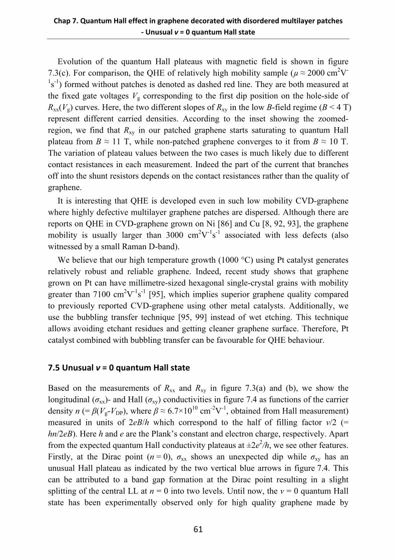
Chap 7. Quantum Hall effect in graphene decorated with disordered multilayer patches
‐ Unusual ν = 0 quantum Hall state
61
Evolution of the quantum Hall plateaus with magnetic field is shown in figure 7.3(c). For comparison, the QHE of relatively high mobility sample (µ ≈ 2000 cm2V-
1s-1) formed without patches is denoted as dashed red line. They are both measured at the fixed gate voltages Vg corresponding to the first dip position on the hole-side of Rxx(Vg) curves. Here, the two different slopes of Rxy in the low B-field regime (B < 4 T) represent different carried densities. According to the inset showing the zoomed-region, we find that Rxy in our patched graphene starts saturating to quantum Hall plateau from B ≈ 11 T, while non-patched graphene converges to it from B ≈ 10 T. The variation of plateau values between the two cases is much likely due to different contact resistances in each measurement. Indeed the part of the current that branches off into the shunt resistors depends on the contact resistances rather than the quality of graphene.
It is interesting that QHE is developed even in such low mobility CVD-graphene where highly defective multilayer graphene patches are dispersed. Although there are reports on QHE in CVD-graphene grown on Ni [86] and Cu [8, 92, 93], the graphene mobility is usually larger than 3000 cm2V-1s-1 associated with less defects (also witnessed by a small Raman D-band).
We believe that our high temperature growth (1000 °C) using Pt catalyst generates relatively robust and reliable graphene. Indeed, recent study shows that graphene grown on Pt can have millimetre-sized hexagonal single-crystal grains with mobility greater than 7100 cm2V-1s-1 [95], which implies superior graphene quality compared to previously reported CVD-graphene using other metal catalysts. Additionally, we use the bubbling transfer technique [95, 99] instead of wet etching. This technique allows avoiding etchant residues and getting cleaner graphene surface. Therefore, Pt catalyst combined with bubbling transfer can be favourable for QHE behaviour.
7.5 Unusual ν = 0 quantum Hall state
Based on the measurements of Rxx and Rxy in figure 7.3(a) and (b), we show the longitudinal (σxx)- and Hall (σxy) conductivities in figure 7.4 as functions of the carrier density n (= β(Vg-VDP), where β ≈ 6.7×1010 cm-2V-1, obtained from Hall measurement) measured in units of 2eB/h which correspond to the half of filling factor ν/2 (= hn/2eB). Here h and e are the Plank’s constant and electron charge, respectively. Apart from the expected quantum Hall conductivity plateaus at ±2e2/h, we see other features. Firstly, at the Dirac point (n = 0), σxx shows an unexpected dip while σxy has an unusual Hall plateau as indicated by the two vertical blue arrows in figure 7.4. This can be attributed to a band gap formation at the Dirac point resulting in a slight splitting of the central LL at n = 0 into two levels. Until now, the ν = 0 quantum Hall state has been experimentally observed only for high quality graphene made by
Chap 7. Quantum Hall effect in graphene decorated with disordered multilayer patches
‐ Conclusions
62
mechanical exfoliation [58-62]. This state is normally explained by the spin-valley symmetry breaking which lifts the degeneracy of LL [58, 62], counter-propagating edge states [59], and gap opening in the magnetic field [60, 61]. We believe that our case is rather due to the disorder induced gap opening [64-66] resulting from the defective multilayer graphene patches. In fact, we also observed the same behaviour of the QHE in wrinkled CVD-graphene grown on Cu (in chapter 5).
Moreover, the centre of the dip (in σxx) and plateau (in σxy) are somewhat shifted from the anticipated positions ν = ±2 denoted by the vertical dashed lines. This can be attributed to a pool of localized states which do not contribute to the degeneracy of LL [103]. The localized states are situated between LL’s and result in a “delay” when filling LL’s by increasing carrier density. Here, the spatially distributed graphene patches probably act as origin of the localized states.
7.6 Conclusions
We have observed the QHE in CVD-graphene grown on platinum. The QHE is even seen in samples which are irregularly decorated with disordered multilayer graphene patches and have very low mobility (< 500 cm2V-1s-1). The QHE does not appear to depend on electronic mobility and uniformity of the resulting material. This emphasizes the robustness of QHE in Pt used CVD-graphene.
Figure 7.4: The longitudinal conductivity σxx (black lines) and Hall conductivity σxy (red lines) versus the carrier density n. They are calculated using Rxx and Rxy in figure 7.3(a) and (b). The n corresponding to filling factor ν = ±2 are denoted as vertical dashed lines. Two vertical blue arrows indicates unusual dip (in σxx) and plateau (in σxy) at n = 0.
Chap 8. Summary
63
Chapter 8
8. Summary
We performed electronic transport experiments on graphene with the Aharonov-Bohm (AB) effect, thermopower (TEP) measurements, dual-gated graphene field effect devices, and quantum Hall effect (QHE).
To enhance the AB effect, we locate superconducting-metal (aluminium) or normal-metal (gold) mirrors on the graphene rings. The mirrors are positioned either in the transverse or in the longitudinal direction with respect to the ring bias lines. A significant enhancement of the phase coherence effect is confirmed in the latter case from the observation of the third harmonic of the AB oscillations. The superconducting contribution to the AB effect by the aluminium (Al) mirrors is unclear. Instead, we believe that a large mismatch of Fermi velocity between graphene and the mirror materials can account for the enhancement.
Secondly, a TEP measurement is performed to investigate the electronic properties of inhomogeneous graphene grown by chemical vapour deposition (CVD). The gate-dependent TEP shows a large electron-hole asymmetry probably due to the inhomogeneity of CVD-graphene where individual graphene regions provide different TEP. In high magnetic field and low temperature, we observe anomalously large TEP fluctuations and an insulating quantum Hall state near the Dirac point, which could be associated with the disorder-induced energy gap opening.
Thirdly, graphene field effect devices are made using two gates; top- and back-gates. The top gate is made of Al deposited onto the middle part of the graphene channel. We found that naturally formed Al2O3 at the interface between graphene and the Al top-gate can be facilitated for a top-gate dielectric layer. By tuning both gate voltages simultaneously, graphene p-n-p junctions are achieved. Additionally when the Al top-gate is floating, a double-peak accompanied by hysteresis appears in the graphene resistance with respect to the slowly-varying back-gate voltage. This could indicate an Al doping effect and the coupling between the two gates.
Lastly, We have observed the QHE in CVD-graphene grown on platinum. The QHE is even seen in samples which are irregularly decorated with disordered multilayer graphene patches and have very low mobility (< 500 cm2V-1s-1). The QHE does not appear to depend on electronic mobility and uniformity of the resulting material. This emphasizes the robustness of QHE in Pt catalyzed CVD-graphene.

64
Acknowledgements
65
Acknowledgements
I came to Chalmers, Sweden in 2009 as a guest PhD student while I was doing my 4th year integrated MA/PhD program in Seoul National University (SNU), Korea. The visit was preliminarily planned for two years but luckily since 2012 I have started another PhD program in Chalmers in accordance with the agreement between Chalmers and SNU, establishing double degrees. When I first entered graphene research in Chalmers, I barely had any experience in microfabrication inside the clean-room which was necessary for making graphene devices in this thesis work. I had to learn many things from scratch. I would like to recollect people who have helped me to finally achieve my thesis work in Chalmers and express them my warmest gratitude.
First of all, I would like to thank my supervisor, August Yurgens. He showed me many ideas and insights throughout my thesis work. Moreover, he helped me in conducting measurements and correcting manuscripts for the publication in the scientific journal. Indeed, I can publish my first-authored articles as a result of the work carried out here.
I wish to express my gratitude to my co-supervisor, Jie Sun and my colleague, Niclas Lindvall. Like me, they have devoted themselves to graphene research in August’s group. I benefited greatly from their knowledge. In particular, Jie provided me with CVD-graphene samples and he later taught me graphene growth techniques using a CVD-machine together with its growth mechanism. This allowed me to expand the scope of my research. Niclas taught me many clean-room tools and he also helped me by actively participating in the sample preparation and measurements throughout much of my thesis work.
I would like to thank my supervisor, Yung Woo Park at SNU for his guidance and support. He gave me the opportunity to work in the Quantum Device Physics laboratory (QDP) in MC2 and financially supported my living expenses. When I first visited QDP in 2009, there were two previous PhD students, Jae Seung Yoo and Seung Joo Park who also came from Park’s group. I would like to show my appreciation to them for sharing their experiment know-how and knowledge of how to live in Sweden.
I am also grateful to the colleagues in QDP as well as the clean-room staff members for their assistance. I sincerely wish them the best of luck.
Lastly, I would like to express thanks to my parents and sister for their affectionate support.

66
References
67
References
[1] Novoselov KS, Geim AK, Morozov SV, Jiang D, Zhang Y, Dubonos SV, et al. Electric Field Effect in Atomically Thin Carbon Films. Science. 2004;306(5696):666-9.
[2] Novoselov KS, Jiang D, Schedin F, Booth TJ, Khotkevich VV, Morozov SV, et al. Two-dimensional atomic crystals. Proceedings of the National Academy of Sciences of the United States of America. 2005;102(30):10451-3.
[3] Novoselov KS, Geim AK, Morozov SV, Jiang D, Katsnelson MI, Grigorieva IV, et al. Two-dimensional gas of massless Dirac fermions in graphene. Nature. 2005;438(7065):197-200.
[4] Zhang Y, Tan Y-W, Stormer HL, Kim P. Experimental observation of the quantum Hall effect and Berry's phase in graphene. Nature. 2005;438(7065):201-4.
[5] Katsnelson MI, Novoselov KS, Geim AK. Chiral tunnelling and the Klein paradox in graphene. Nat Phys. 2006;2(9):620-5.
[6] Young AF, Kim P. Quantum interference and Klein tunnelling in graphene heterojunctions. Nat Phys. 2009;5(3):222-6.
[7] Lin Y-M, Dimitrakopoulos C, Jenkins KA, Farmer DB, Chiu H-Y, Grill A, et al. 100-GHz Transistors from Wafer-Scale Epitaxial Graphene. Science. 2010;327(5966):662.
[8] Bae S, Kim H, Lee Y, Xu X, Park J-S, Zheng Y, et al. Roll-to-roll production of 30-inch graphene films for transparent electrodes. Nat Nano. 2010;5(8):574-8.
[9] Kim KS, Zhao Y, Jang H, Lee SY, Kim JM, Kim KS, et al. Large-scale pattern growth of graphene films for stretchable transparent electrodes. Nature. 2009;457(7230):706-10.
[10] Li X, Cai W, An J, Kim S, Nah J, Yang D, et al. Large-Area Synthesis of High-Quality and Uniform Graphene Films on Copper Foils. Science. 2009;324(5932):1312-4.
[11] Washburn S, Webb RA. Aharonov-Bohm effect in normal metal quantum coherence and transport. Advances in Physics. 1986;35(4):375 - 422.
[12] Beenakker CWJ, van Houten H, Henry E, David T. Quantum Transport in Semiconductor Nanostructures. Solid State Physics: Academic Press 1991, p. 1-228.
[13] Hansen AE, Kristensen A, Pedersen S, Sørensen CB, Lindelof PE. Mesoscopic decoherence in Aharonov-Bohm rings. Physical Review B. 2001;64(4):045327.
[14] Giovannetti G, Khomyakov PA, Brocks G, Karpan VM, van den Brink J, Kelly PJ. Doping Graphene with Metal Contacts. Physical Review Letters. 2008;101(2):026803.
[15] Khomyakov PA, Giovannetti G, Rusu PC, Brocks G, van den Brink J, Kelly PJ. First-principles study of the interaction and charge transfer between graphene and metals. Physical Review B. 2009;79(19):195425.
[16] Park N, Kim B-K, Lee J-O, Kim J-J. Influence of metal work function on the position of the Dirac point of graphene field-effect transistors. Applied Physics Letters. 2009;95(24):243105-3.
[17] Malec CE, Davidovic D. Transport in graphene tunnel junctions. Journal of Applied Physics. 2011;109(6):064507-8.
[18] Blake P, Hill EW, Neto AHC, Novoselov KS, Jiang D, Yang R, et al. Making graphene visible. Applied Physics Letters. 2007;91(6):063124-3.
References
68
[19] Gao L, Ren W, Li F, Cheng H-M. Total Color Difference for Rapid and Accurate Identification of Graphene. ACS Nano. 2008;2(8):1625-33.
[20] Lei L, et al. Single-layer graphene on Al 2 O 3 /Si substrate: better contrast and higher performance of graphene transistors. Nanotechnology. 2010;21(1):015705.
[21] Marco PD, et al. Rapid identification of graphene flakes: alumina does it better. Nanotechnology. 2010;21(25):255703.
[22] Jie S, Lindvall N, Cole MT, Angel KTT, Teng W, Teo KBK, et al. Low Partial Pressure Chemical Vapor Deposition of Graphene on Copper. IEEE Trans Nanotechnol. 2012;11(2):255-60.
[23] Hansen AE, Kristensen A, Pedersen S, Sorensen CB, Lindelof PE. Mesoscopic decoherence in Aharonov-Bohm rings. Physical Review B. 2001;64(4):045327.
[24] Bolotin KI, Sikes KJ, Hone J, Stormer HL, Kim P. Temperature-Dependent Transport in Suspended Graphene. Physical Review Letters. 2008;101(9):096802.
[25] Du X, Skachko I, Barker A, Andrei EY. Approaching ballistic transport in suspended graphene. Nat Nano. 2008;3(8):491-5.
[26] Russo S, Oostinga JB, Wehenkel D, Heersche HB, Sobhani SS, Vandersypen LMK, et al. Observation of Aharonov-Bohm conductance oscillations in a graphene ring. Physical Review B. 2008;77(8):085413.
[27] Huefner M, Molitor F, Jacobsen A, Pioda A, Stampfer C, Ensslin K, et al. The Aharonov-Bohm effect in a side-gated graphene ring. New Journal of Physics. 2010;12(4):043054.
[28] Huefner M, Molitor F, Jacobsen A, Pioda A, Stampfer C, Ensslin K, et al. Investigation of the Aharonov-Bohm effect in a gated graphene ring. Phys Status Solidi B-Basic Solid State Phys. 2009;246(11-12):2756-9.
[29] Yoo JS, Park YW, Skakalova V, Roth S. Shubnikov-de Haas and Aharonov Bohm effects in a graphene nanoring structure. Applied Physics Letters. 2010;96(14):3.
[30] Smirnov D, Schmidt H, Haug RJ. Aharonov-Bohm effect in an electron-hole graphene ring system. Applied Physics Letters. 2012;100(20):203114-3.
[31] Petrashov VT, Antonov VN, Delsing P, Claeson R. Phase memory effects in mesoscopic rings with superconducting ``mirrors''. Physical Review Letters. 1993;70(3):347.
[32] Petrashov VT, Antonov VN, Shaikhaidarov RS, Maksimov SV, Meeson P, Souhami R, et al. "Giant" Aharonov-Bohm effect in mesoscopic silver rings with bismuth electrodes. EPL (Europhysics Letters). 1996;34(8):593.
[33] Han MY, Brant JC, Kim P. Electron Transport in Disordered Graphene Nanoribbons. Physical Review Letters. 2010;104(5):056801.
[34] Han MY, Yilmaz B, Zhang Y, Kim P. Energy Band-Gap Engineering of Graphene Nanoribbons. Physical Review Letters. 2007;98(20):206805.
[35] Stampfer C, Gütinger J, Hellmüler S, Molitor F, Ensslin K, Ihn T. Energy Gaps in Etched Graphene Nanoribbons. Physical Review Letters. 2009;102(5):056403.
[36] Oostinga JB, Sacepe B, Craciun MF, Morpurgo AF. Magneto-transport through graphene nano-ribbons. arXiv:10032994v1. 2010.
[37] Sols F, Guinea F, Neto AHC. Coulomb Blockade in Graphene Nanoribbons. Physical Review Letters. 2007;99(16):166803.
References
69
[38] McCann E, Kechedzhi K, Fal'ko VI, Suzuura H, Ando T, Altshuler BL. Weak-Localization Magnetoresistance and Valley Symmetry in Graphene. Physical Review Letters. 2006;97(14):146805.
[39] Löfwander T, Fogelström M. Impurity scattering and Mott’s formula in graphene. Physical Review B. 2007;76(19):193401.
[40] Hwang EH, Rossi E, Das Sarma S. Theory of thermopower in two-dimensional graphene. Physical Review B. 2009;80(23):235415.
[41] Zhu L, Ma R, Sheng L, Liu M, Sheng D-N. Universal Thermoelectric Effect of Dirac Fermions in Graphene. Physical Review Letters. 2010;104(7):076804.
[42] Zuev YM, Chang W, Kim P. Thermoelectric and Magnetothermoelectric Transport Measurements of Graphene. Physical Review Letters. 2009;102(9):096807.
[43] Wei P, Bao W, Pu Y, Lau CN, Shi J. Anomalous Thermoelectric Transport of Dirac Particles in Graphene. Physical Review Letters. 2009;102(16):166808.
[44] Checkelsky JG, Ong NP. Thermopower and Nernst effect in graphene in a magnetic field. Physical Review B. 2009;80(8):081413.
[45] Wang D, Shi J. Effect of charged impurities on the thermoelectric power of graphene near the Dirac point. Physical Review B. 2011;83(11):113403.
[46] Wu X, Hu Y, Ruan M, Madiomanana NK, Berger C, de Heer WA. Thermoelectric effect in high mobility single layer epitaxial graphene. Applied Physics Letters. 2011;99(13):133102-3.
[47] Yin J, Zhou J, Li X, Chen Y, Tai G, Guo W. Enhanced gas-flow-induced voltage in graphene. Applied Physics Letters. 2011;99(7):073103-3.
[48] Sidorov AN, Sherehiy A, Jayasinghe R, Stallard R, Benjamin DK, Yu Q, et al. Thermoelectric power of graphene as surface charge doping indicator. Applied Physics Letters. 2011;99(1):013115-3.
[49] Xiao N, Dong X, Song L, Liu D, Tay Y, Wu S, et al. Enhanced Thermopower of Graphene Films with Oxygen Plasma Treatment. ACS Nano. 2011;5(4):2749-55.
[50] Jie S, Lindvall N, Cole MT, Angel KTT, Teng W, Teo KBK, et al. Low Partial Pressure Chemical Vapor Deposition of Graphene on Copper. Nanotechnology, IEEE Transactions on. 2012;11(2):255-60.
[51] Small JP, Shi L, Kim P. Mesoscopic thermal and thermoelectric measurements of individual carbon nanotubes. Solid State Communications. 2003;127(2):181-6.
[52] Yu Q, Jauregui LA, Wu W, Colby R, Tian J, Su Z, et al. Control and characterization of individual grains and grain boundaries in graphene grown by chemical vapour deposition. Nat Mater. 2011;10(6):443-9.
[53] Martins Ferreira EH, Moutinho MVO, Stavale F, Lucchese MM, Capaz RB, Achete CA, et al. Evolution of the Raman spectra from single-, few-, and many-layer graphene with increasing disorder. Phys Rev B. 2010;82(12):125429.
[54] Elias DC, Nair RR, Mohiuddin TMG, Morozov SV, Blake P, Halsall MP, et al. Control of Graphene's Properties by Reversible Hydrogenation: Evidence for Graphane. Science. 2009;323(5914):610-3.
[55] Eckmann A, Felten A, Mishchenko A, Britnell L, Krupke R, Novoselov KS, et al. Probing the Nature of Defects in Graphene by Raman Spectroscopy. Nano Letters. 2012.
References
70
[56] Kaiser AB, Gómez-Navarro C, Sundaram RS, Burghard M, Kern K. Electrical Conduction Mechanism in Chemically Derived Graphene Monolayers. Nano Lett. 2009;9(5):1787-92.
[57] Cho S, Kang SD, Kim W, Lee E-S, Woo S-J, Kong K-J, et al. Thermoelectric imaging of structural disorder in epitaxial graphene. Nat Mater. 2013;advance online publication.
[58] Zhang Y, Jiang Z, Small JP, Purewal MS, Tan YW, Fazlollahi M, et al. Landau-Level Splitting in Graphene in High Magnetic Fields. Phys Rev Lett. 2006;96(13):136806.
[59] Abanin DA, Novoselov KS, Zeitler U, Lee PA, Geim AK, Levitov LS. Dissipative Quantum Hall Effect in Graphene near the Dirac Point. Phys Rev Lett. 2007;98(19):196806.
[60] Checkelsky JG, Li L, Ong NP. Zero-Energy State in Graphene in a High Magnetic Field. Phys Rev Lett. 2008;100(20):206801.
[61] Zhang L, Zhang Y, Khodas M, Valla T, Zaliznyak IA. Metal to Insulator Transition on the N=0 Landau Level in Graphene. Phys Rev Lett. 2010;105(4):046804.
[62] Zhao Y, Cadden-Zimansky P, Ghahari F, Kim P. Magnetoresistance Measurements of Graphene at the Charge Neutrality Point. Phys Rev Lett. 2012;108(10):106804.
[63] Bai J, Zhong X, Jiang S, Huang Y, Duan X. Graphene nanomesh. Nat Nano. 2010;5(3):190-4.
[64] Yang C-K. Graphane with defect or transition-metal impurity. Carbon. 2010;48(13):3901-5.
[65] Pujari BS, Kanhere DG. Density Functional Investigations of Defect-Induced Mid-Gap States in Graphane. J Phys Chem C. 2009;113(50):21063-7.
[66] Amirhasan N, Mirco C, Tom V, Geoffrey P, Francesca C, Marleen HvdV, et al. Bandgap opening in oxygen plasma-treated graphene. Nanotechnology. 2010;21(43):435203.
[67] Sharapov SG, Varlamov AA. Anomalous growth of thermoelectric power in gapped graphene. Physical Review B. 2012;86(3):035430.
[68] Patel AA, Mukerjee S. Thermoelectricity in graphene: Effects of a gap and magnetic fields. Physical Review B. 2012;86(7):075411.
[69] Wang C-R, Lu W-S, Hao L, Lee W-L, Lee T-K, Lin F, et al. Enhanced Thermoelectric Power in Dual-Gated Bilayer Graphene. Physical Review Letters. 2011;107(18):186602.
[70] Williams JR, DiCarlo L, Marcus CM. Quantum Hall Effect in a Gate-Controlled p-n Junction of Graphene. Science. 2007;317(5838):638-41.
[71] Ouml, zyilmaz B, Jarillo-Herrero P, Efetov D, Abanin DA, Levitov LS, et al. Electronic Transport and Quantum Hall Effect in Bipolar Graphene p-n-p Junctions. Physical Review Letters. 2007;99(16):166804.
[72] Huard B, Sulpizio JA, Stander N, Todd K, Yang B, Goldhaber-Gordon D. Transport Measurements Across a Tunable Potential Barrier in Graphene. Physical Review Letters. 2007;98(23):236803.
[73] Liu G, Velasco JJ, Bao W, Lau CN. Fabrication of graphene p-n-p junctions with contactless top gates. Applied Physics Letters. 2008;92(20):203103-3.
[74] Tian JF, Jauregui LA, Lopez G, Cao H, Chen YP. Ambipolar graphene field effect transistors by local metal side gates. Applied Physics Letters. 2010;96(26):263110-3.
[75] Farmer DB, Lin Y-M, Afzali-Ardakani A, Avouris P. Behavior of a chemically doped graphene junction. Applied Physics Letters. 2009;94(21):213106-3.
References
71
[76] Lohmann T, von Klitzing K, Smet JH. Four-Terminal Magneto-Transport in Graphene p-n Junctions Created by Spatially Selective Doping. Nano Letters. 2009;9(5):1973-9.
[77] Brenner K, Murali R. Single step, complementary doping of graphene. Applied Physics Letters. 2010;96(6):063104-3.
[78] Hisao Miyazaki SO, Takashi Sato, Sho Tanaka, Hidenori Goto, Akinobu Kanda, Kazuhito Tsukagoshi Youiti Ootuka, and Yoshinobu Aoyagi. Inter-Layer Screening Length to Electric Field in Thin Graphite Film. Applied Physics Express. 2008;1(3):3.
[79] Robinson JA, LaBella M, Zhu M, Hollander M, Kasarda R, Hughes Z, et al. Contacting graphene. Applied Physics Letters. 2011;98(5):053103-3.
[80] Kim S, Nah J, Jo I, Shahrjerdi D, Colombo L, Yao Z, et al. Realization of a high mobility dual-gated graphene field-effect transistor with Al[sub 2]O[sub 3] dielectric. Applied Physics Letters. 2009;94(6):062107-3.
[81] Xia JL, Chen F, Wiktor P, Ferry DK, Tao NJ. Effect of Top Dielectric Medium on Gate Capacitance of Graphene Field Effect Transistors: Implications in Mobility Measurements and Sensor Applications. Nano Letters. 2010;10(12):5060-4.
[82] Chiu H-Y, Perebeinos V, Lin Y-M, Avouris P. Controllable p-n Junction Formation in Monolayer Graphene Using Electrostatic Substrate Engineering. Nano Letters. 2010;10(11):4634-9.
[83] Klitzing Kv, Dorda G, Pepper M. New Method for High-Accuracy Determination of the Fine-Structure Constant Based on Quantized Hall Resistance. Phys Rev Lett. 1980;45(6):494-7.
[84] Ando T, Fowler AB, Stern F. Electronic properties of two-dimensional systems. Rev Mod Phys. 1982;54(2):437-672.
[85] Du X, Skachko I, Duerr F, Luican A, Andrei EY. Fractional quantum Hall effect and insulating phase of Dirac electrons in graphene. Nature. 2009;462(7270):192-5.
[86] Bolotin KI, Ghahari F, Shulman MD, Stormer HL, Kim P. Observation of the fractional quantum Hall effect in graphene. Nature. 2009;462(7270):196-9.
[87] Dean CR, Young AF, Cadden-Zimansky P, Wang L, Ren H, Watanabe K, et al. Multicomponent fractional quantum Hall effect in graphene. Nat Phys. 2011;7(9):693-6.
[88] Novoselov KS, Jiang Z, Zhang Y, Morozov SV, Stormer HL, Zeitler U, et al. Room-Temperature Quantum Hall Effect in Graphene. Science. 2007;315(5817):1379.
[89] Arapov YG, Harus GI, Karskanov IV, Neverov VN, Shelushinina NG, Yakunin MV, et al. Quantum Hall effect in p-Ge/Ge[sub 1 - x]Si[sub x] heterostructures with low hole mobility. Low Temp Phys. 2007;33(2):147-50.
[90] Liang C-T, Lin L-H, Kuang Yoa C, Lo S-T, Wang Y-T, Lou D-S, et al. On the direct insulator-quantum Hall transition in two-dimensional electron systems in the vicinity of nanoscaled scatterers. Nanoscale Res Lett. 2011;6(1):131.
[91] Pallecchi E, Ridene M, Kazazis D, Lafont F, Schopfer F, Poirier W, et al. Insulating to relativistic quantum Hall transition in disordered graphene. Sci Rep. 2013;3.
[92] Cao H, Yu Q, Jauregui LA, Tian J, Wu W, Liu Z, et al. Electronic transport in chemical vapor deposited graphene synthesized on Cu: Quantum Hall effect and weak localization. Appl Phys Lett. 2010;96(12):122106-3.
References
72
[93] Shen T, Wu W, Yu Q, Richter CA, Elmquist R, Newell D, et al. Quantum Hall effect on centimeter scale chemical vapor deposited graphene films. Appl Phys Lett. 2011;99(23):232110-3.
[94] Sutter P, Sadowski JT, Sutter E. Graphene on Pt(111): Growth and substrate interaction. Phys Rev B. 2009;80(24):245411.
[95] Gao L, Ren W, Xu H, Jin L, Wang Z, Ma T, et al. Repeated growth and bubbling transfer of graphene with millimetre-size single-crystal grains using platinum. Nat Commun. 2012;3:699.
[96] Xu H, Zhang Z, Shi R, Liu H, Wang Z, Wang S, et al. Batch-fabricated high-performance graphene Hall elements. Sci Rep. 2013;3.
[97] Shi R, Xu H, Chen B, Zhang Z, Peng L-M. Scalable fabrication of graphene devices through photolithography. Appl Phys Lett. 2013;102(11):113102-5.
[98] Jinglei Ping MSF. Carbon Impurities on Graphene Synthesized by Chemical Vapor Deposition on Platinum. arXiv:13045123. 2013.
[99] de la Rosa CJL, Sun J, Lindvall N, Cole MT, Nam Y, Loffler M, et al. Frame assisted H[sub 2]O electrolysis induced H[sub 2] bubbling transfer of large area graphene grown by chemical vapor deposition on Cu. Appl Phys Lett. 2013;102(2):022101-4.
[100] Chen J-H, Cullen WG, Jang C, Fuhrer MS, Williams ED. Defect Scattering in Graphene. Phys Rev Lett. 2009;102(23):236805.
[101] Hong J, Park MK, Lee EJ, Lee D, Hwang DS, Ryu S. Origin of New Broad Raman D and G Peaks in Annealed Graphene. Sci Rep. 2013;3.
[102] Löfwander T, San-Jose P, Prada E. Quantum Hall effect in graphene with twisted bilayer stripe defects. Phys Rev B. 2013;87(20):205429.
[103] Lee DS, Riedl C, Beringer T, Castro Neto AH, von Klitzing K, Starke U, et al. Quantum Hall Effect in Twisted Bilayer Graphene. Phys Rev Lett. 2011;107(21):216602.