Embed Size (px)
Citation preview
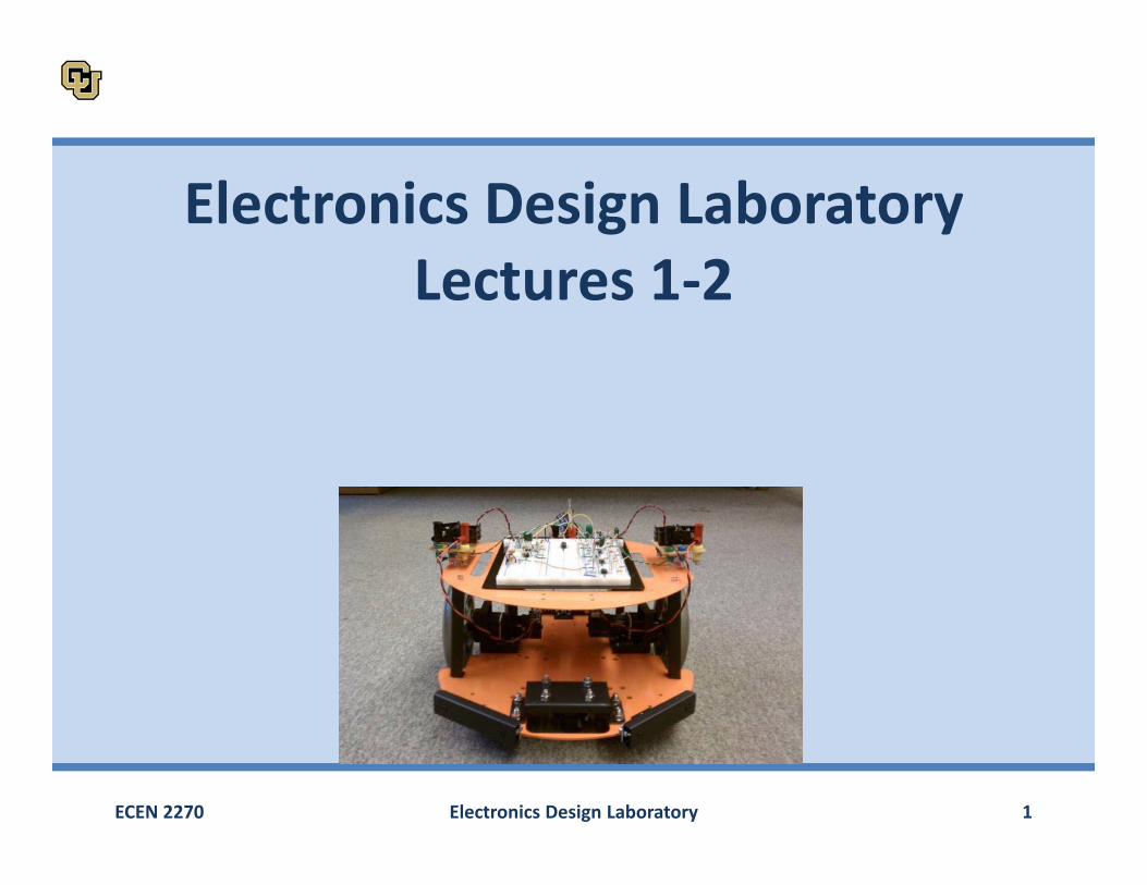
Electronics Design LaboratoryLectures 1‐2
ECEN 2270 1Electronics Design Laboratory
Prerequisites and Co‐requisites
• Lectures: Monday • Labs: Tuesday and Thursday (ECEE281/282)
Electronics Design Laboratory 2ECEN 2270
• Prerequisite: ECEN2250 Intro to Circuits & Electronics• Co‐requisite: ECEN2260 Circuits as Systems
Meetings
• Attendance in the lab and the lectures is REQUIRED to receive any credit
• In the lab: no food or drinks; no music; no social networking; no browsing of unrelated sites; no exceptions!
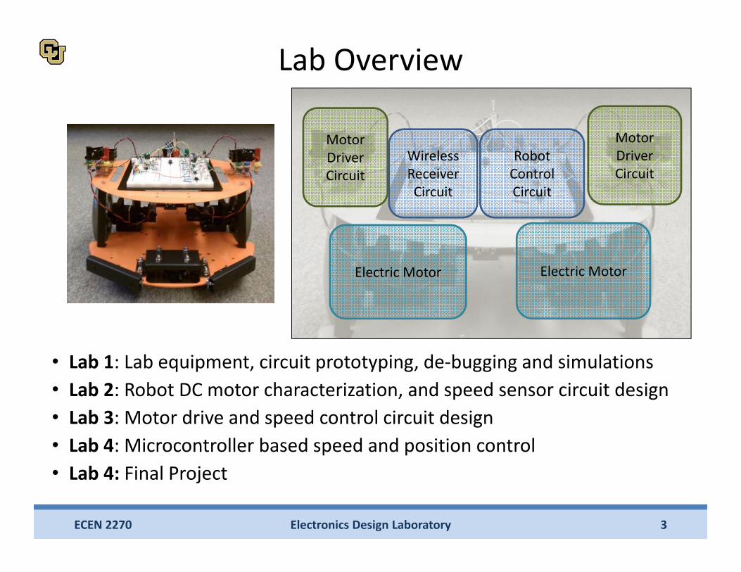
Lab Overview
• Lab 1: Lab equipment, circuit prototyping, de‐bugging and simulations• Lab 2: Robot DC motor characterization, and speed sensor circuit design• Lab 3: Motor drive and speed control circuit design• Lab 4: Microcontroller based speed and position control• Lab 4: Final Project
Electronics Design Laboratory 3ECEN 2270
WirelessReceiverCircuit
Robot Control Circuit
Motor DriverCircuit
Electric Motor Electric Motor
Motor DriverCircuit
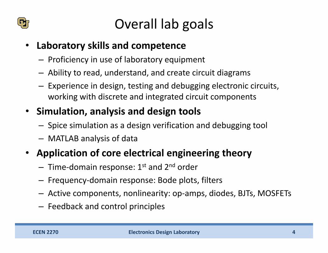
Overall lab goals• Laboratory skills and competence
– Proficiency in use of laboratory equipment– Ability to read, understand, and create circuit diagrams– Experience in design, testing and debugging electronic circuits,
working with discrete and integrated circuit components
• Simulation, analysis and design tools– Spice simulation as a design verification and debugging tool– MATLAB analysis of data
• Application of core electrical engineering theory– Time‐domain response: 1st and 2nd order– Frequency‐domain response: Bode plots, filters– Active components, nonlinearity: op‐amps, diodes, BJTs, MOSFETs– Feedback and control principles
Electronics Design Laboratory 4ECEN 2270
Organization• Lab Rules: standard ECEE Lab rules apply• Teams Teams of Students (2 or 3 per team, instructor will announce) + 1 Robot
Begin working in teams from the first lab session; teams remain the same throughout the semester
• Purchase Lab kits (one per team) Component kit ($160‐ish); tools kit: ($70‐ish), you may already have it Purchase at the EE Store, ECEE 1B10
• Assignments Prelab assignment due in lab (hard copy), individually Quizzes in lectures (hard copy), individually Lab reports (soft copy) due on D2L, team
• If you have issues Lab computer access, ECES student server: http://eces.colorado.edu
Talk to ECEE IT staff if you have issues Lab card access will be enabled once you sign on the Lab use agreement
Talk to ECEE front desk if you have issues Instructor/TA about anything else
Electronics Design Laboratory 5ECEN 2270
Grading• In‐class quizzes [individual], 15%• Labs 1‐4, 60%
– Pre‐labs [individual]– Demonstrations [team and individual]– Reports [team]
• Final project, 20%– Proposal slides and presentation [team]– Proposal write‐up [team]– Expo [team and individual]– Report [team]
• Lab attendance and performance [individual], 5%
Electronics Design Laboratory 6ECEN 2270
Attendance in the lab and the lectures is required to receive any credit
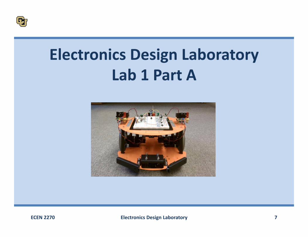
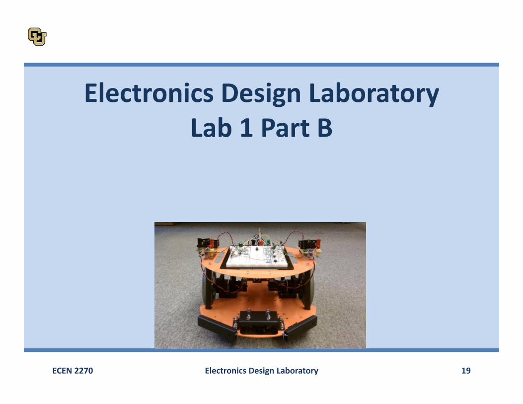
Electronics Design LaboratoryLab 1 Part A
ECEN 2270 7Electronics Design Laboratory
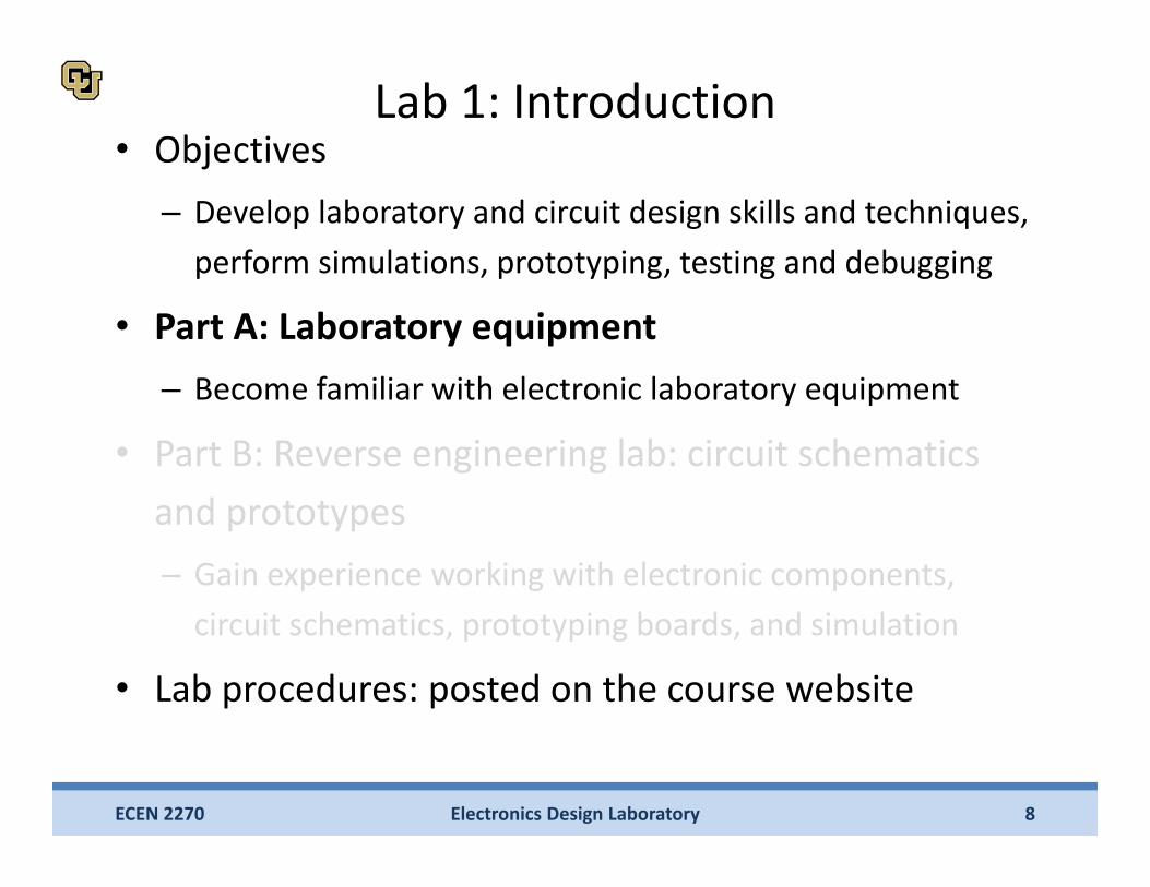
Lab 1: Introduction• Objectives
– Develop laboratory and circuit design skills and techniques, perform simulations, prototyping, testing and debugging
• Part A: Laboratory equipment– Become familiar with electronic laboratory equipment
• Part B: Reverse engineering lab: circuit schematics and prototypes– Gain experience working with electronic components, circuit schematics, prototyping boards, and simulation
• Lab procedures: posted on the course website
Electronics Design Laboratory 8ECEN 2270
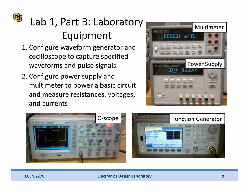
Lab 1, Part B: Laboratory Equipment
1. Configure waveform generator and oscilloscope to capture specified waveforms and pulse signals
2. Configure power supply and multimeter to power a basic circuit and measure resistances, voltages, and currents
Electronics Design Laboratory 9ECEN 2270
O‐scope Function Generator
Power Supply
Multimeter
Electronics Design Laboratory 10ECEN 2270
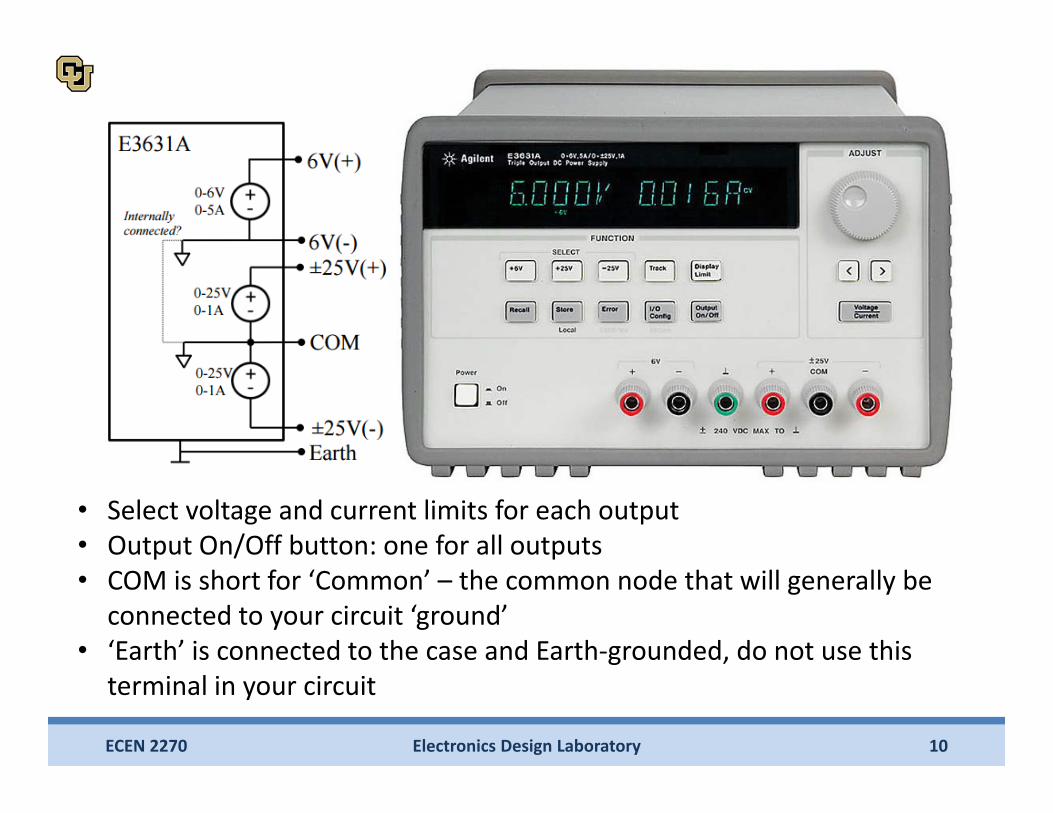
• Select voltage and current limits for each output• Output On/Off button: one for all outputs• COM is short for ‘Common’ – the common node that will generally be
connected to your circuit ‘ground’• ‘Earth’ is connected to the case and Earth‐grounded, do not use this
terminal in your circuit
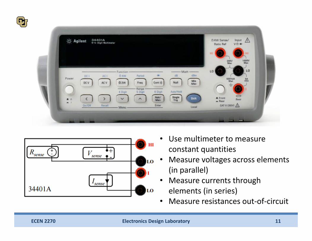
Electronics Design Laboratory 11ECEN 2270
• Use multimeter to measure constant quantities
• Measure voltages across elements (in parallel)
• Measure currents through elements (in series)
• Measure resistances out‐of‐circuit
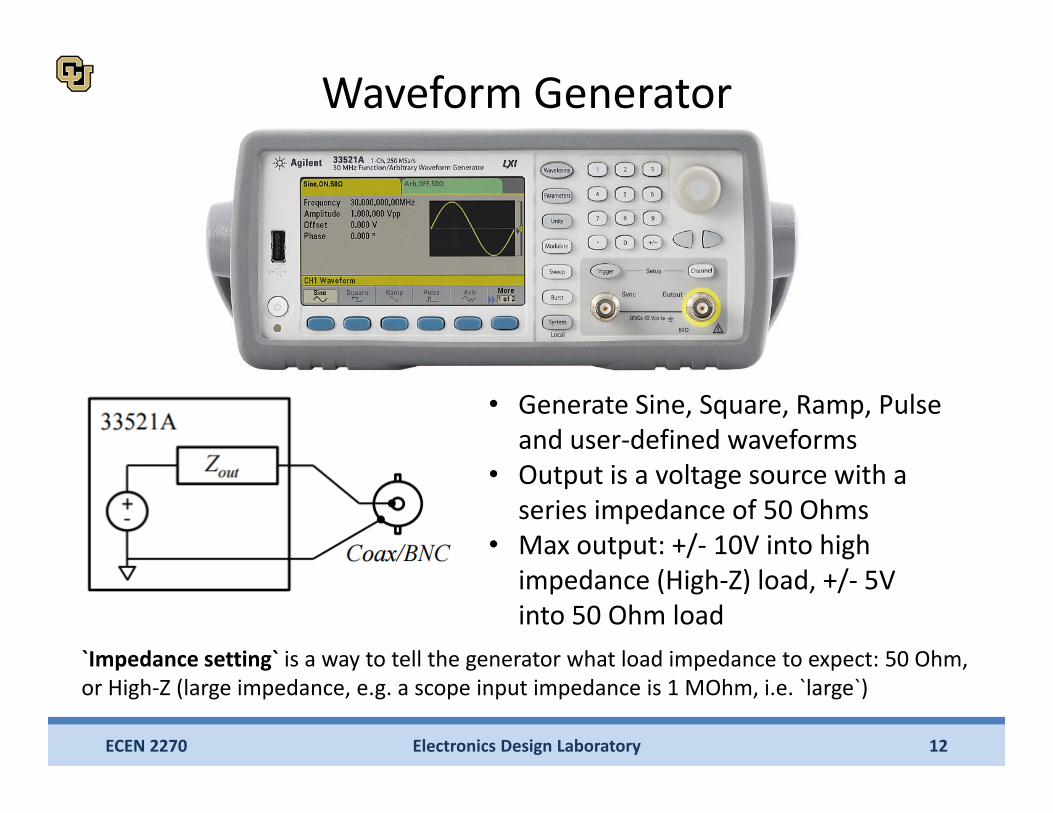
Waveform Generator
Electronics Design Laboratory 12ECEN 2270
• Generate Sine, Square, Ramp, Pulse and user‐defined waveforms
• Output is a voltage source with a series impedance of 50 Ohms
• Max output: +/‐ 10V into high impedance (High‐Z) load, +/‐ 5V into 50 Ohm load
`Impedance setting` is a way to tell the generator what load impedance to expect: 50 Ohm, or High‐Z (large impedance, e.g. a scope input impedance is 1 MOhm, i.e. `large`)
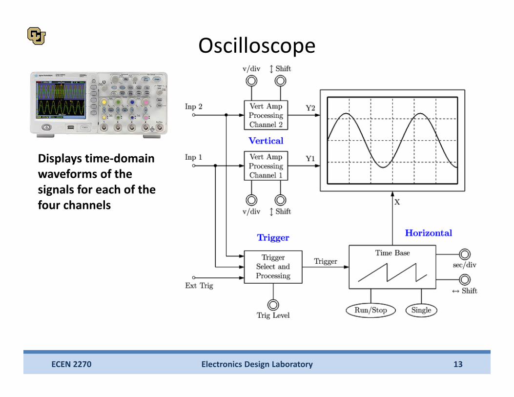
Oscilloscope
Electronics Design Laboratory 13ECEN 2270
Displays time‐domain waveforms of the signals for each of the four channels
Electronics Design Laboratory 14ECEN 2270
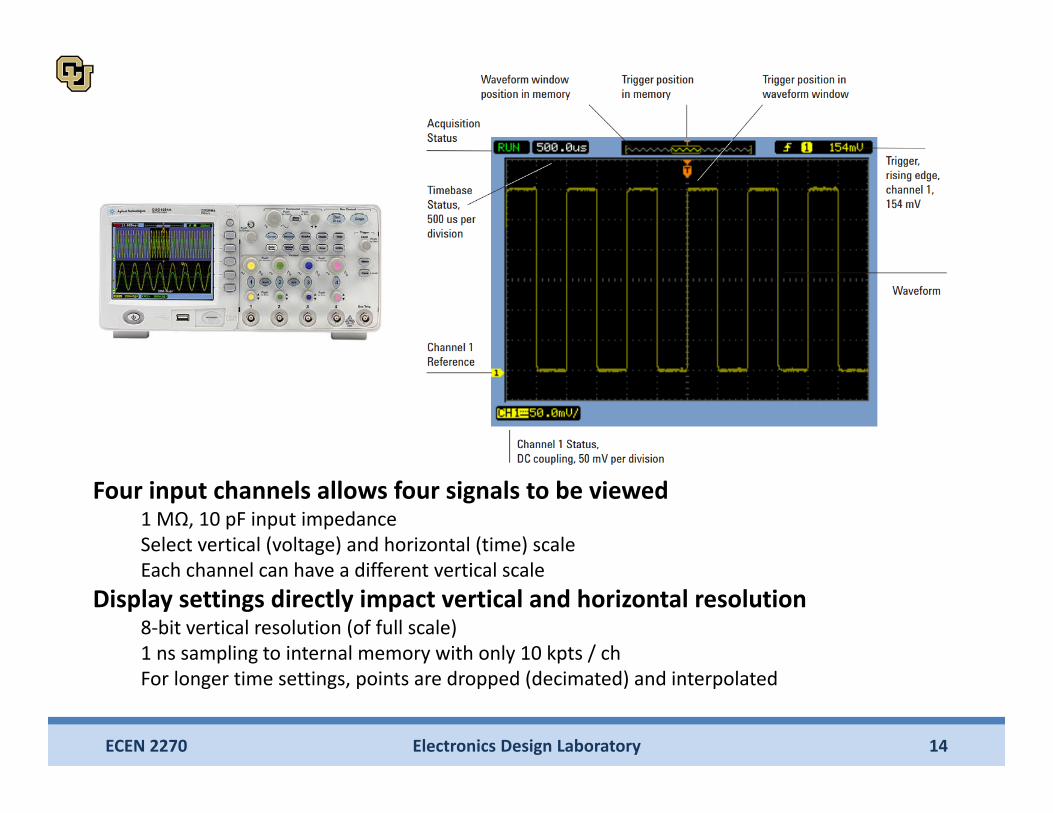
Four input channels allows four signals to be viewed1 MΩ, 10 pF input impedanceSelect vertical (voltage) and horizontal (time) scaleEach channel can have a different vertical scale
Display settings directly impact vertical and horizontal resolution8‐bit vertical resolution (of full scale)1 ns sampling to internal memory with only 10 kpts / chFor longer time settings, points are dropped (decimated) and interpolated
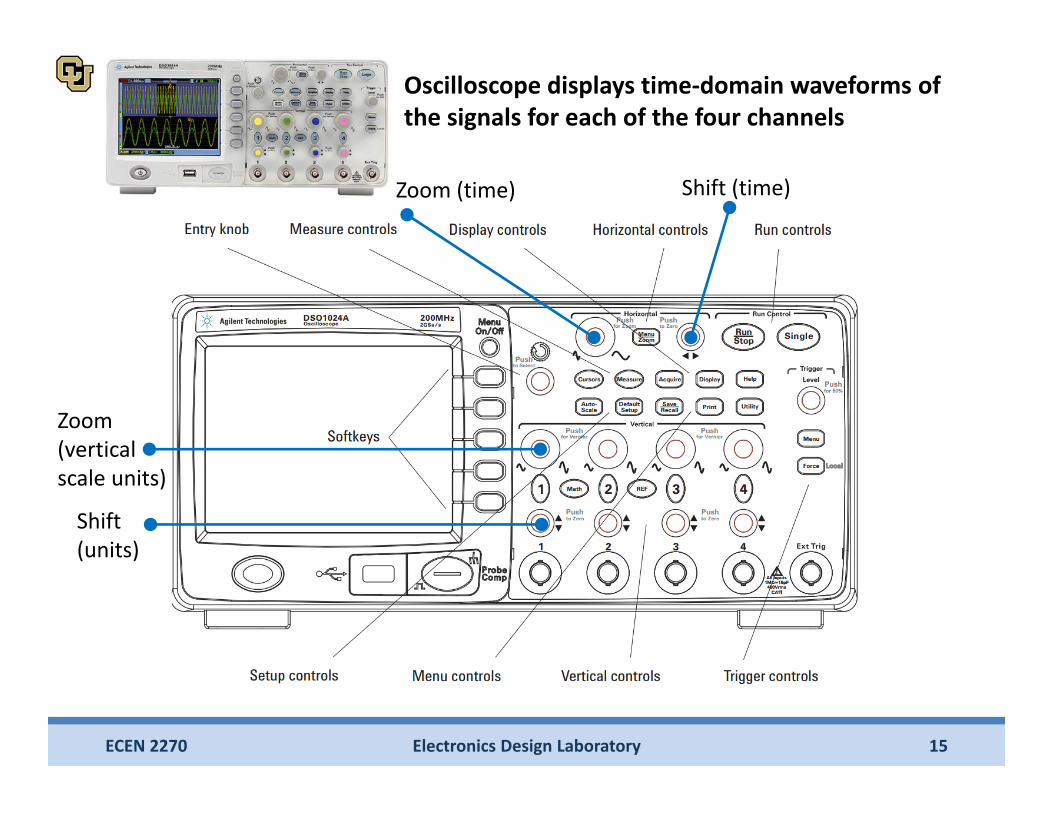
Electronics Design Laboratory 15ECEN 2270
Oscilloscope displays time‐domain waveforms of the signals for each of the four channels
Zoom (time) Shift (time)
Zoom (vertical scale units)
Shift (units)
Electronics Design Laboratory 16ECEN 2270
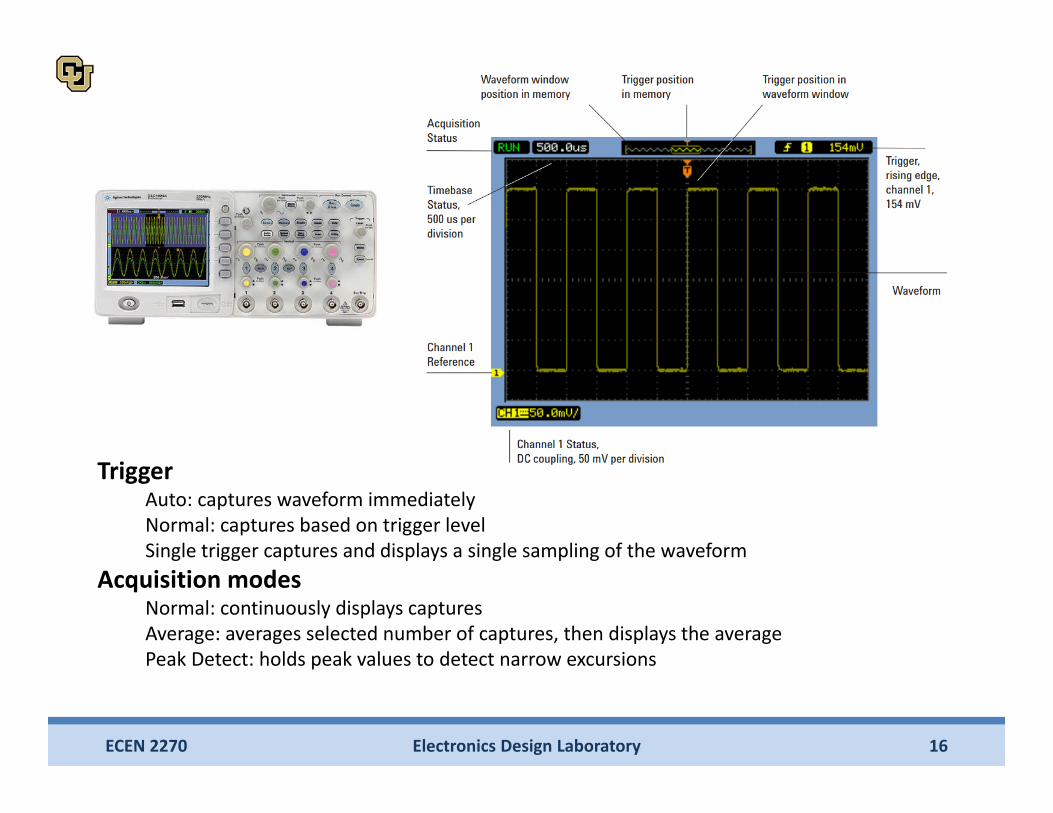
TriggerAuto: captures waveform immediatelyNormal: captures based on trigger level Single trigger captures and displays a single sampling of the waveform
Acquisition modesNormal: continuously displays capturesAverage: averages selected number of captures, then displays the averagePeak Detect: holds peak values to detect narrow excursions
Electronics Design Laboratory 17ECEN 2270
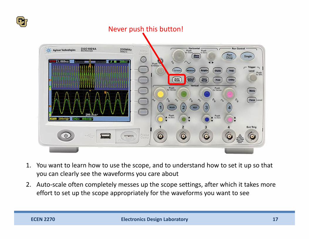
Never push this button!
1. You want to learn how to use the scope, and to understand how to set it up so that you can clearly see the waveforms you care about
2. Auto‐scale often completely messes up the scope settings, after which it takes more effort to set up the scope appropriately for the waveforms you want to see
What to do next• By tomorrow (1st lab period)
– Find team partners– Purchase component and tools kits (if you do not have one)– Browse through lab website: ecee.colorado.edu/ecen2270– Read Lecture 1&2 slides on the lab website– Read through Experiment 1 Part A slides and Lab report
guidelines– Complete Experiment 1 Part A pre‐lab (individually)– Look ahead into next‐week Experiment 1 Part B lecture and lab
slides. Part B pre‐lab is due Tuesday next week (at the latest). In case you finish Part A earlier, you may proceed to Part B before next Tuesday, but you must first complete and turn‐in the Part B pre‐lab assignment
Electronics Design Laboratory 18ECEN 2270
Electronics Design LaboratoryLab 1 Part B
ECEN 2270 19Electronics Design Laboratory
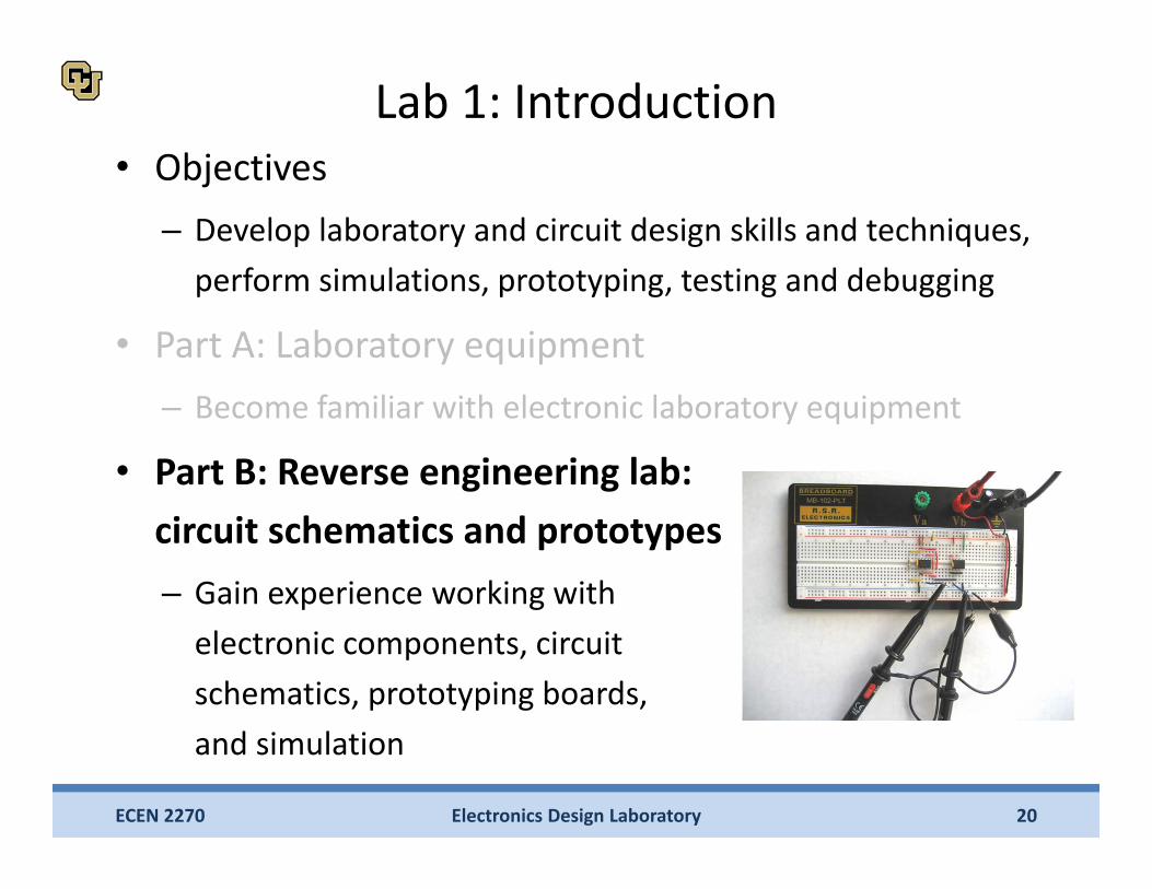
Lab 1: Introduction• Objectives
– Develop laboratory and circuit design skills and techniques, perform simulations, prototyping, testing and debugging
• Part A: Laboratory equipment– Become familiar with electronic laboratory equipment
• Part B: Reverse engineering lab:circuit schematics and prototypes– Gain experience working with electronic components, circuit schematics, prototyping boards, and simulation
Electronics Design Laboratory 20ECEN 2270
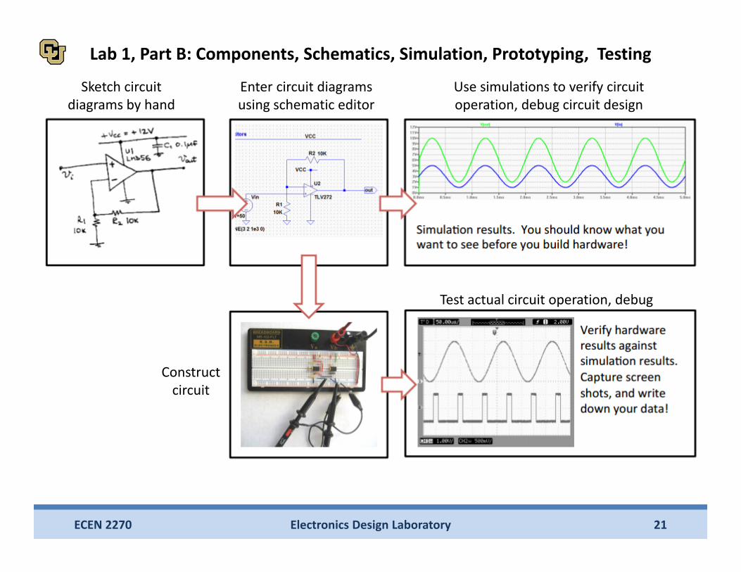
Lab 1, Part B: Components, Schematics, Simulation, Prototyping, Testing
Electronics Design Laboratory 21ECEN 2270
Sketch circuit diagrams by hand
Enter circuit diagrams using schematic editor
Use simulations to verify circuit operation, debug circuit design
Construct circuit
Test actual circuit operation, debug
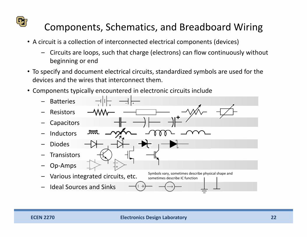
Components, Schematics, and Breadboard Wiring
Electronics Design Laboratory 22ECEN 2270
• A circuit is a collection of interconnected electrical components (devices) – Circuits are loops, such that charge (electrons) can flow continuously without
beginning or end• To specify and document electrical circuits, standardized symbols are used for the devices and the wires that interconnect them.
• Components typically encountered in electronic circuits include – Batteries– Resistors– Capacitors– Inductors– Diodes– Transistors– Op‐Amps– Various integrated circuits, etc. – Ideal Sources and Sinks
Symbols vary, sometimes describe physical shape and sometimes describe IC function
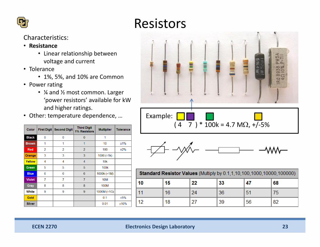
Resistors
Electronics Design Laboratory 23ECEN 2270
Characteristics:• Resistance
• Linear relationship between voltage and current
• Tolerance• 1%, 5%, and 10% are Common
• Power rating• ¼ and ½ most common. Larger ‘power resistors’ available for kW and higher ratings.
• Other: temperature dependence, … Example: ( 4 7 ) * 100k = 4.7 M, +/‐5%
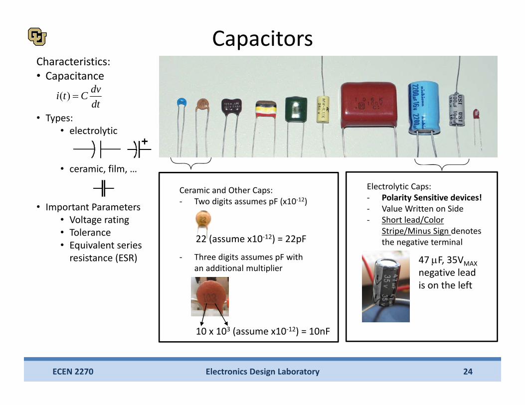
Characteristics:• Capacitance
• Types:• electrolytic
• ceramic, film, …
• Important Parameters• Voltage rating• Tolerance• Equivalent series resistance (ESR)
Ceramic and Other Caps:‐ Two digits assumes pF (x10‐12)
‐ Three digits assumes pF with an additional multiplier
Capacitors
Electronics Design Laboratory 24ECEN 2270
47 F, 35VMAXnegative lead is on the left
22 (assume x10‐12) = 22pF
Electrolytic Caps:‐ Polarity Sensitive devices!‐ Value Written on Side‐ Short lead/Color
Stripe/Minus Sign denotes the negative terminal
10 x 103 (assume x10‐12) = 10nF
dtdvCti )(
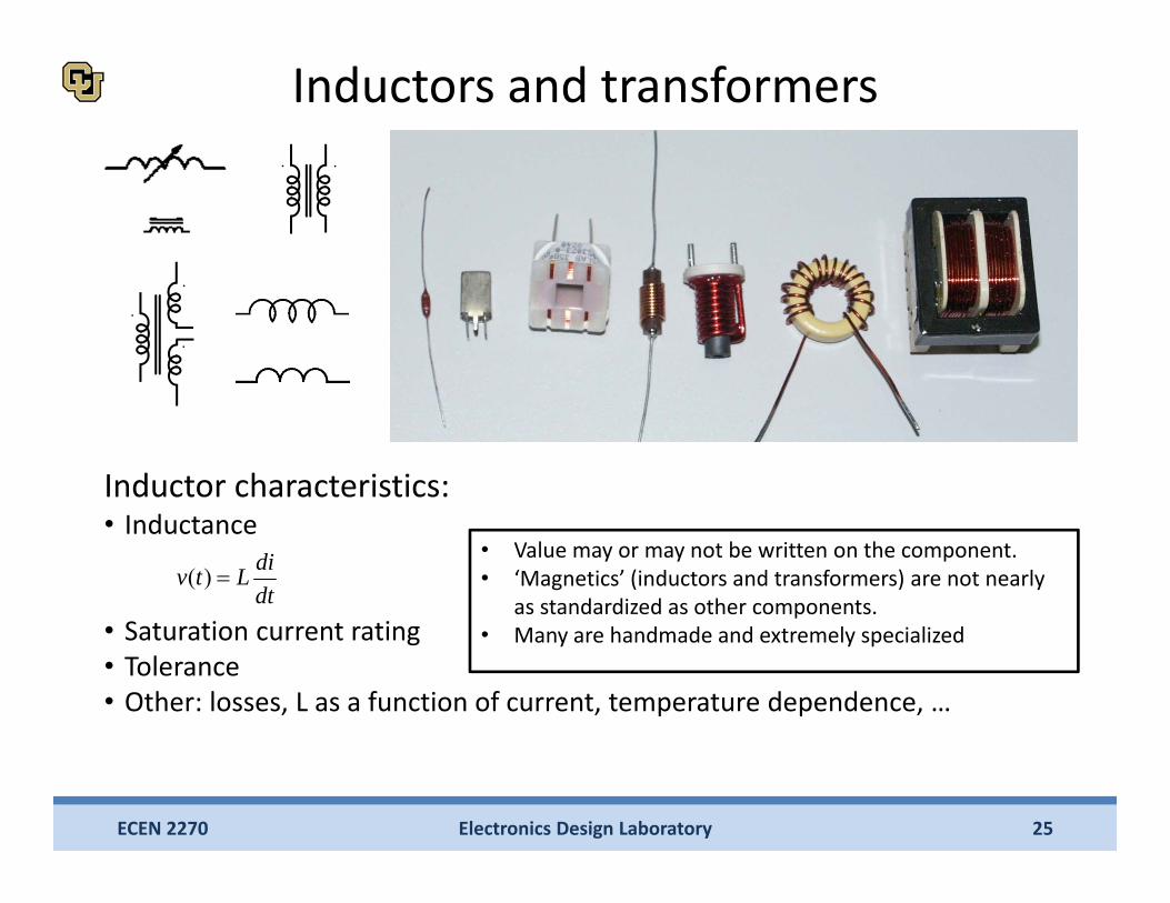
Inductors and transformers
Electronics Design Laboratory 25ECEN 2270
Inductor characteristics:• Inductance
• Saturation current rating• Tolerance• Other: losses, L as a function of current, temperature dependence, …
• •
•
•
•• Value may or may not be written on the component. • ‘Magnetics’ (inductors and transformers) are not nearly
as standardized as other components.• Many are handmade and extremely specialized
dtdiLtv )(
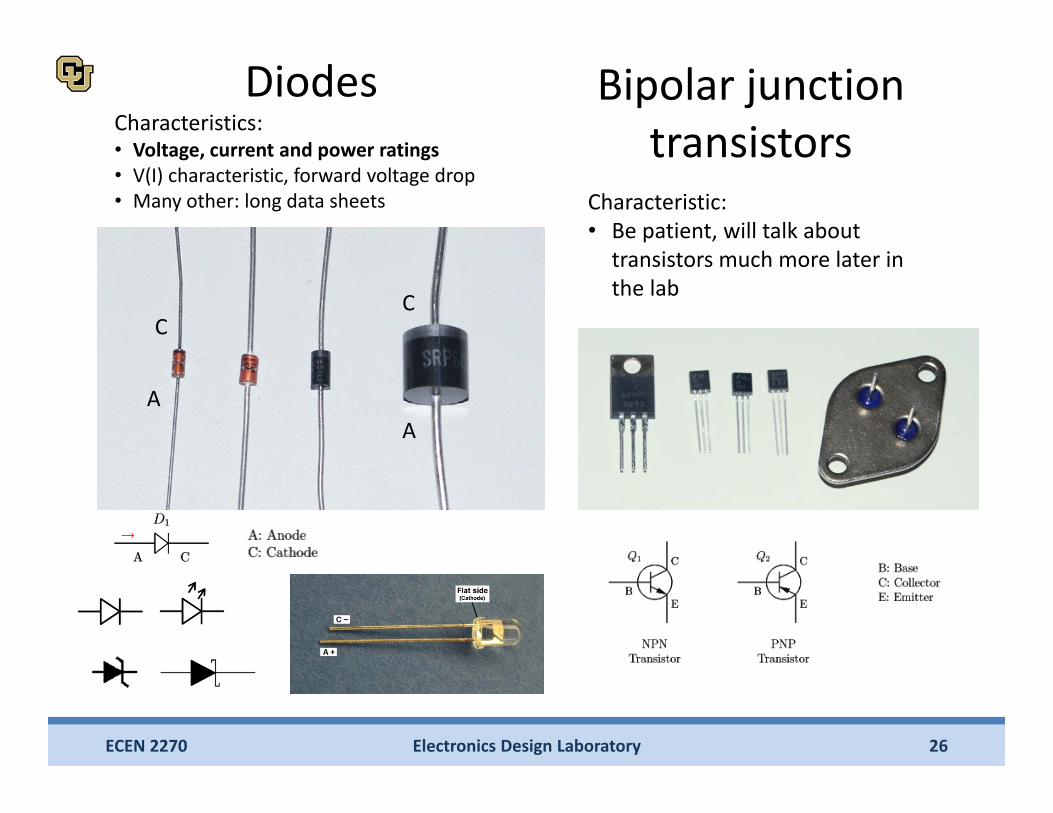
A
CC
A
Diodes
Electronics Design Laboratory 26ECEN 2270
Characteristics:• Voltage, current and power ratings• V(I) characteristic, forward voltage drop• Many other: long data sheets
Bipolar junction transistors
Characteristic: • Be patient, will talk about
transistors much more later in the lab
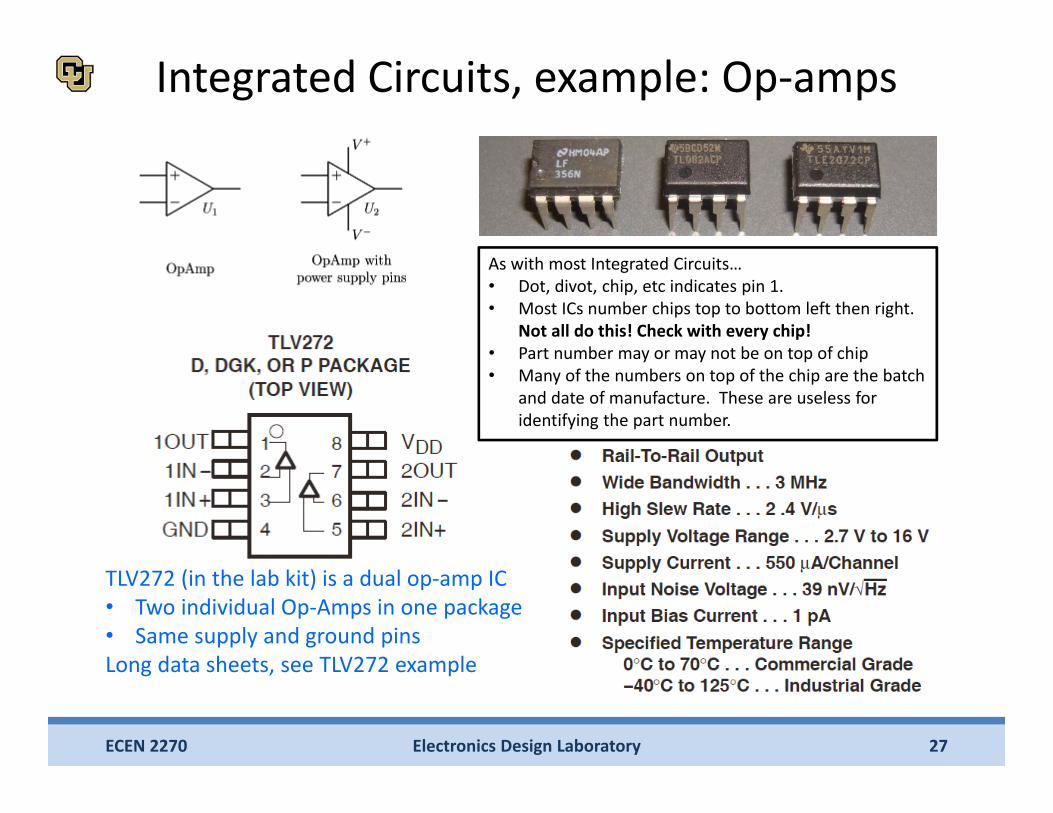
Integrated Circuits, example: Op‐amps
Electronics Design Laboratory 27ECEN 2270
TLV272 (in the lab kit) is a dual op‐amp IC• Two individual Op‐Amps in one package• Same supply and ground pinsLong data sheets, see TLV272 example
As with most Integrated Circuits…• Dot, divot, chip, etc indicates pin 1.• Most ICs number chips top to bottom left then right.
Not all do this! Check with every chip!• Part number may or may not be on top of chip• Many of the numbers on top of the chip are the batch
and date of manufacture. These are useless for identifying the part number.
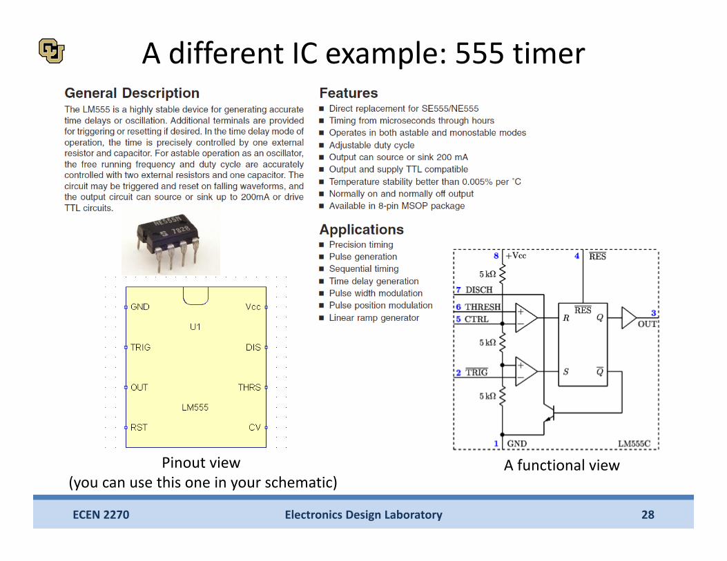
A different IC example: 555 timer
Electronics Design Laboratory 28ECEN 2270
Pinout view (you can use this one in your schematic)
A functional view
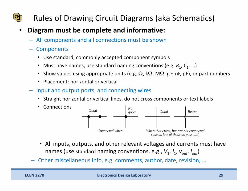
Rules of Drawing Circuit Diagrams (aka Schematics)• Diagram must be complete and informative:
– All components and all connections must be shown– Components
• Use standard, commonly accepted component symbols• Must have names, use standard naming conventions (e.g. R1, C1, …)• Show values using appropriate units (e.g. , k, M, F, nF, pF), or part numbers• Placement: horizontal or vertical
– Input and output ports, and connecting wires• Straight horizontal or vertical lines, do not cross components or text labels• Connections
Electronics Design Laboratory 29ECEN 2270
• All inputs, outputs, and other relevant voltages and currents must have names (use standard naming conventions, e.g., V1, I1, vout, iout)
– Other miscellaneous info, e.g. comments, author, date, revision, …
Wires that cross, but are not connected(use as few of these as possible)
Good BetterNotgoodGood
Connected wires
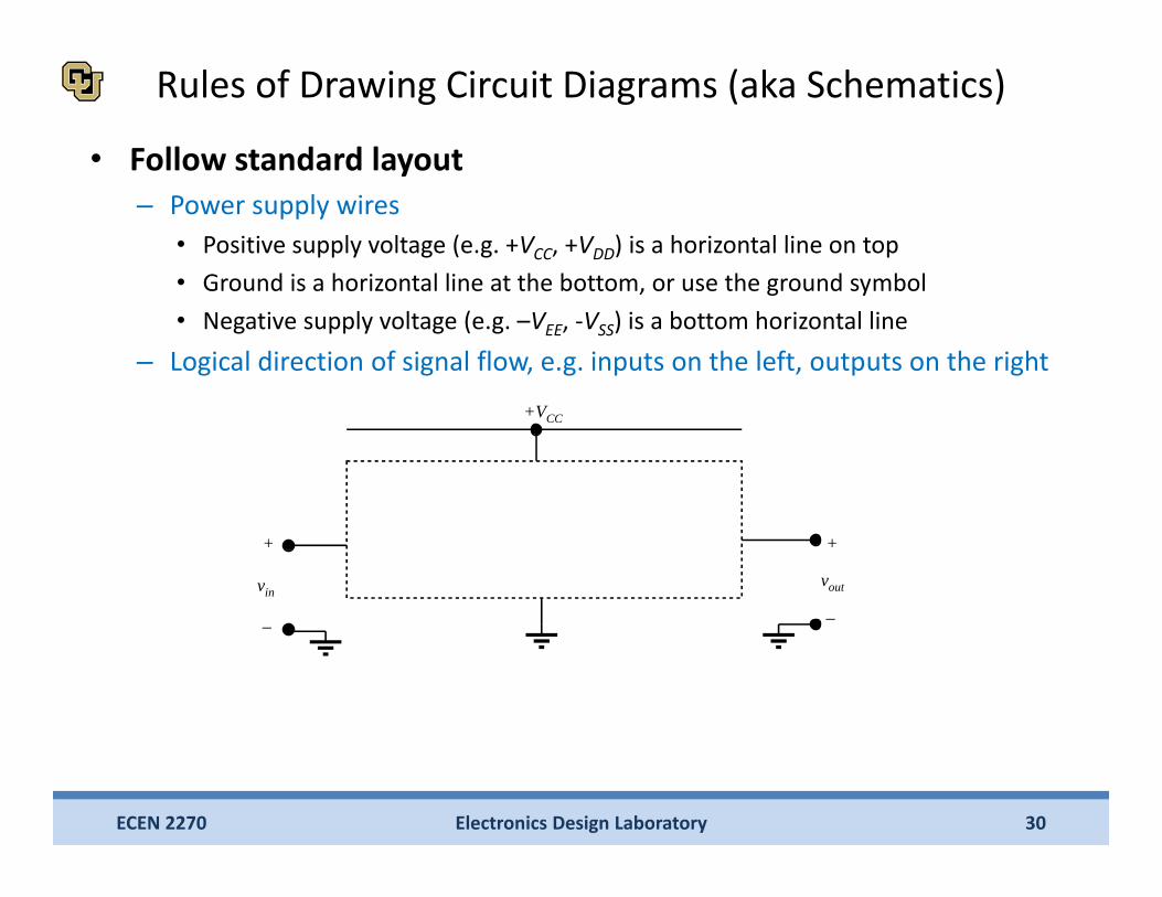
Rules of Drawing Circuit Diagrams (aka Schematics)
• Follow standard layout– Power supply wires
• Positive supply voltage (e.g. +VCC, +VDD) is a horizontal line on top• Ground is a horizontal line at the bottom, or use the ground symbol• Negative supply voltage (e.g. –VEE, ‐VSS) is a bottom horizontal line
– Logical direction of signal flow, e.g. inputs on the left, outputs on the right
Electronics Design Laboratory 30ECEN 2270
+VCC
+
_
vinvout
+
_
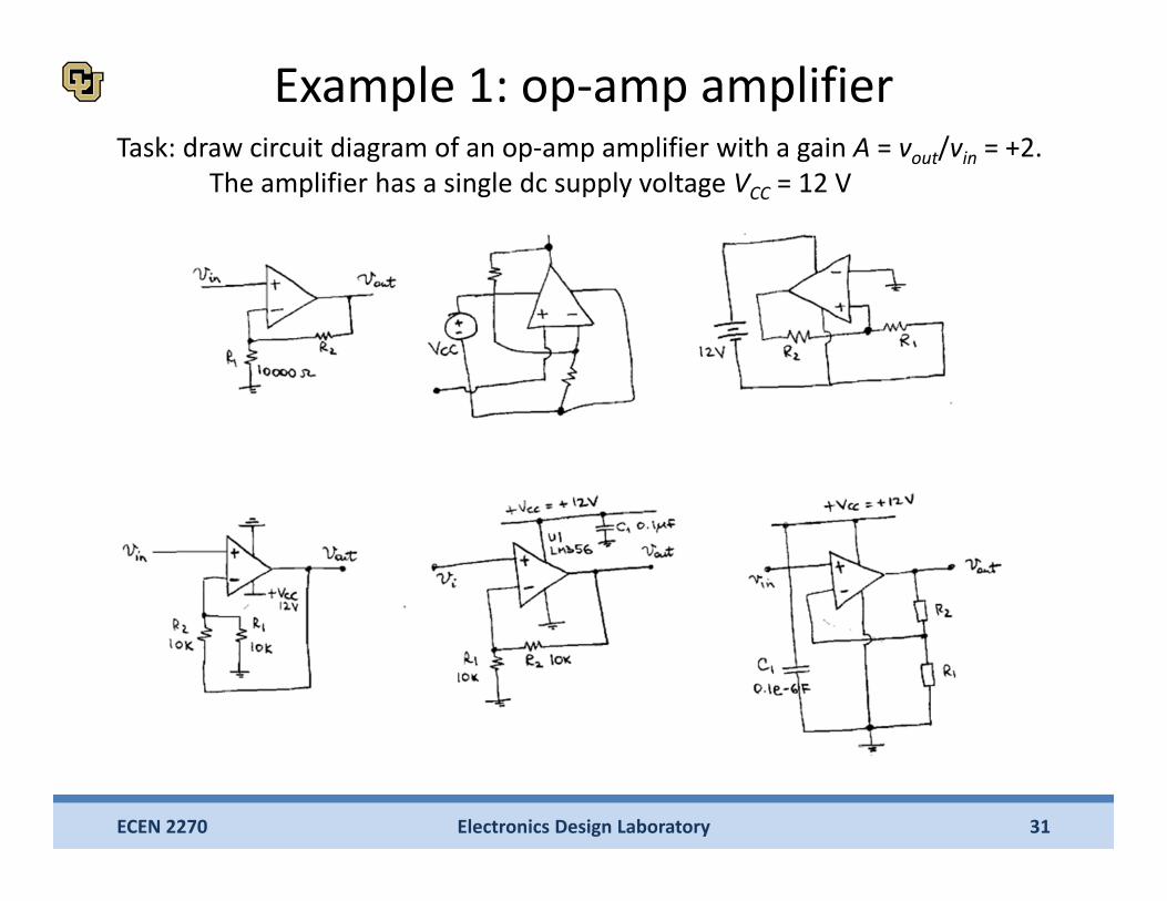
Example 1: op‐amp amplifierTask: draw circuit diagram of an op‐amp amplifier with a gain A = vout/vin = +2.
The amplifier has a single dc supply voltage VCC = 12 V
Electronics Design Laboratory 31ECEN 2270
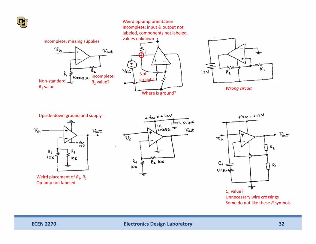
Electronics Design Laboratory 32ECEN 2270
Incomplete: missing supplies
Incomplete: R2 value?Non‐standard
R1 value
Weird op‐amp orientationIncomplete: input & output not labeled, components not labeled, values unknown
Where is ground?
Not straight
?
Upside‐down ground and supply
Weird placement of R1, R2Op‐amp not labeled
C1 value?Unnecessary wire crossingsSome do not like these R symbols
Wrong circuit
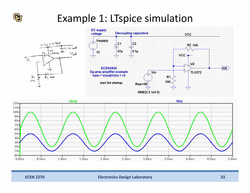
Example 1: LTspice simulation
Electronics Design Laboratory 33ECEN 2270
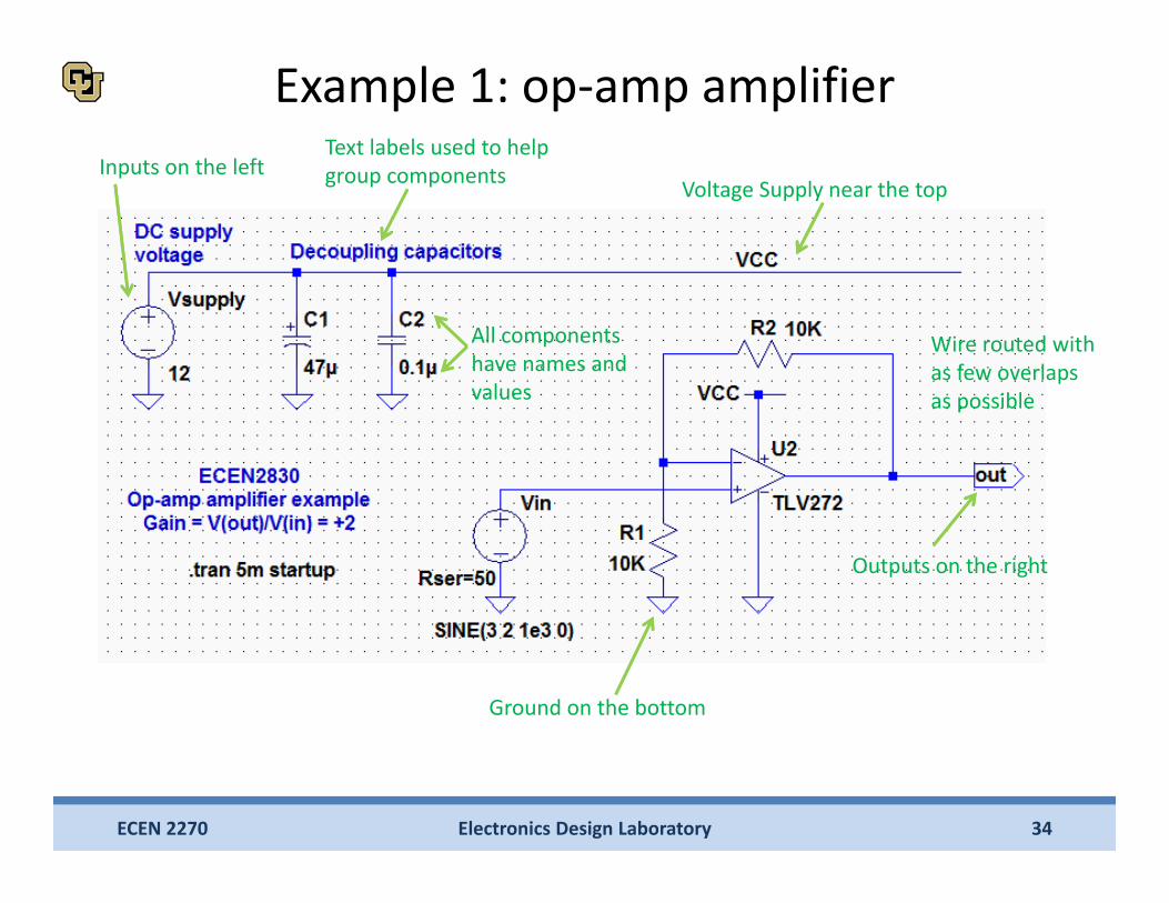
Example 1: op‐amp amplifier
Electronics Design Laboratory 34ECEN 2270
Inputs on the left
Outputs on the right
Ground on the bottom
Voltage Supply near the top
Text labels used to help group components
All components have names and values
Wire routed with as few overlaps as possible
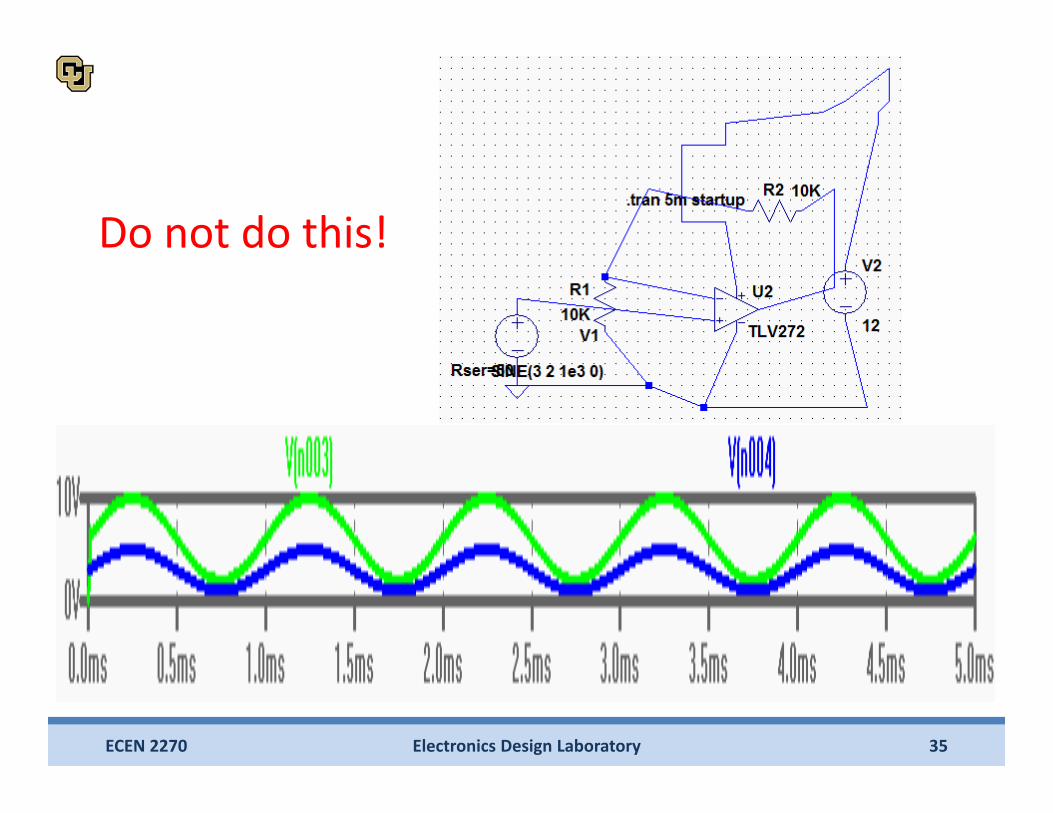
Do not do this!
Electronics Design Laboratory 35ECEN 2270
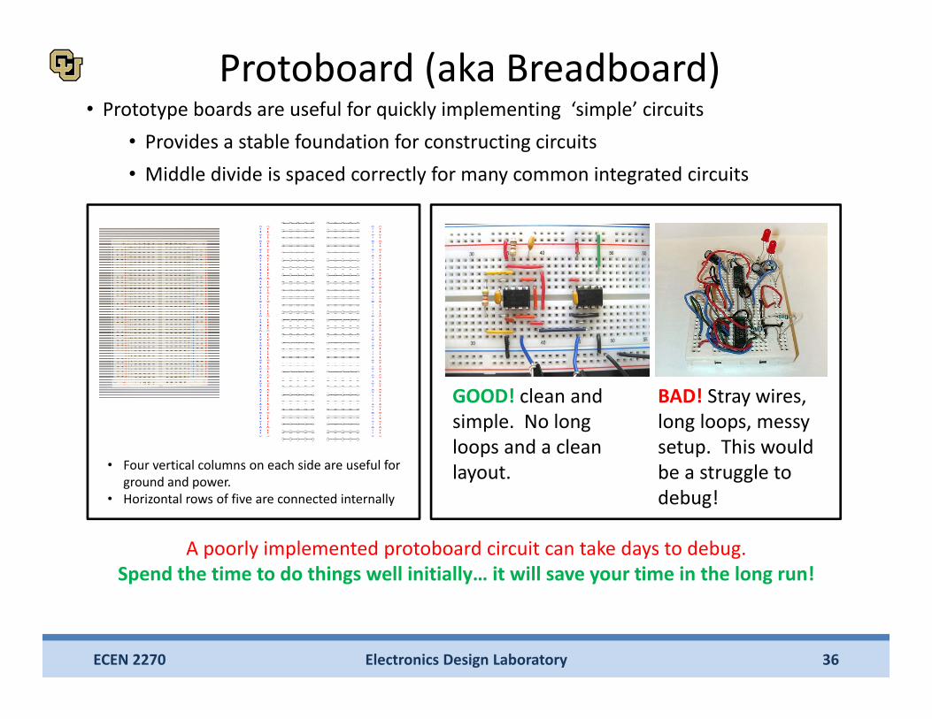
Protoboard (aka Breadboard)
Electronics Design Laboratory 36ECEN 2270
• Prototype boards are useful for quickly implementing ‘simple’ circuits• Provides a stable foundation for constructing circuits• Middle divide is spaced correctly for many common integrated circuits
• Four vertical columns on each side are useful for ground and power.
• Horizontal rows of five are connected internally
GOOD! clean and simple. No long loops and a clean layout.
BAD! Stray wires, long loops, messy setup. This would be a struggle to debug!
A poorly implemented protoboard circuit can take days to debug.Spend the time to do things well initially… it will save your time in the long run!
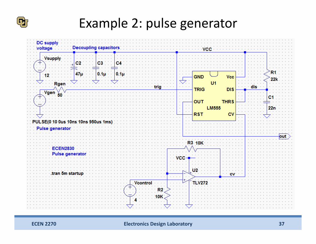
Example 2: pulse generator
Electronics Design Laboratory 37ECEN 2270
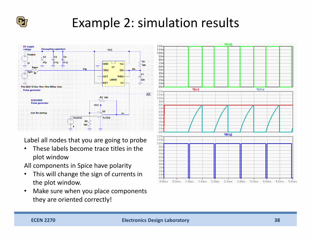
Example 2: simulation results
Electronics Design Laboratory 38ECEN 2270
Label all nodes that you are going to probe• These labels become trace titles in the
plot windowAll components in Spice have polarity• This will change the sign of currents in
the plot window. • Make sure when you place components
they are oriented correctly!