Embed Size (px)
Citation preview
ELEN 468 Lecture 11 1
ELEN 468Advanced Logic Design
Lecture 11Switch Level Models
ELEN 468 Lecture 11 2
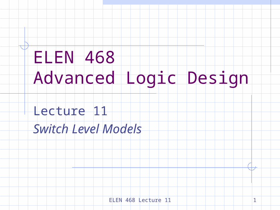
MOS Transistor Technology
p substraten well
n n p p
source source
drain
gate gate
g
d
s
s
d
g
ELEN 468 Lecture 11 3
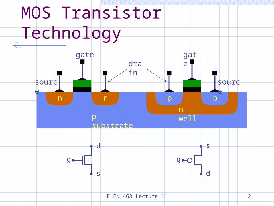
Switch Level Models
nmos control
Input 0 1 x z
0 z 0 L L
1 z 1 H H
x z x x x
z z z z z
pmos control
Input 0 1 x z
0 0 z L L
1 1 z H H
x x z x x
z z z z z
L => 0 or z, H => 1 or z
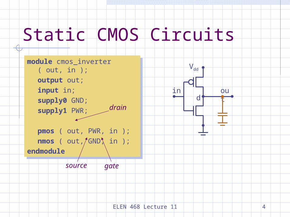
ELEN 468 Lecture 11 4
Static CMOS Circuits
module cmos_inverter ( out, in );output out;input in;supply0 GND;supply1 PWR;
pmos ( out, PWR, in );nmos ( out, GND, in );
endmodule
module cmos_inverter ( out, in );output out;input in;supply0 GND;supply1 PWR;
pmos ( out, PWR, in );nmos ( out, GND, in );
endmodule
din ou
t
Vdd
drain
source gate
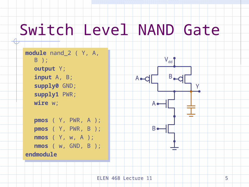
ELEN 468 Lecture 11 5
Switch Level NAND Gatemodule nand_2 ( Y, A,
B );output Y;input A, B;supply0 GND;supply1 PWR;wire w;
pmos ( Y, PWR, A );pmos ( Y, PWR, B );nmos ( Y, w, A );nmos ( w, GND, B );
endmodule
module nand_2 ( Y, A, B );output Y;input A, B;supply0 GND;supply1 PWR;wire w;
pmos ( Y, PWR, A );pmos ( Y, PWR, B );nmos ( Y, w, A );nmos ( w, GND, B );
endmodule
Y
Vdd
A
A
B
B
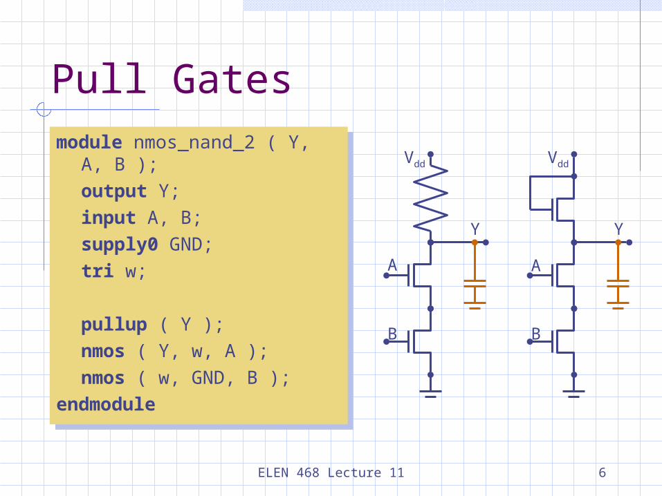
ELEN 468 Lecture 11 6
Pull Gates
module nmos_nand_2 ( Y, A, B );output Y;input A, B;supply0 GND;tri w;
pullup ( Y );nmos ( Y, w, A );nmos ( w, GND, B );
endmodule
module nmos_nand_2 ( Y, A, B );output Y;input A, B;supply0 GND;tri w;
pullup ( Y );nmos ( Y, w, A );nmos ( w, GND, B );
endmodule
Y
Vdd
A
B
Y
Vdd
A
B
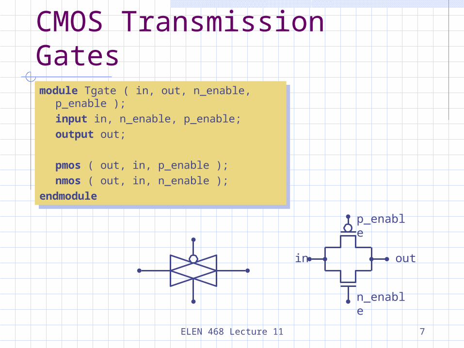
ELEN 468 Lecture 11 7
CMOS Transmission Gatesmodule Tgate ( in, out, n_enable,
p_enable );input in, n_enable, p_enable;output out;
pmos ( out, in, p_enable );nmos ( out, in, n_enable );
endmodule
module Tgate ( in, out, n_enable, p_enable );input in, n_enable, p_enable;output out;
pmos ( out, in, p_enable );nmos ( out, in, n_enable );
endmodule
in out
p_enable
n_enable
ELEN 468 Lecture 11 8
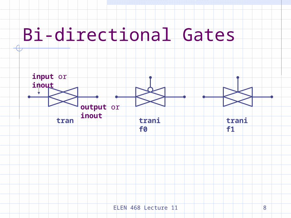
Bi-directional Gates
tran tranif0
tranif1
input or inout
output or inout
ELEN 468 Lecture 11 9
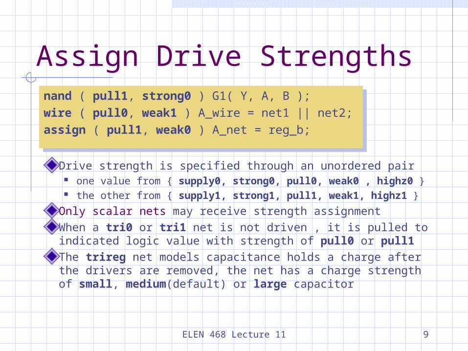
Assign Drive Strengthsnand ( pull1, strong0 ) G1( Y, A, B );wire ( pull0, weak1 ) A_wire = net1 || net2;assign ( pull1, weak0 ) A_net = reg_b;
nand ( pull1, strong0 ) G1( Y, A, B );wire ( pull0, weak1 ) A_wire = net1 || net2;assign ( pull1, weak0 ) A_net = reg_b;
Drive strength is specified through an unordered pair one value from { supply0, strong0, pull0, weak0 , highz0 } the other from { supply1, strong1, pull1, weak1, highz1 }
Only scalar nets may receive strength assignmentWhen a tri0 or tri1 net is not driven , it is pulled to indicated logic value with strength of pull0 or pull1The trireg net models capacitance holds a charge after the drivers are removed, the net has a charge strength of small, medium(default) or large capacitor
ELEN 468 Lecture 11 10
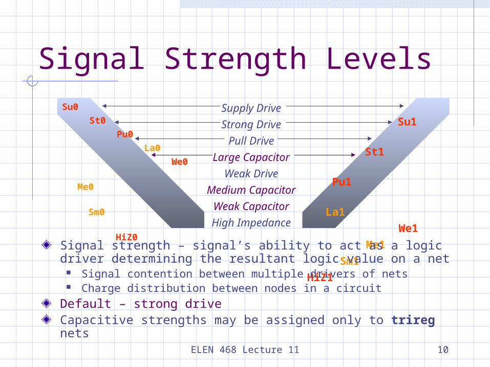
Signal Strength LevelsSu0
St0
Pu0
La0
We0
Me0
Sm0
HiZ0
Su1
St1
Pu1
La1
We1
Me1
Sm1
HiZ1
Supply Drive
Strong Drive
Pull Drive
Large Capacitor
Weak Drive
Medium Capacitor
Weak Capacitor
High ImpedanceSignal strength – signal’s ability to act as a logic driver determining the resultant logic value on a net
Signal contention between multiple drivers of nets Charge distribution between nodes in a circuit
Default – strong driveCapacitive strengths may be assigned only to trireg nets
ELEN 468 Lecture 11 11
StL
PuH
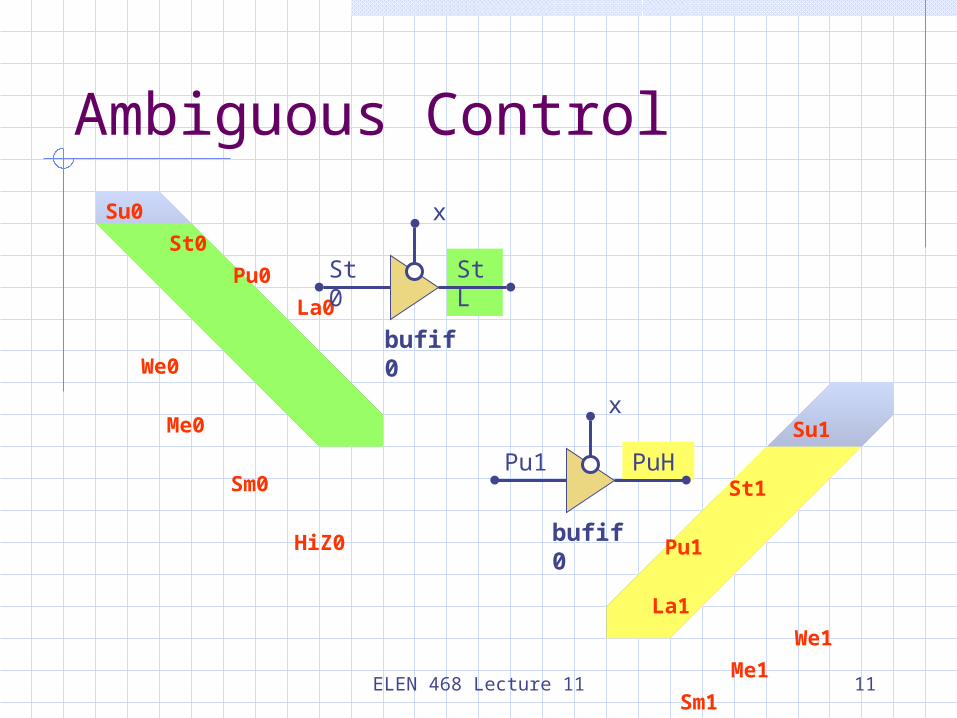
Ambiguous ControlSu0
St0
Pu0
La0
We0
Me0
Sm0
HiZ0
Su1
St1
Pu1
La1
We1
Me1
Sm1
HiZ1
x
bufif0
St0
x
bufif0
Pu1
ELEN 468 Lecture 11 12
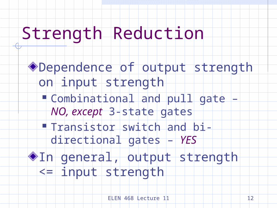
Strength Reduction
Dependence of output strength on input strength Combinational and pull gate – NO,
except 3-state gates Transistor switch and bi-directional
gates – YES
In general, output strength <= input strength
ELEN 468 Lecture 11 13
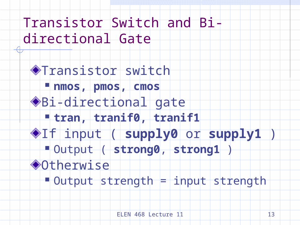
Transistor Switch and Bi-directional Gate
Transistor switch nmos, pmos, cmos
Bi-directional gate tran, tranif0, tranif1
If input ( supply0 or supply1 ) Output ( strong0, strong1 )
Otherwise Output strength = input strength
ELEN 468 Lecture 11 14
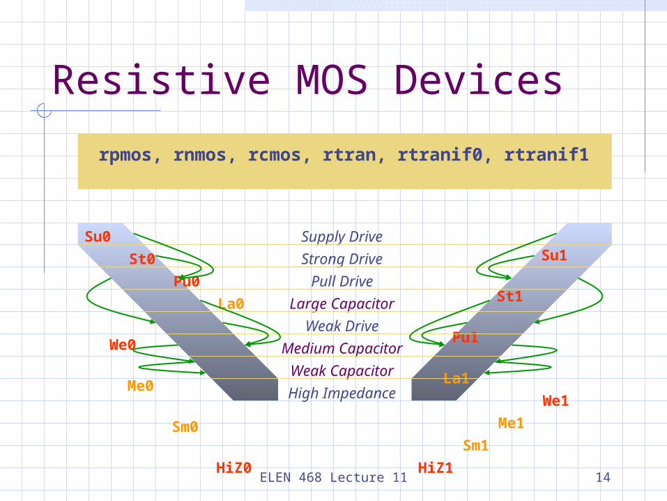
Resistive MOS Devices
rpmos, rnmos, rcmos, rtran, rtranif0, rtranif1
Su0
St0
Pu0
La0
We0
Me0
Sm0
HiZ0
Su1
St1
Pu1
La1
We1
Me1
Sm1
HiZ1
Supply Drive
Strong Drive
Pull Drive
Large Capacitor
Weak Drive
Medium Capacitor
Weak Capacitor
High Impedance
ELEN 468 Lecture 11 15
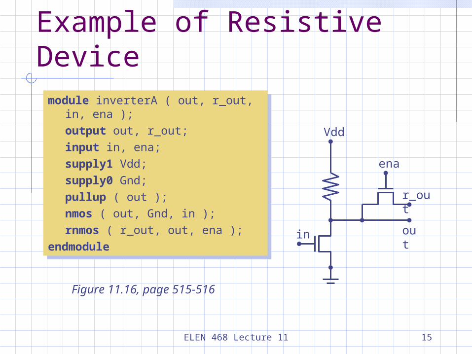
Example of Resistive Device
module inverterA ( out, r_out, in, ena );output out, r_out;input in, ena;supply1 Vdd;supply0 Gnd;pullup ( out );nmos ( out, Gnd, in );rnmos ( r_out, out, ena );
endmodule
module inverterA ( out, r_out, in, ena );output out, r_out;input in, ena;supply1 Vdd;supply0 Gnd;pullup ( out );nmos ( out, Gnd, in );rnmos ( r_out, out, ena );
endmodule
in out
r_out
ena
Vdd
Figure 11.16, page 515-516
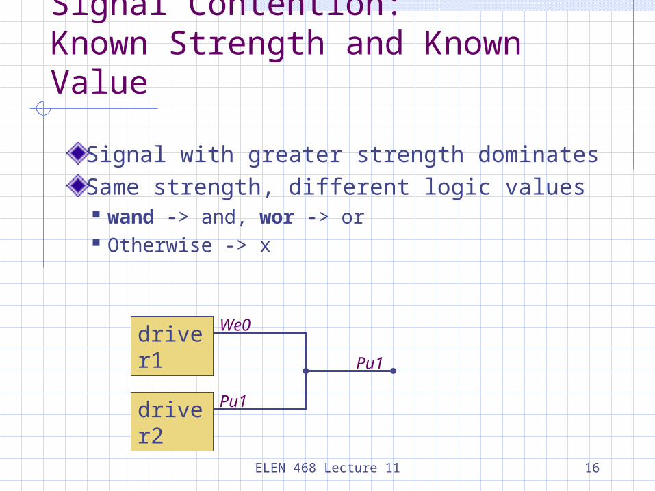
ELEN 468 Lecture 11 16
Signal Contention: Known Strength and Known Value
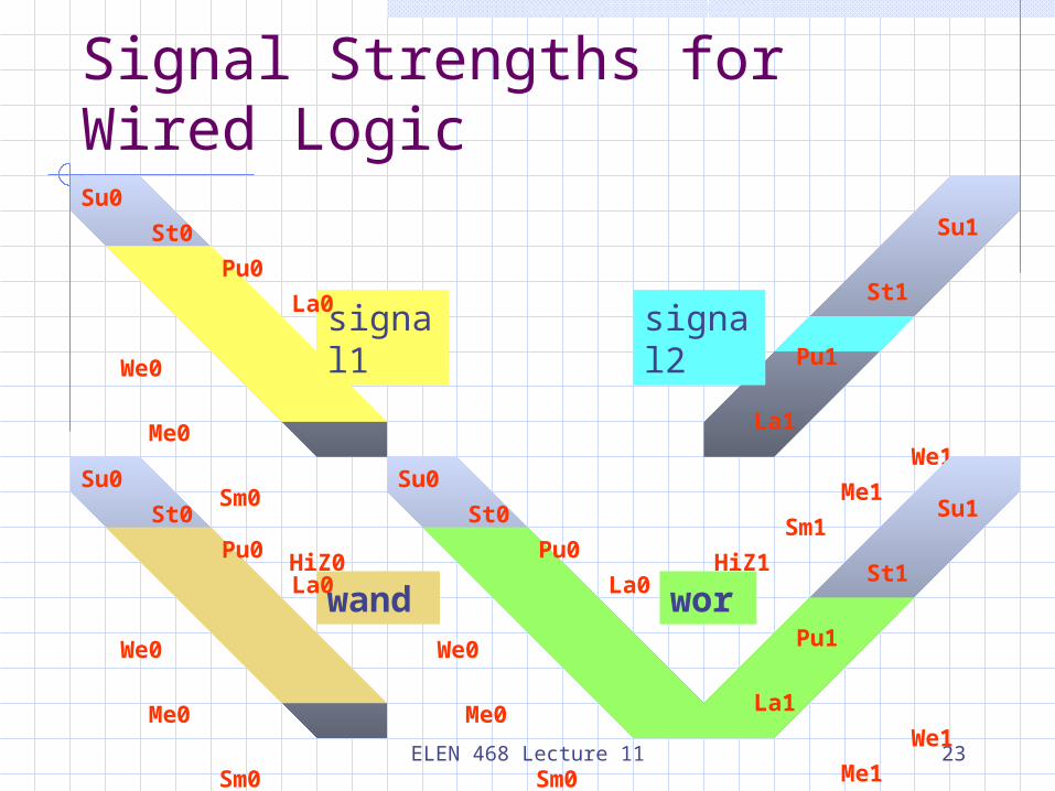
Signal with greater strength dominatesSame strength, different logic values wand -> and, wor -> or Otherwise -> x
driver1
driver2
We0
Pu1
Pu1
ELEN 468 Lecture 11 17
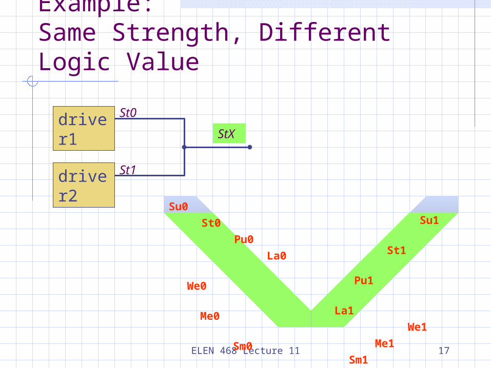
Example: Same Strength, Different Logic Value
Su0
St0
Pu0
La0
We0
Me0
Sm0
HiZ0
Su1
St1
Pu1
La1
We1
Me1
Sm1
HiZ1
driver1
driver2
St0
St1
StX
ELEN 468 Lecture 11 18
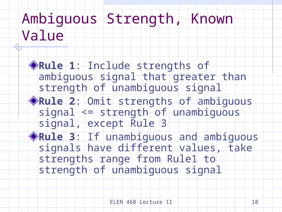
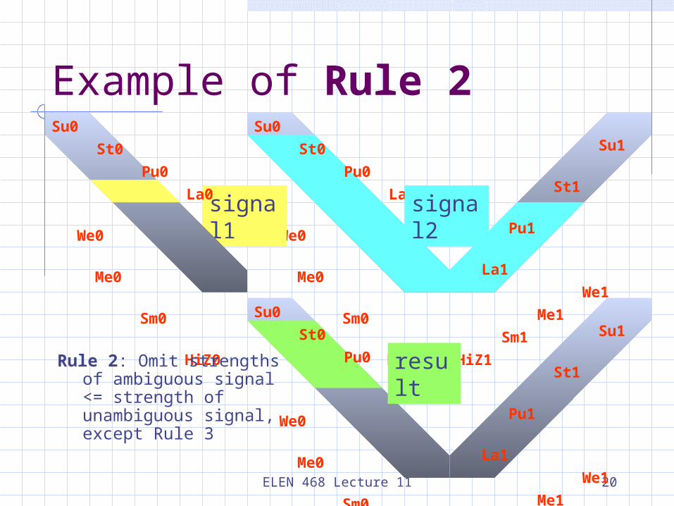
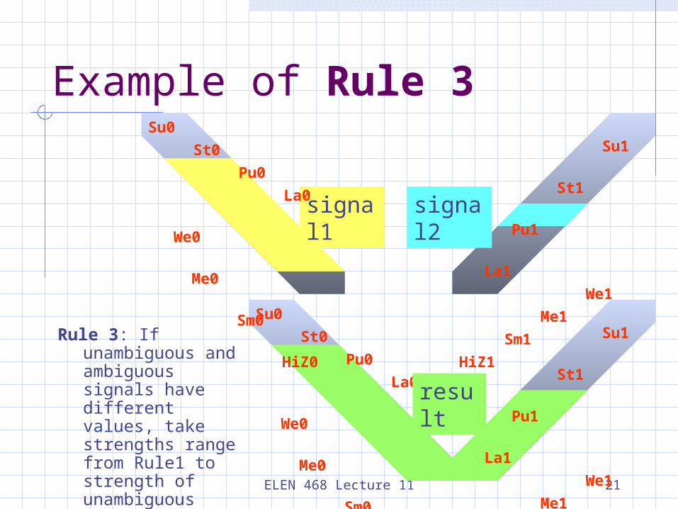
Ambiguous Strength, Known Value
Rule 1: Include strengths of ambiguous signal that greater than strength of unambiguous signalRule 2: Omit strengths of ambiguous signal <= strength of unambiguous signal, except Rule 3Rule 3: If unambiguous and ambiguous signals have different values, take strengths range from Rule1 to strength of unambiguous signal
ELEN 468 Lecture 11 19
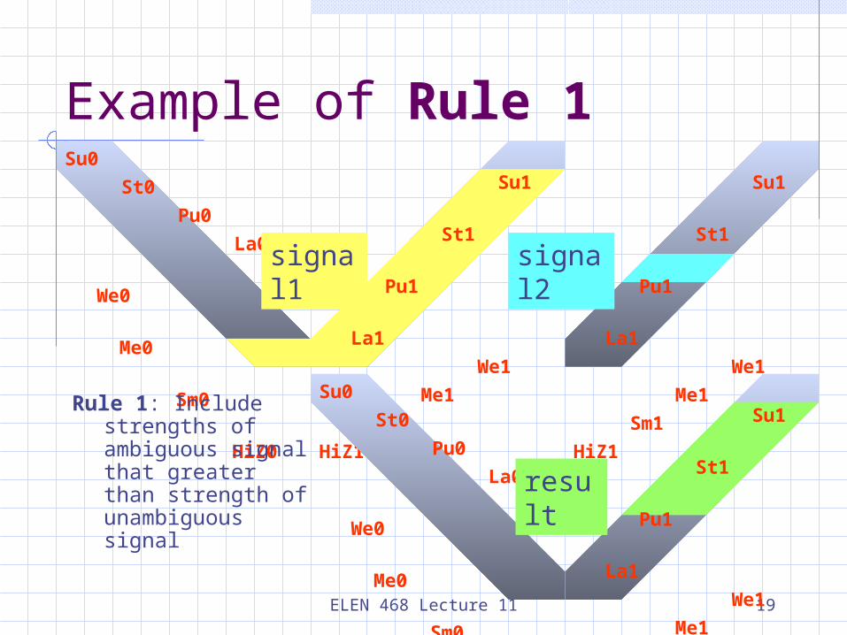
Example of Rule 1
Su1
St1
Pu1
La1
We1
Me1
Sm1
HiZ1
Su1
St1
Pu1
La1
We1
Me1
Sm1
HiZ1
Su0
St0
Pu0
La0
We0
Me0
Sm0
HiZ0
signal1
signal2
Su1
St1
Pu1
La1
We1
Me1
Sm1
HiZ1
Su0
St0
Pu0
La0
We0
Me0
Sm0
HiZ0
result
Rule 1: Include strengths of ambiguous signal that greater than strength of unambiguous signal
ELEN 468 Lecture 11 20
Example of Rule 2
Su1
St1
Pu1
La1
We1
Me1
Sm1
HiZ1
Su0
St0
Pu0
La0
We0
Me0
Sm0
HiZ0
signal1
signal2
Su1
St1
Pu1
La1
We1
Me1
Sm1
HiZ1
Su0
St0
Pu0
La0
We0
Me0
Sm0
HiZ0
result
Su0
St0
Pu0
La0
We0
Me0
Sm0
HiZ0
Rule 2: Omit strengths of ambiguous signal <= strength of unambiguous signal, except Rule 3
ELEN 468 Lecture 11 21
Example of Rule 3
Su1
St1
Pu1
La1
We1
Me1
Sm1
HiZ1
signal2
Su1
St1
Pu1
La1
We1
Me1
Sm1
HiZ1
Su0
St0
Pu0
La0
We0
Me0
Sm0
HiZ0
result
signal1
Su0
St0
Pu0
La0
We0
Me0
Sm0
HiZ0
Rule 3: If unambiguous and ambiguous signals have different values, take strengths range from Rule1 to strength of unambiguous signal
ELEN 468 Lecture 11 22
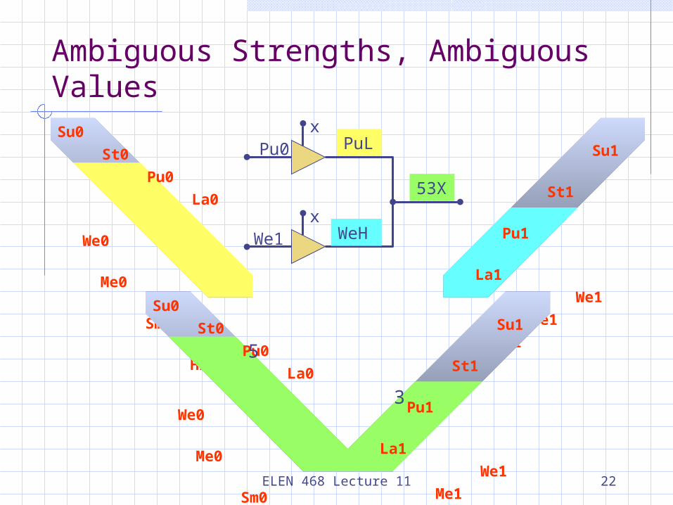
Ambiguous Strengths, Ambiguous ValuesSu0
St0
Pu0
La0
We0
Me0
Sm0
HiZ0
Su1
St1
Pu1
La1
We1
Me1
Sm1
HiZ1
x
x
Pu0
We1 WeH
PuL
53X
Su0
St0
Pu0
La0
We0
Me0
Sm0
HiZ0
Su1
St1
Pu1
La1
We1
Me1
Sm1
HiZ1
5
3
ELEN 468 Lecture 11 23
Signal Strengths for Wired Logic
Su1
St1
Pu1
La1
We1
Me1
Sm1
HiZ1
signal2
Su1
St1
Pu1
La1
We1
Me1
Sm1
HiZ1
Su0
St0
Pu0
La0
We0
Me0
Sm0
HiZ0
wor
signal1
Su0
St0
Pu0
La0
We0
Me0
Sm0
HiZ0
wand
Su0
St0
Pu0
La0
We0
Me0
Sm0
HiZ0
ELEN 468 Lecture 11 24
Exercise Exercise 22
ELEN 468 Lecture 11 25
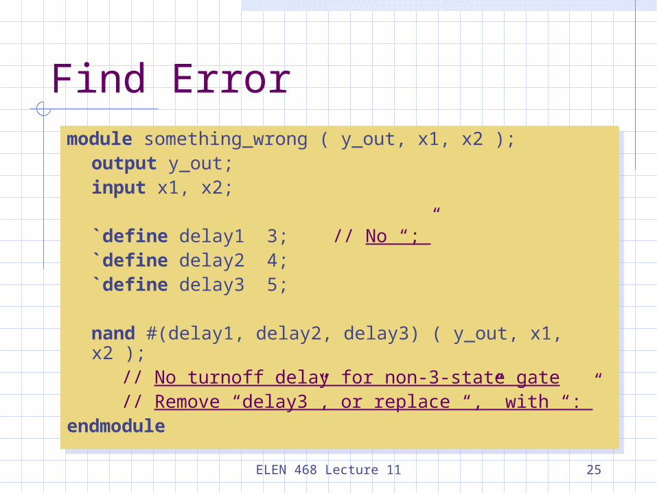
Find Errormodule something_wrong ( y_out, x1, x2 );
output y_out;input x1, x2;
`define delay1 3; // No “;”`define delay2 4;`define delay3 5;
nand #(delay1, delay2, delay3) ( y_out, x1, x2 ); // No turnoff delay for non-3-state gate // Remove “delay3”, or replace “,” with “:”endmodule
module something_wrong ( y_out, x1, x2 );output y_out;input x1, x2;
`define delay1 3; // No “;”`define delay2 4;`define delay3 5;
nand #(delay1, delay2, delay3) ( y_out, x1, x2 ); // No turnoff delay for non-3-state gate // Remove “delay3”, or replace “,” with “:”endmodule
ELEN 468 Lecture 11 26
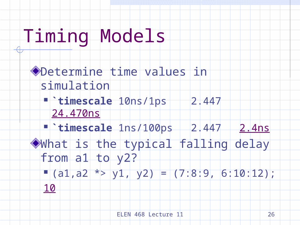
Timing Models
Determine time values in simulation `timescale 10ns/1ps 2.447 24.470ns `timescale 1ns/100ps 2.447 2.4ns
What is the typical falling delay from a1 to y2? (a1,a2 *> y1, y2) = (7:8:9, 6:10:12);10
ELEN 468 Lecture 11 27
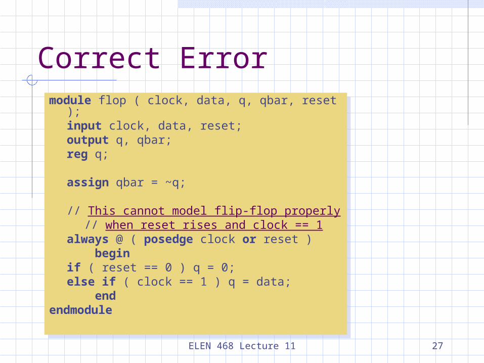
Correct Errormodule flop ( clock, data, q, qbar, reset );
input clock, data, reset;output q, qbar;reg q;
assign qbar = ~q;
// This cannot model flip-flop properly // when reset rises and clock == 1
always @ ( posedge clock or reset ) begin
if ( reset == 0 ) q = 0;else if ( clock == 1 ) q = data;
endendmodule
module flop ( clock, data, q, qbar, reset );input clock, data, reset;output q, qbar;reg q;
assign qbar = ~q;
// This cannot model flip-flop properly // when reset rises and clock == 1
always @ ( posedge clock or reset ) begin
if ( reset == 0 ) q = 0;else if ( clock == 1 ) q = data;
endendmodule
ELEN 468 Lecture 11 28
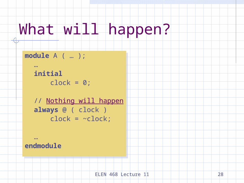
What will happen?
module A ( … );…initial clock = 0;
// Nothing will happenalways @ ( clock ) clock = ~clock;
…endmodule
module A ( … );…initial clock = 0;
// Nothing will happenalways @ ( clock ) clock = ~clock;
…endmodule