Embed Size (px)
Citation preview
Lei JiangSr. Staff Engineer
Thermo Mechanical Modeling GroupTechnology Manufacturing Group
Intel Corporation
Enabling Technology Development Through Modeling
Outline
Technology Scaling
– Moore‟s law
– Intel Process and Product
Technology modeling
– Material research
– Lithography
– Process Variation
– Thermal, mechanical, reliability
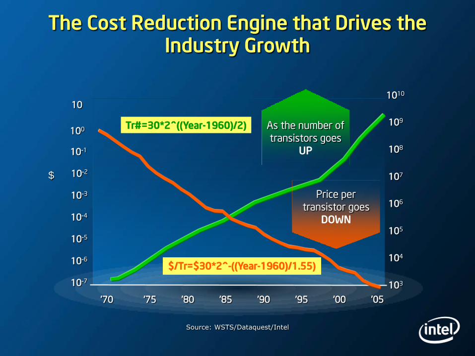
Source: WSTS/Dataquest/Intel
103
104
105
106
107
108
109
1010
’70 ’75 ’80 ’85 ’90 ’95 ’00 ’05
As the number of
transistors goes
UP
Price per
transistor goes
DOWN
10
10-6
10-5
10-4
10-3
10-2
10-1
100
10-7
$
The Cost Reduction Engine that Drives the Industry Growth
$/Tr=$30*2^-((Year-1960)/1.55)
Tr#=30*2^((Year-1960)/2)
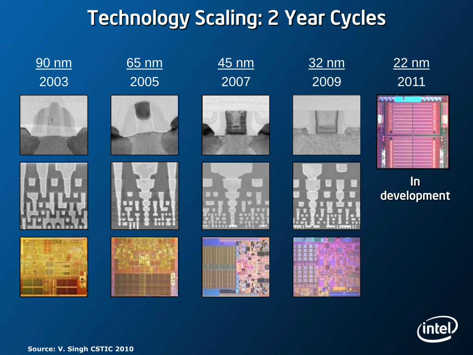
Technology Scaling: 2 Year Cycles
32 nm
2009
90 nm
2003
45 nm
2007
65 nm
2005
22 nm
2011
Indevelopment
Source: V. Singh CSTIC 2010
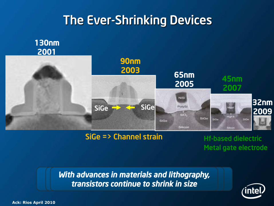
Strained silicon provided increased drive currents, making up for lack of gate oxide scaling
90nm2003
SiGe => Channel strain
SiGe SiGe
45nm2007
Hf-based dielectric
Metal gate electrode
High-k + metal gate transistors broke through the gate oxide scaling barrier
The Ever-Shrinking Devices
130nm2001
32nm2009
With advances in materials and lithography, transistors continue to shrink in size
65nm2005
Ack: Rios April 2010
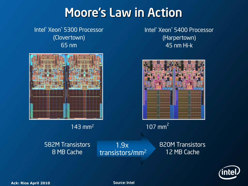
820M Transistors
12 MB Cache
107 mm2
143 mm2
582M Transistors
8 MB Cache
Intel® Xeon® 5300 Processor
(Clovertown)
65 nm
Intel® Xeon® 5400 Processor
(Harpertown)
45 nm Hi-k
1.9x transistors/mm2
Source: Intel
Moore‟s Law in Action
Ack: Rios April 2010
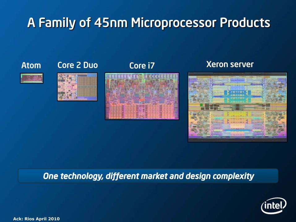
A Family of 45nm Microprocessor Products
Atom Core 2 Duo Xeron serverCore i7
One technology, different market and design complexity
Ack: Rios April 2010
Microprocessor Development
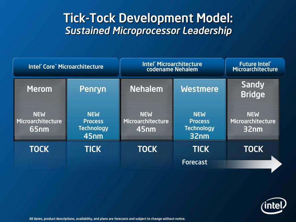
Tick-Tock Development Model:Sustained Microprocessor Leadership
All dates, product descriptions, availability, and plans are forecasts and subject to change without notice.
Forecast
Penryn NehalemSandyBridge
Westmere
NEWMicroarchitecture
45nm
NEWMicroarchitecture
32nm
NEWProcess
Technology
45nm
NEW Process
Technology
32nm
Merom
NEWMicroarchitecture
65nm
TOCK TICK TOCK TICK TOCK
Intel® Core™ Microarchitecture Intel® Microarchitecturecodename Nehalem
Future Intel®Microarchitecture
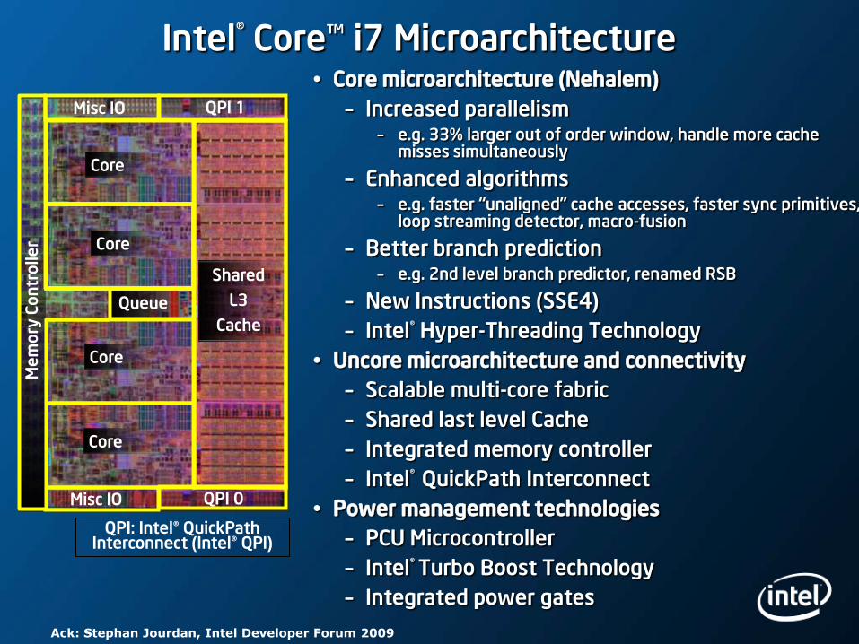
Intel® Core™ i7 Microarchitecture Core microarchitecture (Nehalem)
– Increased parallelism– e.g. 33% larger out of order window, handle more cache
misses simultaneously
– Enhanced algorithms– e.g. faster “unaligned” cache accesses, faster sync primitives,
loop streaming detector, macro-fusion
– Better branch prediction– e.g. 2nd level branch predictor, renamed RSB
– New Instructions (SSE4)
– Intel® Hyper-Threading Technology
Uncore microarchitecture and connectivity
– Scalable multi-core fabric
– Shared last level Cache
– Integrated memory controller
– Intel® QuickPath Interconnect
Power management technologies
– PCU Microcontroller
– Intel® Turbo Boost Technology
– Integrated power gates
QPI: Intel® QuickPath Interconnect (Intel® QPI)
Core
Shared
L3
Cache
Core
Core
Core
Queue
Misc IO QPI 0
Misc IO QPI 1
Me
mo
ry C
on
tro
lle
r
Ack: Stephan Jourdan, Intel Developer Forum 2009
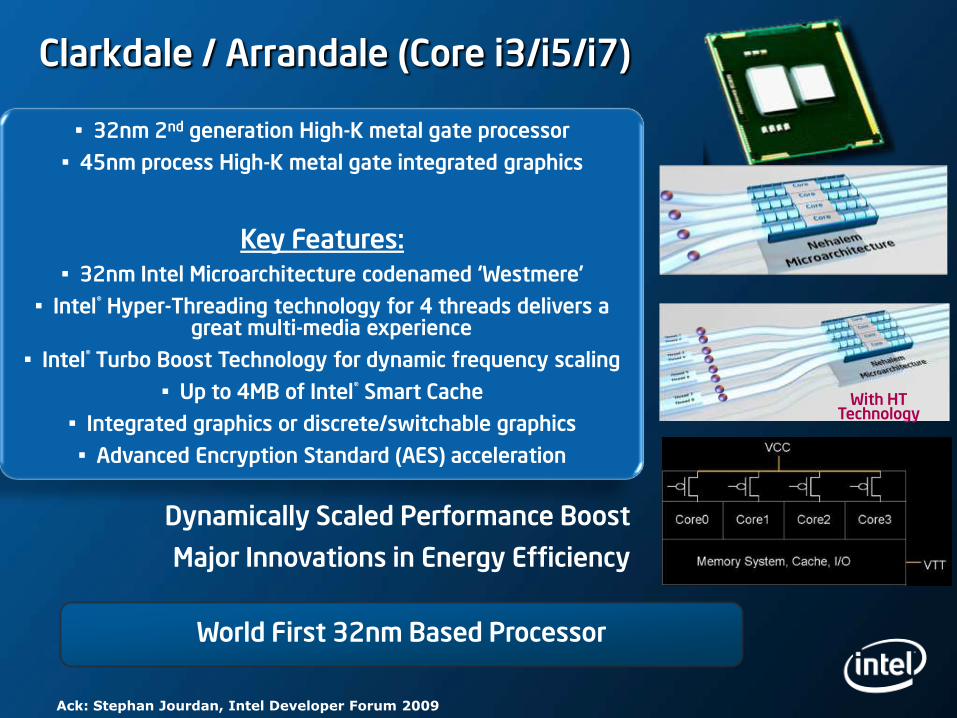
Clarkdale / Arrandale (Core i3/i5/i7)
World First 32nm Based Processor
• 32nm 2nd generation High-K metal gate processor
• 45nm process High-K metal gate integrated graphics
Key Features:
• 32nm Intel Microarchitecture codenamed „Westmere‟
• Intel® Hyper-Threading technology for 4 threads delivers a great multi-media experience
• Intel® Turbo Boost Technology for dynamic frequency scaling
• Up to 4MB of Intel® Smart Cache
• Integrated graphics or discrete/switchable graphics
• Advanced Encryption Standard (AES) acceleration
Ack: Stephan Jourdan, Intel Developer Forum 2009
With HT Technology
Dynamically Scaled Performance Boost
Major Innovations in Energy Efficiency
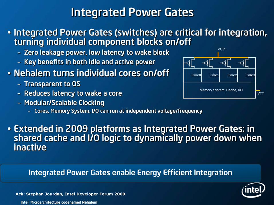
Integrated Power Gates
Integrated Power Gates (switches) are critical for integration, turning individual component blocks on/off
– Zero leakage power, low latency to wake block
– Key benefits in both idle and active power
Nehalem turns individual cores on/off– Transparent to OS
– Reduces latency to wake a core
– Modular/Scalable Clocking– Cores, Memory System, I/O can run at independent voltage/frequency
Extended in 2009 platforms as Integrated Power Gates: in shared cache and I/O logic to dynamically power down when inactive
Core0 Core1 Core2 Core3
Memory System, Cache, I/OVTT
VCC
Integrated Power Gates enable Energy Efficient Integration
Intel® Microarchitecture codenamed Nehalem
Ack: Stephan Jourdan, Intel Developer Forum 2009
Lithography: Driver to Enable Scaling
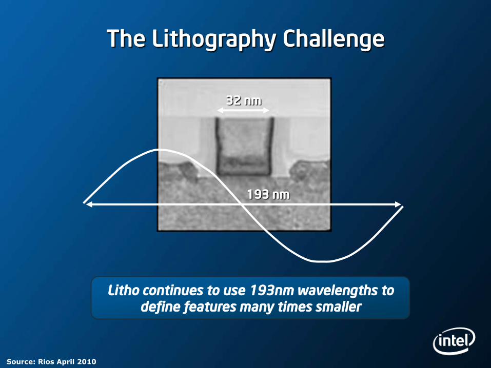
The Lithography Challenge
32 nm
Litho continues to use 193nm wavelengths to define features many times smaller
193 nm
Source: Rios April 2010
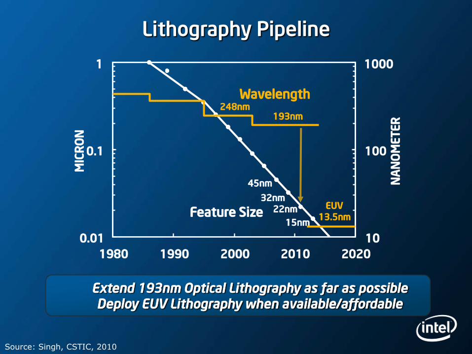
Lithography Pipeline
Source: Singh, CSTIC, 2010
Extend 193nm Optical Lithography as far as possibleDeploy EUV Lithography when available/affordable
0.01
0.1
1
1980 1990 2000 2010 2020
MIC
RO
N
10
100
1000
32nm
22nm
15nmFeature Size
Wavelength248nm
193nm
EUV
13.5nm
NA
NO
ME
TE
R
45nm
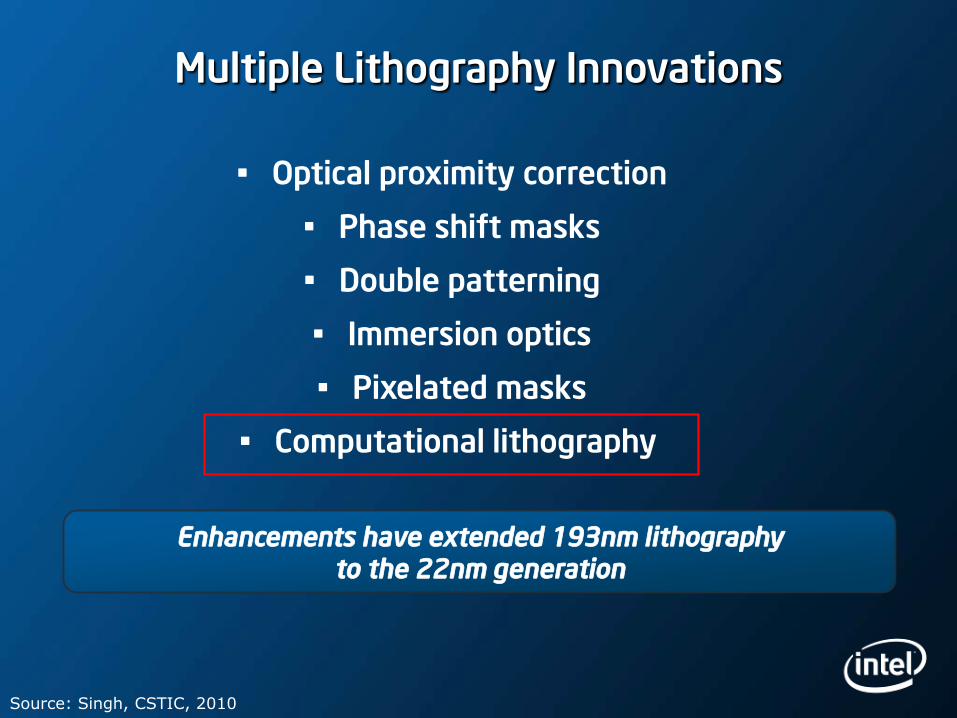
Multiple Lithography Innovations
Enhancements have extended 193nm lithography to the 22nm generation
• Optical proximity correction
• Phase shift masks
• Double patterning
• Immersion optics
• Pixelated masks
• Computational lithography
Source: Singh, CSTIC, 2010
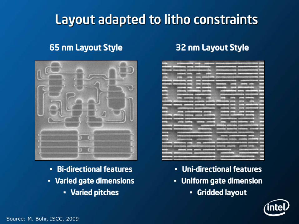
Layout adapted to litho constraints
65 nm Layout Style 32 nm Layout Style
• Bi-directional features
• Varied gate dimensions
• Varied pitches
• Uni-directional features
• Uniform gate dimension
• Gridded layout
Source: M. Bohr, ISCC, 2009
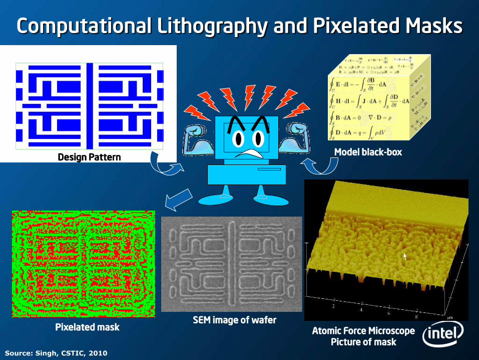
Computational Lithography and Pixelated Masks
Design Pattern
Pixelated maskSEM image of wafer
Atomic Force Microscope Picture of mask
Model black-box
Source: Singh, CSTIC, 2010
Process Modeling: Integrating material science, chemistry, mechanics …
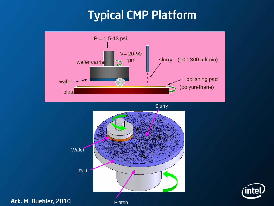
platen
slurry
wafer polishing pad
wafer carrier
P = 1.5-13 psi
(100-300 ml/min)V= 20-90
rpm
(polyurethane)
Typical CMP Platform
Platen
Pad
Wafer
Slurry
Ack. M. Buehler, 2010
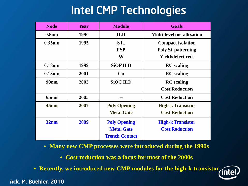
Intel CMP Technologies
Node Year Module Goals
0.8um 1990 ILD Multi-level metallization
0.35um 1995 STI
PSP
W
Compact isolation
Poly Si patterning
Yield/defect red.
0.18um 1999 SiOF ILD RC scaling
0.13um 2001 Cu RC scaling
90nm 2003 SiOC ILD RC scaling
Cost Reduction
65nm 2005 -- Cost Reduction
45nm 2007 Poly Opening
Metal Gate
High-k Transistor
Cost Reduction
32nm 2009 Poly Opening
Metal Gate
Trench Contact
High-k Transistor
Cost Reduction
• Many new CMP processes were introduced during the 1990s
• Cost reduction was a focus for most of the 2000s
• Recently, we introduced new CMP modules for the high-k transistor
Ack. M. Buehler, 2010
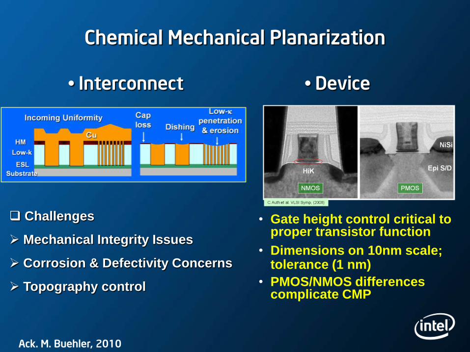
Chemical Mechanical Planarization
Interconnect Device
Challenges
Mechanical Integrity Issues
Corrosion & Defectivity Concerns
Topography control
• Gate height control critical to proper transistor function
• Dimensions on 10nm scale; tolerance (1 nm)
• PMOS/NMOS differences complicate CMP
Ack. M. Buehler, 2010
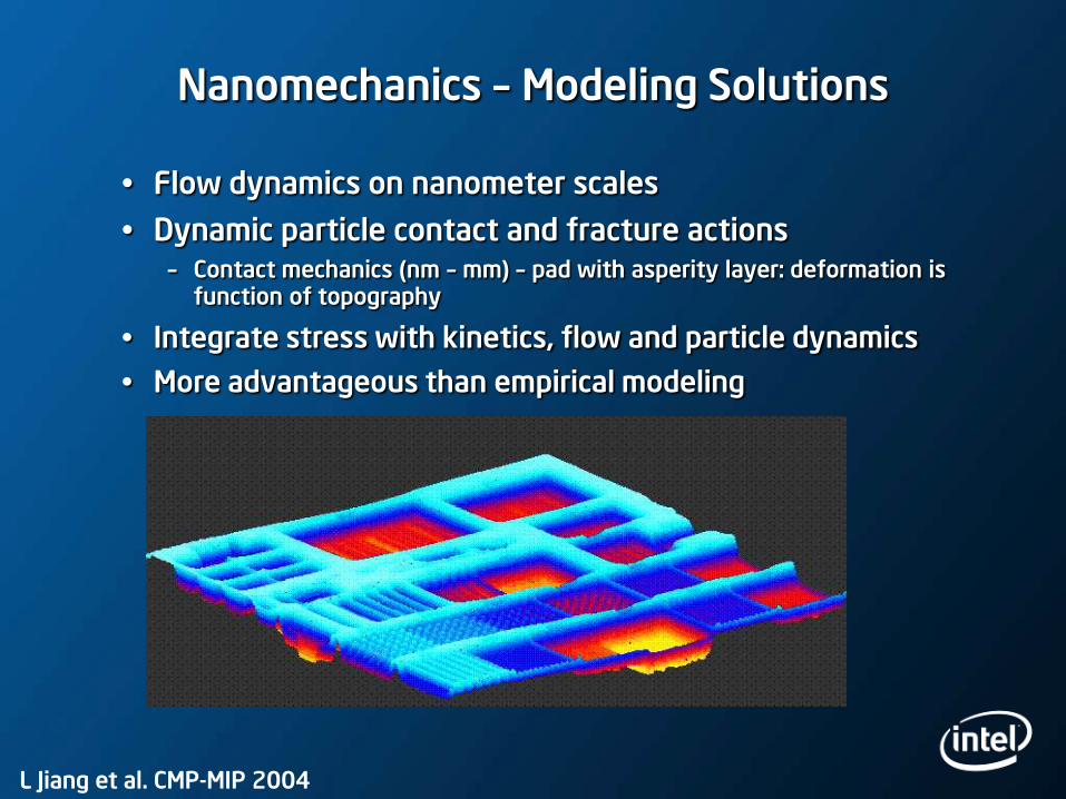
Nanomechanics – Modeling Solutions
Flow dynamics on nanometer scales
Dynamic particle contact and fracture actions– Contact mechanics (nm – mm) – pad with asperity layer: deformation is
function of topography
Integrate stress with kinetics, flow and particle dynamics
More advantageous than empirical modeling
L Jiang et al. CMP-MIP 2004

Reliability: Thermal Phenomena
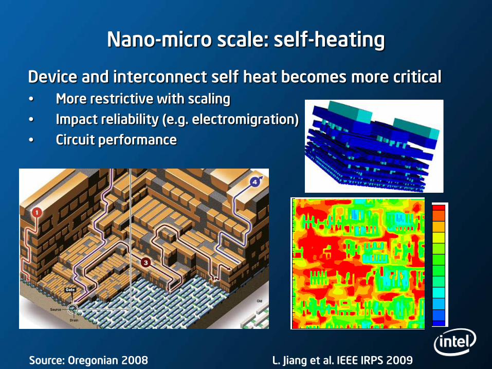
Nano-micro scale: self-heating
Device and interconnect self heat becomes more critical
More restrictive with scaling
Impact reliability (e.g. electromigration)
Circuit performance
L. Jiang et al. IEEE IRPS 2009Source: Oregonian 2008
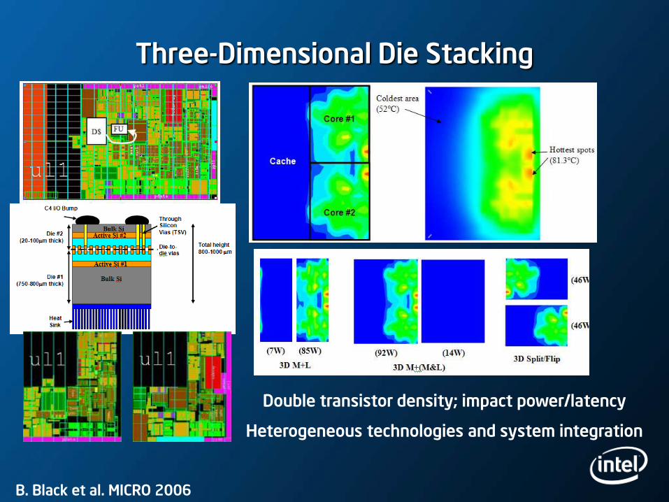
Three-Dimensional Die Stacking
Double transistor density; impact power/latency
Heterogeneous technologies and system integration
B. Black et al. MICRO 2006
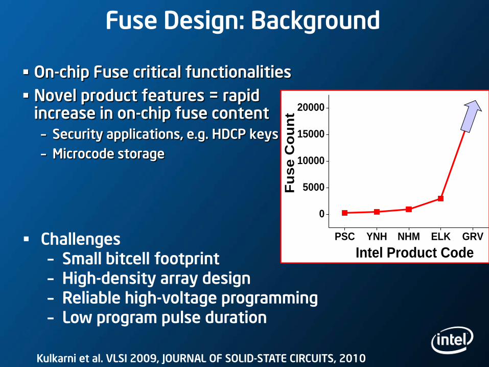
On-chip Fuse critical functionalities
Novel product features = rapid increase in on-chip fuse content
– Security applications, e.g. HDCP keys
– Microcode storage
Fuse Design: Background
Challenges – Small bitcell footprint– High-density array design– Reliable high-voltage programming– Low program pulse duration
PSC YNH NHM ELK GRV
0
5000
10000
15000
20000
Fu
se C
ou
nt
Intel Product Code
100+Kbit
Kulkarni et al. VLSI 2009, JOURNAL OF SOLID-STATE CIRCUITS, 2010
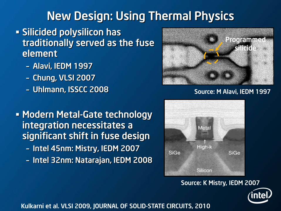
New Design: Using Thermal Physics
Silicided polysilicon has traditionally served as the fuse element
– Alavi, IEDM 1997
– Chung, VLSI 2007
– Uhlmann, ISSCC 2008
Modern Metal-Gate technology integration necessitates a significant shift in fuse design
– Intel 45nm: Mistry, IEDM 2007
– Intel 32nm: Natarajan, IEDM 2008
Programmedsilicide
Source: M Alavi, IEDM 1997
Source: K Mistry, IEDM 2007
Kulkarni et al. VLSI 2009, JOURNAL OF SOLID-STATE CIRCUITS, 2010
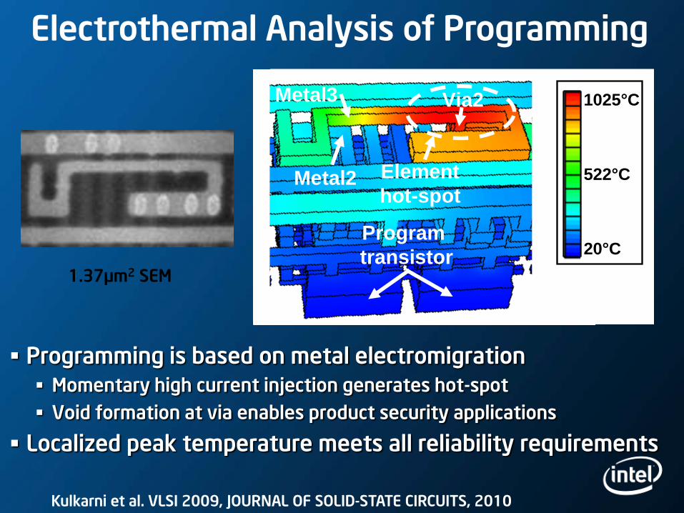
Programming is based on metal electromigration
Momentary high current injection generates hot-spot
Void formation at via enables product security applications
Localized peak temperature meets all reliability requirements
LT
D A
dv
an
ced
De
sig
nL
TD
Ad
van
ced
De
sig
nL
TD
Ad
van
ced
De
sig
nMetal Fuse Element Design
1025°C
522°C
20°C
Element
hot-spot
Via2
Program
transistor
Metal2
Metal3
1.37µm2 Metal-Fuse Bit Cell featuring a
3-D 1-Transistor 1-Resistor (1T1R) Topology
Electrothermal Analysis of Programming
1.37µm2 SEM
Kulkarni et al. VLSI 2009, JOURNAL OF SOLID-STATE CIRCUITS, 2010
Interconnect Reliability: Drivers for Thermo-Mechanical failures
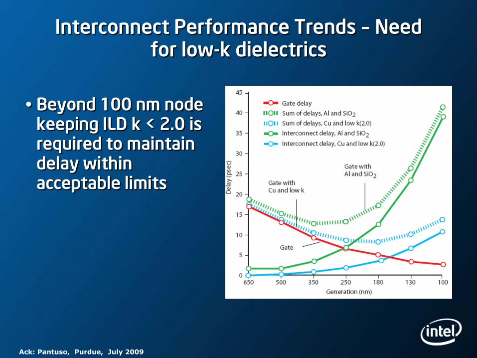
Interconnect Performance Trends – Need for low-k dielectrics
Beyond 100 nm node keeping ILD k < 2.0 is required to maintain delay within acceptable limits
Ack: Pantuso, Purdue, July 2009
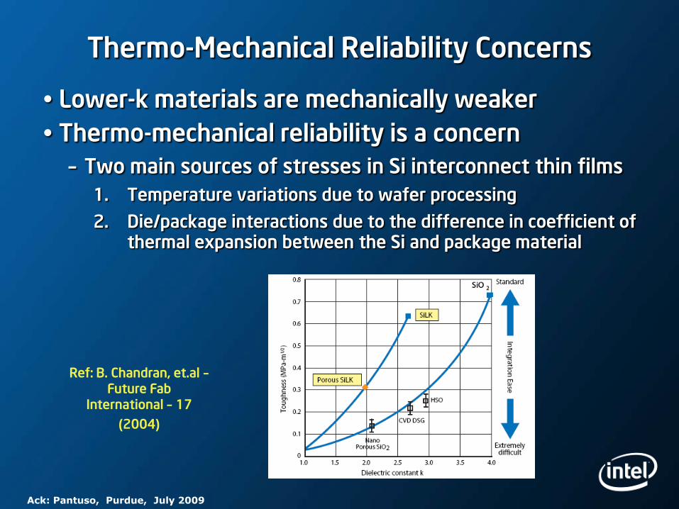
Thermo-Mechanical Reliability Concerns
Lower-k materials are mechanically weaker
Thermo-mechanical reliability is a concern
– Two main sources of stresses in Si interconnect thin films
1. Temperature variations due to wafer processing
2. Die/package interactions due to the difference in coefficient of thermal expansion between the Si and package material
Ref: B. Chandran, et.al –Future Fab
International – 17
(2004)
Ack: Pantuso, Purdue, July 2009
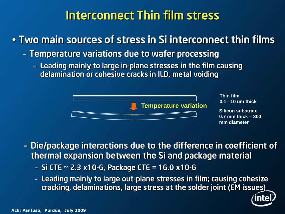
Interconnect Thin film stress
Two main sources of stress in Si interconnect thin films
– Temperature variations due to wafer processing
– Leading mainly to large in-plane stresses in the film causing delamination or cohesive cracks in ILD, metal voiding
Silicon substrate
0.7 mm thick – 300
mm diameter
Thin film
0.1 - 10 um thickTemperature variation
– Die/package interactions due to the difference in coefficient of thermal expansion between the Si and package material
– Si CTE ~ 2.3 x10⁻⁶, Package CTE = 16.0 x10⁻⁶
– Leading mainly to large out-plane stresses in film; causing cohesize cracking, delaminations, large stress at the solder joint (EM issues)
Ack: Pantuso, Purdue, July 2009
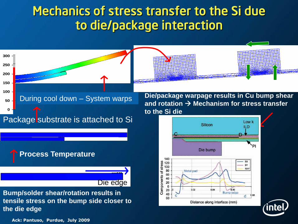
Mechanics of stress transfer to the Si due to die/package interaction
Package substrate is attached to Si
During cool down – System warps Die/package warpage results in Cu bump shear
and rotation Mechanism for stress transfer
to the Si die
Die edge
Bump/solder shear/rotation results in
tensile stress on the bump side closer to
the die edge
Ack: Pantuso, Purdue, July 2009
0
50
100
150
200
250
300
1 2 3 4 5 6 7 8 9 10
Series1
0
50
100
150
200
250
300
1 2 3 4 5 6 7 8 9 10
Series1
Process Temperature
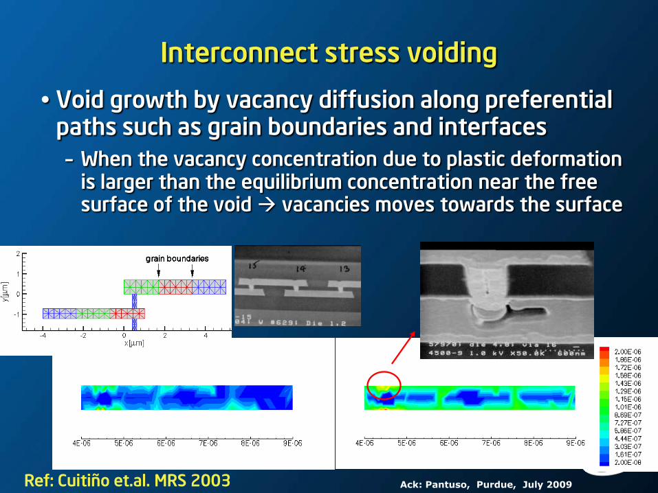
Interconnect stress voiding
Void growth by vacancy diffusion along preferential paths such as grain boundaries and interfaces
– When the vacancy concentration due to plastic deformation is larger than the equilibrium concentration near the free surface of the void vacancies moves towards the surface
Ref: Cuitiño et.al. MRS 2003 Ack: Pantuso, Purdue, July 2009
Summary
Source: Garcia July 2010
Intel continues relentless pursuit of scaling
CAD continutes to be play key role to lithography, device, and process integration
Reliability and variation simply become more challenging at leading edge technology
Modeling helps set direction for disruptive technology and design of new circuit
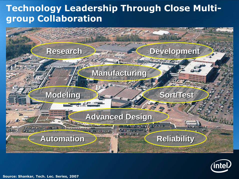
Research Development
Manufacturing
Sort/Test
Automation Reliability
Modeling
Advanced Design
Technology Leadership Through Close Multi-group Collaboration
Source: Shankar, Tech. Lec. Series, 2007
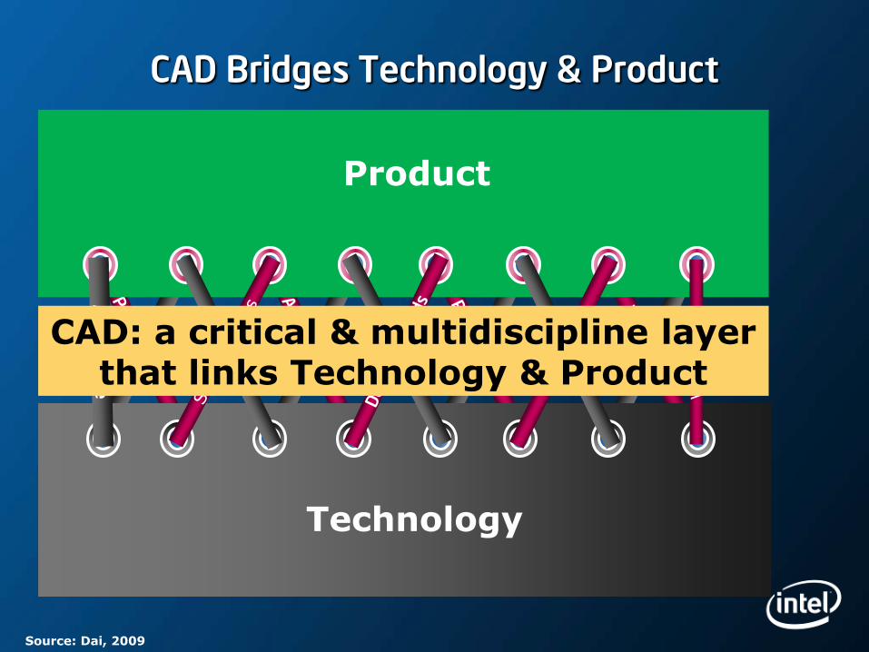
CAD Bridges Technology & Product
Veri
fication
Product
Technology
CAD: a critical & multidiscipline layer that links Technology & Product
Source: Dai, 2009
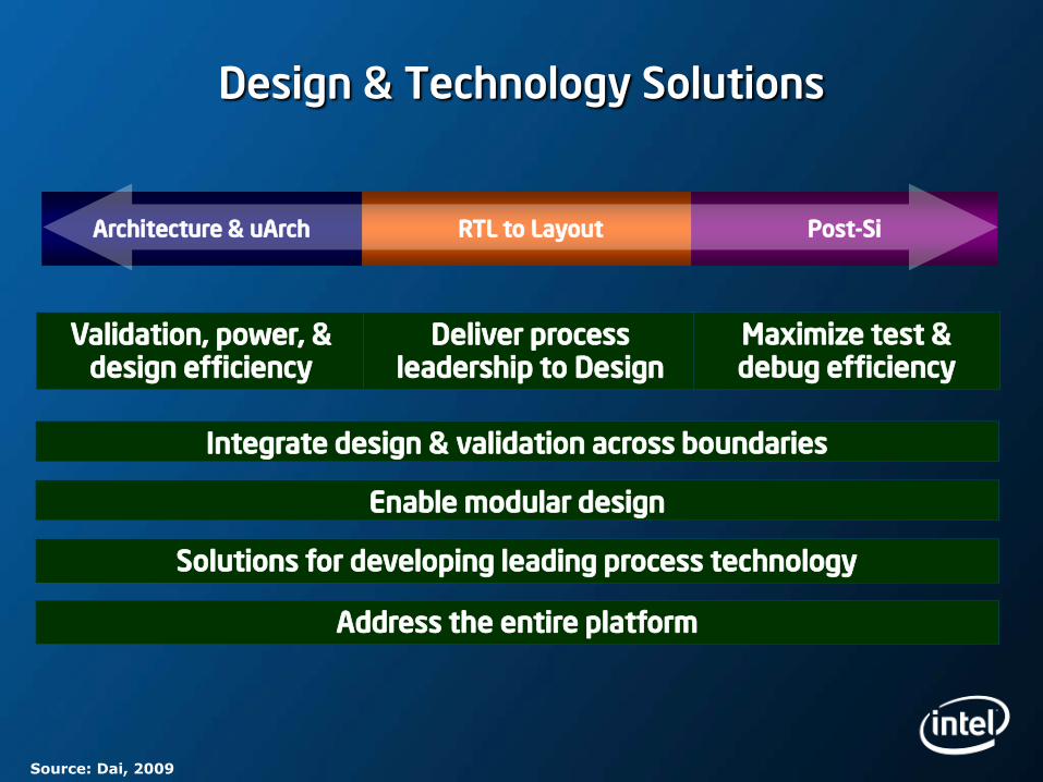
Design & Technology Solutions
Architecture & uArch RTL to Layout Post-Si
Validation, power, & design efficiency
Deliver process leadership to Design
Maximize test & debug efficiency
Integrate design & validation across boundaries
Enable modular design
Solutions for developing leading process technology
Address the entire platform
Source: Dai, 2009
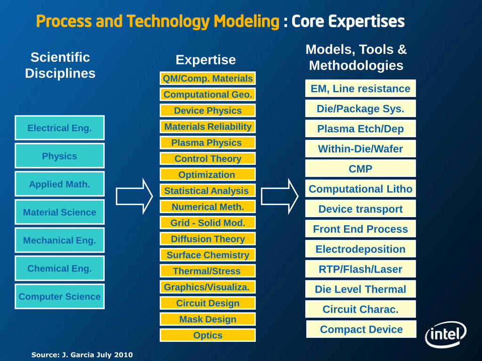
Electrical Eng.
Physics
Chemical Eng.
Mechanical Eng.
Computer Science
Applied Math.
Material Science
Scientific
DisciplinesExpertise
Models, Tools &
Methodologies
Process and Technology Modeling : Core Expertises
RTP/Flash/Laser
Die Level Thermal
Die/Package Sys.
EM, Line resistance
Within-Die/Wafer
Front End Process
CMP
Computational Litho
Plasma Etch/Dep
Device transport
Electrodeposition
Control Theory
QM/Comp. Materials
Device Physics
Computational Geo.
Materials Reliability
Grid - Solid Mod.
Diffusion Theory
Numerical Meth.
Surface Chemistry
Thermal/Stress
Graphics/Visualiza.
Optimization
Plasma Physics
Statistical Analysis
Circuit Design
Mask Design
Optics
Circuit Charac.
Compact Device
Source: J. Garcia July 2010
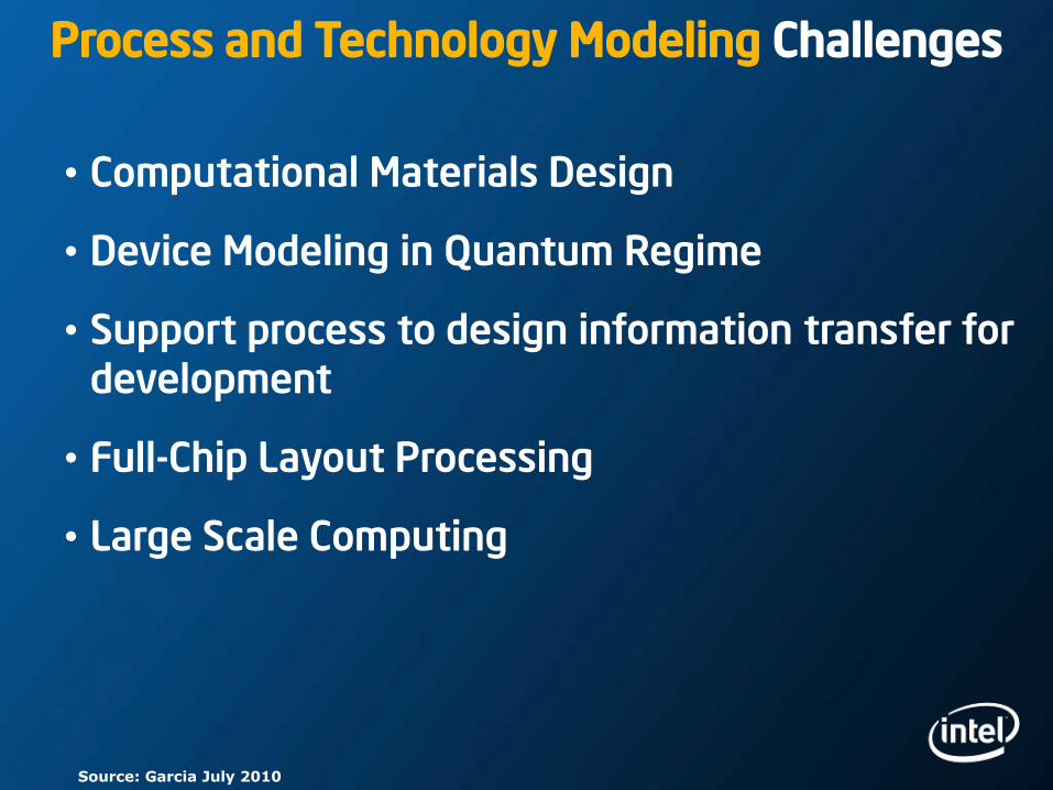
Process and Technology Modeling Challenges
• Computational Materials Design
• Device Modeling in Quantum Regime
• Support process to design information transfer for development
• Full-Chip Layout Processing
• Large Scale Computing
Source: Garcia July 2010
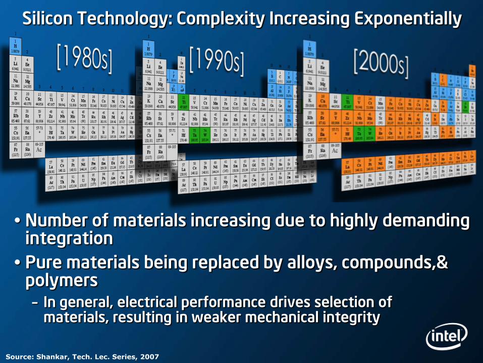
Silicon Technology: Complexity Increasing Exponentially
Number of materials increasing due to highly demanding integration
Pure materials being replaced by alloys, compounds,& polymers– In general, electrical performance drives selection of
materials, resulting in weaker mechanical integrity
Source: Shankar, Tech. Lec. Series, 2007
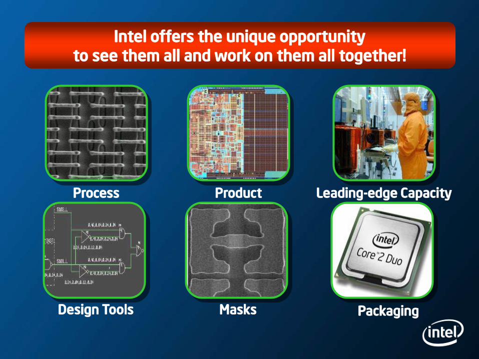
Leading-edge Capacity
Packaging
Process Product
Design Tools Masks
Intel offers the unique opportunity to see them all and work on them all together!

Words of Wisdom to Follow
“No exponential is
forever … but we can
delay „forever‟.”
Gordon Moore
ISSCC
2003