Embed Size (px)
Citation preview

ENGN3227: Analogue Electronics, By Group TA2
ENGN3227: Analogue Electronics Project
Voltage to frequency converter
By Group TA2:
Bathiya Senanayake. ID: u3957406 Rabie Soukieh, ID: u4113369 Samuel Gilligan, ID: u4111478
Lecturer: Dr Salman Durrani
1

ENGN3227: Analogue Electronics, By Group TA2
Table of Contents Table of Contents ................................................................................................................................................... 2 1 Abstract .......................................................................................................................................................... 3 2 Introduction .................................................................................................................................................... 4 3 Theory/Design ................................................................................................................................................ 4
3.1 Design ................................................................................................................................................... 4 3.1.1 Keypad interface circuit.................................................................................................................... 5 3.1.2 Digital to Analog Conversion ........................................................................................................... 5 3.1.3 AD650 .............................................................................................................................................. 7 3.1.4 Frequency dividers and multiplexers.............................................................................................. 10 3.1.5 Output level control ........................................................................................................................ 10
4 Implementation............................................................................................................................................. 10 5 Results .......................................................................................................................................................... 12 6 Conclusion.................................................................................................................................................... 14 7 Appendix A: Labelled photographs of assembled breadboard and PCB circuit .......................................... 15 8 Appendix B: Pspice Implementation............................................................................................................ 22
8.1 AD650................................................................................................................................................. 22 8.2 Keypad ................................................................................................................................................ 23
8.2.1 Keypad Simulation ......................................................................................................................... 28
2

ENGN3227: Analogue Electronics, By Group TA2
1 Abstract Today’s integrated circuit industry provides a wide array of devices which allow the conversion of a quantity from one domain to another. Conversion between voltage and frequency is a common requirement in areas such as in the remote sensing of a quantity (temperature, pressure, and level), digital voltmeters and most radio frequency (RF) applications. Devices which can perform this task are known as voltage to frequency converters, and are often referred to as voltage controlled oscillators (VCO). The AD650 IC is an example of a VCO implemented as an integrated chip package, providing highly linear voltage to frequency conversion over a large range. A keypad/rotary switch input and three LED displays were used in conjunction with the AD650 to provide a user interface. The bread boarding phase revealed certain areas for improvement. Pspice simulations of the circuit allowed a conformation of the original and revised designs. The practical output of the AD650, after testing the PCBs was found to be less than 500 kHz. Factors which are likely to have caused this shift in performance are a 400 kHz noise component on the AD650 input, and that the AD650 became non-linear for frequencies above 500 kHz. This was not the intended operating range of the AD650, as it should have been able to output frequencies up to 1 MHz. The drop in the operating range suggests a problem with the PCB implementation and that not all factors were considered when designing the PCBs. Such factors include RF design methodology. In spite of this drawback, the final implementation operates up to the mentioned range, and can still be used as a voltage to frequency converter.
3
ENGN3227: Analogue Electronics, By Group TA2
2 Introduction
3 Theory/Design
An important attribute of any engineer is that they are independent in gathering information and applying their knowledge in an engineering design. This involves communicating effectively with others in a team to accomplish a common goal. The analogue electronics project requires these attributes and acquaints students with the modern applications and implementation of analogue electronics. The project requires the use of ADC/DAC, op-amps or 555 timers and challenges students to produce a design at minimal cost. A common interest amongst team members was the voltage controlled oscillator (VCO) which allows voltage to frequency conversion, or frequency to voltage conversion. It can also be configured as a DAC or an ADC, and can be used as a frequency modulator. It was decided that the VCO should be implemented as a voltage to frequency converter. As an addition to the VCO, the design was revised several times to include extra features such as a display unit and an input interface. The purpose of these additions is to create an interactive environment so that it is easier to use the VCO, understand the conversion process, and to make the project more challenging and interesting. As a result of these extra features, the circuitry for the design had to be separated into several modules. The first and perhaps most challenging part of the circuit was the input interface. The first interface developed included a keypad, a keypad polling circuit (including a 555 timer), range selector, enter detector, and decimal point and number of digits display settings. The keys entered from the keypad needed to be converted to BCD logic to be used by the shift registers and adders. In order to do this a keypad to BCD decoder was designed. The circuitry necessary to perform these operations mainly required the use of digital electronics. Due to the complexity of implementing and testing the keypad circuitry and the limited time available, another input interface was developed and implemented. This was to replace the keypad if it were not completed on time. A total of three rotary switches were included to allow the input voltage to be set. A further discussion and comparison between the two input designs is given later in the report. The input to the VCO requires an analog voltage. To ensure that the correct analog signal is set, DACs are used to convert from a digital to analog current. Op-amps are used to convert from this current to voltage, and several other op-amps perform scaling before this voltage is sent to the input of the VCO. The AD650 VCO was chosen as the voltage to frequency converter. The range of frequencies that the AD650 can output depends on how it is calibrated. The output frequency of the AD650 relates to the input current, a one shot capacitor, and an integrating capacitor which all determine the period of the output signal. The theory required to set these values is available in the course text book (Floyd, Buchla, “Fundamentals of analog circuits”, pp 743-746) To select between the Hz and kHz frequency ranges, three decade counters were used as frequency dividers at the output of the AD650, to provide a divide by 1000. A multiplexer was used to enable either the divide by 1000 for the Hz range or output directly from the AD650 for the kHz range.
3.1 Design The voltage to frequency converter was designed in a modular fashion. As such the designs of each module were designed separately. The keypad circuit is the interface to the V/F converter, allows a user to specify a three digit frequency either in Hz or KHz range. The keypad digit presses was stored in three shift registers,
4
ENGN3227: Analogue Electronics, By Group TA2
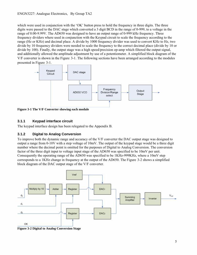
which were used in conjunction with the ‘OK’ button press to hold the frequency in three digits. The three digits were passed to the DAC stage which converted a 3 digit BCD in the range of 0-999, to a voltage in the range of 0.00-9.99V. The AD650 was designed to have an output range of 0-999 kHz frequency. Three frequency dividers where used in conjunction with the Keypad circuit to scale the frequency according to the range (Hz or KHz) and decimal place. A divide by 1000 frequency divider was used to convert KHz to Hz, two divide by 10 frequency dividers were needed to scale the frequency to the correct decimal place (divide by 10 or divide by 100). Finally, the output stage was a high speed/precision op-amp which filtered the output signal, and additionally allowed the amplitude adjustment by use of a potentiometer. A simplified block diagram of the V/F converter is shown in the Figure 3-1. The following sections have been arranged according to the modules presented in Figure 3-1.
Figure 3-1 The V/F Converter showing each module
3.1.1 Keypad interface circuit The keypad interface design has been relegated to the Appendix B.
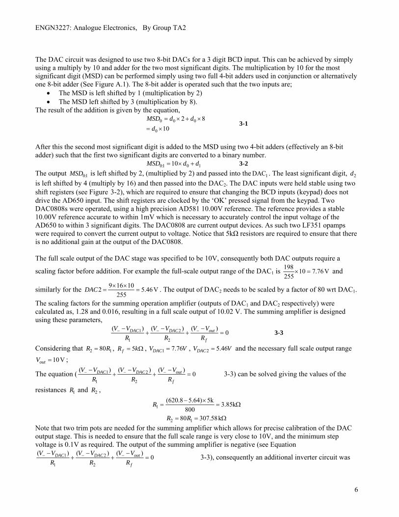
3.1.2 Digital to Analog Conversion To improve both the dynamic range and accuracy of the V/F converter the DAC output stage was designed to output a range from 0-10V with a step voltage of 10mV. The output of the keypad stage would be a three digit number where the decimal point is omitted for the purposes of Digital to Analog Conversion. The conversion factor of the three digit input to voltage input stage of the AD650 was specified to be 10mV per unit. Consequently the operating range of the AD650 was specified to be 1KHz-999KHz, where a 10mV step corresponds to a 1KHz change in frequency at the output of the AD650. The Figure 3-2 shows a simplified block diagram of the DAC output stage of the V/F converter.
Figure 3-2 Digital to Analog Conversion Stage
5
ENGN3227: Analogue Electronics, By Group TA2
The DAC circuit was designed to use two 8-bit DACs for a 3 digit BCD input. This can be achieved by simply using a multiply by 10 and adder for the two most significant digits. The multiplication by 10 for the most significant digit (MSD) can be performed simply using two full 4-bit adders used in conjunction or alternatively one 8-bit adder (See Figure A.1). The 8-bit adder is operated such that the two inputs are;
• The MSD is left shifted by 1 (multiplication by 2) • The MSD left shifted by 3 (multiplication by 8).
The result of the addition is given by the equation, 0 0 0
0
2 810
MSD d dd
= × + ×
= × 3-1
After this the second most significant digit is added to the MSD using two 4-bit adders (effectively an 8-bit adder) such that the first two significant digits are converted to a binary number.
0:1 0 110MSD d d= × + 3-2 The output 0:1MSD is left shifted by 2, (multiplied by 2) and passed into the . The least significant digit, is left shifted by 4 (multiply by 16) and then passed into the DAC
1DAC 2d
2. The DAC inputs were held stable using two shift registers (see Figure 3-2), which are required to ensure that changing the BCD inputs (keypad) does not drive the AD650 input. The shift registers are clocked by the ‘OK’ pressed signal from the keypad. Two DAC0808s were operated, using a high precision AD581 10.00V reference. The reference provides a stable 10.00V reference accurate to within 1mV which is necessary to accurately control the input voltage of the AD650 to within 3 significant digits. The DAC0808 are current output devices. As such two LF351 opamps were required to convert the current output to voltage. Notice that 5kΩ resistors are required to ensure that there is no additional gain at the output of the DAC0808. The full scale output of the DAC stage was specified to be 10V, consequently both DAC outputs require a
scaling factor before addition. For example the full-scale output range of the DAC1 is 198 10 7.76V255
× = and
similarly for the 9 16 102255
DAC × ×= = 5.46V . The output of DAC2 needs to be scaled by a factor of 80 wrt DAC1.
The scaling factors for the summing operation amplifier (outputs of DAC1 and DAC2 respectively) were calculated as, 1.28 and 0.016, resulting in a full scale output of 10.02 V. The summing amplifier is designed using these parameters,
1 2
1 2
( ) ( ) ( )0DAC DAC out
f
V V V V V VR R R
− − −− − −+ + = 3-3
Considering that , , 2 180R R= 5fR k= Ω 1 7.76DACV V= , 2 5.46DACV V= and the necessary full scale output range ; 10VoutV =
The equation ( 1 2
1 2
( ) ( ) ( )0DAC DAC out
f
V V V V V VR R R
− − −− − −+ + = 3-3) can be solved giving the values of the
resistances and , 1R 2R
1(620.8 5.64) 5k 3.85k
800R − ×
= = Ω
2 180 307.58kR R= = Ω Note that two trim pots are needed for the summing amplifier which allows for precise calibration of the DAC output stage. This is needed to ensure that the full scale range is very close to 10V, and the minimum step voltage is 0.1V as required. The output of the summing amplifier is negative (see Equation
1 2
1 2
( ) ( ) ( )0DAC DAC out
f
V V V V V VR R R
− − −− − −+ + = 3-3), consequently an additional inverter circuit was
6
ENGN3227: Analogue Electronics, By Group TA2
needed to simply invert the output. The inverting circuit is simply an inverting amplifier, where the gain is given by,
fout in
i
RV V
R= − 3-4
Obviously the resistance ratio for the inverting amplifier, 1f
i
RR
= . An additional design improvement would be
to simply alter the inverting amplifier to be a active low pass filter by adding a capacitance across fR . This would reduce any noise at the input to the AD650, considering that the input to the AD650 is very low frequency and can be considered to be approximately DC (refer to implementation).
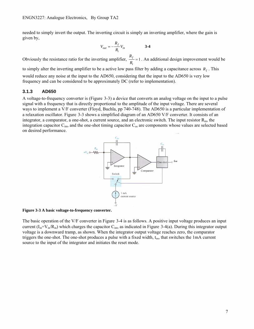
3.1.3 AD650 A voltage-to-frequency converter is (Figure 3-3) a device that converts an analog voltage on the input to a pulse signal with a frequency that is directly proportional to the amplitude of the input voltage. There are several ways to implement a V/F converter (Floyd, Buchla, pp 740-748). The AD650 is a particular implementation of a relaxation oscillator. Figure 3-3 shows a simplified diagram of an AD650 V/F converter. It consists of an integrator, a comparator, a one-shot, a current source, and an electronic switch. The input resistor Rin, the integration capacitor Cint, and the one-shot timing capacitor Cos are components whose values are selected based on desired performance.
Figure 3-3 A basic voltage-to-frequency converter. The basic operation of the V/F converter in Figure 3-4 is as follows. A positive input voltage produces an input current (Iin=Vin/Rin) which charges the capacitor Cint, as indicated in Figure 3-4(a). During this integrator output voltage is a downward tramp, as shown. When the integrator output voltage reaches zero, the comparator triggers the one-shot. The one-shot produces a pulse with a fixed width, tos, that switches the 1mA current source to the input of the integrator and initiates the reset mode.
7

ENGN3227: Analogue Electronics, By Group TA2
Figure 3-4 (Floyd, Buchla, pp 740-748) During the reset mode, current through the capacitor is in the opposite direction from the integrate mode, as indicated in Figure 3-4(b). This produces an upward ramp on the integrator output as indicated. After the one-shot times out, the current source is switched back to the integrator output, initializing another integrate mode and the cycle repeats. If the input voltage is held constant, the output waveform of the integrator is as shown in Figure 3-5, where the amplitude and the integrate time remain constant. The final output of the V/F converter is taken off the one-shot, as indicated in Figure 3-5. As long as the input voltage is constant, the output pulse stream has a constant frequency. An increase in the input voltage, , causes the input current, , to increase. In the basic relationship , the term is the slope of the capacitor voltage. If the current increases, also increases since C is constant. As applied to the V/F converter, this means that if the input current ( ) increases, then the slope of the integrator output during the integrate mode will also increase and reduce the period of the final output voltage. Also, during the reset mode, the opposite current through the capacitor, 1mA-
, is smaller, thus decreasing the slope of the upward ramp and reducing the amplitude of the integrator output voltage.
inV inI( / )C CI V t= C /CV t /CV t
inI
inI
Figure 3-5 (Floyd, Buchla, pp 740-748)
8

ENGN3227: Analogue Electronics, By Group TA2
The AD650 is an example of a V/F converter very similar to the basic device that was just discussed. The main differences in the AD650 are the output transistor and the comparator threshold voltage of -0.6 V instead of ground. The values of the external components of the AD650 determine the operating characteristics of the device. The AD650 circuit was designed to operate from 1kHz-1Mhz. Knowing that the output voltage of the DAC stage is within the range of 0.1-10 V, means that the AD650 needs to be calibrated such that a 0.1V step at the input, results in a change in frequency of 1kHz at the output. The crucial characteristic about the AD650 is that it has a linear scale for voltage to frequency. The values of the external components determine the operating characteristics of the device. The pulse width of the one-shot output is set by the following formula:
3(6.8 10 / ) 3 10os ost C s F −= × + × 7 s 3-5 During the reset interval, the integrator output voltage increases by an amount expressed as,
in os
int
(1mA )V
I tC−
Δ = 3-6
The duration of the integrate interval when the integrator output is sloping downward is int
intin int int
int
(1mA )// /
1mA 1
os in
in
osin
t IVtI C I C
t tI
−Δ= =
⎛ ⎞= −⎜ ⎟⎝ ⎠
C
3-7
The period of a full cycle consists of the reset interval plus the integrate interval.
int1mA 1mA1os os os os
in inT t t t t t
I I⎛ ⎞ ⎛
= + = + − =⎜ ⎟ ⎜⎝ ⎠ ⎝
⎞⎟⎠
3-8
Therefore, the output frequency can be expressed as
( )1mAin
os
If
t= 3-9
The equation (( )1mA
in
os
If
t= 3-9) shows that the frequency is directly proportional to the input
current; and since , it is also directly proportional to the input voltage and inversely proportional to the input resistance. Knowing that the maximum frequency output is 1MHz, the duty cycle of the output at 1MHz was specified to be ~50% nominally. To maintain as close to 50% duty cycle at 1MHz, the closest possible value for was chosen, resulting in
/in in inI V R=
47pFosC = 0.62 μsost = . Consequently the duty cycle at 1 MHz is 62%. Now solving for the full scale input current to maintain 1Mhz output, (1mA) 0.62mAin osI f t= × = . Solving for the value of , inR
Ω / 10 / 0.62mA=16.13kin in inR V I V= =An additional trim pot was used in series with to allow for precise calibration inRThe Table 3-1 shows the final external components chosen for the AD650 circuit. Figure 3-6 shows the designed AD650 circuit with external components.
Component Value Rin 16.2 kΩ Cint 2.2 nF Cos 47 pF
Table 3-1
9

ENGN3227: Analogue Electronics, By Group TA2
Figure 3-6
3.1.4 Frequency dividers and multiplexers Frequency dividers were used to achieve the specified dynamic range 1.00Hz-999KHz. A divide by 1000 frequency divider was used to determine the range Hz/KHz. The decimal point decoder logic along with the two divide by 10 frequency dividers were used to convert the output of the AD650 to the correct range. The Figure A.1 of appendix A, shows the frequency dividers used in conjunction with a number of multiplexers.
3.1.5 Output level control The output of the frequency dividers was passed through a high-precision op-amp circuit which is shown in Figure A.1 of appendix A. The LM318 is a high-speed/precision op-amp needed to clean the pulse width output, and additionally a capacitor was connected in the feedback to provide filtering at >> 1 MHz. A 10kΩ potentiometer was used to allow the output amplitude to be decreased from 5V to 0V. Note also that the output of the op-amp is inverted.
4 Implementation The input interface consisted of several individual circuits to take the input from the keypad and process it for the rest of the circuit. Initially, the only parts of the keypad interface that were bread boarded were the keypad and the BCD to binary decoder. Several problems were encountered during this implementation and the design was revised accordingly. The output of the decoder was a 4 bit binary number. The decoded BCD has the corresponding value to the key pressed. At this stage, none of the other keypad circuits had been successfully implemented, mainly because of the time required to get the decoder to work.
As an alternative to the keypad interface, an input consisting of three BCD DIL rotary switches was developed. There was no available documentation for the rotary switches. As a precautionary measure, one of the switches was used as the test dummy. Before connecting the switch to any other components, it was tested by applying +5V, -5V and 0V inputs and observing the output. After several attempts, it was found that each switch has a grounded input and a four bit output. The digits 1-9 are output with floating values for the “low” bits and 0(ground) is “high”. These input digits are to be displayed on the LEDs, but the LEDs require positive logic. To solve this problem, all of the outputs for the three rotary switches were connected to inverters, whose outputs are active high.
10

ENGN3227: Analogue Electronics, By Group TA2
In the process of bread boarding the frequency dividers at the output of the AD650, some of the outputs were overloaded. Initially it seemed as though the outputs on two of the decade counters no longer functioned, though after waiting a week and then performing several tests with the oscilloscope, no damage could be found. This was presumably due to the effect of proprietary circuit protection inside the IC cutting the outputs due to current overload and then re-enabling them at a later time. The high precision, high speed op-amp at the output of the entire circuit was damaged by static. It was connected as an inverting op-amp with a low pass filer in the feedback network. The op-amp was found to be non-operational after it was first hooked up, indicating that it was already damaged, most likely by static. It was replaced and included in the PCB design. However, the new op-amp was overheated due to a mix up in the power rails on the PCB. As a result of this, it could not be included in the final implementation. A voltage reference is used to set the input to the DACs. The required reference for the DACs is 10V. To set this reference voltage, a potentiometer was connected to pin 1 of the voltage reference. This allowed the tuning of the voltage reference to a constant 10V. To provide a full scale output of 10V, the summing amplifier at the output of the DACs had to be calibrated. This was done by tuning the pots leading to the inverting input of the op-amp. Both 10kΩ and 500Ω variable resistors were used to set the full scale output to 10V. The current to voltage converters at the output of the DACs also had variable resistors in the feedback loop, to make the feedback resistance 5kΩ. These were omitted from the design, because this resistance is accounted for by the pots at the input of the summing amplifier, as discussed above. As discussed in the text book (Floyd, Buchla, pp 744), the frequency output of the AD650 is proportional to the input current. Therefore it is also proportional to the input resistance. To provide a fast method of testing the AD650, a potentiometer was connected to the input, rather than a single resistance. This allows the input current and voltage to the AD650 to be varied, and hence allows the frequency of the output to be controlled. To make sure that the AD650 was not outputting a frequency above 0Hz when an input of 0V was keyed in, another potentiometer was used at the offset inputs (pins 13 and 14) of the AD650. This was to allow adjustment of the offset, if there were any discrepancies in the output frequencies. It was also found that there was a 400KHZ 1Vpp noise waveform appearing on the op-amps located on the AD650 PCB. This noise was independent of the AD650 frequency, suggesting the oscillation was originating from some other source on the board. It was attempted to minimise this noise by implementing a low-pass active filter, however this did not reduce the signal by the theoretical amount. It was decided that the 400KHZ noise oscillation was the result of feedback amongst the many op-amps along with the lack of RF design in the PCBs. After the bread boarded implementation of the voltage to frequency converter was tested, confirmed (simulated) and completed, the next stage in the project was to transfer the design to a printed circuit board. The circuit was initially designed using Eagle software. This was convenient because Eagle has a PCB design tool. The only available Eagle software was trial ware. This meant that the PCB designs could not be bigger than about 10cm x 15cm. To transfer the voltage to frequency converter to a PCB implementation, it was split up into three PCB boards. The three schematics for which were used to design the PCBs are given in appendix A as figures A.1, A.2 and A.3. The corresponding PCB designs which followed are also given in appendix A as figures A.4, A.5 and A.6 Before the components were soldered onto the PCBs, it was noted that one of the PCBs was incorrectly manufactured. This was due to a fault in the original design, where a track was misaligned, connecting it to the
11

ENGN3227: Analogue Electronics, By Group TA2
wrong pin. The ground track intersected with the output of the first DACs, see figure 2-4. This was easily fixed by breaking the unwanted track.
5 Results To test the V/F converter the following steps were carried out,
1. Calibration process described in Sections 4. 2. Before any steps the output op-amp stage was removed (as described in Section 4). 3. Set the 3 BCD input (rotary switch’s) to 10. Set the range select to Hz and the decimal point
selector set to two digits. 4. Measured the frequency output of the AD650 (pin 8). The output waveform is recorded in the
Figure 5-1.
Figure 5-1 input=10, fout=0.1 Hz output, duty cycle=20% The voltage output shown above is ~ 0.1 Hz frequency, as expected. This was the minimum attainable output frequency due to limitations in the accuracy of the AD650. The main problem encountered was a significant 400KHz noise component in the output of the DAC stages, especially the inverter output (see Section 3.1.2). The noise was measured to have a pk-pk value in the order of 1 Volt. As a result the output frequency of the AD650 is continuously changing, resulting in a clock jitter. As a consequence the V/F converter could only ever be calibrated to within 2 significant figures of frequency, reliably. Considering that frequency division is a linear operation the V/F converter is able to maintain 2 significant figures of accuracy, regardless of selected frequency.
5. The BCD input was set to 250. The range select was set to kHz. Then the decimal place was
selected to be 0. The output at pin 8 of AD650 was measured. The output waveform was recorded and given in Figure 5-2.
12
ENGN3227: Analogue Electronics, By Group TA2
Figure 5-2 input=250, fout=251 kHz output, duty cycle ~ 10%
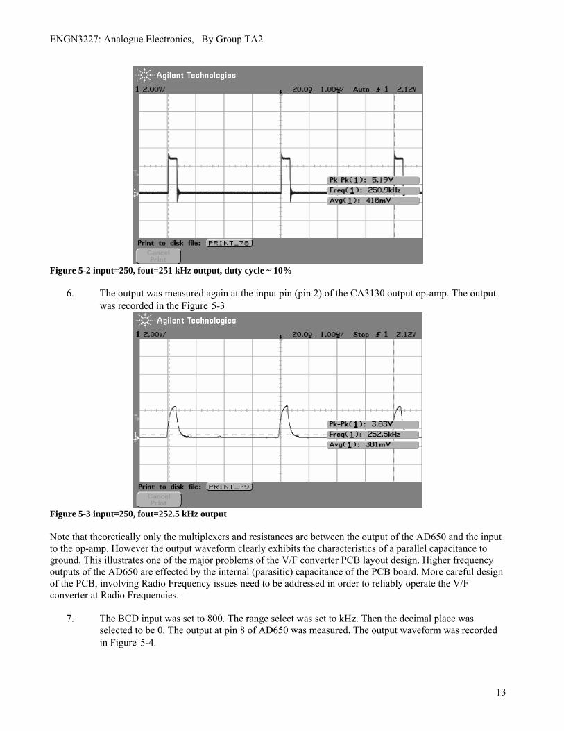
6. The output was measured again at the input pin (pin 2) of the CA3130 output op-amp. The output was recorded in the Figure 5-3
Figure 5-3 input=250, fout=252.5 kHz output Note that theoretically only the multiplexers and resistances are between the output of the AD650 and the input to the op-amp. However the output waveform clearly exhibits the characteristics of a parallel capacitance to ground. This illustrates one of the major problems of the V/F converter PCB layout design. Higher frequency outputs of the AD650 are effected by the internal (parasitic) capacitance of the PCB board. More careful design of the PCB, involving Radio Frequency issues need to be addressed in order to reliably operate the V/F converter at Radio Frequencies.
7. The BCD input was set to 800. The range select was set to kHz. Then the decimal place was
selected to be 0. The output at pin 8 of AD650 was measured. The output waveform was recorded in Figure 5-4.
13

ENGN3227: Analogue Electronics, By Group TA2
Figure 5-4 input=800, fout=830 kHz output Notice that the measured output frequency was inaccurate by a factor of 30 kHz. Thus this is outside the practical operating range of the V/F converter. This effect could be attributed to the 400kHz noise component in the AD650 input which may result in significant frequency offset at frequencies close to 400kHz. By further experimentation we were able to find that the output of the AD650 became non-linear at frequencies higher than 500 kHz. Therefore the practical operating range of the V/F converter was measured to be < 500 kHz. Our experimental results showed that for frequencies less than 500kHz the V/F converter output was accurate to within 2x(least significant figure). i.e. for the kHz range-2 kHz, for 0.1kHz range - 0.2kHz, 1Hz range - 2Hz, etc. One of the other main issues present was the lack of reliability of the PCB for high frequencies due to RF effects. One good example was the resistor present at the output of the frequency dividers, on the frequency divider side, the wave was square with minimal distortion. However, on the other side of the resistor a sawtooth waveform was observed. This suggests that our resistors act as capacitors as well as resistors for higher frequencies (around a few hundred KHz). To provide more reliable VCO function in this respect, the PCB needs to be redesigned taking into account RF design methodology. This would include concepts such as a ground plane in the board, and greater care with the width and lengths of tracks.
6 Conclusion The practical output of the AD650, after testing the PCBs was found to be less than 500 kHz. The original design requirement was that the AD650 operate up to a range of 1MHz. Factors which are likely to have caused this shift in performance are a 400 kHz noise component on the AD650 input, and that the AD650 became non-linear for frequencies above 500 kHz. At the bread boarding phase, the results closely matched the design requirements, so this shift in performance does not suggest a major flaw in the circuit design. Rather, it suggests a problem with the PCB implementation and that not all factors were considered when designing the PCBs. Such factors include RF design methodology. Regardless of this set back, the PCB implementation still operates up to the mentioned range, and clearly demonstrates the voltage to frequency conversion process.
14
ENGN3227: Analogue Electronics, By Group TA2
15
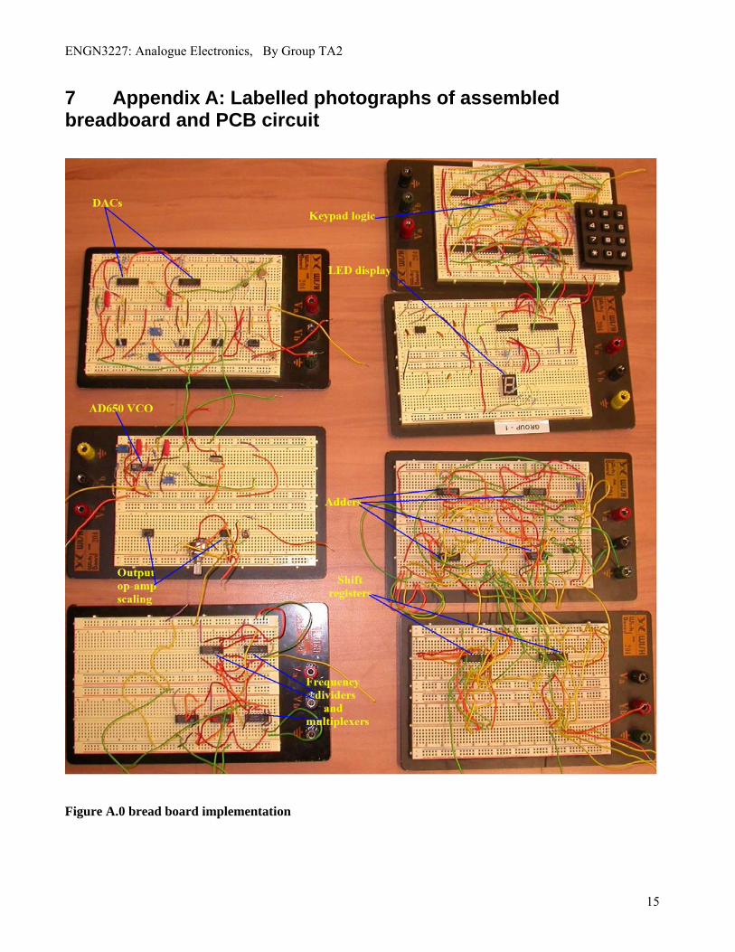
7 Appendix A: Labelled photographs of assembled breadboard and PCB circuit Figure A.0 bread board implementation
ENGN3227: Analogue Electronics, By Group TA2
16
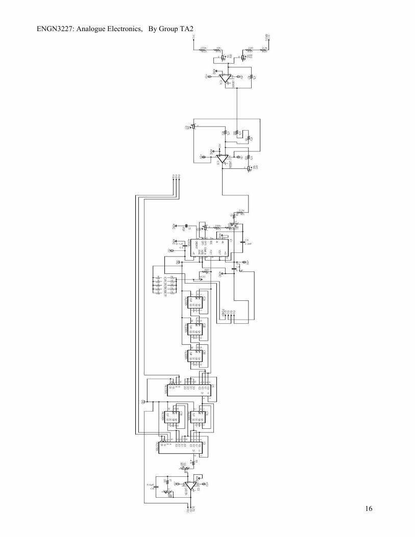
ENGN3227: Analogue Electronics, By Group TA2 Figure A.1 V/F converter schematic
Figure A.2 DAC output stage schematic
17

ENGN3227: Analogue Electronics, By Group TA2
Figure A.3 Interface schematic
18

ENGN3227: Analogue Electronics, By Group TA2
Figure A.4 AD650 PCB Layout
19
ENGN3227: Analogue Electronics, By Group TA2
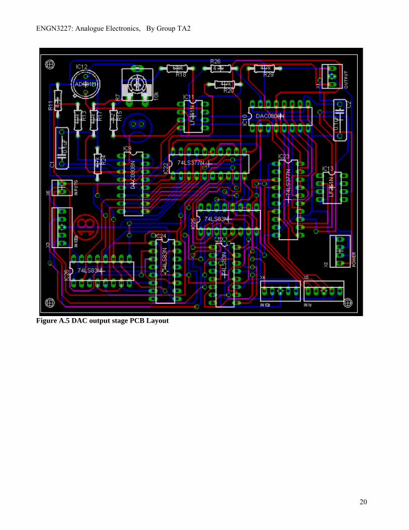
Figure A.5 DAC output stage PCB Layout
20
ENGN3227: Analogue Electronics, By Group TA2
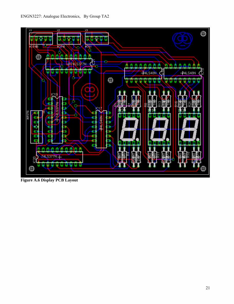
Figure A.6 Display PCB Layout
21

ENGN3227: Analogue Electronics, By Group TA2
8 Appendix B: Pspice Implementation
8.1 AD650 The simplified V/F converter of Figure 2-5 was simulated in Pspice. The major difficulty in implementation of the circuit is the two state switch. This is particularly difficult to implement due to the fact that it is switching a current source between. The other issue is that the output range of the simplified V/F converter will not be able to perform to the specifications of the AD650, due to slew rate limitations of op-amps and the inefficient switch implementation (switching transients). For this reason a circuit similar to the one of Figure 2-5 was implemented, but calibrated to output from 1-999 Hz. A schematic of the implemented AD650 is given in the
Figure 8-1 AD650 Implementation The circuit was tested with a full scale input of 999. The output waveform is shown in the Figure 8-2. The measured frequency was 1.002kHz.
22

ENGN3227: Analogue Electronics, By Group TA2
Figure 8-2 AD650 output waveform The circuit used for testing the AD605 is given in Figure 8-3
Figure 8-3
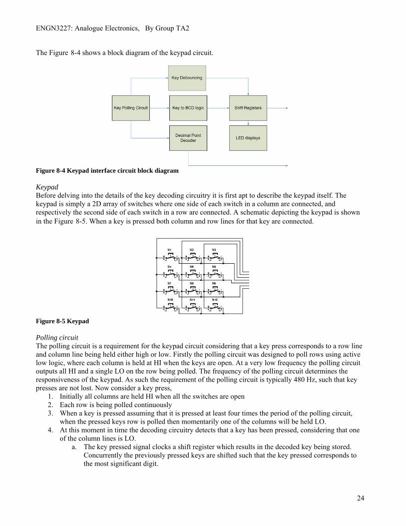
8.2 Keypad The keypad interface circuit was designed using a 4x3 keypad shown below. The ‘*’ key represents the decimal point, and the ‘#’ was designated as the ‘OK’ key pressed. A switch was used specify the range select for the output which can be either be Hz or KHz. To specify a frequency the user presses three digits with an optional decimal point press, and selects the appropriate range, finally the ‘OK’ key is pressed. The pressed digits would be recorded on three 7-segment LED’s which would also display the decimal point. The design of the keypad can be classified into a number of sub modules,
• A keypad polling circuit which polls either the rows or columns of the keypad • The digit key presses need to be decoded using key to BCD logic • Key de-bouncing circuit to ensure that digit presses are stored properly • Shift registers to store key presses • The decimal point key press needs to be decoded using state logic • The BCD to LED converters and the LEDs
23
ENGN3227: Analogue Electronics, By Group TA2
The Figure 8-4 shows a block diagram of the keypad circuit.
Figure 8-4 Keypad interface circuit block diagram Keypad Before delving into the details of the key decoding circuitry it is first apt to describe the keypad itself. The keypad is simply a 2D array of switches where one side of each switch in a column are connected, and respectively the second side of each switch in a row are connected. A schematic depicting the keypad is shown in the Figure 8-5. When a key is pressed both column and row lines for that key are connected.
Figure 8-5 Keypad Polling circuit The polling circuit is a requirement for the keypad circuit considering that a key press corresponds to a row line and column line being held either high or low. Firstly the polling circuit was designed to poll rows using active low logic, where each column is held at HI when the keys are open. At a very low frequency the polling circuit outputs all HI and a single LO on the row being polled. The frequency of the polling circuit determines the responsiveness of the keypad. As such the requirement of the polling circuit is typically 480 Hz, such that key presses are not lost. Now consider a key press,
1. Initially all columns are held HI when all the switches are open 2. Each row is being polled continuously 3. When a key is pressed assuming that it is pressed at least four times the period of the polling circuit,
when the pressed keys row is polled then momentarily one of the columns will be held LO. 4. At this moment in time the decoding circuitry detects that a key has been pressed, considering that one
of the column lines is LO. a. The key pressed signal clocks a shift register which results in the decoded key being stored.
Concurrently the previously pressed keys are shifted such that the key pressed corresponds to the most significant digit.
24

ENGN3227: Analogue Electronics, By Group TA2
25
b. The digits stored in the three shift registers as decoded concurrently in part 5 are displayed on three LEDs.
5. Concurrently one column and one row will be held LO. a. The Key can be decoded based on which column and row lines are LO b. If the key pressed was decimal point
i. Decimal point decoder logic is used, to determine the decimal place within the 3 digit input (1 or 2).
c. Else if the key pressed was OK i. When the ‘OK’ key is pressed the DAC input shift registers are clocked
Else ii. Convert row,column lines to BCD using the following Logic table 011 101 110 0111 0001 0010 0011 1011 0100 0101 0110 1101 0111 1000 1001 1110 0000 The decimal digit is stored in a shift register as in step 4 a.
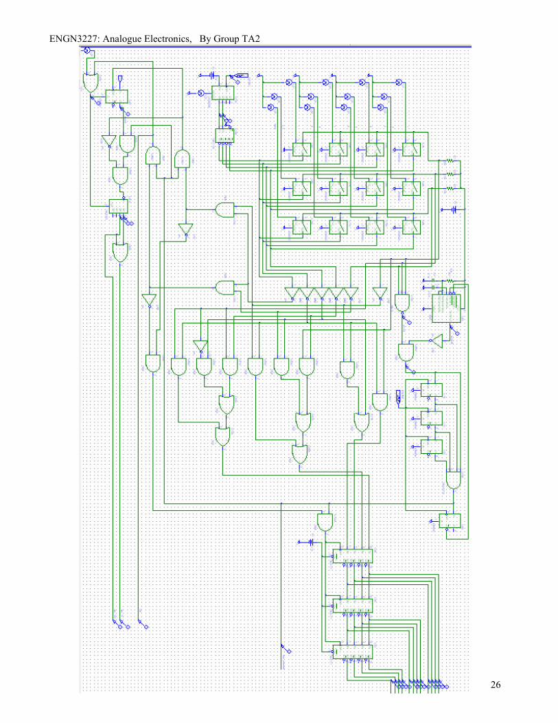
The Pspice schematic of the described keypad interface is given in the
ENGN3227: Analogue Electronics, By Group TA2
26

ENGN3227: Analogue Electronics, By Group TA2 Figure 8-6 Pspice keypad implementation
27
ENGN3227: Analogue Electronics, By Group TA2
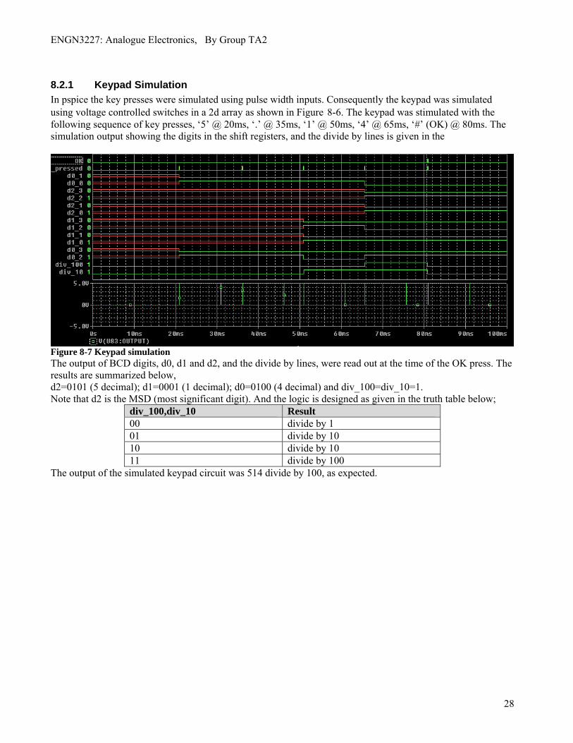
8.2.1 Keypad Simulation In pspice the key presses were simulated using pulse width inputs. Consequently the keypad was simulated using voltage controlled switches in a 2d array as shown in Figure 8-6. The keypad was stimulated with the following sequence of key presses, ‘5’ @ 20ms, ‘.’ @ 35ms, ‘1’ @ 50ms, ‘4’ @ 65ms, ‘#’ (OK) @ 80ms. The simulation output showing the digits in the shift registers, and the divide by lines is given in the
Figure 8-7 Keypad simulation The output of BCD digits, d0, d1 and d2, and the divide by lines, were read out at the time of the OK press. The results are summarized below, d2=0101 (5 decimal); d1=0001 (1 decimal); d0=0100 (4 decimal) and div_100=div_10=1. Note that d2 is the MSD (most significant digit). And the logic is designed as given in the truth table below;
div_100,div_10 Result 00 divide by 1 01 divide by 10 10 divide by 10 11 divide by 100
The output of the simulated keypad circuit was 514 divide by 100, as expected.
28