Embed Size (px)
Citation preview
©20
12 N
atu
re A
mer
ica,
Inc.
All
rig
hts
res
erve
d.
protocol
nature protocols | VOL.7 NO.2 | 2012 | 311
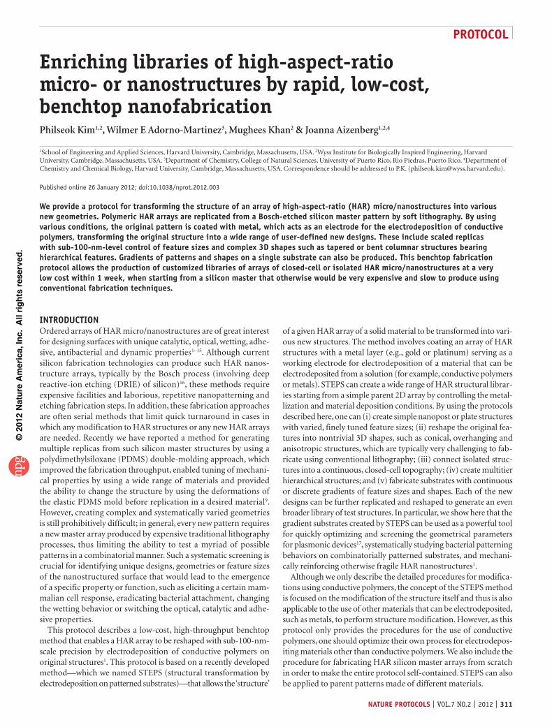
IntroDuctIonOrdered arrays of HAR micro/nanostructures are of great interest for designing surfaces with unique catalytic, optical, wetting, adhe-sive, antibacterial and dynamic properties1–15. Although current silicon fabrication technologies can produce such HAR nanos-tructure arrays, typically by the Bosch process (involving deep reactive-ion etching (DRIE) of silicon)16, these methods require expensive facilities and laborious, repetitive nanopatterning and etching fabrication steps. In addition, these fabrication approaches are often serial methods that limit quick turnaround in cases in which any modification to HAR structures or any new HAR arrays are needed. Recently we have reported a method for generating multiple replicas from such silicon master structures by using a polydimethylsiloxane (PDMS) double-molding approach, which improved the fabrication throughput, enabled tuning of mechani-cal properties by using a wide range of materials and provided the ability to change the structure by using the deformations of the elastic PDMS mold before replication in a desired material9. However, creating complex and systematically varied geometries is still prohibitively difficult; in general, every new pattern requires a new master array produced by expensive traditional lithography processes, thus limiting the ability to test a myriad of possible patterns in a combinatorial manner. Such a systematic screening is crucial for identifying unique designs, geometries or feature sizes of the nanostructured surface that would lead to the emergence of a specific property or function, such as eliciting a certain mam-malian cell response, eradicating bacterial attachment, changing the wetting behavior or switching the optical, catalytic and adhe-sive properties.
This protocol describes a low-cost, high-throughput benchtop method that enables a HAR array to be reshaped with sub-100-nm- scale precision by electrodeposition of conductive polymers on original structures1. This protocol is based on a recently developed method—which we named STEPS (structural transformation by electrodeposition on patterned substrates)—that allows the ‘structure’
of a given HAR array of a solid material to be transformed into vari-ous new structures. The method involves coating an array of HAR structures with a metal layer (e.g., gold or platinum) serving as a working electrode for electrodeposition of a material that can be electrodeposited from a solution (for example, conductive polymers or metals). STEPS can create a wide range of HAR structural librar-ies starting from a simple parent 2D array by controlling the metal-lization and material deposition conditions. By using the protocols described here, one can (i) create simple nanopost or plate structures with varied, finely tuned feature sizes; (ii) reshape the original fea-tures into nontrivial 3D shapes, such as conical, overhanging and anisotropic structures, which are typically very challenging to fab-ricate using conventional lithography; (iii) connect isolated struc-tures into a continuous, closed-cell topography; (iv) create multitier hierarchical structures; and (v) fabricate substrates with continuous or discrete gradients of feature sizes and shapes. Each of the new designs can be further replicated and reshaped to generate an even broader library of test structures. In particular, we show here that the gradient substrates created by STEPS can be used as a powerful tool for quickly optimizing and screening the geometrical parameters for plasmonic devices17, systematically studying bacterial patterning behaviors on combinatorially patterned substrates, and mechani-cally reinforcing otherwise fragile HAR nanostructures1.
Although we only describe the detailed procedures for modifica-tions using conductive polymers, the concept of the STEPS method is focused on the modification of the structure itself and thus is also applicable to the use of other materials that can be electrodeposited, such as metals, to perform structure modification. However, as this protocol only provides the procedures for the use of conductive polymers, one should optimize their own process for electrodepos-iting materials other than conductive polymers. We also include the procedure for fabricating HAR silicon master arrays from scratch in order to make the entire protocol self-contained. STEPS can also be applied to parent patterns made of different materials.
Enriching libraries of high-aspect-ratio micro- or nanostructures by rapid, low-cost, benchtop nanofabricationPhilseok Kim1,2, Wilmer E Adorno-Martinez3, Mughees Khan2 & Joanna Aizenberg1,2,4
1School of Engineering and Applied Sciences, Harvard University, Cambridge, Massachusetts, USA. 2Wyss Institute for Biologically Inspired Engineering, Harvard University, Cambridge, Massachusetts, USA. 3Department of Chemistry, College of Natural Sciences, University of Puerto Rico, Rio Piedras, Puerto Rico. 4Department of Chemistry and Chemical Biology, Harvard University, Cambridge, Massachusetts, USA. Correspondence should be addressed to P.K. ([email protected]).
Published online 26 January 2012; doi:10.1038/nprot.2012.003
We provide a protocol for transforming the structure of an array of high-aspect-ratio (Har) micro/nanostructures into various new geometries. polymeric Har arrays are replicated from a Bosch-etched silicon master pattern by soft lithography. By using various conditions, the original pattern is coated with metal, which acts as an electrode for the electrodeposition of conductive polymers, transforming the original structure into a wide range of user-defined new designs. these include scaled replicas with sub-100-nm-level control of feature sizes and complex 3D shapes such as tapered or bent columnar structures bearing hierarchical features. Gradients of patterns and shapes on a single substrate can also be produced. this benchtop fabrication protocol allows the production of customized libraries of arrays of closed-cell or isolated Har micro/nanostructures at a very low cost within 1 week, when starting from a silicon master that otherwise would be very expensive and slow to produce using conventional fabrication techniques.
©20
12 N
atu
re A
mer
ica,
Inc.
All
rig
hts
res
erve
d.
protocol
312 | VOL.7 NO.2 | 2012 | nature protocols
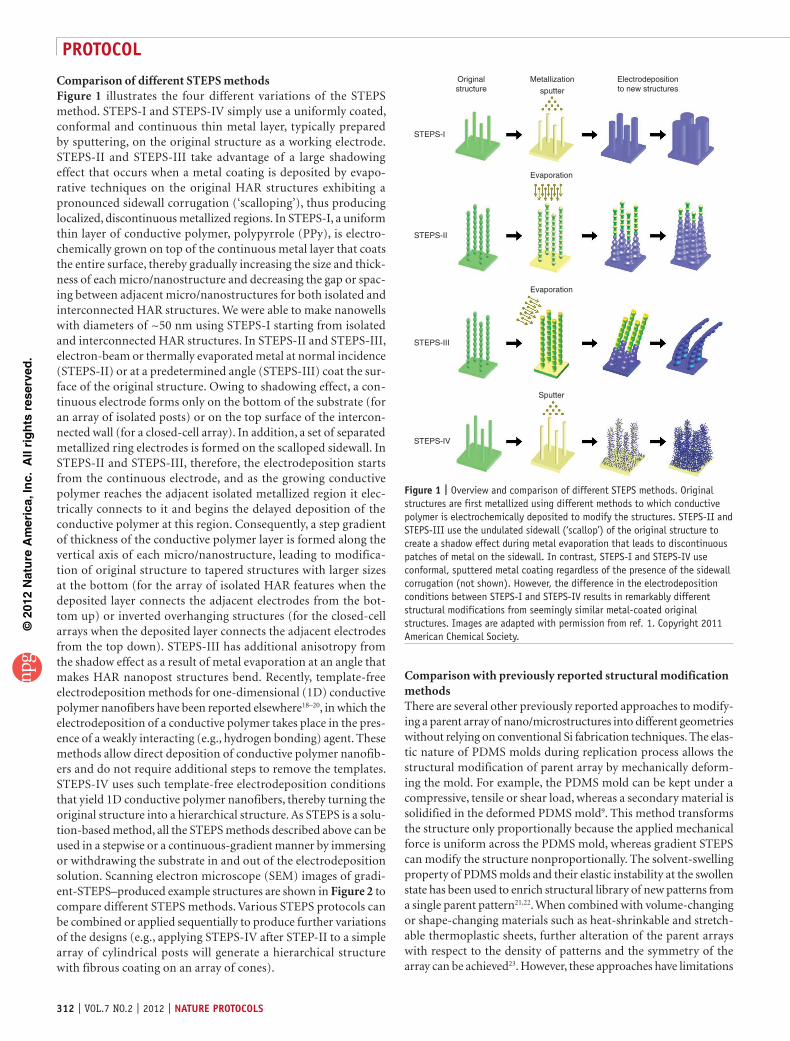
Comparison of different STEPS methodsFigure 1 illustrates the four different variations of the STEPS method. STEPS-I and STEPS-IV simply use a uniformly coated, conformal and continuous thin metal layer, typically prepared by sputtering, on the original structure as a working electrode. STEPS-II and STEPS-III take advantage of a large shadowing effect that occurs when a metal coating is deposited by evapo-rative techniques on the original HAR structures exhibiting a pronounced sidewall corrugation (‘scalloping’), thus producing localized, discontinuous metallized regions. In STEPS-I, a uniform thin layer of conductive polymer, polypyrrole (PPy), is electro-chemically grown on top of the continuous metal layer that coats the entire surface, thereby gradually increasing the size and thick-ness of each micro/nanostructure and decreasing the gap or spac-ing between adjacent micro/nanostructures for both isolated and interconnected HAR structures. We were able to make nanowells with diameters of ~50 nm using STEPS-I starting from isolated and interconnected HAR structures. In STEPS-II and STEPS-III, electron-beam or thermally evaporated metal at normal incidence (STEPS-II) or at a predetermined angle (STEPS-III) coat the sur-face of the original structure. Owing to shadowing effect, a con-tinuous electrode forms only on the bottom of the substrate (for an array of isolated posts) or on the top surface of the intercon-nected wall (for a closed-cell array). In addition, a set of separated metallized ring electrodes is formed on the scalloped sidewall. In STEPS-II and STEPS-III, therefore, the electrodeposition starts from the continuous electrode, and as the growing conductive polymer reaches the adjacent isolated metallized region it elec-trically connects to it and begins the delayed deposition of the conductive polymer at this region. Consequently, a step gradient of thickness of the conductive polymer layer is formed along the vertical axis of each micro/nanostructure, leading to modifica-tion of original structure to tapered structures with larger sizes at the bottom (for the array of isolated HAR features when the deposited layer connects the adjacent electrodes from the bot-tom up) or inverted overhanging structures (for the closed-cell arrays when the deposited layer connects the adjacent electrodes from the top down). STEPS-III has additional anisotropy from the shadow effect as a result of metal evaporation at an angle that makes HAR nanopost structures bend. Recently, template-free electrodeposition methods for one-dimensional (1D) conductive polymer nanofibers have been reported elsewhere18–20, in which the electrodeposition of a conductive polymer takes place in the pres-ence of a weakly interacting (e.g., hydrogen bonding) agent. These methods allow direct deposition of conductive polymer nanofib-ers and do not require additional steps to remove the templates. STEPS-IV uses such template-free electrodeposition conditions that yield 1D conductive polymer nanofibers, thereby turning the original structure into a hierarchical structure. As STEPS is a solu-tion-based method, all the STEPS methods described above can be used in a stepwise or a continuous-gradient manner by immersing or withdrawing the substrate in and out of the electrodeposition solution. Scanning electron microscope (SEM) images of gradi-ent-STEPS–produced example structures are shown in Figure 2 to compare different STEPS methods. Various STEPS protocols can be combined or applied sequentially to produce further variations of the designs (e.g., applying STEPS-IV after STEP-II to a simple array of cylindrical posts will generate a hierarchical structure with fibrous coating on an array of cones).
Comparison with previously reported structural modification methodsThere are several other previously reported approaches to modify-ing a parent array of nano/microstructures into different geometries without relying on conventional Si fabrication techniques. The elas-tic nature of PDMS molds during replication process allows the structural modification of parent array by mechanically deform-ing the mold. For example, the PDMS mold can be kept under a compressive, tensile or shear load, whereas a secondary material is solidified in the deformed PDMS mold9. This method transforms the structure only proportionally because the applied mechanical force is uniform across the PDMS mold, whereas gradient STEPS can modify the structure nonproportionally. The solvent-swelling property of PDMS molds and their elastic instability at the swollen state has been used to enrich structural library of new patterns from a single parent pattern21,22. When combined with volume-changing or shape-changing materials such as heat-shrinkable and stretch-able thermoplastic sheets, further alteration of the parent arrays with respect to the density of patterns and the symmetry of the array can be achieved23. However, these approaches have limitations
Originalstructure
Metallization Electrodepositionto new structuressputter
Sputter
Evaporation
Evaporation
STEPS-I
STEPS-II
STEPS-III
STEPS-IV
Figure 1 | Overview and comparison of different STEPS methods. Original structures are first metallized using different methods to which conductive polymer is electrochemically deposited to modify the structures. STEPS-II and STEPS-III use the undulated sidewall (‘scallop’) of the original structure to create a shadow effect during metal evaporation that leads to discontinuous patches of metal on the sidewall. In contrast, STEPS-I and STEPS-IV use conformal, sputtered metal coating regardless of the presence of the sidewall corrugation (not shown). However, the difference in the electrodeposition conditions between STEPS-I and STEPS-IV results in remarkably different structural modifications from seemingly similar metal-coated original structures. Images are adapted with permission from ref. 1. Copyright 2011 American Chemical Society.
©20
12 N
atu
re A
mer
ica,
Inc.
All
rig
hts
res
erve
d.
protocol
nature protocols | VOL.7 NO.2 | 2012 | 313
in their application to HAR structures; they are typically limited to proportional transformation of the original shape or are limited by loss in fidelity of the patterns upon modification. STEPS is particu-larly advantageous compared with any earlier reported approaches because of its unique gradient modification option that allows the fabrication of substrates bearing a set of slightly different 3D shapes of a sort. These gradient-STEPS–generated substrates are especially useful for systematic studies of structure-property relations and for fast screening of multiple geometrical parameters associated with various surface properties. In addition, none of these previously reported methods allows the nonproportional modification and vertical changes of the geometry of the original features, thus lead-ing to the fabrication of complex 3D structures such as hierarchical, tapered and overhanging structures. Nevertheless, these previously reported methods offer complementary structural modification capabilities, and thus the combinations of these methods with STEPS would provide a wider range of options for transforming a parent array structure.
Exemplary applications of STEPS-modified HAR arraysAlthough a broad range of applications can be envisioned for the surfaces that bear user-defined, arbitrarily shaped HAR struc-tures, we present here our preliminary data from using these sur-faces for control of wetting, ice formation, mechanical and optical properties as well as as a substrate for biological studies4,5,8,9,17. We also emphasize that using the electroactive behavior of the conductive polymer layer created during STEPS modification will open a completely new avenue for creating dynamically actuated HAR structures6.
Fine tuning of wetting properties. Closely packed, ordered micro- or nanopost arrays have unique wetting properties when combined with appropriate surface chemistry24. Structural modification of HAR arrays using STEPS can provide precisely controlled diam-eters of micropost and the associated surface-filling ratio (phi ratio) to systematically study their effect on the wetting behavior. In particular, surfaces with overhanging features and hierarchical length scales in surface roughness are reported to show improved superhydrophobicity or oleophobicity, as well as pressure-stable superhydrophobicity2,13. These overhanging features or hierarchi-cal structures can be easily produced by STEPS-II on closed-cell HAR arrays or by STEPS-IV process on any of the HAR arrays to add additional nanoscale roughness. Unidirectionally tilted micro/nanopost array structures have been reported to exhibit anisotropic wetting and adhesive properties3,25,26. STEPS-III modi-fication allows fine tuning of the tilting angle and the diameter of the posts for investigating directional wetting behaviors in further detail. Moreover, combinations of different STEPS processes will lead to hierarchical nanoscale architectures that can potentially lead to unforeseen new wetting properties. For example, a simple HAR nanopost array was transformed to unidirectionally bent, hierar-chical structures by combining STEPS-III and STEPS-IV processes for which the study of the wetting characteristics are underway (Supplementary Fig. 1).
Mechanical reinforcement of nanostructures. The poor mechani-cal stability of HAR micro/nanostructures often leads to structural failures such as breaking, lateral or vertical collapse and cluster-ing, which are detrimental to their functions and make them
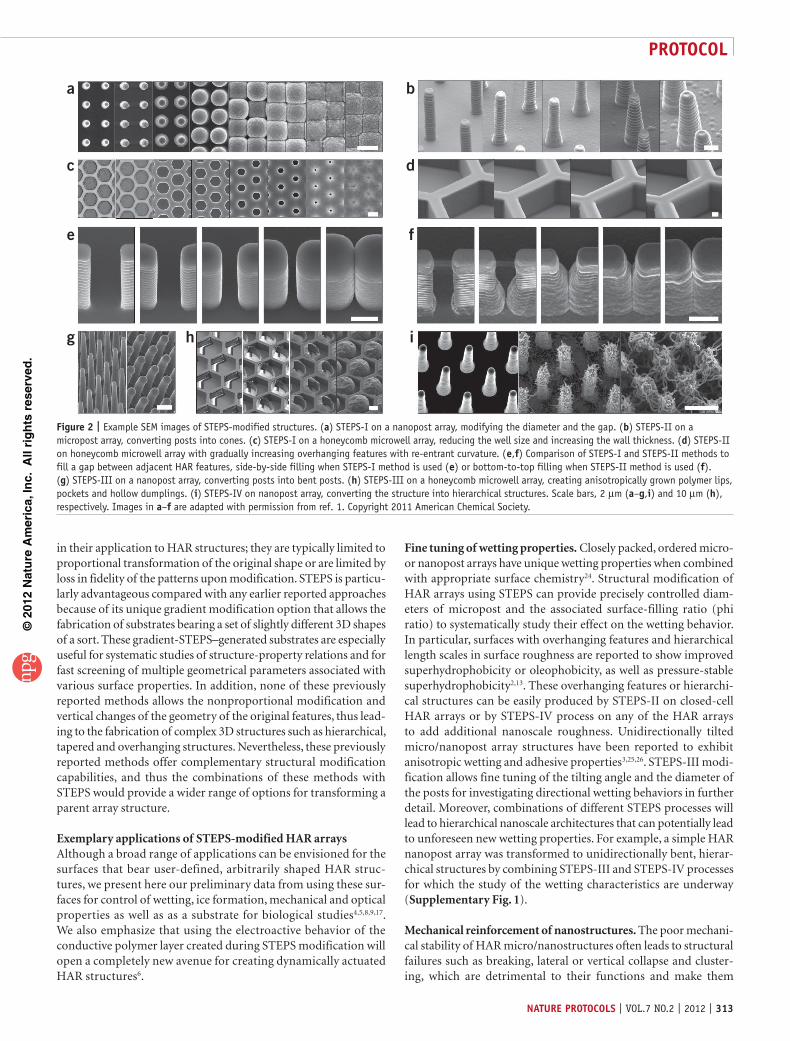
Figure 2 | Example SEM images of STEPS-modified structures. (a) STEPS-I on a nanopost array, modifying the diameter and the gap. (b) STEPS-II on a micropost array, converting posts into cones. (c) STEPS-I on a honeycomb microwell array, reducing the well size and increasing the wall thickness. (d) STEPS-II on honeycomb microwell array with gradually increasing overhanging features with re-entrant curvature. (e,f) Comparison of STEPS-I and STEPS-II methods to fill a gap between adjacent HAR features, side-by-side filling when STEPS-I method is used (e) or bottom-to-top filling when STEPS-II method is used (f). (g) STEPS-III on a nanopost array, converting posts into bent posts. (h) STEPS-III on a honeycomb microwell array, creating anisotropically grown polymer lips, pockets and hollow dumplings. (i) STEPS-IV on nanopost array, converting the structure into hierarchical structures. Scale bars, 2 µm (a–g,i) and 10 µm (h), respectively. Images in a–f are adapted with permission from ref. 1. Copyright 2011 American Chemical Society.
a
c
e
g h i
f
d
b
©20
12 N
atu
re A
mer
ica,
Inc.
All
rig
hts
res
erve
d.
protocol
314 | VOL.7 NO.2 | 2012 | nature protocols
often impractical in real technologies. STEPS can provide a simple means to create mechanically reinforced and robust nanostruc-tures through either uniform conformal coating of HAR structures (STEPS-I) or controlled increase of their basal size (STEPS-II). For example, an array of Y-shaped HAR epoxy microcolumns that already show improved mechanical stability over an array of simple cylindrical posts was further strengthened when transformed to a tapered structure by STEPS-II protocol. The increased mechani-cal stability of such structures was confirmed by nanoindenta-tion experiments, as well as by finite element method simulations (Supplementary Fig. 2)1. The tapered HAR microstructure showed a twofold decrease in the maximum induced stresses compared with that of the original microstructure.
Tuning the plasmonic properties. Nanoskiving is a form of edge lithography in which thin slices from a block of composite mate-rial with embedded topographical patterns of choice are gener-ated by sectioning with a microtome to generate multiple copies of indistinguishable nanostructures27. STEPS-I modification of a nanopost array yields a conductive polymer-coated nanopost array, which then can be covered by a second layer of metal and used for nanoskiving to produce sophisticated plasmonic nanostruc-tures, such as highly ordered periodic arrays of metallic concentric rings (ring resonators)17. Such highly ordered and closely spaced nanoscale concentric metallic ring arrays are very challenging to fabricate by existing lithographic techniques or basic nanoskiving approaches. These array structures have double localized surface plasmon resonances and are useful for ultrasensitive surface-enhanced Raman scattering sensors because of a large local field enhancement effect. The gap between the inner and the outer gold nanorings can be quickly optimized by running a gradient–STEPS-I protocol. Fabrication of other periodic arrays of heterogeneous concentric rings and counter-facing concentric C-ring (split ring resonators) arrays can also be simplified considerably by using the STEPS method.
Controlling the attachment of biological cells. The effects of topography and mechanical properties of surfaces on mammalian cell behavior, bacterial adhesion and biofilm formation have only recently been explored but remain largely unknown4,28–31. Ordered micro- or nanopatterned arrays with systematically changing fea-tures are an excellent platform for understanding these effects and identifying crucial feature sizes, length scales or shapes of surface structures that elicit programmable cell behaviors (differentia-tion, adhesion, proliferation, death and so on). Such surfaces may provide an efficient and predictable means to inhibit the attach-ment of bacterial cells, an integral step for biofilm formation11. The bacterial assembly can also be markedly affected by the under-lying topography, which may be crucial in the removal of bacterial biofilms by mechanical force. Gradient-STEPS modification of an existing simple master pattern can provide a unique combinatorial substrate to screen a wide range of topographical cues that influ-ence the arrangement of cells and bacteria and their subsequent behaviors32. For example, about 250 different patterned regions can be created on a 2 cm × 1.5 cm substrate for a systematic and combinatorial study1. Moreover, the gradient-STEPS–modified substrate, once created, can serve as a new master for making nega-tive molds and further producing replica substrates in different materials and with varying stiffness. We have shown that there exist
definite, characteristic feature sizes and geometries of the underly-ing substrate that induce bacterial patterning, orientation or the complete inhibition of attachment4.
Patterned self-assembly. Evaporation-induced self-assembly of the arrays of HAR structures into complex, chiral, anisotropic and hierarchical 3D structures has been identified as a simple yet pow-erful biomimetic nanofabrication method that can create strik-ingly different and novel structures that are impossible to fabricate using conventional techniques5,10,33,34. STEPS can provide unique gradient template HAR structures to help investigators to quickly understand and determine the requirements of the generation of customized patterns created by the evaporative self-assembly process. These new patterns can be potentially useful as sensors, capture/release systems, dynamic structural colors and mechani-cally interlocking nonchemical glues.
LimitationsSTEPS can only add new material to existing structures and increase their sizes, but it cannot etch or reduce feature sizes. STEPS cannot modify the pitch of the original array structure. However, by com-bining STEPS with stretching or shearing of the PDMS mold when casting polymer replicas9, modified array structures with different periodicities and symmetries can be obtained.
STEPS-II and STEPS-III rely on the sidewall corrugation artifact from the DRIE of a Si master. Therefore, this method cannot be used for HAR arrays with smooth walls prepared using different methods.
The rate of polymerization during the STEPS process can vary when the area being modified has regions with limited diffu-sion of reactants from the electrodeposition solution. Although this feature leads to nonuniform coatings with reduced added thickness at the diffusion-limited sites, it can be creatively used to induce additional, controlled shape transformations. For example, an array of posts with circular cross-sections can be transformed into an array of octagonal columns or hexagonal columns, depending on their arrangement; in some cases, this
1 µm
a
c d
b
1 µm
10 µm 10 µm
Figure 3 | SEM images of fabricated Si masters. (a) Hexagonal array of 350 nm posts at 2 µm pitch and 3 µm height. (b) Hexagonal array of 1 µm posts at 3 µm pitch and 10 µm height. (c) Honeycomb with 1 µm wall thickness, 20 µm wall length and 15 µm height. (d) Y-shaped hexagonal columnar array with 1 µm wall thickness, 4 µm wall length, 2 µm gap and 5 µm height.
©20
12 N
atu
re A
mer
ica,
Inc.
All
rig
hts
res
erve
d.
protocol
nature protocols | VOL.7 NO.2 | 2012 | 315
can be considered to be a limitation. STEPS relies on solution-based deposition methods. This means that there is some degree of edge effect, especially at the meniscus of the electrodeposition solution at the top of the substrate. This meniscus-derived edge effect is even more pronounced during gradient-STEPS proc-esses and when a small substrate is used. Electrodeposition has certain nonuniformity, especially around the edges and corners of the substrate where the electric field and the diffusion rate of reactants can be locally inhomogeneous. This can affect the overall uniformity of STEPS-modified structures, which is more pronounced for small substrates. If a uniform and large-area substrate is needed, one should consider using a larger parent substrate to ensure that a sufficient area inside the substrate has highly uniform modified patterns.
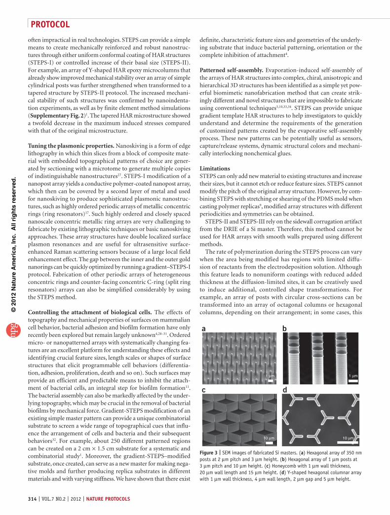
Experimental designReticle design and Si master fabrication. For the purpose of dem-onstrating the effectiveness of the STEPS technique, we fabricated four different representative uniform HAR patterns and structures (height/width ≥ 5:1) in Si substrates by using a combination of tech-niques and approaches similar to those described elsewhere28,35–38. Figure 3a,b shows exemplary hexagonal arrays of cylindrical posts (diameter of 350 nm and 1 µm; pitch of 2 and 3 µm and 8.5:1 and 10:1 aspect ratios, respectively) that were used to describe applications
of STEPS-I, STEPS-II, STEPS-III and STEPS-IV. Figure 3c shows an exemplary closed-cell honeycomb Si master (aspect ratio of 15:1) that was used as a STEPS-I demonstration. Figure 3d shows an open-cell, regularly disrupted honeycomb array (aspect ratio of 5:1) that was used to demonstrate STEPS-II. Projection lithography was performed using a Nikon ×5 i-line stepper in order to achieve submicron resolution across large areas (full 100 or 150 mm wafer) with minimum feature sizes ranging from < 500 nm to 1 µm. The use of an i-line stepper required making a 6 in × 0.25 in quartz mask or reticle. Pattern generation and layout design for the reticles were performed using L-edit, a commercial layout editor (Tanner EDA). Details of in-house reticle fabrication and commercial mask shops have been provided in the PROCEDURE section. The large-scale patterning with projection lithography was followed by a repeti-tive etching procedure using a Bosch advanced silicon etch39 in an STS DRIE tool to produce HAR structures with controlled height. The Bosch process16,40,41, which cycles between an isotropic plasma Si etch step and a passivation step, results in near-vertical, anisotropic Si columnar profiles at relatively high Si etch rates. Sidewall corruga-tion of the Si masters, commonly known as scallops, are an artifact of this cycling between an etch step and a passivation step (Fig. 3a,b). These scallops are also replicated in molding and casting procedure and are responsible for the formation of isolated, stepped electrodes, which are crucial for STEPS-II and STEPS-III.
MaterIalsREAGENTS
CR 14 chrome etchant (Cyantek Corporation) ! cautIon It is corrosive and irritating to the eyes, skin and respiratory system. Wear proper personal protective equipment (PPE) and handle it inside an acid hood.Hexamethyldisilazane (HMDS, reagent grade, ≥99%; Sigma-Aldrich, cat. no. 440791, CAS 999-97-3) ! cautIon HMDS is flammable. Also avoid skin contact and inhalation, as it will cause irritation and burns; it has a strong odor as well. Wear proper PPE and handle it in a fume hood.Megaposit SPR 700-1.0 series i-line photoresist (Microchem) ! cautIon It is a combustible liquid; handle with care. Contact with eyes and skin can cause irritation. Avoid inhaling vapors or mist, and handle it in a proper fume hood. Wear goggles, gloves and protective clothing.Microposit MF CD 26, 0.26N, surfactant-free (Shipley Company, Microchem) ! cautIon It is an alkaline-based corrosive liquid containing tetramethyl ammonium hydroxide. It is an irritant; avoid contact with eyes, skin and clothing and handle it in a ventilated area. Wear gloves, goggles and protective clothing.Deionized (DI) waterHydrogen peroxide (H
2O
2, 30–32% (wt/vol); VWR, cat. no. JT2186-3, CAS
7722-84-1) ! cautIon It is corrosive and a strong oxidizing agent. Handle it in an acid fume hood and wear proper PPE (face shield, acid gloves and apron).Sulfuric acid (H
2SO
4, 93% (wt/vol); VWR, cat. no. JT6902-5, CAS
7664-93-9) ! cautIon It is highly corrosive; handle it in an acid fume hood and wear proper PPE (face shield, acid gloves and apron).Sodium dodecylbenzene sulfonate (SDBS, technical grade; Sigma- Aldrich, cat. no. 289957) or (88% technical grade; Acros Organics, cat. no. 325910010, CAS 25155-30-0) ! cautIon SDBS is an irritant. Do not breathe the vapor.Lithium perchlorate (LiClO
4, 99.99% trace metals basis; Sigma-Aldrich,
cat. no. 431567; CAS 7791-03-9) ! cautIon LiClO4 is a strong oxidizer.
Contact with combustible material may cause fire. Avoid contact with organic materials, combustible materials and strong reducing agents.Sodium phosphate monobasic monohydrate (NaH
2PO
4·H
2O, ACS reagent
grade, 98.0–102.0%; Sigma-Aldrich, cat. no. S9638, CAS 10049-21-5)Sodium phosphate dibasic heptahydrate (Na
2HPO
4·7H
2O, ACS reagent
grade, 98.0–102.0%; Sigma-Aldrich, cat. no. S9390, CAS 7782-85-6)
•
•
•
•
••
•
•
•
•
•
Aluminum oxide, activated, weakly acidic, Brockmann I, ~150 mesh, 58 Å (surface area 155 m2 g − 1; Sigma-Aldrich, cat. no. 267740, or CAMAG 506-C-I, CAS 1344-28-1) ! cautIon Work in a well-ventilated area. Use a dust mask.Pyrrole (reagent grade, 98%; Sigma-Aldrich, cat. no. 131709, CAS 109-97-7) ! cautIon Pyrrole is corrosive, irritating and flammable. Wear appropriate PPE such as gloves, a lab coat, and eye and face protection.Single-component UV-curable epoxy resin (UVO-114, single component; Epoxy Technology, PB068145) ! cautIon This material is light sensitive and should be kept in a dark and cool area.Platinum gauze (100 mesh woven, 99.9% metal basis; Alfa Aesar, cat. no. 10282, CAS 7440-06-4)Gold surface cleaning solution (Sigma-Aldrich, cat. no. 667978)Silicon waferHeptadecafluoro-1,1,2,2-tetrahydrodecyl trichlorosilane (F17-silane; Gelest, cat. no. SIH5841.0, CAS 78560-44-8) ! cautIon F17-silane is corrosive and moisture-sensitive. Use appropriate PPE and handle it in a dry box.Sylgard 184 kit (Dow)
EQUIPMENTBlank photomask, Cr on quartz plate (6 in × 0.25 in, precoated with AZ1518 photoresist; Nanofilm Microcircuit Technology)Direct laser writing system (Heidelberg, DWL 66)Vapor prime vacuum oven (Yield Engineering Systems, ES LP-III)Cold plateSpin coater (SSI 150) crItIcal Make sure to use a spinner with a lid to minimize spin resist thickness variation due to air turbulence while spinning a wafer.Hot plateStepper (×5, Nikon, NSR-2005i9)Inspection microscope (Nikon, OPTIPHOT 88)Plasma asher (Matrix 106)Oxide dry etcher (AME 5000)Inductively coupled plasma (ICP) DRIE system (Surface Technology Systems)Veeco profilometer (Dektak 6M, Veeco)Field emission scanning electron microscope (Zeiss, SUPRA 40 or Ultra 55)Disposable plastic syringes free from latex and silicone oil (~3 ml)
•
•
•
•
•••
•
•
••••
••••••
•••
©20
12 N
atu
re A
mer
ica,
Inc.
All
rig
hts
res
erve
d.
protocol
316 | VOL.7 NO.2 | 2012 | nature protocols
Nylon membrane syringe filters with 0.45-µm pore sizeSilver/silver chloride (Ag/AgCl) reference electrode, saturated with NaCl (BASi, cat. no. MF-2052 or MF-2078 or MF-2079)Potentiostat/galvanostat (Princeton Applied Research, VersaSTAT3-200) and software (Princeton Applied Research, Versastudio version V2.03.4182 or higher; http://www.princetonappliedresearch.com/Downloads/Index.aspx)Stir plate (VWR, Lab Disc S41, cat. no. 97056-526 or equivalent)Stir barSyringe pump (World Precision Instrument, model no. UMP3)Electrical contact (e.g., alligator clips, copper wire, silver conductive paste)Probe sonicator (Branson, Digital Sonifier, model no. S-450D or equivalent)e-beam evaporator (Denton Vacuum, EE-4 Physical Vapor Deposition System)Custom-made tilting stageDesktop sputter coater (Denton Vacuum, Desk V Standard System)Scanning electron microscope (JEOL, JSEM-6390LV)Planetary centrifugal mixer (‘Thinky Mixer’, Thinky Corporation, ARE-310)Critical point dryer (Supercritical Autosamdri-815B with a condenser; Tousimis, cat. no. 8780C)Plasma cleaner (Diener, FEMTO, W)UV-protective safety gogglesUV curing chamberUV lamp (100 mW at 365 nm; BlakRay)Vacuum ovenOvenTweezersPetri dishMultimeterButane torchPolypropylene jars (3 and 8 oz (120 and 250 ml))Disposable plastic cups with flat inner bottomDisposable plastic pipettesPrecleaned glass slides (76 cm × 25 cm, 76 cm × 50 cm)Wooden stirring stick (Ted Pella, cat. no. 128-4 or an equivalent)Nitrogen gasVolumetric flask (500 ml)Ultrasonic bathComputer-aided design (CAD) softwareTeflon tray
REAGENT SETUPPiranha solution Prepare a fresh (1:3) H
2O
2/H
2SO
4 mixture by volume in a
large glass container before immersing wafers or photomasks for stripping photoresist.SDBS solution (0.1 M) Completely dissolve 17.424 g of SDBS in ~300 ml of DI water in a 500-ml volumetric flask using an ultrasonic bath, and then fill up to the mark with water to prepare a 0.1 M stock solution. A large volume of SDBS stock solution may be prepared and kept at room temperature (23 ± 5 °C) for 3 months. A suggested approach is to keep a stock of SDBS solutions of same volume (e.g., 50 ml) in separate containers and open one per use. crItIcal Excessive shaking will lead to the formation of bubbles and foam that are difficult to remove. Use an ultrasonic processor or bath to dissolve SDBS instead of stirring. crItIcal Do not add any other salts or antibacterial agents such as sodium azide, as these added salts can markedly change the electrochemical deposition results.LiClO
4 solution in PBS buffer Completely dissolve 3.724 g of LiClO
4 in
~100 ml of DI water in a 500-ml volumetric flask. Dissolve 16.537 g of NaH
2PO
4·H
2O and 1.385 g of Na
2HPO
4·7H
2O into the LiClO
4 solution
and fill up to the mark with water to prepare a stock solution of 0.07 M LiClO
4/0.25 M PBS buffer (pH 5.5). A large volume of LiClO
4/PBS stock
solution may be prepared and kept at room temperature for 3 months. Remove dissolved oxygen by purging with nitrogen for at least 10 min. ! cautIon LiClO
4 is a strong oxidizer and may form explosive compounds
with organic materials. Avoid contact with organic materials, combustible materials and strong reducing agents. crItIcal Dissolve LiClO
4
completely in a small quantity of water before adding phosphate salts. LiClO4
becomes insoluble if phosphate salts are dissolved first. crItIcal Do not use other acids or bases to adjust the pH. The optimum pH range should be between 5 and 6.5 for PPy nanofiber deposition. crItIcal Do not add any other salts or antibacterial agents such as sodium azide, as these added salts can markedly change the electrochemical deposition results.
••
•
••••••
•••••
••••••••••••••••••••
Purification of pyrrole Attach a syringe filter (nylon or PVDF, 0.45-µm pore size) to a disposable plastic syringe (3–5 ml) and then fill in the syringe with alumina powder to 1 ml level and filter ~2 ml of pyrrole through the syringe. The color of pyrrole should become clear to light yellow after the first filtration. Proceed to the second filtration of the pyrrole from the first filtration with a new syringe and alumina powder to a clear transparent liquid. The final volume of the purified pyrrole will be about 1 ml.
Purified pyrrole should be freshly prepared. It may be stored in a freezer and can be used without purification if used within 24 h. For best results, the purified pyrrole should be clear and transparent.
Purification using a syringe and alumina powder may generate a large waste volume. However, it is very easy and quick. For a large quantity of pyrrole, vacuum distillation may be used instead of filtration through alumina. ! cautIon Pyrrole is corrosive, irritant and flammable. Wear protective gloves, a lab coat, and eye and face protection.Pyrrole/SDBS solution (electrodeposition solution for STEPS-I, STEPS-II and STEPS-III) Prepare a 0.1 M pyrrole/0.1 M SDBS solution by dissolving 0.347 ml of purified pyrrole in 50 ml of 0.1 M SDBS stock solution in a plastic jar. Pyrrole is initially not miscible with 0.1 M SDBS solution. Ultra-sonic treatment will mix pyrrole and SDBS solution, forming a one-phase and bubble-free solution. Let the solution cool to room temperature before use. Once the 0.1 M pyrrole solution in SDBS is prepared, it is recommend-ed that the solution be used on the same day, as pyrrole can spontaneously polymerize (especially at low pH) at room temperature and turn the solu-tion brown. The solution can be repeatedly used for many STEPS processes during the same day provided that there is no excess deposition of PPy. Each STEPS deposition consumes pyrrole and SDBS from the solution. Therefore, the polymerization rate in later STEPS depositions may be slower than that of the initial few depositions. For precise control of the feature sizes and shapes, freshly prepared pyrrole/SDBS solution should be used for each STEPS deposition. One suggested approach is to keep a stock of SDBS solutions of same volume (e.g., 50 ml) in separate containers and mix a known amount of purified pyrrole to one of the stock SDBS solutions, each time, immediately before use.Pyrrole/LiClO
4/PBS solution (electrodeposition solution for STEPS-IV)
Prepare a 0.08 M pyrrole/0.07 M LiClO4/0.25 M PBS (pH 5.5) solution by
dissolving 0.278 ml of purified pyrrole in 50 ml of the 0.07 M LiClO4/0.25 M
PBS buffer (pH 5.5) stock solution in a plastic jar. Use an ultrasonic proces-sor to completely dissolve the pyrrole and let it cool to room temperature. It is recommended that the solution be used on the same day because of the spontaneous polymerization of pyrrole.EQUIPMENT SETUPOptimizing resist exposure For any projection tool, focus and dose need to be optimized for a given resist and pattern. Focus-exposure tests are required to find optimal focus and dose conditions. These tests involve printing a few test wafers, for a given pattern and resist, with different focuses and dosages. This is followed by developing the resist and then using an optical microscope and/or an SEM to find the exposure process window that will give the desired feature size as present on the mask.Electrochemical cell (EC cell) Use a disposable and flat-bottomed plastic container to make an EC cell. The surface area of the platinum (Pt) counter electrode should be greater than that of the working electrode (sample) in order to avoid limiting the Faradaic current during the electrodeposition. This also ensures uniformity of the electrodeposition.Reference electrode Keep the Ag/AgCl reference electrode in a saturated NaCl solution. Gently tap the electrode with your index finger to remove any bubbles before using it. Check the potential of a used reference electrode against a reference electrode of an exactly known potential or a new Ag/AgCl reference electrode by immersing them in the same electrolyte solution (e.g., saturated NaCl solution) and then measuring the DC potential difference using a multimeter. If the potential difference is fluctuating too much or is greater than the acceptable value (e.g., ±15 mV), replace it with a new electrode.Counter electrode Keep the platinum electrode dry when it is not in use. Use a butane torch to clean the electrode until it glows. Let it cool down to room temperature before immersing it into an electrodeposition solution. ! cautIon Heated platinum electrode is temporarily very hot and can cause
©20
12 N
atu
re A
mer
ica,
Inc.
All
rig
hts
res
erve
d.
protocol
nature protocols | VOL.7 NO.2 | 2012 | 317
severe burns. Use appropriate tools to hold an unheated area of the platinum electrode when you use a butane torch.Stir plate and supporting jack Use double-sided adhesive tape to attach the stir plate to the supporting jack. Some additional weight may be added to the supporting jack to provide stability.Potentiostat/galvanostat Turn the power on for at least 15 min before the electrodeposition. Use a support stand and binder clips to hold the cables and to
avoid kinks. If the EC cell is placed in a hood, the entire system may be installed inside the hood or separate electrical connectors can be installed through a wall of the hood to connect the cables from the potentiostat to the wires to the EC cell.Calibration of the speed of the syringe pump For gradient-STEPS, the sy-ringe pump speed must be precalibrated by measuring the distance it traveled over a known period of time to precisely control the travel distance of sample during the gradient-STEPS.
proceDureMask design and fabrication ● tIMInG 1–2 weeks1| Use the computer-aided design (CAD) software for generating 2D pattern files. SolidWorks and AutoDesk AutoCAD are suitable for patterns with large feature sizes. It is best to use LayoutEditor (http://www.layouteditor.net/) or Tanner EDA L-Edit Pro for generating high-resolution patterns with dense feature sizes. Basic tutorials are available with all the software packages and are easy to use and master in a reasonable amount of time. crItIcal step Posts and honeycomb array patterns discussed in this work are for use with positive resist and require a bright-field mask. Ensure that the reticle pattern file has the correct tone.
2| Depending on the feature sizes in a pattern file and the overall patterned area, perform mask fabrication either in-house using option A or outsource the fabrication using option B. In-house mask/reticle fabrication option should be chosen for patterns that do not have very high resolution requirements and are not dense. Option B is suitable for patterns with dense submicron resolution on the wafer (feature size of approximately half pitch).(a) In-house mask fabrication ● tIMInG 1–2 d (i) Use a direct laser writing system such as the Heidelberg DWL 66 for writing a photomask or reticle. Load blank reticles
and upload the pattern files generated in Step 1. Follow standard operating procedures provided by the vendor to directly laser write the pattern file on the reticle. Additional information on the Heidelberg tool can be found on the manufacturer’s website: http://www.himt.de/en/products/dwl66fs.php.
(ii) Develop the exposed resist on the reticle using CD 26. Use sufficient amount of developer in a Teflon tray to completely immerse the exposed reticle for 60 s. Rinse with DI water and blow dry with N2 or spin-dry the reticle (at 3,000–4,000 r.p.m. for at least 60 s).
(iii) Use CR-14 to etch away the exposed chrome on the reticle by completely immersing the reticle in a Teflon tray filled with the chrome etchant for 45–50 s. Perform a visual check to confirm chrome removal before moving to Step 2A(iv).
(iv) Rinse the mask with DI water, and then strip away the unexposed resist from the reticle by immersing the reticle completely in Piranha solution for about 15 min. crItIcal step Prepare a sufficient quantity of Piranha solution to completely immerse the reticle.
(v) Rinse the mask with DI water and dry the reticle by spinning or nitrogen blow drying before using it in a lithography tool.
(B) outsourcing mask fabrication ● tIMInG 7–10 d (i) An alternative to the above is outsourcing mask fabrication to photomask shops. Popular mask vendors such as
Microtronics, Advanced Reproductions Corporation and Photronics, all offer approximately a 7- to 10-d turnaround time.
si master fabrication ● tIMInG 6–10 h3| To find the optimal conditions with which to obtain a Si master with patterned photoresist, first either spin HMDS on Si wafers in a spin coater at 4,000 r.p.m. for 30 s or vapor-prime Si wafers with HMDS in a vapor-priming oven to increase the adhesion of photoresist to the wafer. If the wafers were vapor-primed in an oven, let the Si wafers cool down to room temperature before proceeding to Step 4.
4| Spin-coat the Si wafer from Step 3 with an i-line resist (e.g., SPR 700-1.0). Follow the SPR 700 series spin curves and r.p.m. guidelines to obtain approximately a 1-µm-thick resist film. crItIcal step It is crucial to obtain a very uniform film for obtaining dense sub-500-nm feature resolution across a full wafer. Make sure to use a spinner with a lid.
5| Soft-bake the coated wafers at 95 °C for 30 s on a hot plate.
6| Load the reticle from Step 2 in the Nikon stepper and expose the coated wafers from Step 5. It is best to shoot a focus exposure matrix first to find the optimal dose and focus for a given pattern (see EQUIPMENT SETUP). The stepper exposure
©20
12 N
atu
re A
mer
ica,
Inc.
All
rig
hts
res
erve
d.
protocol
318 | VOL.7 NO.2 | 2012 | nature protocols
time(s) along with incident light (W cm − 2) gives the dose (J cm − 2) to expose the resist that undergoes a latent image forming reaction. This chemical reaction changes the solubility of the exposed resist area in a solvent.
7| Perform a postexposure bake at 115 °C for 30 s on a hot plate to ensure that chemical reactions initiated during exposure reach completion.
8| Develop the exposed wafer using CD26 developer. Selective removal of resist takes place during development, which transfers latent images formed during exposure into 3D relief images on the substrate. Use a sufficient amount of developer to completely immerse the exposed wafer for 90 s. Thereafter, rinse with DI water and blow-dry or spin-dry the wafer. crItIcal step To ensure uniform development of exposed resist for dense sub-500-nm feature-sized patterns, it may be best to develop the wafers by hand in a Teflon tray while checking visually for over- or underdevelopment.
9| Perform a hard bake at 130 °C for 60 s on a hot plate.
10| Use an inspection microscope and/or an SEM to verify dose and focus conditions.
11| By using optimal conditions determined in Step 10, repeat Steps 3–9 to obtain a Si master with patterned photoresist.
12| Perform resist descumming on the patterned Si master using an oxide etcher for 10–20 s.
13| By using a DRIE tool and a C4F8 and SF6 chemistry similar to ones reported elsewhere28,30,31, etch the Si wafer up to the desired etch depth, thus transferring the pattern from the photoresist into the Si master. crItIcal step HAR structures in Si may require longer etch times ( >30 min). Depending on the condition of the DRIE tool, it may have nonuniform etch rates across a wafer. If so, perform test runs and rotate the wafer orientation during etch runs to minimize nonuniformity.
14| After DRIE, preferably by using the same tool, perform an O2 plasma etch at 35 mTorr for 2–3 min at 40 sccm (standard cubic centimeters), 600 W coil power and 100 W platen power, to wash away all the remaining resist. Furthermore, perform an overcoat of C4F8 at 15 mTorr, for 15 s at 35 sccm, 500 W coil power and 20 W platen power; this makes the Si master hydrophobic. crItIcal step Recipe modifications may be needed, depending on the brand and model of the etch tool. Step 14 can also be performed in other RIE tools as well.
15| Use a profilometer and also perform cross-sectional SEM to characterize the etch profile and etch rate and to find optimal etch conditions.
16| Use the optimal conditions determined in Step 15 to repeat Steps 13–15 on another patterned Si wafer from Step 11 and obtain the final Si master. pause poInt Si masters can be stored for years if properly stored (class 1,000 or higher cleanroom space, dry and inert atmosphere).
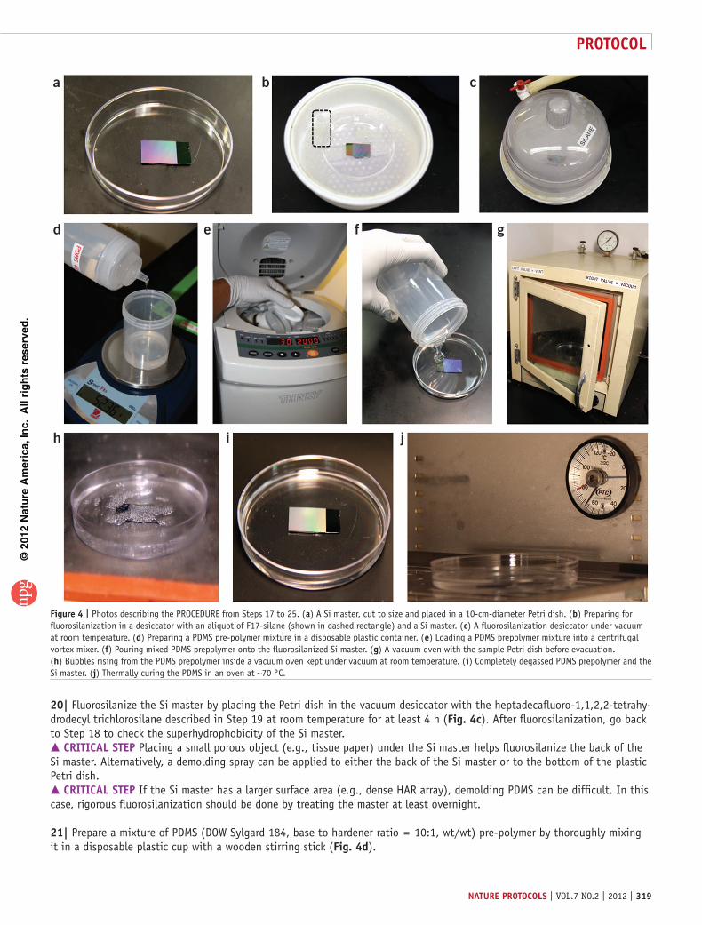
replication of a si master ● tIMInG 4–8 h17| Prepare a Si master from Step 16 by cutting it into a desired size. On a cleanroom paper and with gloved hands, use a diamond-tipped scriber to score a straight line ~5 mm long from the edge perpendicular to the wafer flat (flat edge of a Si wafer). Grab the wafer with gloved hands on both sides of the scored line, as close as possible to the scored line (use tweez-ers if the area is too close to the pattern) and gently bend the wafer to open a gap from the scored line. This will easily snap the wafer into two pieces with straight cuts. Repeat this procedure perpendicular to the cleaved orientation to cut out a rectangular or square piece of Si master of desired size and place it in a plastic Petri dish (Fig. 4a). crItIcal step Choose a Petri dish that is at least twice as large as the Si master. This minimizes the risk of breaking the Si master when demolding the PDMS mold from the Petri dish.
18| Check whether the surface of the Si master is superhydrophobic by placing a droplet of water onto the patterned area and rolling it. If the droplet is pinned and has a small contact angle (typically less than 90°), proceed to the next step for fluor-osilanization. If the surface is superhydrophobic (i.e., the water contact angle is greater than 150°), proceed to Step 21.
19| Prepare an aliquot (200 µl) of heptadecafluoro-1,1,2,2-tetrahydrodecyl trichlorosilane in an open glass vial and place it in a vacuum desiccator without the cap (Fig. 4b).
©20
12 N
atu
re A
mer
ica,
Inc.
All
rig
hts
res
erve
d.
protocol
nature protocols | VOL.7 NO.2 | 2012 | 319
20| Fluorosilanize the Si master by placing the Petri dish in the vacuum desiccator with the heptadecafluoro-1,1,2,2-tetrahy-drodecyl trichlorosilane described in Step 19 at room temperature for at least 4 h (Fig. 4c). After fluorosilanization, go back to Step 18 to check the superhydrophobicity of the Si master. crItIcal step Placing a small porous object (e.g., tissue paper) under the Si master helps fluorosilanize the back of the Si master. Alternatively, a demolding spray can be applied to either the back of the Si master or to the bottom of the plastic Petri dish. crItIcal step If the Si master has a larger surface area (e.g., dense HAR array), demolding PDMS can be difficult. In this case, rigorous fluorosilanization should be done by treating the master at least overnight.
21| Prepare a mixture of PDMS (DOW Sylgard 184, base to hardener ratio = 10:1, wt/wt) pre-polymer by thoroughly mixing it in a disposable plastic cup with a wooden stirring stick (Fig. 4d).
a
d e f g
h i j
b c
SILA
NE
Figure 4 | Photos describing the PROCEDURE from Steps 17 to 25. (a) A Si master, cut to size and placed in a 10-cm-diameter Petri dish. (b) Preparing for fluorosilanization in a desiccator with an aliquot of F17-silane (shown in dashed rectangle) and a Si master. (c) A fluorosilanization desiccator under vacuum at room temperature. (d) Preparing a PDMS pre-polymer mixture in a disposable plastic container. (e) Loading a PDMS prepolymer mixture into a centrifugal vortex mixer. (f) Pouring mixed PDMS prepolymer onto the fluorosilanized Si master. (g) A vacuum oven with the sample Petri dish before evacuation. (h) Bubbles rising from the PDMS prepolymer inside a vacuum oven kept under vacuum at room temperature. (i) Completely degassed PDMS prepolymer and the Si master. (j) Thermally curing the PDMS in an oven at ~70 °C.

©20
12 N
atu
re A
mer
ica,
Inc.
All
rig
hts
res
erve
d.
protocol
320 | VOL.7 NO.2 | 2012 | nature protocols
crItIcal step Use a planetary vortex mixer to facilitate fast mixing without creating trapped air bubbles and to prepare a reproducibly homogeneous mixture (Fig. 4e).
22| Remove trapped air bubbles by placing the PDMS pre-polymer mixture in a vacuum oven at room temperature. crItIcal step Do not heat the oven. PDMS pre-polymer mixture will cure rapidly at elevated temperatures. crItIcal step PDMS pre-polymer mixture has a limited pot life. Degassing time should not exceed 30 min. Leaving the mixture at room temperature for more than 1 h increases the viscosity of the mixture and makes the entire subsequent process extremely difficult. For more information, see the manufacturer’s website: http://www.dowcorning.com/applications/search/products/Details.aspx?prod=01064291&type=PROD.
23| Carefully pour the degassed, bubble-free PDMS pre-polymer mixture over the Si master in the Petri dish from Step 20 (Fig. 4f). crItIcal step Be careful not to generate an excessive amount of extra bubbles and not to damage the Si master while pouring PDMS pre-polymer.
24| Place the Petri dish under vacuum at room temperature to completely remove trapped air bubbles. The degassing time is 5–30 min (Fig. 4g–i). crItIcal step If a few bubbles persist, take the Petri dish out and then carefully move the remaining bubbles away from the Si master pattern with a wooden stick. If the Si master slides from the center or is tilted, carefully reposition it to the center and the bottom of the Petri dish with a wooden stick.
25| Cure the PDMS in an oven (~70 °C) for about 2 h. Ensure that the oven is evenly leveled so that the Si master stays in the center (Fig. 4j). pause poInt PDMS can be left overnight for curing in the oven.? trouBlesHootInG
26| Remove the Petri dish with cured PDMS and the Si master from the oven and let it cool to room temperature.
27| Be extremely gentle when handling the PDMS mold, and carefully start demolding it from the Petri dish by lifting, with a spatula, the mold from an edge (Fig. 5a). Look at the back of the Si master through the bottom of the Petri dish while slowly demolding the entire Si master and PDMS mold. An advancing air gap between the PDMS mold and the Petri dish along the peeling direction should be clearly visible while demolding. We recommend maintaining the speed of the advancing of the air gap below 5 mm s − 1.
28| After removing the PDMS mold, score the PDMS mold along the edges of the Si master (from the flat, back part of it) using a razor blade (Fig. 5b).
29| Place the PDMS mold on a flat surface with the patterned area of the Si master facing up, and then bend the PDMS mold to demold it from the Si master. Use a spatula or a tweezer to hold the Si master onto the bottom surface (Fig. 5c,d). crItIcal step Do not bend the Si master as it can easily break. Never go back once the gap between the PDMS mold and the Si master is made, or the Si master will be damaged.
30| Remove the thin PDMS film on the back of the Si master and place the Si master back into storage.
31| The edges of the PDMS mold usually have a meniscus shape. Cut the extra PDMS surrounding the negative pattern of the Si master to remove these meniscus-shaped areas. This ensures that the back of the PDMS mold is flat (Fig. 5e).
32| Apply UV-curable epoxy (UVO-114) onto the PDMS mold to cover a desired area for replication. Use a plastic disposable pipette to remove bubbles (Fig. 5f). UV-curable epoxy may be degassed under vacuum at room temperature before use.
33| Cover the poured UV-curable epoxy with a precleaned glass slide. Starting from one edge to another helps avoid bubble formation (Fig. 5g). The glass slides may need to be precut to desired sizes.
34| Cure the UV-curable epoxy (~100 mW at 365 nm, for 20–25 min) and let it cool to room temperature (Fig. 5h,i).
©20
12 N
atu
re A
mer
ica,
Inc.
All
rig
hts
res
erve
d.
protocol
nature protocols | VOL.7 NO.2 | 2012 | 321
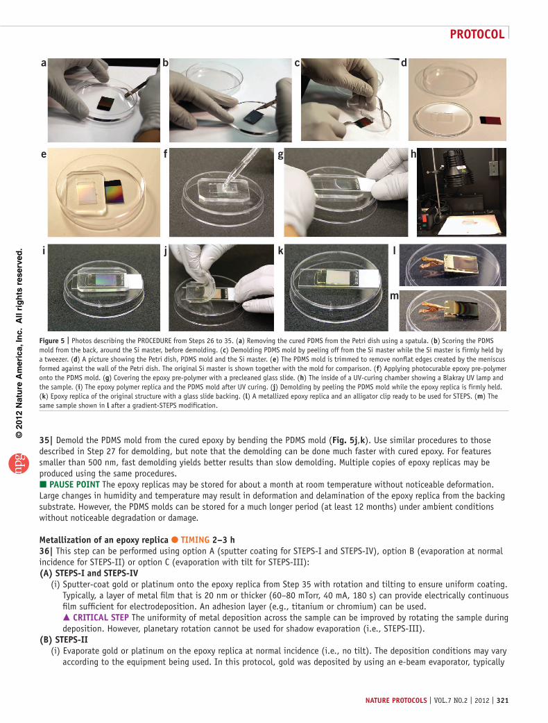
35| Demold the PDMS mold from the cured epoxy by bending the PDMS mold (Fig. 5j,k). Use similar procedures to those described in Step 27 for demolding, but note that the demolding can be done much faster with cured epoxy. For features smaller than 500 nm, fast demolding yields better results than slow demolding. Multiple copies of epoxy replicas may be produced using the same procedures. pause poInt The epoxy replicas may be stored for about a month at room temperature without noticeable deformation. Large changes in humidity and temperature may result in deformation and delamination of the epoxy replica from the backing substrate. However, the PDMS molds can be stored for a much longer period (at least 12 months) under ambient conditions without noticeable degradation or damage.
Metallization of an epoxy replica ● tIMInG 2–3 h36| This step can be performed using option A (sputter coating for STEPS-I and STEPS-IV), option B (evaporation at normal incidence for STEPS-II) or option C (evaporation with tilt for STEPS-III):(a) steps-I and steps-IV (i) Sputter-coat gold or platinum onto the epoxy replica from Step 35 with rotation and tilting to ensure uniform coating.
Typically, a layer of metal film that is 20 nm or thicker (60–80 mTorr, 40 mA, 180 s) can provide electrically continuous film sufficient for electrodeposition. An adhesion layer (e.g., titanium or chromium) can be used. crItIcal step The uniformity of metal deposition across the sample can be improved by rotating the sample during deposition. However, planetary rotation cannot be used for shadow evaporation (i.e., STEPS-III).
(B) steps-II (i) Evaporate gold or platinum on the epoxy replica at normal incidence (i.e., no tilt). The deposition conditions may vary
according to the equipment being used. In this protocol, gold was deposited by using an e-beam evaporator, typically
a
e
i j k l
m
g h
c d
f
b
Figure 5 | Photos describing the PROCEDURE from Steps 26 to 35. (a) Removing the cured PDMS from the Petri dish using a spatula. (b) Scoring the PDMS mold from the back, around the Si master, before demolding. (c) Demolding PDMS mold by peeling off from the Si master while the Si master is firmly held by a tweezer. (d) A picture showing the Petri dish, PDMS mold and the Si master. (e) The PDMS mold is trimmed to remove nonflat edges created by the meniscus formed against the wall of the Petri dish. The original Si master is shown together with the mold for comparison. (f) Applying photocurable epoxy pre-polymer onto the PDMS mold. (g) Covering the epoxy pre-polymer with a precleaned glass slide. (h) The inside of a UV-curing chamber showing a Blakray UV lamp and the sample. (i) The epoxy polymer replica and the PDMS mold after UV curing. (j) Demolding by peeling the PDMS mold while the epoxy replica is firmly held. (k) Epoxy replica of the original structure with a glass slide backing. (l) A metallized epoxy replica and an alligator clip ready to be used for STEPS. (m) The same sample shown in l after a gradient-STEPS modification.
©20
12 N
atu
re A
mer
ica,
Inc.
All
rig
hts
res
erve
d.
protocol
322 | VOL.7 NO.2 | 2012 | nature protocols
at 30–40% power of 9.8 kV (0.2–0.3 A) under a 10 − 6 Torr/5 × 10 − 7 Torr chamber/base pressure, which gave a 1.9–2.0 Å s − 1 deposition rate (Fig. 5l).? trouBlesHootInG
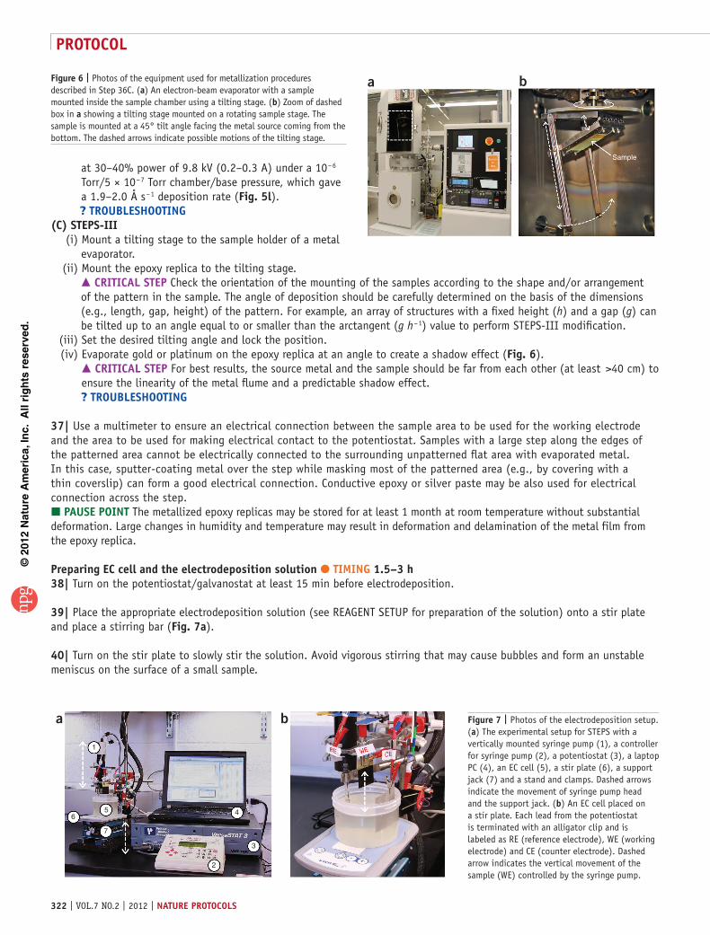
(c) steps-III (i) Mount a tilting stage to the sample holder of a metal
evaporator. (ii) Mount the epoxy replica to the tilting stage.
crItIcal step Check the orientation of the mounting of the samples according to the shape and/or arrangement of the pattern in the sample. The angle of deposition should be carefully determined on the basis of the dimensions (e.g., length, gap, height) of the pattern. For example, an array of structures with a fixed height (h) and a gap (g) can be tilted up to an angle equal to or smaller than the arctangent (g h − 1) value to perform STEPS-III modification.
(iii) Set the desired tilting angle and lock the position. (iv) Evaporate gold or platinum on the epoxy replica at an angle to create a shadow effect (Fig. 6).
crItIcal step For best results, the source metal and the sample should be far from each other (at least >40 cm) to ensure the linearity of the metal flume and a predictable shadow effect.? trouBlesHootInG
37| Use a multimeter to ensure an electrical connection between the sample area to be used for the working electrode and the area to be used for making electrical contact to the potentiostat. Samples with a large step along the edges of the patterned area cannot be electrically connected to the surrounding unpatterned flat area with evaporated metal. In this case, sputter-coating metal over the step while masking most of the patterned area (e.g., by covering with a thin coverslip) can form a good electrical connection. Conductive epoxy or silver paste may be also used for electrical connection across the step. pause poInt The metallized epoxy replicas may be stored for at least 1 month at room temperature without substantial deformation. Large changes in humidity and temperature may result in deformation and delamination of the metal film from the epoxy replica.
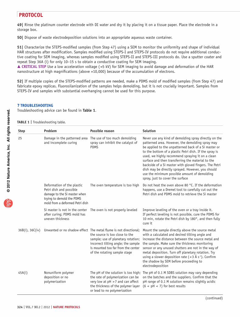
preparing ec cell and the electrodeposition solution ● tIMInG 1.5–3 h38| Turn on the potentiostat/galvanostat at least 15 min before electrodeposition.
39| Place the appropriate electrodeposition solution (see REAGENT SETUP for preparation of the solution) onto a stir plate and place a stirring bar (Fig. 7a).
40| Turn on the stir plate to slowly stir the solution. Avoid vigorous stirring that may cause bubbles and form an unstable meniscus on the surface of a small sample.
a b
Sample
Figure 6 | Photos of the equipment used for metallization procedures described in Step 36C. (a) An electron-beam evaporator with a sample mounted inside the sample chamber using a tilting stage. (b) Zoom of dashed box in a showing a tilting stage mounted on a rotating sample stage. The sample is mounted at a 45° tilt angle facing the metal source coming from the bottom. The dashed arrows indicate possible motions of the tilting stage.
a b
1
65
7
2
4
3
Figure 7 | Photos of the electrodeposition setup. (a) The experimental setup for STEPS with a vertically mounted syringe pump (1), a controller for syringe pump (2), a potentiostat (3), a laptop PC (4), an EC cell (5), a stir plate (6), a support jack (7) and a stand and clamps. Dashed arrows indicate the movement of syringe pump head and the support jack. (b) An EC cell placed on a stir plate. Each lead from the potentiostat is terminated with an alligator clip and is labeled as RE (reference electrode), WE (working electrode) and CE (counter electrode). Dashed arrow indicates the vertical movement of the sample (WE) controlled by the syringe pump.

©20
12 N
atu
re A
mer
ica,
Inc.
All
rig
hts
res
erve
d.
protocol
nature protocols | VOL.7 NO.2 | 2012 | 323
41| Position the reference electrode, the counter electrode and the working electrode (sample), and then lift the sup-port jack to immerse the electrodes in the electrodeposition solution. Use the syringe pump to move the working electrode vertically. For best results, place the front surface of the sample (working electrode) parallel to and facing the center of the counter electrode. Ensure that the working electrode and the counter electrode are not in direct contact with each other. The reference electrode can be placed almost anywhere in the solution. However, avoid placing it in between the working and the counter electrode (Fig. 7b).
42| Connect the electrodes to the leads from the potentiostat/galvanostat.
electrodeposition of ppy ● tIMInG 0.5–1 h per sample43| Set the experimental parameters (reference electrode type, surface area, type of experiment, potential, time and so on) for electrodeposition in the software running the potentiostat/galvanostat. Typical parameters are as follows: reference electrode = Ag/AgCl (saturated with NaCl), electrode type: solid, area of working electrode = 1 cm2, type of experiment = chronoamperometry. See Step 45 for potential and time.
44| Set the syringe pump settings for desired speed of sample movement if gradient-STEPS is used. crItIcal step For gradient-STEPS, use the syringe pump to withdraw the sample from the electrodeposition solution while the electrodeposition is in process. Multiple gradient-STEPS may be performed on a single substrate.
45| Run the electrodeposition to electropolymerize PPy. This step can be performed using option A (for STEPS-I, STEPS-II and STEPS-III) or option B (for STEPS-IV).(a) steps-I, steps-II and steps-III (i) Use chronoamperometry (constant potential) at 0.55–0.65 V versus Ag/AgCl in 0.1 M pyrrole/0.1 M SDBS solution. The
typical deposition rate is 35–45 nm min − 1 at 0.55 V. This solution can be used for about five depositions. STEPS-II and STEPS-III only work for original structures prepared using the Bosch etching method, in which there is a considerable sidewall corrugation (‘scallop’).? trouBlesHootInG
(B) steps-IV (i) Use chronoamperometry (constant potential) at 0.85 V versus Ag/AgCl in 0.08 M pyrrole/0.07 M LiClO4/0.25 M PBS
(pH = 5.5) solution. The typical deposition time is 300–600 s. This solution can be used for about five depositions.? trouBlesHootInG
46| Stop the syringe pump if gradient-STEPS was used. An example of a sample modified by gradient-STEPS is shown in (Fig. 5m).
47| Rinse and dry the sample. This step can be performed using option A for nonclustering samples (final modified structures typically have a low aspect ratio or a large distance between neighboring structures, i.e., large pitch) or option B for clustering samples (final modified structures typically have a HAR or a small distance between neighboring structures, i.e., small pitch).(a) nonclustering sample (i) Rinse the sample with DI water. (ii) Dry the sample slowly by evaporation or under a stream of dry air or nitrogen.(B) clustering sample (i) Rinse the sample with DI water but never let it dry by itself. (ii) Gradually exchange the solution from DI water to absolute ethanol by immersing it in ethanol and repeatedly
decanting the excess ethanol and refilling with fresh ethanol. (iii) Use a critical point dryer to dry the sample. Note that additional time (1–2 h) would be needed for this step. ? trouBlesHootInG
cleaning and wrap-up ● tIMInG 0.5–1 h48| Rinse the reference electrode with DI water and dry it immediately by blowing it with dry air or nitrogen, and then store it in a saturated NaCl solution. For a long-term storage, wrap the Vycor seal with paraffin film to keep the electrode-filling solution from drying over time.
©20
12 N
atu
re A
mer
ica,
Inc.
All
rig
hts
res
erve
d.
protocol
324 | VOL.7 NO.2 | 2012 | nature protocols
taBle 1 | Troubleshooting table.
step problem possible reason solution
25 Damage in the patterned area and incomplete curing
The use of too much demolding spray can inhibit the catalyst of PDMS
Never use any kind of demolding spray directly on the patterned area. However, the demolding spray may be applied to the unpatterned back of a Si master or to the bottom of a plastic Petri dish. If the spray is used, we highly recommend spraying it on a clean surface and then transferring the material to the backside of a Si master with gloved fingers. The Petri dish may be directly sprayed. However, you should use the minimum possible amount of demolding spray, just to cover the surface
Deformation of the plastic Petri dish and possible damage to the Si master when trying to demold the PDMS mold from a deformed Petri dish
The oven temperature is too high Do not heat the oven above 80 °C. If the deformation happens, use a Dremel tool to carefully cut out the Petri dish and PDMS mold to retrieve the Si master
Si master is not in the center after curing; PDMS mold has uneven thickness
The oven is not properly leveled Improve leveling of the oven or a tray inside it. If perfect leveling is not possible, cure the PDMS for 10 min, rotate the Petri dish by 180°, and then fully cure it
36B(i), 36C(iv) Unwanted or no shadow effect The metal flume is not directional; the source is too close to the sample; use of planetary rotation; incorrect tilting angle; the sample is mounted too far from the center of the rotating sample stage
Mount the sample directly above the source metal with a calculated and desired tilting angle and increase the distance between the source metal and the sample. Make sure the thickness monitoring sensor or any unused shutters are not in the way of metal deposition. Turn off planetary rotation. Try using a slower deposition rate ( < 3 Å s-1). Confirm the shadow by SEM before proceeding to electrodeposition
45A(i) Nonuniform polymer deposition or no polymerization
The pH of the solution is too high; the rate of polymerization can be very low at pH > 7 and can affect the thickness of the polymer layer or lead to no polymerization
The pH of 0.1 M SDBS solution may vary depending on the batches and the suppliers. Confirm that the pH range of 0.1 M solution remains slightly acidic (6 < pH < 7) for best results
49| Rinse the platinum counter electrode with DI water and dry it by placing it on a tissue paper. Place the electrode in a storage box.
50| Dispose of waste electrodeposition solutions into an appropriate aqueous waste container.
51| Characterize the STEPS-modified samples (from Step 47) using a SEM to monitor the uniformity and shape of individual HAR structures after modification. Samples modified using STEPS-I and STEPS-IV protocols do not require additional conduc-tive coating for SEM imaging, whereas samples modified using STEPS-II and STEPS-III protocols do. Use a sputter coater and repeat Step 36A (i) for only 10–15 s to obtain a conductive coating for SEM imaging. crItIcal step Use a low acceleration voltage ( <5 kV) for SEM imaging to avoid damage and deformation of the HAR nanostructure at high magnifications (above ×10,000) because of the accumulation of electrons.
52| If multiple copies of the STEPS-modified patterns are needed, make a PDMS mold of modified samples (from Step 47) and fabricate epoxy replicas. Fluorosilanization of the samples helps demolding, but it is not crucially important. Samples from STEPS-IV and samples with substantial overhanging cannot be used for this purpose.
? trouBlesHootInGTroubleshooting advice can be found in table 1.
(continued)
©20
12 N
atu
re A
mer
ica,
Inc.
All
rig
hts
res
erve
d.
protocol
nature protocols | VOL.7 NO.2 | 2012 | 325
● tIMInGSteps 1 and 2, mask design and fabrication: 1–2 weeksSteps 3–16, Si master fabrication: 6–10 hSteps 17–35, replication of a Si master: 4–8 hSteps 36 and 37, metallization of an epoxy replica: 2–3 hSteps 38–42, preparation of EC cell and reagents for electrochemical deposition: 1.5–3 hSteps 43–47, electrodeposition of PPy: 0.5–1 h per sample (extra 1–2 h if critical point drying samples)Steps 48–52, cleaning and wrap-up: 0.5–1 h
antIcIpateD resultsWith this protocol, one should be able to replicate a Si master into polymeric substrates through PDMS molding. This proto-col also provides step-by-step procedures for fabricating a Si master to make the protocol self-contained.
Starting from replicated polymeric HAR structures, one should be able to create uniformly and proportion-ally modified HAR structures and gradient substrates using each STEPS method. In STEPS-II and STEPS-III, one should first expect proper met-allization as shown in the example SEM images of e-beam-evaporated metal-coated epoxy posts in Figure 8. A typical example current versus time curve from chronoam-perometry (constant potential mode) experiments used in STEPS-I, STEPS-II, STEPS-III and a gradient version of them are given in Figure 9. The color of the substrate gradually changes to light blue, dark blue and then to black on increasing the
2 µm
a
d e f
b c
1 µm 5 µm 1 µm
1 µm 1 µm
Figure 8 | SEM images of microposts metallized for STEPS-II and STEPS-III. (a) Micropost array covered with electron-beam–evaporated 50-nm-thick gold at normal incidence for STEPS-II process. (b) Top view of a metallized micropost before STEPS-II process. (c) Top view of the micropost shown in b after STEPS-II modification. (d) A micropost array covered with electron beam–evaporated 50-nm-thick gold at a 45° tilt angle for STEPS-III process (a low-magnification image is shown inset). (e) Microposts in d broken down to show the discontinuity of the gold electrodes on scallops. (f) Microposts in e after oxygen plasma treatment to remove the epoxy posts. Typical ‘spine and ribs’ structures of the deposited metal remain.
taBle 1 | Troubleshooting table (continued).
step problem possible reason solution
45A(i), 45B(i) Nonuniformity, or poor surface coverage of electrodeposited polymer
The surface area of counter elec-trode (CE) is too small compared with that of the working electrode (WE) and is limiting the Faradaic current; the amount of available pyrrole in solution has markedly decreased; the WE and CE are too far from each other; stirring is excessive; the temperature in the bath is nonuniform; the elec-trodeposition solution is evaporat-ing too quickly
Use a CE with large surface area or reduce the size of the WE (surface area ratio of 10:1 (CE/WE) or greater is recommended). Replace the solution after approxi-mately six electrodepositions. Place the patterned area facing parallel to the CE. Give enough time to cool the electrodeposition solution to room tem-perature, which may have been heated by ultrasonic processing. Use mild stirring
47B(iii) Clustering of nanostructures after drying samples
For samples having patterns of arrays of closely spaced HAR nanostructures, evaporation of liquid after rinsing may cause them to cluster because of a large capillary force competing with elasticity of the structure, adhesion between the structures and associated kinetics5,10
Let the sample dry slowly for microscale structures. If the problem persists, use critical point drying
©20
12 N
atu
re A
mer
ica,
Inc.
All
rig
hts
res
erve
d.
protocol
326 | VOL.7 NO.2 | 2012 | nature protocols
deposition time (or thickness). A typical example current versus time curve from a STEPS-IV modification is shown in Figure 10. The color of the substrate gradually changes to light blue, dark blue and then to black on increasing the deposition time (or thickness). Typical example SEM images of modified structures using each STEPS method are provided in Figure 2.
Most of the STEPS-modified patterns can be used as new masters in the PDMS molding process unless they have signifi-cant overhanging features or are produced by STEPS-IV. By using sequential STEPS modification and replication, one should be able to produce even more complex HAR structures or gradient substrates with multiply graded feature sizes and shapes (e.g., the gradient of the cone structure along x axis and the gradient of the diameter along the y axis).
2.5 ma
c
Cur
rent
(A
)C
urre
nt (
A) 2.0 m
1.5 m
1.5 m
1.4 m
1.3 m
1.2 m
1.1 m
1.0 m
1.0 m
500.0 µ
00
100 200 300
Elapsed time (s)
400 500 600
0 100 200 300Elapsed time (s)
400 500 600
d
b1.4 m
1.3 m
1.3 m
1.2 m
Cur
rent
(A
)C
urre
nt (
A)
1.2 m
1.1 m
1.1 m
5.5 m
5.0 m
4.5 m
4.0 m
3.5 m
–20
–20
0
0
20 40 60 80 100 120
20 40 60 80 100 120 140 160
Elapsed time (s)
Elapsed time (s)
Figure 9 | Typical current versus time graphs obtained from a chronoamperometry experiment used for STEPS-I, STEPS-II and STEPS-III. (a–d) Shown are graphs from experiments on a flat substrate (a), on a patterned substrate (b), in gradient–STEPS with the immersion of patterned substrate (c), and in gradient–STEPS with the withdrawal of patterned substrate (d).
3.5 m
3.0 m
2.5 m
2.0 m
1.5 m
Cur
rent
(A
)
1.0 m
500.0 µ
0
0 100 200 300 400
Elapsed time (s)
500 600
Figure 10 | Typical current versus time graph obtained from a STEPS-IV experiment. The current gradually increases as the nanofibers grow.
Note: Supplementary information is available via the HTML version of this article.
acknoWleDGMents This work was partially supported by the US Department of Energy, Office of Basic Energy Sciences and the Division of Materials Science and Engineering, under award no. DE-SC0005247 (design of HAR structures); the US Army Research Office Multidisciplinary University Research Initiative under award no. W911NF-09-1-0476 (electrodeposition and mechanical properties); and the US Air Force Office of Scientific Research Multidisciplinary University Research Initiative under award no. FA9550-09-1-0669-DOD35CAP (optical properties). This work was carried out in part through the use of the Massachusetts Institute of Technology’s Microsystems Technology Laboratories. Part of this work was also performed at the Center for Nanoscale Systems at Harvard University, a member of the National Nanotechnology Infrastructure Network, which is supported by the National Science Foundation (NSF) under NSF award no. ECS-0335765. W.E.A.-M. thanks REU BRIDGE, co-funded by the ASSURE program of the Department of Defense in partnership with the National Science Foundation REU Site program under NSF grant no. DMR-1005022. We thank J.C. Weaver for help in manuscript preparation and E. Macomber for technical assistance with metal deposition equipment.
autHor contrIButIons P.K. and J.A. co-invented the STEPS method. J.A. supervised the project and advised on the applications of STEPS. M.K. and P.K. designed the masks. M.K. fabricated the reticles and the Si masters. P.K. and W.E.A.-M. performed replication, metallization and electrochemical deposition experiments and the characterization and analysis of the STEPS-modified structures. P.K., W.E.A.-M., M.K. and J.A. wrote the manuscript.
coMpetInG FInancIal Interests The authors declare no competing financial interests.
Published online at http://www.natureprotocols.com/. Reprints and permissions information is available online at http://www.nature.com/reprints/index.html.
1. Kim, P. et al. Structural transformation by electrodeposition on patterned substrates (STEPS): a new versatile nanofabrication method. Nano. Lett. published online, doi:10.1021/nl200426g (25 March 2011).
2. Ahuja, A. et al. Nanonails: a simple geometrical approach to electrically tunable superlyophobic surfaces. Langmuir 24, 9–14 (2008).
3. Chu, K.-H., Xiao, R. & Wang, E.N. Uni-directional liquid spreading on asymmetric nanostructured surfaces. Nat. Mater. 9, 413–417 (2010).
4. Hochbaum, A.I. & Aizenberg, J. Bacteria pattern spontaneously on periodic nanostructure arrays. Nano. Lett. 10, 3717–3721 (2010).
5. Kang, S.H., Pokroy, B., Mahadevan, L. & Aizenberg, J. Control of shape and size of nanopillar assembly by adhesion-mediated elastocapillary interaction. ACS Nano. 4, 6323–6331 (2010).
6. Kim, P., Zarzar, L.D., He, X., Grinthal, A. & Aizenberg, J. Hydrogel-actuated integrated responsive systems (HAIRS): moving towards adaptive materials. Curr. Opin. Solid State Mater. Sci. 15, 236–245 (2011).
7. Kim, P., Zarzar, L.D., Zhao, X., Sidorenko, A. & Aizenberg, J. Microbristle in gels: toward all-polymer reconfigurable hybrid surfaces. Soft Matter 6, 750–755 (2010).
8. Mishchenko, L. et al. Design of ice-free nanostructured surfaces based on repulsion of impacting water droplets. ACS Nano. 4, 7699–7707 (2010).
9. Pokroy, B., Epstein, A.K., Persson-Gulda, M.C.M. & Aizenberg, J. Fabrication of bioinspired actuated nanostructures with arbitrary geometry and stiffness. Adv. Mater. 21, 463–469 (2009).

©20
12 N
atu
re A
mer
ica,
Inc.
All
rig
hts
res
erve
d.
protocol
nature protocols | VOL.7 NO.2 | 2012 | 327
10. Pokroy, B., Kang, S.H., Mahadevan, L. & Aizenberg, J. Self-organization of a mesoscale bristle into ordered, hierarchical helical assemblies. Science 323, 237–238 (2009).
11. Schumacher, J.F. et al. Engineered antifouling microtopographies—effect of feature size, geometry, and roughness on settlement of zoospores of the green alga Ulva. Biofouling 23, 55–62 (2007).
12. Sidorenko, A., Krupenkin, T., Taylor, A., Fratz, P. & Aizenberg, J. Reversible switching of hydrogel-actuated nanostructures into complex micropatterns. Science 315, 487–490 (2007).
13. Tuteja, A. et al. Designing superoleophobic surfaces. Science 318, 1618–1622 (2007).
14. Vasquez, Y., Fenton, E.M., Chernow, V.F. & Aizenberg, J. Growth of polygonal rings and wires of CuS on structured surfaces. Crystal Eng. Commun. 13, 1077–1080 (2011).
15. Zarzar, L.D., Kim, P. & Aizenberg, J. Bio-inspired design of submerged hydrogel-actuated polymer microstructures operating in response to pH. Adv. Mater. 23, 1442–1446 (2011).
16. Laermer, F. & Schilp, A. Robert Bosch GmbH Method of anisotropically etching silicon. US patent US5501893 (1996).
17. Lipomi, D.J. et al. Fabrication and replication of arrays of single- or multi-component nanostructures by replica molding and mechanical sectioning. ACS Nano. 4, 4017–4026 (2010).
18. Tran, H.D., Li, D. & Kaner, R.B. One-dimensional conducting polymer nanostructures: bulk synthesis and applications. Adv. Mater. 21, 1487–1499 (2009).
19. Zang, J. et al. Template-free electrochemical synthesis of superhydrophilic polypyrrole nanofiber network. Macromolecules 41, 7053–7057 (2008).
20. Debiemme-Chouvy, C. Template-free one-step electrochemical formation of polypyrrole nanowire array. Electrochem. Commun. 11, 298–301 (2009).
21. Zhang, Y., Lin, C.-T. & Yang, S. Fabrication of hierarchical pillar arrays from thermoplastic and photosensitive SU-8. Small 6, 768–775 (2010).
22. Zhang, Y., Reed, J.C. & Yang, S. Creating a library of complex metallic nanostructures via harnessing pattern transformation of a single PDMS membrane. ACS Nano. 3, 2412–2418 (2009).
23. Lee, M.H., Huntington, M.D., Zhou, W., Yang, J.-C. & Odom, T.W. Programmable soft lithography: solvent-assisted nanoscale embossing. Nano. Lett. 11, 311–315 (2011).
24. Bhushan, B. & Jung, Y.C. Natural and biomimetic artificial surfaces for superhydrophobicity, self-cleaning, low adhesion, and drag reduction. Prog. Mater. Sci. 56, 1–108 (2011).
25. Kamperman, M., Arzt, E. & del Campo, A. Bioinspired Patterned Adhesives 1st edn (Wiley-VCH Verlag GmbH & Co. KgaA,, 2011).
26. Jeong, H.E. & Suh, K.Y. Nanohairs and nanotubes: efficient structural elements for gecko-inspired artificial dry adhesives. Nano. Today 4, 335–346 (2009).
27. Xu, Q., Rioux, R.M., Dickey, M.D. & Whitesides, G.M. Nanoskiving: a new method to produce arrays of nanostructures. Acc. Chem. Res. 41, 1566–1577 (2008).
28. Yang, M.T., Fu, J., Wang, Y.-K., Desai, R.A. & Chen, C.S. Assaying stem cell mechanobiology on microfabricated elastomeric substrates with geometrically modulated rigidity. Nat. Protoc. 6, 187–212 (2011).
29. Discher, D.E., Janmey, P. & Wang, Y.-l. Tissue cells feel and respond to the stiffness of their substrate. Science 310, 1139–1143 (2005).
30. Bettinger, C.J., Langer, R. & Borenstein, J.T. Engineering substrate topography at the micro- and nanoscale to control cell function. Angew. Chem. Int. Ed. 48, 5406–5415 (2009).
31. Chen, C.S., Mrksich, M., Huang, S., Whitesides, G.M. & Ingber, D.E. Geometric control of cell life and death. Science 276, 1425–1428 (1997).
32. Davey, M.E. & O’toole, G.A. Microbial biofilms: from ecology to molecular genetics. Microbiol. Mol. Biol. Rev. 64, 847–867 (2000).
33. Volder, M.D. et al. Diverse 3D microarchitectures made by capillary forming of carbon nanotubes. Adv. Mater. 22, 4384–4389 (2010).
34. Chandra, D. & Yang, S. Capillary-force-induced clustering of micropillar arrays: is it caused by isolated capillary bridges or by the lateral capillary meniscus interaction force? Langmuir 25, 10430–10434 (2009).
35. Das, M., Wilson, K., Molnar, P. & Hickman, J.J. Differentiation of skeletal muscle and integration of myotubes with silicon microstructures using serum-free medium and synthetic silane substrate. Nat. Protoc. 2, 1795–1801 (2007).
36. Fu, J., Mao, P. & Han, J. Continuous-flow bioseparation using microfabricated anisotropic nanofluidic sieving structures. Nat. Protoc. 4, 1681–1698 (2009).
37. Fu, J. et al. Mechanical regulation of cell function with geometrically modulated elastomeric substrates. Nat. Methods 7, 733–736 (2010).
38. Qin, D., Xia, Y. & Whitesides, G.M. Soft lithography for micro- and nanoscale patterning. Nat. Protoc. 5, 491–502 (2010).
39. Maluf, N. An Introduction to Microelectromechanical System Engineering (Artech House, 2000).
40. Ayón, A.A., Braff, R., Bayt, R., Sawin, H.H. & Schmidt, M.A. Influence of coil power on the etching characteristics in a high density plasma etcher. J. Electrochem. Soc. 146, 2730–2736 (1999).
41. Ayón, A.A., Braff, R., Lin, C.C., Sawin, H.H. & Schmidt, M.A. Characterization of a time multiplexed inductively coupled plasma etcher. J. Electrochem. Soc. 146, 339–349 (1999).


![TOPOLOGICALLY SLICE KNOTS WITH NONTRIVIAL ...arXiv:1001.1538v3 [math.GT] 7 May 2011 TOPOLOGICALLY SLICE KNOTS WITH NONTRIVIAL ALEXANDER POLYNOMIAL MATTHEW HEDDEN, CHARLES LIVINGSTON,](https://img.pdfslide.net/doc/110x75/5f8d8100ff950450d4784567/topologically-slice-knots-with-nontrivial-arxiv10011538v3-mathgt-7-may.jpg)