Embed Size (px)
Citation preview
EPJ Photovoltaics 3, 30303 (2012)www.epj-pv.orgDOI: 10.1051/epjpv/2012010c© Owned by the authors, published by EDP Sciences, 2012
EPJ PhotovoltaicsEPJ Photovoltaics
Epitaxial growth of silicon and germanium on (100)-orientedcrystalline substrates by RF PECVD at 175 ◦C
M. Labrune1,2,a, X. Bril1, G. Patriarche3, L. Largeau3, O. Mauguin3, and P. Roca i Cabarrocas1
1 LPICM, CNRS-Ecole Polytechnique, 91128 Palaiseau Cedex, France2 TOTAL S.A., Gas & Power, R&D Division, Courbevoie, France3 Laboratoire de Photonique et de Nanostructures, CNRS, Marcoussis, France
Received: 25 January 2012 / Accepted: 14 June 2012Published online: 13 November 2012
Abstract We report on the epitaxial growth of crystalline Si and Ge thin films by standard radio fre-quency plasma enhanced chemical vapor deposition at 175 ◦C on (100)-oriented silicon substrates. We alsodemonstrate the epitaxial growth of silicon films on epitaxially grown germanium layers so that multilayersamples sustaining epitaxy could be produced. We used spectroscopic ellipsometry, Raman spectroscopy,transmission electron microscopy and X-ray diffraction to characterize the structure of the films (amor-phous, crystalline). These techniques were found to provide consistent results and provided informationon the crystallinity and constraints in such lattice-mismatched structures. These results open the way tomultiple quantum-well structures, which have been so far limited to few techniques such as MolecularBeam Epitaxy or MetalOrganic Chemical Vapor Deposition.
1 Introduction
In the field of solar energy, there is a continuous searchfor ways to increase the cost-effectiveness of solar cells.This is particularly the case of crystalline silicon solar cellswhich is the leading technology and covers more than 80%of the PV market. For this technology to keep its advan-tage, reducing the thickness of expensive c-Si wafers ismandatory. Various approaches have already been used toproduce efficient and thin c-Si solar cells resulting in effi-ciencies above 22% for heterojunction c-Si solar cells on awafer thinned down to 98 μm [1]. However this approachstill requires to grow ingots and to slice them into wafers.Another way to cut costs is to grow the mono or multicrystalline silicon directly on a foreign substrate, usingfor instance Chemical Vapor Deposition [2], or on a poly-crystalline seed layer obtained by the crystallization of anamorphous silicon layer, using a catalyst in the case ofaluminium induced crystallization [3] or in a catalyst-freeapproach using solid phase crystallization [4]. However,these processes usually lead to relatively low solar cell ef-ficiencies since there is a non-monotonic relationship be-tween grain size and solar cell efficiency that implies thatin the case of multicrystalline silicon one should have verylarge grains, as reported by Bergmann [5].
More recently the epitaxial growth of Si films onc-Si substrates has been achieved by various techniquessuch as Plasma Enhanced Chemical Vapor Deposition(PECVD) [6], Atmospheric Pressure CVD [7], Inductively
a e-mail: [email protected]
Coupled PECVD [8] as well as by Hot Wire CVD [9]. Inmost of these cases, except in reference [6], the substratewas kept at a relatively high temperature to favor the epi-taxial growth (T � 700 ◦C). These high temperature ap-proaches have resulted in solar cell efficiencies of 17% fora 50 μm thick free-standing c-Si base material epitaxiallygrown on a porous Si substrate before being detached [10],or over 15% by growing a 20 μm thick epitaxial Si baseon a seed substrate and also using diffusion processes [11],and about 7% when growing a 2 μm thick epitaxial layerby HWCVD at 700 ◦C [12].
Alike, epitaxial growth of Ge films was obtained byPECVD on (100) NaCl substrates kept at 450 ◦C dur-ing growth [13] or by Molecular Beam Epitaxy on (100)GaAs [14]. This is of great interest since simulationsdemonstrated the feasibility of efficient structures com-bining Si and Ge materials [15].
Previous results obtained in our laboratory have shownthat it is possible to obtain epitaxial layers of Ge on (100)gallium arsenide (GaAs) substrates [16] and of Si on (100)silicon substrates [17–19], both by RF PECVD and atsubstrate temperature as low as 175 ◦C. By doing so, wehave been able to obtain solar cells with an efficiency ashigh as 7% for an intrinsic absorber layer of 2.4 μm grownat 165 ◦C [19].
2 Experiments
All the samples of this study were deposited in a multi-plasma monochamber reactor PECVD reactor operated at
This is an Open Access article distributed under the terms of the Creative Commons Attribution-Noncommercial License 3.0, which permitsunrestricted use, distribution, and reproduction in any noncommercial medium, provided the original work is properly cited.
EPJ Photovoltaics
Table 1. Process conditions used to grow the epitaxial films of Si and Ge at 175 ◦C.
Film on Film on Pressure SiH4 GeH4 in H2 H2 RF power Deposition rate(111) c-Si (100) c-Si (Torr) (sccm) (sccm) (sccm) (mW/cm2) (A s−1)µc-Ge:H Epitaxial 1.4 0 5 200 31 0.15pm-Si:H Epitaxial 1.2 12 0 200 25 0.5
a frequency of 13.56 MHz [20]. We used (100) and (111)-oriented Si substrates and (100)-oriented GaAs substratesfor the TEM experiments. All the crystalline substrateswere submitted to a 30 s dip in hydrofluoric acid, to re-move the native oxide, prior to being loaded in the re-actor, which was pumped down to a base pressure below7 × 10−7 Torr. We emphasize that this procedure allowsus to achieve heterojonction solar cells with efficienciesup to 17% [18] and even homojonction solar cells whenthe deposited layer is epitaxial [17]. This is a good indi-cation of the excellent surface passivation and of the highquality of the epitaxial doped layers respectively, whenwe use this cleaning procedure and this PECVD reactor.The depositions were performed using silane (SiH4) andhydrogen (H2) gas mixtures for the silicon films and H2
and germane (GeH4, 2%-diluted in H2) gas mixtures forthe germanium films. All the samples were characterizedvia spectroscopic ellipsometry using a phase modulatedellipsometer (UVISEL from HORIBA Jobin-Yvon). TheRaman spectrometer used in this work is a DILOR JobinYvon XY with a He-Ne laser excitation at 632.8 nm. TheTEM microscope is a JEOL 2200 FS, being able to operatein the STEM (scanning TEM) or TEM mode. High an-gle X-ray diffraction and grazing incidence X-ray diffrac-tion measurements have been performed using a RigakuSmartlab high resolution diffractometer equipped with a9 kW rotating anode and a 7-axes goniometer.
3 Results
Previous studies in our laboratory have shown thatplasma conditions leading to hydrogenated microcrys-talline germanium films on glass can eventually lead toan epitaxial growth when applied on a (100)-orientedGaAs substrate [16]. We obtained the same results forsilicon films, for which conditions known to lead to hydro-genated polymorphous silicon (pm-Si:H) on glass lead toepitaxial growth when applied to (100)-oriented Si sub-strates [17, 18, 21]. Other research groups also found thata rather broad range of experimental parameters wouldeventually lead to unwanted epitaxial films on (100) Sisubstrates [22,23]. In the case of heterojunction solar cells,this epitaxy is unwanted since this crystalline layer doesnot provide any surface passivation [22]. However, one cantake benefit of this capability of PECVD to grow thick epi-taxial layers and use them as the active material in solarcells [19] or as the emitter of c-Si solar cells [17].
Table 1 summarizes the plasma conditions used toachieve epitaxy on (100)-oriented substrates for the Si andGe films respectively. Figure 1 shows the SE spectra of amultilayer stack co-deposited on (100) GaAs, (100) Si and
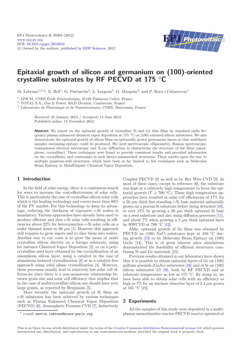
Fig. 1. Imaginary part of the pseudo-dielectric function of themulti layer stack (905071) co-deposited onto various substratesas deduced from SE measurements, the black line correspondsto the fit obtained by modeling the stack deposited on the (100)Si substrate using the optical model described in the inset.
(111) Si. The high photon energy part (3−5 eV) of theSE spectrum is more sensitive to the top and also bulkpart of the films. The last deposited layer being silicon,in Figure 1, we can see the characteristic spectrum of c-Si, which has two peaks around 3.4 and 4.2 eV on bothGaAs and Si (100)-oriented substrates, whereas on (111)c-Si substrate, the silicon films are amorphous (a similarspectrum was measured for the film co-deposited on glass,not shown for clarity). The lower photon energy part ofthe spectrum is sensitive to the bulk and thickness of thefilm, the interference fringes providing information on thethickness of the whole stack. The Bruggeman EffectiveMedium Approximation (BEMA) model [24] used for thefilm grown on (100) Si is shown in the inset of Figure 1and the spectrum obtained from the model is also plot-ted with a dark line. Interestingly, the measurement per-formed on the film grown on the (100) GaAs substrate,can be fitted using the same model as the one used to fitthe measurement performed on the (100) Si. This meansthat we obtained the same stack on both (100) substrates.Even though a fit based on crystalline silicon and ger-manium materials provided a reasonable match with theexperimental data (with a figure of merit χ2 of 2.3), wecould improve the fit (χ2 = 1.5) by using the dielectricfunction of large grains polysilicon material reference fileobtained by Jellison et al. [25] for the silicon layers anda mixture of crystalline germanium and a small fractionof germanium oxide (1−5%), as obtained by Aspnes andStudna [26] for the germanium layers. There are at least
30303-p2
M. Labrune et al.: PECVD epitaxial growth of Si and Ge on (100)-Si substrates at 175 ◦C
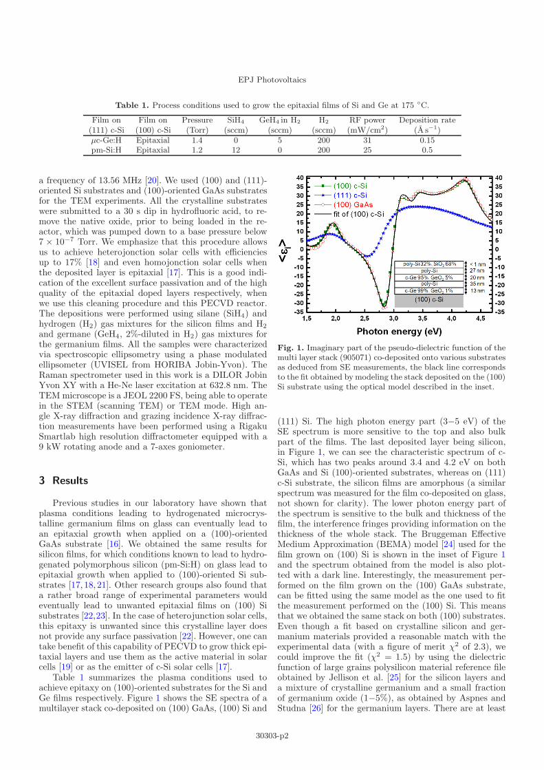
Fig. 2. Raman scattering intensity as a function of the Ramanshift for the multi layer samples (905071) co-deposited on var-ious substrates ((100) GaAs, (100) Si and (111) Si).
two reasons that may explain the better fit when consid-ering polycrystalline dielectric function and introducingGeO2 in the Ge layers. The first one is that we cannotexpect to have films with no roughness so that among ourfour interfaces, none is perfectly flat (as shown by the pres-ence of a surface roughness of about 1 nm in the model ofFig. 1). Introducing a rough interface between each layercould even further reduce χ2 but this is at the cost of dras-tically increasing the number of parameters of the model.The second one is that these films are produced at 175 ◦Cin a standard RF PECVD reactor without load-lock norspecial precaution concerning gas purity (no gas purifiers)so that we can expect our films to contain carbon andoxygen impurities as well as a significant amount of hy-drogen. Those may slightly alter the dielectric functions ofthe materials as compared to their calibrated crystallinecounterparts.
We also investigated the structure of the films byRaman spectroscopy. The Raman spectra of the stack de-posited on the three substrates are shown in Figure 2, thesubstrates being (100) GaAs, (100) Si and (111) Si. TheRaman spectra of the multilayer films deposited on GaAsand (100) Si show a sharp peak around 300 cm−1, whichis consistent with fully crystallized Ge layers [27, 28]. Ithas been shown that a peak at 300 cm−1 could also orig-inate from Si substrates [29], but in our case, a compar-ison between a Si substrate and a Si substrate cappedwith a thin epitaxial Ge layer showed that no signal fromthe Si substrate alone at 300 cm−1 was distinguishablewhereas a very sharp peak would appear in the presenceof this thin Ge layer. On the other hand, the film depositedon (111) c-Si substrate displays a shoulder towards lowerwavenumbers, indicating that the film is partially crystal-lized and contains an amorphous phase, since the hydro-genated amorphous Ge has a TO mode at 278 cm−1 [28].The peak around 520 cm−1 can be assigned to crystallinesilicon [27], but does not give much information on Sisubstrates where this peak is due to the substrate and
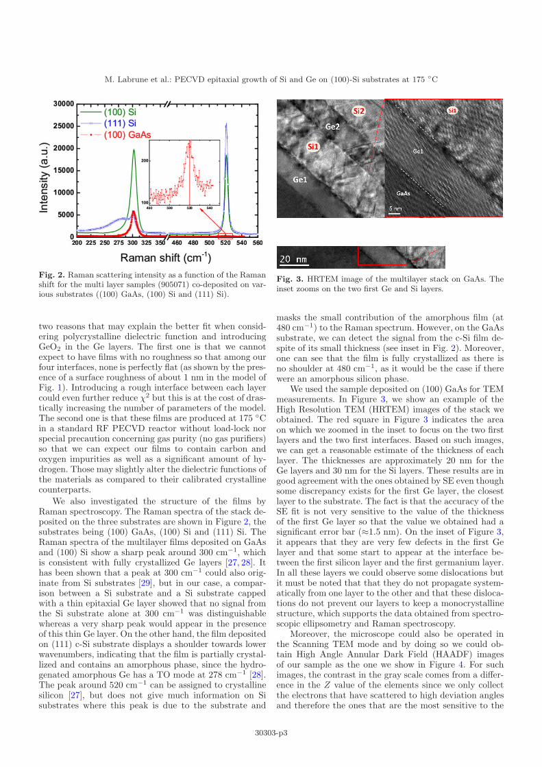
Fig. 3. HRTEM image of the multilayer stack on GaAs. Theinset zooms on the two first Ge and Si layers.
masks the small contribution of the amorphous film (at480 cm−1) to the Raman spectrum. However, on the GaAssubstrate, we can detect the signal from the c-Si film de-spite of its small thickness (see inset in Fig. 2). Moreover,one can see that the film is fully crystallized as there isno shoulder at 480 cm−1, as it would be the case if therewere an amorphous silicon phase.
We used the sample deposited on (100) GaAs for TEMmeasurements. In Figure 3, we show an example of theHigh Resolution TEM (HRTEM) images of the stack weobtained. The red square in Figure 3 indicates the areaon which we zoomed in the inset to focus on the two firstlayers and the two first interfaces. Based on such images,we can get a reasonable estimate of the thickness of eachlayer. The thicknesses are approximately 20 nm for theGe layers and 30 nm for the Si layers. These results are ingood agreement with the ones obtained by SE even thoughsome discrepancy exists for the first Ge layer, the closestlayer to the substrate. The fact is that the accuracy of theSE fit is not very sensitive to the value of the thicknessof the first Ge layer so that the value we obtained had asignificant error bar (≈1.5 nm). On the inset of Figure 3,it appears that they are very few defects in the first Gelayer and that some start to appear at the interface be-tween the first silicon layer and the first germanium layer.In all these layers we could observe some dislocations butit must be noted that that they do not propagate system-atically from one layer to the other and that these disloca-tions do not prevent our layers to keep a monocrystallinestructure, which supports the data obtained from spectro-scopic ellipsometry and Raman spectroscopy.
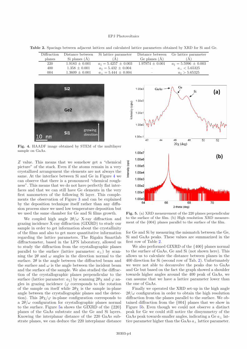
Moreover, the microscope could also be operated inthe Scanning TEM mode and by doing so we could ob-tain High Angle Annular Dark Field (HAADF) imagesof our sample as the one we show in Figure 4. For suchimages, the contrast in the gray scale comes from a differ-ence in the Z value of the elements since we only collectthe electrons that have scattered to high deviation anglesand therefore the ones that are the most sensitive to the
30303-p3
EPJ Photovoltaics
Table 2. Spacings between adjacent lattices and calculated lattice parameters obtained by XRD for Si and Ge.
Diffraction Distance between Si lattice parameter Distance between Ge lattice parameterplanes Si planes (A) (A) Ge planes (A) (A)220 1.9183 ± 0.001 a‖ = 5.4257 ± 0.003 1.97974 ± 0.001 a‖ = 5.5996 ± 0.003400 1.358 ± 0.001 a‖ = 5.432 ± 0.004 – a⊥ < 5.65325004 1.3609 ± 0.001 a⊥ = 5.444 ± 0.004 – a‖ > 5.65325
Fig. 4. HAADF image obtained by STEM of the multilayersample on GaAs.
Z value. This means that we somehow get a “chemicalpicture” of the stack. Even if the atoms remain in a verycrystallized arrangement the elements are not always thesame. At the interface between Si and Ge in Figure 4 wecan observe that there is a pronounced “chemical rough-ness”. This means that we do not have perfectly flat inter-faces and that we can still have Ge elements in the veryfirst nanometers of the following Si layer. This comple-ments the observation of Figure 3 and can be explainedby the deposition technique itself rather than any diffu-sion process since we used low temperature deposition butwe used the same chamber for Ge and Si films growth.
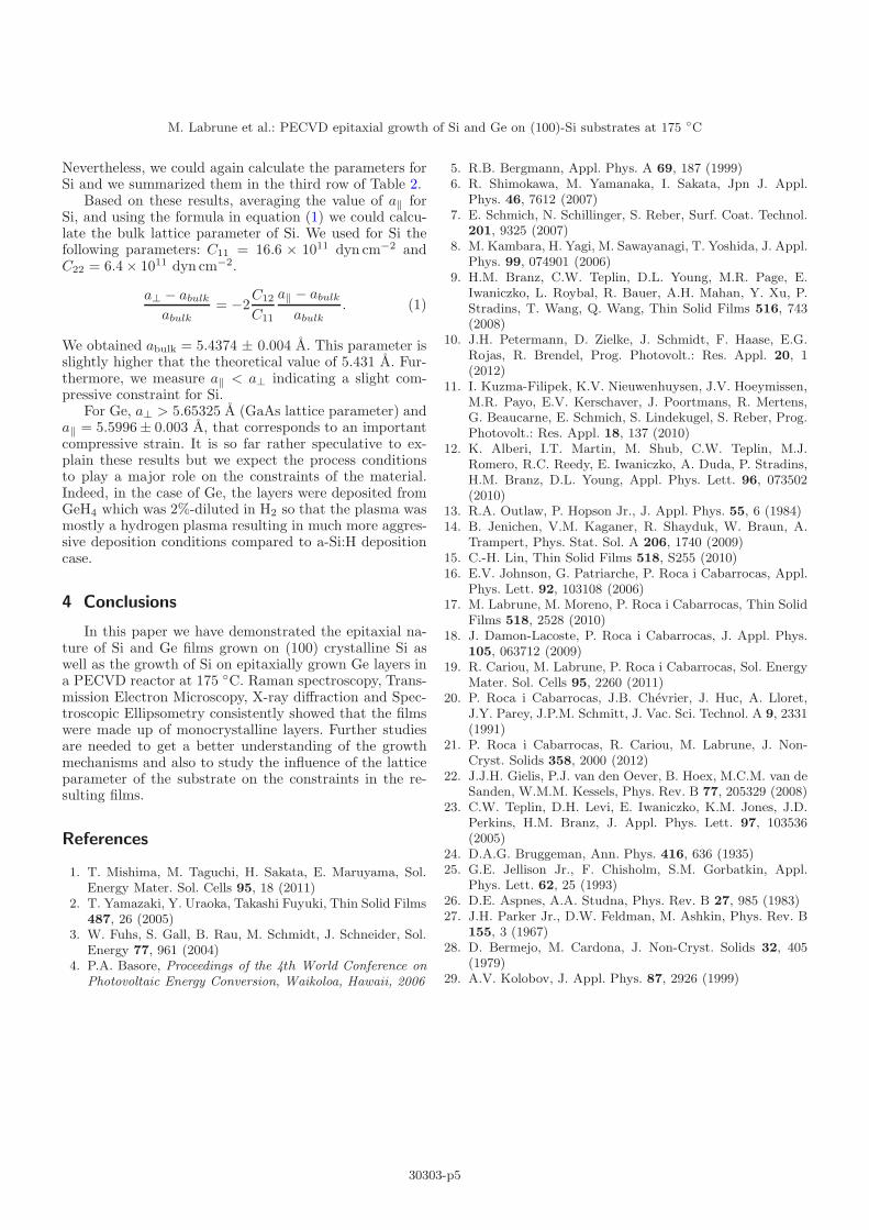
We coupled high angle 2θ/ω X-ray diffraction andgrazing incidence X-ray diffraction (GIXRD) to study oursample in order to get information about the crystallinityof the films and also to get more quantitative informationregarding the lattice parameters. The Rigaku Smartlabdiffractometer, based in the LPN laboratory, allowed usto study the diffraction from the crystallographic planesparallel to the surface (lattice parameter: a⊥) by scan-ning the 2θ and ω angles in the direction normal to thesurface. 2θ is the angle between the diffracted beam andthe surface and ω is the angle between the incident beamand the surface of the sample. We also studied the diffrac-tion of the crystallographic planes perpendicular to thesurface (lattice parameter: a‖) by scanning 2θχ and ϕ an-gles in grazing incidence (ϕ corresponds to the rotationof the sample on itself while 2θχ is the sample in-planeangle between the crystallographic planes and the detec-tion). This 2θχ/ϕ in-plane configuration corresponds toa 2θ/ω configuration for crystallographic planes normalto the surface. Figure 5a shows the GIXRD of the {220}planes of the GaAs substrate and the Ge and Si layers.Knowing the interplanar distance of the 220 GaAs sub-strate planes, we can deduce the 220 interplanar distance
Fig. 5. (a) XRD measurement of the 220 planes perpendicularto the surface of the film. (b) High resolution XRD measure-ment of the {004} planes parallel to the surface of the film.
for Ge and Si by measuring the mismatch between the Ge,Si and GaAs peaks. These values are summarized in thefirst row of Table 2.
We also performed GIXRD of the {400} planes normalto the surface of GaAs, Ge and Si (not shown here). Thisallows us to calculate the distance between planes in the400 direction for Si (second row of Tab. 2). Unfortunatelywe were not able to deconvolve the peaks due to GaAsand Ge but based on the fact the graph showed a shouldertowards higher angles around the 400 peak of GaAs, wecan assume that we have a lattice parameter lower thanthe one of GaAs.
Finally we operated the XRD set-up in the high angle2θ/ω configuration in order to obtain the high resolutiondiffraction from the planes parallel to the surface. We ob-tained diffraction from the {004} planes that we show inFigure 5b. Even though we could not observe a distinctpeak for Ge we could still notice the dissymmetry of theGaAs peak towards smaller angles, indicating a Ge a⊥ lat-tice parameter higher than the GaAs a⊥ lattice parameter.
30303-p4
M. Labrune et al.: PECVD epitaxial growth of Si and Ge on (100)-Si substrates at 175 ◦C
Nevertheless, we could again calculate the parameters forSi and we summarized them in the third row of Table 2.
Based on these results, averaging the value of a‖ forSi, and using the formula in equation (1) we could calcu-late the bulk lattice parameter of Si. We used for Si thefollowing parameters: C11 = 16.6 × 10¹¹ dyn cm−2 andC22 = 6.4 × 10¹¹ dyn cm−2.
a⊥ − abulk
abulk= −2
C12
C11
a‖ − abulk
abulk. (1)
We obtained abulk = 5.4374 ± 0.004 A. This parameter isslightly higher that the theoretical value of 5.431 A. Fur-thermore, we measure a‖ < a⊥ indicating a slight com-pressive constraint for Si.
For Ge, a⊥ > 5.65325 A (GaAs lattice parameter) anda‖ = 5.5996 ± 0.003 A, that corresponds to an importantcompressive strain. It is so far rather speculative to ex-plain these results but we expect the process conditionsto play a major role on the constraints of the material.Indeed, in the case of Ge, the layers were deposited fromGeH4 which was 2%-diluted in H2 so that the plasma wasmostly a hydrogen plasma resulting in much more aggres-sive deposition conditions compared to a-Si:H depositioncase.
4 Conclusions
In this paper we have demonstrated the epitaxial na-ture of Si and Ge films grown on (100) crystalline Si aswell as the growth of Si on epitaxially grown Ge layers ina PECVD reactor at 175 ◦C. Raman spectroscopy, Trans-mission Electron Microscopy, X-ray diffraction and Spec-troscopic Ellipsometry consistently showed that the filmswere made up of monocrystalline layers. Further studiesare needed to get a better understanding of the growthmechanisms and also to study the influence of the latticeparameter of the substrate on the constraints in the re-sulting films.
References
1. T. Mishima, M. Taguchi, H. Sakata, E. Maruyama, Sol.Energy Mater. Sol. Cells 95, 18 (2011)
2. T. Yamazaki, Y. Uraoka, Takashi Fuyuki, Thin Solid Films487, 26 (2005)
3. W. Fuhs, S. Gall, B. Rau, M. Schmidt, J. Schneider, Sol.Energy 77, 961 (2004)
4. P.A. Basore, Proceedings of the 4th World Conference onPhotovoltaic Energy Conversion, Waikoloa, Hawaii, 2006
5. R.B. Bergmann, Appl. Phys. A 69, 187 (1999)6. R. Shimokawa, M. Yamanaka, I. Sakata, Jpn J. Appl.
Phys. 46, 7612 (2007)7. E. Schmich, N. Schillinger, S. Reber, Surf. Coat. Technol.
201, 9325 (2007)8. M. Kambara, H. Yagi, M. Sawayanagi, T. Yoshida, J. Appl.
Phys. 99, 074901 (2006)9. H.M. Branz, C.W. Teplin, D.L. Young, M.R. Page, E.
Iwaniczko, L. Roybal, R. Bauer, A.H. Mahan, Y. Xu, P.Stradins, T. Wang, Q. Wang, Thin Solid Films 516, 743(2008)
10. J.H. Petermann, D. Zielke, J. Schmidt, F. Haase, E.G.Rojas, R. Brendel, Prog. Photovolt.: Res. Appl. 20, 1(2012)
11. I. Kuzma-Filipek, K.V. Nieuwenhuysen, J.V. Hoeymissen,M.R. Payo, E.V. Kerschaver, J. Poortmans, R. Mertens,G. Beaucarne, E. Schmich, S. Lindekugel, S. Reber, Prog.Photovolt.: Res. Appl. 18, 137 (2010)
12. K. Alberi, I.T. Martin, M. Shub, C.W. Teplin, M.J.Romero, R.C. Reedy, E. Iwaniczko, A. Duda, P. Stradins,H.M. Branz, D.L. Young, Appl. Phys. Lett. 96, 073502(2010)
13. R.A. Outlaw, P. Hopson Jr., J. Appl. Phys. 55, 6 (1984)14. B. Jenichen, V.M. Kaganer, R. Shayduk, W. Braun, A.
Trampert, Phys. Stat. Sol. A 206, 1740 (2009)15. C.-H. Lin, Thin Solid Films 518, S255 (2010)16. E.V. Johnson, G. Patriarche, P. Roca i Cabarrocas, Appl.
Phys. Lett. 92, 103108 (2006)17. M. Labrune, M. Moreno, P. Roca i Cabarrocas, Thin Solid
Films 518, 2528 (2010)18. J. Damon-Lacoste, P. Roca i Cabarrocas, J. Appl. Phys.
105, 063712 (2009)19. R. Cariou, M. Labrune, P. Roca i Cabarrocas, Sol. Energy
Mater. Sol. Cells 95, 2260 (2011)20. P. Roca i Cabarrocas, J.B. Chevrier, J. Huc, A. Lloret,
J.Y. Parey, J.P.M. Schmitt, J. Vac. Sci. Technol. A 9, 2331(1991)
21. P. Roca i Cabarrocas, R. Cariou, M. Labrune, J. Non-Cryst. Solids 358, 2000 (2012)
22. J.J.H. Gielis, P.J. van den Oever, B. Hoex, M.C.M. van deSanden, W.M.M. Kessels, Phys. Rev. B 77, 205329 (2008)
23. C.W. Teplin, D.H. Levi, E. Iwaniczko, K.M. Jones, J.D.Perkins, H.M. Branz, J. Appl. Phys. Lett. 97, 103536(2005)
24. D.A.G. Bruggeman, Ann. Phys. 416, 636 (1935)25. G.E. Jellison Jr., F. Chisholm, S.M. Gorbatkin, Appl.
Phys. Lett. 62, 25 (1993)26. D.E. Aspnes, A.A. Studna, Phys. Rev. B 27, 985 (1983)27. J.H. Parker Jr., D.W. Feldman, M. Ashkin, Phys. Rev. B
155, 3 (1967)28. D. Bermejo, M. Cardona, J. Non-Cryst. Solids 32, 405
(1979)29. A.V. Kolobov, J. Appl. Phys. 87, 2926 (1999)
30303-p5