Embed Size (px)
Citation preview
Application ReportSLAA530–March 2012
MSP430™ System-Level ESD Considerations........................................................................................................................ MSP430 Applications
ABSTRACT
System-Level ESD has become increasingly demanding with silicon technology scaling towards lowervoltages and the need for designing cost-effective and ultra-low power components. This applicationreport addresses three different ESD topics to help board designers and OEMs understand and designrobust system-level designs:
1. Component-level ESD testing and system-level ESD testing, their differences, and why component-level ESD rating does not ensure system-level robustness.
2. General design guidelines for system-level ESD protection at different levels including enclosures,cables, PCB layout, and on-board ESD protection devices.
3. Introduction to System Efficient ESD Design (SEED, which is a co-design methodology of on-boardand on-chip ESD protection to achieve system-level ESD robustness) with example simulations andtest results.
Two real-world system-level ESD protection design examples and their results are also discussed.
MSP430 is a trademark of Texas Instruments.All other trademarks are the property of their respective owners.
1SLAA530–March 2012 MSP430 System-Level ESD ConsiderationsSubmit Documentation Feedback
Copyright © 2012, Texas Instruments Incorporated
www.ti.com
Contents1 Introduction to ESD ......................................................................................................... 32 General System-Level ESD Design Guidelines ......................................................................... 93 System Efficient ESD Design (SEED) .................................................................................. 224 SEED-Based IEC Protection Design and Verification – Real World Example 1 .................................. 265 System-Level ESD Protection – Real World Example 2 ............................................................. 326 Summary ................................................................................................................... 337 References ................................................................................................................. 34Appendix A Modeling Using TLP Parameters ............................................................................... 35
List of Figures
1 Human Body Model (Similar to JEDEC JS-001 Specification)........................................................ 4
2 Charged Device Model (Similar to the JEDEC JESD22-C101 Specification)....................................... 5
3 ESD Test Bench for Powered Condition From IEC 61000-4-2 [1] ................................................... 6
4 Comparison of Standard HBM, CDM, and IEC Discharge Pulses ................................................... 8
5 Enclosure Scenarios ...................................................................................................... 10
6 Shielding LEDs ............................................................................................................ 11
7 Enclosure Opening Considerations ..................................................................................... 12
8 Enclosure Cable Considerations ........................................................................................ 12
9 Avoid Right-Angle Traces ................................................................................................ 13
10 Decoupling Basics......................................................................................................... 13
11 Example Crystal Layout .................................................................................................. 14
12 Example Layout With Solid Ground Plane ............................................................................. 15
13 Grounding Considerations For 2-Layer Board With No Dedicated Ground Plane................................ 15
14 Return Currents and Resulting Loop Area ............................................................................. 16
15 Example 2-Layer PCB Layout Showing Large Current Loop........................................................ 17
16 Example 2-Layer PCB Layout Showing More Continuous Ground Plane And Reduced Current Loop ....... 18
17 System-Level ESD Protection Using Series Resistors ............................................................... 20
18 Two-Stage System-Level ESD Protection [7].......................................................................... 23
19 IEC ESD Protection Design Schematic................................................................................. 25
20 SPICE Simulations ........................................................................................................ 26
21 I-V Characteristics for a Bidirectional ESD Protection Diode ........................................................ 27
22 SEED Method Simulation Schematic ................................................................................... 28
23 SEED Schematic and Simulation Results.............................................................................. 30
24 MSP430-Based Test Board Layout ..................................................................................... 31
25 MSP430-Based Real-Time Clock Test Boards ........................................................................ 32
26 Modeling TVS Device Using TLP Parameters......................................................................... 35
27 Modeling IC Interface Pin Using TLP Parameters .................................................................... 36
List of Tables
1 Comparison of IC-Level HBM and System-Level ESD Tests [2] ..................................................... 3
2 IEC 61000-4-2 Test Specifications [1].................................................................................... 7
3 System-Level ESD Performance - Real World Example 2 Results................................................. 32
2 MSP430 System-Level ESD Considerations SLAA530–March 2012Submit Documentation Feedback
Copyright © 2012, Texas Instruments Incorporated
www.ti.com Introduction to ESD
1 Introduction to ESD
Static charge is an unbalanced electrical charge at rest. When two non-conductive materials are rubbedtogether or separated, there is gain of electrons on the surface of one material and loss on the other; thisresults in an unbalanced electrical conditions known as static charge. The voltage to which an object canbe charged depends on the capacitance, following the law Q = CV. The human body can be charged toseveral kV. When this static charge moves from one surface to another, it is called ESD (ElectrostaticDischarge). ESD is a single-event rapid transfer of electrostatic charge between two objects that are atdifferent potentials. It can occur only when the voltage differential between the two objects is sufficientlyhigh to break down the dielectric strength of the medium separating them. The rapid movement of theelectrostatic charge generates current that damages or destroys gate oxide, metallization, and junctionswithin an integrated circuit (IC).
ESD can occur in any one of the four ways:
• Charged body touching an IC
• Charged IC touching a grounded surface or object
• Charged metallic tool touching an IC
• An electrostatic field inducing a voltage across a dielectric sufficient enough to break it down.
The coupling mechanisms in each of these cases are inductive, resistive, or capacitive. Creating an ESD-safe design is focused on minimizing ESD coupling by a combination of factors. To design an ESD robustproduct, it is important to understand that the ESD protection required at component or IC level and atsystem level are different.
Typically, silicon vendors design, test, and qualify their ICs according to industry standards to ensure nophysical damage occurs during IC production or during assembly onto PCBs. The Original EquipmentManufacturer (OEM) should design ESD protection at a system or board level and test according to theIEC 61000-4-2 [1] or ISO 10605 [6] system-level ESD standard. Table 1 summarizes key differencesbetween IC- or component-level standard HBM testing and system-level testing as required by IEC 61000-4-2 [1] and ISO 10605 [6] standards.
Table 1. Comparison of IC-Level HBM and System-Level ESD Tests [2]
Parameter IC-Level HBM Test System-Level ESD Test(ANSI/ESDA/JEDEC JS-001) [3] (IEC 61000-4-2 [1], ISO 10605 [6])
Stressed Pin Group Multitude of pin combinations Few special pins
Device Power Non-powered Powered and non-powered
Application specific using variousTest Methodology Standardized discharge models
Functional or application failure orFailure Signature Leakage or physical device damage physical device damage
Testing and Qualification Owned by Silicon vendor or component manufacturer System board designers or OEMs
Test Setup Commercial tester and sockets Application-specific board
Typical Qualification Goal 1 kV to 2 kV HBM 8 kV to 15 kV
Corresponding Peak Current 0.65 A to 1.3 A >20 A
ESD Environment Assembly and production processes End-user application, consumer product
The component-level ESD and the system-level ESD test requirements are different as they addressdifferent ESD environments. Also, the ESD current waveforms associated with the two tests differsignificantly in terms of peak current, duration, and total power. Therefore, to design an ESD robustsystem, it is important for the system board designers and OEMs to understand that system-level ESDprotection requirements are much different from IC-level ESD protection capabilities..
3SLAA530–March 2012 MSP430 System-Level ESD ConsiderationsSubmit Documentation Feedback
Copyright © 2012, Texas Instruments Incorporated
DUT
High-VoltageSupply
Charging Resistor 1.5-kW
100-pF
Introduction to ESD www.ti.com
1.1 Component-Level ESD Rating
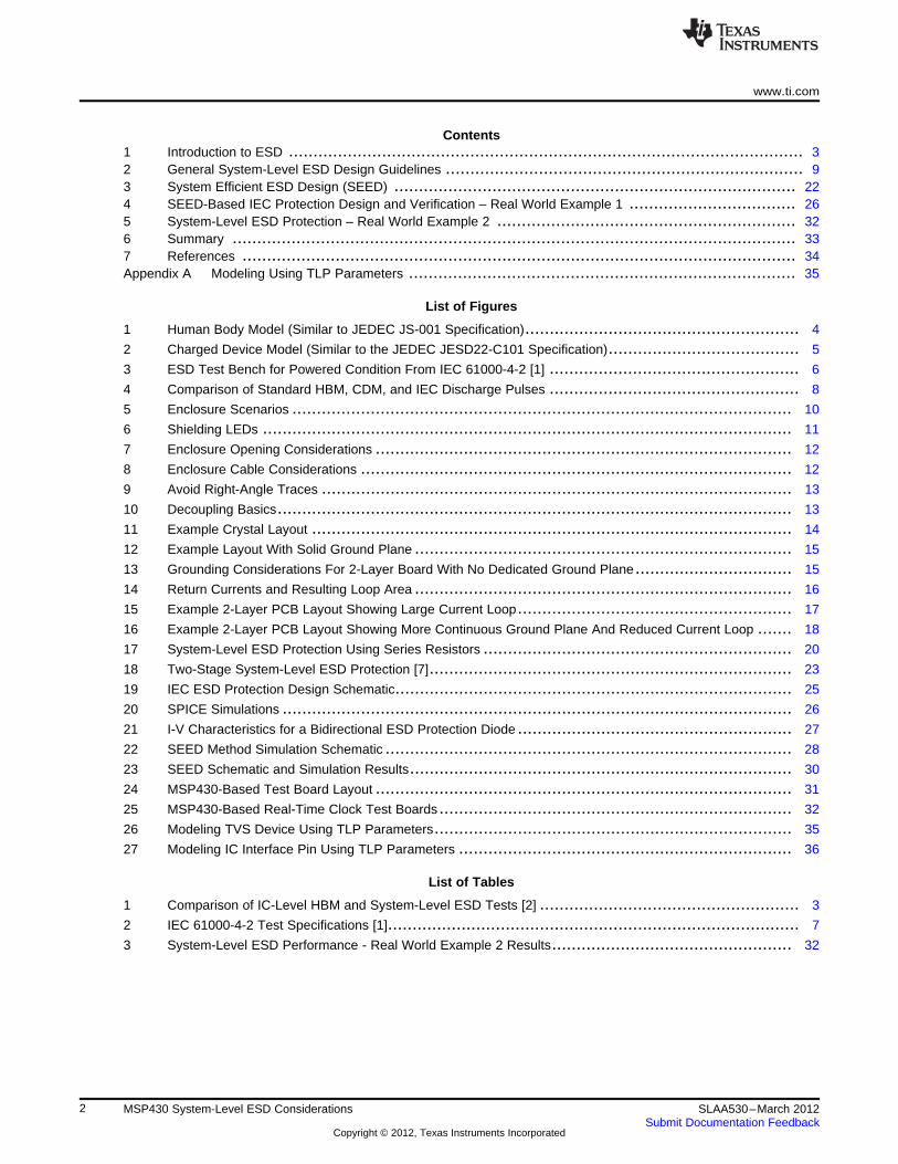
The ESD protection design for an IC package is known to be critical for safe production and handling. It iscommonly understood and accepted that this protection design is expected to meet or exceed the requiredESD specification when these ICs are handled in an ESD-safe area, also known as ESD Protected Area(EPA) [1]. The ESD protection strategy for ICs involves discharging of the ESD events that might occur onany pin of the package that is exposed to its environment. The component-level ESD protection shouldconsider the two basic ESD models defined for ICs: Human Body Model (HBM) and Charged DeviceModel (CDM).
The ESD protection circuitry within MSP430™ ICs is designed based on device technology, IC pinfunctionalities for different applications, power pins, and so on. The protection elements are firstcharacterized and analyzed for effectiveness using test chips. Simulations and automated checks areused, where appropriate, to ensure effectiveness of the protection circuitry and check for its compatibilitywith the pin it is designed to protect.
Typical MSP430 devices are tested and qualified to the following industry-standard ESD ratings.
1.1.1 Human Body Model (HBM)
The HBM simulates the ESD event in which a human body discharges the accumulated electrostaticcharge by touching an IC that is at a different potential. In a simple approximation, it is modeled by acharged 100-pF capacitor and a 1.5-kΩ discharging resistor, similar to the JEDEC JS-001 specification [3](see Figure 1).
Figure 1. Human Body Model (Similar to JEDEC JS-001 Specification)
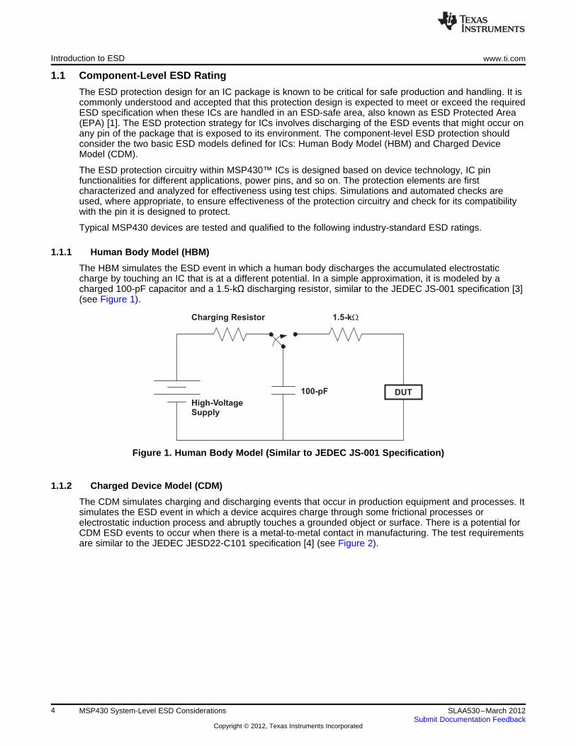
1.1.2 Charged Device Model (CDM)
The CDM simulates charging and discharging events that occur in production equipment and processes. Itsimulates the ESD event in which a device acquires charge through some frictional processes orelectrostatic induction process and abruptly touches a grounded object or surface. There is a potential forCDM ESD events to occur when there is a metal-to-metal contact in manufacturing. The test requirementsare similar to the JEDEC JESD22-C101 specification [4] (see Figure 2).
4 MSP430 System-Level ESD Considerations SLAA530–March 2012Submit Documentation Feedback
Copyright © 2012, Texas Instruments Incorporated
High-VoltageSupply
DUT
Charging Resistor
300 MW DischargingProbe
www.ti.com Introduction to ESD
Figure 2. Charged Device Model (Similar to the JEDEC JESD22-C101 Specification)
NOTE: These component-level ESD standards apply to unpowered devices and are an indicator ofdevice susceptibility to ESD events in a manufacturing environment. Texas Instruments doesnot ensure system-level ESD ratings such as IEC 61000-4-2 for the MSP430 family ofdevices. For system-level ESD protection guidelines and recommendations, see the followingsection.
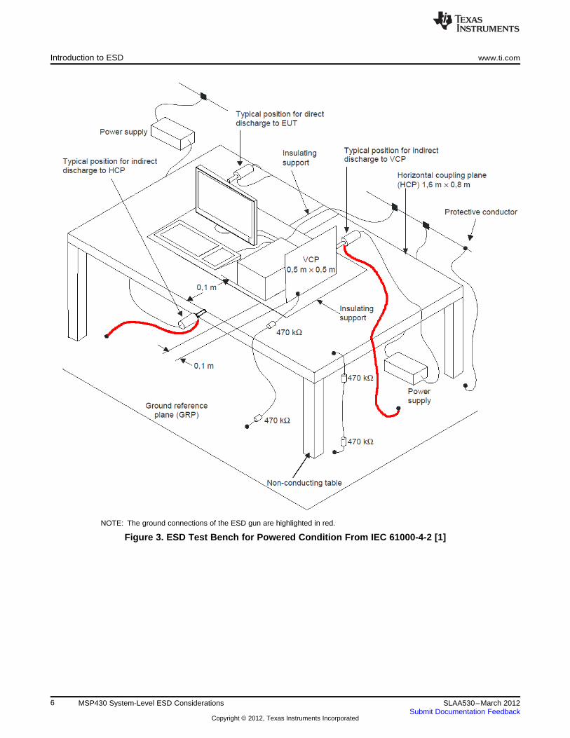
1.2 System-Level ESD Rating
Typically in ESD protected areas (EPA), the ESD voltage levels are low due to ESD-control measures asstandardized by ANSI/ESD S20.20 [13] and IEC 61340 [14] that are followed world-wide during assembly,packaging, and other production processes. The same cannot be assured when the end-product shipsand reaches the hands of the customer. A consumer product deployed to the field is usually handledoutside of an EPA and can be subjected to higher-voltage ESD strikes.
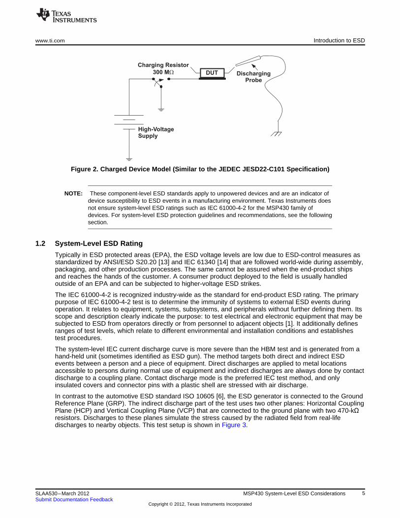
The IEC 61000-4-2 is recognized industry-wide as the standard for end-product ESD rating. The primarypurpose of IEC 61000-4-2 test is to determine the immunity of systems to external ESD events duringoperation. It relates to equipment, systems, subsystems, and peripherals without further defining them. Itsscope and description clearly indicate the purpose: to test electrical and electronic equipment that may besubjected to ESD from operators directly or from personnel to adjacent objects [1]. It additionally definesranges of test levels, which relate to different environmental and installation conditions and establishestest procedures.
The system-level IEC current discharge curve is more severe than the HBM test and is generated from ahand-held unit (sometimes identified as ESD gun). The method targets both direct and indirect ESDevents between a person and a piece of equipment. Direct discharges are applied to metal locationsaccessible to persons during normal use of equipment and indirect discharges are always done by contactdischarge to a coupling plane. Contact discharge mode is the preferred IEC test method, and onlyinsulated covers and connector pins with a plastic shell are stressed with air discharge.
In contrast to the automotive ESD standard ISO 10605 [6], the ESD generator is connected to the GroundReference Plane (GRP). The indirect discharge part of the test uses two other planes: Horizontal CouplingPlane (HCP) and Vertical Coupling Plane (VCP) that are connected to the ground plane with two 470-kΩresistors. Discharges to these planes simulate the stress caused by the radiated field from real-lifedischarges to nearby objects. This test setup is shown in Figure 3.
5SLAA530–March 2012 MSP430 System-Level ESD ConsiderationsSubmit Documentation Feedback
Copyright © 2012, Texas Instruments Incorporated
Introduction to ESD www.ti.com
NOTE: The ground connections of the ESD gun are highlighted in red.
Figure 3. ESD Test Bench for Powered Condition From IEC 61000-4-2 [1]
6 MSP430 System-Level ESD Considerations SLAA530–March 2012Submit Documentation Feedback
Copyright © 2012, Texas Instruments Incorporated
www.ti.com Introduction to ESD
Table 2 lists the IEC 61000-4-2 test specifications.
Table 2. IEC 61000-4-2 Test Specifications [1]
Test Parameter IEC 61000-4-2
Discharge Type Contact Air
Output Voltage 2 kV to 8 kV 2 kV to 15 kV
Interval Time Minimum 1s
Polarity at Each Stress Voltage Level Positive and negative
Network Capacitance 150 pF
Network Resistance 330 ΩNumber of Discharge Pulses Minimum 10
Test Condition Powered
When testing a system to this or similar system-level standards, the end-products are required to remainfunctional in the presence of or following an ESD event. The IEC specified system-level failure criteriaclassifications are as follows:
• Normal performance within limits specified by the manufacturer.
• Temporary loss of function or degradation of performance that ceases after the disturbance ceases.Equipment under test recovers its normal performance without operator intervention.
• Temporary loss of function or degradation of performance. Recovery requires operator intervention.
• Temporary loss of function or degradation of performance which is not recoverable, caused by damageto hardware or software, or loss of data.
It is clear that most of above categories don't relate to physical device damage, but rather system upsets.The acceptance criterion for any particular system or application is specific to that case. Therefore, theboard designers and OEMs should handle the system-level ESD robustness by taking necessaryprecautions to prevent or minimize ESD coupling into the system or device (either directly through devicepins or via connected cables) that develop errors on signal traces or damages the device itself.
The later sections in this document highlight a few general guidelines that can help create an ESD-robustsystem solution. Too often ESD testing is carried out as an after-thought and board designers and OEMsfind themselves failing IEC-type tests because they have not taken the necessary precautions whiledesigning their application. Hence, board designers and OEMs are encouraged to see this document andnumerous published materials available with regards to ESD safety before starting their design.
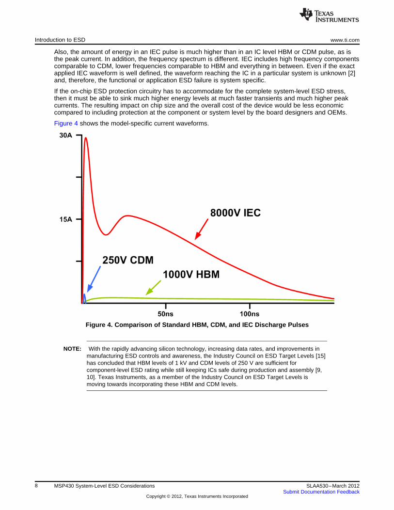
1.3 ESD Waveforms
When an electrostatically charged object is discharged, the resultant discharge current consists of a veryfast edge followed by a comparatively slow bulk discharge curve. The current discharge curves associatedwith the different component-level ESD models (HBM, CDM) and the system level models (IEC 64000-4-2) differ significantly.
The standard HBM current waveform has a specified rise time between 2 and 10 ns, while the CDM risetime is typically in the range of 50 to 500 ps, depending on the effective device size and capacitance, andthe IEC initial pulse has a rise time between 0.6 to 1 ns, while the secondary larger total energy pulse hasa rise time between 10 and 20 ns. These current discharge differences are critical to the effectiveness ofon-chip protection structures in terms of hardware failure or physical device damage. Most on-chip ESDprotection elements are dependent on the rise time of the initial pulse for turn-on response, in addition tothe total power and peak current handling capability. Thus, they can be expected to perform differently fordifferent model stresses [2]. This implies that the on-chip ESD protection that is designed to cater to IC-level ESD standards (like HBM, CDM) cannot accommodate for ESD stress at the system level to ensureprevention of physical device damage and other system upsets; and this should be handled at the systemlevel by the board designer or OEMs.
7SLAA530–March 2012 MSP430 System-Level ESD ConsiderationsSubmit Documentation Feedback
Copyright © 2012, Texas Instruments Incorporated
Introduction to ESD www.ti.com
Also, the amount of energy in an IEC pulse is much higher than in an IC level HBM or CDM pulse, as isthe peak current. In addition, the frequency spectrum is different. IEC includes high frequency componentscomparable to CDM, lower frequencies comparable to HBM and everything in between. Even if the exactapplied IEC waveform is well defined, the waveform reaching the IC in a particular system is unknown [2]and, therefore, the functional or application ESD failure is system specific.
If the on-chip ESD protection circuitry has to accommodate for the complete system-level ESD stress,then it must be able to sink much higher energy levels at much faster transients and much higher peakcurrents. The resulting impact on chip size and the overall cost of the device would be less economiccompared to including protection at the component or system level by the board designers and OEMs.
Figure 4 shows the model-specific current waveforms.
Figure 4. Comparison of Standard HBM, CDM, and IEC Discharge Pulses
NOTE: With the rapidly advancing silicon technology, increasing data rates, and improvements inmanufacturing ESD controls and awareness, the Industry Council on ESD Target Levels [15]has concluded that HBM levels of 1 kV and CDM levels of 250 V are sufficient forcomponent-level ESD rating while still keeping ICs safe during production and assembly [9,10]. Texas Instruments, as a member of the Industry Council on ESD Target Levels ismoving towards incorporating these HBM and CDM levels.
8 MSP430 System-Level ESD Considerations SLAA530–March 2012Submit Documentation Feedback
Copyright © 2012, Texas Instruments Incorporated
www.ti.com General System-Level ESD Design Guidelines
2 General System-Level ESD Design Guidelines
System-level ESD protection strategies depend strongly on physical design, operational requirements andoverall cost of the end-product. There are different disciplines of protection that can be considered tominimize ESD coupling into the system. A robust ESD system design involves factoring multiple elementssuch as:
• Enclosure
• PCB design and layout
• ESD ground paths
• On-board ESD protection devices
• System wiring and interconnects
• Software design
• ESD testing
The key to an ESD-robust system design is to consider the effects of ESD in the system early on duringdesign and development of the board by following ESD-immune design guidelines. ESD testingthroughout development helps identify and fix weak ESD spots in the system through different stages.
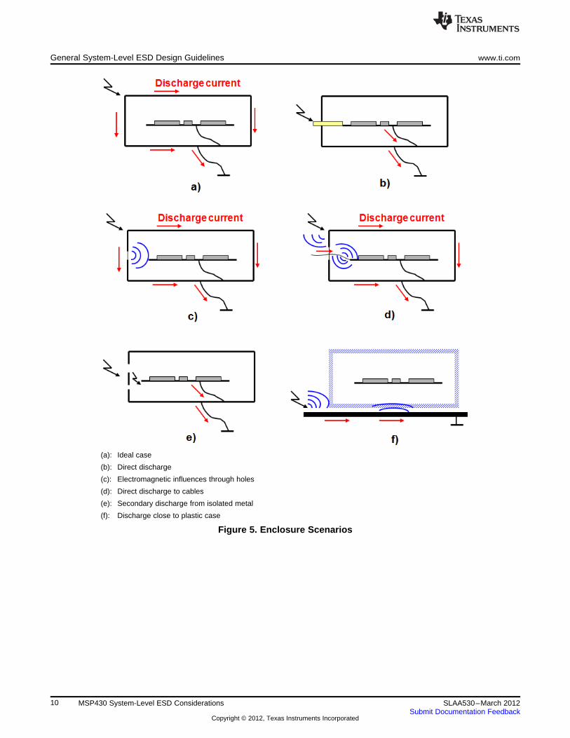
2.1 Enclosures
Identifying the ESD entry points in the system and designing enclosures such that any direct or indirectelectrostatic discharge into the system is minimized, is key to any system-level ESD protection design.Figure 5 shows various enclosure cases and respective ESD entry scenarios.
Figure 5(a) represents an ideal case where the conductive enclosure is properly shielded and grounded;ESD does not influence the system at all. This is an ideal case, but it is not applicable in most systems.
Figure 5(b) represents the direct discharge case where a conductive block in the system is protruding outof the enclosure and the electrostatic discharge gets coupled onto the system right through this block. Agood design would make sure that the conductive block penetrating out of the enclosure is properlyshielded to minimize ESD coupling.
Figure 5(c) represents the indirect discharge case where the electromagnetic fields that are generatedenter the system through the enclosure holes. These electromagnetic fields can couple to internal circuitsor wires and propagate through the system. Providing sufficient air gap between the enclosure holes andthe electronics within the enclosure can help minimize this coupling effect.
Figure 5(d) represents direct discharge to cables that in turn generate electromagnetic fields in thesystem. See Section 2.1.2 for recommended design guidelines.
Figure 5(e) represents secondary discharge from isolated metal bracket or panel that gets coupled to thesystem. See Section 2.1.1 for recommended design guidelines.
Figure 5(f) represents electrostatic discharge close to a plastic enclosure that generates anelectromagnetic field. Keeping sufficient air gap between the non-conductive enclosure and the electronicswithin the enclosure can help minimize electromagnetic noise coupling into the system.
9SLAA530–March 2012 MSP430 System-Level ESD ConsiderationsSubmit Documentation Feedback
Copyright © 2012, Texas Instruments Incorporated
General System-Level ESD Design Guidelines www.ti.com
(a): Ideal case
(b): Direct discharge
(c): Electromagnetic influences through holes
(d): Direct discharge to cables
(e): Secondary discharge from isolated metal
(f): Discharge close to plastic case
Figure 5. Enclosure Scenarios
10 MSP430 System-Level ESD Considerations SLAA530–March 2012Submit Documentation Feedback
Copyright © 2012, Texas Instruments Incorporated
www.ti.com General System-Level ESD Design Guidelines
2.1.1 Enclosure Openings
The following are general enclosure guidelines that can help to minimize ESD and EMI coupling onto thesystem (a PCB, in this case):
• Provide direct ground path to conductive enclosures to minimize ESD coupling into the system. Thedirect ground path should be short with a low inductance.
• Choosing plastic and other non-conductive enclosures, air space and insulation can prevent ESD arcsfrom penetrating inside the system.
• Keep sufficient air gap between points on the enclosure that are susceptible to ESD (includingventilation holes, mounting holes, seams, and so on) and the PCB.
• Choose switches and user controls with plastic shafts or cover metal shafts with plastic knobs
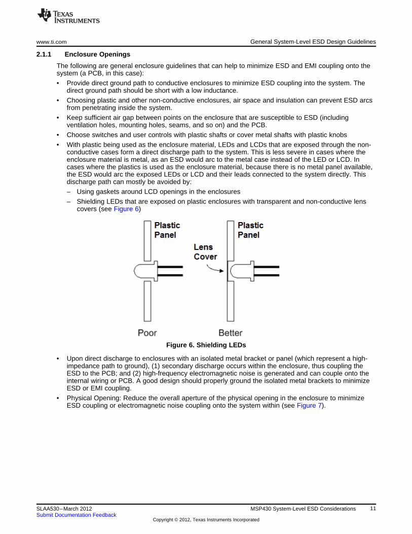
• With plastic being used as the enclosure material, LEDs and LCDs that are exposed through the non-conductive cases form a direct discharge path to the system. This is less severe in cases where theenclosure material is metal, as an ESD would arc to the metal case instead of the LED or LCD. Incases where the plastics is used as the enclosure material, because there is no metal panel available,the ESD would arc the exposed LEDs or LCD and their leads connected to the system directly. Thisdischarge path can mostly be avoided by:
– Using gaskets around LCD openings in the enclosures
– Shielding LEDs that are exposed on plastic enclosures with transparent and non-conductive lenscovers (see Figure 6)
Figure 6. Shielding LEDs
• Upon direct discharge to enclosures with an isolated metal bracket or panel (which represent a high-impedance path to ground), (1) secondary discharge occurs within the enclosure, thus coupling theESD to the PCB; and (2) high-frequency electromagnetic noise is generated and can couple onto theinternal wiring or PCB. A good design should properly ground the isolated metal brackets to minimizeESD or EMI coupling.
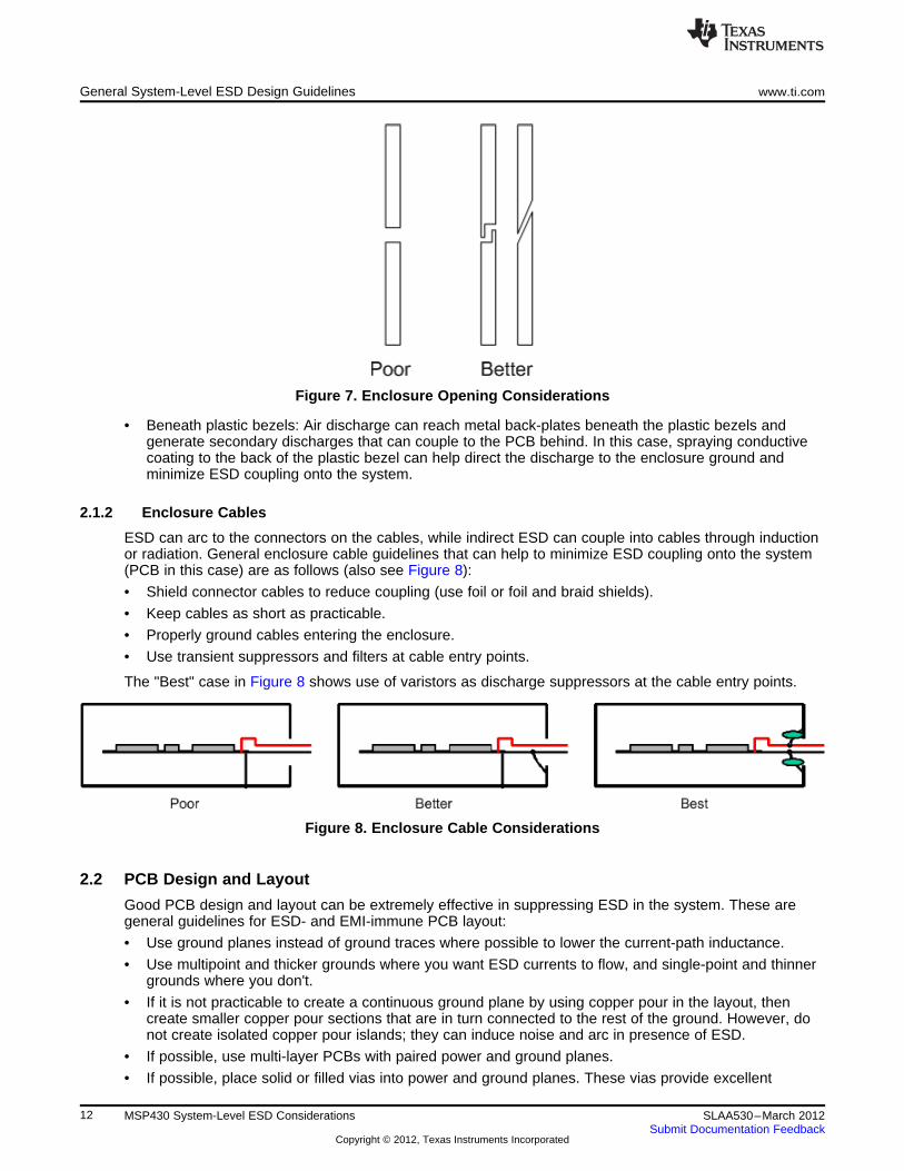
• Physical Opening: Reduce the overall aperture of the physical opening in the enclosure to minimizeESD coupling or electromagnetic noise coupling onto the system within (see Figure 7).
11SLAA530–March 2012 MSP430 System-Level ESD ConsiderationsSubmit Documentation Feedback
Copyright © 2012, Texas Instruments Incorporated
General System-Level ESD Design Guidelines www.ti.com
Figure 7. Enclosure Opening Considerations
• Beneath plastic bezels: Air discharge can reach metal back-plates beneath the plastic bezels andgenerate secondary discharges that can couple to the PCB behind. In this case, spraying conductivecoating to the back of the plastic bezel can help direct the discharge to the enclosure ground andminimize ESD coupling onto the system.
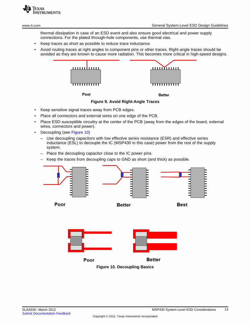
2.1.2 Enclosure Cables
ESD can arc to the connectors on the cables, while indirect ESD can couple into cables through inductionor radiation. General enclosure cable guidelines that can help to minimize ESD coupling onto the system(PCB in this case) are as follows (also see Figure 8):
• Shield connector cables to reduce coupling (use foil or foil and braid shields).
• Keep cables as short as practicable.
• Properly ground cables entering the enclosure.
• Use transient suppressors and filters at cable entry points.
The "Best" case in Figure 8 shows use of varistors as discharge suppressors at the cable entry points.
Figure 8. Enclosure Cable Considerations
2.2 PCB Design and Layout
Good PCB design and layout can be extremely effective in suppressing ESD in the system. These aregeneral guidelines for ESD- and EMI-immune PCB layout:
• Use ground planes instead of ground traces where possible to lower the current-path inductance.
• Use multipoint and thicker grounds where you want ESD currents to flow, and single-point and thinnergrounds where you don't.
• If it is not practicable to create a continuous ground plane by using copper pour in the layout, thencreate smaller copper pour sections that are in turn connected to the rest of the ground. However, donot create isolated copper pour islands; they can induce noise and arc in presence of ESD.
• If possible, use multi-layer PCBs with paired power and ground planes.
• If possible, place solid or filled vias into power and ground planes. These vias provide excellent
12 MSP430 System-Level ESD Considerations SLAA530–March 2012Submit Documentation Feedback
Copyright © 2012, Texas Instruments Incorporated
www.ti.com General System-Level ESD Design Guidelines
thermal dissipation in case of an ESD event and also ensure good electrical and power supplyconnections. For the plated through-hole components, use thermal vias.
• Keep traces as short as possible to reduce trace inductance.
• Avoid routing traces at right angles to component pins or other traces. Right angle traces should beavoided as they are known to cause more radiation. This becomes more critical in high-speed designs.
Figure 9. Avoid Right-Angle Traces
• Keep sensitive signal traces away from PCB edges.
• Place all connectors and external wires on one edge of the PCB.
• Place ESD susceptible circuitry at the center of the PCB (away from the edges of the board, externalwires, connectors and power).
• Decoupling (see Figure 10)
– Use decoupling capacitors with low effective series resistance (ESR) and effective seriesinductance (ESL) to decouple the IC (MSP430 in this case) power from the rest of the supplysystem.
– Place the decoupling capacitor close to the IC power pins.
– Keep the traces from decoupling caps to GND as short (and thick) as possible.
Figure 10. Decoupling Basics
13SLAA530–March 2012 MSP430 System-Level ESD ConsiderationsSubmit Documentation Feedback
Copyright © 2012, Texas Instruments Incorporated
General System-Level ESD Design Guidelines www.ti.com
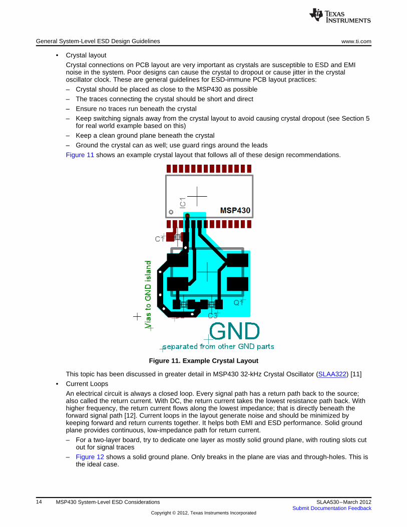
• Crystal layout
Crystal connections on PCB layout are very important as crystals are susceptible to ESD and EMInoise in the system. Poor designs can cause the crystal to dropout or cause jitter in the crystaloscillator clock. These are general guidelines for ESD-immune PCB layout practices:
– Crystal should be placed as close to the MSP430 as possible
– The traces connecting the crystal should be short and direct
– Ensure no traces run beneath the crystal
– Keep switching signals away from the crystal layout to avoid causing crystal dropout (see Section 5for real world example based on this)
– Keep a clean ground plane beneath the crystal
– Ground the crystal can as well; use guard rings around the leads
Figure 11 shows an example crystal layout that follows all of these design recommendations.
Figure 11. Example Crystal Layout
This topic has been discussed in greater detail in MSP430 32-kHz Crystal Oscillator (SLAA322) [11]
• Current Loops
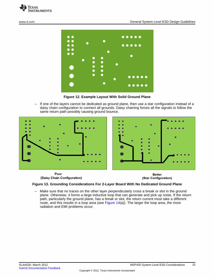
An electrical circuit is always a closed loop. Every signal path has a return path back to the source;also called the return current. With DC, the return current takes the lowest resistance path back. Withhigher frequency, the return current flows along the lowest impedance; that is directly beneath theforward signal path [12]. Current loops in the layout generate noise and should be minimized bykeeping forward and return currents together. It helps both EMI and ESD performance. Solid groundplane provides continuous, low-impedance path for return current.
– For a two-layer board, try to dedicate one layer as mostly solid ground plane, with routing slots cutout for signal traces
– Figure 12 shows a solid ground plane. Only breaks in the plane are vias and through-holes. This isthe ideal case.
14 MSP430 System-Level ESD Considerations SLAA530–March 2012Submit Documentation Feedback
Copyright © 2012, Texas Instruments Incorporated
www.ti.com General System-Level ESD Design Guidelines
Figure 12. Example Layout With Solid Ground Plane
– If one of the layers cannot be dedicated as ground plane, then use a star configuration instead of adaisy chain configuration to connect all grounds. Daisy chaining forces all the signals to follow thesame return path possibly causing ground bounce.
Figure 13. Grounding Considerations For 2-Layer Board With No Dedicated Ground Plane
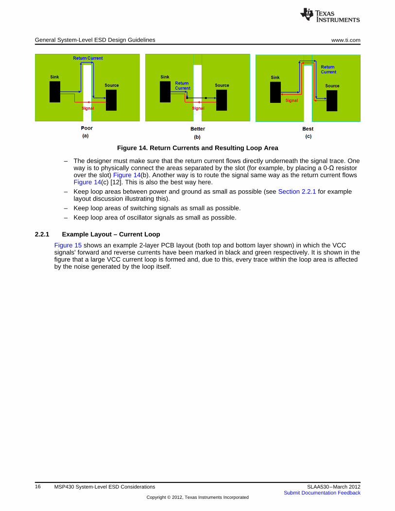
– Make sure that no traces on the other layer perpendicularly cross a break or slot in the groundplane. Otherwise, it forms a large inductive loop that can generate and pick up noise. If the returnpath, particularly the ground plane, has a break or slot, the return current must take a differentroute, and this results in a loop area (see Figure 14(a)). The larger the loop area, the moreradiation and EMI problems occur.
15SLAA530–March 2012 MSP430 System-Level ESD ConsiderationsSubmit Documentation Feedback
Copyright © 2012, Texas Instruments Incorporated
General System-Level ESD Design Guidelines www.ti.com
Figure 14. Return Currents and Resulting Loop Area
– The designer must make sure that the return current flows directly underneath the signal trace. Oneway is to physically connect the areas separated by the slot (for example, by placing a 0-Ω resistorover the slot) Figure 14(b). Another way is to route the signal same way as the return current flowsFigure 14(c) [12]. This is also the best way here.
– Keep loop areas between power and ground as small as possible (see Section 2.2.1 for examplelayout discussion illustrating this).
– Keep loop areas of switching signals as small as possible.
– Keep loop area of oscillator signals as small as possible.
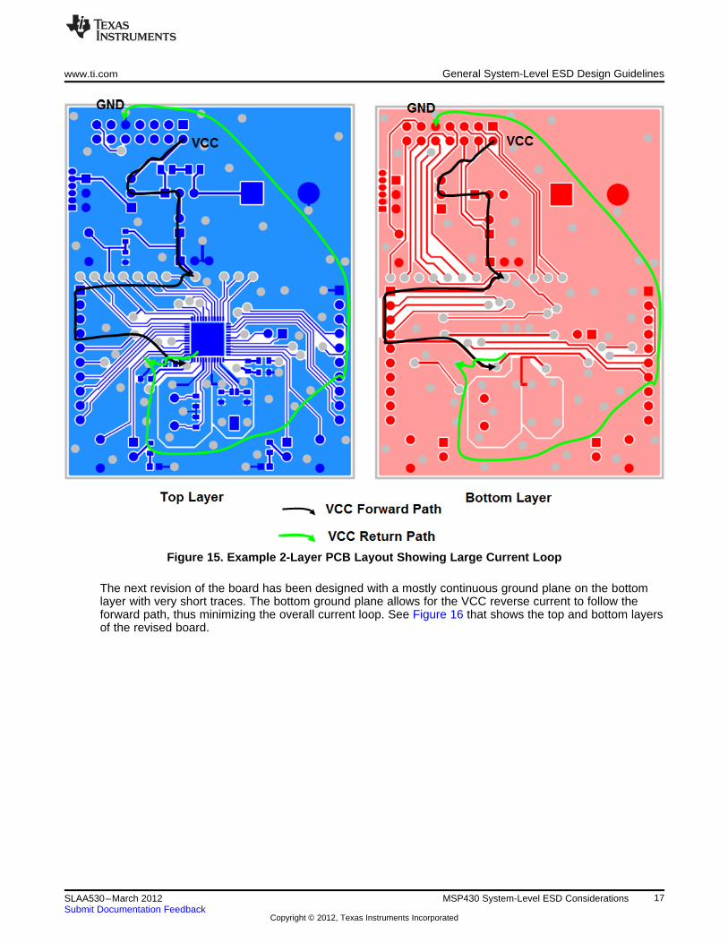
2.2.1 Example Layout – Current Loop
Figure 15 shows an example 2-layer PCB layout (both top and bottom layer shown) in which the VCCsignals' forward and reverse currents have been marked in black and green respectively. It is shown in thefigure that a large VCC current loop is formed and, due to this, every trace within the loop area is affectedby the noise generated by the loop itself.
16 MSP430 System-Level ESD Considerations SLAA530–March 2012Submit Documentation Feedback
Copyright © 2012, Texas Instruments Incorporated
www.ti.com General System-Level ESD Design Guidelines
Figure 15. Example 2-Layer PCB Layout Showing Large Current Loop
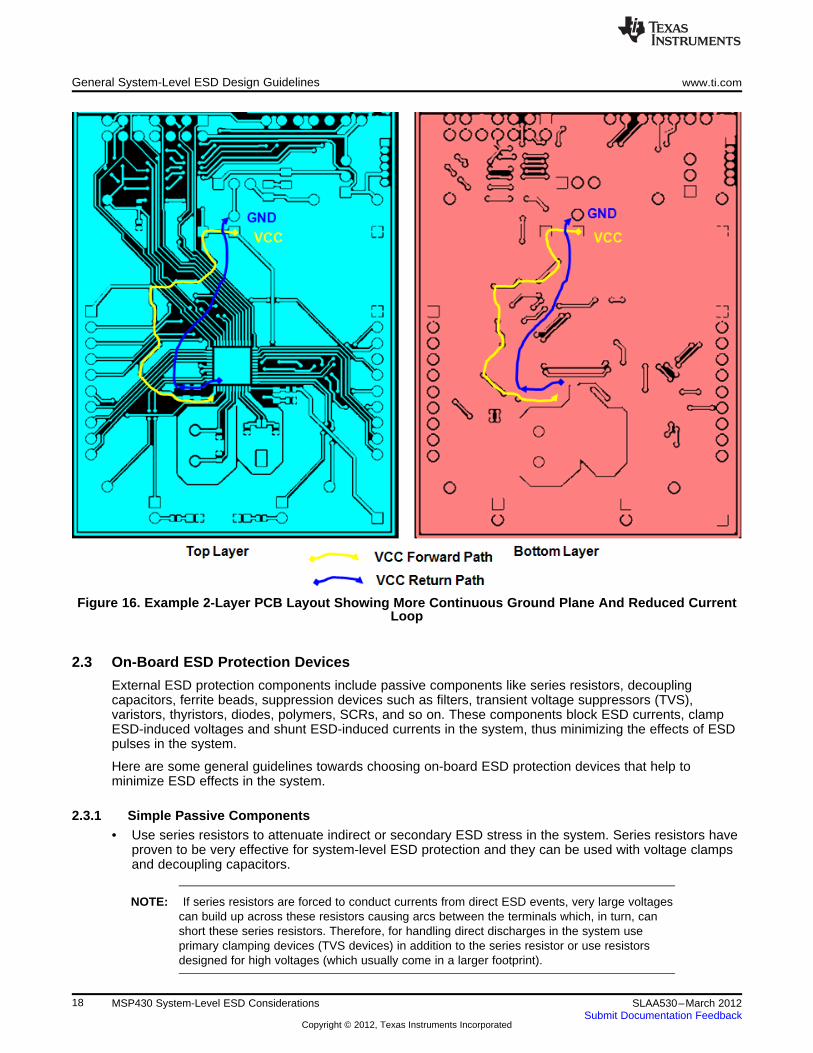
The next revision of the board has been designed with a mostly continuous ground plane on the bottomlayer with very short traces. The bottom ground plane allows for the VCC reverse current to follow theforward path, thus minimizing the overall current loop. See Figure 16 that shows the top and bottom layersof the revised board.
17SLAA530–March 2012 MSP430 System-Level ESD ConsiderationsSubmit Documentation Feedback
Copyright © 2012, Texas Instruments Incorporated
General System-Level ESD Design Guidelines www.ti.com
Figure 16. Example 2-Layer PCB Layout Showing More Continuous Ground Plane And Reduced CurrentLoop
2.3 On-Board ESD Protection Devices
External ESD protection components include passive components like series resistors, decouplingcapacitors, ferrite beads, suppression devices such as filters, transient voltage suppressors (TVS),varistors, thyristors, diodes, polymers, SCRs, and so on. These components block ESD currents, clampESD-induced voltages and shunt ESD-induced currents in the system, thus minimizing the effects of ESDpulses in the system.
Here are some general guidelines towards choosing on-board ESD protection devices that help tominimize ESD effects in the system.
2.3.1 Simple Passive Components• Use series resistors to attenuate indirect or secondary ESD stress in the system. Series resistors have
proven to be very effective for system-level ESD protection and they can be used with voltage clampsand decoupling capacitors.
NOTE: If series resistors are forced to conduct currents from direct ESD events, very large voltagescan build up across these resistors causing arcs between the terminals which, in turn, canshort these series resistors. Therefore, for handling direct discharges in the system useprimary clamping devices (TVS devices) in addition to the series resistor or use resistorsdesigned for high voltages (which usually come in a larger footprint).
18 MSP430 System-Level ESD Considerations SLAA530–March 2012Submit Documentation Feedback
Copyright © 2012, Texas Instruments Incorporated
www.ti.com General System-Level ESD Design Guidelines
• Use capacitors to provide simple decoupling. Choose capacitors with high-voltage rating, high resonantfrequency, low resistance (ESR), and low inductance (ESL). Minimize leads and trace lengthsconnecting the capacitors on the PCB.
• Use LC filters to block transients and EMI entering or exiting the system.
• Use ferrite beads to attenuate EMI and ESD.
These passive components should be placed as close as possible to the potential ESD stress points in thelayout
NOTE: Small SMD passive components usually do not provide good protection against direct 8-kVIEC pulses but they can be used to protect against secondary pulses in the system [2].
2.3.2 ESD Suppression Devices• Identify the maximum capacitance that can be applied to signal lines in the system and place
appropriate filters or TVS on sensitive signals (like resets, interrupts, edge triggered signals, and soon)
• Place filters or transient suppressors on off-board receivers and drivers for cables that are susceptibleto direct discharge (including signals that enter opto-isolators)
• Choose protection components for the system based on clamping voltage levels achievable, break-down voltage, response time, capacitance, dynamic resistance and ability to withstand multiple ESDstrikes. Texas Instruments offers a wide range of ESD and EMI protection devices and solutions; formore information regarding the ESD and EMI protection product portfolio, see Reference [5].
TVS Diodes
TVS diodes have lower capacitance and lower dynamic resistance values compared to other transientsuppression devices. They demonstrate high ESD multi-strike absorption capability; that is, once the ESDstrike is absorbed, the protection device returns to its high-impedance state very quickly. These devicesoffer very low clamping and breakdown voltages and have excellent response times.
Varistors
When an ESD event occurs, the varistor resistance changes from a very high standby value to a very lowconducting value, thus absorbing the ESD energy and limiting ESD-induced voltages. Varistors typicallyhave trigger voltages over 50 V, clamping voltages over 100 V, and a dynamic resistance over 20 Ω (afterturn on) [2]. They feature lower capacitance but have significant leakage currents after an ESD stress.
Polymer
These devices are similar to varistors in operation but have very low capacitance (0.05 to 1 pF) makingthem a good fit for high-frequency applications. The breakdown voltages are higher (compared tovaristors) and have lower endurance to multiple ESD strikes.
2.3.3 ESD Protection Using Series Resistor
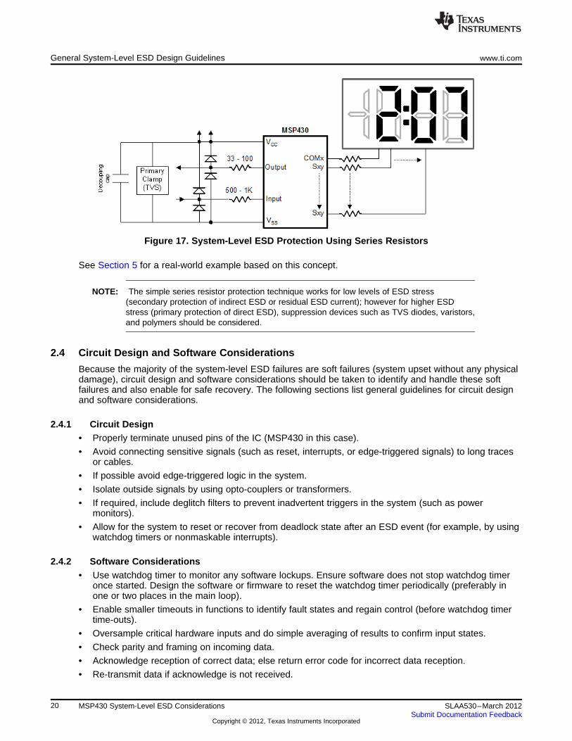
Consider a system where an MSP430 IC is interfaced to an LCD that is susceptible to ESD (secondary orresidual ESD stress in the system). In this case, LCD pins represent the ESD entry points in the system;so, it is recommended to place series resistors on the LCD pins. When an ESD event occurs in thesystem, the series resistor limits the current that finally strikes the MSP430 I/O pin. The larger the value ofresistance, the lower is the residual current seen at the interface I/O pin.
NOTE: If standalone resistors are used for primary ESD protection, they must withstand the fullelectrostatic voltage. This requires resistors that are designed for high voltages, and theseusually have a larger footprint.
The series resistors can be combined with additional diodes and primary clamping devices for addedprotection (see the equivalent circuit shown in Figure 17). The diodes at the I/O pins divert the ESDcurrent to the primary clamp (between VCC and VSS), and only the residual stress appears at the deviceI/O pins. The decoupling capacitor at the supply pins helps limit the initial fast transients of the ESD pulse.
19SLAA530–March 2012 MSP430 System-Level ESD ConsiderationsSubmit Documentation Feedback
Copyright © 2012, Texas Instruments Incorporated
General System-Level ESD Design Guidelines www.ti.com
Figure 17. System-Level ESD Protection Using Series Resistors
See Section 5 for a real-world example based on this concept.
NOTE: The simple series resistor protection technique works for low levels of ESD stress(secondary protection of indirect ESD or residual ESD current); however for higher ESDstress (primary protection of direct ESD), suppression devices such as TVS diodes, varistors,and polymers should be considered.
2.4 Circuit Design and Software Considerations
Because the majority of the system-level ESD failures are soft failures (system upset without any physicaldamage), circuit design and software considerations should be taken to identify and handle these softfailures and also enable for safe recovery. The following sections list general guidelines for circuit designand software considerations.
2.4.1 Circuit Design• Properly terminate unused pins of the IC (MSP430 in this case).
• Avoid connecting sensitive signals (such as reset, interrupts, or edge-triggered signals) to long tracesor cables.
• If possible avoid edge-triggered logic in the system.
• Isolate outside signals by using opto-couplers or transformers.
• If required, include deglitch filters to prevent inadvertent triggers in the system (such as powermonitors).
• Allow for the system to reset or recover from deadlock state after an ESD event (for example, by usingwatchdog timers or nonmaskable interrupts).
2.4.2 Software Considerations• Use watchdog timer to monitor any software lockups. Ensure software does not stop watchdog timer
once started. Design the software or firmware to reset the watchdog timer periodically (preferably inone or two places in the main loop).
• Enable smaller timeouts in functions to identify fault states and regain control (before watchdog timertime-outs).
• Oversample critical hardware inputs and do simple averaging of results to confirm input states.
• Check parity and framing on incoming data.
• Acknowledge reception of correct data; else return error code for incorrect data reception.
• Re-transmit data if acknowledge is not received.
20 MSP430 System-Level ESD Considerations SLAA530–March 2012Submit Documentation Feedback
Copyright © 2012, Texas Instruments Incorporated
www.ti.com General System-Level ESD Design Guidelines
2.5 ESD Testing
ESD testing throughout design and development helps identify and fix weak ESD spots in the system. On-board LEDs and switches can be used to debug different ESD failure categories. Listed below are thedifferent system-level ESD failure criteria as per IEC 61000-4-2 [1] and example failure conditions whenusing an MSP430 device in the system:
1. Normal performance within specification limits
• MSP430 is not affected by the system-level ESD stress and continues to execute without anyintervention.
2. Temporary degradation or loss of function or performance which is self-recoverable
• Device reset can occur (for example, caused by low pulse on the MSP430 reset pin that causesthe device to reset).
• Oscillator disturbance can occur (for example, caused by on-board crystal dropping out). Thiscondition can be identified by on-chip watchdog or oscillator fault detection.
NOTE: In this case, the on-board LEDs and the reset interrupt vector (that helps identify the lastcause of a reset – BOR, POR, or PUC) can be used to the identify the failure andrecovery conditions
3. Temporary degradation or loss of function or performance that requires operator intervention or systemreset
• Device upset that requires user to manually apply a low pulse on the reset pin or a power-cycle.
NOTE: In this case, on-board switches can be used on the test board to recover the device
4. Degradation or loss of function that is not recoverable due to damage of equipment (components) orsoftware, or loss of data
• Damage of MSP430 I/O pin structure. This might result in system upsets such as non-operationalinterrupts associated with the I/O pins.
• Increased leakage current caused by degradation or damage of integrated components andcircuits connected to I/O pins or power supply pins.
• Loss of CODE or DATA on device RAM or non-volatile memory.
• Device enters deadlock state by poorly designed software.
See IEC standards [1] for the standard system-level ESD tests, thresholds, and ratings.
21SLAA530–March 2012 MSP430 System-Level ESD ConsiderationsSubmit Documentation Feedback
Copyright © 2012, Texas Instruments Incorporated
System Efficient ESD Design (SEED) www.ti.com
3 System Efficient ESD Design (SEED)
System Efficient ESD Design or SEED is a new co-design approach that is introduced in the JEP161JEDEC publication [2] to limit the damaging current pulses reaching the internal IC pins. It helps tounderstand the physical effect of an IEC stress applied at the external port of a PCB on the IC pin.
3.1 System-Level ESD Protection Methodology
SEED is a co-design methodology of on-board and on-chip ESD protection that helps analyze andachieve system-level ESD robustness. This design approach requires thorough understanding of theinteractions between external ESD pulses, full system level board design and device pin characteristicsduring an ESD stress event.
3.1.1 On-Board Protection – Primary Clamp
The on-board protection in the system represents the primary system-level ESD protection (also known asthe primary clamp) and, as discussed in Section 2, the system-level ESD protection at the PCB levelstrongly depends on the physical design of the product and its operational requirements. With a good end-product enclosure or cover design, the on-board protection can focus on external connections as well asany cover hole or seam areas that may leak ESD energy inside. The on-board protection circuitry mightinclude clamping components like Transient Voltage Suppression (TVS) diodes, varistors, polymers, andso on.
These primary clamps can shunt large stress currents at low capacitive loads and are effective in reducingthe residual ESD stress that eventually appears at the device pins. By characterizing the PCB, asufficiently detailed RLC network model can be extracted, which allows for simulation of the board thatincludes the passive components and the ESD voltage clamping elements under system-level ESD stress.This PCB characterization information is system- and board-specific and is critical for the SEED designanalysis.
3.1.2 On-Chip Protection – Secondary Clamp
The on-chip protection of an IC pin in the system represents the secondary system-level ESD protection(also known as the secondary clamp), which is used to clamp the residual ESD stress that results at thespecific device pins after having passed the primary clamp in the system. Because the shape and energyof the residual ESD pulse is largely dependent on the on-board primary clamp characteristics and theboard itself, it is generally unknown. This clearly implies that the on-chip ESD protection alone is notsufficient to overall ensure specified system-level robustness.
The effectiveness of the secondary clamp must be analyzed with respect to the system-specific PCBcharacterization data and the IC-level I/O characterization data such as Transmission Line Pulse (TLP)parameters to determine if the peak residual ESD voltage and current seen at the specific device pins inthe system are within the scope of the on-chip ESD protection capabilities.
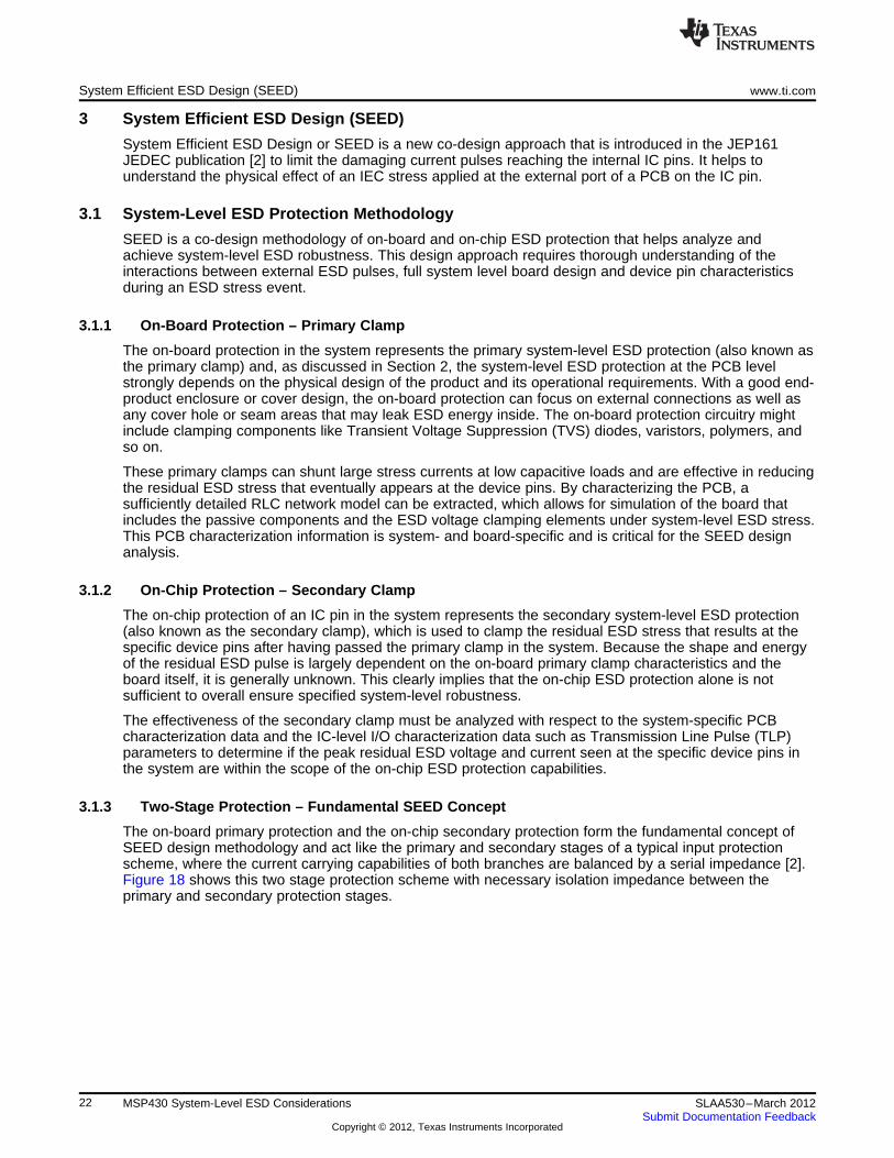
3.1.3 Two-Stage Protection – Fundamental SEED Concept
The on-board primary protection and the on-chip secondary protection form the fundamental concept ofSEED design methodology and act like the primary and secondary stages of a typical input protectionscheme, where the current carrying capabilities of both branches are balanced by a serial impedance [2].Figure 18 shows this two stage protection scheme with necessary isolation impedance between theprimary and secondary protection stages.
22 MSP430 System-Level ESD Considerations SLAA530–March 2012Submit Documentation Feedback
Copyright © 2012, Texas Instruments Incorporated
www.ti.com System Efficient ESD Design (SEED)
NOTE: Matched primary (on-board TVS) and secondary (IC ESD protection) clamps
Figure 18. Two-Stage System-Level ESD Protection [7]
Simulating and analyzing the two-stage protection using the SEED methodology enables board designersto select appropriate on-board protection for primary clamping and other board components (isolationimpedance) to ensure peak residual pulse reaching the IC pins (with on-chip ESD protection) can still behandled effectively in preventing any physical device damage and other system level upsets. Moreinformation regarding the SEED co-design methodology can be found in the JPEP161 System-level ESDdocument [2].
In summary, this new co-design methodology concept demonstrates that (1) high-level component-levelprotection (HBM) does not necessarily ensure effective system ESD robustness, and (2) understandingthe interactions between external ESD stress and full system-level design (including ICs in the system)enables achievement of robust system ESD designs with on-chip HBM levels reduced to a more realisticvalue accepted for IC handling.
3.2 SPICE Simulation Methodology for System-Level ESD Design
This section discusses the SPICE simulation methodology to design an isolation impedance networkagainst the residual pulse from an IEC 61000-4-2 stress using the Transmission Line Protection (TLP)data of on-board TVS components (primary clamp) and the IC interface pins (secondary clamp). Thesimulation procedure follows these steps:
1. Model the IEC stress waveform
The IEC stress waveform can be modeled by using simple RLC circuits. Figure 20 in Section 4.1shows an IEC model circuit and the corresponding IEC stress waveform generated. The values of R, L,and C for both branches have to be tweaked to suitably represent the standard IEC stress waveformand are partly based on the well known 330-Ω and 150-pF model [8].
2. Model the TLP behavior of the TVS device
The on-board TVS device (used as a primary clamp in the system) can be modeled for SPICEsimulation based on device TLP information, which includes the worst-case breakdown voltage(referred to as VTVS,t1,max) and the dynamic on-resistance (referred to as RTVS,on,max). The TVS device ismodeled by a Zener diode. The VTVS,t1,max defines the breakdown voltage of the zener diode, and the
23SLAA530–March 2012 MSP430 System-Level ESD ConsiderationsSubmit Documentation Feedback
Copyright © 2012, Texas Instruments Incorporated
System Efficient ESD Design (SEED) www.ti.com
RTVS,on,max defines the value of the fitted series resistor. See Appendix A for more details.
NOTE: The TVS device manufacturer should ideally provide the TLP parameters required for SEEDmethodology in the device datasheet. If wanting to use a TVS device that does not have thenecessary TLP parameters made available, then the board designer or OEM has tocharacterize and model the TVS on their end.
3. Behavior of the interface pin to be protected
A modeling approach similar to that of the TVS device can be used to model the IC interface pin to beprotected. The SEED parameters required to model the I/O pin's on-chip ESD protection are derivedfrom TLP measurements and should be provided by the component manufacturer. Using SPICEsimulation, the IC pin is represented as a zener diode with a fitted series resistor. The following IC pinESD protection specifications are used for modeling: (a) minimum turn-on voltage once ESD protectionis triggered (referred to as VIC,t1,min), (b) maximum acceptable current (referred to as IIC,max), and (c)minimum dynamic on-resistance (referred to as RIC,on,min). See Appendix A for more details.
NOTE: As of this writing, Texas Instruments does not characterize or specify SEED parameters forany MSP430 product as a part of the device data sheets. As a member of the IndustryCouncil on ESD Target Levels, Texas Instruments is working on the specification of theparameters needed to support the SEED methodology.
4. Calibrate with measured test board data
This step includes calibrating the SPICE simulation model based on the test board data. It shouldaccommodate for multi-stage on-board primary clamping (multiple TVS devices) and any additionalisolation impedance between the IEC stress point in the system and the IC interface pin.
5. IEC Protection design using SPICE simulation
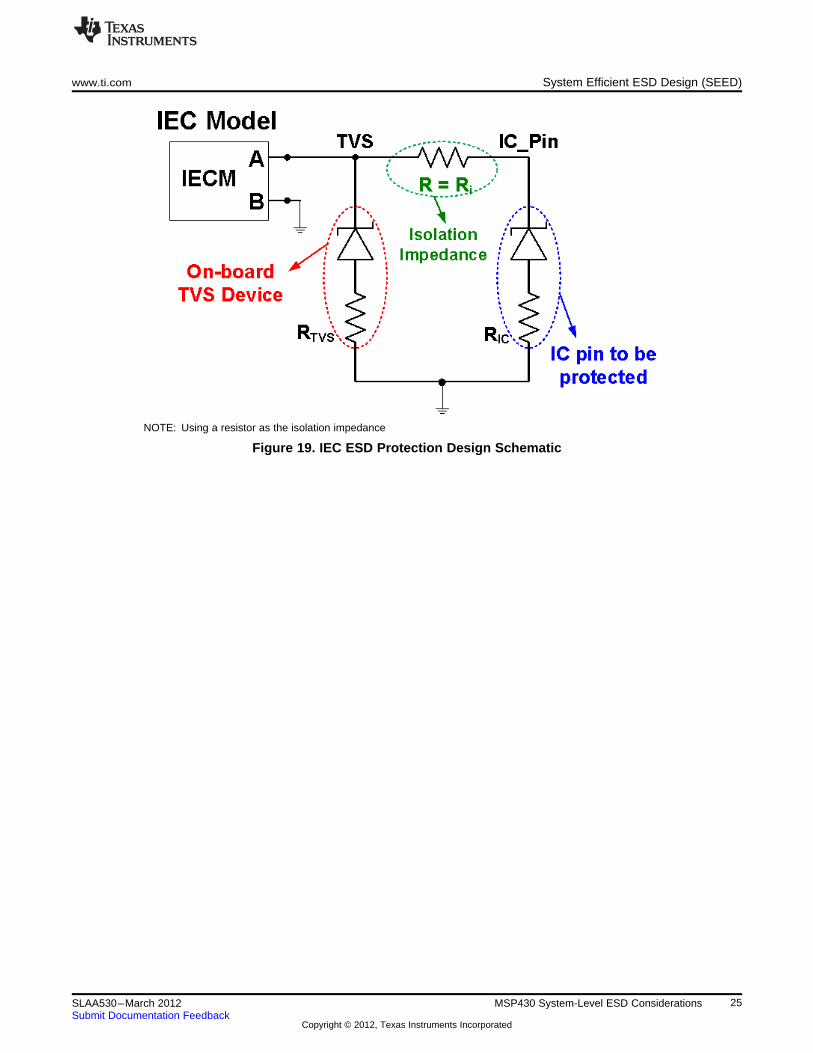
The IEC protection design using SPICE simulation involves putting together the IEC stress model, TVSand IC interface pin models based on respective SEED parameters and an isolation impedancecircuitry. Figure 19 shows an example SPICE simulation of an IEC protection design with a resistorused as the isolation impedance between the primary and secondary clamps.
NOTE: A decoupling capacitor can be connected in parallel to the primary clamp to (1) limit thevoltage of the initial fast transient ESD current pulse at the TVS node and (2) limit thevoltage slew rate (that is, dV/dt) of this fast transient. Because the response of IC pins toESD events does not depend on the quasi-static characteristics of the given stress alone butalso on its transient characteristics, this decoupling capacitor becomes essential in mostsystem-level ESD designs.
24 MSP430 System-Level ESD Considerations SLAA530–March 2012Submit Documentation Feedback
Copyright © 2012, Texas Instruments Incorporated
www.ti.com System Efficient ESD Design (SEED)
NOTE: Using a resistor as the isolation impedance
Figure 19. IEC ESD Protection Design Schematic
25SLAA530–March 2012 MSP430 System-Level ESD ConsiderationsSubmit Documentation Feedback
Copyright © 2012, Texas Instruments Incorporated
SEED-Based IEC Protection Design and Verification – Real World Example 1 www.ti.com
4 SEED-Based IEC Protection Design and Verification – Real World Example 1
This section shows a real world example of system level IEC protection design and verification that uses astandard TVS device as a primary clamp and a specific MSP430 device interface pin with the on-chip ESDprotection as the secondary clamp. The SEED methodology has been applied using SPICE simulations todetermine the isolation impedance required in the system to ensure that the peak ESD current and voltagereaching the MSP430 interface pin is within the on-chip protection capabilities. Finally, this analysis hasbeen verified by system-level ESD testing using verification test boards.
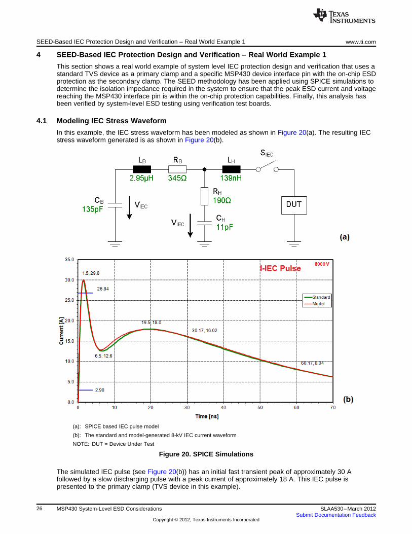
4.1 Modeling IEC Stress Waveform
In this example, the IEC stress waveform has been modeled as shown in Figure 20(a). The resulting IECstress waveform generated is as shown in Figure 20(b).
(a): SPICE based IEC pulse model
(b): The standard and model-generated 8-kV IEC current waveform
NOTE: DUT = Device Under Test
Figure 20. SPICE Simulations
The simulated IEC pulse (see Figure 20(b)) has an initial fast transient peak of approximately 30 Afollowed by a slow discharging pulse with a peak current of approximately 18 A. This IEC pulse ispresented to the primary clamp (TVS device in this example).
26 MSP430 System-Level ESD Considerations SLAA530–March 2012Submit Documentation Feedback
Copyright © 2012, Texas Instruments Incorporated
www.ti.com SEED-Based IEC Protection Design and Verification – Real World Example 1
4.2 Modeling TVS Device
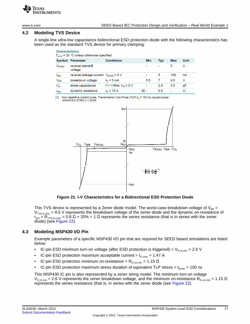
A single-line ultra-low capacitance bidirectional ESD protection diode with the following characteristics hasbeen used as the standard TVS device for primary clamping:
Figure 21. I-V Characteristics for a Bidirectional ESD Protection Diode
This TVS device is represented by a Zener diode model. The worst-case breakdown voltage of VBR =VTVS,t1,max = 9.5 V represents the breakdown voltage of the zener diode and the dynamic on-resistance ofrdyn = RTVS,on,max = 0.8 Ω + 20% = 1 Ω represents the series resistance (that is in series with the zenerdiode) (see Figure 22).
4.3 Modeling MSP430 I/O Pin
Example parameters of a specific MSP430 I/O pin that are required for SEED based simulations are listedbelow:
• IC-pin ESD minimum turn-on voltage (after ESD protection is triggered) = VIC,t1,min = 2.6 V
• IC-pin ESD protection maximum acceptable current = IIC,max = 1.47 A
• IC-pin ESD protection minimum on-resistance = RIC,on,min = 1.15 Ω• IC-pin ESD protection maximum stress duration of equivalent TLP stress = tDmax = 100 ns
This MSP430 IC pin is also represented by a zener string model. The minimum turn-on voltageVIC,t1,min = 2.6 V represents the zener breakdown voltage, and the minimum on-resistance RIC,on,min = 1.15 Ωrepresents the series resistance (that is, in series with the zener diode (see Figure 22).
27SLAA530–March 2012 MSP430 System-Level ESD ConsiderationsSubmit Documentation Feedback
Copyright © 2012, Texas Instruments Incorporated
TVS,max IC,maxi,min
IC,max
i,min
i,min
V – VR =
I
27.5 V – 4.3 VR =
1.47 A
R 16» W
SEED-Based IEC Protection Design and Verification – Real World Example 1 www.ti.com
4.4 Isolated Impedance Calculation
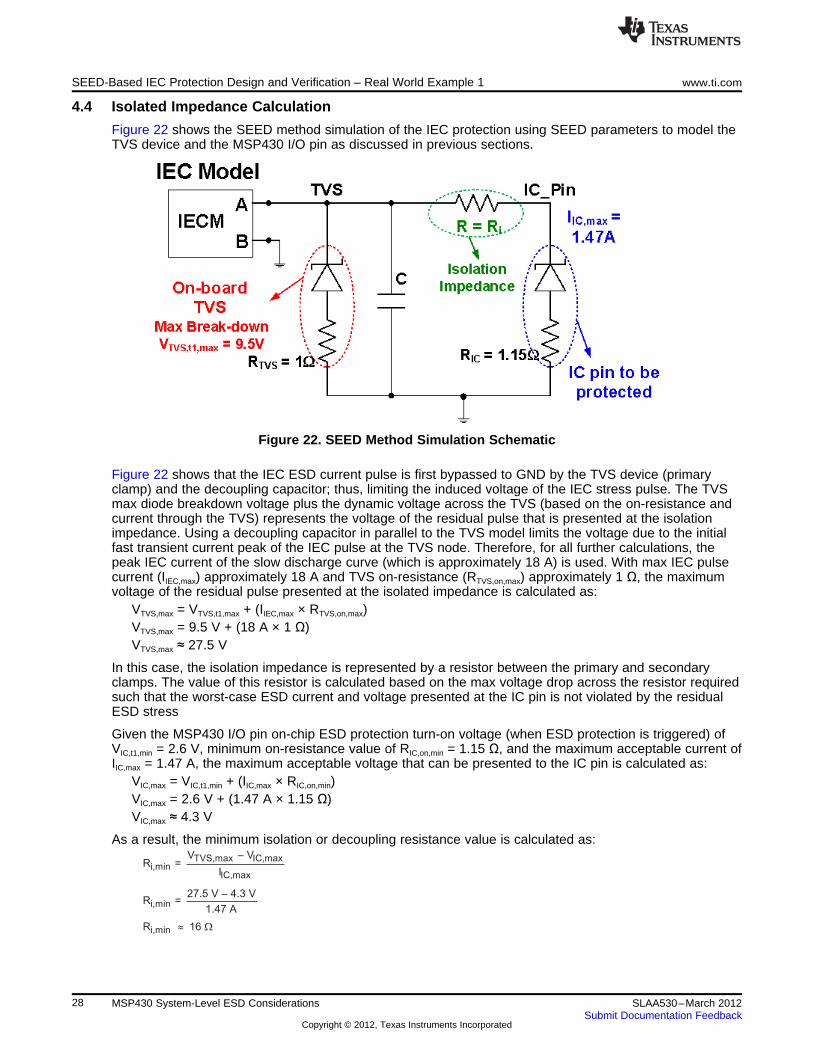
Figure 22 shows the SEED method simulation of the IEC protection using SEED parameters to model theTVS device and the MSP430 I/O pin as discussed in previous sections.
Figure 22. SEED Method Simulation Schematic
Figure 22 shows that the IEC ESD current pulse is first bypassed to GND by the TVS device (primaryclamp) and the decoupling capacitor; thus, limiting the induced voltage of the IEC stress pulse. The TVSmax diode breakdown voltage plus the dynamic voltage across the TVS (based on the on-resistance andcurrent through the TVS) represents the voltage of the residual pulse that is presented at the isolationimpedance. Using a decoupling capacitor in parallel to the TVS model limits the voltage due to the initialfast transient current peak of the IEC pulse at the TVS node. Therefore, for all further calculations, thepeak IEC current of the slow discharge curve (which is approximately 18 A) is used. With max IEC pulsecurrent (IIEC,max) approximately 18 A and TVS on-resistance (RTVS,on,max) approximately 1 Ω, the maximumvoltage of the residual pulse presented at the isolated impedance is calculated as:
VTVS,max = VTVS,t1,max + (IIEC,max × RTVS,on,max)VTVS,max = 9.5 V + (18 A × 1 Ω)VTVS,max ≈ 27.5 V
In this case, the isolation impedance is represented by a resistor between the primary and secondaryclamps. The value of this resistor is calculated based on the max voltage drop across the resistor requiredsuch that the worst-case ESD current and voltage presented at the IC pin is not violated by the residualESD stress
Given the MSP430 I/O pin on-chip ESD protection turn-on voltage (when ESD protection is triggered) ofVIC,t1,min = 2.6 V, minimum on-resistance value of RIC,on,min = 1.15 Ω, and the maximum acceptable current ofIIC,max = 1.47 A, the maximum acceptable voltage that can be presented to the IC pin is calculated as:
VIC,max = VIC,t1,min + (IIC,max × RIC,on,min)VIC,max = 2.6 V + (1.47 A × 1.15 Ω)VIC,max ≈ 4.3 V
As a result, the minimum isolation or decoupling resistance value is calculated as:
28 MSP430 System-Level ESD Considerations SLAA530–March 2012Submit Documentation Feedback
Copyright © 2012, Texas Instruments Incorporated
www.ti.com SEED-Based IEC Protection Design and Verification – Real World Example 1
4.5 SPICE Simulation – SEED Method
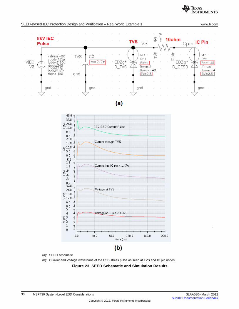
Figure 23(a) shows the SPICE simulation schematic of the IEC Protection design using the SEEDmethodology. It consists of the following blocks:
• IEC ESD pulse generator as shown in Figure 20. An 8-kV IEC pulse with initial transient peak ofapproximately 30 A and slow discharge curve with peak current of approximately 18 A is generated.
• TVS diode model with maximum breakdown voltage of 9.5 V and dynamic on-resistance of 1 Ω.
• Minimum decoupling capacitor with a capacitance value of 2.2 nF (in parallel to the TVS model) usedto limit the voltage induced by the initial fast transient current spike.
• Decoupling resistor of 16 Ω between the TVS device and device interface pin models.
• MSP430 device interface pin model with minimum turn-on voltage of 2.6 V and minimum on-resistanceof 1.15 Ω.
The SPICE simulation waveforms (both the current and voltage curves) at the TVS and IC pin nodes areas shown in Figure 23(b). Simulation waveforms show the peak current and voltage values of IIEC,max
approximately 18 A and VTVS,max approximately 26.5 V at the TVS node respectively, and less than IIC,max of1.47 A and VIC,max of 4.3 V at the IC pin node respectively. These results match nicely with the results ofthe calculation in Section 4.4.
29SLAA530–March 2012 MSP430 System-Level ESD ConsiderationsSubmit Documentation Feedback
Copyright © 2012, Texas Instruments Incorporated
SEED-Based IEC Protection Design and Verification – Real World Example 1 www.ti.com
(a): SEED schematic
(b): Current and Voltage waveforms of the ESD stress pulse as seen at TVS and IC pin nodes
Figure 23. SEED Schematic and Simulation Results
30 MSP430 System-Level ESD Considerations SLAA530–March 2012Submit Documentation Feedback
Copyright © 2012, Texas Instruments Incorporated
www.ti.com SEED-Based IEC Protection Design and Verification – Real World Example 1
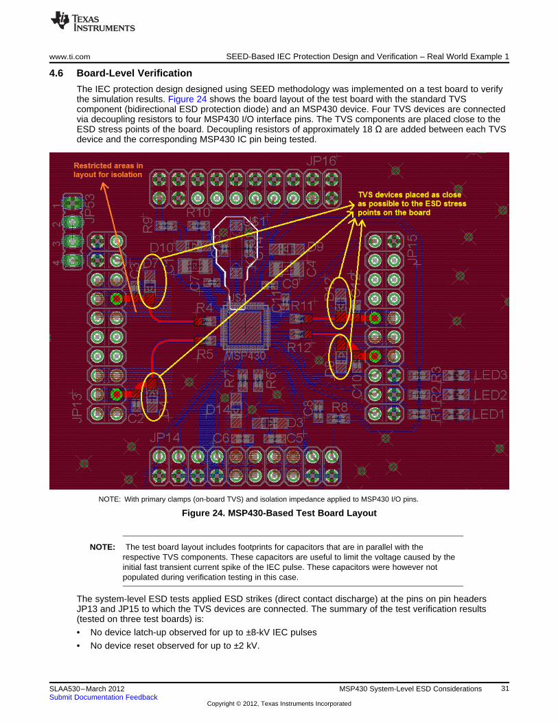
4.6 Board-Level Verification
The IEC protection design designed using SEED methodology was implemented on a test board to verifythe simulation results. Figure 24 shows the board layout of the test board with the standard TVScomponent (bidirectional ESD protection diode) and an MSP430 device. Four TVS devices are connectedvia decoupling resistors to four MSP430 I/O interface pins. The TVS components are placed close to theESD stress points of the board. Decoupling resistors of approximately 18 Ω are added between each TVSdevice and the corresponding MSP430 IC pin being tested.
NOTE: With primary clamps (on-board TVS) and isolation impedance applied to MSP430 I/O pins.
Figure 24. MSP430-Based Test Board Layout
NOTE: The test board layout includes footprints for capacitors that are in parallel with therespective TVS components. These capacitors are useful to limit the voltage caused by theinitial fast transient current spike of the IEC pulse. These capacitors were however notpopulated during verification testing in this case.
The system-level ESD tests applied ESD strikes (direct contact discharge) at the pins on pin headersJP13 and JP15 to which the TVS devices are connected. The summary of the test verification results(tested on three test boards) is:
• No device latch-up observed for up to ±8-kV IEC pulses
• No device reset observed for up to ±2 kV.
31SLAA530–March 2012 MSP430 System-Level ESD ConsiderationsSubmit Documentation Feedback
Copyright © 2012, Texas Instruments Incorporated
System-Level ESD Protection – Real World Example 2 www.ti.com
5 System-Level ESD Protection – Real World Example 2
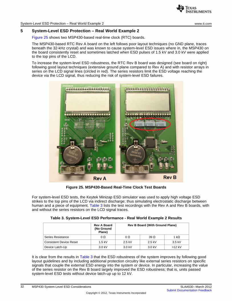
Figure 25 shows two MSP430-based real-time clock (RTC) boards.
The MSP430-based RTC Rev A board on the left follows poor layout techniques (no GND plane, tracesbeneath the 32-kHz crystal) and was known to cause system-level ESD issues where in, the MSP430 onthe board consistently reset and sometimes latched when ESD pulses of 1.5 kV and 3.0 kV were appliedto the top pins of the LCD.
To increase the system-level ESD robustness, the RTC Rev B board was designed (see board on right)following good layout techniques (extensive ground plane compared to Rev A) and with resistor arrays inseries on the LCD signal lines (circled in red). The series resistors limit the ESD voltage reaching thedevice via the LCD signal, thus reducing the risk of system-level ESD failures.
Figure 25. MSP430-Based Real-Time Clock Test Boards
For system-level ESD tests, the Keytek Minizap ESD simulator was used to apply high voltage ESDstrikes to the top pins of the LCD via indirect discharge; thus simulating electrostatic discharge betweenhuman and a piece of equipment. Table 3 lists the test recordings with the Rev A and Rev B boards, withand without the series resistors on the LCD signal traces.
Table 3. System-Level ESD Performance - Real World Example 2 Results
Rev A Board Rev B Board (With Ground Plane)(No Ground
Plane)
Series Resistance 0 Ω 0 Ω 39 Ω 1 kΩConsistent Device Reset 1.5 kV 2.5 kV 2.5 kV 3.5 kV
Device Latch-Up 3.0 kV 3.0 kV 3.0 kV >12 kV
It is clear from the results in Table 3 that the ESD robustness of the system improves by following goodlayout guidelines and by including additional protection circuitry like external series resistors on specificsignals that couple the external ESD energy into the system or device. In particular, increasing the valueof the series resistor on the Rev B board largely improved the ESD robustness; that is, units passedsystem-level ESD tests without device latch-up up to 12 kV.
32 MSP430 System-Level ESD Considerations SLAA530–March 2012Submit Documentation Feedback
Copyright © 2012, Texas Instruments Incorporated
www.ti.com Summary
NOTE: A crystal clock failure was reported on Rev A board due to the poor layout techniques. Onthe Rev A board, it can be noticed that the digital signal traces are running underneath the32-kHz crystal on the PCB. Toggling these digital signals cause the crystal clock generatedby the MSP430 on-chip oscillator to fail. This failure was not seen on the Rev B due to goodlayout techniques (that is, no traces underneath the crystal layout). For more informationregarding crystal layout considerations, see the application report MSP430 32-kHz CrystalOscillator [11].
6 Summary
Component-level ESD ratings (HBM and CDM) do not correlate with system-level ESD ratings (IEC). Thecomponent-level ratings address component or IC handling in ESD-protected areas (EPA) such asmanufacturing and assembly environments. Increasing the component-level ESD rating to protect thedevice against system-level ESD pulses leads to increased IC area and reduced functional performance(for example, increased leakage current or reduced switching speed) and can be uneconomical, especiallywhen compared to adding external on-board ESD protection for system-level ESD protection. And, in mostof the cases, even with increased IC-level ESD rating, complete system level ESD robustness is still notachieved. On the contrary, with improvements in manufacturing ESD controls, the Industry Council forESD Target Levels and JEDEC has recommended lowering the component-level ESD ratings that arerequired for a safe handling of ICs.
Designing an ESD robust system needs a holistic approach. It requires the board designers and OEMs to(1) understand and evaluate ESD effects in their system early in design; (2) follow ESD-immune designguidelines in the design and development from the beginning; and (3) perform system-level ESD testing(per IEC 61000-4-2) at various development stages to help identify and fix ESD-related weaknesses in thedesign.
33SLAA530–March 2012 MSP430 System-Level ESD ConsiderationsSubmit Documentation Feedback
Copyright © 2012, Texas Instruments Incorporated
References www.ti.com
7 References1. International Electrotechnical Commission, IEC 61000-4-2, Electromagnetic capability (EMC) – Part 4-
2: Testing and measurement techniques – Electrostatic discharge immunity test, Ed. 2.0
2. JEDEC Publication (White Paper 3) JEP161: System-level ESD Part I: Common Misconceptions andRecommended Basic Approaches
3. ESDA/JEDEC Joint Standard for Electrostatic Discharge Sensitivity Testing – Human Body Model–Component Level, ANSI ESDA/JEDEC JS-001-2011
4. JESD22-C101 Field-Induced Charged-Device Model Test Method for Electrostatic DischargeWithstand Thresholds of Microelectronic Components
5. Texas Instruments Inc., ESD and EMI Device Protection Product Portfolio, www.ti.com/emi
6. ISO Standard 10605 Road vehicles – Test methods for electrical disturbances from electrostaticdischarge, International Organization for Standardization, 2008
7. S. Marum, C. Duvvury, J. Park, A. Chadwick, A. Jahanzeb; Protection Circuits from the TransientVoltage Suppressor's Residual Pulse During IEC 61000-4-2 Stress, Proc. EOS/ESD Symposium 2009(2009)
8. Lifang Lou, Charvaka Duvvury, Agha Jahanzeb, Jae Park; SPICE Simulation Methodology for System-level ESD Design, Proc EOS/ESD Symposium 2010 (2010)
9. Industry Council on ESD Target Levels, White Paper 1: A Case for Lowering Component LevelHBM/MM ESD Specifications and Requirements, August 2007, at www.esda.org or JEDEC publicationJEP155, Recommended ESD Target Levels for HBM/MM Qualification, www.jedec.org
10. Industry Council on ESD Target Levels, White Paper 2: A Case for Lowering Component Level CDMESD Specifications and Requirements, Revision 2, April 2010, at www.esda.org or JEDEC publicationJEP157, ‘Recommended ESD-CDM Target Levels', www.jedec.org
11. MSP430 32-kHz Crystal Oscillator (SLAA322)
12. High-Speed Layout Guidelines (SCAA082)
13. ESD Association Standard for the development of an Electrostatic Discharge Control Program forProtection of Electrical and Electronic Parts, Assemblies and Equipment (Excluding Electrically InitiatedExplosive Devices), ANSI/ESD S20.20-2007
14. International Electrotechnical Commission, IEC 61340 standards family, Electrostatics - Part 2-1 to 5-3
15. Industry Council on ESD Target Levels, http://www.esdindustrycouncil.org
34 MSP430 System-Level ESD Considerations SLAA530–March 2012Submit Documentation Feedback
Copyright © 2012, Texas Instruments Incorporated
www.ti.com
Appendix A Modeling Using TLP Parameters
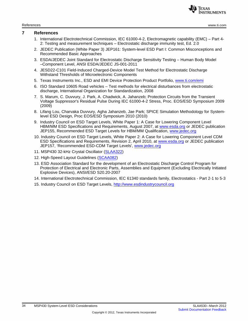
A.1 Modeling TVS Device Using TLP Parameters [8]
This example case discusses the modeling of a TVS device that acts as a Zener diode, turning on atapproximately 7 V. Its 100-ns TLP I-V characteristic is shown in Figure 26(a). The SPICE model isgenerated based on I-V data using a zener diode model, as shown in Figure 26(b). The trigger voltage isrepresented by the zener breakdown voltage and the on-resistance by a fitted series resistor. Thesimulation in Figure 26(b) is tuned to match the quasi-static TLP characteristic in Figure 26(a) asconfirmed by the DC sweep in Figure 26(c).
(a): Quasi-static 100-ns TLP I-V curve
(b): The respective SPICE model
(c): The simulation results of the TVS [8]
Figure 26. Modeling TVS Device Using TLP Parameters
35SLAA530–March 2012 MSP430 System-Level ESD ConsiderationsSubmit Documentation Feedback
Copyright © 2012, Texas Instruments Incorporated
Modeling IC Interface Pin to be Protected Using TLP Parameters [8] www.ti.com
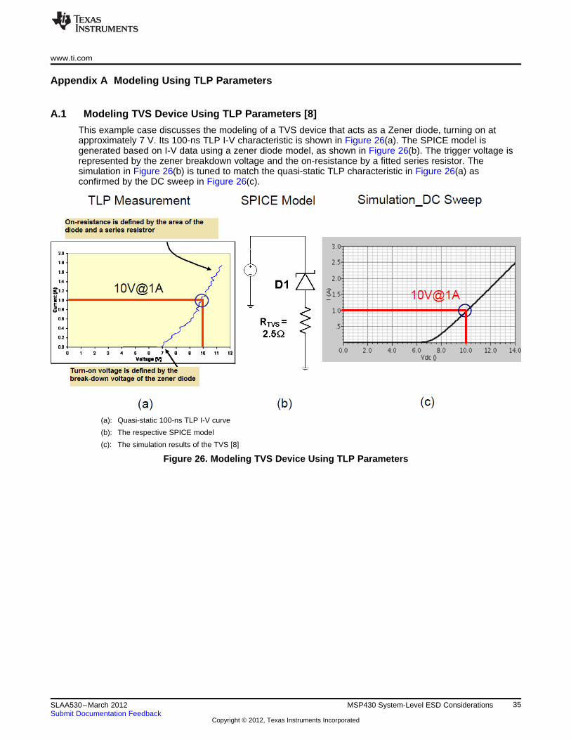
A.2 Modeling IC Interface Pin to be Protected Using TLP Parameters [8]
This example case discusses the modeling of an IC interface pin with the 100-ns TLP I-V characteristic asshown in Figure 27(a). The SPICE model is generated based on the quasi-static I-V characteristic using azener diode, as shown in Figure 27(b).
(a): Quasi-static 100-ns TLP I-V curve
(b): The respective SPICE model
(c): The simulation results of an example IC interface pin [8]
Figure 27. Modeling IC Interface Pin Using TLP Parameters
NOTE: The TLP data used in this example is not related to MSP430 devices and are used only toshow the modeling process.
FromFigure 27(a) and Figure 27(c), it can be seen that the actual turn-on point as per the TLP I-V curveand the TLP model simulation is at 2.6 V and 3.4 V, respectively. However, the model simulation matchesthe TLP data in the conduction region which is more relevant. Therefore, when tweaking the clampingdevice model to match the TLP data, the conduction region is more important than the turn-on point if acompromise must be made.
36 MSP430 System-Level ESD Considerations SLAA530–March 2012Submit Documentation Feedback
Copyright © 2012, Texas Instruments Incorporated
IMPORTANT NOTICE
Texas Instruments Incorporated and its subsidiaries (TI) reserve the right to make corrections, modifications, enhancements, improvements,and other changes to its products and services at any time and to discontinue any product or service without notice. Customers shouldobtain the latest relevant information before placing orders and should verify that such information is current and complete. All products aresold subject to TI’s terms and conditions of sale supplied at the time of order acknowledgment.
TI warrants performance of its hardware products to the specifications applicable at the time of sale in accordance with TI’s standardwarranty. Testing and other quality control techniques are used to the extent TI deems necessary to support this warranty. Except wheremandated by government requirements, testing of all parameters of each product is not necessarily performed.
TI assumes no liability for applications assistance or customer product design. Customers are responsible for their products andapplications using TI components. To minimize the risks associated with customer products and applications, customers should provideadequate design and operating safeguards.
TI does not warrant or represent that any license, either express or implied, is granted under any TI patent right, copyright, mask work right,or other TI intellectual property right relating to any combination, machine, or process in which TI products or services are used. Informationpublished by TI regarding third-party products or services does not constitute a license from TI to use such products or services or awarranty or endorsement thereof. Use of such information may require a license from a third party under the patents or other intellectualproperty of the third party, or a license from TI under the patents or other intellectual property of TI.
Reproduction of TI information in TI data books or data sheets is permissible only if reproduction is without alteration and is accompaniedby all associated warranties, conditions, limitations, and notices. Reproduction of this information with alteration is an unfair and deceptivebusiness practice. TI is not responsible or liable for such altered documentation. Information of third parties may be subject to additionalrestrictions.
Resale of TI products or services with statements different from or beyond the parameters stated by TI for that product or service voids allexpress and any implied warranties for the associated TI product or service and is an unfair and deceptive business practice. TI is notresponsible or liable for any such statements.
TI products are not authorized for use in safety-critical applications (such as life support) where a failure of the TI product would reasonablybe expected to cause severe personal injury or death, unless officers of the parties have executed an agreement specifically governingsuch use. Buyers represent that they have all necessary expertise in the safety and regulatory ramifications of their applications, andacknowledge and agree that they are solely responsible for all legal, regulatory and safety-related requirements concerning their productsand any use of TI products in such safety-critical applications, notwithstanding any applications-related information or support that may beprovided by TI. Further, Buyers must fully indemnify TI and its representatives against any damages arising out of the use of TI products insuch safety-critical applications.
TI products are neither designed nor intended for use in military/aerospace applications or environments unless the TI products arespecifically designated by TI as military-grade or "enhanced plastic." Only products designated by TI as military-grade meet militaryspecifications. Buyers acknowledge and agree that any such use of TI products which TI has not designated as military-grade is solely atthe Buyer's risk, and that they are solely responsible for compliance with all legal and regulatory requirements in connection with such use.
TI products are neither designed nor intended for use in automotive applications or environments unless the specific TI products aredesignated by TI as compliant with ISO/TS 16949 requirements. Buyers acknowledge and agree that, if they use any non-designatedproducts in automotive applications, TI will not be responsible for any failure to meet such requirements.
Following are URLs where you can obtain information on other Texas Instruments products and application solutions:
Products Applications
Audio www.ti.com/audio Automotive and Transportation www.ti.com/automotive
Amplifiers amplifier.ti.com Communications and Telecom www.ti.com/communications
Data Converters dataconverter.ti.com Computers and Peripherals www.ti.com/computers
DLP® Products www.dlp.com Consumer Electronics www.ti.com/consumer-apps
DSP dsp.ti.com Energy and Lighting www.ti.com/energy
Clocks and Timers www.ti.com/clocks Industrial www.ti.com/industrial
Interface interface.ti.com Medical www.ti.com/medical
Logic logic.ti.com Security www.ti.com/security
Power Mgmt power.ti.com Space, Avionics and Defense www.ti.com/space-avionics-defense
Microcontrollers microcontroller.ti.com Video and Imaging www.ti.com/video
RFID www.ti-rfid.com
OMAP Mobile Processors www.ti.com/omap
Wireless Connectivity www.ti.com/wirelessconnectivity
TI E2E Community Home Page e2e.ti.com
Mailing Address: Texas Instruments, Post Office Box 655303, Dallas, Texas 75265Copyright © 2012, Texas Instruments Incorporated