Embed Size (px)
Citation preview
ESP-WROOM-32 Datasheet
Espressif Systems
August 22, 2016
About This Guide
This document lists the specifications for the ESP-WROOM-32 module.
The document structure is as follows:
Chapter Title Subject
Chapter 1 Preface A preview of ESP-WROOM-32
Chapter 2 Pin Definitions Device pinout and pin descriptions
Chapter 3 Functional Description Description of major functional modules and protocols
Chapter 4 Electrical Characteristics Electrical characteristics and specifications for ESP-WROOM-32
Chapter 5 Schematics The schematics of ESP-WROOM-32
Release Notes
Date Version Release notes
2016.08 V1.0 First release.
Disclaimer and Copyright Notice
Information in this document, including URL references, is subject to change without notice. THIS DOCUMENT IS
PROVIDED AS IS WITH NO WARRANTIES WHATSOEVER, INCLUDING ANY WARRANTY OF MERCHANTABIL-
ITY, NON-INFRINGEMENT, FITNESS FOR ANY PARTICULAR PURPOSE, OR ANY WARRANTY OTHERWISE
ARISING OUT OF ANY PROPOSAL, SPECIFICATION OR SAMPLE.
All liability, including liability for infringement of any proprietary rights, relating to use of information in this docu-
ment is disclaimed. No licenses express or implied, by estoppel or otherwise, to any intellectual property rights
are granted herein. The Wi-Fi Alliance Member logo is a trademark of the Wi-Fi Alliance. The Bluetooth logo is a
registered trademark of Bluetooth SIG.
All trade names, trademarks and registered trademarks mentioned in this document are property of their respective
owners, and are hereby acknowledged.
Copyright © 2016 Espressif Inc. All rights reserved.
Contents
1 Preface 1
2 Pin Definitions 3
2.1 Pin Layout 3
2.2 Pin Description 4
2.3 Strapping Pins 5
3 Functional Description 6
3.1 CPU and Internal Memory 6
3.2 External Flash and SRAM 6
3.3 Crystal Oscillators 6
3.4 Power Consumption 7
3.5 Peripheral Interface Description 8
4 Electrical Characteristics 13
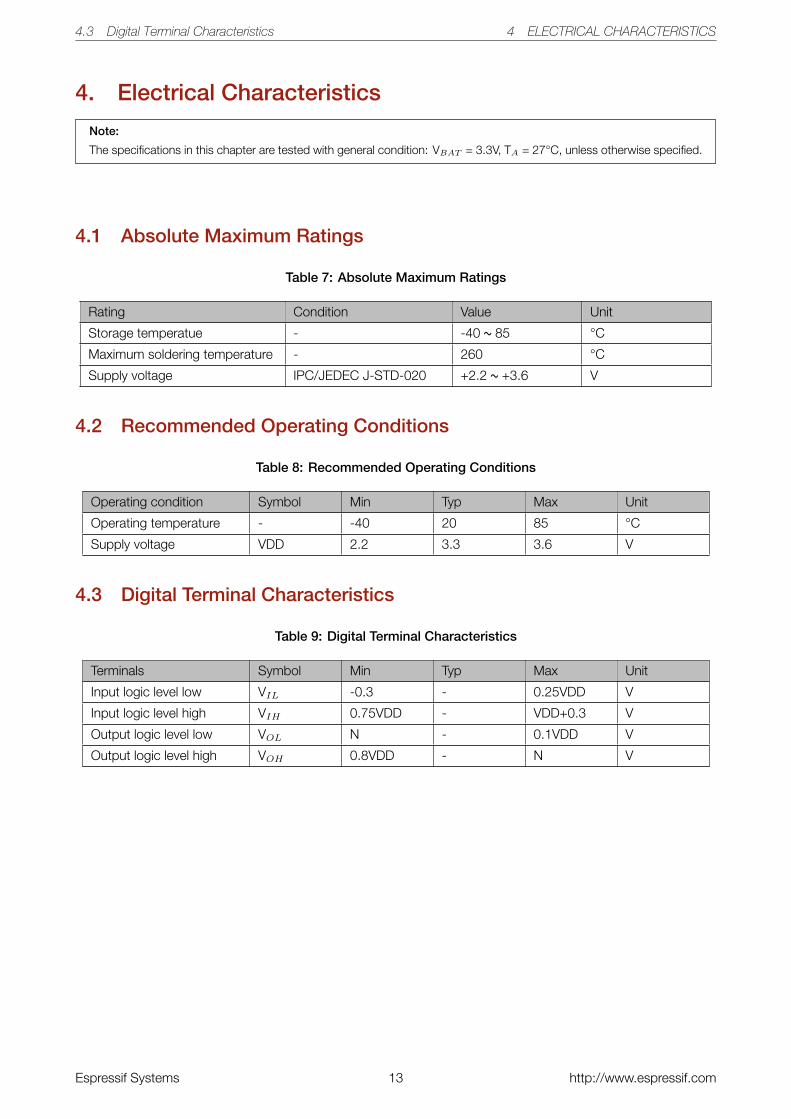
4.1 Absolute Maximum Ratings 13
4.2 Recommended Operating Conditions 13
4.3 Digital Terminal Characteristics 13
4.4 Wi-Fi Radio 14
4.5 Bluetooth LE Radio 14
4.5.1 Receiver 14
4.5.2 Transmit 15
4.6 Reflow Profile 15
5 Schematics 16
List of Tables1 ESP-WROOM-32 Specifications 2
2 ESP-WROOM-32 Dimensions 3
3 ESP-WROOM-32 Pin Definitions 4
4 Strapping Pins 5
5 Power Consumption by Power Modes 7
6 Interface Description 8
7 Absolute Maximum Ratings 13
8 Recommended Operating Conditions 13
9 Digital Terminal Characteristics 13
10 Wi-Fi Radio Characteristics 14
11 Receiver Characteristics - BLE 14
12 Transmit Characteristics - BLE 15
13 Reflow Profile 15

List of Figures1 Top and Side View of ESP-WROOM-32 3
2 ESP-WROOM-32 Schematics 16
1 PREFACE
1. Preface
ESP-WROOM-32 is a powerful, generic WiFi-BT-BLE MCU module that targets a wide variety of applications
ranging from low power sensor networks to the most demanding tasks such as voice encoding, music streaming
and MP3 decoding.
At the core of this module is the ESP32 chip, which is designed to be scalable and adaptive. There are 2 CPU cores
that can be individually controlled or powered, and the clock frequency is adjustable from 80 MHz to 240 MHz. The
user may also power off the CPU and make use of the low power coprocessor to constantly monitor the peripherals
for changes or crossing of thresholds. ESP32 integrates a rich set of peripherals, ranging from capacitive touch
sensors, Hall sensors, low noise sense amplifiers, SD card interface, Ethernet, high speed SDIO/SPI, UART, I2S
and I2C.
The integration of Bluetooth, Bluetooth LE and Wi-Fi ensures that a wide range of applications can be targeted,
and that it is future proof: using Wi-Fi allows a large physical range and direct connection to the internet through a
Wi-Fi router, while using Bluetooth allows the user to conveniently connect to the phone or broadcast low energy
beacons for its detection. The sleep current of the ESP32 chip is less than 5 µA, making it suitable for battery
powered and wearable electronics applications. ESP-WROOM-32 supports data rates up to 150 Mbps, and 22
dBm output power at the PA to ensure the widest physical range. As such the chip does offer industry leading
specifications and the best optimized performance for electronic integration, range and power consumption, and
connectivity.
The operating system chosen for ESP32 is freeRTOS with LWIP; TLS 1.2 with hardware acceleration is built in as
well. Secure (encrypted) over the air (OTA) upgrade is also supported, so that developers can continually upgrade
their products even after their release. New SDK features, tutorials and example applications will be released over
the next few months. The software releases are covered under the ESP32 bug bounty program and any bugs
can be reported to [email protected]. As the SDK of ESP-WROOM-32 or ESP32 is open-source, the
user can build his own platforms and operating systems. For more in-depth discussion of this, the developer can
contact [email protected].
ESP-WROOM-32 has Espressif’s long term support — ESP32 will be covered under Espressif’s longevity program
and be available for the next 12 years. The design of ESP-WROOM-32 will be open-source when it has been fully
optimized. Feedbacks about the module, chip, API or firmware can be sent to [email protected].
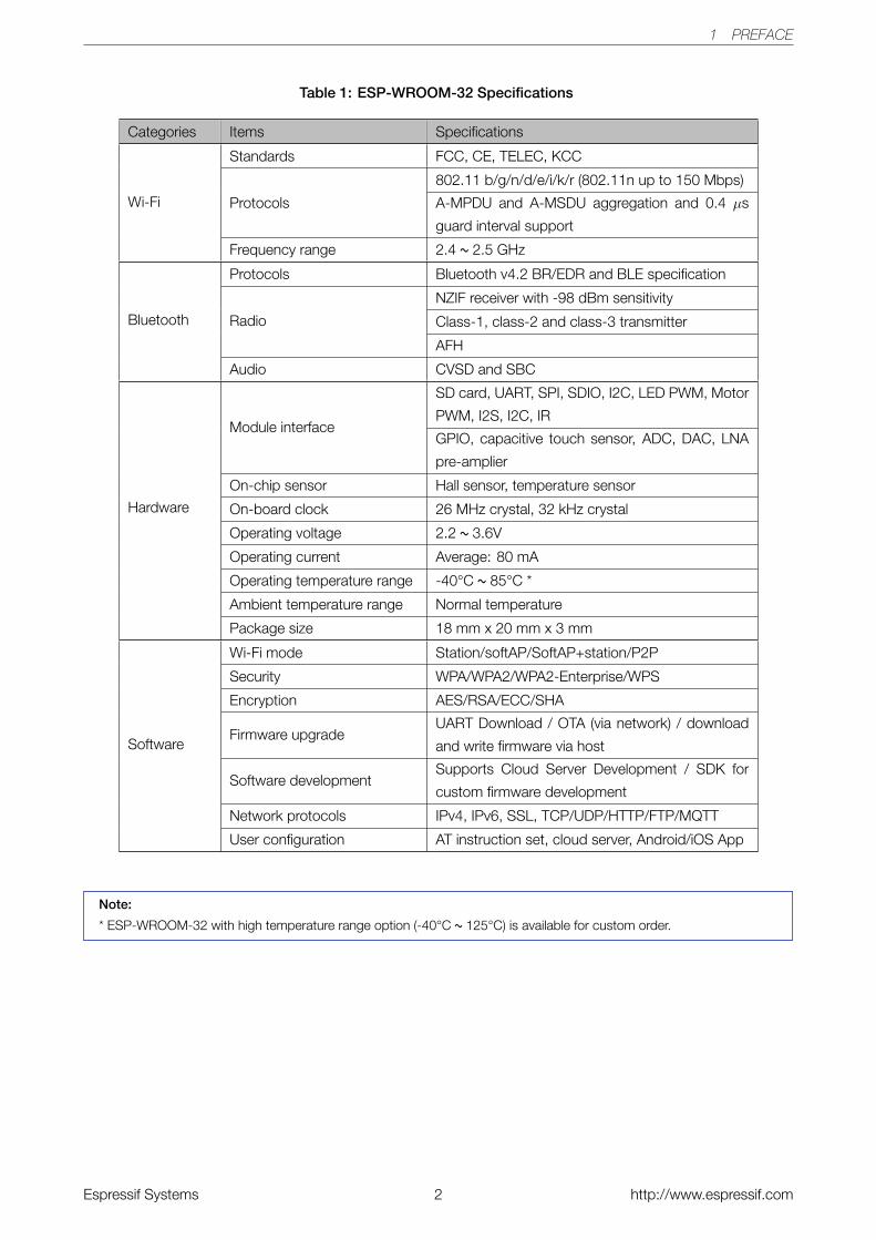
Table 1 provides the specifications of ESP-WROOM-32.
Espressif Systems 1 http://www.espressif.com
1 PREFACE
Table 1: ESP-WROOM-32 Specifications
Categories Items Specifications
Wi-Fi
Standards FCC, CE, TELEC, KCC
Protocols
802.11 b/g/n/d/e/i/k/r (802.11n up to 150 Mbps)
A-MPDU and A-MSDU aggregation and 0.4 µs
guard interval support
Frequency range 2.4 ~ 2.5 GHz
Bluetooth
Protocols Bluetooth v4.2 BR/EDR and BLE specification
Radio
NZIF receiver with -98 dBm sensitivity
Class-1, class-2 and class-3 transmitter
AFH
Audio CVSD and SBC
Hardware
Module interface
SD card, UART, SPI, SDIO, I2C, LED PWM, Motor
PWM, I2S, I2C, IR
GPIO, capacitive touch sensor, ADC, DAC, LNA
pre-amplier
On-chip sensor Hall sensor, temperature sensor
On-board clock 26 MHz crystal, 32 kHz crystal
Operating voltage 2.2 ~ 3.6V
Operating current Average: 80 mA
Operating temperature range -40°C ~ 85°C *
Ambient temperature range Normal temperature
Package size 18 mm x 20 mm x 3 mm
Software
Wi-Fi mode Station/softAP/SoftAP+station/P2P
Security WPA/WPA2/WPA2-Enterprise/WPS
Encryption AES/RSA/ECC/SHA
Firmware upgradeUART Download / OTA (via network) / download
and write firmware via host
Software developmentSupports Cloud Server Development / SDK for
custom firmware development
Network protocols IPv4, IPv6, SSL, TCP/UDP/HTTP/FTP/MQTT
User configuration AT instruction set, cloud server, Android/iOS App
Note:
* ESP-WROOM-32 with high temperature range option (-40°C ~ 125°C) is available for custom order.
Espressif Systems 2 http://www.espressif.com
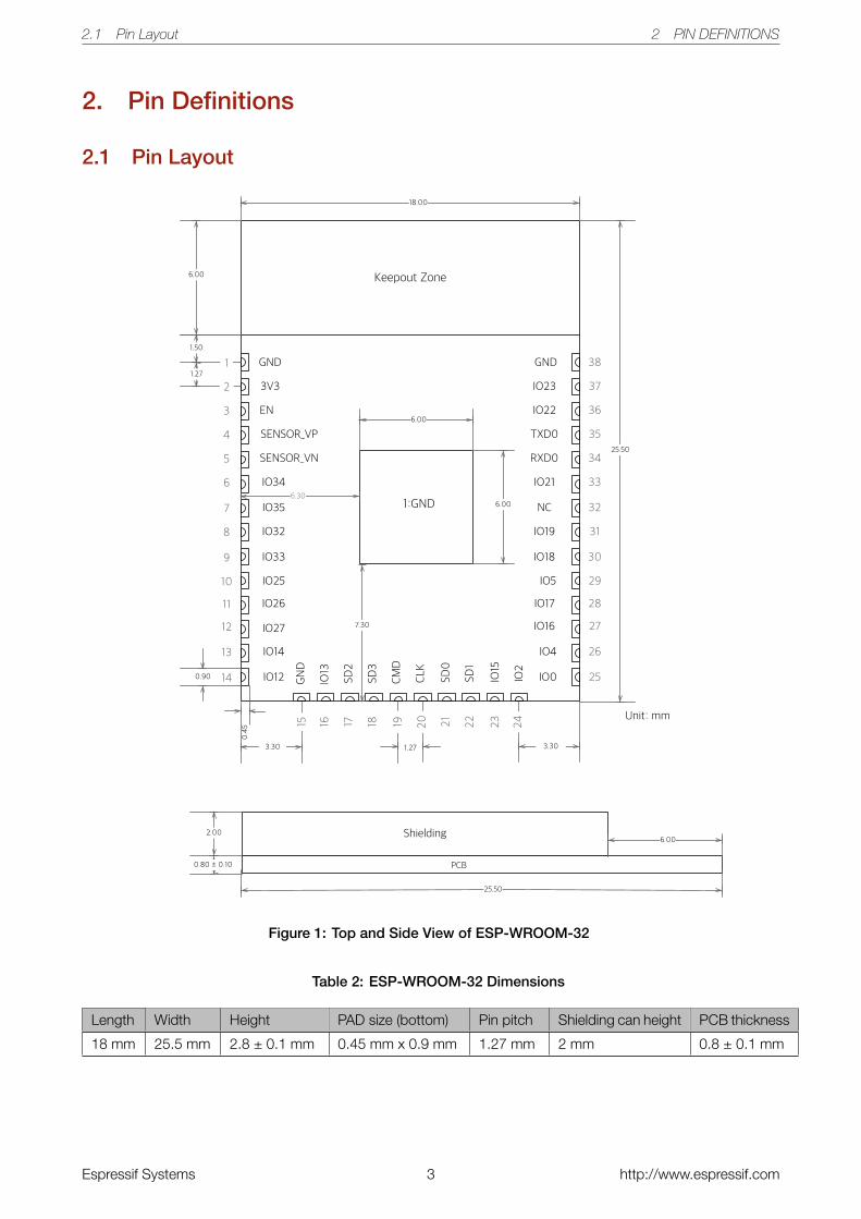
2.1 Pin Layout 2 PIN DEFINITIONS
2. Pin Definitions
2.1 Pin Layout
6.00
18.00
Keepout Zone
1.27
1.50
25.50
3V3
EN
IO14
IO12
IO33
IO25
IO26
IO27
GND
IO32
IO35
IO34
SENSOR_VN
SENSOR_VP
37
36
26
25
30
29
28
27
38
31
32
33
34
35
IO23
IO22
IO4
IO0
IO18
IO5
IO17
IO16
GND
IO19
NC
IO21
RXD0
TXD0
IO13
SD2
IO15
IO2
GND
SD1
SD0
CLK
CMD
SD3
16 17 23222118
Unit: mm
0.45
6.30
6.00
6.00
7.30
0.90
1:GND
2
3
13
14
9
10
11
12
1
8
7
6
5
4
3.301.273.30
15 242019
2.00
0.80 ± 0.10
Shielding
PCB
25.50
6.00
Figure 1: Top and Side View of ESP-WROOM-32
Table 2: ESP-WROOM-32 Dimensions
Length Width Height PAD size (bottom) Pin pitch Shielding can height PCB thickness
18 mm 25.5 mm 2.8 ± 0.1 mm 0.45 mm x 0.9 mm 1.27 mm 2 mm 0.8 ± 0.1 mm
Espressif Systems 3 http://www.espressif.com
2.2 Pin Description 2 PIN DEFINITIONS
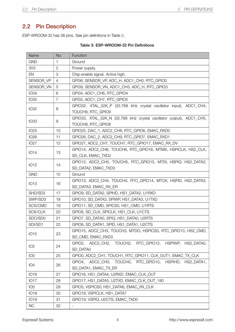
2.2 Pin Description
ESP-WROOM-32 has 38 pins. See pin definitions in Table 3.
Table 3: ESP-WROOM-32 Pin Definitions
Name No. Function
GND 1 Ground
3V3 2 Power supply.
EN 3 Chip-enable signal. Active high.
SENSOR_VP 4 GPI36, SENSOR_VP, ADC_H, ADC1_CH0, RTC_GPIO0
SENSOR_VN 5 GPI39, SENSOR_VN, ADC1_CH3, ADC_H, RTC_GPIO3
IO34 6 GPI34, ADC1_CH6, RTC_GPIO4
IO35 7 GPI35, ADC1_CH7, RTC_GPIO5
IO32 8GPIO32, XTAL_32K_P (32.768 kHz crystal oscillator input), ADC1_CH4,
TOUCH9, RTC_GPIO9
IO33 9GPIO33, XTAL_32K_N (32.768 kHz crystal oscillator output), ADC1_CH5,
TOUCH8, RTC_GPIO8
IO25 10 GPIO25, DAC_1, ADC2_CH8, RTC_GPIO6, EMAC_RXD0
IO26 11 GPIO26, DAC_2, ADC2_CH9, RTC_GPIO7, EMAC_RXD1
IO27 12 GPIO27, ADC2_CH7, TOUCH7, RTC_GPIO17, EMAC_RX_DV
IO14 13GPIO14, ADC2_CH6, TOUCH6, RTC_GPIO16, MTMS, HSPICLK, HS2_CLK,
SD_CLK, EMAC_TXD2
IO12 14GPIO12, ADC2_CH5, TOUCH5, RTC_GPIO15, MTDI, HSPIQ, HS2_DATA2,
SD_DATA2, EMAC_TXD3
GND 15 Ground
IO13 16GPIO13, ADC2_CH4, TOUCH4, RTC_GPIO14, MTCK, HSPID, HS2_DATA3,
SD_DATA3, EMAC_RX_ER
SHD/SD2 17 GPIO9, SD_DATA2, SPIHD, HS1_DATA2, U1RXD
SWP/SD3 18 GPIO10, SD_DATA3, SPIWP, HS1_DATA3, U1TXD
SCS/CMD 19 GPIO11, SD_CMD, SPICS0, HS1_CMD, U1RTS
SCK/CLK 20 GPIO6, SD_CLK, SPICLK, HS1_CLK, U1CTS
SDO/SD0 21 GPIO7, SD_DATA0, SPIQ, HS1_DATA0, U2RTS
SDI/SD1 22 GPIO8, SD_DATA1, SPID, HS1_DATA1, U2CTS
IO15 23GPIO15, ADC2_CH3, TOUCH3, MTDO, HSPICS0, RTC_GPIO13, HS2_CMD,
SD_CMD, EMAC_RXD3
IO2 24GPIO2, ADC2_CH2, TOUCH2, RTC_GPIO12, HSPIWP, HS2_DATA0,
SD_DATA0
IO0 25 GPIO0, ADC2_CH1, TOUCH1, RTC_GPIO11, CLK_OUT1, EMAC_TX_CLK
IO4 26GPIO4, ADC2_CH0, TOUCH0, RTC_GPIO10, HSPIHD, HS2_DATA1,
SD_DATA1, EMAC_TX_ER
IO16 27 GPIO16, HS1_DATA4, U2RXD, EMAC_CLK_OUT
IO17 28 GPIO17, HS1_DATA5, U2TXD, EMAC_CLK_OUT_180
IO5 29 GPIO5, VSPICS0, HS1_DATA6, EMAC_RX_CLK
IO18 30 GPIO18, VSPICLK, HS1_DATA7
IO19 31 GPIO19, VSPIQ, U0CTS, EMAC_TXD0
NC 32 -
Espressif Systems 4 http://www.espressif.com
2.3 Strapping Pins 2 PIN DEFINITIONS
Name No. Function
IO21 33 GPIO21, VSPIHD, EMAC_TX_EN
RXD0 34 GPIO3, U0RXD, CLK_OUT2
TXD0 35 GPIO1, U0TXD, CLK_OUT3, EMAC_RXD2
IO22 36 GPIO22, VSPIWP, U0RTS, EMAC_TXD1
IO23 37 GPIO23, VSPID, HS1_STROBE
GND 38 Ground
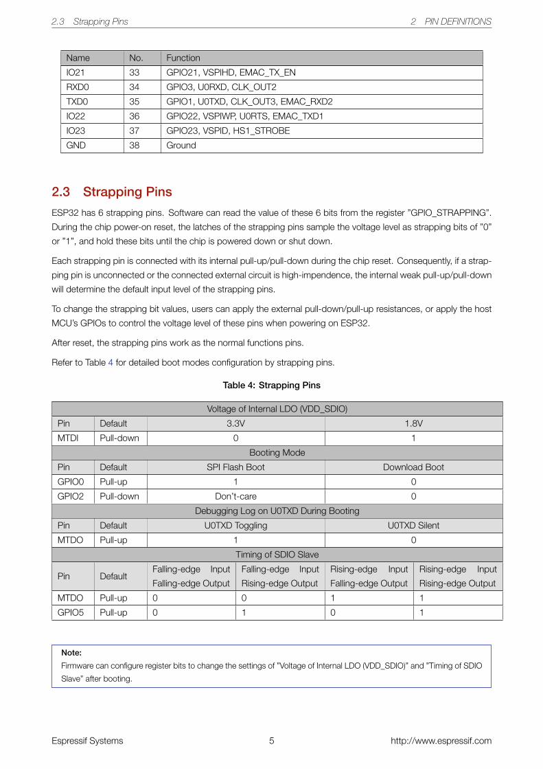
2.3 Strapping Pins
ESP32 has 6 strapping pins. Software can read the value of these 6 bits from the register ”GPIO_STRAPPING”.
During the chip power-on reset, the latches of the strapping pins sample the voltage level as strapping bits of ”0”
or ”1”, and hold these bits until the chip is powered down or shut down.
Each strapping pin is connected with its internal pull-up/pull-down during the chip reset. Consequently, if a strap-
ping pin is unconnected or the connected external circuit is high-impendence, the internal weak pull-up/pull-down
will determine the default input level of the strapping pins.
To change the strapping bit values, users can apply the external pull-down/pull-up resistances, or apply the host
MCU’s GPIOs to control the voltage level of these pins when powering on ESP32.
After reset, the strapping pins work as the normal functions pins.
Refer to Table 4 for detailed boot modes configuration by strapping pins.
Table 4: Strapping Pins
Voltage of Internal LDO (VDD_SDIO)
Pin Default 3.3V 1.8V
MTDI Pull-down 0 1
Booting Mode
Pin Default SPI Flash Boot Download Boot
GPIO0 Pull-up 1 0
GPIO2 Pull-down Don’t-care 0
Debugging Log on U0TXD During Booting
Pin Default U0TXD Toggling U0TXD Silent
MTDO Pull-up 1 0
Timing of SDIO Slave
Pin DefaultFalling-edge Input
Falling-edge Output
Falling-edge Input
Rising-edge Output
Rising-edge Input
Falling-edge Output
Rising-edge Input
Rising-edge Output
MTDO Pull-up 0 0 1 1
GPIO5 Pull-up 0 1 0 1
Note:
Firmware can configure register bits to change the settings of ”Voltage of Internal LDO (VDD_SDIO)” and ”Timing of SDIO
Slave” after booting.
Espressif Systems 5 http://www.espressif.com
3 FUNCTIONAL DESCRIPTION
3. Functional Description
This chapter describes the modules and functions implemented in ESP-WROOM-32.
3.1 CPU and Internal Memory
ESP32 contains two low-power Xtensa® 32-bit LX6 microprocessors. The internal memory includes:
• 448 KBytes ROM for booting and core functions.
• 520 KBytes on-chip SRAM for data and instruction.
• 8 KBytes SRAM in RTC, which is called RTC SLOW Memory and can be accessed by the co-processor
during the deep-sleep mode.
• 8 KBytes SRAM in RTC, which is called RTC FAST Memory and can be used for data storage and accessed
by the main CPU during RTC Boot from the deep-sleep mode.
• 1 Kbit of EFUSE, of which 256 bits are used for the system (MAC address and chip configuration) and the
remaining 768 bits are reserved for customer applications, including Flash-Encryption and Chip-ID.
3.2 External Flash and SRAM
ESP32 supports 4 x 16 MBytes of external QSPI flash and SRAM with hardware encryption based on AES to
protect developer’s programs and data.
ESP32 accesses external QSPI flash and SRAM by the high-speed caches. Up to 16 MBytes of external flash are
memory mapped into the CPU code space, supporting 8, 16 and 32-bit access. Code execution is supported.
Up to 8 MBytes of external SRAM are memory mapped into the CPU data space, supporting 8, 16 and 32-bit
access. Data read is supported on the flash and SRAM. Data write is supported on the SRAM.
3.3 Crystal Oscillators
The frequencies of the main crystal oscillator supported include 40 MHz, 26 MHz and 24 MHz. The accuracy of
crystal oscillators applied should be ±10 PPM, and the operating temperature range -40°C to 85°C.
When using the downloading tools, remember to select the right crystal oscillator type. In circuit design, capac-
itors C1 and C2 that connects to the earth, are added to the input and output terminals of the crystal oscillator
respectively. The values of the two capacitors can be flexible, ranging from 6 pF to 22 pF. However, the specific
capacitive values of C1 and C2 depend on further testing and adjustment of the overall performance of the whole
circuit. Normally, the capacitive values of C1 and C2 are within 10 pF if the crystal oscillator frequency is 26 MHz,
while 10 pF<C1 and C2<22 pF if the crystal oscillator frequency is 40 MHz.
The frequency of the RTC crystal oscillator is typically 32 kHz or 32.768 kHz. The accuracy can be out of the range
of ±20 PPM, since the internal calibration is applied to correct the frequency offset. When the chip operates in low
power modes, the application chooses the external low speed (32 kHz) crystal clock rather than the internal RC
oscillators to achieve the accurate wakeup time.
Espressif Systems 6 http://www.espressif.com
3.4 Power Consumption 3 FUNCTIONAL DESCRIPTION
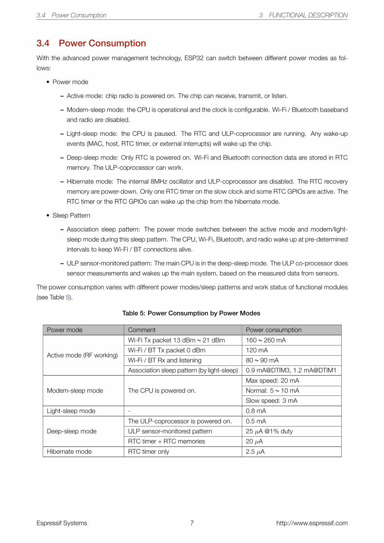
3.4 Power Consumption
With the advanced power management technology, ESP32 can switch between different power modes as fol-
lows:
• Power mode
– Active mode: chip radio is powered on. The chip can receive, transmit, or listen.
– Modem-sleep mode: the CPU is operational and the clock is configurable. Wi-Fi / Bluetooth baseband
and radio are disabled.
– Light-sleep mode: the CPU is paused. The RTC and ULP-coprocessor are running. Any wake-up
events (MAC, host, RTC timer, or external interrupts) will wake up the chip.
– Deep-sleep mode: Only RTC is powered on. Wi-Fi and Bluetooth connection data are stored in RTC
memory. The ULP-coprocessor can work.
– Hibernate mode: The internal 8MHz oscillator and ULP-coprocessor are disabled. The RTC recovery
memory are power-down. Only one RTC timer on the slow clock and some RTC GPIOs are active. The
RTC timer or the RTC GPIOs can wake up the chip from the hibernate mode.
• Sleep Pattern
– Association sleep pattern: The power mode switches between the active mode and modem/light-
sleep mode during this sleep pattern. The CPU, Wi-Fi, Bluetooth, and radio wake up at pre-determined
intervals to keep Wi-Fi / BT connections alive.
– ULP sensor-monitored pattern: The main CPU is in the deep-sleep mode. The ULP co-processor does
sensor measurements and wakes up the main system, based on the measured data from sensors.
The power consumption varies with different power modes/sleep patterns and work status of functional modules
(see Table 5).
Table 5: Power Consumption by Power Modes
Power mode Comment Power consumption
Active mode (RF working)
Wi-Fi Tx packet 13 dBm ~ 21 dBm 160 ~ 260 mA
Wi-Fi / BT Tx packet 0 dBm 120 mA
Wi-Fi / BT Rx and listening 80 ~ 90 mA
Association sleep pattern (by light-sleep) 0.9 mA@DTIM3, 1.2 mA@DTIM1
Modem-sleep mode The CPU is powered on.
Max speed: 20 mA
Normal: 5 ~ 10 mA
Slow speed: 3 mA
Light-sleep mode - 0.8 mA
Deep-sleep mode
The ULP-coprocessor is powered on. 0.5 mA
ULP sensor-monitored pattern 25 µA @1% duty
RTC timer + RTC memories 20 µA
Hibernate mode RTC timer only 2.5 µA
Espressif Systems 7 http://www.espressif.com
3.5 Peripheral Interface Description 3 FUNCTIONAL DESCRIPTION
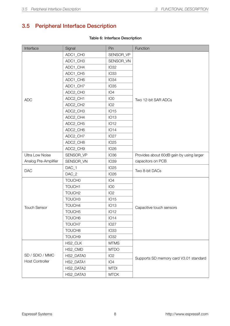
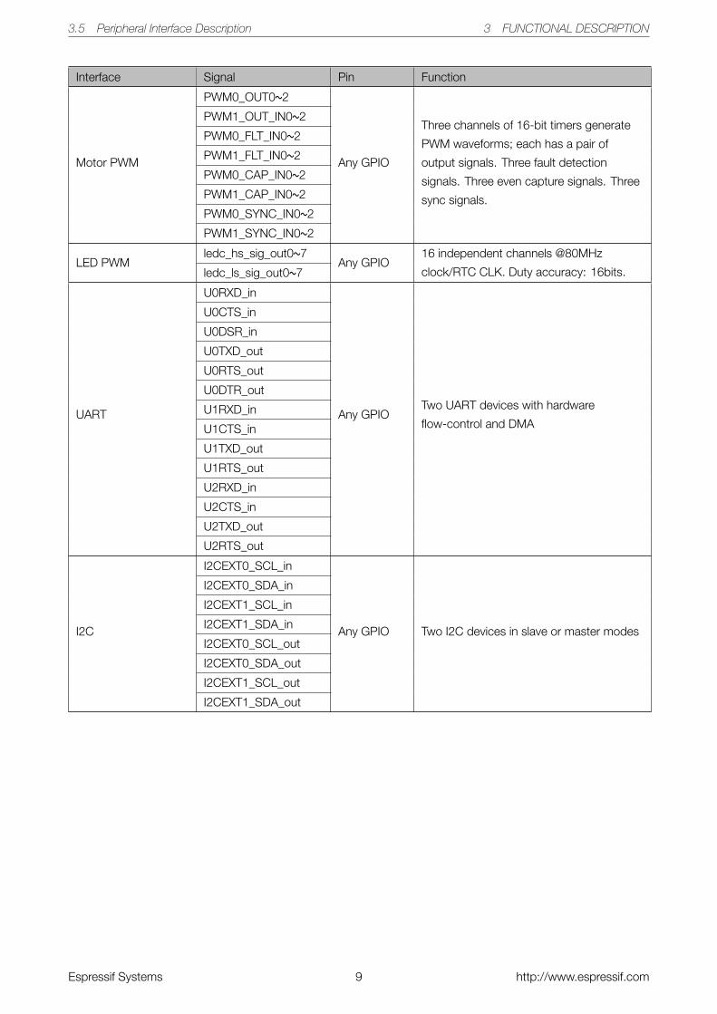
3.5 Peripheral Interface Description
Table 6: Interface Description
Interface Signal Pin Function
ADC
ADC1_CH0 SENSOR_VP
Two 12-bit SAR ADCs
ADC1_CH3 SENSOR_VN
ADC1_CH4 IO32
ADC1_CH5 IO33
ADC1_CH6 IO34
ADC1_CH7 IO35
ADC2_CH0 IO4
ADC2_CH1 IO0
ADC2_CH2 IO2
ADC2_CH3 IO15
ADC2_CH4 IO13
ADC2_CH5 IO12
ADC2_CH6 IO14
ADC2_CH7 IO27
ADC2_CH8 IO25
ADC2_CH9 IO26
Ultra Low Noise
Analog Pre-Amplifier
SENSOR_VP IO36 Provides about 60dB gain by using larger
capacitors on PCBSENSOR_VN IO39
DACDAC_1 IO25
Two 8-bit DACsDAC_2 IO26
Touch Sensor
TOUCH0 IO4
Capacitive touch sensors
TOUCH1 IO0
TOUCH2 IO2
TOUCH3 IO15
TOUCH4 IO13
TOUCH5 IO12
TOUCH6 IO14
TOUCH7 IO27
TOUCH8 IO33
TOUCH9 IO32
SD / SDIO / MMC
Host Controller
HS2_CLK MTMS
Supports SD memory card V3.01 standard
HS2_CMD MTDO
HS2_DATA0 IO2
HS2_DATA1 IO4
HS2_DATA2 MTDI
HS2_DATA3 MTCK
Espressif Systems 8 http://www.espressif.com
3.5 Peripheral Interface Description 3 FUNCTIONAL DESCRIPTION
Interface Signal Pin Function
Motor PWM
PWM0_OUT0~2
Any GPIO
Three channels of 16-bit timers generate
PWM waveforms; each has a pair of
output signals. Three fault detection
signals. Three even capture signals. Three
sync signals.
PWM1_OUT_IN0~2
PWM0_FLT_IN0~2
PWM1_FLT_IN0~2
PWM0_CAP_IN0~2
PWM1_CAP_IN0~2
PWM0_SYNC_IN0~2
PWM1_SYNC_IN0~2
LED PWMledc_hs_sig_out0~7
Any GPIO16 independent channels @80MHz
clock/RTC CLK. Duty accuracy: 16bits.ledc_ls_sig_out0~7
UART
U0RXD_in
Any GPIOTwo UART devices with hardware
flow-control and DMA
U0CTS_in
U0DSR_in
U0TXD_out
U0RTS_out
U0DTR_out
U1RXD_in
U1CTS_in
U1TXD_out
U1RTS_out
U2RXD_in
U2CTS_in
U2TXD_out
U2RTS_out
I2C
I2CEXT0_SCL_in
Any GPIO Two I2C devices in slave or master modes
I2CEXT0_SDA_in
I2CEXT1_SCL_in
I2CEXT1_SDA_in
I2CEXT0_SCL_out
I2CEXT0_SDA_out
I2CEXT1_SCL_out
I2CEXT1_SDA_out
Espressif Systems 9 http://www.espressif.com
3.5 Peripheral Interface Description 3 FUNCTIONAL DESCRIPTION
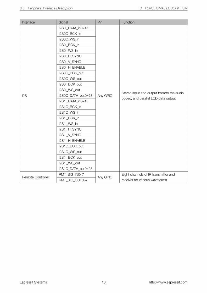
Interface Signal Pin Function
I2S
I2S0I_DATA_in0~15
Any GPIOStereo input and output from/to the audio
codec, and parallel LCD data output
I2S0O_BCK_in
I2S0O_WS_in
I2S0I_BCK_in
I2S0I_WS_in
I2S0I_H_SYNC
I2S0I_V_SYNC
I2S0I_H_ENABLE
I2S0O_BCK_out
I2S0O_WS_out
I2S0I_BCK_out
I2S0I_WS_out
I2S0O_DATA_out0~23
I2S1I_DATA_in0~15
I2S1O_BCK_in
I2S1O_WS_in
I2S1I_BCK_in
I2S1I_WS_in
I2S1I_H_SYNC
I2S1I_V_SYNC
I2S1I_H_ENABLE
I2S1O_BCK_out
I2S1O_WS_out
I2S1I_BCK_out
I2S1I_WS_out
I2S1O_DATA_out0~23
Remote ControllerRMT_SIG_IN0~7
Any GPIOEight channels of IR transmitter and
receiver for various waveformsRMT_SIG_OUT0~7
Espressif Systems 10 http://www.espressif.com
3.5 Peripheral Interface Description 3 FUNCTIONAL DESCRIPTION
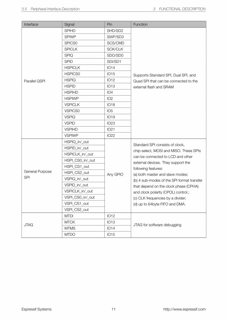
Interface Signal Pin Function
Parallel QSPI
SPIHD SHD/SD2
Supports Standard SPI, Dual SPI, and
Quad SPI that can be connected to the
external flash and SRAM
SPIWP SWP/SD3
SPICS0 SCS/CMD
SPICLK SCK/CLK
SPIQ SDO/SD0
SPID SDI/SD1
HSPICLK IO14
HSPICS0 IO15
HSPIQ IO12
HSPID IO13
HSPIHD IO4
HSPIWP IO2
VSPICLK IO18
VSPICS0 IO5
VSPIQ IO19
VSPID IO23
VSPIHD IO21
VSPIWP IO22
General Purpose
SPI
HSPIQ_in/_out
Any GPIO
Standard SPI consists of clock,
chip-select, MOSI and MISO. These SPIs
can be connected to LCD and other
external devices. They support the
following features:
(a) both master and slave modes;
(b) 4 sub-modes of the SPI format transfer
that depend on the clock phase (CPHA)
and clock polarity (CPOL) control.;
(c) CLK frequencies by a divider;
(d) up to 64byte FIFO and DMA.
HSPID_in/_out
HSPICLK_in/_out
HSPI_CS0_in/_out
HSPI_CS1_out
HSPI_CS2_out
VSPIQ_in/_out
VSPID_in/_out
VSPICLK_in/_out
VSPI_CS0_in/_out
VSPI_CS1_out
VSPI_CS2_out
JTAG
MTDI IO12
JTAG for software debuggingMTCK IO13
MTMS IO14
MTDO IO15
Espressif Systems 11 http://www.espressif.com
3.5 Peripheral Interface Description 3 FUNCTIONAL DESCRIPTION
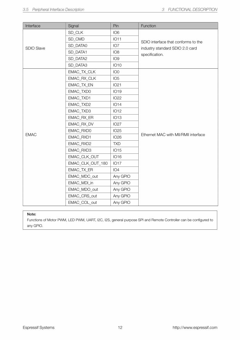
Interface Signal Pin Function
SDIO Slave
SD_CLK IO6
SDIO interface that conforms to the
industry standard SDIO 2.0 card
specification.
SD_CMD IO11
SD_DATA0 IO7
SD_DATA1 IO8
SD_DATA2 IO9
SD_DATA3 IO10
EMAC
EMAC_TX_CLK IO0
Ethernet MAC with MII/RMII interface
EMAC_RX_CLK IO5
EMAC_TX_EN IO21
EMAC_TXD0 IO19
EMAC_TXD1 IO22
EMAC_TXD2 IO14
EMAC_TXD3 IO12
EMAC_RX_ER IO13
EMAC_RX_DV IO27
EMAC_RXD0 IO25
EMAC_RXD1 IO26
EMAC_RXD2 TXD
EMAC_RXD3 IO15
EMAC_CLK_OUT IO16
EMAC_CLK_OUT_180 IO17
EMAC_TX_ER IO4
EMAC_MDC_out Any GPIO
EMAC_MDI_in Any GPIO
EMAC_MDO_out Any GPIO
EMAC_CRS_out Any GPIO
EMAC_COL_out Any GPIO
Note:
Functions of Motor PWM, LED PWM, UART, I2C, I2S, general purpose SPI and Remote Controller can be configured to
any GPIO.
Espressif Systems 12 http://www.espressif.com
4.3 Digital Terminal Characteristics 4 ELECTRICAL CHARACTERISTICS
4. Electrical Characteristics
Note:
The specifications in this chapter are tested with general condition: VBAT = 3.3V, TA = 27°C, unless otherwise specified.
4.1 Absolute Maximum Ratings
Table 7: Absolute Maximum Ratings
Rating Condition Value Unit
Storage temperatue - -40 ~ 85 °C
Maximum soldering temperature - 260 °C
Supply voltage IPC/JEDEC J-STD-020 +2.2 ~ +3.6 V
4.2 Recommended Operating Conditions
Table 8: Recommended Operating Conditions
Operating condition Symbol Min Typ Max Unit
Operating temperature - -40 20 85 °C
Supply voltage VDD 2.2 3.3 3.6 V
4.3 Digital Terminal Characteristics
Table 9: Digital Terminal Characteristics
Terminals Symbol Min Typ Max Unit
Input logic level low VIL -0.3 - 0.25VDD V
Input logic level high VIH 0.75VDD - VDD+0.3 V
Output logic level low VOL N - 0.1VDD V
Output logic level high VOH 0.8VDD - N V
Espressif Systems 13 http://www.espressif.com
4.5 Bluetooth LE Radio 4 ELECTRICAL CHARACTERISTICS
4.4 Wi-Fi Radio
Table 10: Wi-Fi Radio Characteristics
Description Min Typical Max Unit
General Characteristics
Input frequency 2412 - 2484 MHz
Input impedance - 50 - Ω
Input reflection - - -10 dB
Output power of PA 15.5 16.5 21.5 dBm
Sensitivity
DSSS, 1 Mbps - -98 - dBm
CCK, 11 Mbps - -90 - dBm
OFDM, 6 Mbps - -93 - dBm
OFDM, 54 Mbps - -75 - dBm
HT20, MCS0 - -93 - dBm
HT20, MCS7 - -73 - dBm
HT40, MCS0 - -90 - dBm
HT40, MCS7 - -70 - dBm
MCS32 - -91 - dBm
Adjacent Channel Rejection
OFDM, 6 Mbps - 37 - dB
OFDM, 54 Mbps - 21 - dB
HT20, MCS0 - 37 - dB
HT20, MCS7 - 20 - dB
4.5 Bluetooth LE Radio
4.5.1 Receiver
Table 11: Receiver Characteristics - BLE
Parameter Conditions Min Typ Max Unit
Sensitivity @0.1% BER - - -98 - dBm
Maximum received signal @0.1% BER - 0 - - dBm
Co-channel C/I - - +10 - dB
Adjacent channel selectivity C/I
F = F0 + 1 MHz - -5 - dB
F = F0 - 1 MHz - -5 - dB
F = F0 + 2 MHz - -25 - dB
F = F0 - 2 MHz - -35 - dB
F = F0 + 3 MHz - -25 - dB
F = F0 - 3 MHz - -45 - dB
Out-of-band blocking performance
30 MHz - 2000 MHz -10 - - dBm
2000 MHz - 2400 MHz -27 - - dBm
2500 MHz - 3000 MHz -27 - - dBm
3000 MHz - 12.5 GHz -10 - - dBm
Intermodulation - -36 - - dBm
Espressif Systems 14 http://www.espressif.com
4.6 Reflow Profile 4 ELECTRICAL CHARACTERISTICS
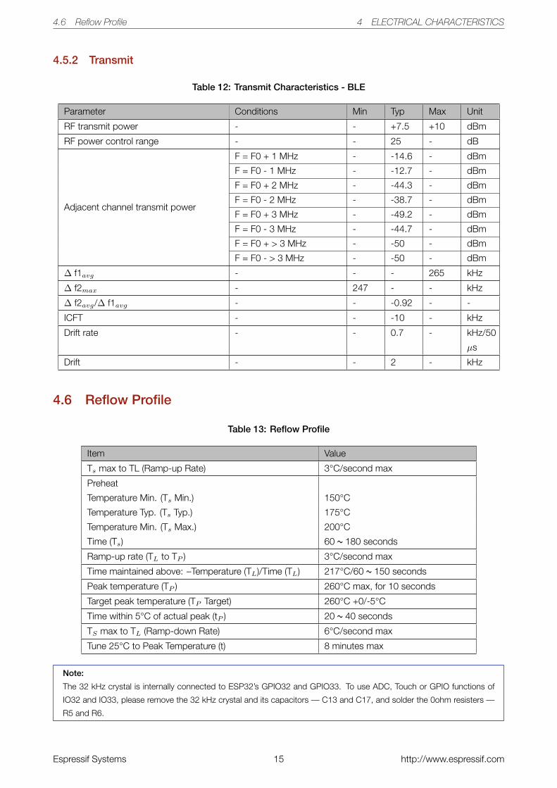
4.5.2 Transmit
Table 12: Transmit Characteristics - BLE
Parameter Conditions Min Typ Max Unit
RF transmit power - - +7.5 +10 dBm
RF power control range - - 25 - dB
Adjacent channel transmit power
F = F0 + 1 MHz - -14.6 - dBm
F = F0 - 1 MHz - -12.7 - dBm
F = F0 + 2 MHz - -44.3 - dBm
F = F0 - 2 MHz - -38.7 - dBm
F = F0 + 3 MHz - -49.2 - dBm
F = F0 - 3 MHz - -44.7 - dBm
F = F0 + > 3 MHz - -50 - dBm
F = F0 - > 3 MHz - -50 - dBm
∆ f1avg - - - 265 kHz
∆ f2max - 247 - - kHz
∆ f2avg/∆ f1avg - - -0.92 - -
ICFT - - -10 - kHz
Drift rate - - 0.7 - kHz/50
µs
Drift - - 2 - kHz
4.6 Reflow Profile
Table 13: Reflow Profile
Item Value
Ts max to TL (Ramp-up Rate) 3°C/second max
Preheat
Temperature Min. (Ts Min.) 150°C
Temperature Typ. (Ts Typ.) 175°C
Temperature Min. (Ts Max.) 200°C
Time (Ts) 60 ~ 180 seconds
Ramp-up rate (TL to TP ) 3°C/second max
Time maintained above: –Temperature (TL)/Time (TL) 217°C/60 ~ 150 seconds
Peak temperature (TP ) 260°C max, for 10 seconds
Target peak temperature (TP Target) 260°C +0/-5°C
Time within 5°C of actual peak (tP ) 20 ~ 40 seconds
TS max to TL (Ramp-down Rate) 6°C/second max
Tune 25°C to Peak Temperature (t) 8 minutes max
Note:
The 32 kHz crystal is internally connected to ESP32’s GPIO32 and GPIO33. To use ADC, Touch or GPIO functions of
IO32 and IO33, please remove the 32 kHz crystal and its capacitors — C13 and C17, and solder the 0ohm resisters —
R5 and R6.
Espressif Systems 15 http://www.espressif.com
5 SCHEMATICS
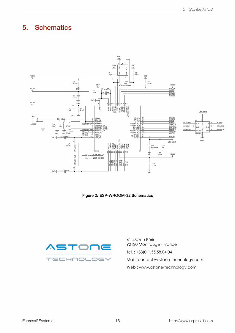
5. Schematics
SDI/SD1SDO/SD0SCK/CLKSCS/CMDSHD/SD3SWP/SD2CHIP_PU
GPIO35
SCK/CLK
SCS/CMD
SWP/SD2 SHD/SD3
SDI/SD1
SDO/SD0
GPIO34
GPI
O25
GPI
O26
GPI
O27
GPI
O14
GPI
O12
GPI
O15
GPI
O13
GPI
O2
GPI
O0
GPIO5GPIO18
GPIO17
GPI
O4
SENSOR_VP
SENSOR_VN
GPIO32
GPIO33
U0RXDGPIO22
GPIO23
GPIO21
GPIO19
U0TXD
GPIO16
GND
GNDGND
GND
GND
VDD33
GND
VDD33
GNDGND
GND
VDD_SDIO
GND
VDD33
GND
VDD33
GND
GND
VDD33
GND
GND
GND GND
GNDGND
VDD_SDIOU4
32kHz
XTA
L32_
IN1
XTA
L32_
OU
T2
R2 NC/0R
C610uF
U1
40MHz+/-10ppm
XIN
1
GN
D2
XO
UT
3
GN
D4
C70.1uF
C80.1uF
C102.4pF
C115pF
C14NC/500pF
R1 20K
C9 6.8pFU3
FLASH
/CS1
DO2
/WP3
GN
D4
DI5
CLK6
/HOLD7
VC
C8
C13 12pF
C40.1uF
C160.1uF
C215pF
ANT1
PCB ANT
12
C510nF
C151uF
C12
270pF
C3100pF
C11
270pF
U2ESP32
VDDA1
LNA_IN2
VDD3P33
VDD3P34
SENSOR_VP5
SENSOR_CAPP6
SENSOR_CAPN7
SENSOR_VN8
CHIP_PU9
VDET_110
VDET_211
32K_XP12
32K
_XN
13
GP
IO25
14
GP
IO26
15
GP
IO27
16
MTM
S17
MTD
I18
VD
D3P
3_R
TC19
MTC
K20
MTD
O21
GP
IO2
22
GP
IO0
23
GP
IO4
24
VDD_SDIO26
GPIO1625
GPIO1727SD_DATA_228SD_DATA_329SD_CMD30SD_CLK31SD_DATA_032
GN
D49
SD_DATA_133GPIO534GPIO1835
GP
IO19
38
CA
P2
47
VD
DA
43X
TAL_
N44
XTA
L_P
45
GPIO2336
U0T
XD
41
GP
IO22
39
GP
IO21
42
VD
D3P
3_C
PU
37
CA
P1
48
VD
DA
46
U0R
XD
40
L11.6nH
R3 NC/0R
C18 3nF
C17 12pF
Figure 2: ESP-WROOM-32 Schematics
Espressif Systems 16 http://www.espressif.com
41-43, rue Périer92120 Montrouge - France
Tel. : +33(0)1.55.58.04.04
Mail : [email protected]
Web : www.astone-technology.com