Embed Size (px)
Citation preview
_______________________________________________________________ Maxim Integrated Products 1
For pricing, delivery, and ordering information, please contact Maxim Direct at 1-888-629-4642, or visit Maxim’s website at www.maxim-ic.com.
MA
X1
71
35
Multi-Output DC-DC Power Supply with VCOM Amplifier and Temperature Sensor for
E-Paper Applications
19-5881; Rev 2; 5/12
Ordering Information
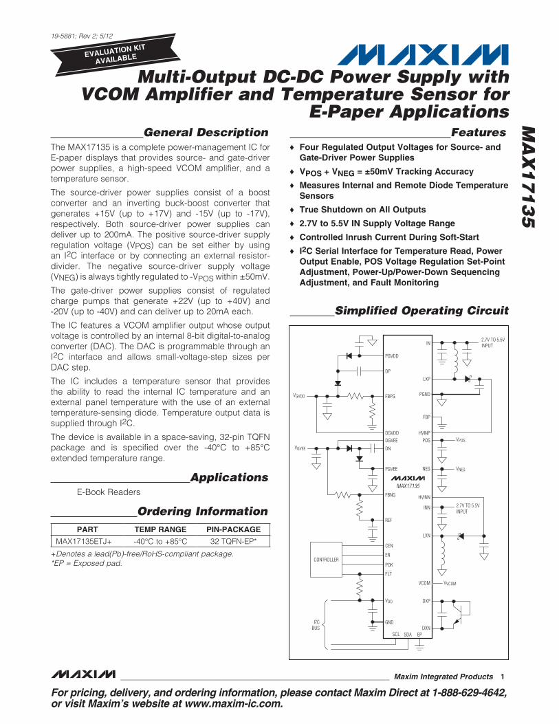
General DescriptionThe MAX17135 is a complete power-management IC for E-paper displays that provides source- and gate-driver power supplies, a high-speed VCOM amplifier, and a temperature sensor.
The source-driver power supplies consist of a boost converter and an inverting buck-boost converter that generates +15V (up to +17V) and -15V (up to -17V), respectively. Both source-driver power supplies can deliver up to 200mA. The positive source-driver supply regulation voltage (VPOS) can be set either by using an I2C interface or by connecting an external resistor- divider. The negative source-driver supply voltage (VNEG) is always tightly regulated to -VPOS within Q50mV.
The gate-driver power supplies consist of regulated charge pumps that generate +22V (up to +40V) and -20V (up to -40V) and can deliver up to 20mA each.
The IC features a VCOM amplifier output whose output voltage is controlled by an internal 8-bit digital-to-analog converter (DAC). The DAC is programmable through an I2C interface and allows small-voltage-step sizes per DAC step.
The IC includes a temperature sensor that provides the ability to read the internal IC temperature and an external panel temperature with the use of an external temperature-sensing diode. Temperature output data is supplied through I2C.
The device is available in a space-saving, 32-pin TQFN package and is specified over the -40NC to +85NC extended temperature range.
ApplicationsE-Book Readers
FeaturesS Four Regulated Output Voltages for Source- and
Gate-Driver Power Supplies
S VPOS + VNEG = ±50mV Tracking Accuracy
S Measures Internal and Remote Diode Temperature Sensors
S True Shutdown on All Outputs
S 2.7V to 5.5V IN Supply Voltage Range
S Controlled Inrush Current During Soft-Start
S I2C Serial Interface for Temperature Read, Power Output Enable, POS Voltage Regulation Set-Point Adjustment, Power-Up/Power-Down Sequencing Adjustment, and Fault Monitoring
+Denotes a lead(Pb)-free/RoHS-compliant package.*EP = Exposed pad.
Simplified Operating Circuit
EVALUATION KIT
AVAILABLE
PGVDD
DP
FBPG
DGVDD
DGVEE
DN
PGVEE
FBNG
REF
CEN
EN
POK
FLT
VDD
GND
SCL SDA EPDXN
DXP
VCOM
LXN
INN
HVINN
NEG
POS
HVINP
FBP
PGND
LXP
IN2.7V TO 5.5VINPUT
VPOS
VNEG
2.7V TO 5.5VINPUT
VVCOM
CONTROLLER
VGVEE
VGVDD
I2CBUS
MAX17135
PART TEMP RANGE PIN-PACKAGE
MAX17135ETJ+ -40NC to +85NC 32 TQFN-EP*
MA
X1
71
35
Multi-Output DC-DC Power Supply with VCOM Amplifier and Temperature Sensor for E-Paper Applications
2
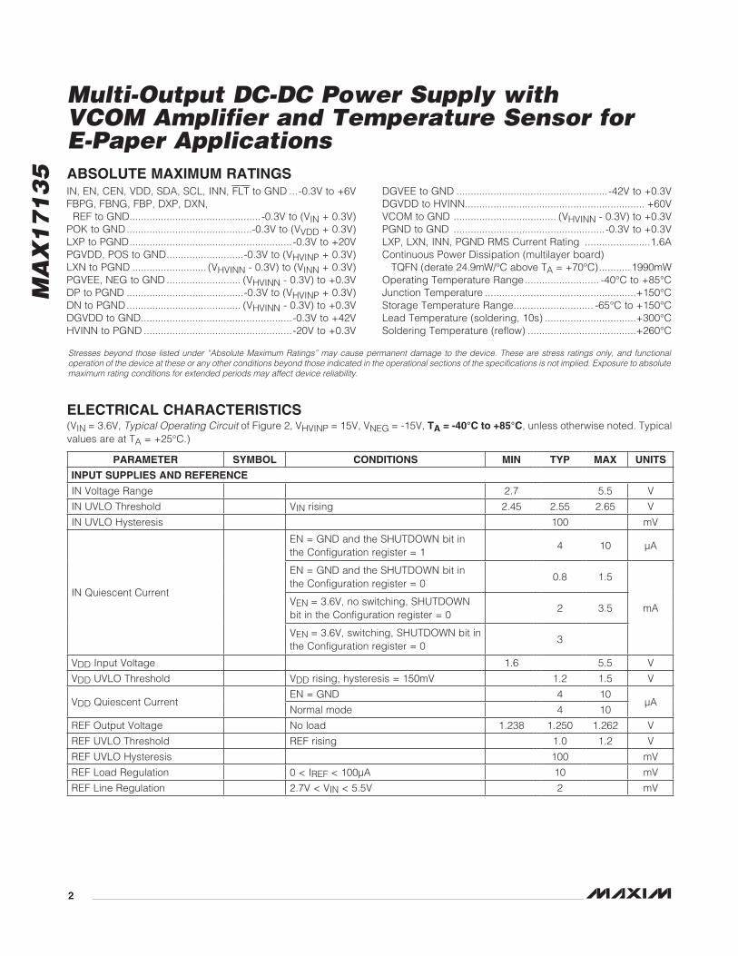
Stresses beyond those listed under “Absolute Maximum Ratings” may cause permanent damage to the device. These are stress ratings only, and functional operation of the device at these or any other conditions beyond those indicated in the operational sections of the specifications is not implied. Exposure to absolute maximum rating conditions for extended periods may affect device reliability.
IN, EN, CEN, VDD, SDA, SCL, INN, FLT to GND ...-0.3V to +6VFBPG, FBNG, FBP, DXP, DXN, REF to GND ..............................................-0.3V to (VIN + 0.3V)POK to GND ............................................-0.3V to (VVDD + 0.3V)LXP to PGND .........................................................-0.3V to +20VPGVDD, POS to GND ...........................-0.3V to (VHVINP + 0.3V)LXN to PGND .......................... (VHVINN - 0.3V) to (VINN + 0.3V)PGVEE, NEG to GND .......................... (VHVINN - 0.3V) to +0.3VDP to PGND .........................................-0.3V to (VHVINP + 0.3V)DN to PGND ........................................ (VHVINN - 0.3V) to +0.3VDGVDD to GND .....................................................-0.3V to +42VHVINN to PGND ....................................................-20V to +0.3V
DGVEE to GND .....................................................-42V to +0.3VDGVDD to HVINN ............................................................... +60VVCOM to GND .................................... (VHVINN - 0.3V) to +0.3VPGND to GND .....................................................-0.3V to +0.3VLXP, LXN, INN, PGND RMS Current Rating .......................1.6AContinuous Power Dissipation (multilayer board) TQFN (derate 24.9mW/NC above TA = +70NC) ........... 1990mWOperating Temperature Range .......................... -40NC to +85NCJunction Temperature .....................................................+150NCStorage Temperature Range ............................ -65NC to +150NCLead Temperature (soldering, 10s) ................................+300NCSoldering Temperature (reflow) ......................................+260NC
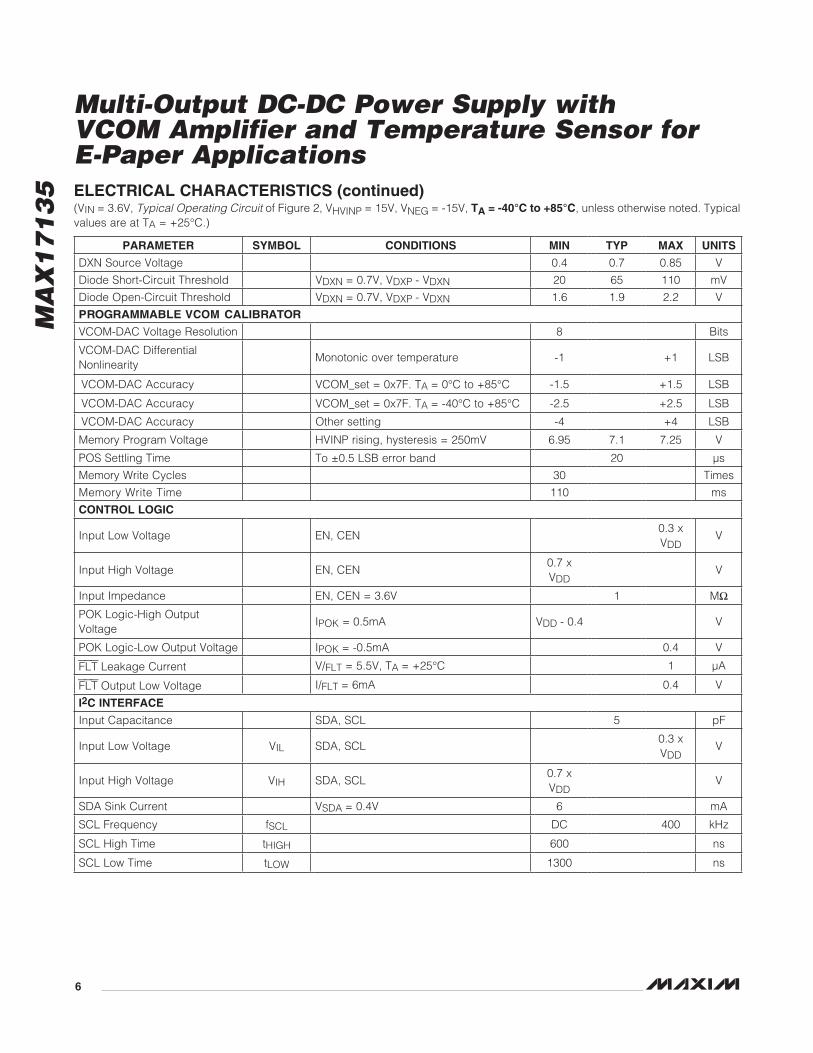
ELECTRICAL CHARACTERISTICS(VIN = 3.6V, Typical Operating Circuit of Figure 2, VHVINP = 15V, VNEG = -15V, TA = -40°C to +85°C, unless otherwise noted. Typical values are at TA = +25NC.)
ABSOLUTE MAXIMUM RATINGS
PARAMETER SYMBOL CONDITIONS MIN TYP MAX UNITS
INPUT SUPPLIES AND REFERENCE
IN Voltage Range 2.7 5.5 V
IN UVLO Threshold VIN rising 2.45 2.55 2.65 V
IN UVLO Hysteresis 100 mV
IN Quiescent Current
EN = GND and the SHUTDOWN bit in the Configuration register = 1
4 10 FA
EN = GND and the SHUTDOWN bit in the Configuration register = 0
0.8 1.5
mAVEN = 3.6V, no switching, SHUTDOWN bit in the Configuration register = 0
2 3.5
VEN = 3.6V, switching, SHUTDOWN bit in the Configuration register = 0
3
VDD Input Voltage 1.6 5.5 V
VDD UVLO Threshold VDD rising, hysteresis = 150mV 1.2 1.5 V
VDD Quiescent Current EN = GND 4 10
FANormal mode 4 10
REF Output Voltage No load 1.238 1.250 1.262 V
REF UVLO Threshold REF rising 1.0 1.2 V
REF UVLO Hysteresis 100 mV
REF Load Regulation 0 < IREF < 100FA 10 mV
REF Line Regulation 2.7V < VIN < 5.5V 2 mV
MA
X1
71
35
Multi-Output DC-DC Power Supply with VCOM Amplifier and Temperature Sensor for
E-Paper Applications
3
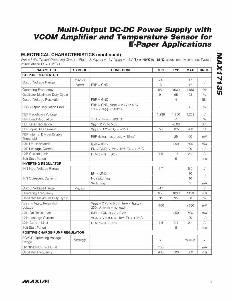
ELECTRICAL CHARACTERISTICS (continued)(VIN = 3.6V, Typical Operating Circuit of Figure 2, VHVINP = 15V, VNEG = -15V, TA = -40°C to +85°C, unless otherwise noted. Typical values are at TA = +25NC.)
PARAMETER SYMBOL CONDITIONS MIN TYP MAX UNITS
STEP-UP REGULATOR
Output Voltage RangeVHVINP VIN 17
VVPOS FBP = GND 5 17
Operating Frequency 850 1000 1150 kHz
Oscillator Maximum Duty Cycle 91 95 98 %
Output Voltage Resolution FBP = GND 4 Bits
POS Output Regulation ErrorFBP = GND, VINN = 2.7V to 5.5V, 1mA < IPOS < 200mA
-2 +2 %
FBP Regulation Voltage 1.238 1.250 1.262 V
FBP Load Regulation 1mA < IPOS < 200mA -1 %
FBP Line Regulation VIN = 2.7V to 5.5V -0.08 %/V
FBP Input Bias Current VFBP = 1.25V, TA = +25NC 50 125 200 nA
FBP Internal Divider Enable Threshold
FBP rising, hysteresis = 10mV 25 50 mV
LXP On-Resistance ILXP = 0.2A 250 500 mI
LXP Leakage Current EN = GND, VLXP = 18V, TA = +25NC 20 FA
LXP Current Limit Duty cycle = 80% 1.5 1.8 2.1 A
Soft-Start Period 5 ms
INVERTING REGULATOR
INN Input Voltage Range 2.7 5.5 V
INN Quiescent Current
EN = GND 10FA
No switching 10
Switching 3 mA
Output Voltage Range VHVINN -17 V
Operating Frequency 850 1000 1150 kHz
Oscillator Maximum Duty Cycle 91 95 98 %
VPOS + VNEG Regulation Voltage
VINN = 2.7V to 5.5V, 1mA < INEG < 200mA, IPOS = no load
-100 +100 mV
LXN On-Resistance INN to LXN, ILXN = 0.2A 250 500 mI
LXN Leakage Current VLXN = VHVINN = -18V, TA = +25NC 20 FA
LXN Current Limit Duty cycle = 85% 1.8 2.1 2.4 A
Soft-Start Period 5 ms
POSITIVE CHARGE-PUMP REGULATOR
PGVDD Operating Voltage Range
VPGVDD 7 VHVINP V
HVINP-DP Current Limit 150 mA
Oscillator Frequency 400 500 600 kHz
MA
X1
71
35
Multi-Output DC-DC Power Supply with VCOM Amplifier and Temperature Sensor for E-Paper Applications
4
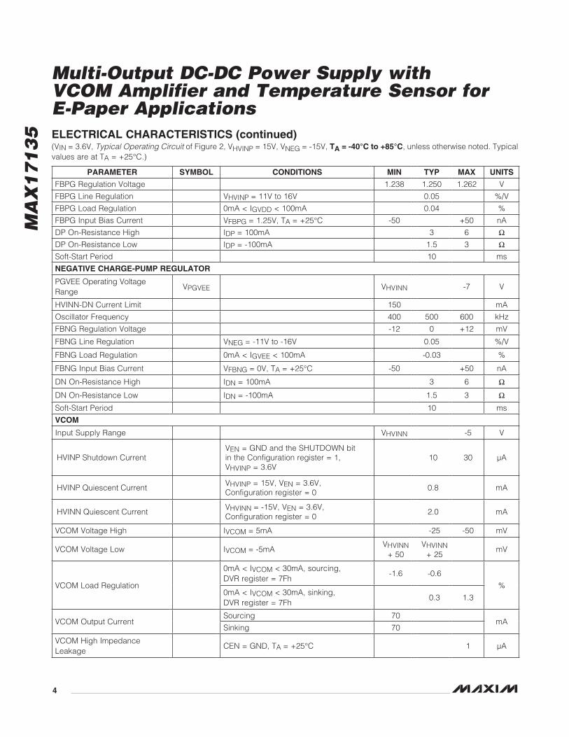
ELECTRICAL CHARACTERISTICS (continued)(VIN = 3.6V, Typical Operating Circuit of Figure 2, VHVINP = 15V, VNEG = -15V, TA = -40°C to +85°C, unless otherwise noted. Typical values are at TA = +25NC.)
PARAMETER SYMBOL CONDITIONS MIN TYP MAX UNITS
FBPG Regulation Voltage 1.238 1.250 1.262 V
FBPG Line Regulation VHVINP = 11V to 16V 0.05 %/V
FBPG Load Regulation 0mA < IGVDD < 100mA 0.04 %
FBPG Input Bias Current VFBPG = 1.25V, TA = +25NC -50 +50 nA
DP On-Resistance High IDP = 100mA 3 6 I
DP On-Resistance Low IDP = -100mA 1.5 3 I
Soft-Start Period 10 ms
NEGATIVE CHARGE-PUMP REGULATOR
PGVEE Operating Voltage Range
VPGVEE VHVINN -7 V
HVINN-DN Current Limit 150 mA
Oscillator Frequency 400 500 600 kHz
FBNG Regulation Voltage -12 0 +12 mV
FBNG Line Regulation VNEG = -11V to -16V 0.05 %/V
FBNG Load Regulation 0mA < IGVEE < 100mA -0.03 %
FBNG Input Bias Current VFBNG = 0V, TA = +25NC -50 +50 nA
DN On-Resistance High IDN = 100mA 3 6 I
DN On-Resistance Low IDN = -100mA 1.5 3 I
Soft-Start Period 10 ms
VCOM
Input Supply Range VHVINN -5 V
HVINP Shutdown CurrentVEN = GND and the SHUTDOWN bit in the Configuration register = 1, VHVINP = 3.6V
10 30 µA
HVINP Quiescent CurrentVHVINP = 15V, VEN = 3.6V, Configuration register = 0
0.8 mA
HVINN Quiescent CurrentVHVINN = -15V, VEN = 3.6V, Configuration register = 0
2.0 mA
VCOM Voltage High IVCOM = 5mA -25 -50 mV
VCOM Voltage Low IVCOM = -5mAVHVINN
+ 50VHVINN
+ 25mV
VCOM Load Regulation
0mA < IVCOM < 30mA, sourcing, DVR register = 7Fh
-1.6 -0.6
%0mA < IVCOM < 30mA, sinking, DVR register = 7Fh
0.3 1.3
VCOM Output CurrentSourcing 70
mASinking 70
VCOM High Impedance Leakage
CEN = GND, TA = +25NC 1 FA
MA
X1
71
35
Multi-Output DC-DC Power Supply with VCOM Amplifier and Temperature Sensor for
E-Paper Applications
5
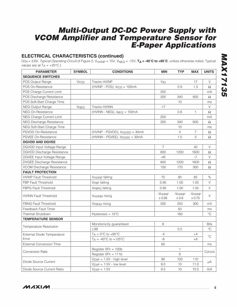
ELECTRICAL CHARACTERISTICS (continued)(VIN = 3.6V, Typical Operating Circuit of Figure 2, VHVINP = 15V, VNEG = -15V, TA = -40°C to +85°C, unless otherwise noted. Typical values are at TA = +25NC.)
PARAMETER SYMBOL CONDITIONS MIN TYP MAX UNITS
SEQUENCE SWITCHES
POS Output Range VPOS Tracks HVINP VIN 17 V
POS On-Resistance (HVINP - POS), IPOS = 100mA 0.9 1.3 I
POS Charge Current Limit 250 mA
POS Discharge Resistance 200 340 600 I
POS Soft-Start Charge Time 10 ms
NEG Output Range VNEG Tracks HVINN -17 V
NEG On-Resistance (HVINN - NEG), INEG = 100mA 0.6 1 I
NEG Charge Current Limit 250 mA
NEG Discharge Resistance 200 340 600 I
NEG Soft-Start Charge Time 10 ms
PGVDD On-Resistance (HVINP - PGVDD), IPGVDD = 30mA 4 7 I
PGVEE On-Resistance (HVINN - PGVEE), IPGVEE = 30mA 1.5 3 I
DGVDD AND DGVEE
DGVDD Input Voltage Range 7 40 V
DGVDD Discharge Resistance 800 1200 1600 I
DGVEE Input Voltage Range -40 -7 V
DVGEE Discharge Resistance 800 1200 1600 I
VCOM Discharge Resistance 100 170 300 I
FAULT PROTECTION
HVINP Fault Threshold VHVINP falling 75 80 85 %
FBP Fault Threshold VFBP falling 0.95 1.00 1.05 V
FBPG Fault Threshold VFBPG falling 0.95 1.00 1.05 V
HVINN Fault Threshold VHVINN rising-VHVINP x 0.85
-VHVINP x 0.8
-VHVINP x 0.75
V
FBNG Fault Threshold VFBNG rising 200 250 300 mV
Feedback Fault Timer 50 ms
Thermal Shutdown Hysteresis = 15NC 160 NC
TEMPERATURE SENSOR
Temperature ResolutionMonotonicity guaranteed 8 Bits
LSB 0.5 NC
External Diode Temperature Error
TA = 0NC to +85NC -4 +4NC
TA = -40NC to +125NC -8 +8
External Conversion Time 60 ms
Conversion RateRegister 0Fh = 100b 1
Conv/sRegister 0Fh = 111b 8
Diode Source CurrentVDXP = 1.5V - high level 90 100 110
FAVDXP = 1.5V - low level 9.0 10 11.0
Diode Source Current Ratio VDXP = 1.5V 9.5 10 10.5 A/A
MA
X1
71
35
Multi-Output DC-DC Power Supply with VCOM Amplifier and Temperature Sensor for E-Paper Applications
6
ELECTRICAL CHARACTERISTICS (continued)(VIN = 3.6V, Typical Operating Circuit of Figure 2, VHVINP = 15V, VNEG = -15V, TA = -40°C to +85°C, unless otherwise noted. Typical values are at TA = +25NC.)
PARAMETER SYMBOL CONDITIONS MIN TYP MAX UNITS
DXN Source Voltage 0.4 0.7 0.85 V
Diode Short-Circuit Threshold VDXN = 0.7V, VDXP - VDXN 20 65 110 mV
Diode Open-Circuit Threshold VDXN = 0.7V, VDXP - VDXN 1.6 1.9 2.2 V
PROGRAMMABLE VCOM CALIBRATOR
VCOM-DAC Voltage Resolution 8 Bits
VCOM-DAC Differential Nonlinearity
Monotonic over temperature -1 +1 LSB
VCOM-DAC Accuracy VCOM_set = 0x7F. TA = 0NC to +85NC -1.5 +1.5 LSB
VCOM-DAC Accuracy VCOM_set = 0x7F. TA = -40NC to +85NC -2.5 +2.5 LSB
VCOM-DAC Accuracy Other setting -4 +4 LSB
Memory Program Voltage HVINP rising, hysteresis = 250mV 6.95 7.1 7.25 V
POS Settling Time To Q0.5 LSB error band 20 Fs
Memory Write Cycles 30 Times
Memory Write Time 110 ms
CONTROL LOGIC
Input Low Voltage EN, CEN0.3 x VDD
V
Input High Voltage EN, CEN0.7 x VDD
V
Input Impedance EN, CEN = 3.6V 1 MI
POK Logic-High Output Voltage
IPOK = 0.5mA VDD - 0.4 V
POK Logic-Low Output Voltage IPOK = -0.5mA 0.4 V
FLT Leakage Current V/FLT = 5.5V, TA = +25NC 1 FA
FLT Output Low Voltage I/FLT = 6mA 0.4 V
I2C INTERFACE
Input Capacitance SDA, SCL 5 pF
Input Low Voltage VIL SDA, SCL0.3 x VDD
V
Input High Voltage VIH SDA, SCL0.7 x VDD
V
SDA Sink Current VSDA = 0.4V 6 mA
SCL Frequency fSCL DC 400 kHz
SCL High Time tHIGH 600 ns
SCL Low Time tLOW 1300 ns
MA
X1
71
35
Multi-Output DC-DC Power Supply with VCOM Amplifier and Temperature Sensor for
E-Paper Applications
7
Note 1: Holding the SDA line low for a time greater than tTIMEOUT causes the device to reset SDA to the IDLE state of the serial bus communication (SDA set high).
Note 2: Guaranteed by design, not production tested.Note 3: All devices are 100% tested at TA = +25°C. Limits over temperature are guaranteed by design.
ELECTRICAL CHARACTERISTICS (continued)(VIN = 3.6V, Typical Operating Circuit of Figure 2, VHVINP = 15V, VNEG = -15V, TA = -40°C to +85°C, unless otherwise noted. Typical values are at TA = +25NC.)
Figure 1. Timing Definitions Used in the Electrical Characteristics
SCL
SDAVIH
VIL
tF
tHD;STA tR
tLOWtHIGH
tHD;DATtSU;DAT tSU;STA
tSU;STO
tBUF
PARAMETER SYMBOL CONDITIONS MIN TYP MAX UNITS
SDA, SCL Rise Time tRCBUS = total bus line capacitance (pF) (Note 2)
20 + 10 x CBUS
300 ns
SDA, SCL Fall Time tFCBUS = total bus line capacitance (pF) (Note 2)
20 + 10 x CBUS
300 ns
START Hold Time tHD;STA 10% of SDA to 90% of SCL 600 ns
START Setup Time tSU;STA 600 ns
Data Input Hold Time tHD;DAT 0 ns
Data Input Setup Time tSU;DAT 100 ns
STOP Setup Time tSU;STO 600 ns
Bus Free Time tBUF 1300 ns
Input Spike Suppression SDA, SCL (Note 2) 250 ns
SDA Reset Low Time tTIMEOUT (Notes 1, 2) 60 ms
MA
X1
71
35
8
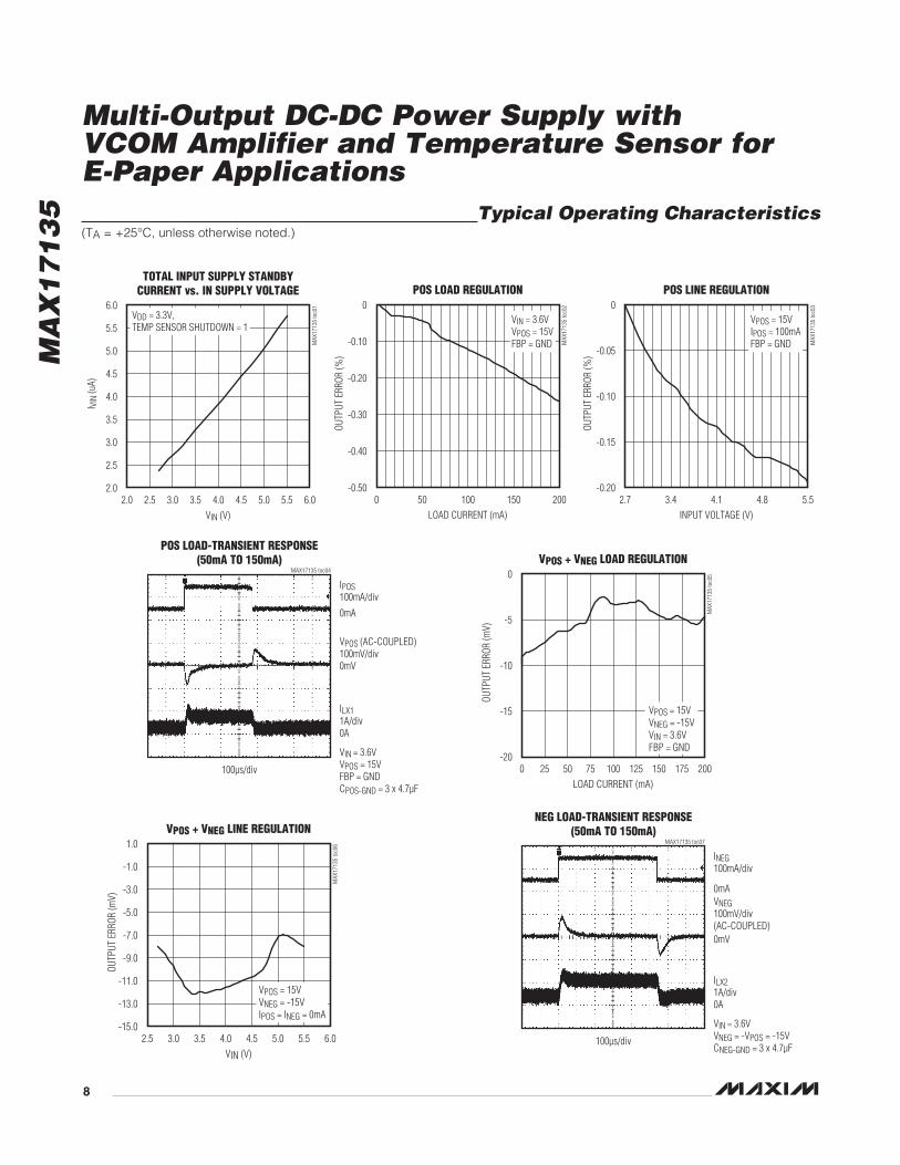
Multi-Output DC-DC Power Supply with VCOM Amplifier and Temperature Sensor for E-Paper Applications Typical Operating Characteristics(TA = +25°C, unless otherwise noted.)
TOTAL INPUT SUPPLY STANDBYCURRENT vs. IN SUPPLY VOLTAGE
MAX
1713
5 to
c01
VIN (V)
I VIN
(uA)
5.55.02.5 3.0 3.5 4.0 4.5
2.5
3.0
3.5
4.0
4.5
5.0
5.5
6.0
2.02.0 6.0
VDD = 3.3V,TEMP SENSOR SHUTDOWN = 1
POS LOAD REGULATION
MAX
1713
5 to
c02
LOAD CURRENT (mA)
OUTP
UT E
RROR
(%)
15010050
-0.40
-0.30
-0.20
-0.10
0
-0.500 200
VIN = 3.6VVPOS = 15VFBP = GND
POS LINE REGULATION
MAX
1713
5 to
c03
INPUT VOLTAGE (V)
OUTP
UT E
RROR
(%)
4.84.13.4
-0.15
-0.10
-0.05
0
-0.202.7 5.5
VPOS = 15VIPOS = 100mAFBP = GND
POS LOAD-TRANSIENT RESPONSE(50mA TO 150mA)
MAX17135 toc04
IPOS100mA/div
VPOS (AC-COUPLED)100mV/div
0mA
0mV
0A
ILX11A/div
VIN = 3.6VVPOS = 15VFBP = GNDCPOS-GND = 3 x 4.7µF
100µs/div
VPOS + VNEG LINE REGULATION
MAX
1713
5 to
c06
VIN (V)
OUTP
UT E
RROR
(mV)
5.55.03.0 3.5 4.0 4.5
-13.0
-11.0
-9.0
-7.0
-5.0
-3.0
-1.0
1.0
-15.02.5 6.0
VPOS = 15VVNEG = -15VIPOS = INEG = 0mA
VPOS + VNEG LOAD REGULATION
MAX
1713
5 to
c05
LOAD CURRENT (mA)
OUTP
UT E
RROR
(mV)
175150125100755025
-15
-10
-5
0
-200 200
VPOS = 15VVNEG = -15VVIN = 3.6VFBP = GND
NEG LOAD-TRANSIENT RESPONSE(50mA TO 150mA)
MAX17135 toc07
INEG100mA/div
VNEG100mV/div(AC-COUPLED)
0mA
0mV
0A
ILX21A/div
VIN = 3.6VVNEG = -VPOS = -15VCNEG-GND = 3 x 4.7µF
100µs/div
MA
X1
71
35
9
Multi-Output DC-DC Power Supply with VCOM Amplifier and Temperature Sensor for
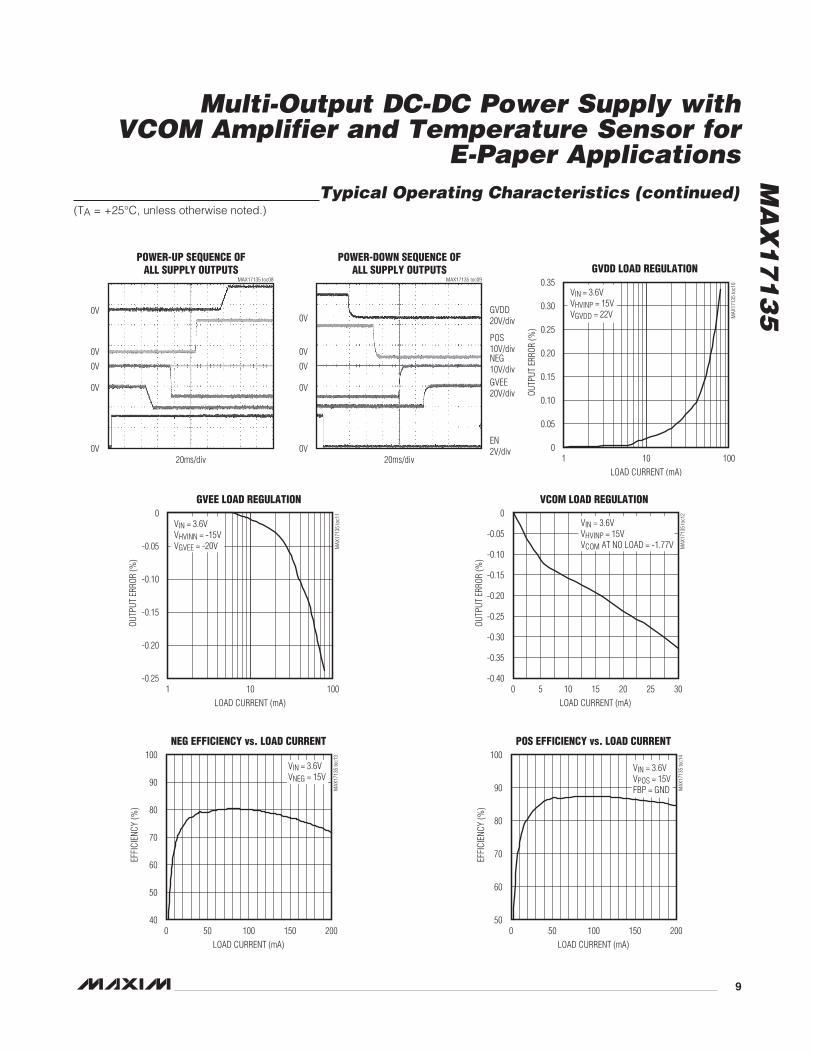
E-Paper Applications Typical Operating Characteristics (continued)(TA = +25°C, unless otherwise noted.)
POWER-UP SEQUENCE OFALL SUPPLY OUTPUTS
MAX17135 toc08
0V
0V
0V
0V
0V
20ms/div
POWER-DOWN SEQUENCE OFALL SUPPLY OUTPUTS
MAX17135 toc09
0V
0V
0V
0V
0V
20ms/div
GVDD20V/div
POS10V/divNEG10V/divGVEE20V/div
EN2V/div
GVDD LOAD REGULATION
MAX
1713
5 to
c10
LOAD CURRENT (mA)
OUTP
UT E
RROR
(%)
10
0.05
0.10
0.15
0.20
0.25
0.30
0.35
01 100
VIN = 3.6VVHVINP = 15VVGVDD = 22V
GVEE LOAD REGULATION
MAX
1713
5 to
c11
LOAD CURRENT (mA)
OUTP
UT E
RROR
(%)
10
-0.20
-0.15
-0.10
-0.05
0
-0.251 100
VIN = 3.6VVHVINN = -15VVGVEE = -20V
NEG EFFICIENCY vs. LOAD CURRENT
MAX
1713
5 to
c13
LOAD CURRENT (mA)
EFFI
CIEN
CY (%
)
15010050
60
70
80
90
100
40
50
0 200
VIN = 3.6VVNEG = 15V
VCOM LOAD REGULATION
MAX
1713
5 to
c12
LOAD CURRENT (mA)
OUTP
UT E
RROR
(%)
5 15 2010 25
-0.35
-0.30
-0.25
-0.20
-0.15
-0.10
-0.05
0
-0.400 30
VIN = 3.6VVHVINP = 15VVCOM AT NO LOAD = -1.77V
POS EFFICIENCY vs. LOAD CURRENT
MAX
1713
5 to
c14
LOAD CURRENT (mA)
EFFI
CIEN
CY (%
)
15010050
60
70
80
90
100
500 200
VIN = 3.6VVPOS = 15VFBP = GND
MA
X1
71
35
10
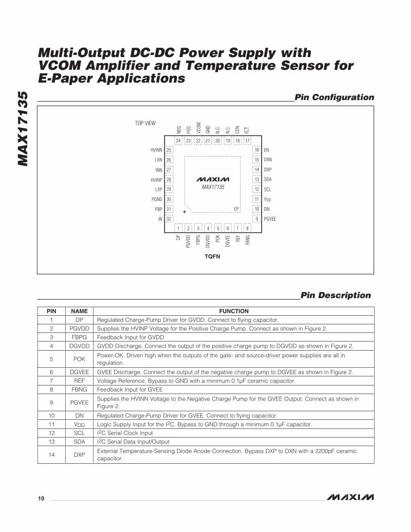
Multi-Output DC-DC Power Supply with VCOM Amplifier and Temperature Sensor for E-Paper Applications Pin Configuration
Pin Description
MAX17135
TQFN
TOP VIEW
29
30
28
27
12
11
13
PGVD
D
DGVD
D
POK
DGVE
E
REF
14
DP
POS
GND
N.C.
NEG
N.C.
CEN
1 2
HVINP
4 5 6 7
2324 22 20 19 18
LXP
PGND
DXP
SDA
SCL
VDDFB
PGVC
OM
3
21
31 10FBP DN
32 9IN PGVEE
EP+
INN
26 15 DXNLXN
25 16 EN
FBNG
FLT
8
17
HVINN
PIN NAME FUNCTION
1 DP Regulated Charge-Pump Driver for GVDD. Connect to flying capacitor.
2 PGVDD Supplies the HVINP Voltage for the Positive Charge Pump. Connect as shown in Figure 2.
3 FBPG Feedback Input for GVDD
4 DGVDD GVDD Discharge. Connect the output of the positive charge pump to DGVDD as shown in Figure 2.
5 POKPower-OK. Driven high when the outputs of the gate- and source-driver power supplies are all in regulation.
6 DGVEE GVEE Discharge. Connect the output of the negative charge pump to DGVEE as shown in Figure 2.
7 REF Voltage Reference. Bypass to GND with a minimum 0.1FF ceramic capacitor.
8 FBNG Feedback Input for GVEE
9 PGVEESupplies the HVINN Voltage to the Negative Charge Pump for the GVEE Output. Connect as shown in Figure 2.
10 DN Regulated Charge-Pump Driver for GVEE. Connect to flying capacitor.
11 VDD Logic Supply Input for the I2C. Bypass to GND through a minimum 0.1FF capacitor.
12 SCL I2C Serial Clock Input
13 SDA I2C Serial Data Input/Output
14 DXPExternal Temperature-Sensing Diode Anode Connection. Bypass DXP to DXN with a 2200pF ceramic capacitor.
MA
X1
71
35
Multi-Output DC-DC Power Supply with VCOM Amplifier and Temperature Sensor for
E-Paper Applications
11
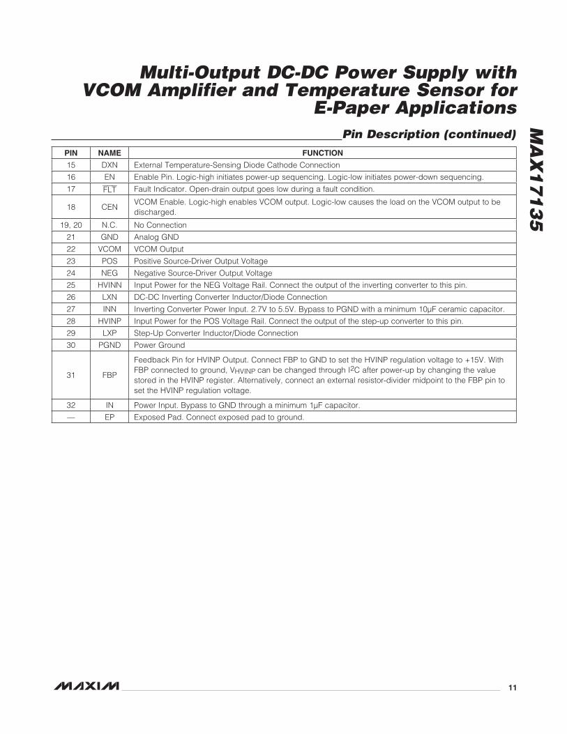
Pin Description (continued)PIN NAME FUNCTION
15 DXN External Temperature-Sensing Diode Cathode Connection
16 EN Enable Pin. Logic-high initiates power-up sequencing. Logic-low initiates power-down sequencing.
17 FLT Fault Indicator. Open-drain output goes low during a fault condition.
18 CENVCOM Enable. Logic-high enables VCOM output. Logic-low causes the load on the VCOM output to be discharged.
19, 20 N.C. No Connection
21 GND Analog GND
22 VCOM VCOM Output
23 POS Positive Source-Driver Output Voltage
24 NEG Negative Source-Driver Output Voltage
25 HVINN Input Power for the NEG Voltage Rail. Connect the output of the inverting converter to this pin.
26 LXN DC-DC Inverting Converter Inductor/Diode Connection
27 INN Inverting Converter Power Input. 2.7V to 5.5V. Bypass to PGND with a minimum 10FF ceramic capacitor.
28 HVINP Input Power for the POS Voltage Rail. Connect the output of the step-up converter to this pin.
29 LXP Step-Up Converter Inductor/Diode Connection
30 PGND Power Ground
31 FBP
Feedback Pin for HVINP Output. Connect FBP to GND to set the HVINP regulation voltage to +15V. With FBP connected to ground, VHVINP can be changed through I2C after power-up by changing the value stored in the HVINP register. Alternatively, connect an external resistor-divider midpoint to the FBP pin to set the HVINP regulation voltage.
32 IN Power Input. Bypass to GND through a minimum 1FF capacitor.
— EP Exposed Pad. Connect exposed pad to ground.
MA
X1
71
35
Multi-Output DC-DC Power Supply with VCOM Amplifier and Temperature Sensor for E-Paper Applications
12
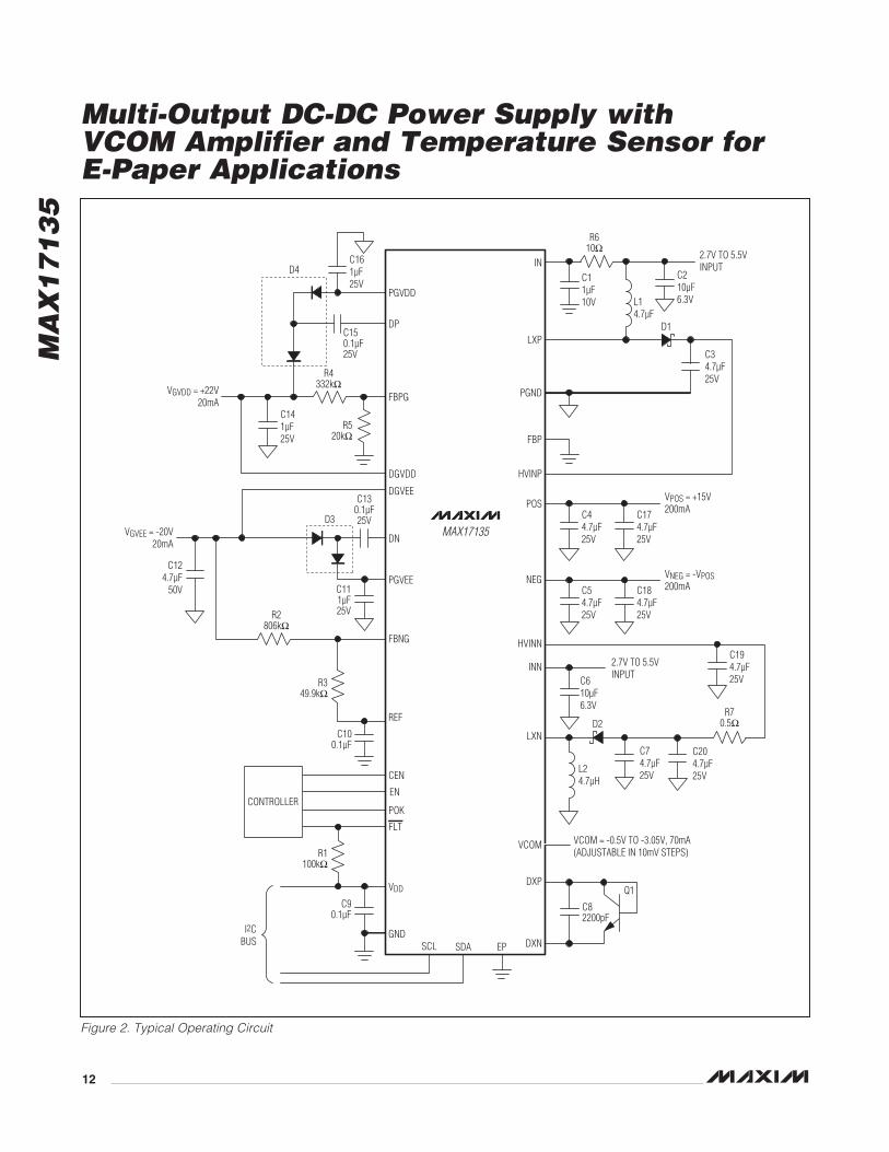
Figure 2. Typical Operating Circuit
PGVDD
D4
D3
C130.1µF25V
C111µF25VR2
806kI
R349.9kI
R610I
R70.5I
C100.1µF
R1100kI
C90.1µF
C82200pF
Q1
C161µF25V
C150.1µF25V
C141µF25V
R4332kI
R520kI
DP
FBPG
DGVDD
DGVEE
DN
PGVEE
FBNG
REF
CEN
EN
POK
FLT
VDD
GNDSCL SDA EP DXN
DXP
VCOM
LXN
INN
HVINN
NEG
POS
HVINP
FBP
PGND
LXP
IN2.7V TO 5.5VINPUT
VPOS = +15V200mA
C34.7µF25V
D1
L14.7µF
C210µF6.3V
C11µF10V
VNEG = -VPOS200mA
2.7V TO 5.5VINPUT
C54.7µF25V
C44.7µF25V
C184.7µF25V
C194.7µF25V
C174.7µF25V
VCOM = -0.5V TO -3.05V, 70mA(ADJUSTABLE IN 10mV STEPS)
L24.7µH
C74.7µF25V
C204.7µF25V
D2
C610µF6.3V
CONTROLLER
VGVDD = +22V20mA
VGVEE = -20V20mA
C124.7µF
50V
I2CBUS
MAX17135
MA
X1
71
35
Multi-Output DC-DC Power Supply with VCOM Amplifier and Temperature Sensor for
E-Paper Applications
13
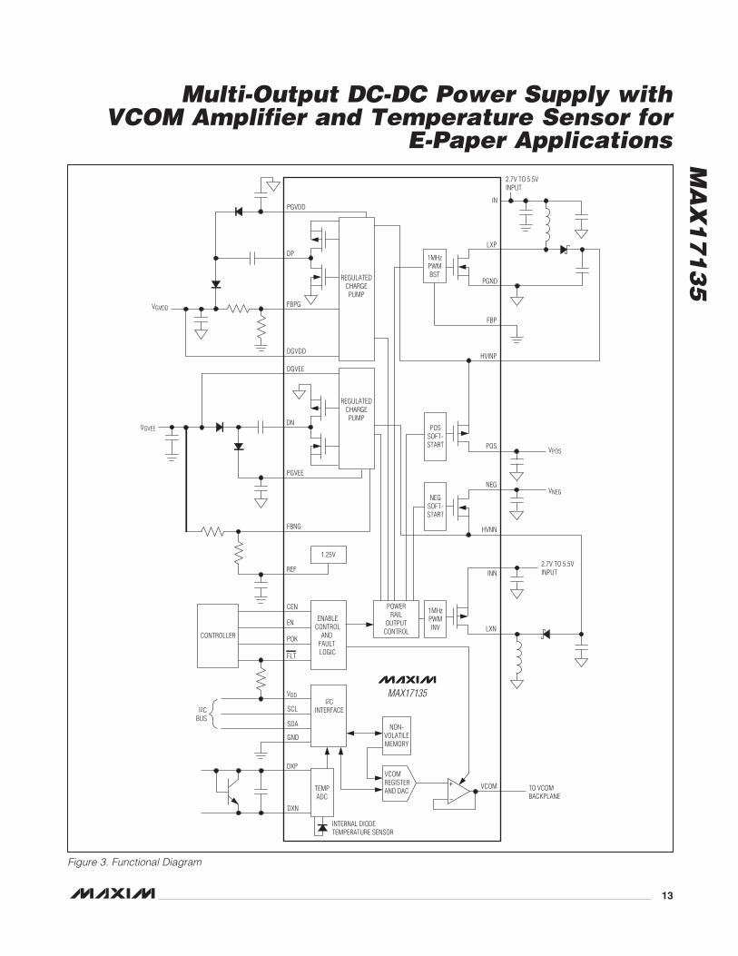
Figure 3. Functional Diagram
PGVDD
DP
FBPG
DGVDD
DGVEE
REGULATEDCHARGEPUMP
DN
PGVEE
FBNG
1.25V
REF
CEN
EN
POK
FLT
VDD
SCL
SDA
GND
DXP
DXN
TEMPADC
INTERNAL DIODETEMPERATURE SENSOR
VCOMREGISTERAND DAC
NON-VOLATILEMEMORY
I2CINTERFACE
ENABLECONTROL
AND FAULT LOGIC
POWERRAIL
OUTPUTCONTROL
1MHzPWMINV
NEGSOFT-START
POSSOFT-START
1MHzPWMBSTREGULATED
CHARGEPUMP
PGND
LXP
IN
2.7V TO 5.5VINPUT
2.7V TO 5.5VINPUT
FBP
HVINP
POS
NEG
HVNN
INN
LXN
VCOM TO VCOMBACKPLANE
VPOS
VNEG
CONTROLLER
I2CBUS
VGVEE
VGVDD
MAX17135
MA
X1
71
35
Multi-Output DC-DC Power Supply with VCOM Amplifier and Temperature Sensor for E-Paper Applications
14
Typical Operating CircuitThe IC’s typical operating circuit (Figure 2) generates Q15V source-driver supplies and +22V and -20V gate-driver supplies for E-paper displays. The input voltage range for the IC is from 2.7V to 5.5V. Figure 3 shows the functional diagram. Table 1 lists recommended compo-nents and Table 2 lists contact information for compo-nent suppliers.
Detailed DescriptionSource-Driver Power Supplies
The source-driver power supplies consist of a boost converter and an inverting buck-boost converter that generate +15V (+17V max) and -15V (-17V max), respectively, and can deliver up to 200mA. The positive source-driver power supply’s regulation voltage (VPOS) can be set using the external resistor-divider network shown in Figure 2, or can be programmed through the I2C interface connecting FBP to GND before power-up.
The negative source-driver supply voltage (VNEG) is automatically tightly regulated to -VPOS within Q50mV. VNEG cannot be adjusted independently of VPOS.
Gate-Driver Power SuppliesThe positive gate-driver power supply (GVDD) generates +22V (+40V max) and the negative gate-driver power supply (GVEE) generates -20V (-40V max). Both supplies can supply up to 20mA current. The GVDD and GVEE regulation voltages are both set by using the external resistor-divider networks shown in Figure 2.
VCOM AmplifierThe IC features a negative output VCOM amplifier whose voltage is programmed through an I2C interface. An internal 8-bit digital-to-analog converter (DAC) allows for a wide VCOM output range of -0.5V to -3.05V and a 10mV change per DAC step. The user can store the DAC setting in nonvolatile memory. On power-up, the nonvola-tile memory sets the DAC to the last stored setting.
Temperature SensorThe IC includes a temperature sensor that reads the internal IC temperature and the external panel tem-perature with the use of an external temperature-sensing diode. Temperature output data is supplied through I2C. An analog-to-digital converter (ADC) converts the tem-perature data to 9 bits, two’s-complement format and stores the conversion results in separate temperature registers.
Fault ProtectionThe IC has robust fault and overload protection. If any of the GVEE, NEG, POS, or GVDD outputs fall more than 80% (typ) below their intended regulation voltage for more than 50ms (typ), or if a short-circuit condition occurs on any output for any duration, then all outputs latch off and FLT is asserted low. The fault condition is set in the Fault register, which can be read through the I2C interface.
True ShutdownThe IC completely disconnects the loads from the input when in shutdown mode. In most boost converters, the external rectifying diode and inductor form a DC current path from the battery to the output. This can drain the battery even in shutdown if a load was connected at the boost-converter output. The device has an internal switch at POS. When this switch turns off during shut-down, there is no DC path from the input to POS.
Table 1. Component List
Table 2. Component Suppliers
DESIGNATION DESCRIPTION
C2, C610FF Q10%, 6.3V X7R ceramic capacitors (0805)TDK C2012X7R0J106K
C3, C4, C5, C7, C17–C20
4.7FF Q10%, 25V X7R ceramic capacitors (1206)Murata GRM31CR71E475KA88L
D1, D230V, 1A single Schottky diodes (SOD123)ON Semiconductor MBR130T1
D3, D4Dual small-signal diodes (SOT23)Fairchild MMBD4148SE
L1, L24.7FH, 1.5A, 45mI inductorsTOKO A915AY-4R7M
Q140V npn transistor (SOT23)Fairchild MMBT3904
SUPPLIER WEBSITE
Fairchild Semiconductor www.fairchildsemi.com
Murata Electronics North America, Inc.
www.murata-northamerica.com
ON Semiconductor www.onsemi.com
TDK Corp. www.component.tdk.com
TOKO America, Inc. www.tokoam.com
MA
X1
71
35
Multi-Output DC-DC Power Supply with VCOM Amplifier and Temperature Sensor for
E-Paper Applications
15
Output ControlThe IC’s source-driver and gate-driver outputs (GVEE, NEG, POS, and GVDD) and VCOM amplifier output can be controlled by driving the IC’s EN and CEN pins, respectively. Alternatively, the EN and CEN pins can be left unconnected or connected to GND such that their corresponding functions can be controlled by toggling the EN and CEN bits in the enable register. All outputs are brought up with soft-start control to limit the inrush current.
Power-On/Power-Off Sequencing and Timing
The IC allows for flexible power-up/power-down sequenc-ing and timing of the source-driver and gate-driver power supplies (GVEE, NEG, POS, and GVDD). Toggling the EN pin from low to high or setting the EN bit in the enable register to 1 initiates an adjustable preset power-up sequence. Toggling the EN pin from high to low or setting the EN bit in the Enable register to 0 initiates an adjustable preset power-down sequence. The power-up/power-down sequence and timing between rails are determined by the user’s values programmed into the Timing registers through I2C. The desired sequence and timing between rails contained in the Timing registers can also be stored in the nonvolatile memory, such that desired timing information is loaded into the Timing reg-isters at power-up.
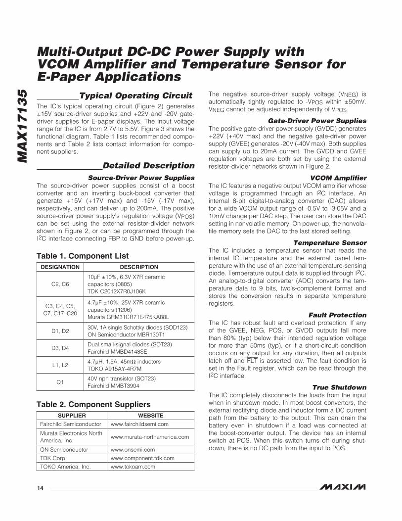
I2C InterfaceThe device supports an I2C-compatible, 2-wire digital interface. SDA is the bidirectional data line and SCL is the clock line of the 2-wire interface corresponding, respectively, to the SDA and SCL lines of the I2C bus. Write to a register by writing the device address byte, a data pointer byte, and a data byte. Read from the IC in one of two ways: if the location latched in the Pointer register is set from the previous read, the new read con-sists of a device address byte, followed by retrieving the corresponding number of data bytes. If the Pointer reg-ister needs to be set to a new address, perform a read operation by writing the device address byte, pointer byte, repeat start, and the device address byte again with the read bit. An inadvertent 8-bit read from a 16-bit register, with the D7 bit low, can cause the device to stop in a state where the SDA line is held low. Ordinarily, this would prevent any further bus communication until the master sends nine additional clock cycles or SDA goes high. At that time, a STOP condition resets the device. If the additional clock cycles are not generated by the master, the IC bus resets and unlocks after the bus time-out period has elapsed.
The device uses the read and write protocols shown in Figure 4.
Figure 4. Read/Write Protocols
BYTE READ FROM PRESET POINTER LOCATION
MSB
STARTSLAVEACK STOPd7 d6 d5 d4 d3 d2 d1 d0
LSB MSB LSB
SLAVE ADDRESS DATA BYTE
0 0 1 0 0 0 11
POINTER SET FOLLOWED BY IMMEDIATE BYTE READ
SLAVE ADDRESS POINTER BYTE
STOPd7 d6 d5 d4 d3 d2 d1 d0
MSB LSB
SLAVE ADDRESS DATA BYTE
MSB
STARTSLAVEACK
SLAVEACK0 0 0 p4 p3 p2 p1 p0
LSB MSB LSB
0 0 1 0 0 0 01SLAVEACK
LSB
0 0 1 0 0 0 11REPEATSTART
WORD READ FROM PRESET POINTER LOCATION
SLAVE ADDRESS MOST SIGNIFICANT DATA BYTE LEAST SIGNIFICANT DATA BYTE
MSB LSB MSB LSB
STARTSLAVEACK d7 d6 d5 d4 d3 d2 d1 d00 0 1 0 0 0 11
MSB
MASTERACK STOP
LSB
d7 d6 d5 d4 d3 d2 d1 d0
POINTER SET FOLLOWED BY IMMEDIATE WORD READ
SLAVE ADDRESS POINTER BYTE SLAVE ADDRESS
MSB
STARTMASTER
ACK 0 0 0 p4 p3 p2 p1 p0
LSB MSB LSB
0 0 1 0 0 0 01
MSB
SLAVEACK
LSB
0 0 1 0 0 0 11 d7 d6 d5 d4 d3 d2 d1 d0
MSB LSB
MOST SIGNIFICANT DATA BYTE
STOPd7 d6 d5 d4 d3 d2 d1 d0
MSB LSB
LEAST SIGNIFICANT DATA BYTE
SLAVEACK
REPEATSTART
MASTERACK
BYTE WRITE
SLAVE ADDRESS POINTER BYTE DATA BYTE
MSB LSB MSB LSB
START SLAVEACK
0 0 0 p4 p3 p2 p1 p00 0 1 0 0 0 01
MSBSLAVEACK
LSB
d6 d5 d4 d3 d2 d1 d0d7 STOPSLAVEACK
MA
X1
71
35
Multi-Output DC-DC Power Supply with VCOM Amplifier and Temperature Sensor for E-Paper Applications
16
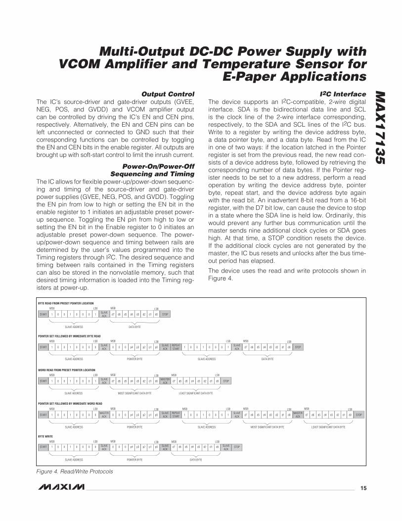
I2C AddressThe IC is a slave-only device and responds to the 7-bit address 90h. The read and write commands can be distin-guished by adding 1 more bit (R/W bit) to the end of the 7-bit slave address, with 1 indicating read, and 0 indicating write.
I2C RegistersThe device contains 20 data registers along with an additional Pointer register. The Pointer register selects which of the other 19 data registers to be read from or written to. At power-up, the Pointer is set to read the External Temperature register at address 0x00. The Pointer register latches the last location to which it was set.
P4–P0 Register Select
A7 A6 A5 A4 A3 A2 A1 A0
1 0 0 1 0 0 0 R-/W
P7 P6 P5 P4 P3 P2 P1 P0
0 0 0 Register Select
P4–P0 (HEX) REGISTER NO. OF BITS POR STATE
00 External Temperature register (read only) (power-up default) 16 N/A
01 Configuration register (read/write) 8 00h
04 Internal Temperature register (read only) 16 N/A
05 Status register (read only) 8 N/A
06 Product Revision register (read only) 8 00h
07 Product ID Register (read only) 8 4Dh
08 DVR register (R/W) 8 FFh
09 Enable register (R/W) 8 00h
0A Fault register (read only) 8 N/A
0B HVINP register (R/W) 8 0Ah
0C Programming Control register (write only) 8 N/A
0Fh Temperature Conversion Rate register 8 04h
10 t1 Timing register (R/W) 8 1Eh (factory default)
11 t2 Timing register (R/W) 8 3Ch (factory default)
12 t3Timing register (R/W) 8 5Ah (factory default)
13 t4 Timing register (R/W) 8 78h (factory default)
14 t5 Timing register (R/W) 8 1Eh (factory default)
15 t6 Timing register (R/W) 8 3Ch (factory default)
16 t7 Timing register (R/W) 8 5Ah (factory default)
17 t8 Timing register (R/W) 8 78h (factory default)
MA
X1
71
35
Multi-Output DC-DC Power Supply with VCOM Amplifier and Temperature Sensor for
E-Paper Applications
17
Configuration Register (01h) (R/W)After the IN and VDD voltages have risen above their respective undervoltage-lockout thresholds, the Shutdown bit (D0) is set to 0 and temperature conver-sions begin immediately. Temperature conversions are continually performed every 1s unless the temperature sensor is put into shutdown mode. Set D0 to 1 to put the temperature sensor in shutdown mode to reduce supply current.
D0: SHUTDOWN: When set to 1, the temperature sensor is shut down.
Status Register (05h), Read OnlyThe Status register indicates whether the IC’s ADC is in the process of performing a temperature conversion and whether there are any fault conditions with the remote temperature-sensing diode. Any fault condition with the external temperature-sensing diode causes the external temperature register to return 7FC0h.
D0: BUSY: Is set to 1 when the ADC is in the process of performing a temperature conversion.
D1: OPEN: Is set to 1 when any connections from DXN and DXP to the temperature-sensing diode are open.
D2: SHORT: Is set to 1 when there is a short-circuit con-dition between DXP and DXN.
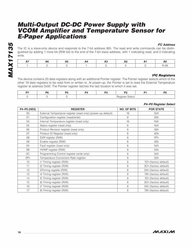
External and Internal Temperature Registers (00h and 04h), Read Only
The temperature data format of the External Temperature register (00h) and the Internal Temperature register (04h) are both 9 bits, two’s complement, and are read
out in word format: an upper byte and a lower byte. Bits D15–D7 contain the temperature data, with the LSB rep-resenting +0.5NC and the MSB representing the sign bit. The last 7 bits of the lower byte, bits D6–D0, are don’t care.
X = Don’t care.
X = Don’t care.
D15 D14 D13 D12 D11 D10 D9 D8 D7 D6 D5 D4 D3 D2 D1 D0
Sign Bit1 = Negative0 = Positive
+64NC +32NC +16NC +8NC +4NC +2NC +1NC +0.5NC X X X X X X X
TEMPERATURE (NC)DIGITAL OUTPUT
BINARY HEX
+125 0111 1101 0XXX XXXX 7D0X
+25 0001 1001 0XXX XXXX 190X
+0.5 0000 0000 1XXX XXXX 008X
0 0000 0000 0XXX XXXX 000X
-0.5 1111 1111 1XXX XXXX FF8X
-25 1110 0111 0XXX XXXX E70X
D7 D6 D5 D4 D3 D2 D1 D0
0 0 0 0 0 0 0 Shutdown
D7 D6 D5 D4 D3 D2 D1 D0
0 0 0 0 0 SHORT OPEN BUSY
MA
X1
71
35
Multi-Output DC-DC Power Supply with VCOM Amplifier and Temperature Sensor for E-Paper Applications
18
Product Revision Register (06h), Read OnlyThis register contains the product revision 0x00h.
Product Identification Register (07h), Read OnlyMaxim is indicated by 0x4Dh.
DVR Register (08h) R/WThe VCOM voltage can be set anywhere between -0.5V and -3.050V with 10mV per LSB by programming the DVR register with a corresponding value as shown in the table below. During power-up, once IN and VDD exceed their undervoltage-lockout thresholds, the DVR register is programmed with a value stored in the nonvolatile memory to set the VCOM voltage. The factory-default DVR value stored in the nonvolatile memory is 7F. See the Programming Control Register (0Ch), Write Only sec-tion for details regarding changing the preset DVR value.
Enable Register (09h) R/WThe output enable functions performed by the EN and CEN pins can also be performed through I2C commands by setting the function’s corresponding enable bit in the Enable register.
Each function’s enable bit is ORed with the status of its corresponding enable pin to determine whether the func-tion is to be performed. If I2C control over the EN and CEN functions is desired, leave the EN and CEN pins unconnected or connect them to GND such that when:
• The EN bit is set to 1; the GVEE, NEG, POS, andGVDD power rails begin a power-up sequence. The sequence order and timing between the startup of each power rail is determined by the information stored in the t1–t4 Timing registers at the time the EN bit is set to 1.
• The EN bit is set to 0; the GVEE, NEG, POS, andGVDD begin a power-down/discharge sequence based on the information stored in the Timing reg-isters. The sequence order and timing between the power-down of each power rail is determined by the information stored in the t5–t8 Timing registers at the time the EN bit is set to 0.
•The CEN bit is set to 1; the VCOM output isenabled.
•TheCENbit is set to 0; theVCOMoutput isdis-charged to ground.
During a fault condition, all bits in the Enable register are cleared (EN = CEN = 0). Driving the EN or CEN pins high or low has no effect on the EN or CEN settings in the Enable register.
D7 D6 D5 D4 D3 D2 D1 D0
0 0 0 0 0 0 0 0
D7 D6 D5 D4 D3 D2 D1 D0
0 1 0 0 1 1 0 1
D7 D6 D5 D4 D3 D2 D1 D0
0 0 0 0 0 0 CEN EN
D7 D6 D5 D4 D3 D2 D1 D0
MSB Bit6 Bit5 Bit4 Bit3 Bit2 Bit1 LSB
DVR REGISTERVCOM OUTPUTVOLTAGE (V)
00h -0.50
01h -0.51
… …
7Fh -1.77
… …
FEh -3.04
FFh -3.05
MA
X1
71
35
Multi-Output DC-DC Power Supply with VCOM Amplifier and Temperature Sensor for
E-Paper Applications
19
Fault Register (0Ah) Read OnlyDuring a fault condition, all outputs of the device are latched off, all bits in the Enable register are set to 0, and the corresponding bit of the fault condition is set in the Fault register (see the table below). After the fault condi-tion is removed, the Fault register is cleared by cycling the VDD supply.
The POK bit in the Fault register is not a fault indicator, but rather a status indicator that is asserted to 1 after FBNG, NEG, POS, and FBPG have all exceeded 80% of their regulation voltages and all soft-start periods have completed. The POK bit is set to 0 once the power-down sequence has been initiated by setting the EN bit to 0 or once a fault condition has occurred. The status of POK itself does not directly affect the status of EN or CEN bits.
Note: The temperature sensor DXN/DXP short-circuit and open-circuit “faults” are not latching faults that cause the IC to shut down and do not set the CEN or EN bits’ status.
FBPG = GVDD undervoltage fault
HVINP = HVINP undervoltage fault
HVINN = HVINN undervoltage fault
FBNG = GVEE undervoltage fault
HVINPSC = HVINP short-circuit fault
HVINNSC = HVINN short-circuit fault
OT = Thermal shutdown
POK = Power-OK
HVINP Register (0Bh) R/WThe POS regulation voltage is determined by the boost converter’s output regulation voltage (VHVINP). The HVINP regulation voltage is set by using a resistor-divider network or by programming the corresponding value of
the desired HVINP regulation voltage into the HVINP reg-ister through I2C (see the table below). Programming the HVINP register to set the HVINP regulation voltage gives the flexibility to change the HVINP regulation voltage between each power-up sequence of the GVEE, NEG, POS, and GVDD rails and removes external components.
To set the HVINP regulation voltage through I2C, connect the FBP pin to GND. With FBP connected to GND, the HVINP register is automatically loaded with 0Ah and the HVINP regulation voltage is set to +15V after IN and VDD have exceeded their undervoltage-lockout thresholds. If another HVINP regulation voltage other than +15V is desired, write a new value to the HVINP register that cor-responds to the desired HVINP regulation voltage after IN and VDD have exceeded their undervoltage-lockout thresholds, but before EN is asserted high. The new HVINP regulation voltage is maintained until a new value is written to the HVINP register or the VDD input power is cycled. After cycling VDD, the HVINP register is again reloaded with 0Ah such that it is necessary to rewrite the HVINP register to change the HVINP regulation voltage to another voltage other than VHVINP = 15V.
The HVINP register can be programmed to provide a POS regulation voltage from 00h (VPOS = 5V) to 0Ch (VPOS = 17V) adjustable in 1V steps.
D7 D6 D5 D4 D3 D2 D1 D0
POK OT HVINNSC HVINPSC FBNG HVINN HVINP FBPG
D7 D6 D5 D4 D3 D2 D1 D0
0 0 0 0 MSB Bit2 Bit1 LSB
HVINP REGISTERHVINP OUTPUTVOLTAGE (V)
00h 5
01h 6
... ...
0Ah 15
0Bh 16
0Ch 17
MA
X1
71
35
Multi-Output DC-DC Power Supply with VCOM Amplifier and Temperature Sensor for E-Paper Applications
20
Conversion Rate Control Byte (0Fh) R/WThe Conversion Rate register (0Fh) programs the time interval between conversions in the free-running auto-convert mode of the temperature sensors. This variable-rate control reduces the supply current in portable-equipment applications. The conversion rate control byte’s POR state is 04h. The control mechanism looks only at the 3 LSBs of this register, so the upper 5 bits are “don’t care” bits, which should be set to zero. The conversion rate tolerance is ±25% at any rate setting.
Valid A/D conversion results are available one total con-version time after the initiating conversion, whether the conversion is initiated through the Shutdown bit in the Configuration Register or initial power-up. Changing the conversion rate can also affect the delay until new results are available.
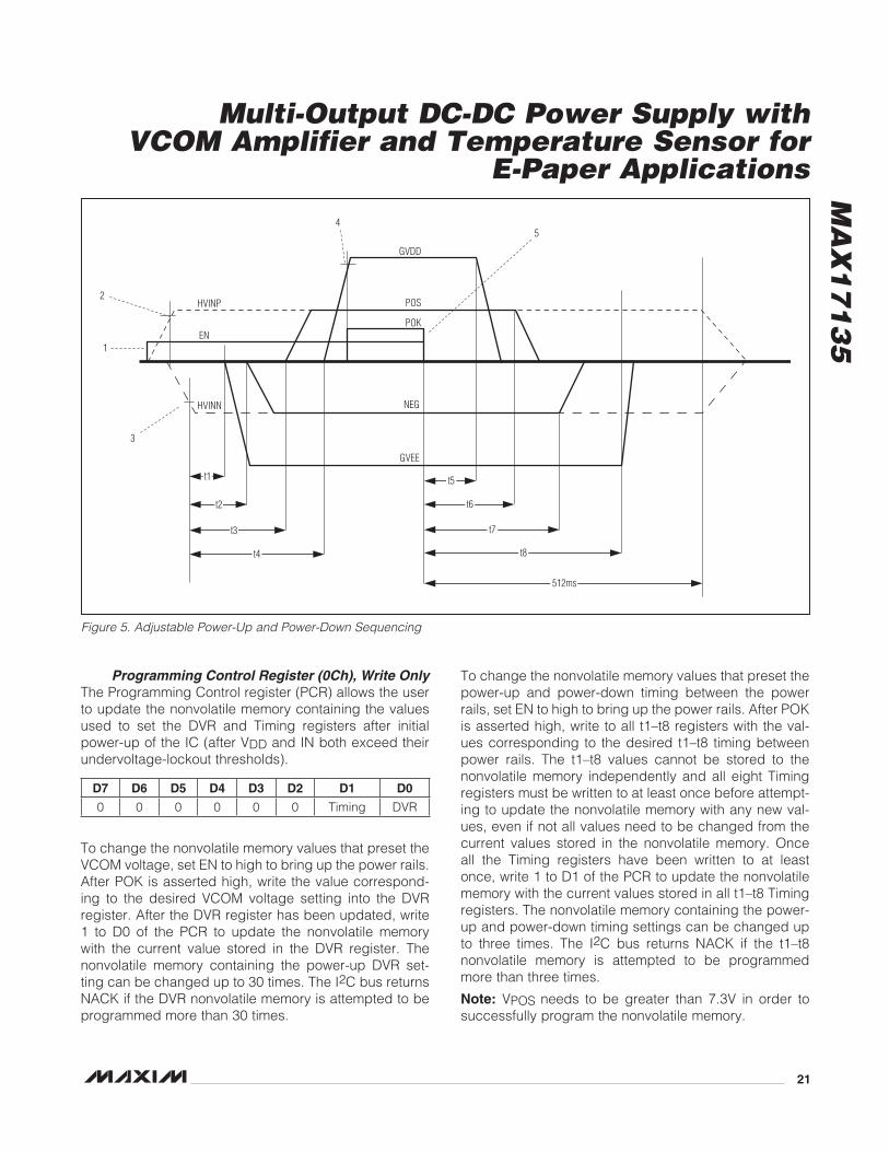
t1–t8 Timing Registers (10h–17h) R/WFigure 5 shows the start-up and shutdown sequence of the power rails:
• TheHVINPpower railbegins itssoft-startsequenceonce EN is driven high or the EN bit in the Enable register is set to 1.
• TheHVINNpowerrailbegins itssoft-startsequenceonce the HVINP soft-start period has expired.
• TheGVEE,NEG, POS, andGVDDpower rails startup t1–t4ms after the expiration of the HVINN soft-start period.
• POK is asserted high after FBNG, NEG, POS, andFBPG have all exceeded 80% of their regulation volt-ages and all the corresponding power rails’ soft-start periods have expired.
• Once EN is driven low or the EN bit in the Enableregister is set to 0 (while the EN is disconnected or is connected to GND), POK is asserted low and each power rail is discharged at a time depending on the values stored in the timing registers (t5–t8). Approximately 512ms after EN is driven low, HVINP and HVINN are powered down but not discharged.
The power-up/power-down sequence and timing between the GVEE, NEG, POS, and GVDD power rails can be set by programming the t1–t8 registers with cor-responding values according to the table below.
The binary value stored in a register directly corresponds to the time in ms.
During power-up of the device, once IN and VDD exceed their undervoltage-lockout thresholds, the t1–t8 registers are loaded with values stored in the nonvolatile memory to preset the t1–t8 timing. The factory-default timing set-tings in the nonvolatile memory are:
• t1=t5=30ms
• t2=t6=60ms
• t3=t7=90ms
• t4=t8=120ms
To change the preset t1–t8 timing, see the Programming Control Register (0Ch), Write Only section.
D7 D6 D5 D4 D3 D2 D1 D0
128ms 64ms 32ms 16ms 8ms 4ms 2ms 1ms
VALUE STORED IN A TIMING REGISTER (t1–t8)
TIME (ms)
00h 0
01h 1
... ...
FEh 254
FFh 255
DATACONVERSION
RATE (Hz)
AVERAGE SUPPLY CURRENT OF TEMP-SENSOR BLOCK (μA)
00h 0.0625 14
01h 0.125 18
02h 0.25 26
03h 0.5 41
04h 1 72
05h 2 133
06h 4 255
07h 8 500
08h to FFhDepends on the
3 LSBDepends on the 3 LSB
MA
X1
71
35
Multi-Output DC-DC Power Supply with VCOM Amplifier and Temperature Sensor for
E-Paper Applications
21
Figure 5. Adjustable Power-Up and Power-Down Sequencing
Programming Control Register (0Ch), Write OnlyThe Programming Control register (PCR) allows the user to update the nonvolatile memory containing the values used to set the DVR and Timing registers after initial power-up of the IC (after VDD and IN both exceed their undervoltage-lockout thresholds).
To change the nonvolatile memory values that preset the VCOM voltage, set EN to high to bring up the power rails. After POK is asserted high, write the value correspond-ing to the desired VCOM voltage setting into the DVR register. After the DVR register has been updated, write 1 to D0 of the PCR to update the nonvolatile memory with the current value stored in the DVR register. The nonvolatile memory containing the power-up DVR set-ting can be changed up to 30 times. The I2C bus returns NACK if the DVR nonvolatile memory is attempted to be programmed more than 30 times.
To change the nonvolatile memory values that preset the power-up and power-down timing between the power rails, set EN to high to bring up the power rails. After POK is asserted high, write to all t1–t8 registers with the val-ues corresponding to the desired t1–t8 timing between power rails. The t1–t8 values cannot be stored to the nonvolatile memory independently and all eight Timing registers must be written to at least once before attempt-ing to update the nonvolatile memory with any new val-ues, even if not all values need to be changed from the current values stored in the nonvolatile memory. Once all the Timing registers have been written to at least once, write 1 to D1 of the PCR to update the nonvolatile memory with the current values stored in all t1–t8 Timing registers. The nonvolatile memory containing the power-up and power-down timing settings can be changed up to three times. The I2C bus returns NACK if the t1–t8 nonvolatile memory is attempted to be programmed more than three times.
Note: VPOS needs to be greater than 7.3V in order to successfully program the nonvolatile memory.
HVINP2
1
3
45
GVDD
POS
POK
NEG
GVEE
EN
HVINN
t1 t5
t6
t7
t8
t2
t3
t4
512ms
D7 D6 D5 D4 D3 D2 D1 D0
0 0 0 0 0 0 Timing DVR
MA
X1
71
35
Multi-Output DC-DC Power Supply with VCOM Amplifier and Temperature Sensor for E-Paper Applications
22
PCB Layout and GroundingCareful PCB layout is important for proper operation. Use the following guidelines for good PCB layout:
• Minimize the inner loop area created by the boostconverter high-switching current connections. Place D1 and C3 close to the IC such that the traces con-necting the LXP pin to the anode of D1, the cathode of D1 to C3, and C3 to the PGND pin are kept as short as possible to minimize the loop area contained within these connections. Make these connections with short, wide traces.
• Minimize the inner loop area created by the buck-boost converter high-switching current connections. Place C6, C7, and D2 close to the IC such that the traces connecting C6 to the INN pin, the LXN pin to the cathode of D2, the anode of D2 to C7, and C6 ground connection to C7 are kept as short as pos-sible to minimize the loop area contained within these connections. Make these connections with short, wide traces.
• Avoid using vias in the high-current paths. If viasare unavoidable, use many vias in parallel to reduce resistance and inductance.
• Create apowerground island (PGND) consisting ofthe PGND pin, the input and output capacitor ground connections, the charge-pump capacitor ground con-nections, and the buck-boost inductor ground connec-tion. Connect all these together with short, wide traces or a small ground plane. Maximizing the width of the power ground traces improves efficiency and reduces output-voltage ripple and noise spikes. Create an ana-log ground plane (GND) consisting of the GND pin, all the feedback-divider ground connections, the IN, VDD, and REF bypass capacitor ground connections, and the device’s exposed backside paddle.
• Connect the GND and PGND islands by connect-ing the PGND pin directly to the exposed backside paddle. Make no other connections between these separate ground planes.
• Placethefeedback-voltage-dividerresistorsascloseas possible to their respective feedback pins. Keep the traces connecting the feedback resistors to their respective feedback pins as short as possible. Placing the resistors far away causes the feedback trace to become an antenna that can pick up switch-ing noise. Care should be taken to avoid running any feedback trace near the LXP, LXN, DP, or DN switch-ing nodes.
• Place the IN, VDD, and REF bypass capacitors as close as possible to the IC. The ground connections of the IN, VDD, and REF bypass capacitors should be connected directly to the analog ground plane or directly to the GND pin with a wide trace.
• Minimize the length and maximize the width of thetraces between the output capacitors and the load for best transient responses.
• KeepsensitivesignalsawayfromtheLXP,LXN,DP,and DN switching nodes. Use DC traces as a shield if necessary.
Refer to the MAX17135 evaluation kit for an example of proper board layout.
Chip InformationPROCESS: BiCMOS
Package InformationFor the latest package outline information and land pat terns (footprints), go to www.maxim-ic.com/packages. Note that a “+”, “#”, or “-” in the package code indicates RoHS status only. Package drawings may show a different suf fix character, but the drawing pertains to the package regardless of RoHS status.
PACKAGE TYPE
PACKAGE CODE
OUTLINE NO.
LAND PATTERN
NO.
32 TQFN-EP T3255N+1 21-0140 90-0015
MA
X1
71
35
Multi-Output DC-DC Power Supply with VCOM Amplifier and Temperature Sensor for
E-Paper Applications
Maxim cannot assume responsibility for use of any circuitry other than circuitry entirely embodied in a Maxim product. No circuit patent licenses are implied. Maxim reserves the right to change the circuitry and specifications without notice at any time. The parametric values (min and max limits) shown in the Electrical Characteristics table are guaranteed. Other parametric values quoted in this data sheet are provided for guidance.
Maxim Integrated Products, 120 San Gabriel Drive, Sunnyvale, CA 94086 408-737-7600 23
© 2012 Maxim Integrated Products Maxim is a registered trademark of Maxim Integrated Products, Inc.
Revision HistoryREVISIONNUMBER
REVISIONDATE
DESCRIPTIONPAGES
CHANGED
0 7/11 Initial release —
1 12/11 Typical Operating Circuit values updated 12
2 5/12 Inverting Regulator section in EC table changed to meet QA standard 3