Embed Size (px)
DESCRIPTION
Exam 2 Review Two’s Complement Arithmetic Ripple carry ALU logic and performance Look-ahead techniques Basic multiplication and division ( non-restoring) algorithms IEEE 754 floating point standard (definition provided) - PowerPoint PPT Presentation
Citation preview
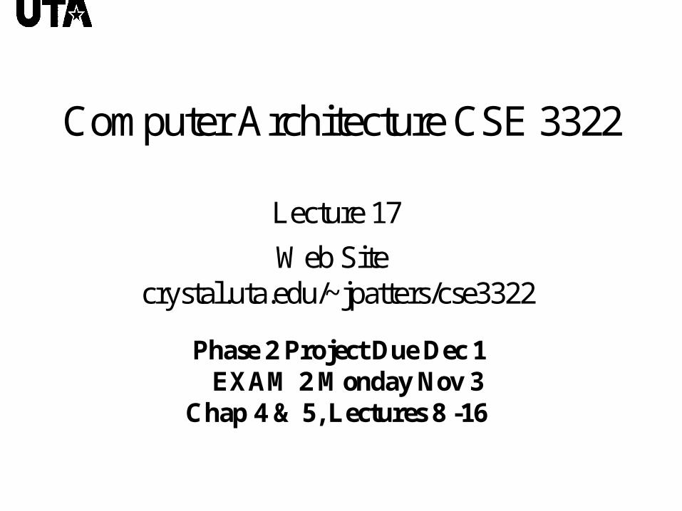
Computer Architecture CSE 3322
Lecture 17
Web Sitecrystal.uta.edu/~jpatters/cse3322
Phase 2 Project Due Dec 1EXAM 2 Monday Nov 3
Chap 4 & 5, Lectures 8 -16
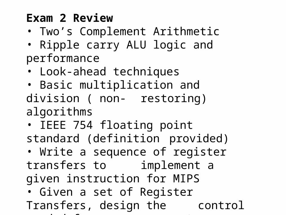
Exam 2 Review• Two’s Complement Arithmetic• Ripple carry ALU logic and performance• Look-ahead techniques• Basic multiplication and division ( non-restoring) algorithms• IEEE 754 floating point standard (definition
provided)• Write a sequence of register transfers to implement a given instruction for MIPS• Given a set of Register Transfers, design the
control needed for some component

S0 M[PC] IR, PC + 4 PC, S1 SS1 R[IR[25-21]] A, R[IR[20-16]] B, PC + shlt2[sign_ext(IR[15-0])] ALUOut, (‘LW’+’SW’)S2 + ‘R’S6 + ‘BEQ’S8 + ‘J’S9 SS2 A + sign_ext(IR[15-0]) ALUOut,
‘LW’S3 + ‘SW’S5 SS3 M[ ALUOut] MDR, S4 SS4 MDR R[ IR[20-16]], S0 SS5 B M[ ALUOut], S0 SS6 A op B ALUOut, S7 SS7 ALUOut R[IR[15-11]], S0 SS8 Zero PC + Zero ALUOut PC, S0 SS9 PC[31-28] : shlt2(IR[25-0]) PC, S0 S
State Register Transfers
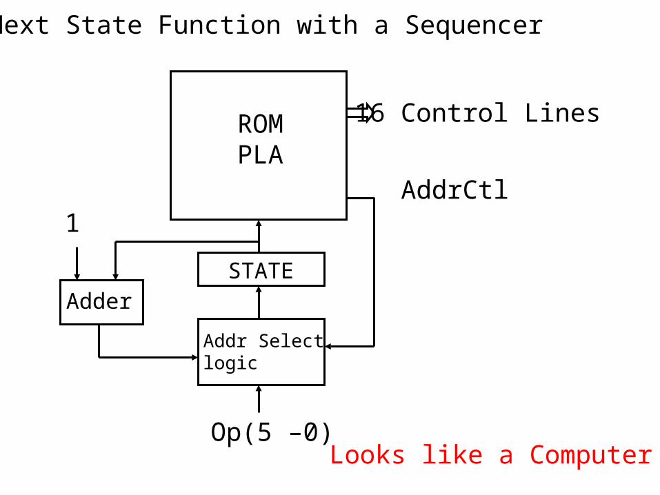
Next State Function with a Sequencer
16 Control LinesROMPLA
STATE
Adder
1
Addr Selectlogic
Op(5 –0)
AddrCtl
Looks like a Computer !
Microprogramming
• Define a symbolic set of microinstructions used to implement each instruction
Microprogramming
• Define a symbolic set of microinstructions used to implement each instruction
• The microassembler will check for inconsistencies and convert to binary code
Microprogramming
• Define a symbolic set of microinstructions used to implement each instruction
• The microassembler will check for inconsistencies and convert to binary code
• Define independent fields to determine datapath control signals that must be asserted

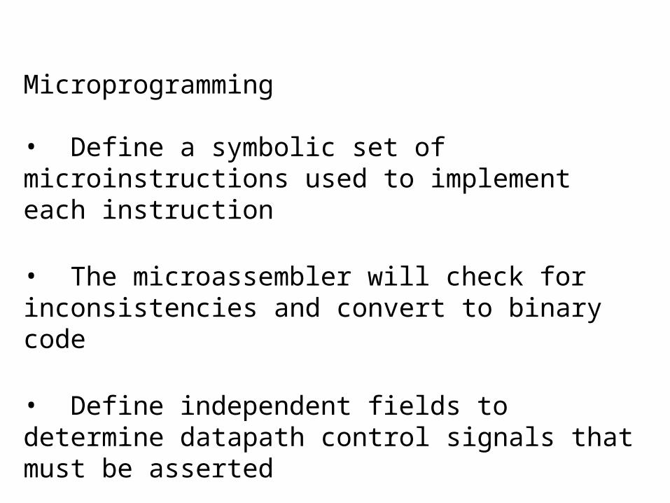
Microprogramming
• Define a symbolic set of microinstructions used to implement each instruction
• The microassembler will check for inconsistencies and convert to binary code
• Define independent fields to determine datapath control signals that must be asserted
• Define a field to determine the next state
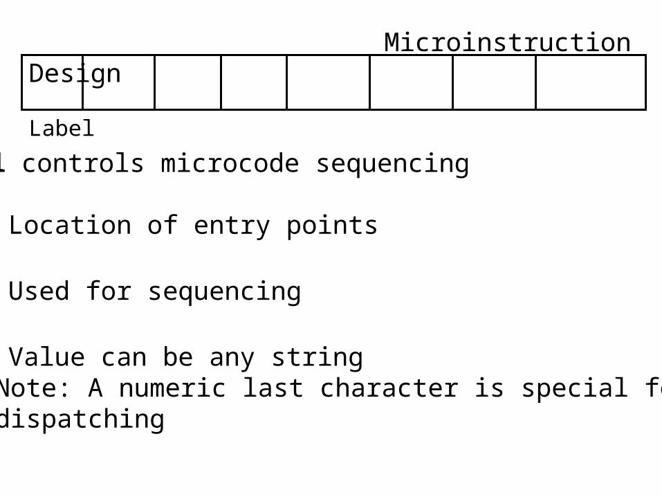
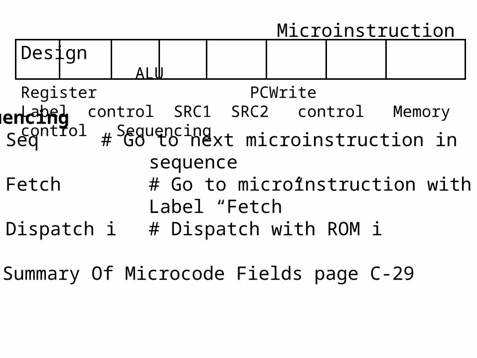
Microinstruction Design Label
Label controls microcode sequencing
• Location of entry points
• Used for sequencing
• Value can be any stringNote: A numeric last character is special fordispatching
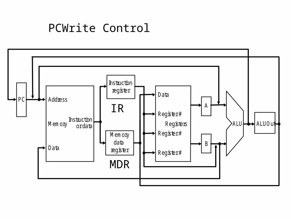
PC
Memory
Address
Instructionor data
Data
Instructionregister
Registers
Register #
Data
Register #
Register #
ALU
Memorydata
register
A
B
ALUOut
IR
MDR
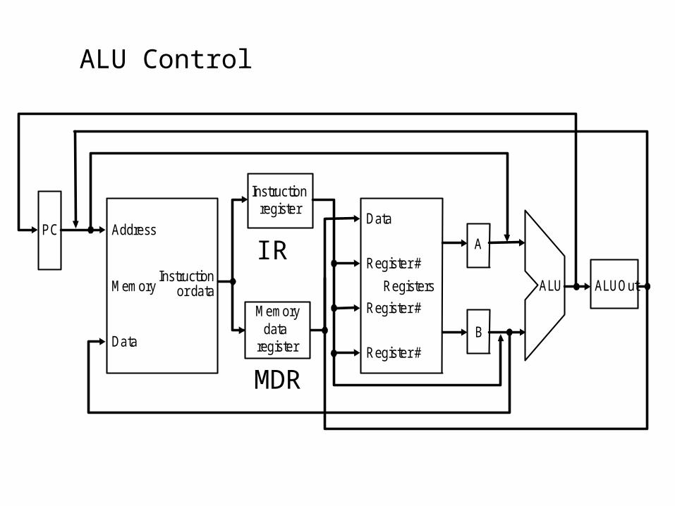
ALU Control
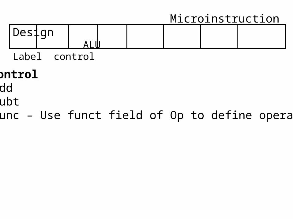
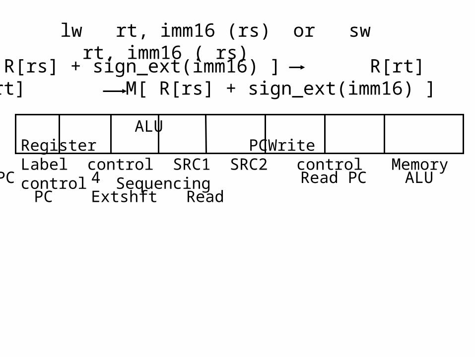
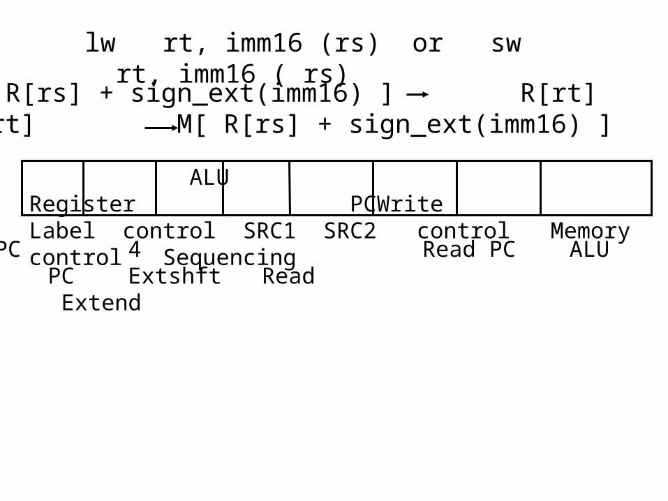
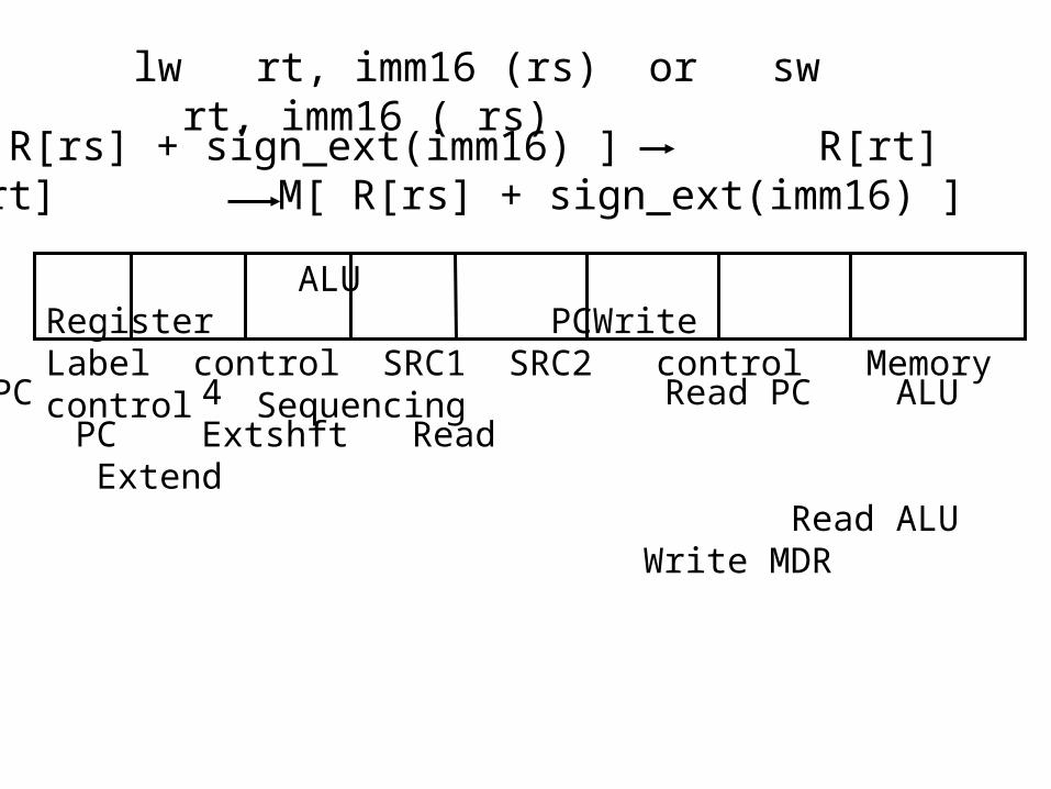
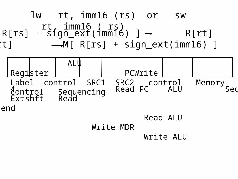
Microinstruction Design ALULabel control
ALU controlAddSubtFunc – Use funct field of Op to define operation
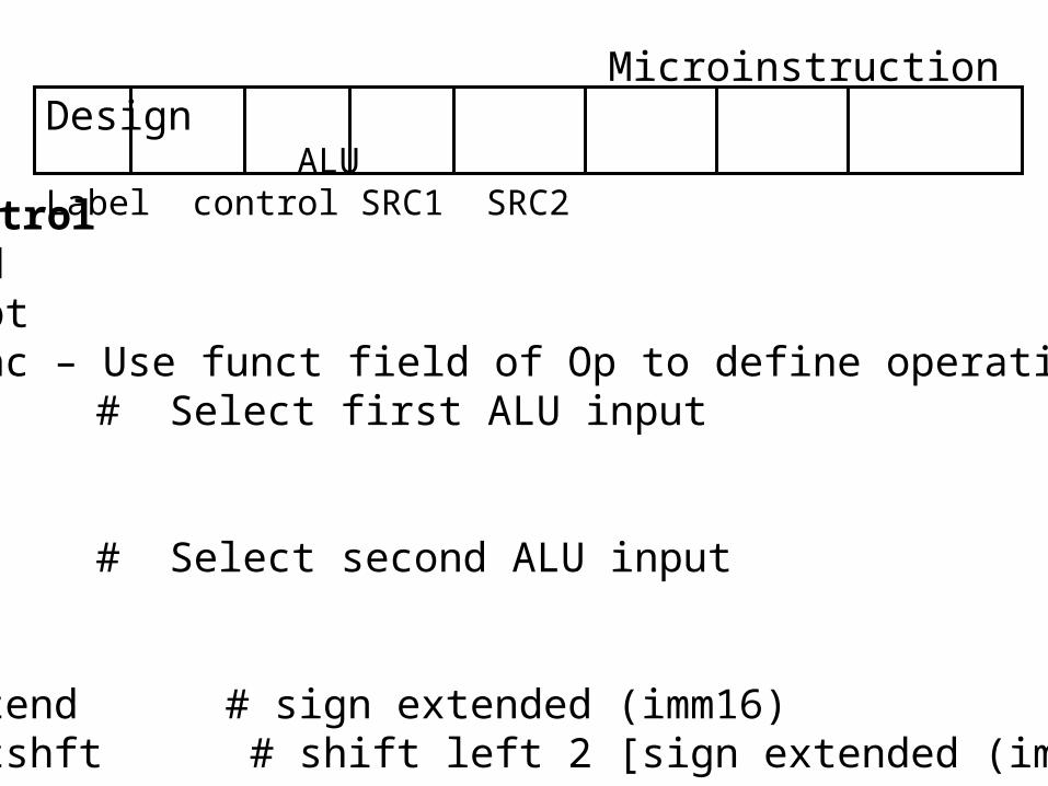
Microinstruction Design ALULabel control SRC1 SRC2
ALU controlAddSubtFunc – Use funct field of Op to define operation
SRC1 # Select first ALU inputPCA
SRC2 # Select second ALU inputB4Extend # sign extended (imm16)Extshft # shift left 2 [sign extended (imm16)]
PC
Memory
Address
Instructionor data
Data
Instructionregister
Registers
Register #
Data
Register #
Register #
ALU
Memorydata
register
A
B
ALUOut
IR
MDR
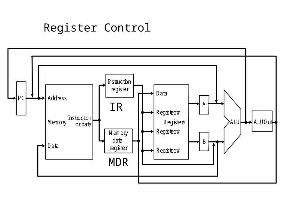
Register Control
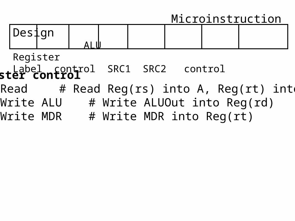
Microinstruction Design ALU RegisterLabel control SRC1 SRC2 control
Register controlRead # Read Reg(rs) into A, Reg(rt) into BWrite ALU # Write ALUOut into Reg(rd)Write MDR # Write MDR into Reg(rt)
PC
Memory
Address
Instructionor data
Data
Instructionregister
Registers
Register #
Data
Register #
Register #
ALU
Memorydata
register
A
B
ALUOut
IR
MDR
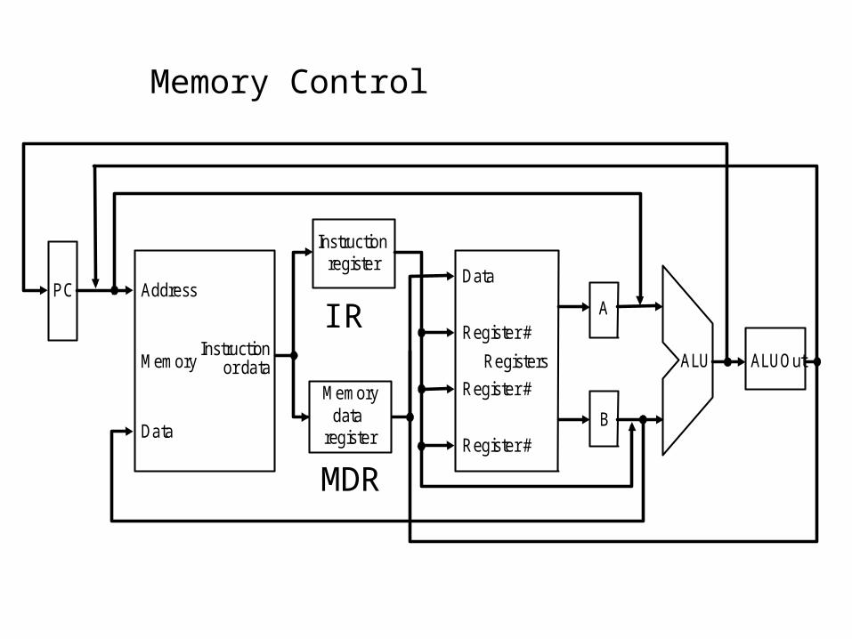
Memory Control
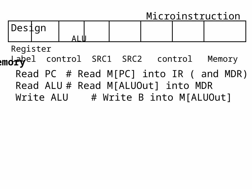
Microinstruction Design ALU Register Label control SRC1 SRC2 control Memory
MemoryRead PC # Read M[PC] into IR ( and MDR)Read ALU # Read M[ALUOut] into MDRWrite ALU # Write B into M[ALUOut]
PC
Memory
Address
Instructionor data
Data
Instructionregister
Registers
Register #
Data
Register #
Register #
ALU
Memorydata
register
A
B
ALUOut
IR
MDR
PCWrite Control
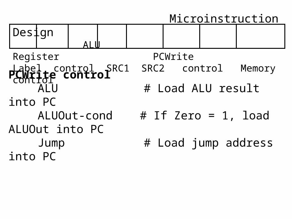
Microinstruction Design ALU Register PCWriteLabel control SRC1 SRC2 control Memory control
PCWrite controlALU # Load ALU result into PCALUOut-cond # If Zero = 1, load ALUOut into PCJump # Load jump address into PC
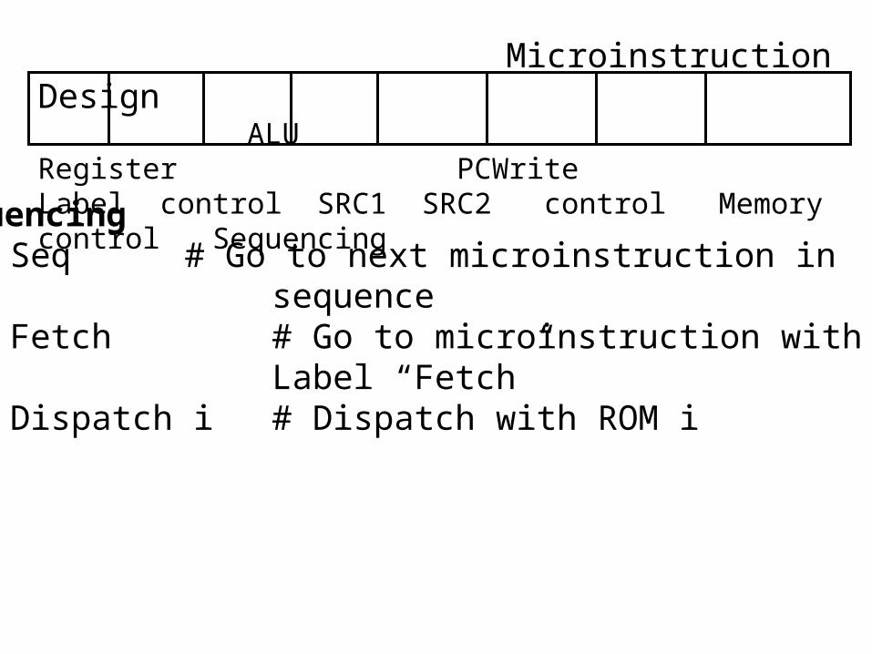
Microinstruction Design ALU Register PCWriteLabel control SRC1 SRC2 control Memory control Sequencing
SequencingSeq # Go to next microinstruction in
sequenceFetch # Go to microinstruction with
Label “Fetch”Dispatch i # Dispatch with ROM i
Microinstruction Design ALU Register PCWriteLabel control SRC1 SRC2 control Memory control Sequencing
SequencingSeq # Go to next microinstruction in
sequenceFetch # Go to microinstruction with
Label “Fetch”Dispatch i # Dispatch with ROM i
See Summary Of Microcode Fields page C-29
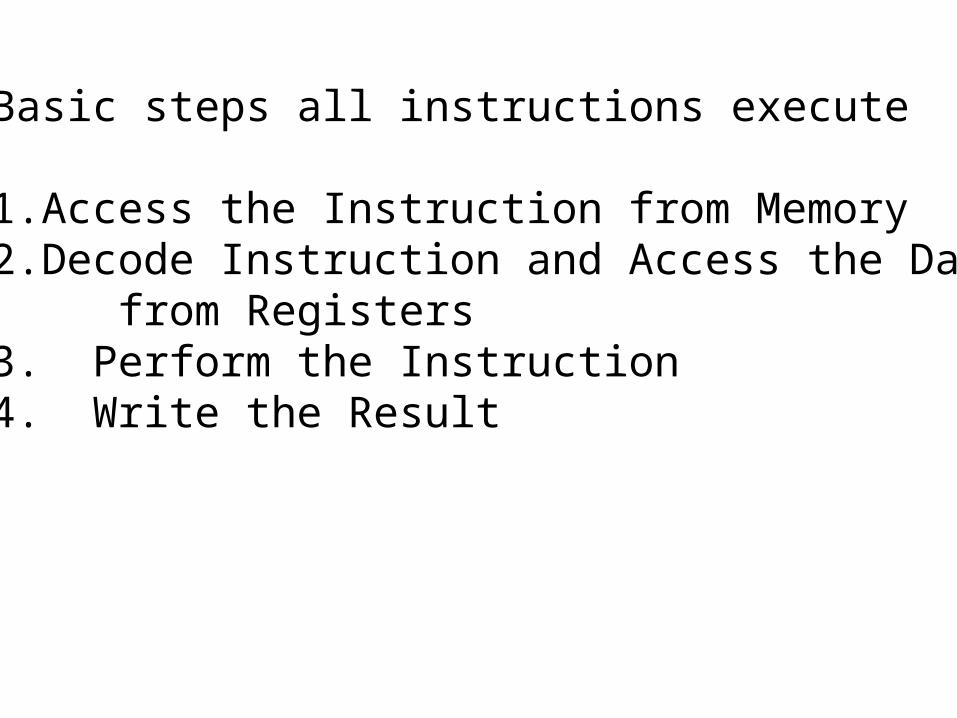
Basic steps all instructions execute
1. Access the Instruction from Memory2. Decode Instruction and Access the Data from Registers 3. Perform the Instruction4. Write the Result
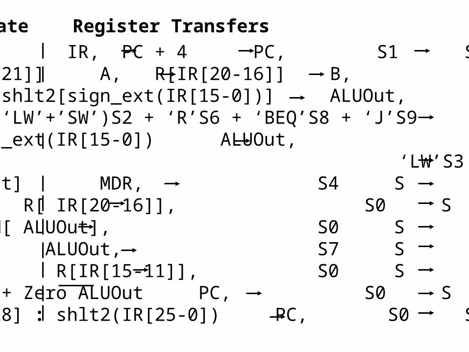
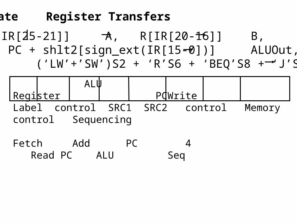
S0 M[PC] IR, PC + 4 PC, S1 SS1 R[IR[25-21]] A, R[IR[20-16]] B, PC + shlt2[sign_ext(IR[15-0])] ALUOut, (‘LW’+’SW’)S2 + ‘R’S6 + ‘BEQ’S8 + ‘J’S9 SS2 A + sign_ext(IR[15-0]) ALUOut,
‘LW’S3 + ‘SW’S5 SS3 M[ ALUOut] MDR, S4 SS4 MDR R[ IR[20-16]], S0 SS5 B M[ ALUOut], S0 SS6 A op B ALUOut, S7 SS7 ALUOut R[IR[15-11]], S0 SS8 Zero PC + Zero ALUOut PC, S0 SS9 PC[31-28] : shlt2(IR[25-0]) PC, S0 S
State Register Transfers
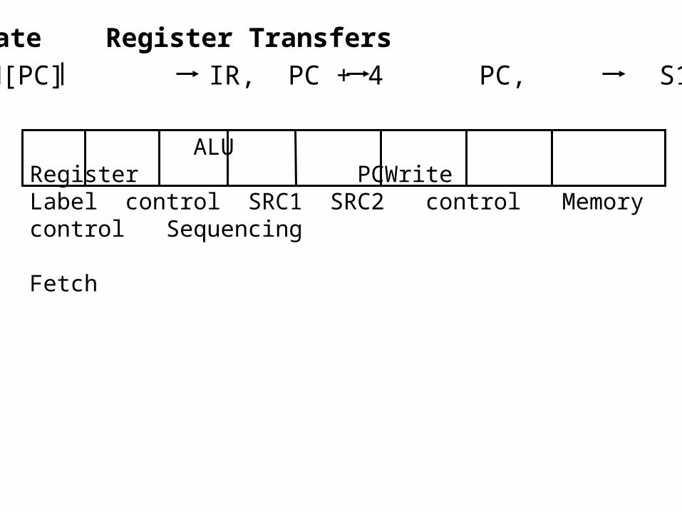
S0 M[PC] IR, PC + 4 PC, S1 S
State Register Transfers
ALU Register PCWriteLabel control SRC1 SRC2 control Memory control Sequencing
Fetch
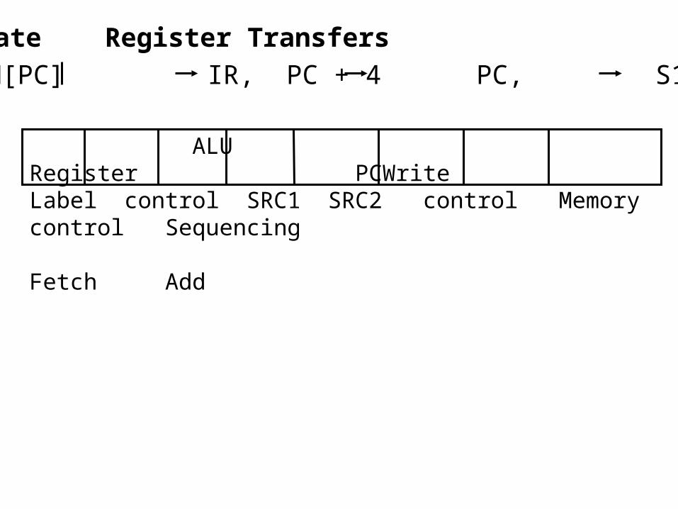
S0 M[PC] IR, PC + 4 PC, S1 S
State Register Transfers
ALU Register PCWriteLabel control SRC1 SRC2 control Memory control Sequencing
Fetch Add

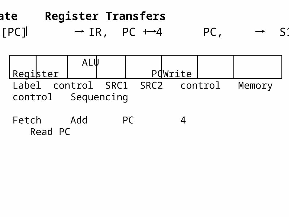
S0 M[PC] IR, PC + 4 PC, S1 S
State Register Transfers
ALU Register PCWriteLabel control SRC1 SRC2 control Memory control Sequencing
Fetch Add PC 4
S0 M[PC] IR, PC + 4 PC, S1 S
State Register Transfers
ALU Register PCWriteLabel control SRC1 SRC2 control Memory control Sequencing
Fetch Add PC 4 Read PC
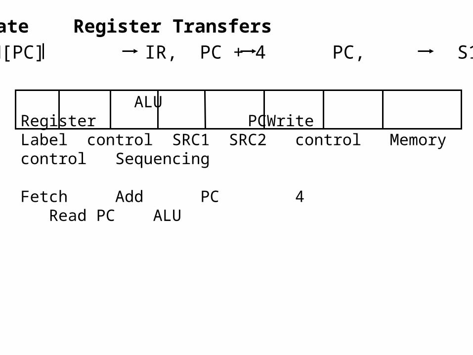
S0 M[PC] IR, PC + 4 PC, S1 S
State Register Transfers
ALU Register PCWriteLabel control SRC1 SRC2 control Memory control Sequencing
Fetch Add PC 4 Read PC ALU
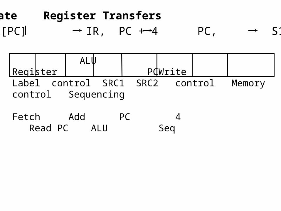
S0 M[PC] IR, PC + 4 PC, S1 S
State Register Transfers
ALU Register PCWriteLabel control SRC1 SRC2 control Memory control Sequencing
Fetch Add PC 4 Read PC ALU Seq
State Register Transfers
ALU Register PCWriteLabel control SRC1 SRC2 control Memory control Sequencing
Fetch Add PC 4 Read PC ALU Seq
S1 R[IR[25-21]] A, R[IR[20-16]] B, PC + shlt2[sign_ext(IR[15-0])] ALUOut, (‘LW’+’SW’)S2 + ‘R’S6 + ‘BEQ’S8 + ‘J’S9 S
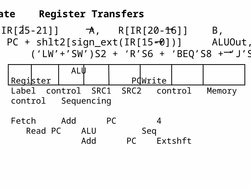
State Register Transfers
ALU Register PCWriteLabel control SRC1 SRC2 control Memory control Sequencing
Fetch Add PC 4 Read PC ALU Seq Add PC Extshft
S1 R[IR[25-21]] A, R[IR[20-16]] B, PC + shlt2[sign_ext(IR[15-0])] ALUOut, (‘LW’+’SW’)S2 + ‘R’S6 + ‘BEQ’S8 + ‘J’S9 S
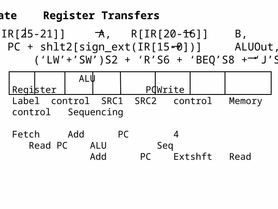
State Register Transfers
ALU Register PCWriteLabel control SRC1 SRC2 control Memory control Sequencing
Fetch Add PC 4 Read PC ALU Seq Add PC Extshft Read
S1 R[IR[25-21]] A, R[IR[20-16]] B, PC + shlt2[sign_ext(IR[15-0])] ALUOut, (‘LW’+’SW’)S2 + ‘R’S6 + ‘BEQ’S8 + ‘J’S9 S
State Register Transfers
ALU Register PCWriteLabel control SRC1 SRC2 control Memory control Sequencing
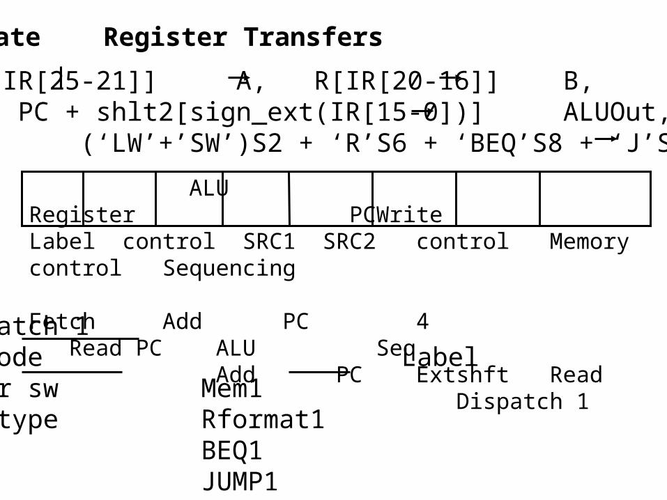
Fetch Add PC 4 Read PC ALU Seq Add PC Extshft Read Dispatch 1
S1 R[IR[25-21]] A, R[IR[20-16]] B, PC + shlt2[sign_ext(IR[15-0])] ALUOut, (‘LW’+’SW’)S2 + ‘R’S6 + ‘BEQ’S8 + ‘J’S9 S
Dispatch 1 Op Code Labellw or sw Mem1R – type Rformat1beq BEQ1j JUMP1
ALU Register PCWriteLabel control SRC1 SRC2 control Memory control Sequencing
lw rt, imm16 (rs) or sw rt, imm16 ( rs)
M[ R[rs] + sign_ext(imm16) ] R[rt]R[rt] M[ R[rs] + sign_ext(imm16) ]
Fetch Add PC 4 Read PC ALU Seq Add PC Extshft Read Dispatch 1Mem1
ALU Register PCWriteLabel control SRC1 SRC2 control Memory control Sequencing
lw rt, imm16 (rs) or sw rt, imm16 ( rs)
M[ R[rs] + sign_ext(imm16) ] R[rt]R[rt] M[ R[rs] + sign_ext(imm16) ]
Fetch Add PC 4 Read PC ALU Seq Add PC Extshft Read Dispatch 1Mem1 Add A Extend Dispatch 2
ALU Register PCWriteLabel control SRC1 SRC2 control Memory control Sequencing
lw rt, imm16 (rs) or sw rt, imm16 ( rs)
M[ R[rs] + sign_ext(imm16) ] R[rt]R[rt] M[ R[rs] + sign_ext(imm16) ]
Fetch Add PC 4 Read PC ALU Seq Add PC Extshft Read Dispatch 1Mem1 Add A Extend Dispatch 2LW2 Read ALU Seq Write MDR Fetch
ALU Register PCWriteLabel control SRC1 SRC2 control Memory control Sequencing
lw rt, imm16 (rs) or sw rt, imm16 ( rs)
M[ R[rs] + sign_ext(imm16) ] R[rt]R[rt] M[ R[rs] + sign_ext(imm16) ]
Fetch Add PC 4 Read PC ALU Seq Add PC Extshft Read Dispatch 1Mem1 Add A Extend Dispatch 2LW2 Read ALU Seq Write MDR FetchSW2 Write ALU Fetch
ALU Register PCWriteLabel control SRC1 SRC2 control Memory control Sequencing
Fetch Add PC 4 Read PC ALU Seq Add PC Extshft Read Dispatch 1Rfmat1
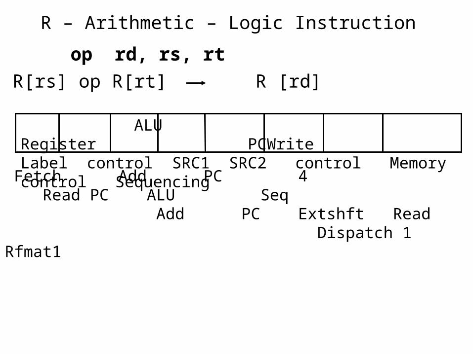
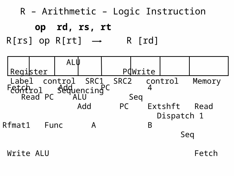
op rd, rs, rt
R – Arithmetic – Logic Instruction
R[rs] op R[rt] R [rd]
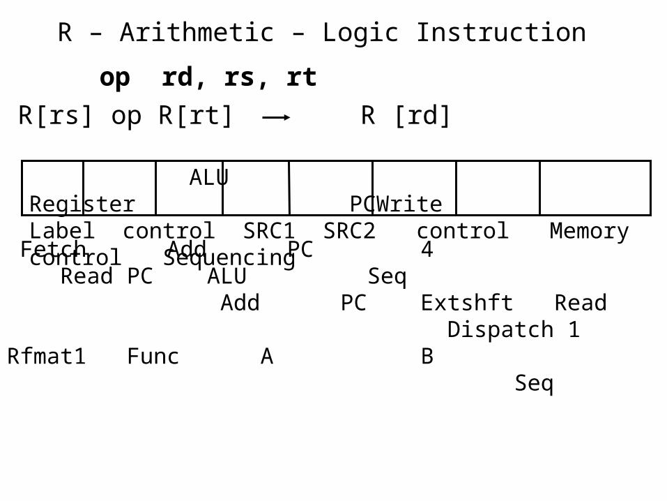
ALU Register PCWriteLabel control SRC1 SRC2 control Memory control Sequencing
Fetch Add PC 4 Read PC ALU Seq Add PC Extshft Read Dispatch 1Rfmat1 Func A B Seq
op rd, rs, rt
R – Arithmetic – Logic Instruction
R[rs] op R[rt] R [rd]
ALU Register PCWriteLabel control SRC1 SRC2 control Memory control Sequencing
Fetch Add PC 4 Read PC ALU Seq Add PC Extshft Read Dispatch 1Rfmat1 Func A B Seq Write ALU Fetch
op rd, rs, rt
R – Arithmetic – Logic Instruction
R[rs] op R[rt] R [rd]
ALU Register PCWriteLabel control SRC1 SRC2 control Memory control Sequencing
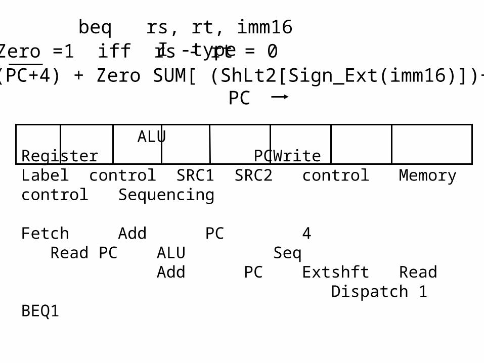
Fetch Add PC 4 Read PC ALU Seq Add PC Extshft Read Dispatch 1BEQ1
beq rs, rt, imm16 I -type
Zero (PC+4) + Zero SUM[ (ShLt2[Sign_Ext(imm16)])+PC+4]PC
Zero =1 iff rs - rt = 0
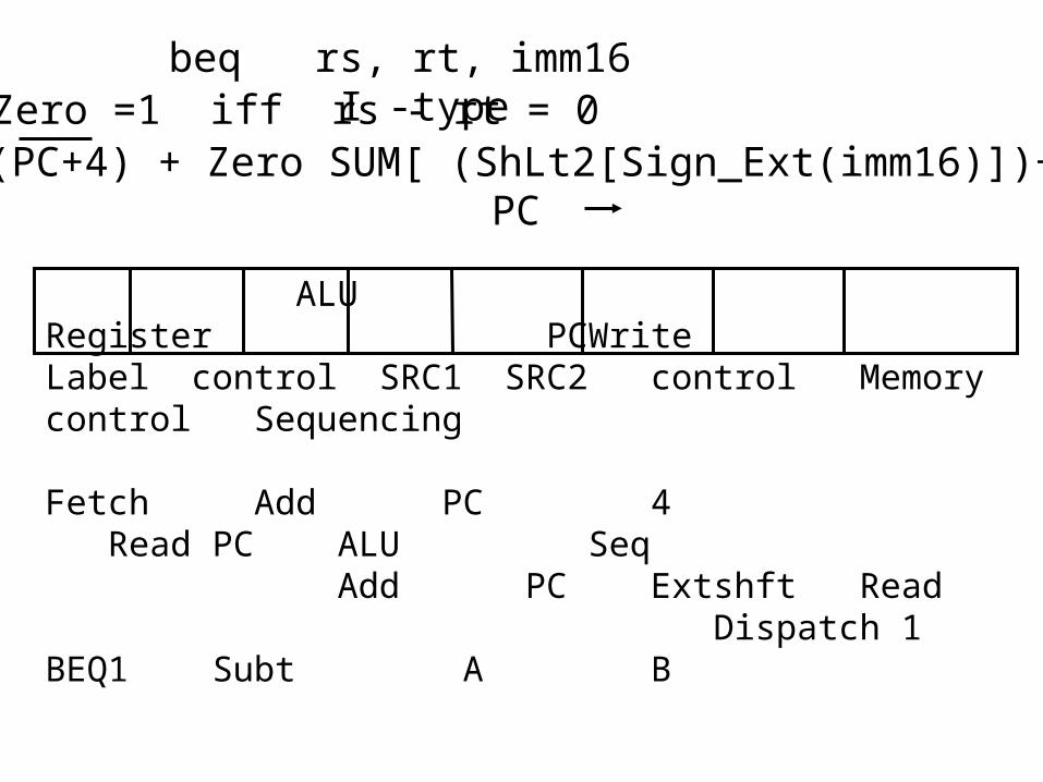
ALU Register PCWriteLabel control SRC1 SRC2 control Memory control Sequencing
Fetch Add PC 4 Read PC ALU Seq Add PC Extshft Read Dispatch 1BEQ1 Subt A B
beq rs, rt, imm16 I -type
Zero (PC+4) + Zero SUM[ (ShLt2[Sign_Ext(imm16)])+PC+4]PC
Zero =1 iff rs - rt = 0
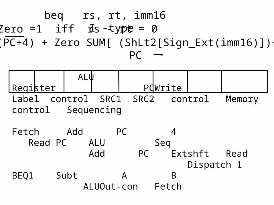
ALU Register PCWriteLabel control SRC1 SRC2 control Memory control Sequencing
Fetch Add PC 4 Read PC ALU Seq Add PC Extshft Read Dispatch 1BEQ1 Subt A B ALUOut-con Fetch
beq rs, rt, imm16 I -type
Zero (PC+4) + Zero SUM[ (ShLt2[Sign_Ext(imm16)])+PC+4]PC
Zero =1 iff rs - rt = 0
ALU Register PCWriteLabel control SRC1 SRC2 control Memory control Sequencing
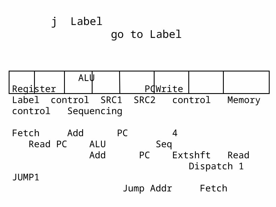
Fetch Add PC 4 Read PC ALU Seq Add PC Extshft Read Dispatch 1JUMP1 Jump Addr Fetch
j Label go to Label
Microinstruction Design ALU Register PCWriteLabel control SRC1 SRC2 control Memory control Sequencing
Fetch Add PC 4 Read PC ALU Seq Add PC Extshft Read Dispatch 1Mem1 Add A Extend Dispatch 2LW2 Read ALU Seq Write MDR FetchSW2 Write ALU FetchRfmat1 Func A B Seq Write ALU FetchBEQ1 Subt A B ALUOut-con FetchJUMP1 Jump Addr Fetch
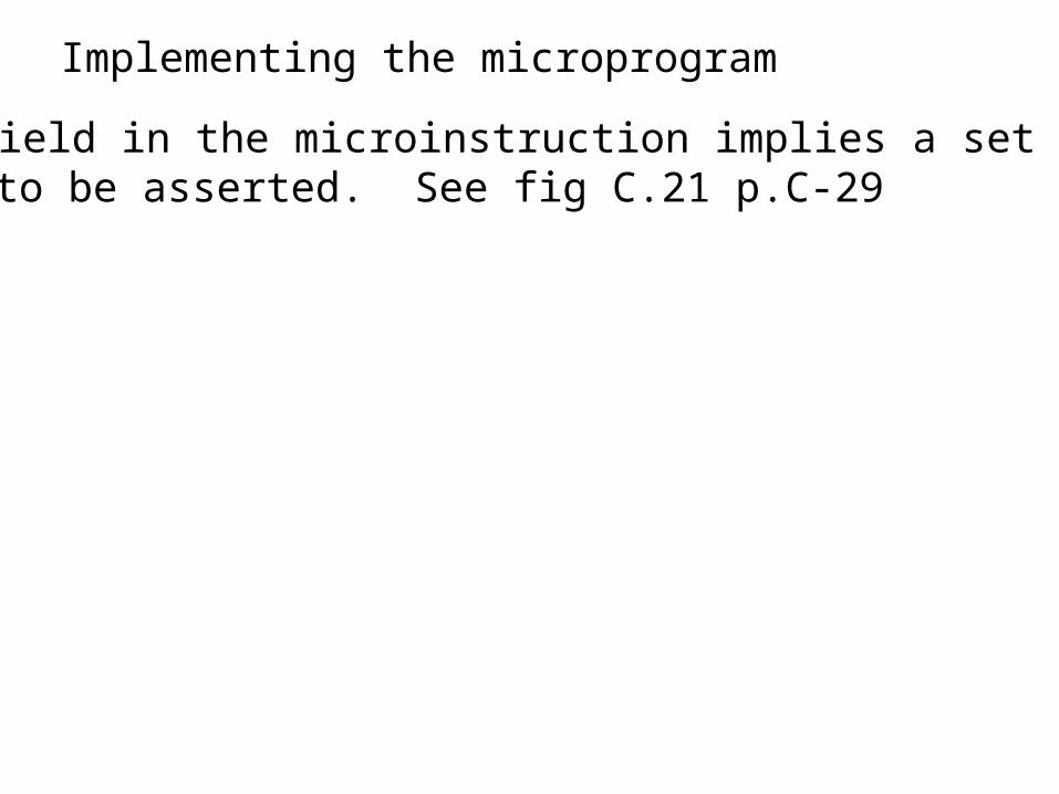
• Each field in the microinstruction implies a set of controlsignals to be asserted. See fig C.21 p.C-29
Implementing the microprogram
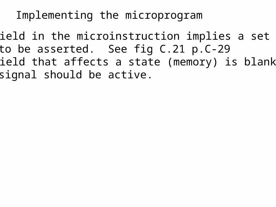
• Each field in the microinstruction implies a set of controlsignals to be asserted. See fig C.21 p.C-29• If a field that affects a state (memory) is blank, then nocontrol signal should be active.
Implementing the microprogram
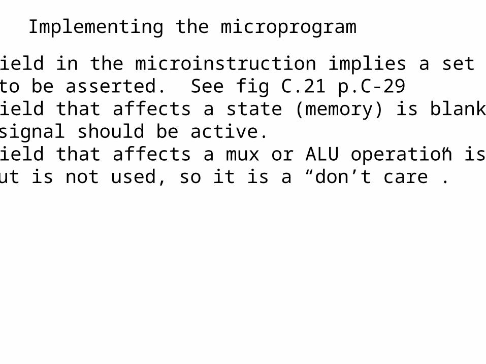
• Each field in the microinstruction implies a set of controlsignals to be asserted. See fig C.21 p.C-29• If a field that affects a state (memory) is blank, then nocontrol signal should be active.• If a field that affects a mux or ALU operation is blank,the output is not used, so it is a “don’t care”.
Implementing the microprogram
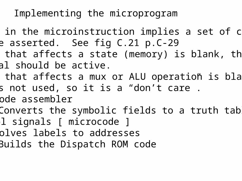
• Each field in the microinstruction implies a set of controlsignals to be asserted. See fig C.21 p.C-29• If a field that affects a state (memory) is blank, then nocontrol signal should be active.• If a field that affects a mux or ALU operation is blank,the output is not used, so it is a “don’t care”.• The microcode assembler 1. Converts the symbolic fields to a truth table for the
control signals [ microcode ] 2. Resolves labels to addresses
3. Builds the Dispatch ROM code
Implementing the microprogram
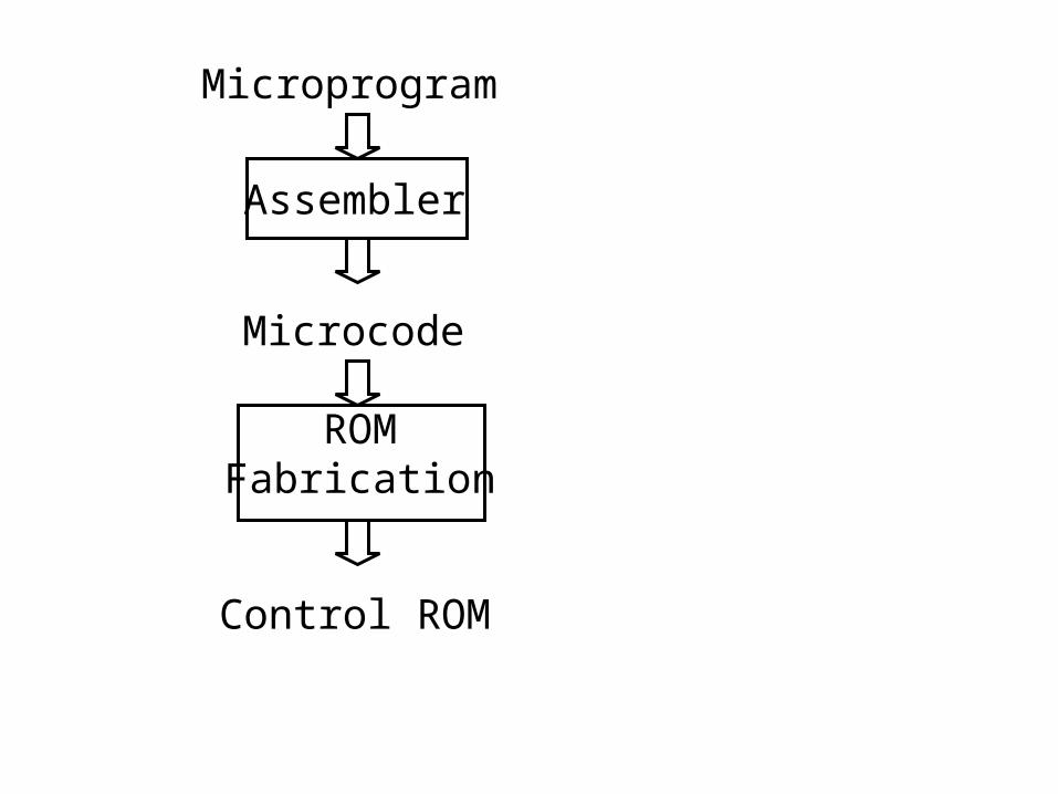
Microprogram
Assembler
Microcode
ROMFabrication
Control ROM
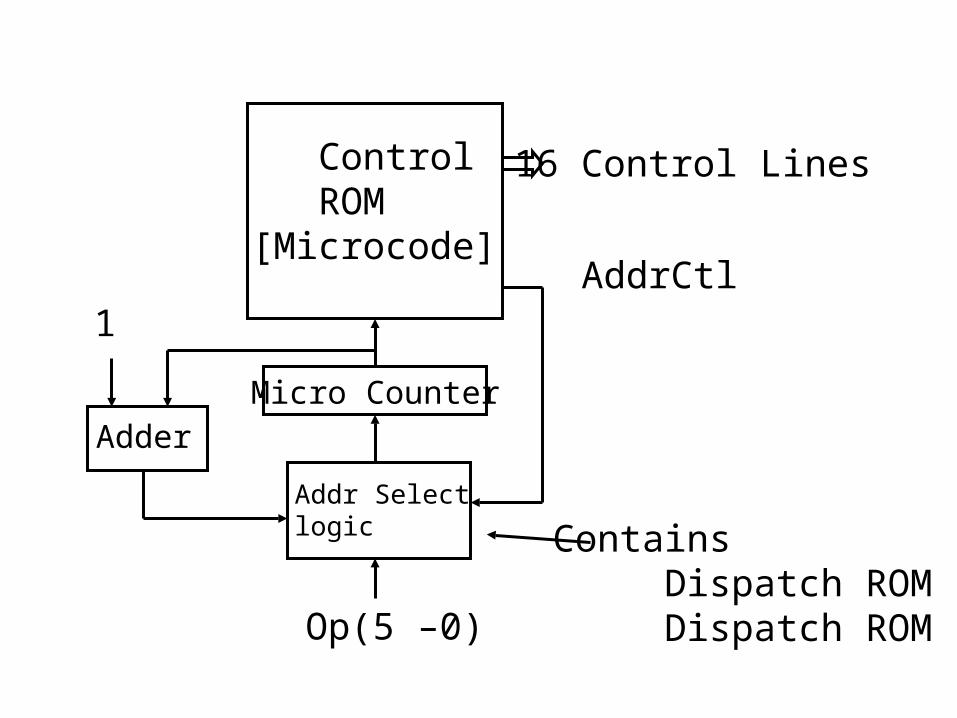
16 Control Lines Control ROM[Microcode]
Micro Counter
Adder
1
Addr Selectlogic
Op(5 –0)
AddrCtl
Contains Dispatch ROM 1 Dispatch ROM 2
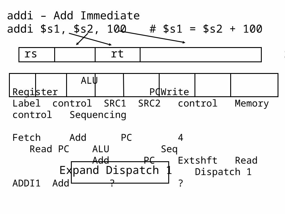
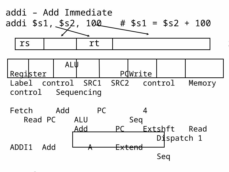
addi – Add Immediate addi $s1, $s2, 100 # $s1 = $s2 + 100
8 rs rt imm ALU Register PCWriteLabel control SRC1 SRC2 control Memory control Sequencing
Fetch Add PC 4 Read PC ALU Seq Add PC Extshft Read Dispatch 1ADDI1 Add ? ?
Expand Dispatch 1
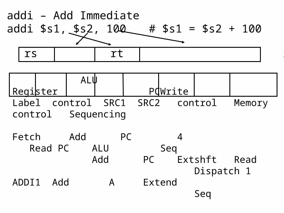
addi – Add Immediate addi $s1, $s2, 100 # $s1 = $s2 + 100
8 rs rt imm ALU Register PCWriteLabel control SRC1 SRC2 control Memory control Sequencing
Fetch Add PC 4 Read PC ALU Seq Add PC Extshft Read Dispatch 1ADDI1 Add A Extend Seq
addi – Add Immediate addi $s1, $s2, 100 # $s1 = $s2 + 100
8 rs rt imm ALU Register PCWriteLabel control SRC1 SRC2 control Memory control Sequencing
Fetch Add PC 4 Read PC ALU Seq Add PC Extshft Read Dispatch 1ADDI1 Add A Extend Seq ?
Write ALU uses rd field !
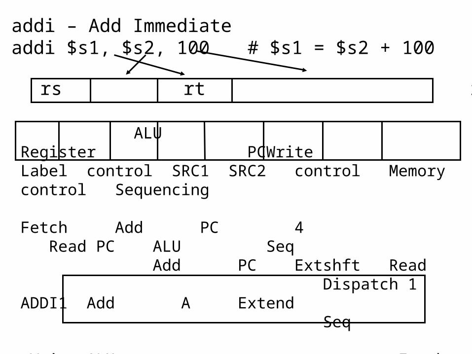
addi – Add Immediate addi $s1, $s2, 100 # $s1 = $s2 + 100
8 rs rt imm ALU Register PCWriteLabel control SRC1 SRC2 control Memory control Sequencing
Fetch Add PC 4 Read PC ALU Seq Add PC Extshft Read Dispatch 1ADDI1 Add A Extend Seq Write ALU rt Fetch
Write ALU uses rd field !Define: Write ALU rt = Write Reg[rt] with ALUOut
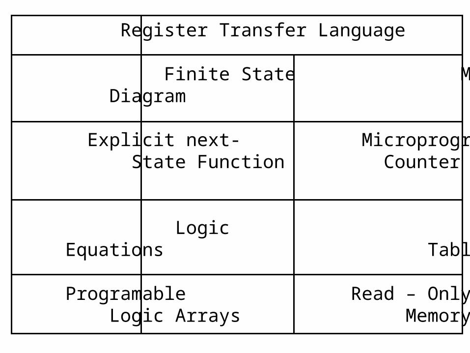
Design Tools Register Transfer Language
Initial Finite State MicroprogramRepresentation Diagram
Sequencing Explicit next- MicroprogramControl State Function Counter + Dispatch ROMs
Logic Logic TruthRepresentation Equations Tables
Implementation Programable Read – OnlyTechnique Logic Arrays Memory
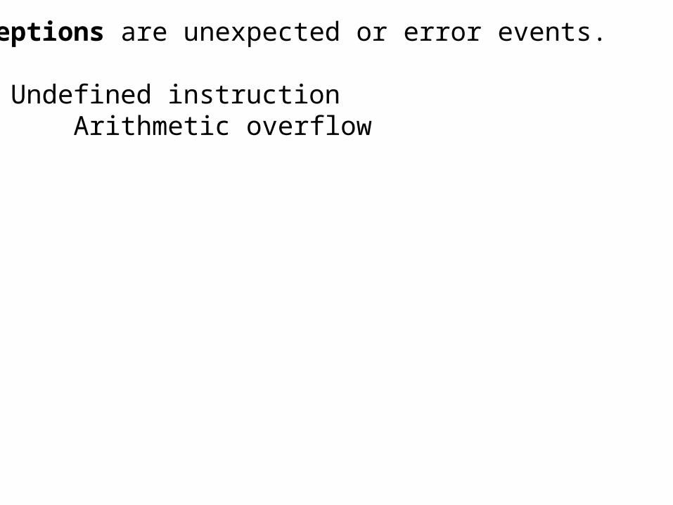
Exceptions are unexpected or error events.
Ex: Undefined instruction Arithmetic overflow
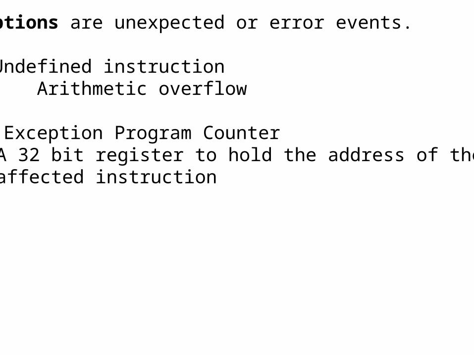
Exceptions are unexpected or error events.
Ex: Undefined instruction Arithmetic overflow
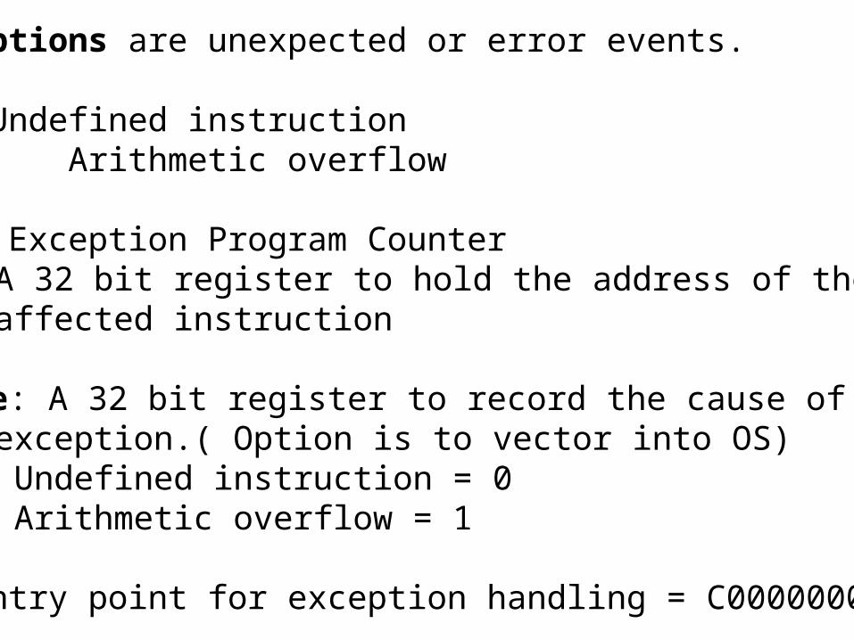
EPC: Exception Program CounterA 32 bit register to hold the address of theaffected instruction
Exceptions are unexpected or error events.
Ex: Undefined instruction Arithmetic overflow
EPC: Exception Program CounterA 32 bit register to hold the address of theaffected instruction
Cause: A 32 bit register to record the cause of theexception.( Option is to vector into OS) Undefined instruction = 0 Arithmetic overflow = 1
OS entry point for exception handling = C0000000 hex
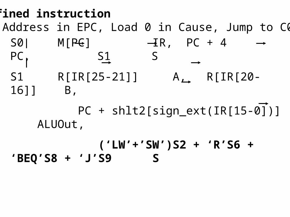
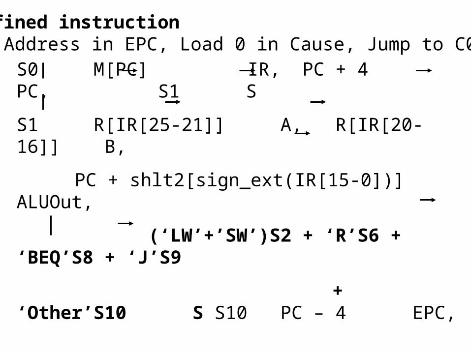
Undefined instructionSave Address in EPC, Load 0 in Cause, Jump to C0000000
S0 M[PC] IR, PC + 4 PC, S1 S
S1 R[IR[25-21]] A, R[IR[20-16]] B,
PC + shlt2[sign_ext(IR[15-0])] ALUOut,
(‘LW’+’SW’)S2 + ‘R’S6 + ‘BEQ’S8 + ‘J’S9 S
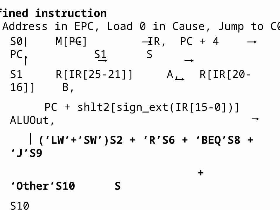
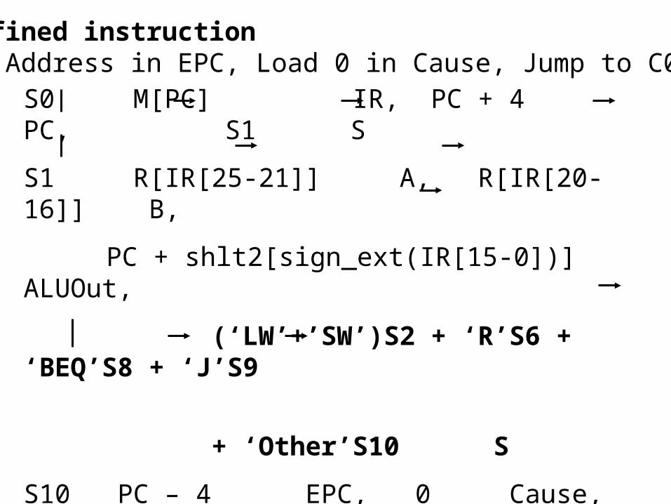
Undefined instructionSave Address in EPC, Load 0 in Cause, Jump to C0000000
S0 M[PC] IR, PC + 4 PC, S1 S
S1 R[IR[25-21]] A, R[IR[20-16]] B,
PC + shlt2[sign_ext(IR[15-0])] ALUOut,
(‘LW’+’SW’)S2 + ‘R’S6 + ‘BEQ’S8 + ‘J’S9
+ ‘Other’S10 S
S10
Undefined instructionSave Address in EPC, Load 0 in Cause, Jump to C0000000
S0 M[PC] IR, PC + 4 PC, S1 S
S1 R[IR[25-21]] A, R[IR[20-16]] B,
PC + shlt2[sign_ext(IR[15-0])] ALUOut,
(‘LW’+’SW’)S2 + ‘R’S6 + ‘BEQ’S8 + ‘J’S9
+ ‘Other’S10 S S10 PC – 4 EPC,
Undefined instructionSave Address in EPC, Load 0 in Cause, Jump to C0000000
S0 M[PC] IR, PC + 4 PC, S1 S
S1 R[IR[25-21]] A, R[IR[20-16]] B,
PC + shlt2[sign_ext(IR[15-0])] ALUOut,
(‘LW’+’SW’)S2 + ‘R’S6 + ‘BEQ’S8 + ‘J’S9
+ ‘Other’S10 S
S10 PC – 4 EPC, 0 Cause,
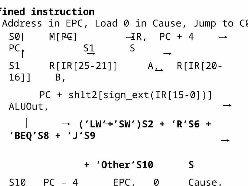
Undefined instructionSave Address in EPC, Load 0 in Cause, Jump to C0000000
S0 M[PC] IR, PC + 4 PC, S1 S
S1 R[IR[25-21]] A, R[IR[20-16]] B,
PC + shlt2[sign_ext(IR[15-0])] ALUOut,
(‘LW’+’SW’)S2 + ‘R’S6 + ‘BEQ’S8 + ‘J’S9
+ ‘Other’S10 S
S10 PC – 4 EPC, 0 Cause, C0000000 PC,
S0 S