Embed Size (px)
Citation preview

Examples

Copyright Notice Copyright 1994-2007 Agilent Technologies, Inc. All rights reserved.
Notice The information contained in this document is subject to change without notice.
Agilent Technologies makes no warranty of any kind with regard to this material, including, but not limited to, the implied warranties of merchantability and fitness for a particular purpose. Agilent Technologies shall not be liable for errors contained herein or for incidental or consequential damages in connection with the furnishing, performance, or use of this material.
Warranty A copy of the specific warranty terms that apply to this software product is available upon request from your Agilent Technologies representative.
U.S. Government Restricted Rights Software and technical data rights granted to the federal government include only those rights customarily provided to end user customers. Agilent provides this customary commercial license in Software and technical data pursuant to FAR 12.211 (Technical Data) and 12.212 (Computer Software) and, for the Department of Defense, DFARS 252.227-7015 (Technical Data - Commercial Items) and DFARS 227.7202-3 (Rights in Commercial Computer Software or Computer Software Documentation).
© Agilent Technologies, Inc. 1994-2007
395 Page Mill Road, Palo Alto, CA 94304 U.S.A.

Acknowledgments Mentor Graphics is a trademark of Mentor Graphics Corporation in the U.S. and other countries.
Microsoft®, Windows®, MS Windows®, Windows NT®, and MS-DOS® are U.S. registered trademarks of Microsoft Corporation.
Pentium® is a U.S. registered trademark of Intel Corporation.
PostScript® and Acrobat® are trademarks of Adobe Systems Incorporated.
UNIX® is a registered trademark of the Open Group.
Java(TM) is a U.S. trademark of Sun Microsystems, Inc.
SystemC® is a registered trademark of Open SystemC Initiative, Inc. in the United States and other countries and is used with permission.
Drawing Interchange file (DXF) is a trademark of Auto Desk, Inc.
EMPOWER/ML, GENESYS, SPECTRASYS, HARBEC, and TESTLINK are trademarks of Eagleware-Elanix Corporation.
GDSII is a trademark of Calma Company.
Sonnet is a registered trademark of Sonnet Software, Inc.
v
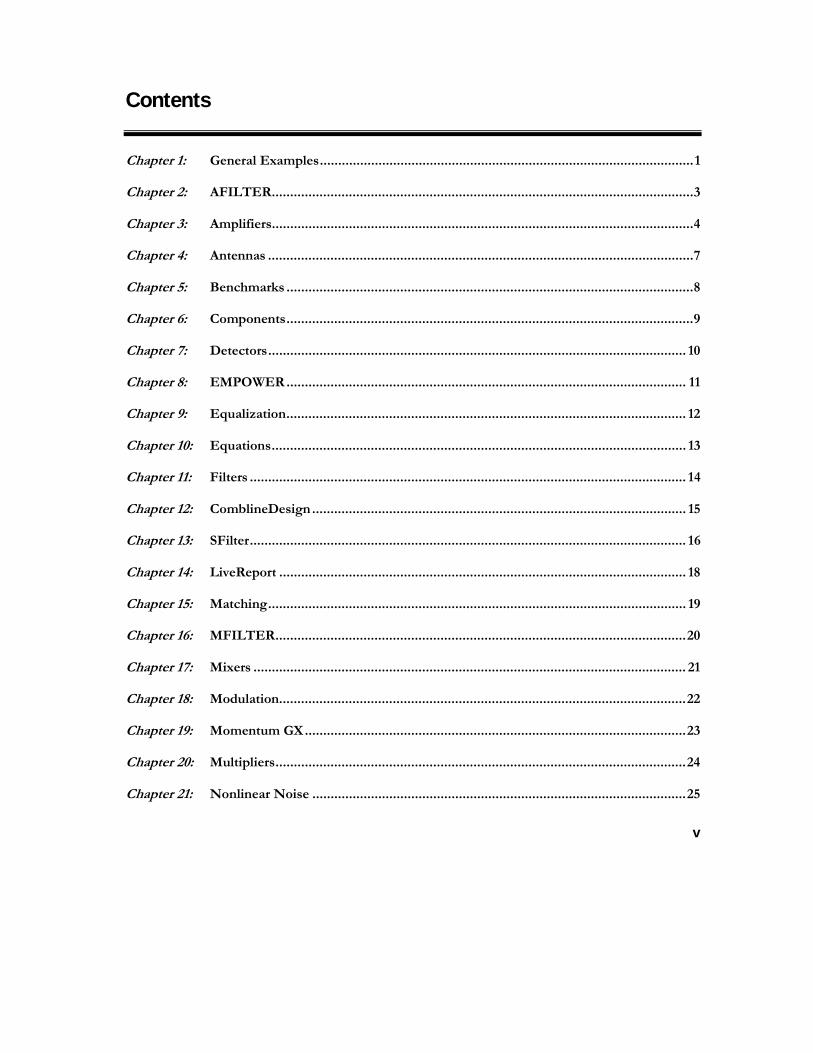
Contents
Chapter 1: General Examples......................................................................................................1
Chapter 2: AFILTER...................................................................................................................3
Chapter 3: Amplifiers...................................................................................................................4
Chapter 4: Antennas ....................................................................................................................7
Chapter 5: Benchmarks ...............................................................................................................8
Chapter 6: Components...............................................................................................................9
Chapter 7: Detectors.................................................................................................................. 10
Chapter 8: EMPOWER............................................................................................................. 11
Chapter 9: Equalization............................................................................................................. 12
Chapter 10: Equations................................................................................................................. 13
Chapter 11: Filters ....................................................................................................................... 14
Chapter 12: ComblineDesign...................................................................................................... 15
Chapter 13: SFilter....................................................................................................................... 16
Chapter 14: LiveReport ............................................................................................................... 18
Chapter 15: Matching.................................................................................................................. 19
Chapter 16: MFILTER................................................................................................................20
Chapter 17: Mixers ...................................................................................................................... 21
Chapter 18: Modulation...............................................................................................................22
Chapter 19: Momentum GX........................................................................................................23
Chapter 20: Multipliers................................................................................................................24
Chapter 21: Nonlinear Noise ......................................................................................................25

Examples
vi
Chapter 22: Oscillators ............................................................................................................... 26
Chapter 23: Scripting .................................................................................................................. 27
Chapter 24: Signal Control.......................................................................................................... 28
Chapter 25: SPECTRASYS ......................................................................................................... 29
Chapter 26: Spice ........................................................................................................................ 36
Chapter 27: Tutorial.................................................................................................................... 37
Chapter 28: VerilogA................................................................................................................... 39
Chapter 29: VIEWER ................................................................................................................. 40
Chapter 30: Examples With Additional Documentation.............................................................41
AFILTER.......................................................................................................................................... 41 Lowpass Minimum Inductor ..................................................................................................... 41 Lowpass Minimum Capacitor ................................................................................................... 44 Lowpass Single Feedback Tuning............................................................................................. 45 Lowpass Multiple Feedback ...................................................................................................... 47
Amplifiers.......................................................................................................................................... 48 Amplifier Feedback..................................................................................................................... 48 Amplifier Noise ........................................................................................................................... 50 Balanced Amplifier...................................................................................................................... 54 Bipolar Amplifier Optimized..................................................................................................... 59 Bipolar Common Emitter Amplifier........................................................................................ 61 Stability Circles............................................................................................................................. 63 Large Signal S Parameter Linear Test ...................................................................................... 68
Antennas ........................................................................................................................................... 71 Agile Antenna............................................................................................................................... 71 Array Driver ................................................................................................................................. 75 Patch Antenna.............................................................................................................................. 78 Simple Dipole Antenna .............................................................................................................. 80 Thin Loop Antenna .................................................................................................................... 84
Components ..................................................................................................................................... 87 BJT NL Model Fit ....................................................................................................................... 87 Box Models................................................................................................................................... 90 Coaxial Cable................................................................................................................................ 93 Negation Element........................................................................................................................ 96
Detectors........................................................................................................................................... 98 Simple Detector ........................................................................................................................... 98

Table Of Contents
vii
Equations ........................................................................................................................................ 102 S Parameters vs Swept Component ....................................................................................... 102 Spectral Analysis of Time domain data (wave2spec)........................................................... 104
Filters ............................................................................................................................................... 106 Contiguous Diplexer................................................................................................................. 106 Edge Coupled............................................................................................................................. 108 Gaussian Lowpass ..................................................................................................................... 111 Interdigital................................................................................................................................... 113 Tuned Bandpass ........................................................................................................................ 117 Xtal Filter .................................................................................................................................... 121 SFILTER .................................................................................................................................... 123
Matching.......................................................................................................................................... 158 Power Amp................................................................................................................................. 158 Simple Match.............................................................................................................................. 160
Mixer................................................................................................................................................ 161 Low Power Mixer...................................................................................................................... 161
Oscillators ....................................................................................................................................... 163 Cayenne: Oscillator Spurious Modes ..................................................................................... 163 Oscillator Node Voltages......................................................................................................... 167
Signal Control................................................................................................................................. 169 8 Way Splitter ............................................................................................................................. 169 Coupler with Asymmetrical Lines .......................................................................................... 172 Dual Mode Coupler .................................................................................................................. 175 Edge Coupler ............................................................................................................................. 178 Resistive Broadband 10dB Attenuator .................................................................................. 180 Resistive Broadband 20dB Attenuator .................................................................................. 182 Transformer Coupler ................................................................................................................ 184
SPECTRASYS ............................................................................................................................... 186 Feed Forward Amplifier........................................................................................................... 186 Quad Hybrid Matrix Amp ....................................................................................................... 190 TX and RX Chain...................................................................................................................... 194 TX Noise in RX Band .............................................................................................................. 197 Diversity TX and Hybrid Amp ............................................................................................... 201
Tutorials .......................................................................................................................................... 203 Tiny Amp Tutorial .................................................................................................................... 203 Comparison: Harbec vs. Cayenne........................................................................................... 204 Harbec Frequency Resolution................................................................................................. 207 Optimization to Minimize Harmonic Distortion ................................................................ 210 Optimization in Time-Domain ............................................................................................... 219 Monte Carlo with Equations Tutorial.................................................................................... 222
Index ............................................................................................................................... 227

1
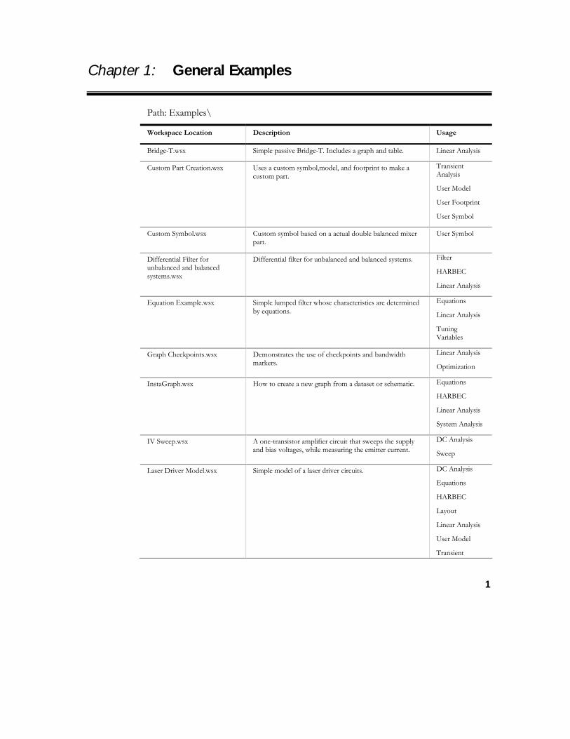
Chapter 1: General Examples
Path: Examples\
Workspace Location Description Usage
Bridge-T.wsx Simple passive Bridge-T. Includes a graph and table. Linear Analysis
Custom Part Creation.wsx Uses a custom symbol,model, and footprint to make a custom part.
Transient Analysis
User Model
User Footprint
User Symbol
Custom Symbol.wsx Custom symbol based on a actual double balanced mixer part.
User Symbol
Differential Filter for unbalanced and balanced systems.wsx
Differential filter for unbalanced and balanced systems. Filter
HARBEC
Linear Analysis
Equation Example.wsx Simple lumped filter whose characteristics are determined by equations.
Equations
Linear Analysis
Tuning Variables
Graph Checkpoints.wsx Demonstrates the use of checkpoints and bandwidth markers.
Linear Analysis
Optimization
InstaGraph.wsx How to create a new graph from a dataset or schematic. Equations
HARBEC
Linear Analysis
System Analysis
IV Sweep.wsx A one-transistor amplifier circuit that sweeps the supply and bias voltages, while measuring the emitter current.
DC Analysis
Sweep
Laser Driver Model.wsx Simple model of a laser driver circuits. DC Analysis
Equations
HARBEC
Layout
Linear Analysis
User Model
Transient

Examples
2
Analysis
Tuning Variables
Optimization Targets.wsx Demonstrates optimization targets on graphs. Optimization
TDR.wsx Uses CAYENNE on a TDR circuit Equations
Transient Analysis
Whats new.wsx Latest release features. New Features

categories
3
Chapter 2: AFILTER
Path: Examples\AFILTER
Workspace Location Description Usage
Lowpass Min C.wsx A fifth order lowpass minimum capacitor Chebyshev filter. For additional documentation see Lowpass Minimum Capacitor.
Linear Analysis Optimization Tuning Variables
Lowpass Min L.wsx A third order lowpass minimum inductor Chebyshev filter. Designed using LC/GIC transforms. For additional documentation see Lowpass Minimum Inductor..
Linear Analysis Optimization Tuning Variables
Lowpass Multiple Feedback.wsx A fifth order lowpass multiple feedback Chebyshev filter. For additonal documentation see Lowpass Multiple Feedback.
Linear Analysis Optimization Tuning Variables
Lowpass Single Feedback Tuning.wsx Low pass frequency characteristics of the first stage amplifier in a 4 stage amplifier circuit. For additional documentation see Lowpass Single Feedback Tuning.
Linear Analysis Graph Checkpoints Optimization Tuning variables
Lowpass With Optimization.wsx Starts with an 8th order Lowpass filter produced by Active Filter.
Linear Analysis Optimization Tuning Variables
Examples
4
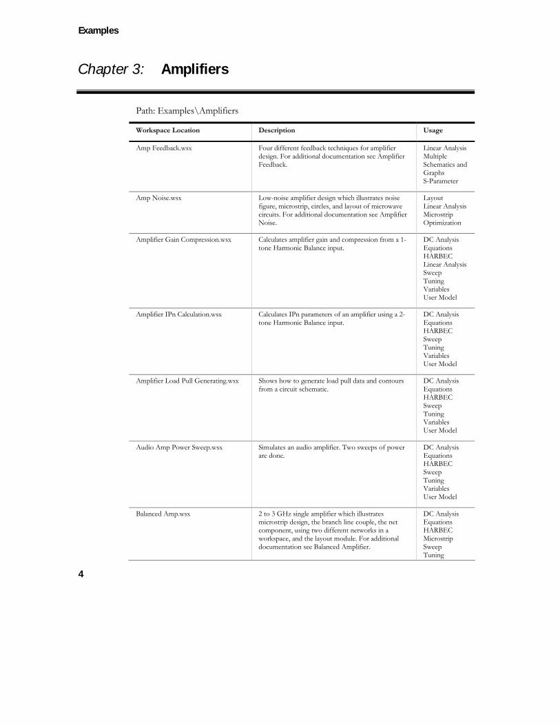
Chapter 3: Amplifiers
Path: Examples\Amplifiers
Workspace Location Description Usage
Amp Feedback.wsx Four different feedback techniques for amplifier design. For additional documentation see Amplifier Feedback.
Linear Analysis Multiple Schematics and Graphs S-Parameter
Amp Noise.wsx Low-noise amplifier design which illustrates noise figure, microstrip, circles, and layout of microwave circuits. For additional documentation see Amplifier Noise.
Layout Linear Analysis Microstrip Optimization
Amplifier Gain Compression.wsx Calculates amplifier gain and compression from a 1-tone Harmonic Balance input.
DC Analysis Equations HARBEC Linear Analysis Sweep Tuning Variables User Model
Amplifier IPn Calculation.wsx Calculates IPn parameters of an amplifier using a 2-tone Harmonic Balance input.
DC Analysis Equations HARBEC Sweep Tuning Variables User Model
Amplifier Load Pull Generating.wsx Shows how to generate load pull data and contours from a circuit schematic.
DC Analysis Equations HARBEC Sweep Tuning Variables User Model
Audio Amp Power Sweep.wsx Simulates an audio amplifier. Two sweeps of power are done.
DC Analysis Equations HARBEC Sweep Tuning Variables User Model
Balanced Amp.wsx 2 to 3 GHz single amplifier which illustrates microstrip design, the branch line couple, the net component, using two different networks in a workspace, and the layout module. For additional documentation see Balanced Amplifier.
DC Analysis Equations HARBEC Microstrip Sweep Tuning
categories
5
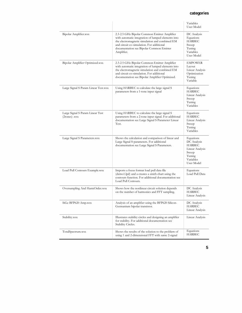
Variables User Model
Bipolar Amplifier.wsx 2.3-2.5 GHz Bipolar Common Emitter Amplifier with automatic integration of lumped elements into the electromagnetic simulation and combined EM and circuit co-simulation. For additional documentation see Bipolar Common Emitter Amplifier.
DC Analysis Equations HARBEC Sweep Tuning Variables User Model
Bipolar Amplifier Optimized.wsx 2.3-2.5 GHz Bipolar Common Emitter Amplifier with automatic integration of lumped elements into the electromagnetic simulation and combined EM and circuit co-simulation. For additional documentation see Bipolar Amplifier Optimized.
EMPOWER Layout Linear Analysis Optimization Tuning Variable
Large Signal S Param Linear Test.wsx Using HARBEC to calculate the large signal S parameters from a 1-tone input signal
Equations HARBEC Linear Analysis Sweep Tuning Variables
Large Signal S Param Linear Test (2tones) .wsx
Using HARBEC to calculate the large signal S parameters from a 2-tone input signal. For additional documentation see Large Signal S Parameter Linear Test.
Equations HARBEC Linear Analysis Sweep Tuning Variables
Large Signal S Parameters.wsx Shows the calculation and comparison of linear and Large Signal S-parameters. For additional documentation see Large Signal S Parameters.
Equations DC Analysis HARBEC Linear Analysis Sweep Tuning Variables User Model
Load Pull Contours Example.wsx Imports a focus format load pull data file (demo1.lpd) and a creates a smith chart using the contours function. For additional documentation see Load Pull Contours.
Equations Load Pull Data
Oversampling And HarmOrder.wsx Shows how the nonlinear circuit solution depends on the number of harmonics and FFT sampling.
DC Analysis HARBEC Linear Analysis
SiGe BFP620 Amp.wsx Analysis of an amplifier using the BFP620 Silicon-Germanium bipolar transistor.
DC Analysis HARBEC Linear Analysis
Stability.wsx Illustrates stability circles and designing an amplifier for stability. For additional documentation see Stability Circles.
Linear Analysis
TotalSpectrum.wsx Shows the results of the solution to the problem of using 1 and 2-dimensional FFT with same 2-signal
Equations HARBEC

Examples
6
frequencies.
categories
7
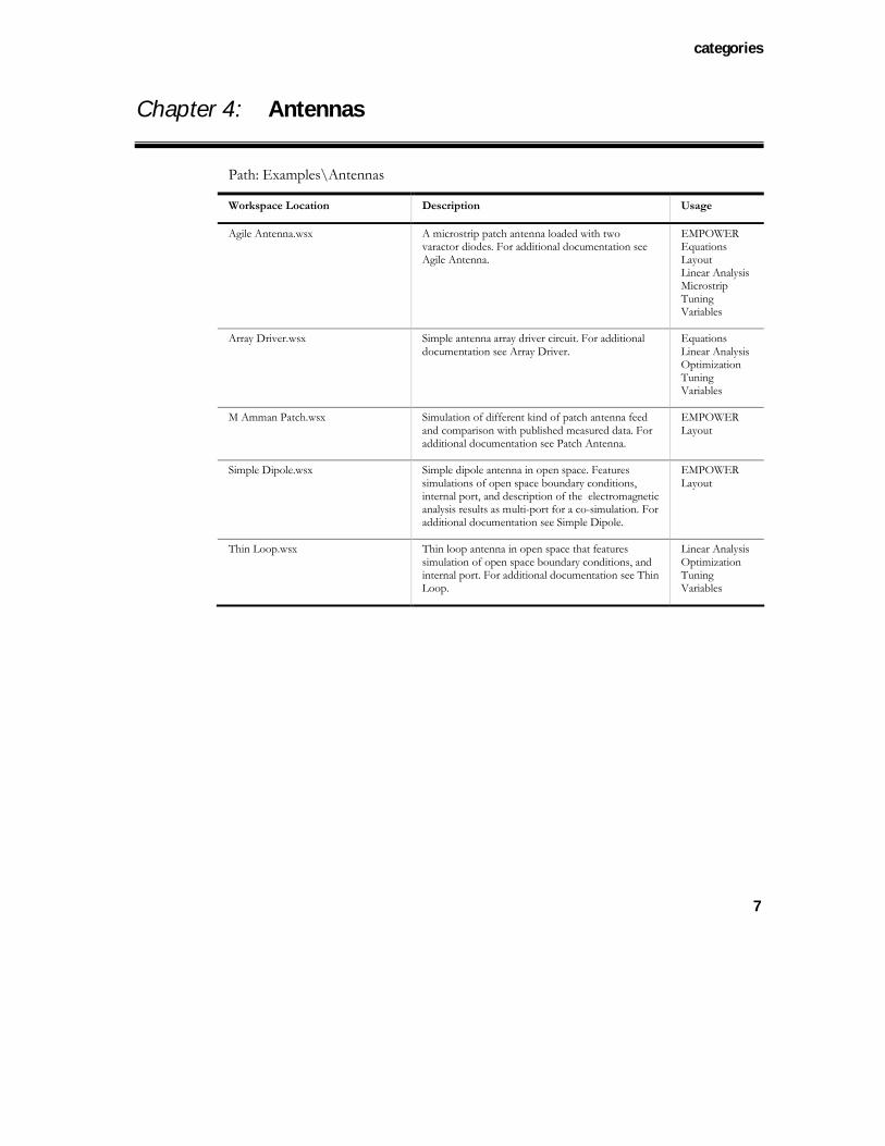
Chapter 4: Antennas
Path: Examples\Antennas
Workspace Location Description Usage
Agile Antenna.wsx A microstrip patch antenna loaded with two varactor diodes. For additional documentation see Agile Antenna.
EMPOWER Equations Layout Linear Analysis Microstrip Tuning Variables
Array Driver.wsx Simple antenna array driver circuit. For additional documentation see Array Driver.
Equations Linear Analysis Optimization Tuning Variables
M Amman Patch.wsx Simulation of different kind of patch antenna feed and comparison with published measured data. For additional documentation see Patch Antenna.
EMPOWER Layout
Simple Dipole.wsx Simple dipole antenna in open space. Features simulations of open space boundary conditions, internal port, and description of the electromagnetic analysis results as multi-port for a co-simulation. For additional documentation see Simple Dipole.
EMPOWER Layout
Thin Loop.wsx Thin loop antenna in open space that features simulation of open space boundary conditions, and internal port. For additional documentation see Thin Loop.
Linear Analysis Optimization Tuning Variables
Examples
8
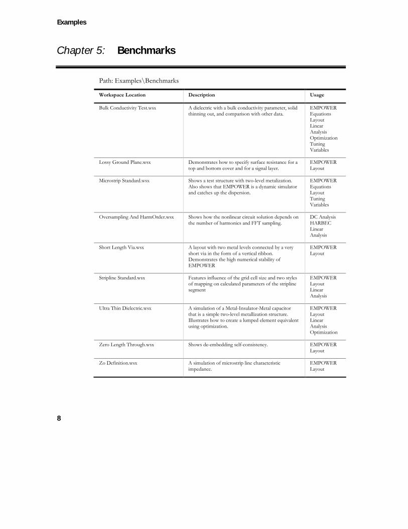
Chapter 5: Benchmarks
Path: Examples\Benchmarks
Workspace Location Description Usage
Bulk Conductivity Test.wsx A dielectric with a bulk conductivity parameter, solid thinning out, and comparison with other data.
EMPOWER Equations Layout Linear Analysis Optimization Tuning Variables
Lossy Ground Plane.wsx Demonstrates how to specify surface resistance for a top and bottom cover and for a signal layer.
EMPOWER Layout
Microstrip Standard.wsx Shows a test structure with two-level metalization. Also shows that EMPOWER is a dynamic simulator and catches up the dispersion.
EMPOWER Equations Layout Tuning Variables
Oversampling And HarmOrder.wsx Shows how the nonlinear circuit solution depends on the number of harmonics and FFT sampling.
DC Analysis HARBEC Linear Analysis
Short Length Via.wsx A layout with two metal levels connected by a very short via in the form of a vertical ribbon. Demonstrates the high numerical stability of EMPOWER
EMPOWER Layout
Stripline Standard.wsx Features influence of the grid cell size and two styles of mapping on calculated parameters of the stripline segment
EMPOWER Layout Linear Analysis
Ultra Thin Dielectric.wsx A simulation of a Metal-Insulator-Metal capacitor that is a simple two-level metallization structure. Illustrates how to create a lumped element equivalent using optimization.
EMPOWER Layout Linear Analysis Optimization
Zero Length Through.wsx Shows de-embedding self-consistency. EMPOWER Layout
Zo Definition.wsx A simulation of microstrip line characteristic impedance.
EMPOWER Layout

categories
9
Chapter 6: Components
Path: Examples\Components
Workspace Location Description Usage
Aperture Coupled Microstrip.wsx Features simulation of a structure with three metallization levels of different type and a comparison with measured and MoM data.
EMPOWER Layout
Big Planar Inductor.wsx An EM simulation of a spiral inductor with two internal z-directed ports to connect a circuit theory model of a bondwire in the co-simulation.
EMPOWER Equations Layout Linear Analysis
BJT NL Model Fit.wsx Shows how to compare and optimize a nonlinear SPICE model to measured S-parameters. For additional documentation see BJT NL Model Fit.
DC Analysis Equations Linear Analysis Optimization
Box Modes.wsx Explanation of the problems of box modes using EMPOWER. For additional documentation see Box Modes.
EMPOWER Layout
Coaxial Cable.wsx Uses manufacturer's data ( RG58.S2P ) to compute parameters for model. For additional documentation see Coaxial Cable.
Equations Import S-Data File Linear Analysis Optimization
Negation.wsx Demonstrates the use of the Negation element in removing ( or de-embedding) the effect of part of a measured network. For additional documentation see Negation Element.
Linear Analysis

Examples
10
Chapter 7: Detectors
Path: Examples\Detectors
Workspace Location Description Usage
Phase Detector.wsx Uses HARBEC on a Gilbert cell phase detector. HARBEC Sweep
Simple Detector.wsx A simple diode detector circuit. For additional documentation see Simple Detector.
DC Analysis HARBEC Sweep

categories
11
Chapter 8: EMPOWER
Path: Examples\EMPOWER
Workspace Location Description Usage
Layout Only.wsx Demonstrates EMPOWER electromagnetic simulation of a layout.
EMPOWER Layout
ViaThroughGround.wsx Two microstrip lines connected by a cylindrical via through the common ground.
EMPOWER
Layout

Examples
12
Chapter 9: Equalization
Path: Examples\Equalization
Workspace Location Description Usage
ShuntC.wsx Schematic was created by using FILTER Linear Analysis
ShuntC Complete.wsx Uses Equalize on a generated ShuntC filter. Equalize Linear Analysis
categories
13
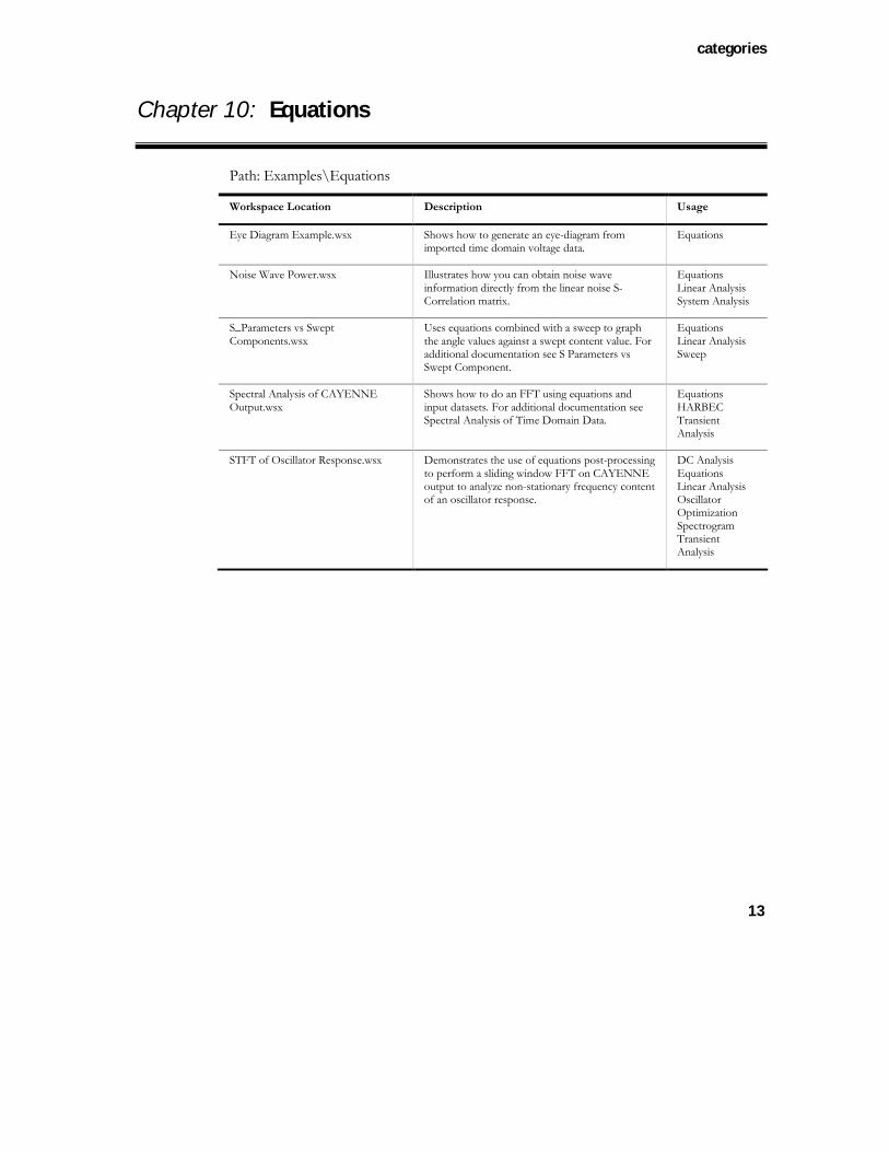
Chapter 10: Equations
Path: Examples\Equations
Workspace Location Description Usage
Eye Diagram Example.wsx Shows how to generate an eye-diagram from imported time domain voltage data.
Equations
Noise Wave Power.wsx Illustrates how you can obtain noise wave information directly from the linear noise S-Correlation matrix.
Equations Linear Analysis System Analysis
S_Parameters vs Swept Components.wsx
Uses equations combined with a sweep to graph the angle values against a swept content value. For additional documentation see S Parameters vs Swept Component.
Equations Linear Analysis Sweep
Spectral Analysis of CAYENNE Output.wsx
Shows how to do an FFT using equations and input datasets. For additional documentation see Spectral Analysis of Time Domain Data.
Equations HARBEC Transient Analysis
STFT of Oscillator Response.wsx Demonstrates the use of equations post-processing to perform a sliding window FFT on CAYENNE output to analyze non-stationary frequency content of an oscillator response.
DC Analysis Equations Linear Analysis Oscillator Optimization Spectrogram Transient Analysis
Examples
14
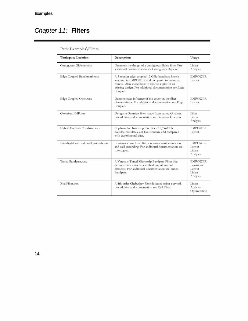
Chapter 11: Filters
Path: Examples\Filters
Workspace Location Description Usage
Contiguous Diplexer.wsx Illustrates the design of a contiguous diplex filter. For additional documentation see Contiguous Diplexer.
Linear Analysis
Edge Coupled Benchmark.wsx A 3-section edge-coupled 12 GHz bandpass filter is analyzed in EMPOWER and compared to measured results . Also shows how to choose a grid for an existing design. For additional documentation see Edge Coupled.
EMPOWER Layout
Edge Coupled Open.wsx Demonstrates influence of the cover on the filter characteristics. For additional documentation see Edge Coupled.
EMPOWER Layout
Gaussian_12dB.wsx Designs a Gaussian filter shape from stored G values. For additional documentation see Gaussian Lowpass.
Filter Linear Analysis
Hybrid Coplanar Bandstop.wsx Coplanar line bandstop filter for a 18/36-GHz doubler. Simulates slot-like structure and compares with experimental data.
EMPOWER Layout
Interdigital with side wall grounds.wsx Contains a low loss filter, a non-resonant simulation, and wall grounding. For additional documentation see Interdigital.
EMPOWER Layout Linear Analysis
Tuned Bandpass.wsx A Varactor-Tuned Microstrip Bandpass Filter that demonstrates automatic embedding of lumped elements. For additional documentation see Tuned Bandpass.
EMPOWER Equations Layout Linear Analysis
Xtal Filter.wsx A 4th order Chebyshev filter designed using a crystal. For additional documentation see Xtal Filter.
Linear Analysis Optimization
categories
15
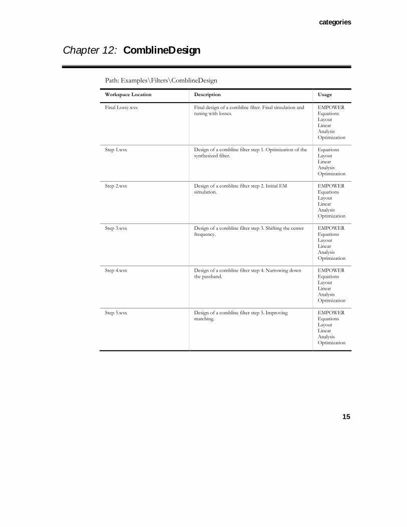
Chapter 12: ComblineDesign
Path: Examples\Filters\ComblineDesign
Workspace Location Description Usage
Final Lossy.wsx Final design of a combline filter. Final simulation and tuning with losses.
EMPOWER Equations Layout Linear Analysis Optimization
Step 1.wsx Design of a combline filter step 1. Optimization of the synthesized filter.
Equations Layout Linear Analysis Optimization
Step 2.wsx Design of a combline filter step 2. Initial EM simulation.
EMPOWER Equations Layout Linear Analysis Optimization
Step 3.wsx Design of a combline filter step 3. Shifting the center frequency.
EMPOWER Equations Layout Linear Analysis Optimization
Step 4.wsx Design of a combline filter step 4. Narrowing down the passband.
EMPOWER Equations Layout Linear Analysis Optimization
Step 5.wsx Design of a combline filter step 5. Improving matching.
EMPOWER Equations Layout Linear Analysis Optimization
Examples
16
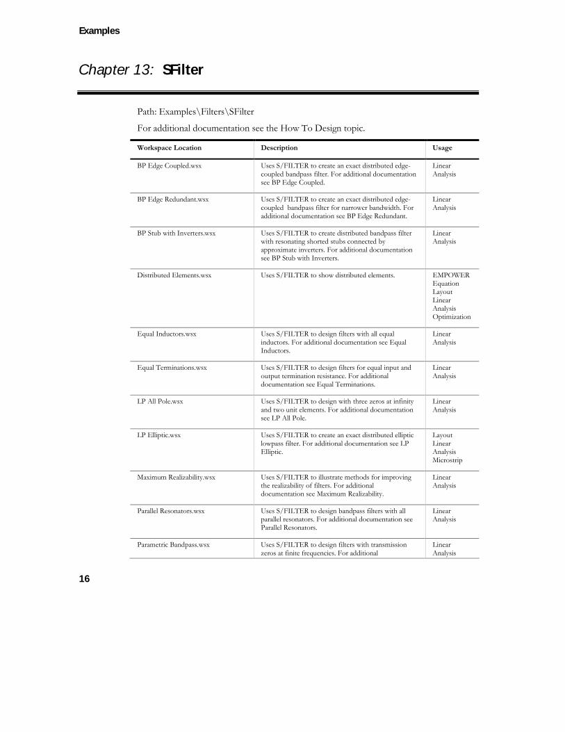
Chapter 13: SFilter
Path: Examples\Filters\SFilter
For additional documentation see the How To Design topic.
Workspace Location Description Usage
BP Edge Coupled.wsx Uses S/FILTER to create an exact distributed edge-coupled bandpass filter. For additional documentation see BP Edge Coupled.
Linear Analysis
BP Edge Redundant.wsx Uses S/FILTER to create an exact distributed edge-coupled bandpass filter for narrower bandwidth. For additional documentation see BP Edge Redundant.
Linear Analysis
BP Stub with Inverters.wsx Uses S/FILTER to create distributed bandpass filter with resonating shorted stubs connected by approximate inverters. For additional documentation see BP Stub with Inverters.
Linear Analysis
Distributed Elements.wsx Uses S/FILTER to show distributed elements. EMPOWER Equation Layout Linear Analysis Optimization
Equal Inductors.wsx Uses S/FILTER to design filters with all equal inductors. For additional documentation see Equal Inductors.
Linear Analysis
Equal Terminations.wsx Uses S/FILTER to design filters for equal input and output termination resistance. For additional documentation see Equal Terminations.
Linear Analysis
LP All Pole.wsx Uses S/FILTER to design with three zeros at infinity and two unit elements. For additional documentation see LP All Pole.
Linear Analysis
LP Elliptic.wsx Uses S/FILTER to create an exact distributed elliptic lowpass filter. For additional documentation see LP Elliptic.
Layout Linear Analysis Microstrip
Maximum Realizability.wsx Uses S/FILTER to illustrate methods for improving the realizability of filters. For additional documentation see Maximum Realizability.
Linear Analysis
Parallel Resonators.wsx Uses S/FILTER to design bandpass filters with all parallel resonators. For additional documentation see Parallel Resonators.
Linear Analysis
Parametric Bandpass.wsx Uses S/FILTER to design filters with transmission zeros at finite frequencies. For additional
Linear Analysis
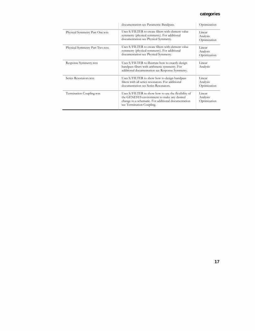
categories
17
documentation see Parametric Bandpass. Optimization
Physical Symmetry Part One.wsx Uses S/FILTER to create filters with element value symmetry (physical symmetry). For additional documentation see Physical Symmetry.
Linear Analysis Optimization
Physical Symmetry Part Two.wsx Uses S/FILTER to create filters with element value symmetry (physical symmetry). For additional documentation see Physical Symmetry.
Linear Analysis Optimization
Response Symmetry.wsx Uses S/FILTER to illustrate how to exactly design bandpass filters with arithmetic symmetry. For additional documentation see Response Symmetry.
Linear Analysis
Series Resonators.wsx Uses S/FILTER to show how to design bandpass filters with all series resonators. For additional documentation see Series Resonators.
Linear Analysis Optimization
Termination Coupling.wsx Uses S/FILTER to show how to use the flexibility of the GENESYS environment to make any desired change to a schematic. For additional documentation see Termination Coupling.
Linear Analysis Optimization
Examples
18
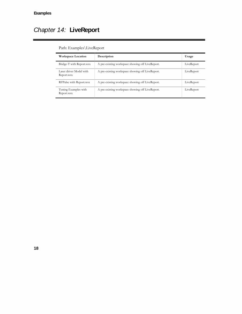
Chapter 14: LiveReport
Path: Examples\LiveReport
Workspace Location Description Usage
Bridge-T with Report.wsx A pre-existing workspace showing off LiveReport. LiveReport
Laser driver Model with Report.wsx
A pre-existing workspace showing off LiveReport. LiveReport
RFPulse with Report.wsx A pre-existing workspace showing off LiveReport. LiveReport
Tuning Examples with Report.wsx
A pre-existing workspace showing off LiveReport. LiveReport

categories
19
Chapter 15: Matching
Path: Examples\Matching
Workspace Location Description Usage
Optimal Matching.wsx Shows off the port power measurement. Equations HARBEC Sweep Tuning Variable
PowerAmp.wsx Illustrates power amplifier design of a Motorola MRF559 amplifier. For additional documentation see Power Amp.
Impedance Match Linear Analysis Optimization User Models
Simple Match.wsx Demonstrates a simple impedance match. For additional documentation see Simple Match.
Impedance Match Linear Analysis Optimization

Examples
20
Chapter 16: MFILTER
Path: Examples\MFILTER
Workspace Location Description Usage
BPF Chebyshev 1625 2875 MHz Contains an Chebyshev interdigital bandpass created by using MFilter.
EMPOWER Equations Layout Linear Analysis MFilter Optimization Tuning Variables

categories
21
Chapter 17: Mixers
Path: Examples\Mixers
Workspace Location Description Usage
Diode Ring Mixer.wsx Example of using HARBEC on a simple double-balanced diode ring mixer.
Equations HARBEC Filter Linear Analysis Sweep Tuning Variables
Double Balance Gilbert cell mixer.wsx
HARBEC example of a Gilbert Cell mixer. Demonstrates the hb_spurious function.
DC Analysis Equations HARBEC Sweep Tuning Variable
Gilbert cell BJT mixer.wsx HARBEC example of a Gilbert cell BJT mixer DC Analysis Equations HARBEC Sweep Tuning Variable
Mixer_Design_1.wsx Uses the Mixer Synthesis tool to develop and test a mixer design with a SPICE model for the active device in place of the default generic model.
HARBEC Mixer Sweep Tuning Variables
Mixer_Design_2.wsx Uses the Mixer and Oscillator Synthesis tools to develop and test a mixer design with an associated local oscillator. SPICE models were used for the nonlinear devices.
DC Analysis HARBEC Mixer Oscillator Optimization Sweep Transient Analysis Tuning Variables
Rat_race_1GHz_Mixer.wsx Demonstrate the ability to design RF mixers. HARBEC Sweep

Examples
22
Chapter 18: Modulation
Path: Examples\Modulation
Workspace Location Description Usage
Modulated Sources A simple diode-capacitor demodulator operates on an AM modulated signal to produce an output at the source frequency while removing the carrier.
Equations HARBEC Transient Analysis
categories
23
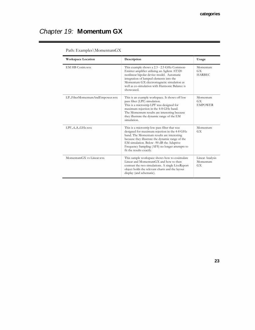
Chapter 19: Momentum GX
Path: Examples\MomentumGX
Workspace Location Description Usage
EM HB Cosim.wsx This example shows a 2.3 - 2.5 GHz Common-Emitter amplifier utilizing an Agilent AT320 nonlinear bipolar device model. Automatic integration of lumped elements into the Momentum GX electromagnetic simulation as well as co-simulation with Harmonic Balance is showcased.
Momentum GX HARBEC
LP_FilterMomentumAndEmpower.wsx This is an example workspace. It shows off low pass filter (LPF) simulation. This is a microstrip LPF was designed for maximum rejection in the 4-8 GHz band. The Momentum results are interesting because they illustrate the dynamic range of the EM simulation.
Momentum GX EMPOWER
LPF_4_8_GHz.wsx This is a microstrip low pass filter that was designed for maximum rejection in the 4-8 GHz band. The Momentum results are interesting because they illustrate the dynamic range of the EM simulation. Below -90 dB the Adaptive Frequency Sampling (AFS) no longer attempts to fit the results exactly.
Momentum GX
MomentumGX vs Linear.wsx This sample workspace shows how to cosimulate Linear and MomentumGX and how to then contrast the two simulations. A single LiveReport object holds the relevant charts and the layout display (and schematic).
Linear Analysis Momentum GX

Examples
24
Chapter 20: Multipliers
Path: Examples\Multipliers
Workspace Location Description Usage
BJT tripler.wsx HARBEC of a BJT frequency multiplier. DC Analysis Equations HARBEC Linear Analysis Tuning Variables User Models
BJT_ tripler Optimized.wsx HARBEC of a BJT frequency multiplier with optimization and output equizations to allow experimentation of different goals.
DC Analysis Equations HARBEC Optimization Linear Analysis Tuning Variables User Models
BJT_Doubler.wsx HARBEC of a BJT passive frequency doubler HARBEC

categories
25
Chapter 21: Nonlinear Noise
Path: Examples\Nonlinear Noise
Workspace Location Description Usage
BJT tripler Noise.wsx Nonlinear noise analysis of a BJT frequency multiplier.
DC Analysis Equations HARBEC Linear Analysis Sweep Tuning Variables User Models
Noise Diode Ring Mixer.wsx Nonlinear noise simulation of a diode mixer. Equations HARBEC Filter Linear Analysis Sweep Tuning Variables
NoiseClappJFETosc.wsx Demonstrates oscillator SSB noise simulation. DC Analysis HARBEC Oscillator Simulation Tuning Variables
Pierce Crystal Osc Noise.wsx Shows HARBEC Oscillator Analysis for a Crystal Oscillator Simulation, including nonlinear noise analysis.
HARBEC Oscillator Simulation
SiGe BFP620 Amp Noise.wsx Shows the nonlinear noise simulation of a BFP620 Silicon-Germanium bipolar transistor.
DC Analysis Equations HARBEC Linear Analysis Sweep Tuning Variable User Model
Simple Detector Noise.wsx Contains a nonlinear simulation of a simple diode detector circuit using HARBEC, and includes a nonlinear noise analysis.
DC Analysis Equations HARBEC Sweep Tuning Variables

Examples
26
Chapter 22: Oscillators
Path: Examples\Oscillators
Workspace Location Description Usage
Colpitts Oscillator.wsx HARBEC Oscillator Analysis for a Colpitts oscillator with and without an external signal.
DC Analysis Equations HARBEC Oscillator Analysis Transient Analysis User Model
Negative resistor oscillator.wsx Models a negative resistor oscillator with HARBEC Oscillator Analysis.
Equations HARBEC Oscillator Analysis
Osc wave2spec.wsx Demonstrates the use of the wave2spec function which calculates the spectrum of an oscillator output voltage wave from Transient analysis data
Equations HARBEC Oscillator Analysis Transient Analysis Tuning Variables
Oscillator Node Voltage.wsx Simulates voltages using HARBEC or CAYENNE. For additional documentation see Oscillator Node Voltages.
DC Analysis Linear Analysis Transient Analysis
Oscillator Spurious Models.wsx Illustrates using CAYENNE to simulate and manage oscillator spurious mode. For additional documentation see Cayenne: Oscillator Spurious Modes.
DC Analysis Linear Analysis Transient Analysis
Oscillator_Design_1.wsx Synthesizes and tests an oscillator, then designs a filter to remove unwanted harmonics from the oscillator output.
DC Analysis Equations Filter Linear Analysis Oscillator Optimization Transient Analysis Tuning Variables
Oscillator_Design_2.wsx Synthesizes and tests an oscillator design with a SPICE model for the active device in place of the default generic model.
DC Analysis Linear Analysis Oscillator Optimization Transient Analysis Tuning Variables
Pierce Crystal Osc Mixer.wsx HARBEC Oscillator Analysis for a Crystal Oscillator with external exitation ( self oscillating mixer ).
HARBEC Oscillator Analysis
categories
27
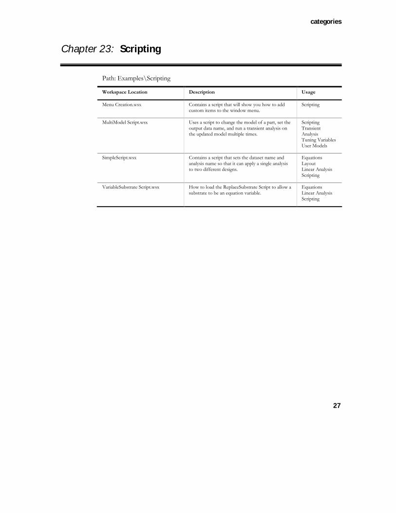
Chapter 23: Scripting
Path: Examples\Scripting
Workspace Location Description Usage
Menu Creation.wsx Contains a script that will show you how to add custom items to the window menu.
Scripting
MultiModel Script.wsx Uses a script to change the model of a part, set the output data name, and run a transient analysis on the updated model multiple times.
Scripting Transient Analysis Tuning Variables User Models
SimpleScript.wsx Contains a script that sets the dataset name and analysis name so that it can apply a single analysis to two different designs.
Equations Layout Linear Analysis Scripting
VariableSubstrate Script.wsx How to load the ReplaceSubstrate Script to allow a substrate to be an equation variable.
Equations Linear Analysis Scripting
Examples
28
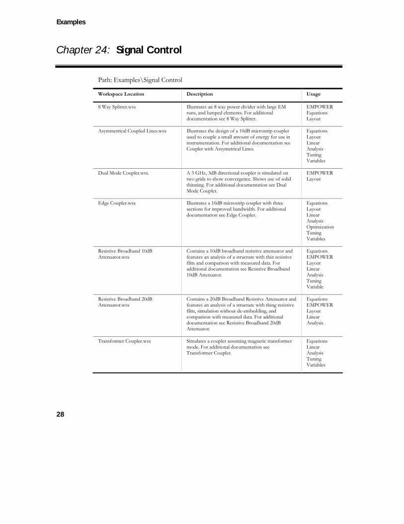
Chapter 24: Signal Control
Path: Examples\Signal Control
Workspace Location Description Usage
8 Way Splitter.wsx Illustrates an 8 way power divider with large EM runs, and lumped elements. For additional documentation see 8 Way Splitter.
EMPOWER Equations Layout
Asymmetrical Coupled Lines.wsx Illustrates the design of a 10dB microstrip coupler used to couple a small amount of energy for use in instrumentation. For additional documentation see Coupler with Assymetrical Lines.
Equations Layout Linear Analysis Tuning Variables
Dual Mode Coupler.wsx A 3 GHz, 3dB directional coupler is simulated on two grids to show convergence. Shows use of solid thinning. For additional documentation see Dual Mode Coupler.
EMPOWER Layout
Edge Coupler.wsx Illustrates a 10dB microstrip coupler with three sections for improved bandwidth. For additional documentation see Edge Coupler.
Equations Layout Linear Analysis Optimization Tuning Variables
Resistive Broadband 10dB Attenuator.wsx
Contains a 10dB broadband resistive attenuator and features an analysis of a structure with thin resistive film and comparison with measured data. For additional documentation see Resistive Broadband 10dB Attenuator.
Equations EMPOWER Layout Linear Analysis Tuning Variable
Resistive Broadband 20dB Attenuator.wsx
Contains a 20dB Broadband Resistive Attenuator and features an analysis of a structure with thing resistive film, simulation without de-embedding, and comparison with measured data. For additional documentation see Resistive Broadband 20dB Attenuator.
Equations EMPOWER Layout Linear Analysis
Transformer Coupler.wsx Simulates a coupler assuming magnetic transformer mode. For additional documentation see Transformer Coupler.
Equations Linear Analysis Tuning Variables
categories
29
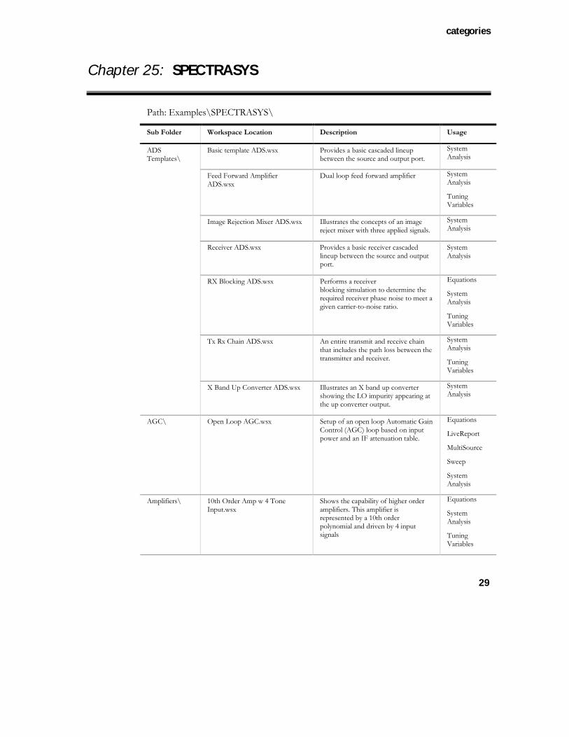
Chapter 25: SPECTRASYS
Path: Examples\SPECTRASYS\
Sub Folder Workspace Location Description Usage
Basic template ADS.wsx Provides a basic cascaded lineup between the source and output port.
System Analysis
Feed Forward Amplifier ADS.wsx
Dual loop feed forward amplifier System Analysis
Tuning Variables
Image Rejection Mixer ADS.wsx Illustrates the concepts of an image reject mixer with three applied signals.
System Analysis
Receiver ADS.wsx Provides a basic receiver cascaded lineup between the source and output port.
System Analysis
RX Blocking ADS.wsx Performs a receiver blocking simulation to determine the required receiver phase noise to meet a given carrier-to-noise ratio.
Equations
System Analysis
Tuning Variables
Tx Rx Chain ADS.wsx An entire transmit and receive chain that includes the path loss between the transmitter and receiver.
System Analysis
Tuning Variables
ADS Templates\
X Band Up Converter ADS.wsx Illustrates an X band up converter showing the LO impurity appearing at the up converter output.
System Analysis
AGC\ Open Loop AGC.wsx Setup of an open loop Automatic Gain Control (AGC) loop based on input power and an IF attenuation table.
Equations
LiveReport
MultiSource
Sweep
System Analysis
Amplifiers\ 10th Order Amp w 4 Tone Input.wsx
Shows the capability of higher order amplifiers. This amplifier is represented by a 10th order polynomial and driven by 4 input signals
Equations
System Analysis
Tuning Variables
Examples
30
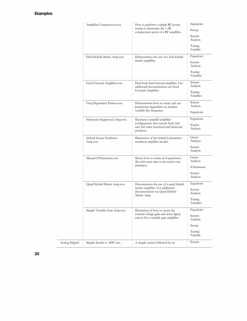
Amplifier Compression.wsx How to perform a simple RF power sweep to determine the 1 dB compression point of a RF amplifier.
Equations
Sweep
System Analysis
Tuning Variable
Dual Hybrid Matrix Amp.wsx Demonstrates the use of a dual hybrid matrix amplifier.
Equations
System Analysis
Tuning Variables
Feed Forward Amplifier.wsx Dual loop feed forward amplifier. For additional documentation see Feed Forward Amplifier.
System Analysis
Tuning Variables
Freq Dependent Params.wsx Demonstrates how to create and use parameters dependent on another variable like frequency.
System Analysis
Equations
Harmonic Suppressed Amp.wsx Illustrates a parallel amplifier configuration that cancels both 2nd and 3rd order intermod and harmonic products.
Equations
System Analysis
Hybrid Linear Nonlinear Amp.wsx
Illustration of the hybrid S parameter nonlinear amplifier model.
Linear Analysis
System Analysis
Manual S Parameters.wsx Shows how to create an S-parameter file with noise data to be used in the simulator.
Linear Analysis
S-Parameter
System Analysis
Quad Hybrid Matrix Amp.wsx Demonstrates the use of a quad hybrid matrix amplifier. For additional documentation see Quad Hybrid Matrix Amp.
Equations
System Analysis
Tuning Variables
Simple Variable Gain Amp.wsx Illustration of how to create the control voltage gain and noise figure curves for a variable gain amplifier.
Equations
System Analysis
Sweep
Tuning Variable
Analog Digital\ Simple System w ADC.wsx A simple system followed by an System
categories
31
impedance matched analog-to-digital converter.
Analysis
Tuning Variable
AppCAD\ AppCAD 1.9Ghz CDMA Handset Receiver.wsx
Illustration of how a dumbed down SPECTRASYS simulation will give the same answers as the AppCAD NoiseCalc example '1.9 GHz Handset Receiver'.
System Analysis
Coherency\ Reference Clock.wsx Shows how coherency and the source reference clock works in SPECTRASYS
Coherency
MultiSource
System Analysis
Spectrum Mask.wsx Creates limit lines from an array of numbers used for a spectrum mask.
Equations
System Analysis
Equations\
User Defined Warnings.wsx Uses equations to create a user defined warning and error messages.
Equations
System Analysis
Tuning Variable
Freq Mult Div\ Multiplier Divider SSB Decomposition.wsx
Shows how an unwanted single sideband signal at the input of a digital divider (or frequency multiplier or divider) is decomposed into its AM and PM components
MultiSource
System Analysis
Tuning Variables
Group Delay Verification.wsx Shows how group delay measurements in the linear analysis engine are the same as SPECTRASYS.
Equations
Linear Analysis
System Analysis
Group Delay\
RXSystem Group Delay.wsx Shows how to get SPECTRASYS group delay measurements.
Equations
Linear Analysis
System Analysis
IC Design\ Simple Receiver IC.wsx Shows voltage based measurements and models used in IC design.
System Analysis
Basic IP2 and IP3 Measurements.wsx
How to perform an IP2 and IP3 measurement on the same circuit at the same time.
System Analysis
Intermods\
Intermod Basics.wsx How to perform both in-band and out-of-band intermod analysis.
System Analysis
Examples
32
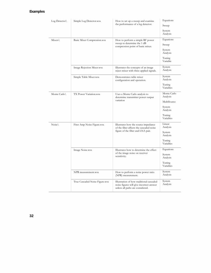
Log Detector\ Simple Log Detector.wsx How to set up a sweep and examine the performance of a log detector.
Equations
Sweep
System Analysis
Basic Mixer Compression.wsx How to perform a simple RF power sweep to determine the 1 dB compression point of basic mixer.
Equations
Sweep
System Analysis
Tuning Variable
Image Rejection Mixer.wsx Illustrates the concepts of an image reject mixer with three applied signals.
System Analysis
Mixers\
Simple Table Mixer.wsx Demonstrates table mixer configuration and operation.
System Analysis
Tuning Variables
Monte Carlo\ TX Power Variation.wsx Uses a Monte Carlo analysis to determine transmitter power output variation
Monte Carlo Analysis
MultiSource
System Analysis
Tuning Variables
Fiter Amp Noise Figure.wsx Illustrates how the source impedance of the filter affects the cascaded noise figure of the filter and LNA pair.
Linear Analysis
System Analysis
Tuning Variables
Image Noise.wsx Illustrates how to determine the effect of the image noise on receiver sensitivity.
Equations
System Analysis
Tuning Variables
NPR measurement.wsx How to perform a noise power ratio (NPR) measurement.
System Analysis
Noise\
True Cascaded Noise Figure.wsx Illustration of how traditional cascaded noise figures will give incorrect answer unless all paths are considered.
System Analysis
categories
33
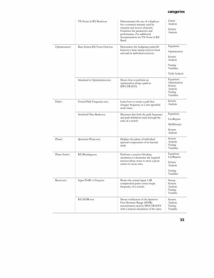
TX Noise in RX Band.wsx Demonstrates the use of a duplexer for a common antenna used by transmit and receive channels. Examines the parameters and performance. For additional documentation see TX Noise in RX Band.
Linear Analysis
System Analysis
Base Station RX Front End.wsx Determines the budgeting tradeoffs between a base station receiver front end and its individual receivers.
Equations
Optimization
System Analysis
Tuning Variables
Yield Analysis
Optimization\
Intermod w Optimization.wsx Shows how to perform an optimization along a path in SPECTRASYS.
Equations Optimization System Analysis Tuning Variables
Forced Path Frequency.wsx Learn how to create a path that changes frequency at a user specified node name.
System Analysis
Paths\
Switched Filter Bank.wsx Illustrates that both the path frequency and path definition track through the state of a switch
Equations
LiveReport
MultiSource
System Analysis
Phase\ Spectrum Phase.wsx Displays the phase of individual spectral components of an internal node.
System Analysis Tuning Variables
Phase Noise\ RX Blocking.wsx Performs a receiver blocking simulation to determine the required receiver phase noise to meet a given carrier-to-noise ratio.
Equations LiveReport
System Analysis
Tuning Variables
Input P1dB vs Freq.wsx Shows the system input 1 dB compression point versus swept frequency of a system.
Sweep System Analysis Tuning Variable
Receivers\
RX SFDR.wsx Shows verification of the Spurious Free Dynamic Range (SFDR) measurement used by SPECTRASYS with a manual calculation of the same.
System Analysis Tuning Variable
Examples
34
System Input P1dB.wsx Shows the system input 1 dB Compression point of a system.
System Analysis Tuning Variables
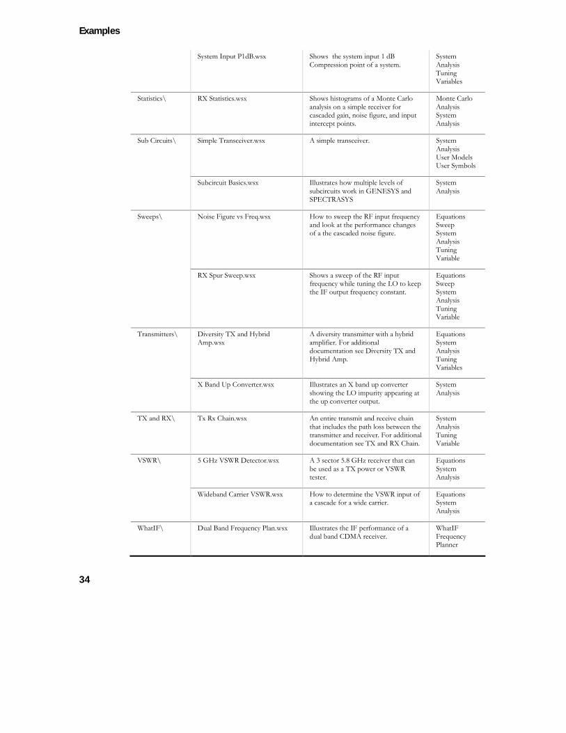
Statistics\ RX Statistics.wsx Shows histograms of a Monte Carlo analysis on a simple receiver for cascaded gain, noise figure, and input intercept points.
Monte Carlo Analysis System Analysis
Simple Transceiver.wsx A simple transceiver. System Analysis User Models User Symbols
Sub Circuits\
Subcircuit Basics.wsx Illustrates how multiple levels of subcircuits work in GENESYS and SPECTRASYS
System Analysis
Noise Figure vs Freq.wsx How to sweep the RF input frequency and look at the performance changes of a the cascaded noise figure.
Equations Sweep System Analysis Tuning Variable
Sweeps\
RX Spur Sweep.wsx Shows a sweep of the RF input frequency while tuning the LO to keep the IF output frequency constant.
Equations Sweep System Analysis Tuning Variable
Diversity TX and Hybrid Amp.wsx
A diversity transmitter with a hybrid amplifier. For additional documentation see Diversity TX and Hybrid Amp.
Equations System Analysis Tuning Variables
Transmitters\
X Band Up Converter.wsx Illustrates an X band up converter showing the LO impurity appearing at the up converter output.
System Analysis
TX and RX\ Tx Rx Chain.wsx An entire transmit and receive chain that includes the path loss between the transmitter and receiver. For additional documentation see TX and RX Chain.
System Analysis Tuning Variable
5 GHz VSWR Detector.wsx A 3 sector 5.8 GHz receiver that can be used as a TX power or VSWR tester.
Equations System Analysis
VSWR\
Wideband Carrier VSWR.wsx How to determine the VSWR input of a cascade for a wide carrier.
Equations System Analysis
WhatIF\ Dual Band Frequency Plan.wsx Illustrates the IF performance of a dual band CDMA receiver.
WhatIF Frequency Planner

categories
35
Examples
36
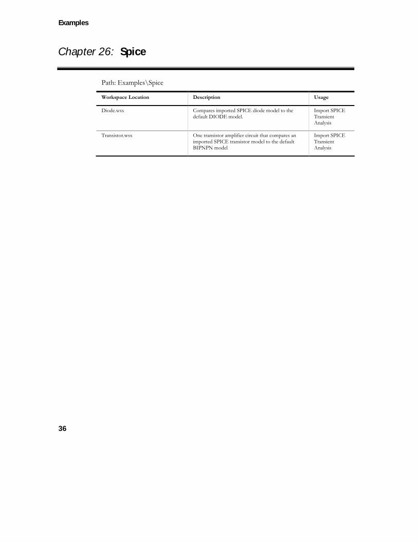
Chapter 26: Spice
Path: Examples\Spice
Workspace Location Description Usage
Diode.wsx Compares imported SPICE diode model to the default DIODE model.
Import SPICE Transient Analysis
Transistor.wsx One transistor amplifier circuit that compares an imported SPICE transistor model to the default BIPNPN model
Import SPICE Transient Analysis
categories
37
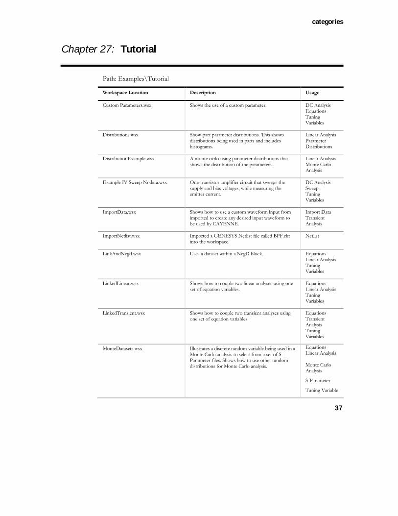
Chapter 27: Tutorial
Path: Examples\Tutorial
Workspace Location Description Usage
Custom Parameters.wsx Shows the use of a custom parameter. DC Analysis Equations Tuning Variables
Distributions.wsx Show part parameter distributions. This shows distributions being used in parts and includes histograms.
Linear Analysis Parameter Distributions
DistributionExample.wsx A monte carlo using parameter distributions that shows the distribution of the parameters.
Linear Analysis Monte Carlo Analysis
Example IV Sweep Nodata.wsx One-transistor amplifier circuit that sweeps the supply and bias voltages, while measuring the emitter current.
DC Analysis Sweep Tuning Variables
ImportData.wsx Shows how to use a custom waveform input from imported to create any desired input waveform to be used by CAYENNE.
Import Data Transient Analysis
ImportNetlist.wsx Imported a GENESYS Netlist file called BPF.ckt into the workspace.
Netlist
LinkAndNegd.wsx Uses a dataset within a NegD block. Equations Linear Analysis Tuning Variables
LinkedLinear.wsx Shows how to couple two linear analyses using one set of equation variables.
Equations Linear Analysis Tuning Variables
LinkedTransient.wsx Shows how to couple two transient analyses using one set of equation variables.
Equations Transient Analysis Tuning Variables
MonteDatasets.wsx Illustrates a discrete random variable being used in a Monte Carlo analysis to select from a set of S-Parameter files. Shows how to use other random distributions for Monte Carlo analysis.
Equations Linear Analysis Monte Carlo Analysis
S-Parameter
Tuning Variable
Examples
38
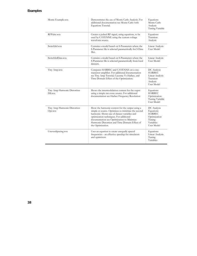
Monte Example.wsx Demonstrates the use of Monte Carlo Analysis. For additional documentation see Monte Carlo with Equations Tutorial.
Equations Monte Carlo Analysis Tuning Variable
RFPulse.wsx Creates a pulsed RF signal, using equations, to be used by CAYENNE using the custom voltage waveform source.
Equations Transient Analysis
SwitchSel.wsx Contains a model based on S-Parameters where the S-Parameter file is selected parametrically for S Data files.
Linear Analysis User Model
SwitchSelData.wsx Contains a model based on S-Parameters where the S-Parameter file is selected parametrically from local datasets.
Linear Analysis User Model
Tiny Amp.wsx Compares HARBEC and CAYENNE on a one-transistor amplifier. For additional documentation see Tiny Amp Tutorial, Cayenne Vs Harbec, and Time Domain Effect of the Optimization.
DC Analysis HARBEC Linear Analysis Transient Analysis User Model
Tiny Amp Harmonic Distortion IM.wsx
Shows the intermodulation content for the ouput using a simple two-tone source. For additional documentation see Harbec Frequency Resolution
Equations HARBEC Optimization Tuning Variable User Model
Tiny Amp Harmonic Distortion Opt.wsx
Show the harmonic content for the output using a simple cs source. Optimizes to minimize the second harmonic. Shows use of dataset variables and optimization techniques. For additional documentation see Optimization to Minimize Harmonic Distortion and Time Domain Effect of the Optimization.
DC Analysis Equations HARBEC Optimization Tuning Variables User Model
UnevenSpacing.wsx Uses an equation to create unequally spaced frequencies - an effective speedup for simulators and optimizers.
Equations Linear Analysis Tuning Variables

categories
39
Chapter 28: VerilogA
Path: Examples\VerilogA
Workspace Location Description Usage
PIN diode.wsx A resistor is modeled using the Verilog-A compiler and used in a diode model.
DC Analysis Equations HARBEC Linear Analysis Sweep Tuning Variables User Model
Examples
40
Chapter 29: VIEWER
Path: Examples\VIEWER
Workspace Location Description Usage
LNMIT3.wsx Multimode viewer data. Features visualization of multiconductor line eigenmodes.
EMPOWER Layout
METR16.wsx Simple line segment analysis to give a basic visualization. EMPOWER Layout
VIA.wsx Via-hole viewer. Features visualizations of X, Y, and Z components.
EMPOWER Layout
41
Chapter 30: Examples With Additional Documentation
AFILTER
Lowpass Minimum Inductor Examples\AFILTER\Lowpass Min L.wsx
Abstract
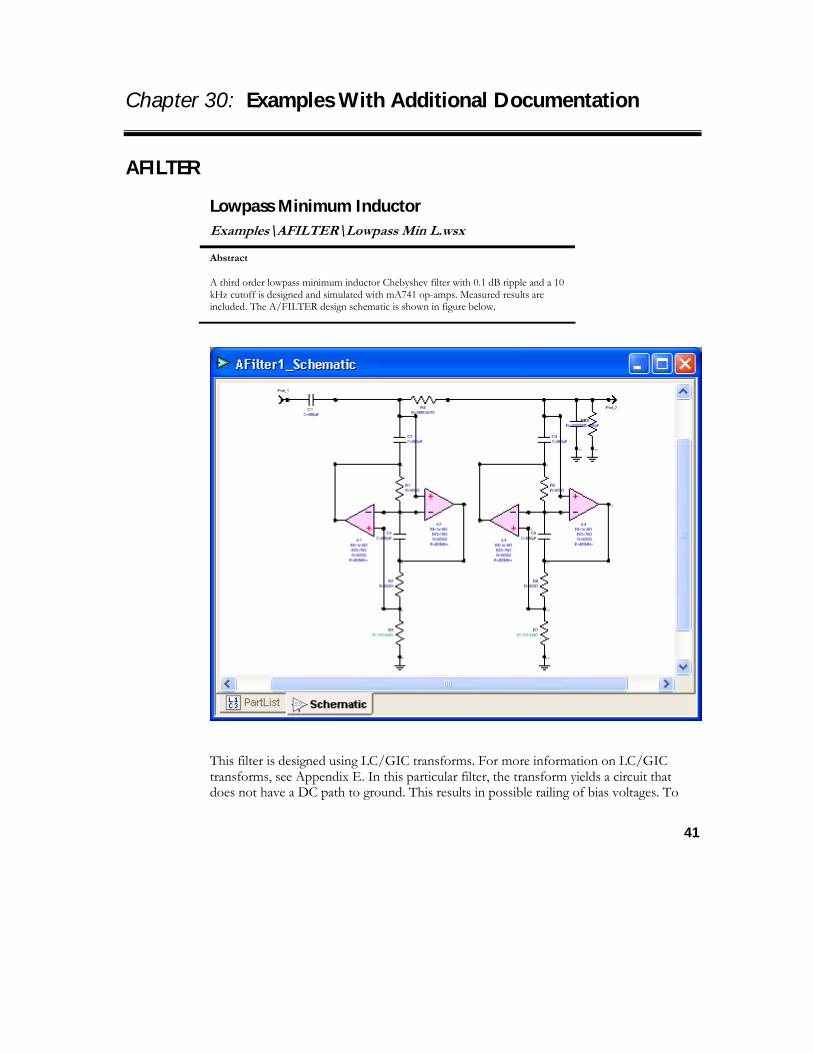
A third order lowpass minimum inductor Chebyshev filter with 0.1 dB ripple and a 10 kHz cutoff is designed and simulated with mA741 op-amps. Measured results are included. The A/FILTER design schematic is shown in figure below.
This filter is designed using LC/GIC transforms. For more information on LC/GIC transforms, see Appendix E. In this particular filter, the transform yields a circuit that does not have a DC path to ground. This results in possible railing of bias voltages. To

Examples
42
compensate, A/FILTER automatically includes a 100k resistor to ground at the output. This will work fine, as long as 100k is large compared to the impedance of the output capacitor within the filter passband. If it is not, the parallel combination of the shunt resistor and capacitor may cause a mismatch at the load. Therefore, if small valued capacitors must be used, the output resistor may need to be increased to restore the filter response.
There is an inherent loss of 6dB in this filter type. If your application requires no loss or requires gain, this can be achieved by the use of an output buffer. Output buffering is setup from the Setup menu, Preferences Window. Once enabled, the main A/FILTER window will have an input cell for gain to control the gain of the output buffer.
Tuning the grounded resistor in each “D element” (R3 and R7 in the schematic above) directly affects the cutoff frequency. The “D elements” are independent enough that usually only one resistor needs to be adjusted unless a wide tuning range is needed.
This type is very sensitive to op-amp bandwidth. With a 1 MHz bandwidth amplifier, a 10 kHz filter may start to experience rolloff prematurely. This can usually be fixed by optimization with Linear Analysis.
A/FILTER automatically writes an optimization block into the circuit or schematic file. Several components within each filter type are marked for tuning and/or optimization. These parts can be used to tune the filter response back if other components are set to standard values, or vary slightly due to tolerances. (This will be illustrated in "Lowpass Multiple Feedback" example)
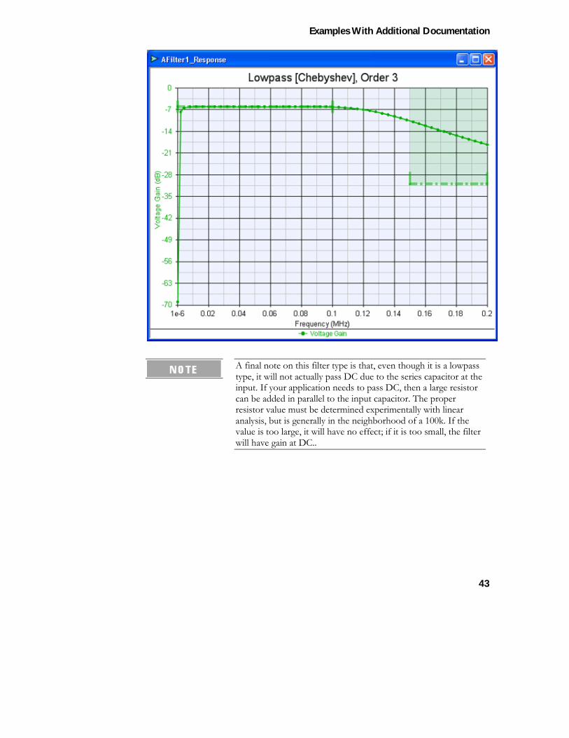
The following figure shows the predicted and measured responses. The circles show the response when using 347 op-amps (3 MHz bandwidth), while the triangles show the response when using mA741 op-amps (1 MHz bandwidth).
Examples With Additional Documentation
43
A final note on this filter type is that, even though it is a lowpass type, it will not actually pass DC due to the series capacitor at the input. If your application needs to pass DC, then a large resistor can be added in parallel to the input capacitor. The proper resistor value must be determined experimentally with linear analysis, but is generally in the neighborhood of a 100k. If the value is too large, it will have no effect; if it is too small, the filter will have gain at DC..
Examples
44
Lowpass Minimum Capacitor Examples\AFILTER\Lowpass Min C.wsx
Abstract
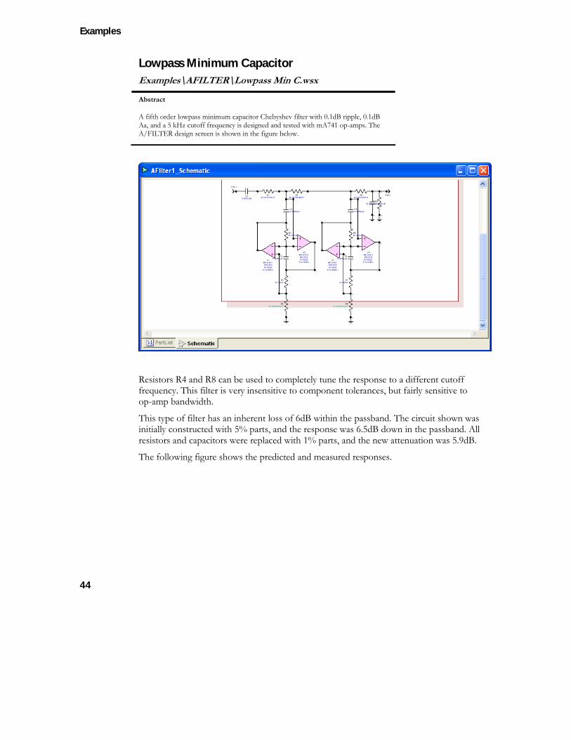
A fifth order lowpass minimum capacitor Chebyshev filter with 0.1dB ripple, 0.1dB Aa, and a 5 kHz cutoff frequency is designed and tested with mA741 op-amps. The A/FILTER design screen is shown in the figure below.
Resistors R4 and R8 can be used to completely tune the response to a different cutoff frequency. This filter is very insensitive to component tolerances, but fairly sensitive to op-amp bandwidth.
This type of filter has an inherent loss of 6dB within the passband. The circuit shown was initially constructed with 5% parts, and the response was 6.5dB down in the passband. All resistors and capacitors were replaced with 1% parts, and the new attenuation was 5.9dB.
The following figure shows the predicted and measured responses.
Examples With Additional Documentation
45
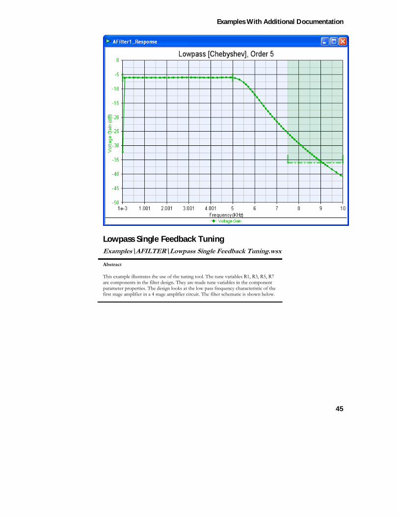
Lowpass Single Feedback Tuning Examples\AFILTER\Lowpass Single Feedback Tuning.wsx
Abstract
This example illustrates the use of the tuning tool. The tune variables R1, R3, R5, R7 are components in the filter design. They are made tune variables in the component parameter properties. The design looks at the low pass frequency characteristic of the first stage amplifier in a 4 stage amplifier circuit. The filter schematic is shown below.
Examples
46
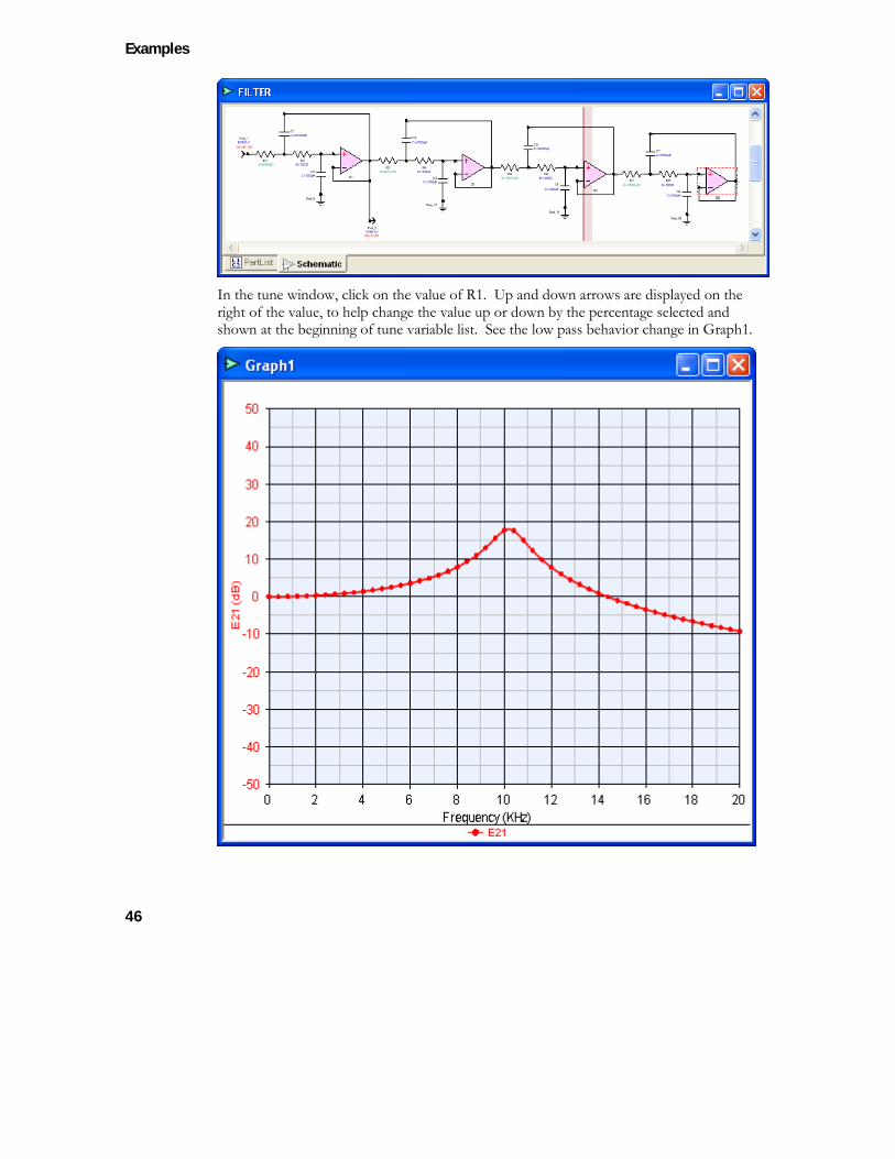
In the tune window, click on the value of R1. Up and down arrows are displayed on the right of the value, to help change the value up or down by the percentage selected and shown at the beginning of tune variable list. See the low pass behavior change in Graph1.
Examples With Additional Documentation
47
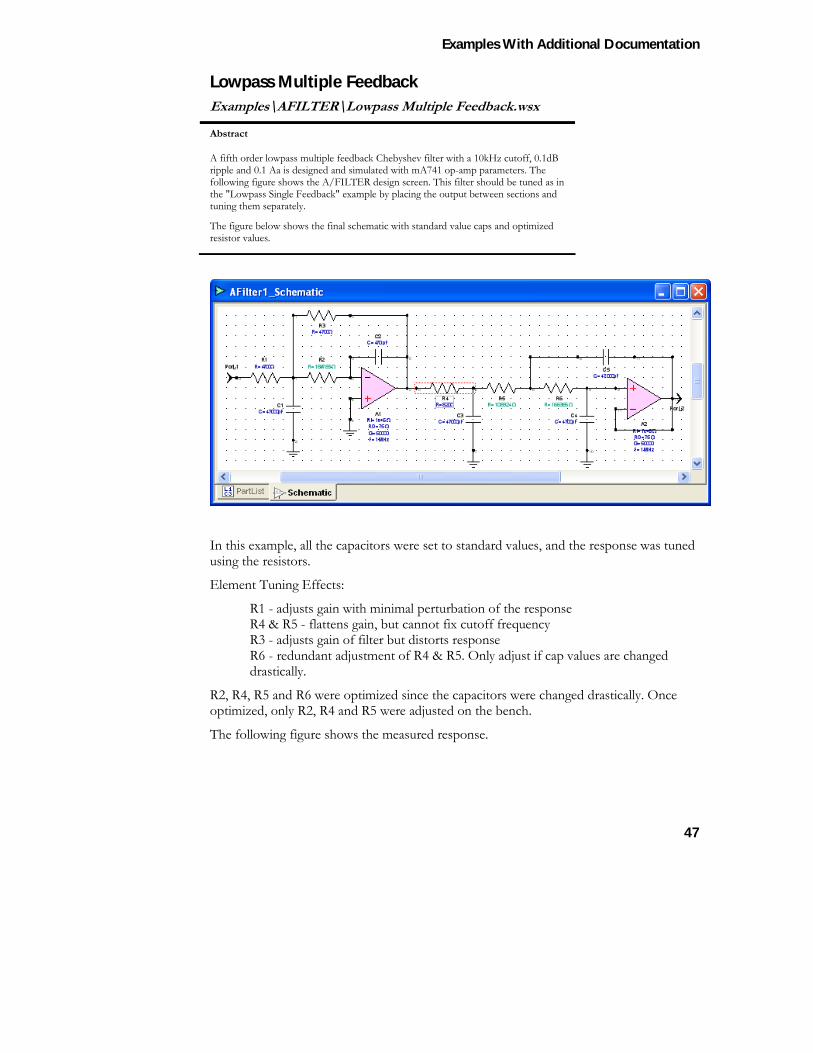
Lowpass Multiple Feedback Examples\AFILTER\Lowpass Multiple Feedback.wsx
Abstract
A fifth order lowpass multiple feedback Chebyshev filter with a 10kHz cutoff, 0.1dB ripple and 0.1 Aa is designed and simulated with mA741 op-amp parameters. The following figure shows the A/FILTER design screen. This filter should be tuned as in the "Lowpass Single Feedback" example by placing the output between sections and tuning them separately.
The figure below shows the final schematic with standard value caps and optimized resistor values.
In this example, all the capacitors were set to standard values, and the response was tuned using the resistors.
Element Tuning Effects:
R1 - adjusts gain with minimal perturbation of the response R4 & R5 - flattens gain, but cannot fix cutoff frequency R3 - adjusts gain of filter but distorts response R6 - redundant adjustment of R4 & R5. Only adjust if cap values are changed drastically.
R2, R4, R5 and R6 were optimized since the capacitors were changed drastically. Once optimized, only R2, R4 and R5 were adjusted on the bench.
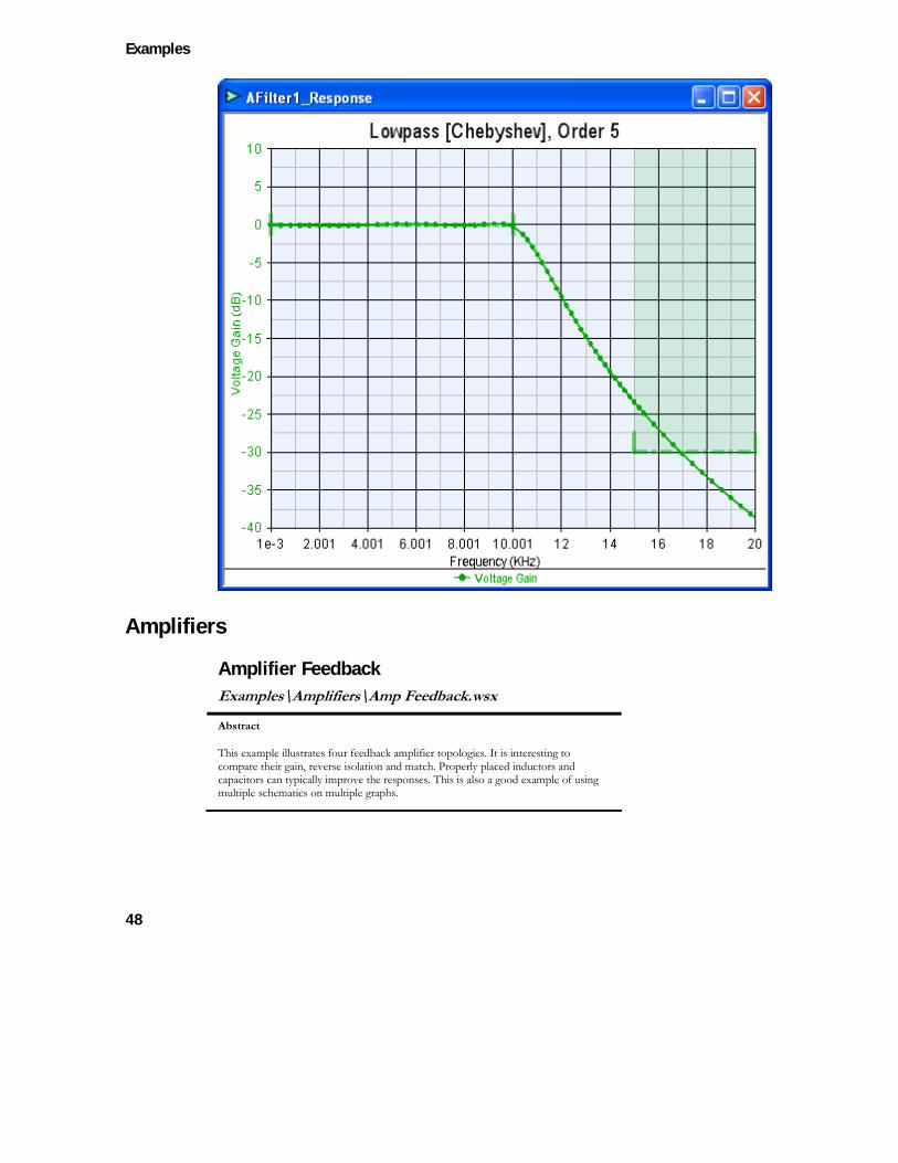
The following figure shows the measured response.
Examples
48
Amplifiers
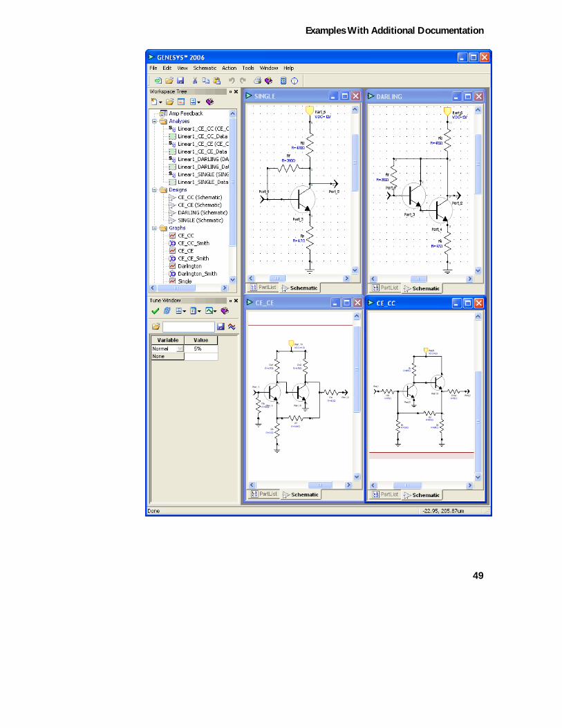
Amplifier Feedback Examples\Amplifiers\Amp Feedback.wsx
Abstract
This example illustrates four feedback amplifier topologies. It is interesting to compare their gain, reverse isolation and match. Properly placed inductors and capacitors can typically improve the responses. This is also a good example of using multiple schematics on multiple graphs.
Examples With Additional Documentation
49
Examples
50
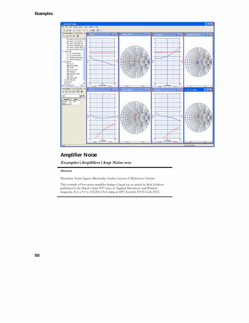
Amplifier Noise Examples\Amplifiers\Amp Noise.wsx
Abstract
Illustrates: Noise Figure, Microstrip, Circles, Layout of Microwave Circuits
This example of low-noise amplifier design is based on an article by Rob Lefebvre published in the March/April 1997 issue of Applied Microwave and Wireless magazine. It is a 9.5 to 10 GHz LNA using an HP/Avantek 10135 GaAs FET.
Examples With Additional Documentation
51
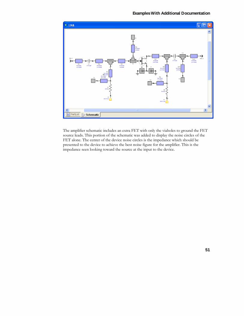
The amplifier schematic includes an extra FET with only the viaholes to ground the FET source leads. This portion of the schematic was added to display the noise circles of the FET alone. The center of the device noise circles is the impedance which should be presented to the device to achieve the best noise figure for the amplifier. This is the impedance seen looking toward the source at the input to the device.
Examples
52
Examples With Additional Documentation
53
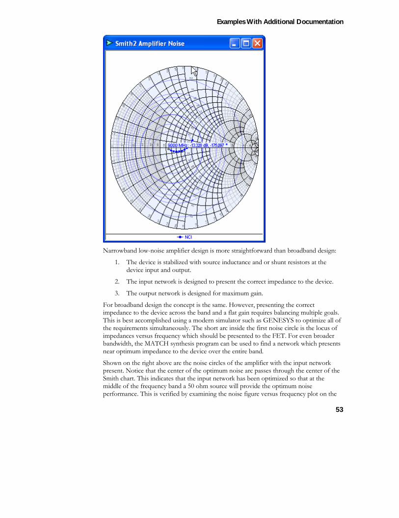
Narrowband low-noise amplifier design is more straightforward than broadband design:
1. The device is stabilized with source inductance and or shunt resistors at the device input and output.
2. The input network is designed to present the correct impedance to the device.
3. The output network is designed for maximum gain.
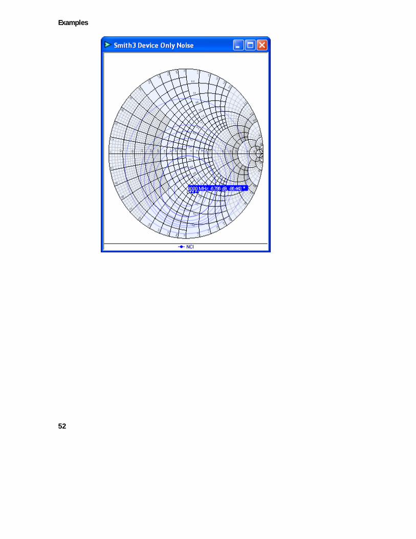
For broadband design the concept is the same. However, presenting the correct impedance to the device across the band and a flat gain requires balancing multiple goals. This is best accomplished using a modern simulator such as GENESYS to optimize all of the requirements simultaneously. The short arc inside the first noise circle is the locus of impedances versus frequency which should be presented to the FET. For even broader bandwidth, the MATCH synthesis program can be used to find a network which presents near optimum impedance to the device over the entire band.
Shown on the right above are the noise circles of the amplifier with the input network present. Notice that the center of the optimum noise arc passes through the center of the Smith chart. This indicates that the input network has been optimized so that at the middle of the frequency band a 50 ohm source will provide the optimum noise performance. This is verified by examining the noise figure versus frequency plot on the
Examples
54
left. The gain flatness was achieved by optimization of the output matching network. Better output return loss could have been achieved by optimizing for match instead of gain flatness. The match at the input falls where it must because the input network is optimized for best noise and not best match.
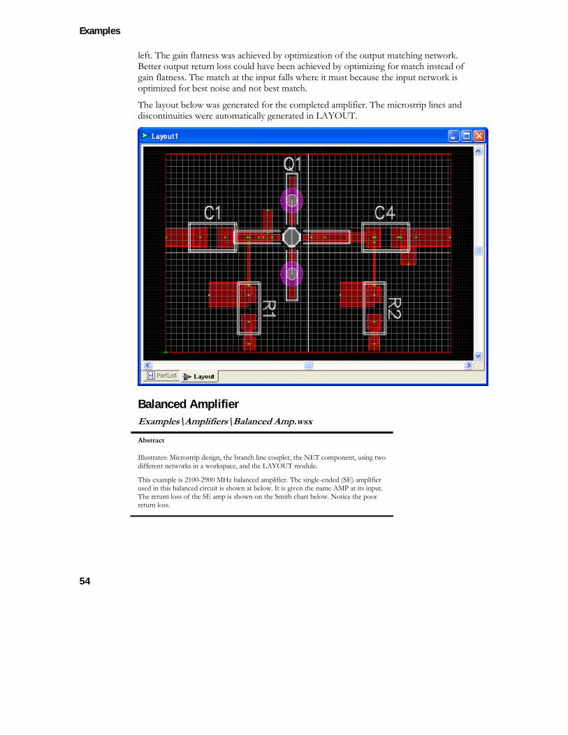
The layout below was generated for the completed amplifier. The microstrip lines and discontinuities were automatically generated in LAYOUT.
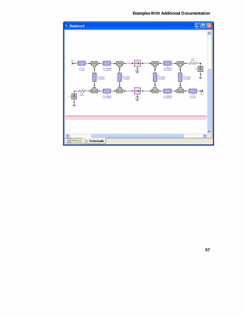
Balanced Amplifier Examples\Amplifiers\Balanced Amp.wsx
Abstract
Illustrates: Microstrip design, the branch line coupler, the NET component, using two different networks in a workspace, and the LAYOUT module.
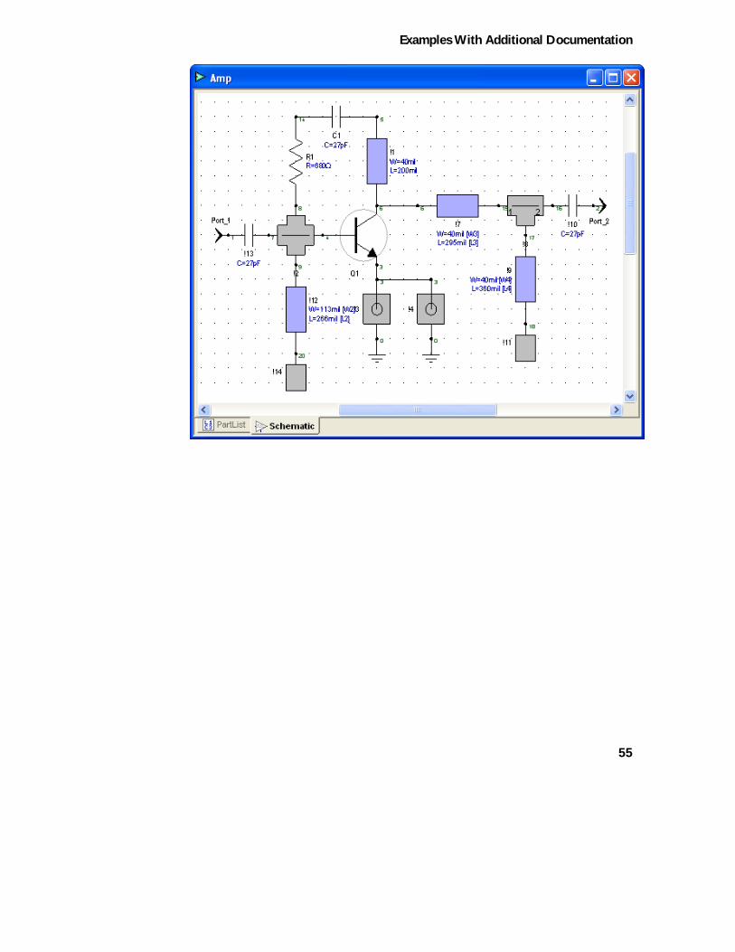
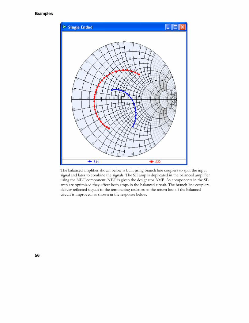
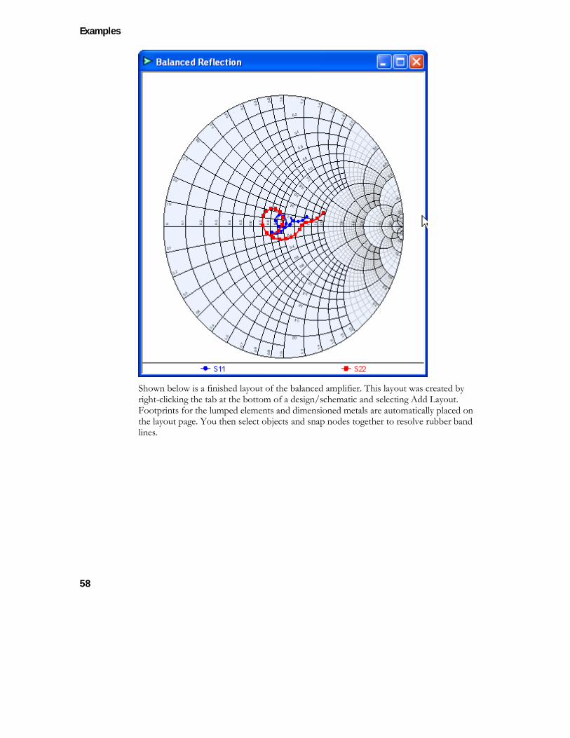
This example is 2100-2900 MHz balanced amplifier. The single-ended (SE) amplifier used in this balanced circuit is shown at below. It is given the name AMP at its input. The return loss of the SE amp is shown on the Smith chart below. Notice the poor return loss.
Examples With Additional Documentation
55
Examples
56
The balanced amplifier shown below is built using branch line couplers to split the input signal and later to combine the signals. The SE amp is duplicated in the balanced amplifier using the NET component. NET is given the designator AMP. As components in the SE amp are optimized they effect both amps in the balanced circuit. The branch line couplers deliver reflected signals to the terminating resistors so the return loss of the balanced circuit is improved, as shown in the response below.
Examples With Additional Documentation
57
Examples
58
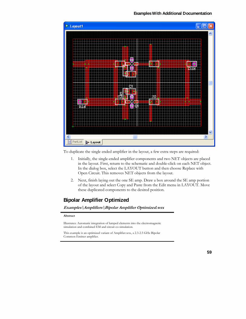
Shown below is a finished layout of the balanced amplifier. This layout was created by right-clicking the tab at the bottom of a design/schematic and selecting Add Layout. Footprints for the lumped elements and dimensioned metals are automatically placed on the layout page. You then select objects and snap nodes together to resolve rubber band lines.
Examples With Additional Documentation
59
To duplicate the single ended amplifier in the layout, a few extra steps are required:
1. Initially, the single-ended amplifier components and two NET objects are placed in the layout. First, return to the schematic and double-click on each NET object. In the dialog box, select the LAYOUT button and then choose Replace with Open Circuit. This removes NET objects from the layout.
2. Next, finish laying out the one SE amp. Draw a box around the SE amp portion of the layout and select Copy and Paste from the Edit menu in LAYOUT. Move these duplicated components to the desired position.
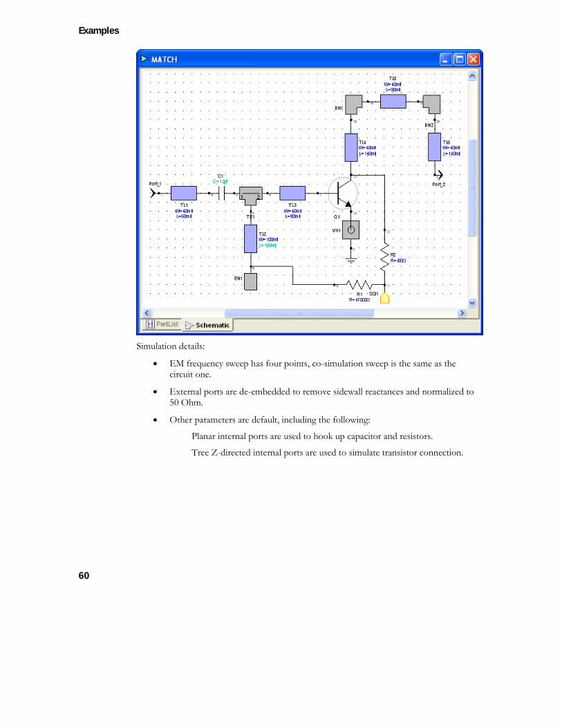
Bipolar Amplifier Optimized Examples\Amplifiers\Bipolar Amplifier Optimized.wsx
Abstract
Illustrates: Automatic integration of lumped elements into the electromagnetic simulation and combined EM and circuit co-simulation.
This example is an optimized variant of Amplifier.wsx, a 2.3-2.5 GHz Bipolar Common Emitter amplifier.
Examples
60
Simulation details:
• EM frequency sweep has four points, co-simulation sweep is the same as the circuit one.
• External ports are de-embedded to remove sidewall reactances and normalized to 50 Ohm.
• Other parameters are default, including the following:
Planar internal ports are used to hook up capacitor and resistors.
Tree Z-directed internal ports are used to simulate transistor connection.
Examples With Additional Documentation
61
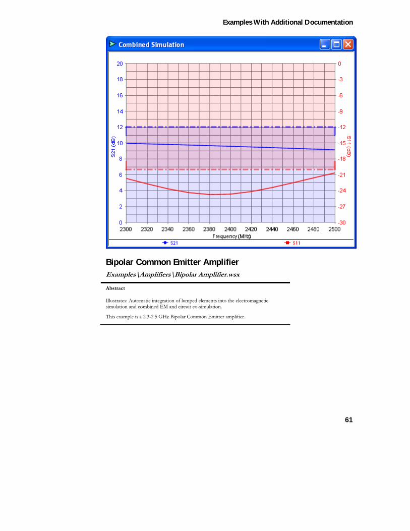
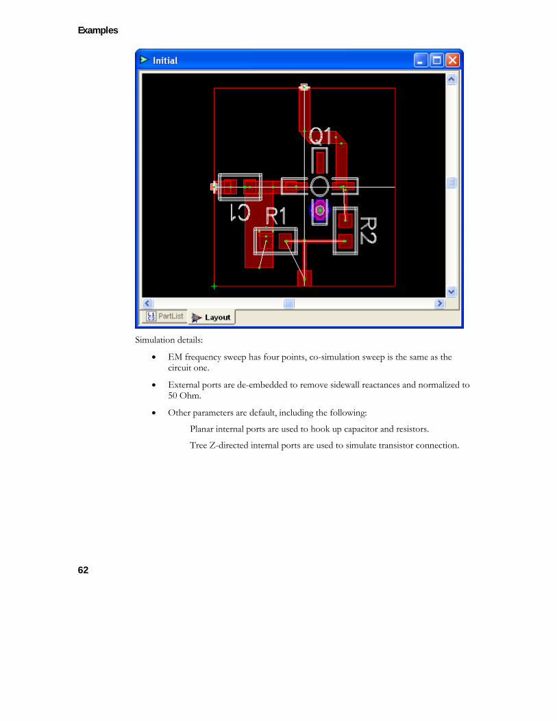
Bipolar Common Emitter Amplifier Examples\Amplifiers\Bipolar Amplifier.wsx
Abstract
Illustrates: Automatic integration of lumped elements into the electromagnetic simulation and combined EM and circuit co-simulation.
This example is a 2.3-2.5 GHz Bipolar Common Emitter amplifier.
Examples
62
Simulation details:
• EM frequency sweep has four points, co-simulation sweep is the same as the circuit one.
• External ports are de-embedded to remove sidewall reactances and normalized to 50 Ohm.
• Other parameters are default, including the following:
Planar internal ports are used to hook up capacitor and resistors.
Tree Z-directed internal ports are used to simulate transistor connection.
Examples With Additional Documentation
63
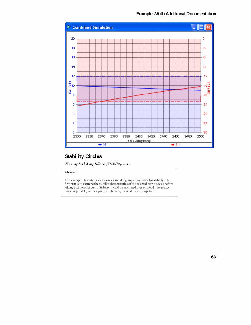
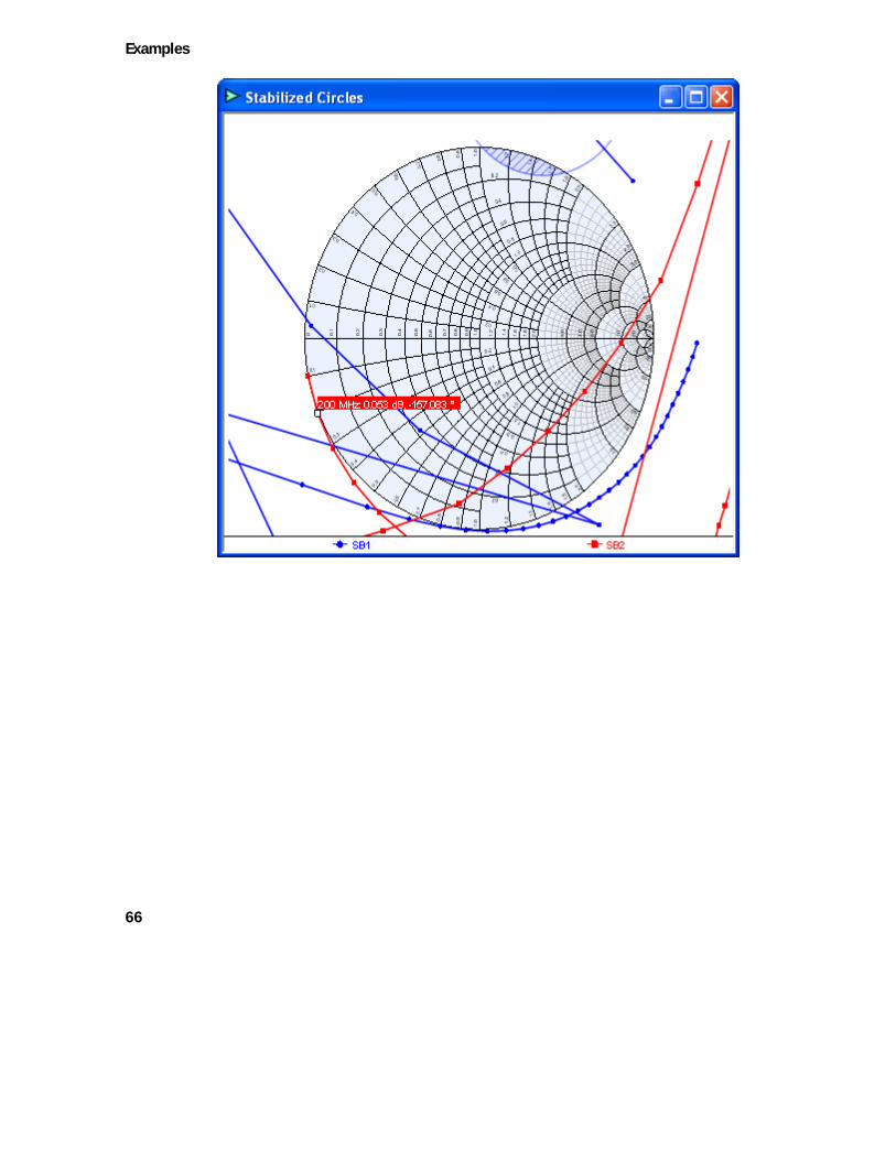
Stability Circles Examples\Amplifiers\Stability.wsx
Abstract
This example illustrates stability circles and designing an amplifier for stability. The first step is to examine the stability characteristics of the selected active device before adding additional circuitry. Stability should be examined over as broad a frequency range as possible, and not just over the range desired for the amplifier.
Examples
64
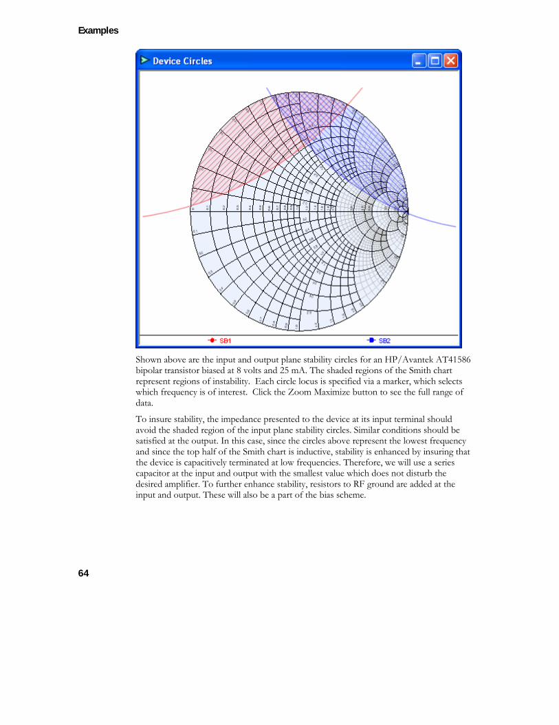
Shown above are the input and output plane stability circles for an HP/Avantek AT41586 bipolar transistor biased at 8 volts and 25 mA. The shaded regions of the Smith chart represent regions of instability. Each circle locus is specified via a marker, which selects which frequency is of interest. Click the Zoom Maximize button to see the full range of data.
To insure stability, the impedance presented to the device at its input terminal should avoid the shaded region of the input plane stability circles. Similar conditions should be satisfied at the output. In this case, since the circles above represent the lowest frequency and since the top half of the Smith chart is inductive, stability is enhanced by insuring that the device is capacitively terminated at low frequencies. Therefore, we will use a series capacitor at the input and output with the smallest value which does not disturb the desired amplifier. To further enhance stability, resistors to RF ground are added at the input and output. These will also be a part of the bias scheme.
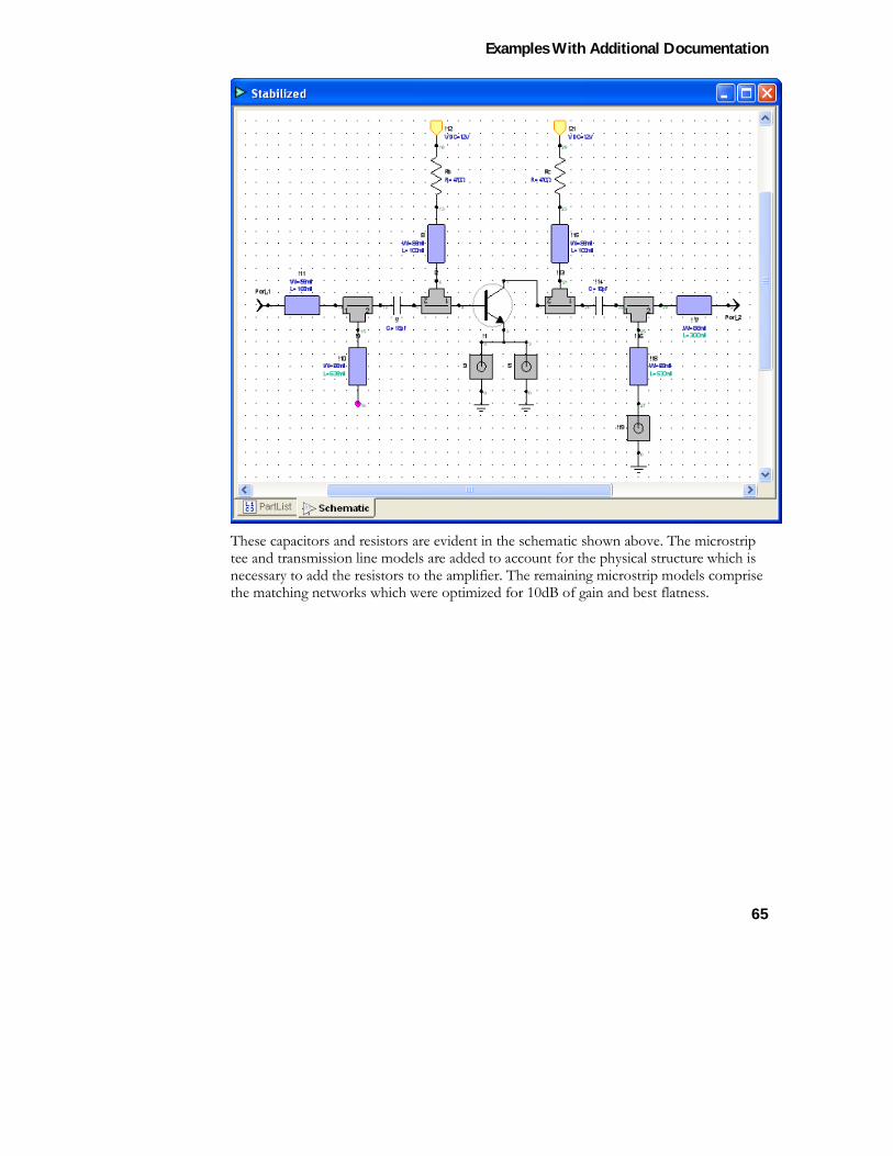
Examples With Additional Documentation
65
These capacitors and resistors are evident in the schematic shown above. The microstrip tee and transmission line models are added to account for the physical structure which is necessary to add the resistors to the amplifier. The remaining microstrip models comprise the matching networks which were optimized for 10dB of gain and best flatness.
Examples
66
Examples With Additional Documentation
67
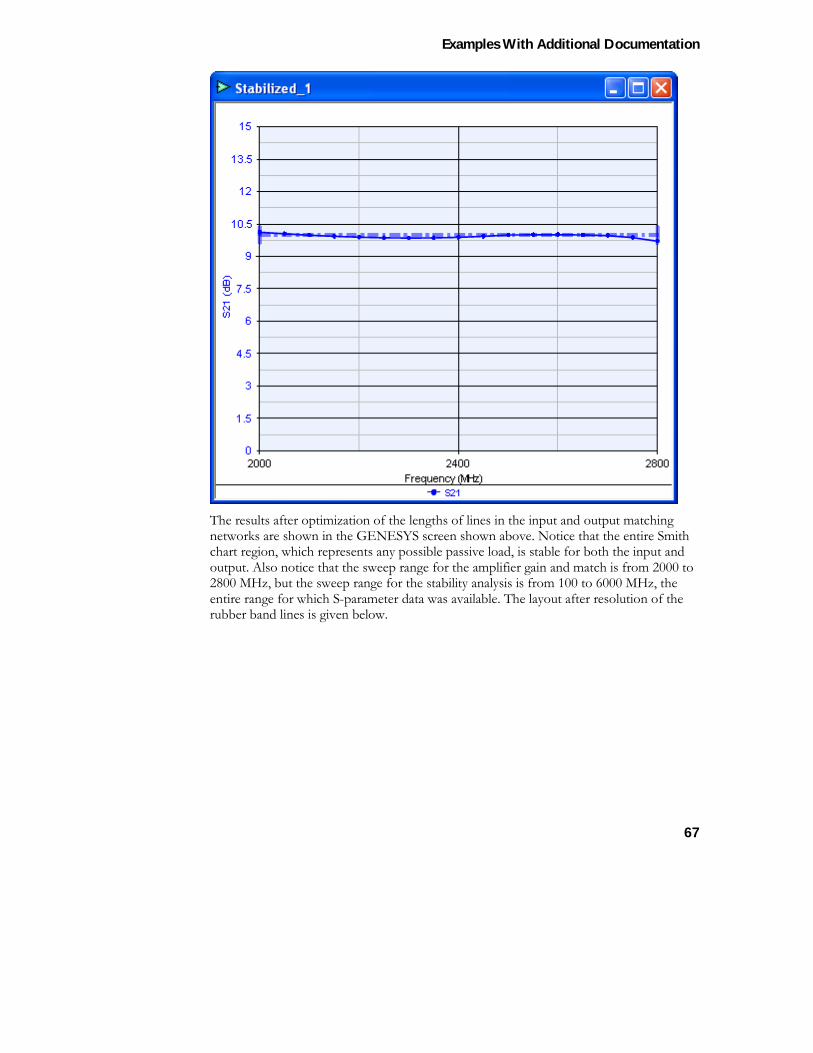
The results after optimization of the lengths of lines in the input and output matching networks are shown in the GENESYS screen shown above. Notice that the entire Smith chart region, which represents any possible passive load, is stable for both the input and output. Also notice that the sweep range for the amplifier gain and match is from 2000 to 2800 MHz, but the sweep range for the stability analysis is from 100 to 6000 MHz, the entire range for which S-parameter data was available. The layout after resolution of the rubber band lines is given below.
Examples
68
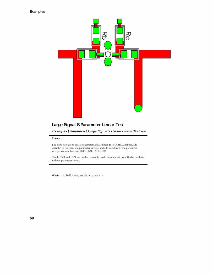
Large Signal S Parameter Linear Test Examples\Amplifiers\Large Signal S Param Linear Test.wsx
Abstract
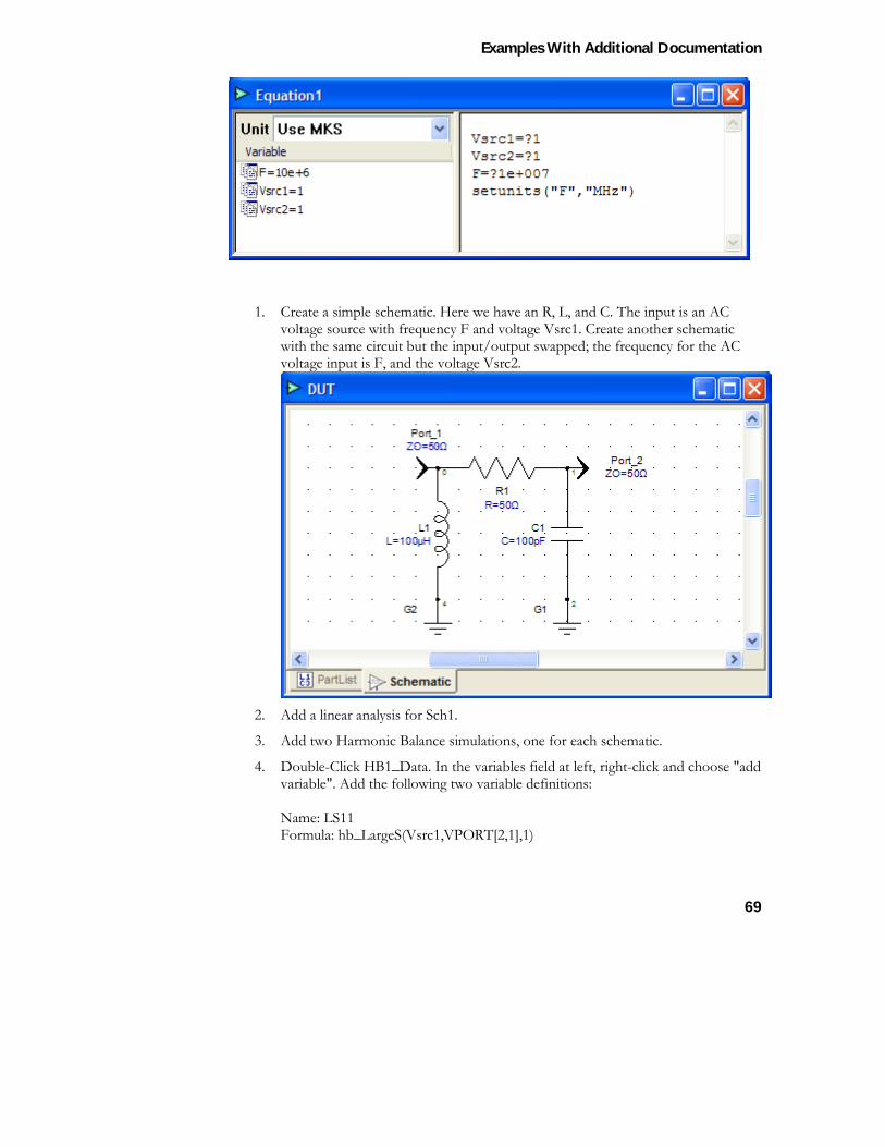
The steps here are to create schematics, create linear & HARBEC analyses, add variables to the data, add parameter sweeps, and add variables to the parameter sweeps. We can thus find LS11, LS21, LS12, LS22. If only LS11 and LS21 are needed, you only need one schematic, one Harbec analysis and one parameter sweep.
Write the following in the equations:
Examples With Additional Documentation
69
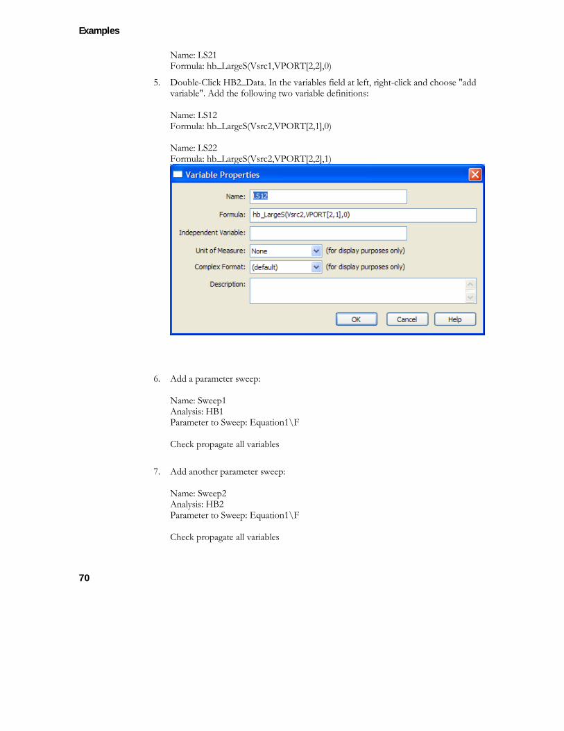
1. Create a simple schematic. Here we have an R, L, and C. The input is an AC voltage source with frequency F and voltage Vsrc1. Create another schematic with the same circuit but the input/output swapped; the frequency for the AC voltage input is F, and the voltage Vsrc2.
2. Add a linear analysis for Sch1.
3. Add two Harmonic Balance simulations, one for each schematic.
4. Double-Click HB1_Data. In the variables field at left, right-click and choose "add variable". Add the following two variable definitions: Name: LS11 Formula: hb_LargeS(Vsrc1,VPORT[2,1],1)
Examples
70
Name: LS21 Formula: hb_LargeS(Vsrc1,VPORT[2,2],0)
5. Double-Click HB2_Data. In the variables field at left, right-click and choose "add variable". Add the following two variable definitions: Name: LS12 Formula: hb_LargeS(Vsrc2,VPORT[2,1],0) Name: LS22 Formula: hb_LargeS(Vsrc2,VPORT[2,2],1)
6. Add a parameter sweep: Name: Sweep1 Analysis: HB1 Parameter to Sweep: Equation1\F Check propagate all variables
7. Add another parameter sweep: Name: Sweep2 Analysis: HB2 Parameter to Sweep: Equation1\F Check propagate all variables
Examples With Additional Documentation
71
8. Make sure all the simulations are up to date and you will see data that match the S-parameters exactly since these are all linear components. The table in the workspace compares LSij with Sij.
Antennas
Agile Antenna Examples\Antennas\Agile Antenna.wsx
Abstract
A microstrip patch antenna loaded with two varactor diodes.
Illustrates: combined EM and circuit theory simulation of a frequency agile antenna, manual connection of lumped element in EMPOWER, comparison with measured data.
Examples
72
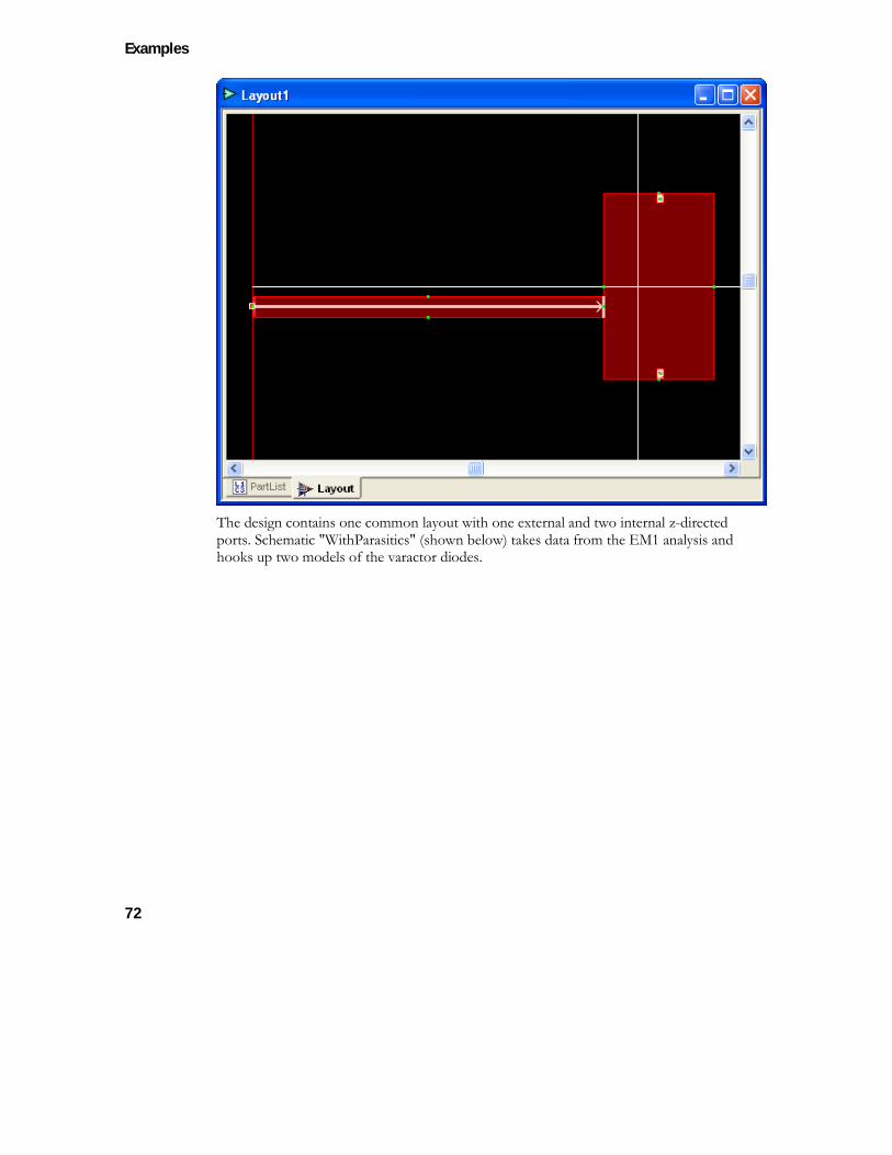
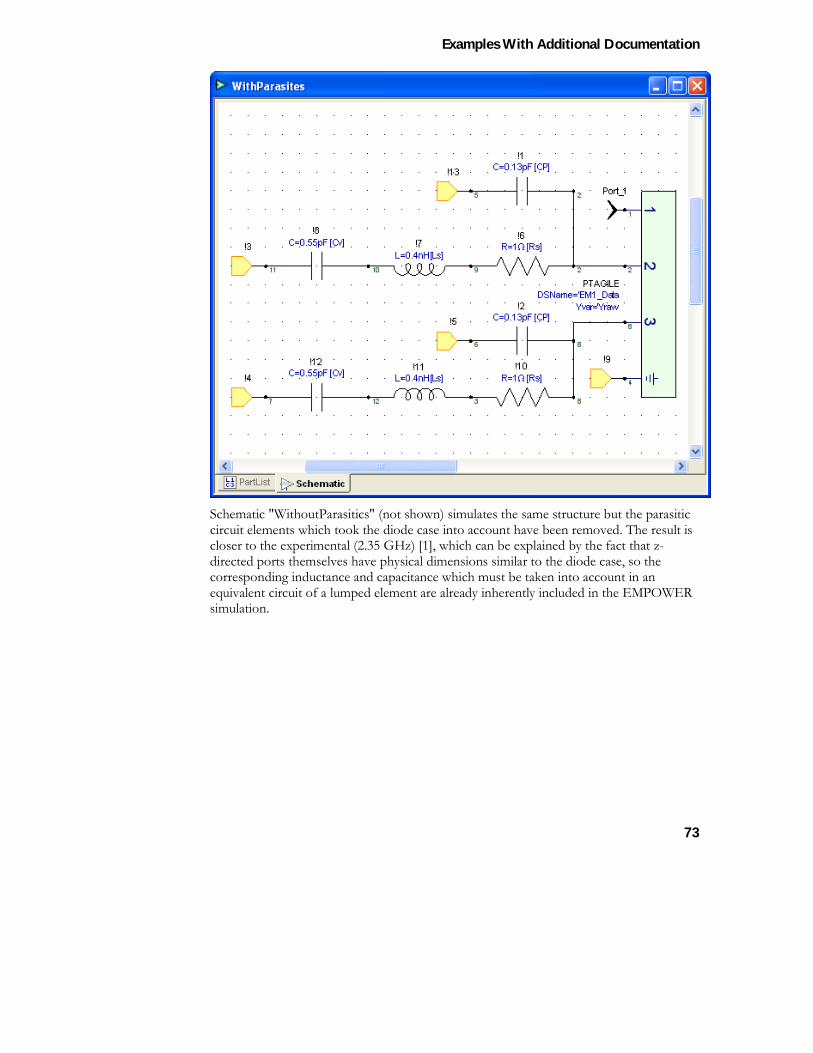
The design contains one common layout with one external and two internal z-directed ports. Schematic "WithParasitics" (shown below) takes data from the EM1 analysis and hooks up two models of the varactor diodes.
Examples With Additional Documentation
73
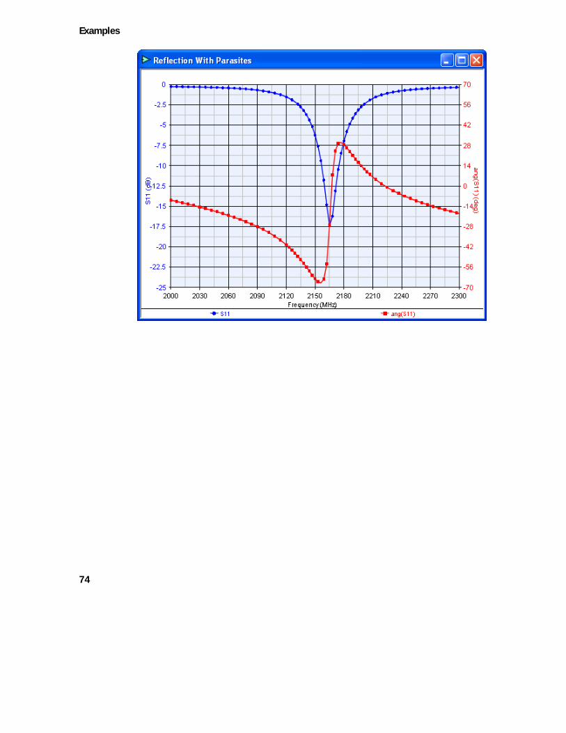
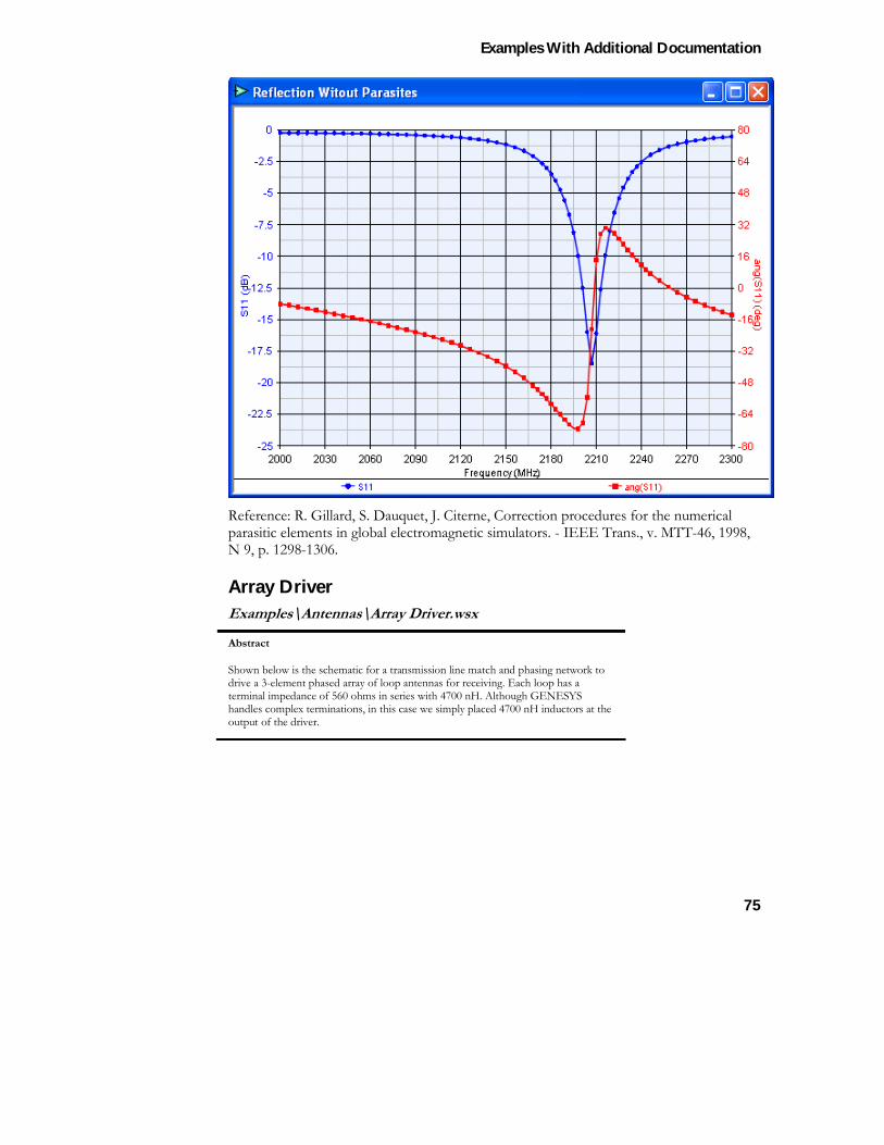
Schematic "WithoutParasitics" (not shown) simulates the same structure but the parasitic circuit elements which took the diode case into account have been removed. The result is closer to the experimental (2.35 GHz) [1], which can be explained by the fact that z-directed ports themselves have physical dimensions similar to the diode case, so the corresponding inductance and capacitance which must be taken into account in an equivalent circuit of a lumped element are already inherently included in the EMPOWER simulation.
Examples
74
Examples With Additional Documentation
75
Reference: R. Gillard, S. Dauquet, J. Citerne, Correction procedures for the numerical parasitic elements in global electromagnetic simulators. - IEEE Trans., v. MTT-46, 1998, N 9, p. 1298-1306.
Array Driver Examples\Antennas\Array Driver.wsx
Abstract
Shown below is the schematic for a transmission line match and phasing network to drive a 3-element phased array of loop antennas for receiving. Each loop has a terminal impedance of 560 ohms in series with 4700 nH. Although GENESYS handles complex terminations, in this case we simply placed 4700 nH inductors at the output of the driver.
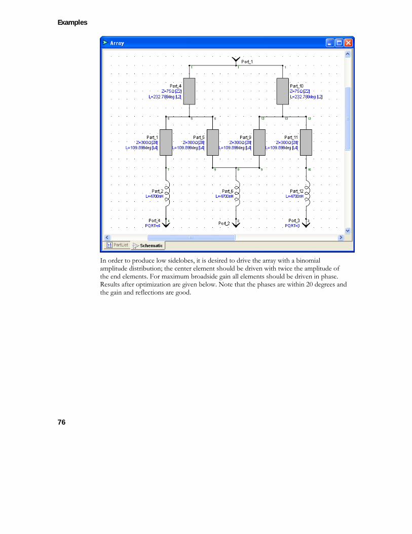
Examples
76
In order to produce low sidelobes, it is desired to drive the array with a binomial amplitude distribution; the center element should be driven with twice the amplitude of the end elements. For maximum broadside gain all elements should be driven in phase. Results after optimization are given below. Note that the phases are within 20 degrees and the gain and reflections are good.
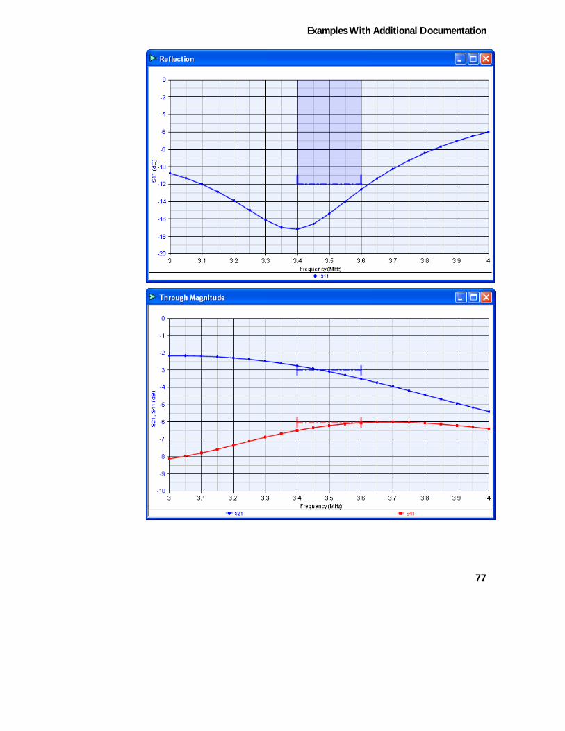
Examples With Additional Documentation
77
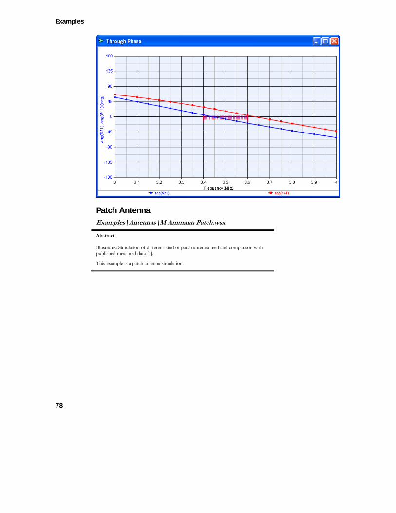
Examples
78
Patch Antenna Examples\Antennas\M Ammann Patch.wsx
Abstract
Illustrates: Simulation of different kind of patch antenna feed and comparison with published measured data [1].
This example is a patch antenna simulation.
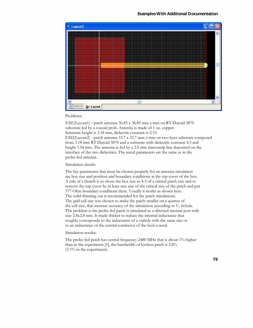
Examples With Additional Documentation
79
Problems: EM1(Layout1) - patch antenna 36.85 x 36.85 mm x mm on RT Duroid 5870 substrate fed by a coaxial prob. Antenna is made of 1 oz. copper. Substrate height is 3.18 mm, dielectric constant is 2.33. EM2(Layout2) - patch antenna 33.7 x 33.7 mm x mm on two layer substrate composed from 3.18 mm RT Duroid 5870 and a substrate with dielectric constant 4.5 and height 1.54 mm. The antenna is fed by a 2.9 mm microstrip line deposited on the interface of the two dielectrics. The metal parameters are the same as in the probe-fed antenna.
Simulation details: The key parameters that must be chosen properly for an antenna simulation are box size and position and boundary conditions at the top cover of the box. A rule of a thumb is to chose the box size as 4-5 of a critical patch size and to remove the top cover by at least one size of the critical size of the patch and put 377 Ohm boundary conditions there. Usually it works as shown here. The solid thinning out is recommended for the patch simulations. The grid cell size was chosen to make the patch smaller on a quarter of the cell size, that increase accuracy of the simulation according to U. Schulz. The problem is the probe-fed patch is simulated as z-directed internal port with size 2.8x2.8 mm. It made thicker to reduce the internal inductance that roughly corresponds to the inductance of a viahole with the same size or to an inductance of the central conductor of the feed coaxial.
Simulation results: The probe-fed patch has central frequency 2480 MHz that is about 1% higher than in the experiment [1], the bandwidth of lossless patch is 2.8% (3.1% in the experiment).
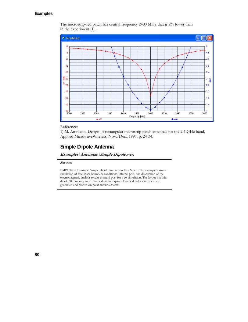
Examples
80
The microstrip-fed patch has central frequency 2400 MHz that is 2% lower than in the experiment [1].
Reference: 1) M. Ammann, Design of rectangular microstrip patch antennas for the 2.4 GHz band, Applied MicrowaveWireless, Nov./Dec., 1997, p. 24-34.
Simple Dipole Antenna Examples\Antennas\Simple Dipole.wsx
Abstract
EMPOWER Example: Simple Dipole Antenna in Free Space. This example features simulation of free-space boundary conditions, internal port, and description of the electromagnetic analysis results as multi-port for a co-simulation. The layout is a thin dipole 58 mm long and 1 mm wide in free space. Far-field radiation data is also generated and plotted on polar antenna charts.
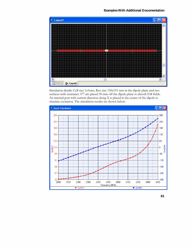
Examples With Additional Documentation
81
Simulation details: Cell size 1x1mm, Box size 150x151 mm in the dipole plane and two surfaces with resistance 377 are placed 50 mm off the dipole plane to absorb EM fields. An internal port with current direction along X is placed in the center of the dipole to simulate excitation. The simulation results are shown below:
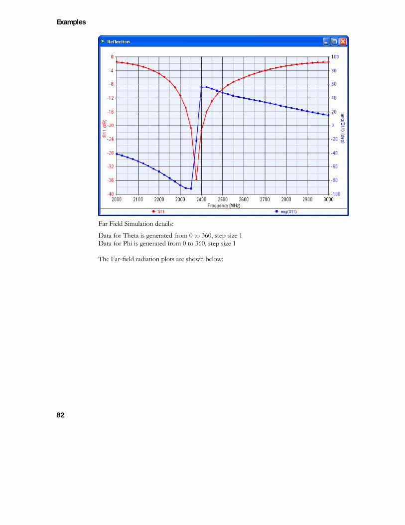
Examples
82
Far Field Simulation details:
Data for Theta is generated from 0 to 360, step size 1 Data for Phi is generated from 0 to 360, step size 1 The Far-field radiation plots are shown below:
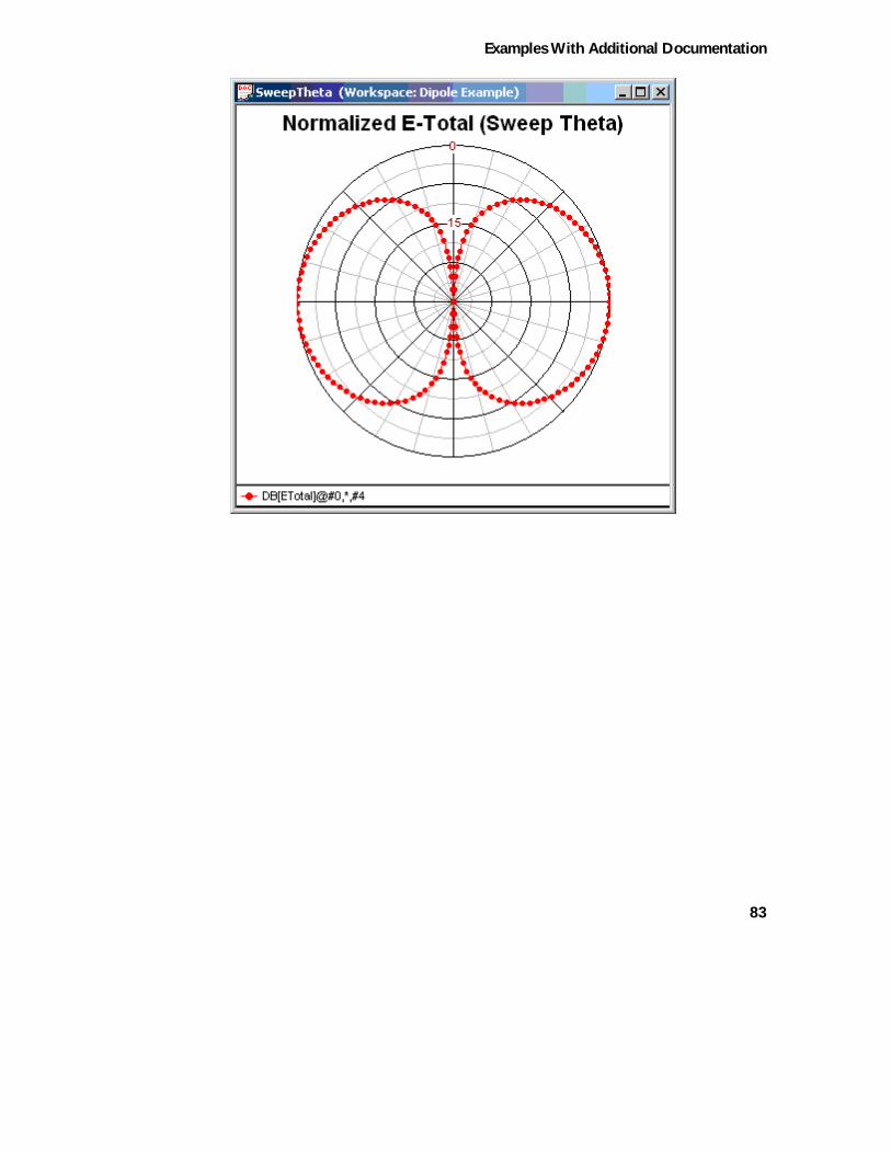
Examples With Additional Documentation
83
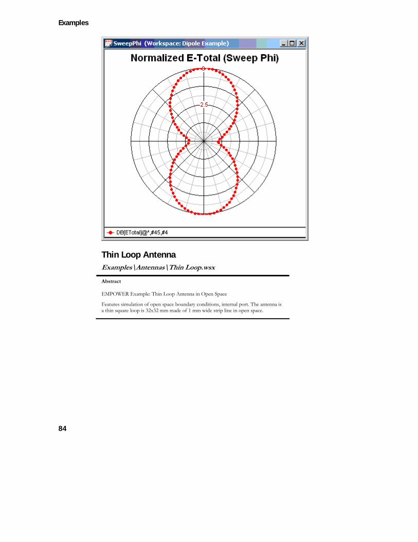
Examples
84
Thin Loop Antenna Examples\Antennas\Thin Loop.wsx
Abstract
EMPOWER Example: Thin Loop Antenna in Open Space
Features simulation of open space boundary conditions, internal port. The antenna is a thin square loop is 32x32 mm made of 1 mm wide strip line in open space.
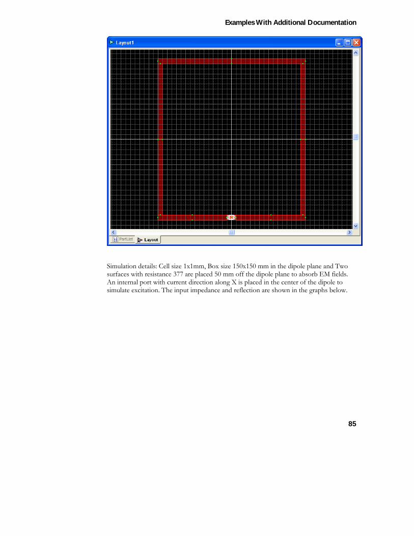
Examples With Additional Documentation
85
Simulation details: Cell size 1x1mm, Box size 150x150 mm in the dipole plane and Two surfaces with resistance 377 are placed 50 mm off the dipole plane to absorb EM fields. An internal port with current direction along X is placed in the center of the dipole to simulate excitation. The input impedance and reflection are shown in the graphs below.
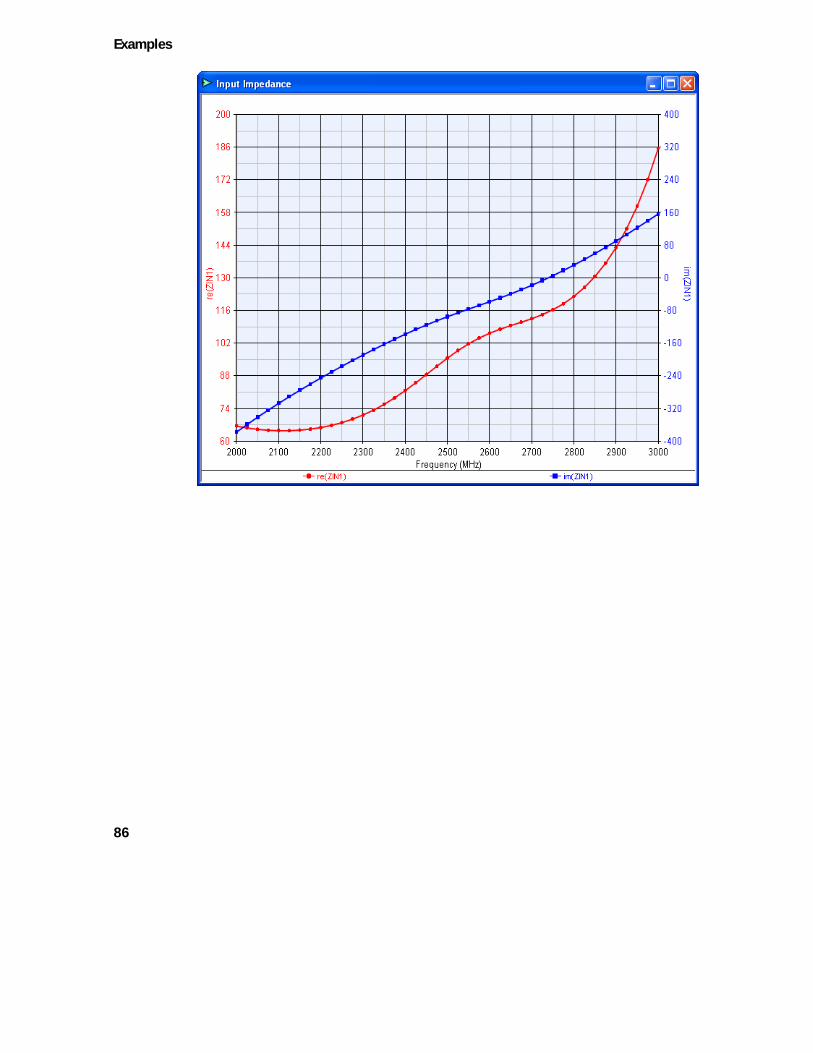
Examples
86
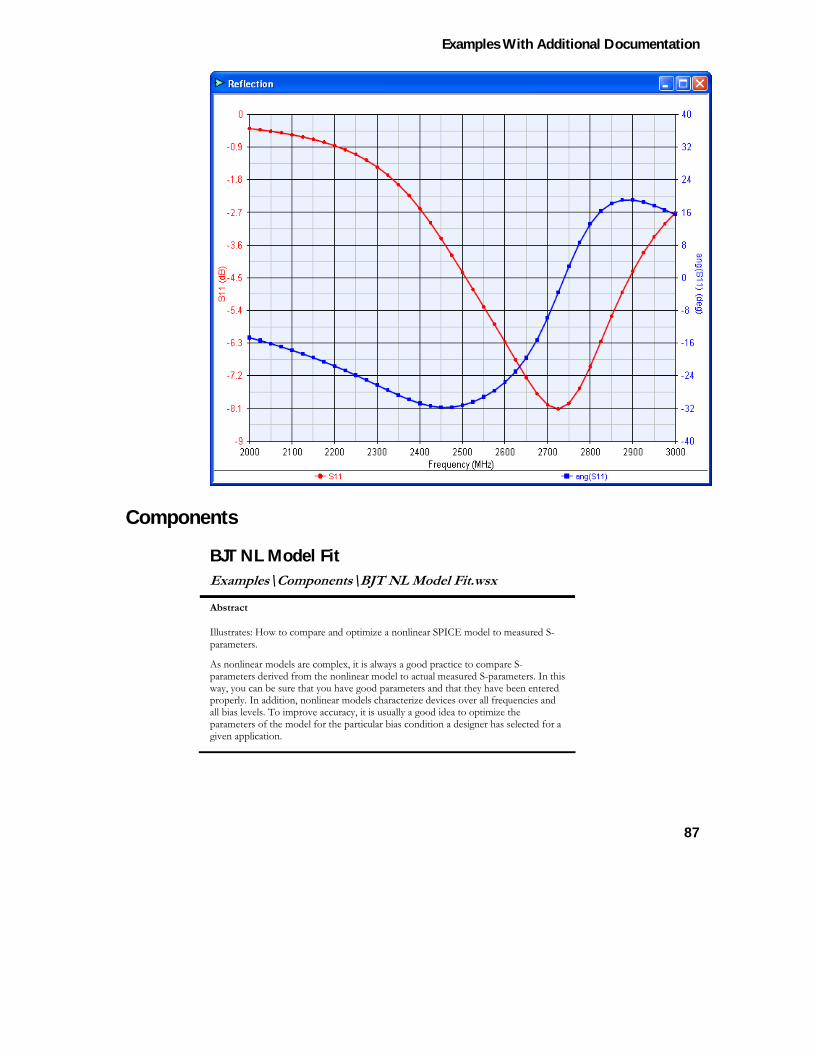
Examples With Additional Documentation
87
Components
BJT NL Model Fit Examples\Components\BJT NL Model Fit.wsx
Abstract
Illustrates: How to compare and optimize a nonlinear SPICE model to measured S-parameters.
As nonlinear models are complex, it is always a good practice to compare S-parameters derived from the nonlinear model to actual measured S-parameters. In this way, you can be sure that you have good parameters and that they have been entered properly. In addition, nonlinear models characterize devices over all frequencies and all bias levels. To improve accuracy, it is usually a good idea to optimize the parameters of the model for the particular bias condition a designer has selected for a given application.
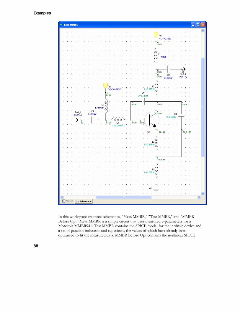
Examples
88
In this workspace are three schematics, "Meas MMBR," "Test MMBR," and "MMBR Before Opt" Meas MMBR is a simple circuit that uses measured S-parameters for a Motorola MMBR941. Test MMBR contains the SPICE model for the intrinsic device and a set of parasitic inductors and capacitors, the values of which have already been optimized to fit the measured data. MMBR Before Opt contains the nonlinear SPICE
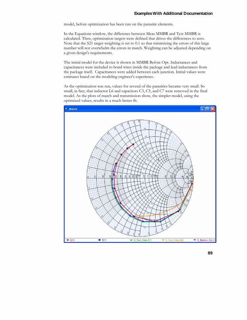
Examples With Additional Documentation
89
model, before optimization has been run on the parasitic elements. In the Equations window, the difference between Meas MMBR and Test MMBR is calculated. Then, optimization targets were defined that drives the differences to zero. Note that the S21 target weighting is set to 0.1 so that minimizing the errors of this large number will not overwhelm the errors in match. Weighting can be adjusted depending on a given design's requirements. The initial model for the device is shown in MMBR Before Opt. Inductances and capacitances were included to bond wires inside the package and lead inductances from the package itself. Capacitances were added between each junction. Initial values were estimates based on the modeling engineer's experience. As the optimization was run, values for several of the parasitics became very small. So small, in fact, that inductor L6 and capacitors C3, C5, and C7 were removed in the final model. As the plots of match and transmission show, the simpler model, using the optimized values, results in a much better fit.
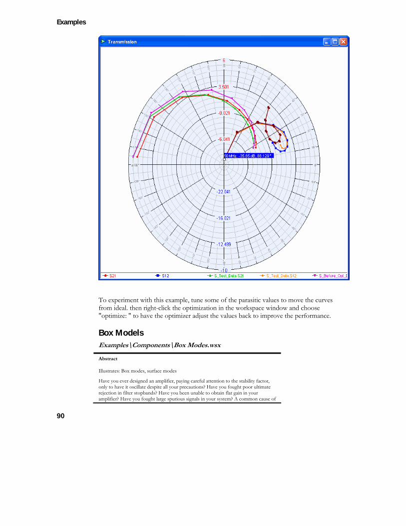
Examples
90
To experiment with this example, tune some of the parasitic values to move the curves from ideal. then right-click the optimization in the workspace window and choose "optimize: " to have the optimizer adjust the values back to improve the performance.
Box Models Examples\Components\Box Modes.wsx
Abstract
Illustrates: Box modes, surface modes
Have you ever designed an amplifier, paying careful attention to the stability factor, only to have it oscillate despite all your precautions? Have you fought poor ultimate rejection in filter stopbands? Have you been unable to obtain flat gain in your amplifier? Have you fought large spurious signals in your system? A common cause of
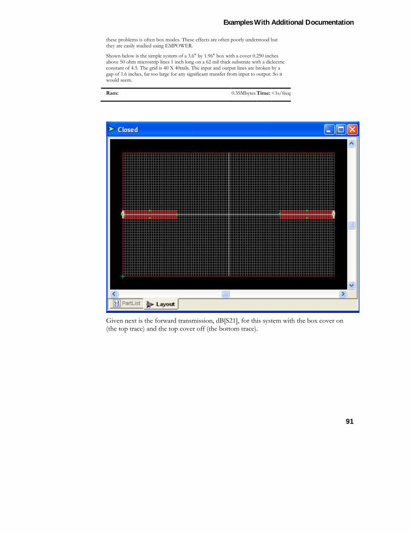
Examples With Additional Documentation
91
these problems is often box modes. These effects are often poorly understood but they are easily studied using EMPOWER.
Shown below is the simple system of a 3.6" by 1.96" box with a cover 0.250 inches above 50 ohm microstrip lines 1 inch long on a 62 mil thick substrate with a dielectric constant of 4.5. The grid is 40 X 40mils. The input and output lines are broken by a gap of 1.6 inches, far too large for any significant transfer from input to output. So it would seem.
Ram: 0.35Mbytes Time: <1s/freq
Given next is the forward transmission, dB[S21], for this system with the box cover on (the top trace) and the top cover off (the bottom trace).
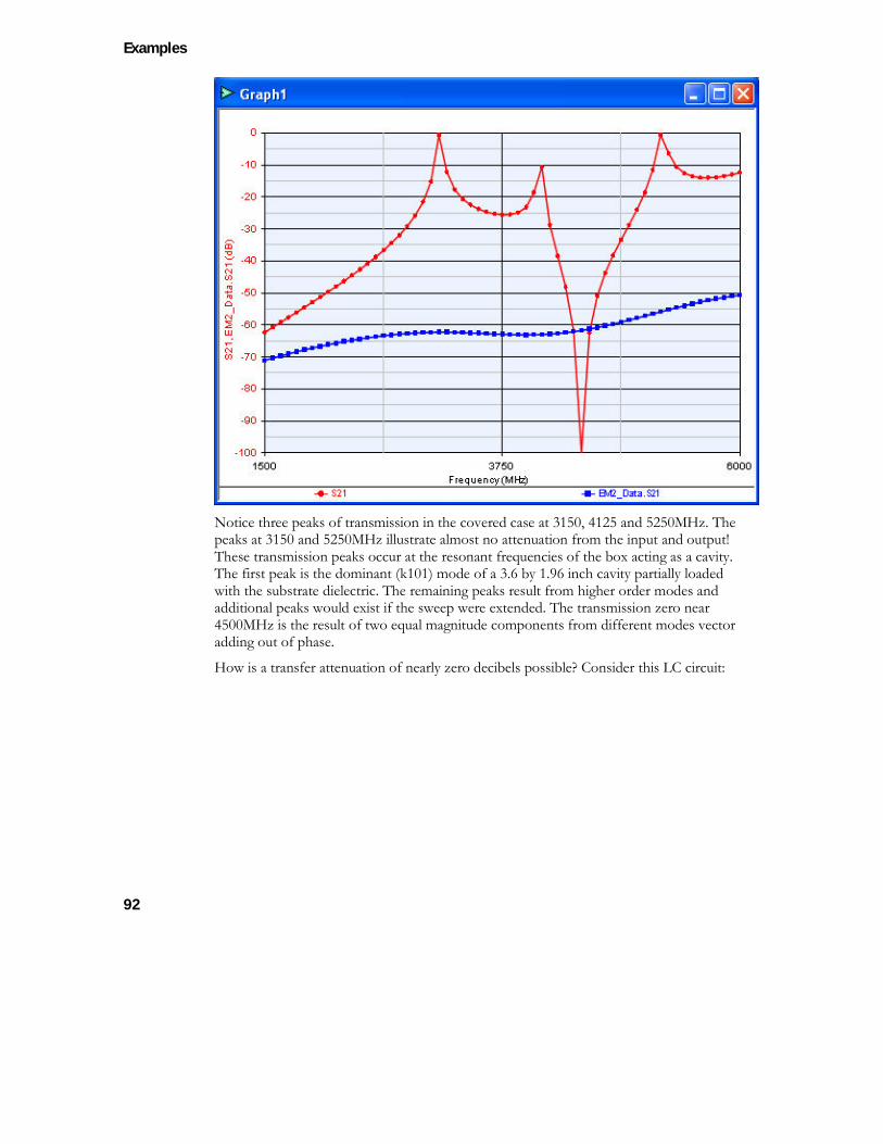
Examples
92
Notice three peaks of transmission in the covered case at 3150, 4125 and 5250MHz. The peaks at 3150 and 5250MHz illustrate almost no attenuation from the input and output! These transmission peaks occur at the resonant frequencies of the box acting as a cavity. The first peak is the dominant (k101) mode of a 3.6 by 1.96 inch cavity partially loaded with the substrate dielectric. The remaining peaks result from higher order modes and additional peaks would exist if the sweep were extended. The transmission zero near 4500MHz is the result of two equal magnitude components from different modes vector adding out of phase.
How is a transfer attenuation of nearly zero decibels possible? Consider this LC circuit:
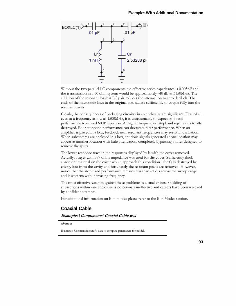
Examples With Additional Documentation
93
Without the two parallel LC components the effective series capacitance is 0.005pF and the transmission in a 50 ohm system would be approximately -40 dB at 3150MHz. The addition of the resonant lossless LC pair reduces the attenuation to zero decibels. The ends of the microstrip lines in the original box radiate sufficiently to couple fully into the resonant cavity.
Clearly, the consequences of packaging circuitry in an enclosure are significant. First of all, even at a frequency as low as 1500MHz, it is unreasonable to expect stopband performance to exceed 60dB rejection. At higher frequencies, stopband rejection is totally destroyed. Poor stopband performance can devastate filter performance. When an amplifier is placed in a box, feedback near resonant frequencies may result in oscillation. When subsystems are enclosed in a box, spurious signals generated at one location may appear at another location with little attenuation, completely bypassing a filter designed to remove the spurs.
The lower response trace in the responses displayed by is with the cover removed. Actually, a layer with 377 ohms impedance was used for the cover. Sufficiently thick absorbent material on the cover would approach this condition. The Q is destroyed by energy lost from the cavity and fortunately the resonant peaks are removed. However, notice that the stop band performance remains less than -60dB across the sweep range and it worsens with increasing frequency.
The most effective weapon against these problems is a smaller box. Shielding of subsections within one enclosure is notoriously ineffective and careers have been wrecked by confident attempts.
For additional information on Box modes please refer to the Box Modes section.
Coaxial Cable Examples\Components\Coaxial Cable.wsx
Abstract
Illustrates: Use manufacturer's data to compute parameters for model.
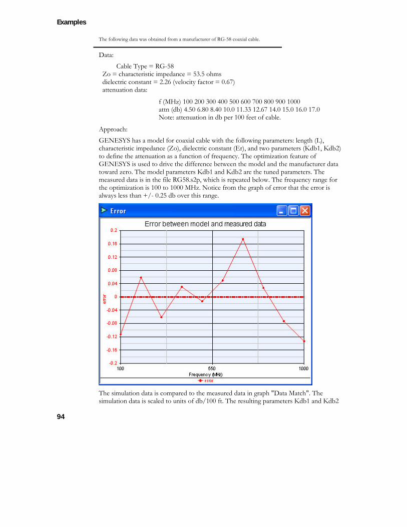
Examples
94
The following data was obtained from a manufacturer of RG-58 coaxial cable.
Data: Cable Type = RG-58 Zo = characteristic impedance = 53.5 ohms dielectric constant = 2.26 (velocity factor = 0.67) attenuation data:
f (MHz) 100 200 300 400 500 600 700 800 900 1000 attn (db) 4.50 6.80 8.40 10.0 11.33 12.67 14.0 15.0 16.0 17.0 Note: attenuation in db per 100 feet of cable.
Approach: GENESYS has a model for coaxial cable with the following parameters: length (L), characteristic impedance (Zo), dielectric constant (Er), and two parameters (Kdb1, Kdb2) to define the attenuation as a function of frequency. The optimization feature of GENESYS is used to drive the difference between the model and the manufacturer data toward zero. The model parameters Kdb1 and Kdb2 are the tuned parameters. The measured data is in the file RG58.s2p, which is repeated below. The frequency range for the optimization is 100 to 1000 MHz. Notice from the graph of error that the error is always less than +/- 0.25 db over this range.
The simulation data is compared to the measured data in graph "Data Match". The simulation data is scaled to units of db/100 ft. The resulting parameters Kdb1 and Kdb2
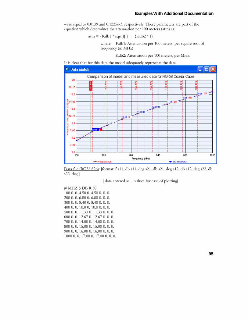
Examples With Additional Documentation
95
were equal to 0.0139 and 0.1225e-3, respectively. These parameters are part of the equation which determines the attenuation per 100 meters (attn) as:
attn = Kdb1 * sqrt[f] + Kdb2 * f
where: Kdb1: Attenuation per 100 meters, per square root of frequency (in MHz)
Kdb2: Attenuation per 100 meters, per MHz.
It is clear that for this data the model adequately represents the data.
Data file (RG58.S2p): [format: f s11_db s11_deg s21_db s21_deg s12_db s12_deg s22_db s22_deg ]
[ data entered as + values for ease of plotting]
# MHZ S DB R 50 100 0. 0. 4.50 0. 4.50 0. 0. 0. 200 0. 0. 6.80 0. 6.80 0. 0. 0. 300 0. 0. 8.40 0. 8.40 0. 0. 0. 400 0. 0. 10.0 0. 10.0 0. 0. 0. 500 0. 0. 11.33 0. 11.33 0. 0. 0. 600 0. 0. 12.67 0. 12.67 0. 0. 0. 700 0. 0. 14.00 0. 14.00 0. 0. 0. 800 0. 0. 15.00 0. 15.00 0. 0. 0. 900 0. 0. 16.00 0. 16.00 0. 0. 0. 1000 0. 0. 17.00 0. 17.00 0. 0. 0.
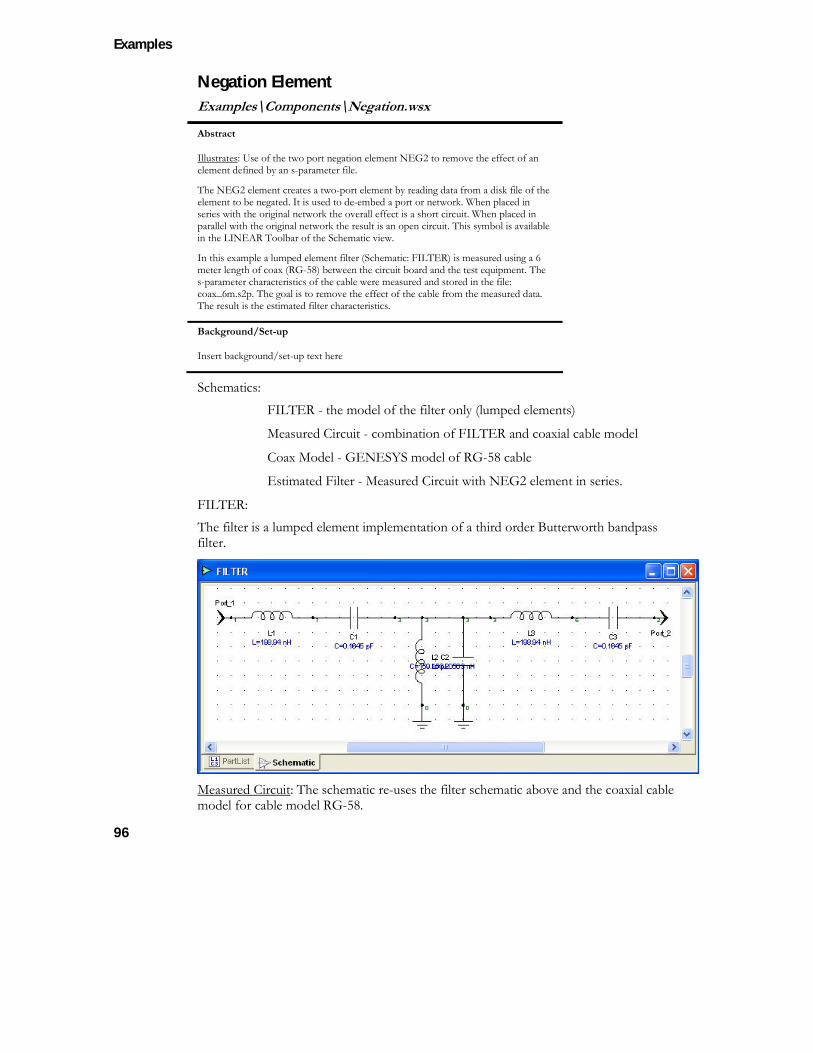
Examples
96
Negation Element Examples\Components\Negation.wsx
Abstract
Illustrates: Use of the two port negation element NEG2 to remove the effect of an element defined by an s-parameter file.
The NEG2 element creates a two-port element by reading data from a disk file of the element to be negated. It is used to de-embed a port or network. When placed in series with the original network the overall effect is a short circuit. When placed in parallel with the original network the result is an open circuit. This symbol is available in the LINEAR Toolbar of the Schematic view.
In this example a lumped element filter (Schematic: FILTER) is measured using a 6 meter length of coax (RG-58) between the circuit board and the test equipment. The s-parameter characteristics of the cable were measured and stored in the file: coax_6m.s2p. The goal is to remove the effect of the cable from the measured data. The result is the estimated filter characteristics.
Background/Set-up
Insert background/set-up text here
Schematics: FILTER - the model of the filter only (lumped elements)
Measured Circuit - combination of FILTER and coaxial cable model
Coax Model - GENESYS model of RG-58 cable
Estimated Filter - Measured Circuit with NEG2 element in series.
FILTER: The filter is a lumped element implementation of a third order Butterworth bandpass filter.
Measured Circuit: The schematic re-uses the filter schematic above and the coaxial cable model for cable model RG-58.
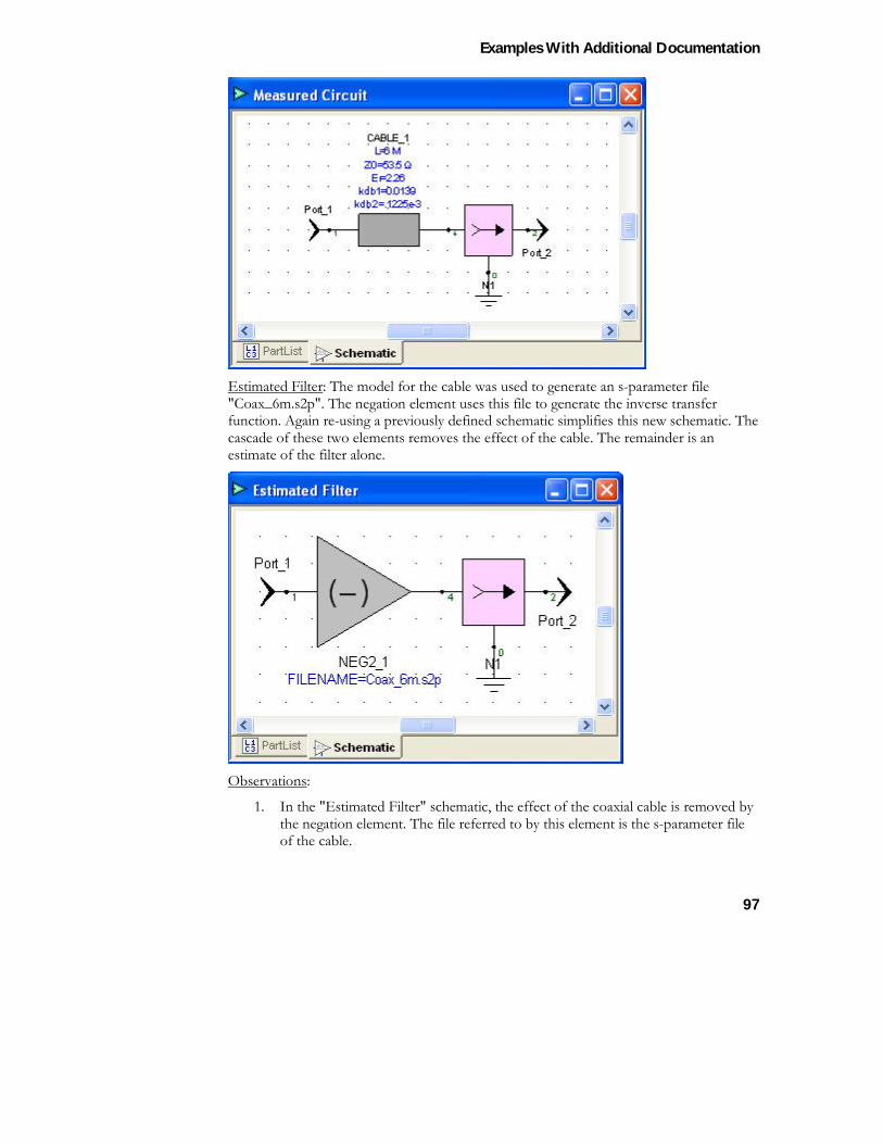
Examples With Additional Documentation
97
Estimated Filter: The model for the cable was used to generate an s-parameter file "Coax_6m.s2p". The negation element uses this file to generate the inverse transfer function. Again re-using a previously defined schematic simplifies this new schematic. The cascade of these two elements removes the effect of the cable. The remainder is an estimate of the filter alone.
Observations:
1. In the "Estimated Filter" schematic, the effect of the coaxial cable is removed by the negation element. The file referred to by this element is the s-parameter file of the cable.
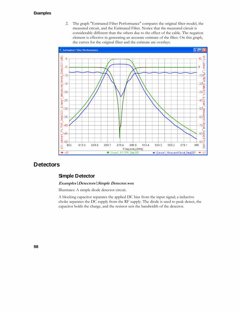
Examples
98
2. The graph "Estimated Filter Performance" compares the original filter model, the measured circuit, and the Estimated Filter. Notice that the measured circuit is considerably different than the others due to the effect of the cable. The negation element is effective in generating an accurate estimate of the filter. On this graph, the curves for the original filter and the estimate are overlays.
Detectors
Simple Detector Examples\Detectors\Simple Detector.wsx Illustrates: A simple diode detector circuit.
A blocking capacitor separates the applied DC bias from the input signal; a inductive choke separates the DC supply from the RF supply. The diode is used to peak detect, the capacitor holds the charge, and the resistor sets the bandwidth of the detector.
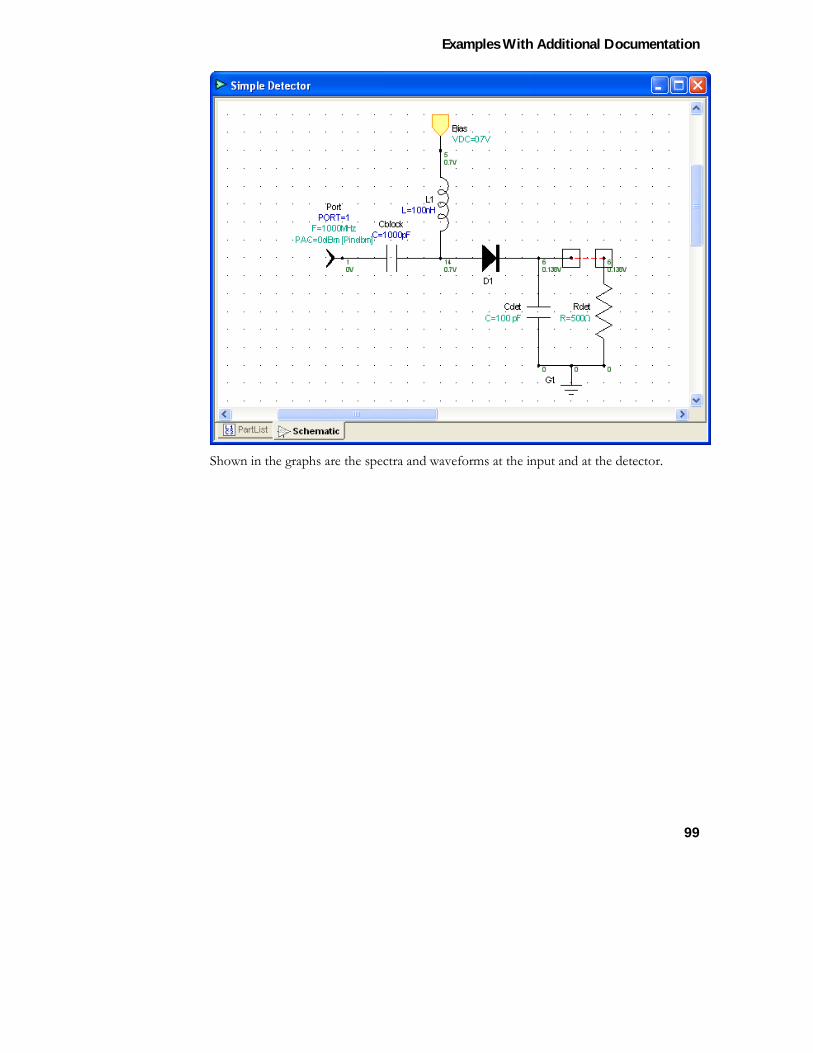
Examples With Additional Documentation
99
Shown in the graphs are the spectra and waveforms at the input and at the detector.
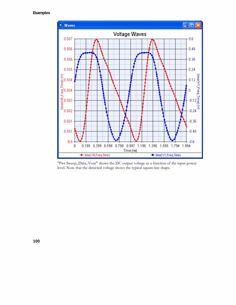
Examples
100
"Pwr Sweep_Data_Vout" shows the DC output voltage as a function of the input power level. Note that the detected voltage shows the typical square-law shape.
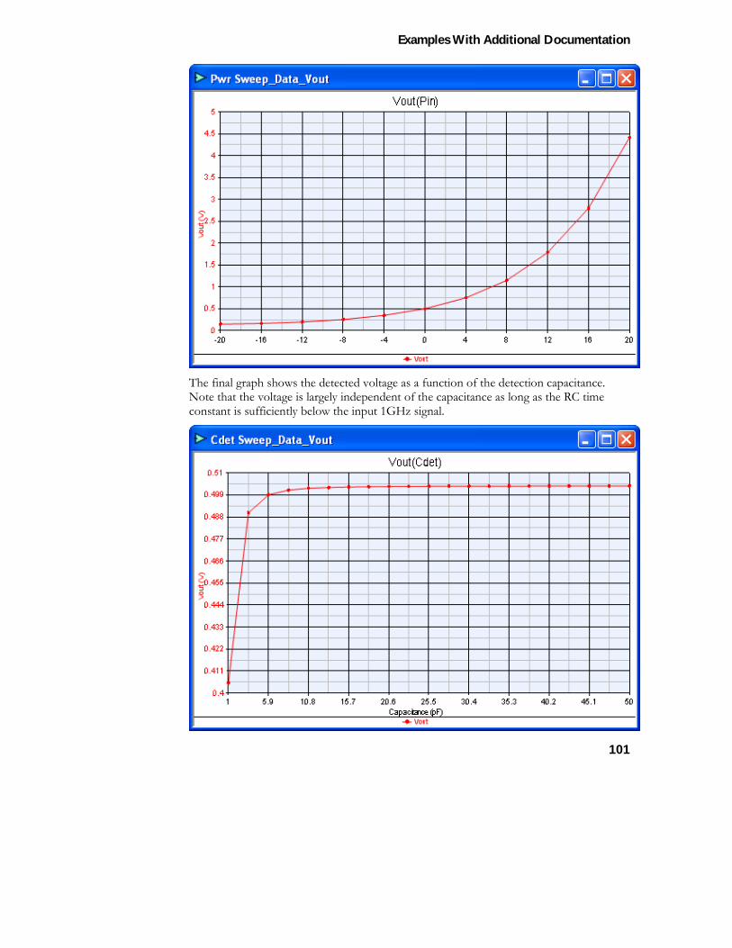
Examples With Additional Documentation
101
The final graph shows the detected voltage as a function of the detection capacitance. Note that the voltage is largely independent of the capacitance as long as the RC time constant is sufficiently below the input 1GHz signal.
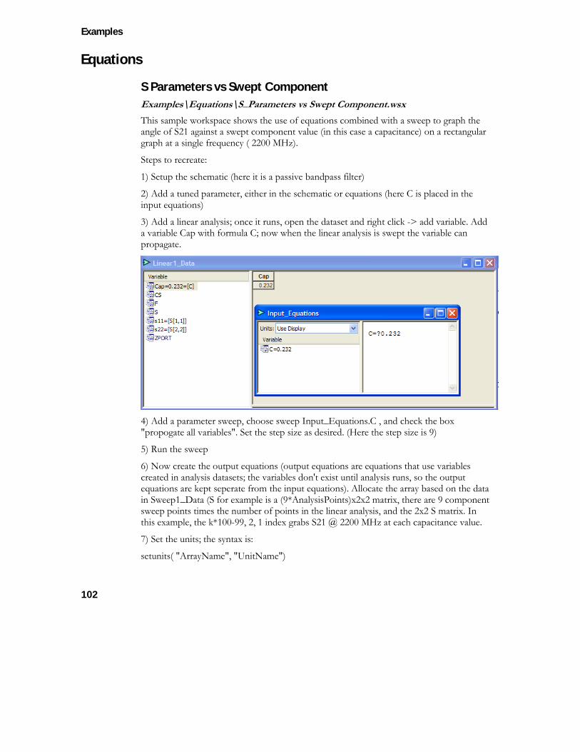
Examples
102
Equations
S Parameters vs Swept Component Examples\Equations\S_Parameters vs Swept Component.wsx This sample workspace shows the use of equations combined with a sweep to graph the angle of S21 against a swept component value (in this case a capacitance) on a rectangular graph at a single frequency ( 2200 MHz).
Steps to recreate:
1) Setup the schematic (here it is a passive bandpass filter)
2) Add a tuned parameter, either in the schematic or equations (here C is placed in the input equations)
3) Add a linear analysis; once it runs, open the dataset and right click -> add variable. Add a variable Cap with formula C; now when the linear analysis is swept the variable can propagate.
4) Add a parameter sweep, choose sweep Input_Equations.C , and check the box "propogate all variables". Set the step size as desired. (Here the step size is 9)
5) Run the sweep
6) Now create the output equations (output equations are equations that use variables created in analysis datasets; the variables don't exist until analysis runs, so the output equations are kept seperate from the input equations). Allocate the array based on the data in Sweep1_Data (S for example is a (9*AnalysisPoints)x2x2 matrix, there are 9 component sweep points times the number of points in the linear analysis, and the 2x2 S matrix. In this example, the k*100-99, 2, 1 index grabs S21 @ 2200 MHz at each capacitance value.
7) Set the units; the syntax is:
setunits( "ArrayName", "UnitName")
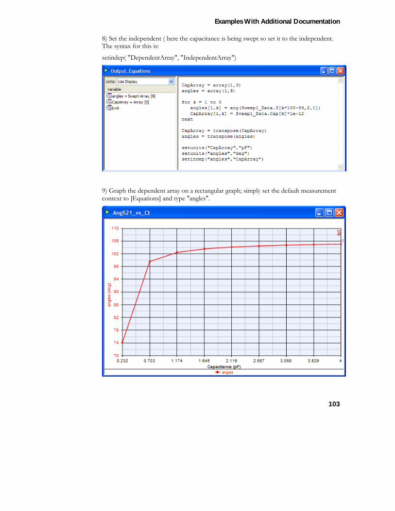
Examples With Additional Documentation
103
8) Set the independent ( here the capacitance is being swept so set it to the independent. The syntax for this is:
setindep( "DependentArray", "IndependentArray")
9) Graph the dependent array on a rectangular graph; simply set the default measurement context to [Equations] and type "angles".
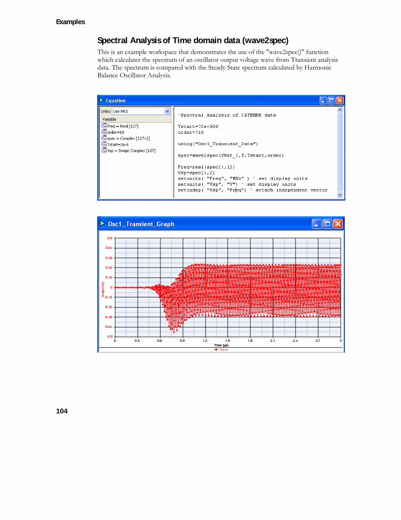
Examples
104
Spectral Analysis of Time domain data (wave2spec) This is an example workspace that demonstrates the use of the "wave2spec()" function which calculates the spectrum of an oscillator output voltage wave from Transient analysis data. The spectrum is compared with the Steady State spectrum calculated by Harmonic Balance Oscillator Analysis.
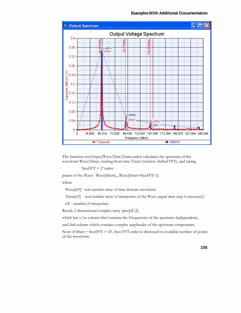
Examples With Additional Documentation
105
The function wave2spec(Wave,Time,Tstart,order) calculates the spectrum of the waveform Wave(Time), starting from time Tstart (window shifted FFT), and taking
SizeFFT = 2^order
points of the Wave: Wave[iStart],..,Wave[iStart+SizeFFT-1]
where
Wave[nT] - real number array of time domain waveform
Time[nT] - real number array of timepoints of the Wave (equal time step is necessary!)
nT - number of timepoints
Result: 2-dimensional complex array spec[nF,2],
which has a 1st column that contains the Frequencies of the spectrum (independent),
and 2nd column which contains complex amplitudes of the spectrum components.
Note: if iStart + SizeFFT > nT, then FFT order is decreased to available number of points of the waveform.

Examples
106
Note: The function suggests that timepoints of the waveform have fixed time step. Set checkbox "Force Output at Exact Step" of Transient solver/Output tab to ensure a fixed time step of transient analysis output waveform data.
To calculate Steady-State spectrum, set spectral analysis initial time point Tstart, where the waveform graph shows steady state solution. The initial phases of the calculated spectrum will be defined by the initial time of the spectrum calculation Tstart.
Example use of the wave2spec function:
Tstart=?2e-006
order=?10
using("Osc1_Transient_Data")
spec=wave2spec(VNet_1,T,Tstart,order)
Freq=real(spec[:,1]) ' extract frequencies of the spectrum where "[:,1]" means to use all indices in column 1
Vsp=spec[:,2] ' extract complex amplitudes of the spectrum
setunits( "Freq", "MHz" ) ' set frequency display units
setunits( "Vsp", "V") ' set spectrum amplitudes display units
setindep( "Vsp", "Freq") ' attach independent vector
Filters
Contiguous Diplexer Examples\Filters\Contiguous Diplexer.wsx This example illustrates the design of a contiguous diplex filter. It was designed by the following steps:
1. Design a 7th order singly-terminated Butterworth highpass filter using the synthesis program FILTER and write a file named CONTIGUS.SCH.
2. Return to FILTER. Design a 7th order singly-terminated Butterworth lowpass and write a file named LP.SCH. Then run GENESYS and display the lowpass response.
3. Open the schematic and draw a box around the entire lowpass schematic. Selecting “Cut” and “Paste” from the Edit menu places the lowpass schematic in the buffer and back in the schematic.
4. Next, load CONTIGUS.SCH, open the schematic, and select Paste from the Edit menu which drops the lowpass over the highpass. Drag the lowpass schematic off of the highpass schematic using the mouse.
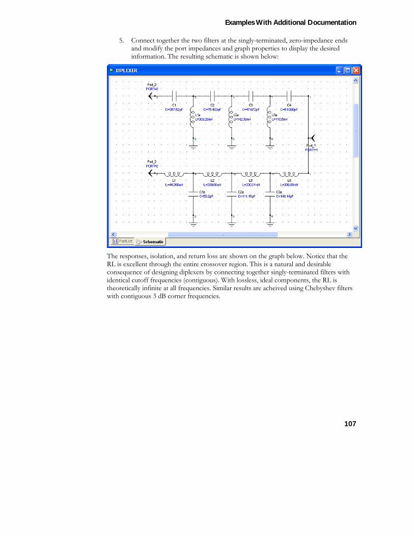
Examples With Additional Documentation
107
5. Connect together the two filters at the singly-terminated, zero-impedance ends and modify the port impedances and graph properties to display the desired information. The resulting schematic is shown below:
The responses, isolation, and return loss are shown on the graph below. Notice that the RL is excellent through the entire crossover region. This is a natural and desirable consequence of designing diplexers by connecting together singly-terminated filters with identical cutoff frequencies (contiguous). With lossless, ideal components, the RL is theoretically infinite at all frequencies. Similar results are acheived using Chebyshev filters with contiguous 3 dB corner frequencies.
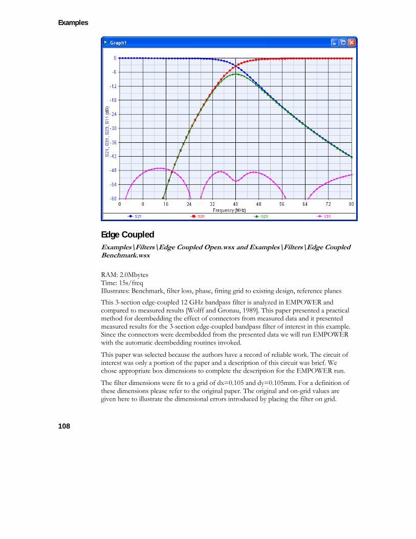
Examples
108
Edge Coupled Examples\Filters\Edge Coupled Open.wsx and Examples\Filters\Edge Coupled Benchmark.wsx RAM: 2.0Mbytes Time: 15s/freq Illustrates: Benchmark, filter loss, phase, fitting grid to existing design, reference planes This 3-section edge-coupled 12 GHz bandpass filter is analyzed in EMPOWER and compared to measured results [Wolff and Gronau, 1989]. This paper presented a practical method for deembedding the effect of connectors from measured data and it presented measured results for the 3-section edge-coupled bandpass filter of interest in this example. Since the connectors were deembedded from the presented data we will run EMPOWER with the automatic deembedding routines invoked.
This paper was selected because the authors have a record of reliable work. The circuit of interest was only a portion of the paper and a description of this circuit was brief. We chose appropriate box dimensions to complete the description for the EMPOWER run.
The filter dimensions were fit to a grid of dx=0.105 and dy=0.105mm. For a definition of these dimensions please refer to the original paper. The original and on-grid values are given here to illustrate the dimensional errors introduced by placing the filter on grid.
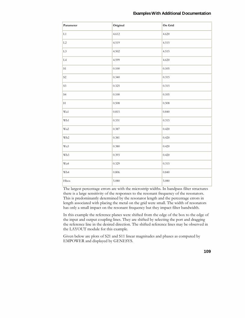
Examples With Additional Documentation
109
Parameter Original On Grid
L1 4.612 4.620
L2 4.519 4.515
L3 4.502 4.515
L4 4.599 4.620
S1 0.100 0.105
S2 0.340 0.315
S3 0.325 0.315
S4 0.100 0.105
H 0.508 0.508
Wa1 0.815 0.840
Wb1 0.331 0.315
Wa2 0.387 0.420
Wb2 0.381 0.420
Wa3 0.380 0.420
Wb3 0.393 0.420
Wa4 0.329 0.315
Wb4 0.806 0.840
Hbox 5.080 5.080
The largest percentage errors are with the microstrip widths. In bandpass filter structures there is a large sensitivity of the responses to the resonant frequency of the resonators. This is predominantly determined by the resonator length and the percentage errors in length associated with placing the metal on the grid were small. The width of resonators has only a small impact on the resonant frequency but they impact filter bandwidth.
In this example the reference planes were shifted from the edge of the box to the edge of the input and output coupling lines. They are shifted by selecting the port and dragging the reference line in the desired direction. The shifted reference lines may be observed in the LAYOUT module for this example.
Given below are plots of S21 and S11 linear magnitudes and phases as computed by EMPOWER and displayed by GENESYS.
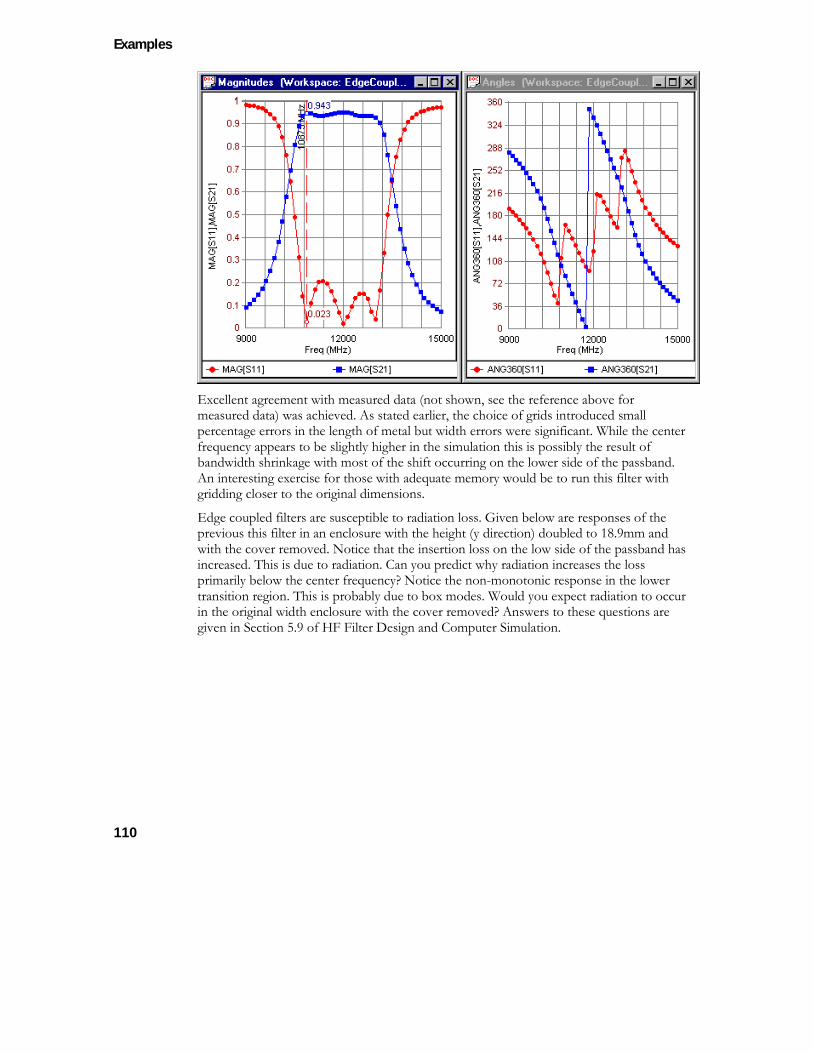
Examples
110
Excellent agreement with measured data (not shown, see the reference above for measured data) was achieved. As stated earlier, the choice of grids introduced small percentage errors in the length of metal but width errors were significant. While the center frequency appears to be slightly higher in the simulation this is possibly the result of bandwidth shrinkage with most of the shift occurring on the lower side of the passband. An interesting exercise for those with adequate memory would be to run this filter with gridding closer to the original dimensions.
Edge coupled filters are susceptible to radiation loss. Given below are responses of the previous this filter in an enclosure with the height (y direction) doubled to 18.9mm and with the cover removed. Notice that the insertion loss on the low side of the passband has increased. This is due to radiation. Can you predict why radiation increases the loss primarily below the center frequency? Notice the non-monotonic response in the lower transition region. This is probably due to box modes. Would you expect radiation to occur in the original width enclosure with the cover removed? Answers to these questions are given in Section 5.9 of HF Filter Design and Computer Simulation.
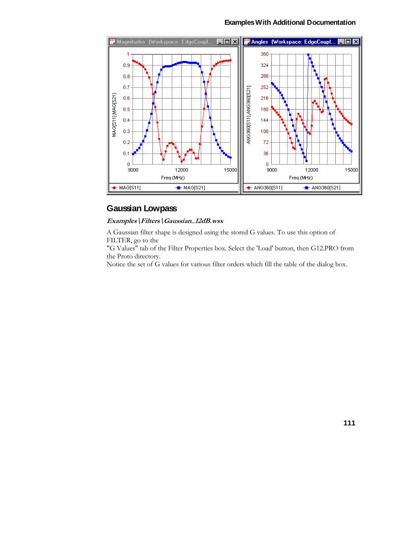
Examples With Additional Documentation
111
Gaussian Lowpass Examples\Filters\Gaussian_12dB.wsx A Gaussian filter shape is designed using the stored G values. To use this option of FILTER, go to the "G Values" tab of the Filter Properties box. Select the 'Load' button, then G12.PRO from the Proto directory. Notice the set of G values for various filter orders which fill the table of the dialog box.
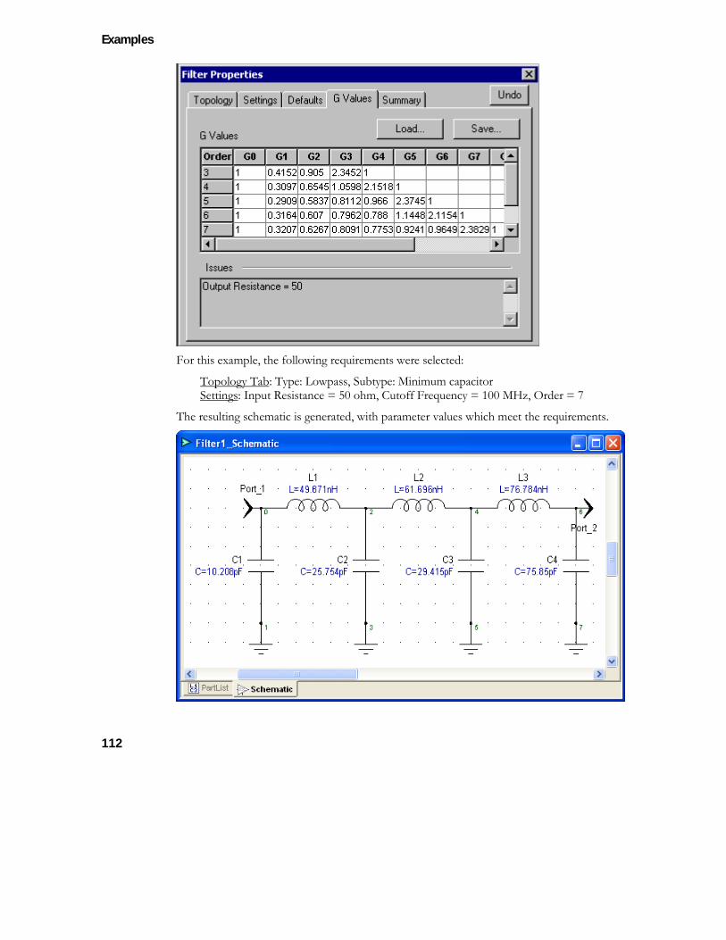
Examples
112
For this example, the following requirements were selected:
Topology Tab: Type: Lowpass, Subtype: Minimum capacitor Settings: Input Resistance = 50 ohm, Cutoff Frequency = 100 MHz, Order = 7
The resulting schematic is generated, with parameter values which meet the requirements.
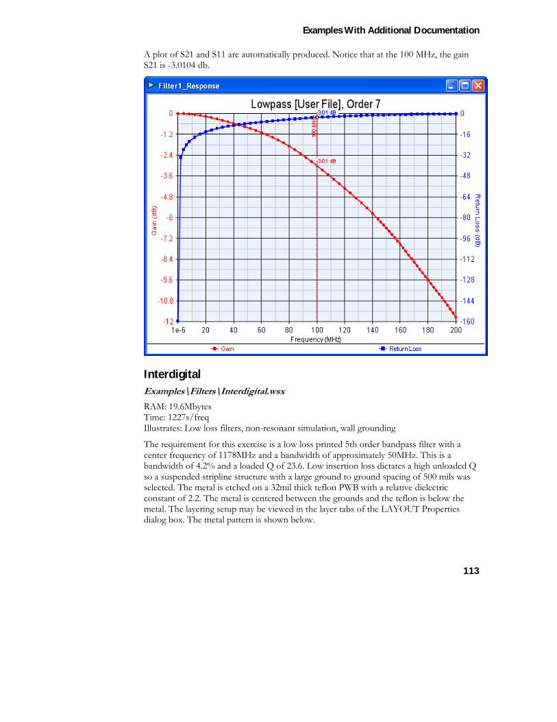
Examples With Additional Documentation
113
A plot of S21 and S11 are automatically produced. Notice that at the 100 MHz, the gain S21 is -3.0104 db.
Interdigital Examples\Filters\Interdigital.wsx RAM: 19.6Mbytes Time: 1227s/freq Illustrates: Low loss filters, non-resonant simulation, wall grounding
The requirement for this exercise is a low loss printed 5th order bandpass filter with a center frequency of 1178MHz and a bandwidth of approximately 50MHz. This is a bandwidth of 4.2% and a loaded Q of 23.6. Low insertion loss dictates a high unloaded Q so a suspended stripline structure with a large ground to ground spacing of 500 mils was selected. The metal is etched on a 32mil thick teflon PWB with a relative dielectric constant of 2.2. The metal is centered between the grounds and the teflon is below the metal. The layering setup may be viewed in the layer tabs of the LAYOUT Properties dialog box. The metal pattern is shown below.
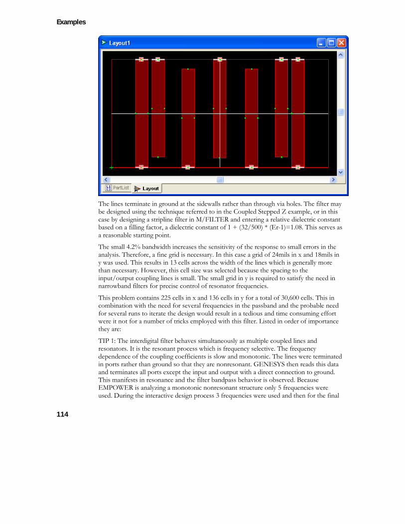
Examples
114
The lines terminate in ground at the sidewalls rather than through via holes. The filter may be designed using the technique referred to in the Coupled Stepped Z example, or in this case by designing a stripline filter in M/FILTER and entering a relative dielectric constant based on a filling factor, a dielectric constant of 1 + (32/500) * (Er-1)=1.08. This serves as a reasonable starting point.
The small 4.2% bandwidth increases the sensitivity of the response to small errors in the analysis. Therefore, a fine grid is necessary. In this case a grid of 24mils in x and 18mils in y was used. This results in 13 cells across the width of the lines which is generally more than necessary. However, this cell size was selected because the spacing to the input/output coupling lines is small. The small grid in y is required to satisfy the need in narrowband filters for precise control of resonator frequencies.
This problem contains 225 cells in x and 136 cells in y for a total of 30,600 cells. This in combination with the need for several frequencies in the passband and the probable need for several runs to iterate the design would result in a tedious and time consuming effort were it not for a number of tricks employed with this filter. Listed in order of importance they are:
TIP 1: The interdigital filter behaves simultaneously as multiple coupled lines and resonators. It is the resonant process which is frequency selective. The frequency dependence of the coupling coefficients is slow and monotonic. The lines were terminated in ports rather than ground so that they are nonresonant. GENESYS then reads this data and terminates all ports except the input and output with a direct connection to ground. This manifests in resonance and the filter bandpass behavior is observed. Because EMPOWER is analyzing a monotonic nonresonant structure only 5 frequencies were used. During the interactive design process 3 frequencies were used and then for the final
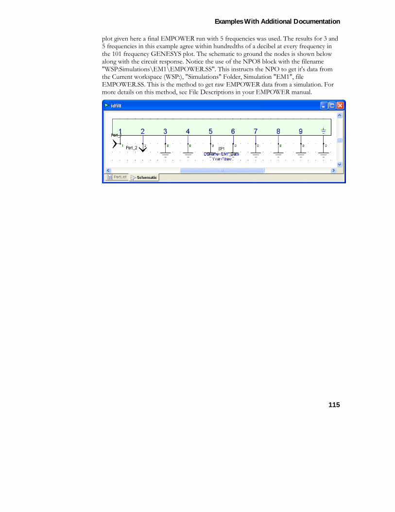
Examples With Additional Documentation
115
plot given here a final EMPOWER run with 5 frequencies was used. The results for 3 and 5 frequencies in this example agree within hundredths of a decibel at every frequency in the 101 frequency GENESYS plot. The schematic to ground the nodes is shown below along with the circuit response. Notice the use of the NPO8 block with the filename "WSP:Simulations\EM1\EMPOWER.SS". This instructs the NPO to get it's data from the Current workspace (WSP:), "Simulations" Folder, Simulation "EM1", file EMPOWER.SS. This is the method to get raw EMPOWER data from a simulation. For more details on this method, see File Descriptions in your EMPOWER manual.
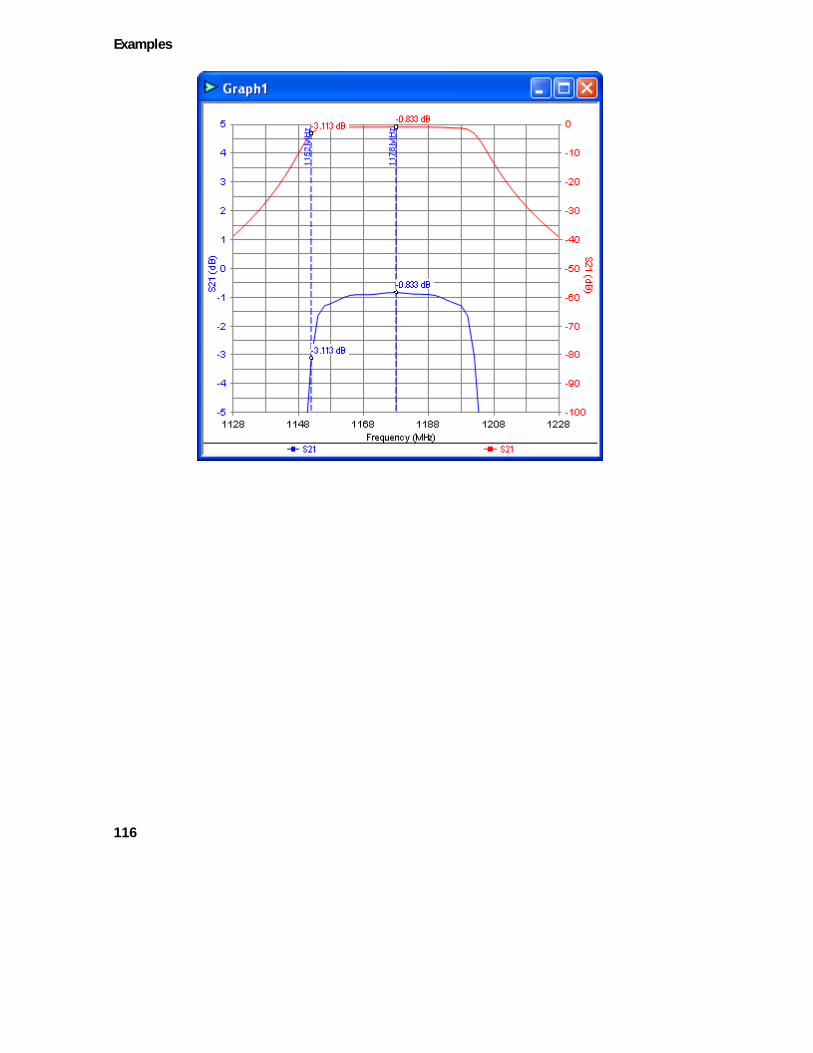
Examples
116
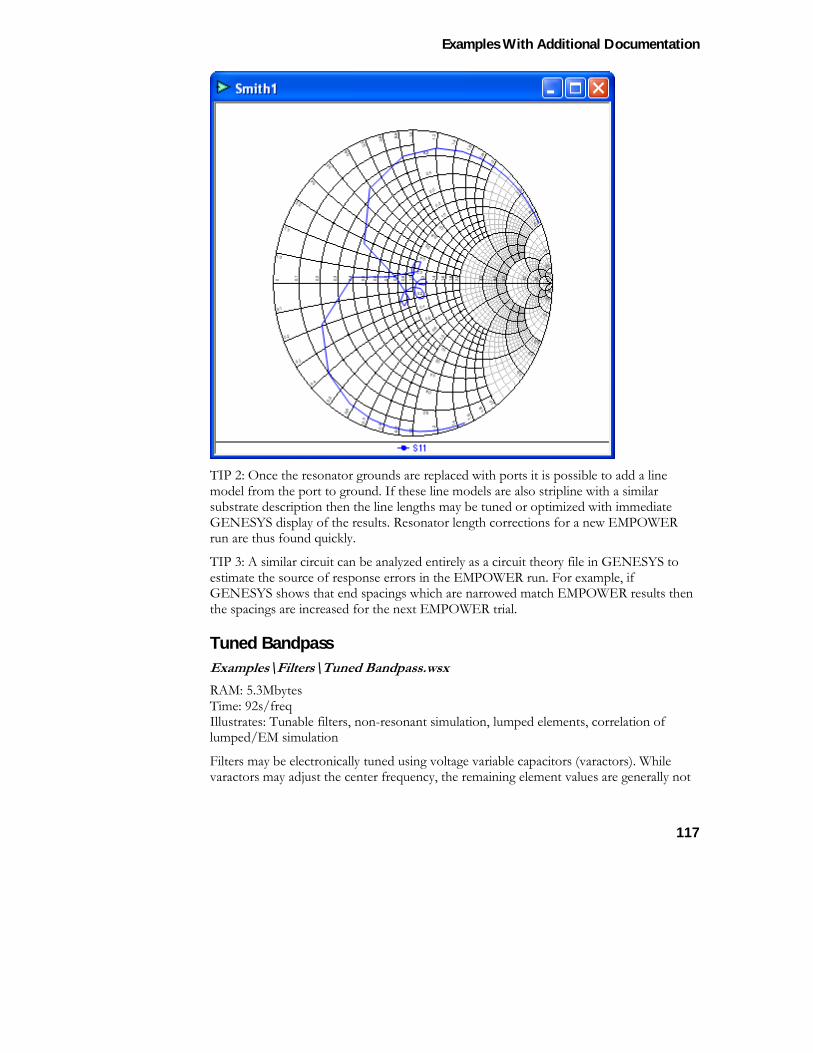
Examples With Additional Documentation
117
TIP 2: Once the resonator grounds are replaced with ports it is possible to add a line model from the port to ground. If these line models are also stripline with a similar substrate description then the line lengths may be tuned or optimized with immediate GENESYS display of the results. Resonator length corrections for a new EMPOWER run are thus found quickly.
TIP 3: A similar circuit can be analyzed entirely as a circuit theory file in GENESYS to estimate the source of response errors in the EMPOWER run. For example, if GENESYS shows that end spacings which are narrowed match EMPOWER results then the spacings are increased for the next EMPOWER trial.
Tuned Bandpass Examples\Filters\Tuned Bandpass.wsx RAM: 5.3Mbytes Time: 92s/freq Illustrates: Tunable filters, non-resonant simulation, lumped elements, correlation of lumped/EM simulation
Filters may be electronically tuned using voltage variable capacitors (varactors). While varactors may adjust the center frequency, the remaining element values are generally not
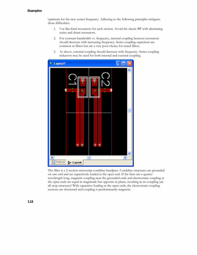
Examples
118
optimum for the new center frequency. Adhering to the following principles mitigates these difficulties:
1. Use like-kind resonators for each section. Avoid the classic BP with alternating series and shunt resonators.
2. For constant bandwidth vs. frequency, internal coupling between resonators should decrease with increasing frequency. Series coupling capacitors are common in filters but are a very poor choice for tuned filters.
3. As above, external coupling should decrease with frequency. Series coupling inductors may be used for both internal and external coupling.
The filter is a 2-section microstrip combline bandpass. Combline structures are grounded on one end and are capacitively loaded at the open end. If the lines are a quarter wavelength long, magnetic coupling near the grounded ends and electrostatic coupling at the open ends are equal in magnitude but opposite in phase, resulting in no coupling (an all-stop structure)! With capacitive loading at the open ends, the electrostatic coupling sections are shortened and coupling is predominantly magnetic.
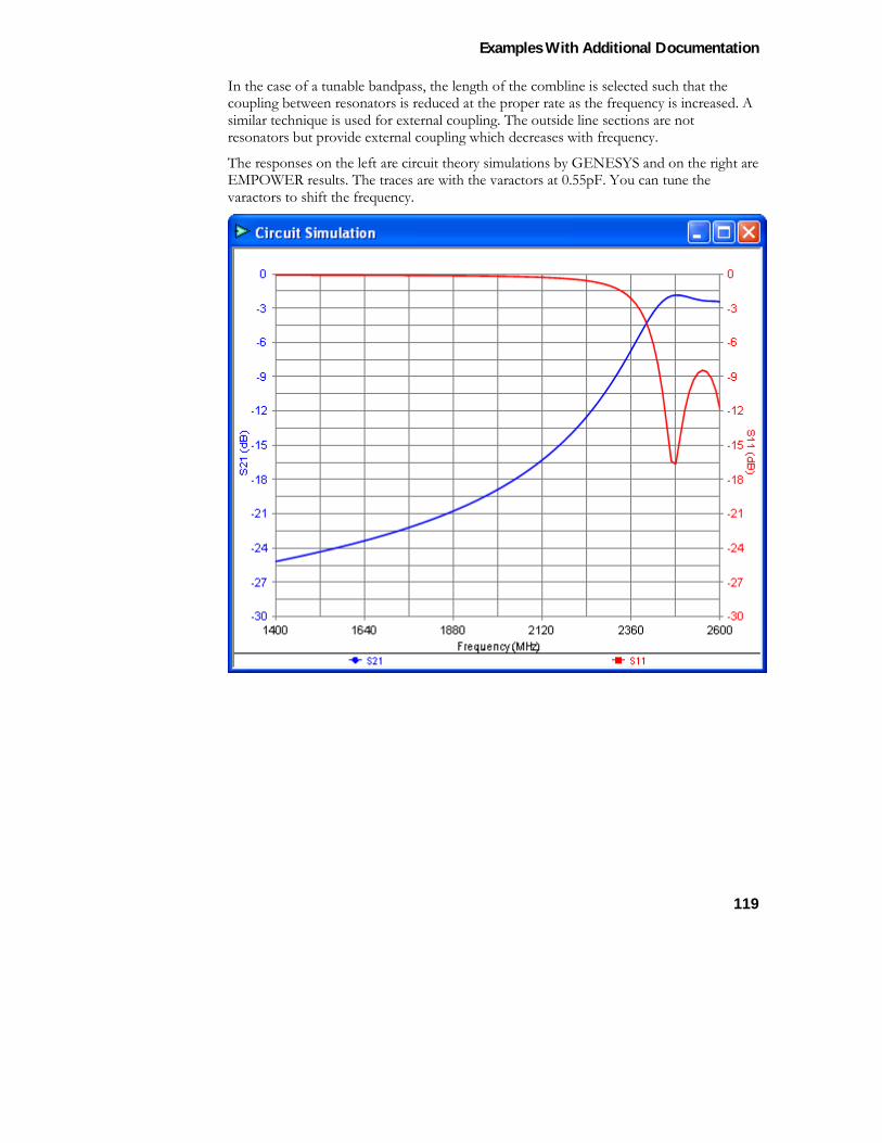
Examples With Additional Documentation
119
In the case of a tunable bandpass, the length of the combline is selected such that the coupling between resonators is reduced at the proper rate as the frequency is increased. A similar technique is used for external coupling. The outside line sections are not resonators but provide external coupling which decreases with frequency.
The responses on the left are circuit theory simulations by GENESYS and on the right are EMPOWER results. The traces are with the varactors at 0.55pF. You can tune the varactors to shift the frequency.
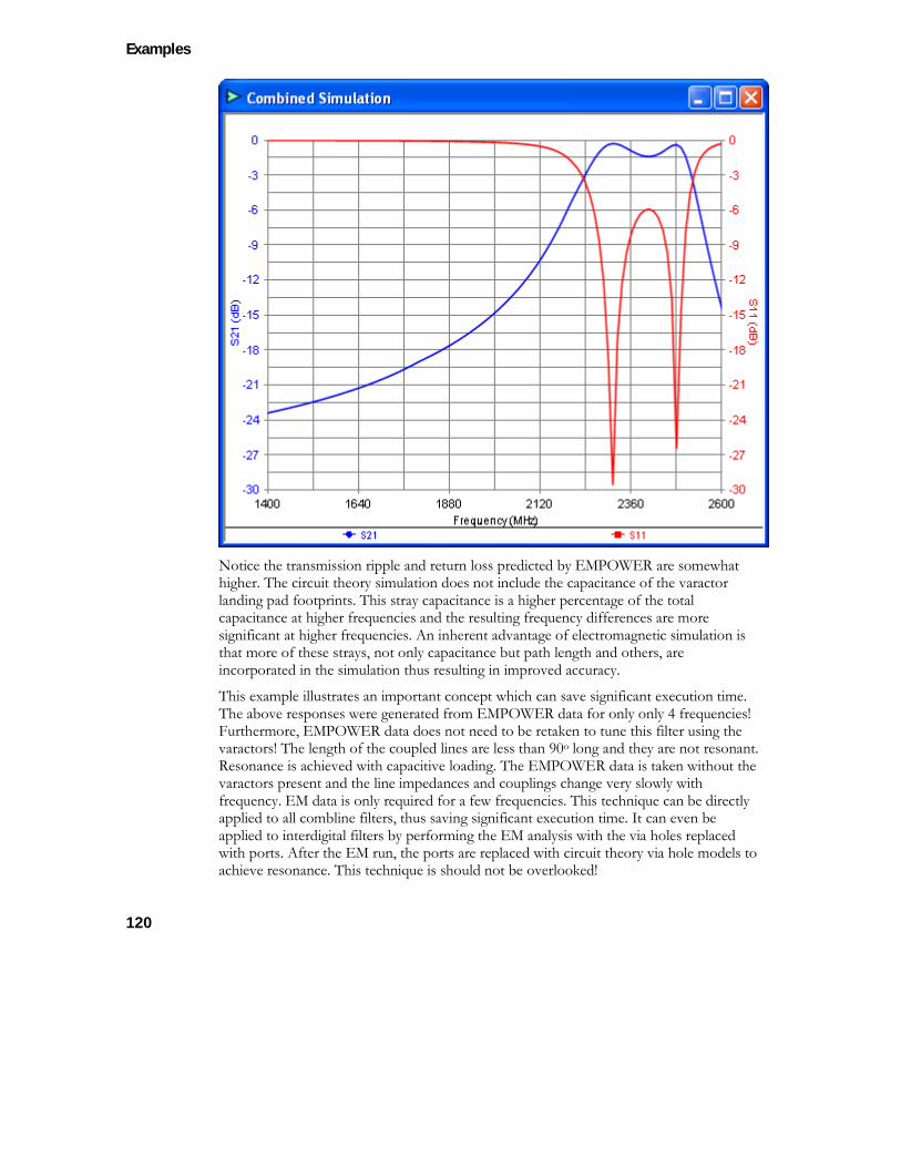
Examples
120
Notice the transmission ripple and return loss predicted by EMPOWER are somewhat higher. The circuit theory simulation does not include the capacitance of the varactor landing pad footprints. This stray capacitance is a higher percentage of the total capacitance at higher frequencies and the resulting frequency differences are more significant at higher frequencies. An inherent advantage of electromagnetic simulation is that more of these strays, not only capacitance but path length and others, are incorporated in the simulation thus resulting in improved accuracy.
This example illustrates an important concept which can save significant execution time. The above responses were generated from EMPOWER data for only only 4 frequencies! Furthermore, EMPOWER data does not need to be retaken to tune this filter using the varactors! The length of the coupled lines are less than 90o long and they are not resonant. Resonance is achieved with capacitive loading. The EMPOWER data is taken without the varactors present and the line impedances and couplings change very slowly with frequency. EM data is only required for a few frequencies. This technique can be directly applied to all combline filters, thus saving significant execution time. It can even be applied to interdigital filters by performing the EM analysis with the via holes replaced with ports. After the EM run, the ports are replaced with circuit theory via hole models to achieve resonance. This technique is should not be overlooked!
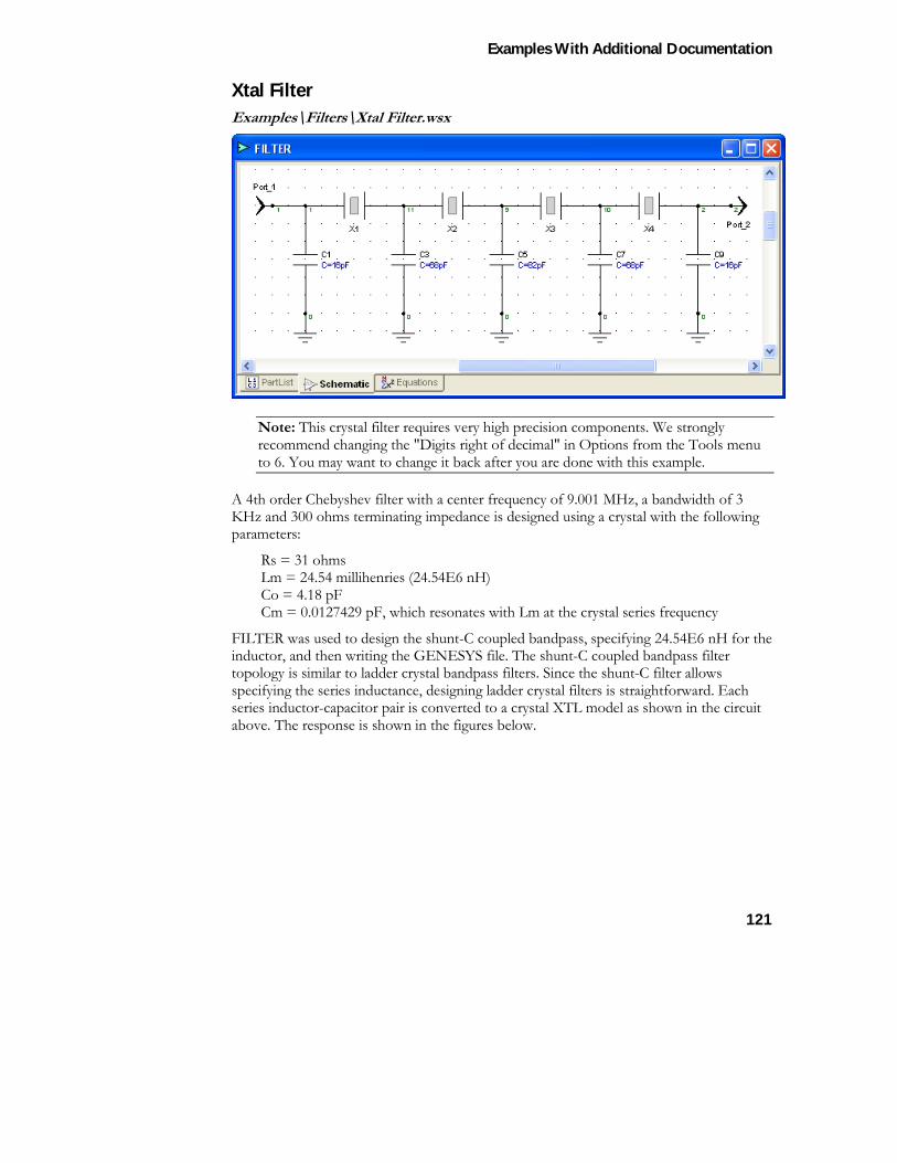
Examples With Additional Documentation
121
Xtal Filter Examples\Filters\Xtal Filter.wsx
Note: This crystal filter requires very high precision components. We strongly recommend changing the "Digits right of decimal" in Options from the Tools menu to 6. You may want to change it back after you are done with this example.
A 4th order Chebyshev filter with a center frequency of 9.001 MHz, a bandwidth of 3 KHz and 300 ohms terminating impedance is designed using a crystal with the following parameters:
Rs = 31 ohms Lm = 24.54 millihenries (24.54E6 nH) Co = 4.18 pF Cm = 0.0127429 pF, which resonates with Lm at the crystal series frequency
FILTER was used to design the shunt-C coupled bandpass, specifying 24.54E6 nH for the inductor, and then writing the GENESYS file. The shunt-C coupled bandpass filter topology is similar to ladder crystal bandpass filters. Since the shunt-C filter allows specifying the series inductance, designing ladder crystal filters is straightforward. Each series inductor-capacitor pair is converted to a crystal XTL model as shown in the circuit above. The response is shown in the figures below.
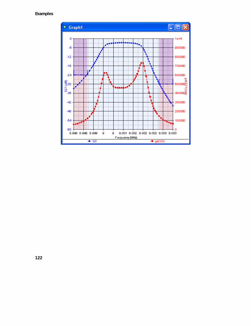
Examples
122
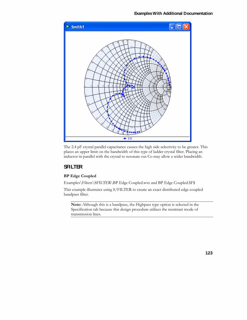
Examples With Additional Documentation
123
The 2.4 pF crystal parallel capacitance causes the high side selectivity to be greater. This places an upper limit on the bandwidth of this type of ladder crystal filter. Placing an inductor in parallel with the crystal to resonate out Co may allow a wider bandwidth.
SFILTER
BP Edge Coupled Examples\Filters\SFILTER\BP Edge Coupled.wsx and BP Edge Coupled.SF$ This example illustrates using S/FILTER to create an exact distributed edge-coupled bandpass filter.
Note: Although this is a bandpass, the Highpass type option is selected in the Specification tab because this design procedure utilizes the reentrant mode of transmission lines.
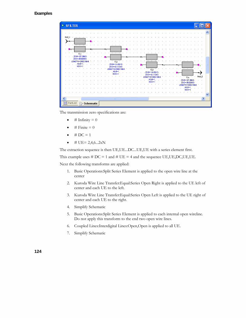
Examples
124
The transmission zero specifications are:
• # Infinity = 0
• # Finite = 0
• # DC = 1
• # UE= 2,4,6...2xN
The extraction sequence is then UE,UE...DC...UE,UE with a series element first.
This example uses # DC = 1 and # UE = 4 and the sequence UE,UE,DC,UE,UE.
Next the following transforms are applied:
1. Basic Operations:Split Series Element is applied to the open wire line at the center
2. Kuroda Wire Line Transfer:Equal:Series Open Right is applied to the UE left of center and each UE to the left.
3. Kuroda Wire Line Transfer:Equal:Series Open Left is applied to the UE right of center and each UE to the right.
4. Simplify Schematic
5. Basic Operations:Split Series Element is applied to each internal open wireline. Do not apply this transform to the end two open wire lines.
6. Coupled Lines:Interdigital Lines:Open,Open is applied to all UE.
7. Simplify Schematic
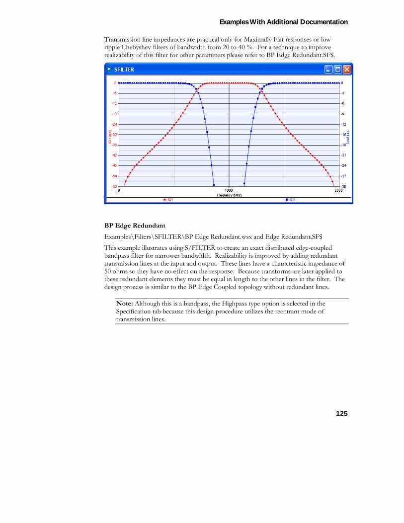
Examples With Additional Documentation
125
Transmission line impedances are practical only for Maximally Flat responses or low ripple Chebyshev filters of bandwidth from 20 to 40 %. For a technique to improve realizability of this filter for other parameters please refer to BP Edge Redundant.SF$.
BP Edge Redundant Examples\Filters\SFILTER\BP Edge Redundant.wsx and Edge Redundant.SF$ This example illustrates using S/FILTER to create an exact distributed edge-coupled bandpass filter for narrower bandwidth. Realizability is improved by adding redundant transmission lines at the input and output. These lines have a characteristic impedance of 50 ohms so they have no effect on the response. Because transforms are later applied to these redundant elements they must be equal in length to the other lines in the filter. The design process is similar to the BP Edge Coupled topology without redundant lines.
Note: Although this is a bandpass, the Highpass type option is selected in the Specification tab because this design procedure utilizes the reentrant mode of transmission lines.
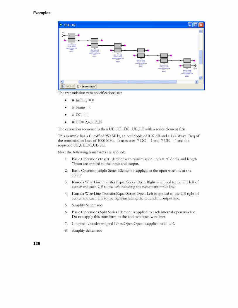
Examples
126
The transmission zero specifications are:
• # Infinity = 0
• # Finite = 0
• # DC = 1
• # UE= 2,4,6...2xN
The extraction sequence is then UE,UE...DC...UE,UE with a series element first.
This example has a Cutoff of 950 MHz, an equiripple of 0.07 dB and a 1/4 Wave Freq of the transmission lines of 1000 MHz. It uses uses # DC = 1 and # UE = 4 and the sequence UE,UE,DC,UE,UE.
Next the following transforms are applied:
1. Basic Operations:Insert Element with transmission lines = 50 ohms and length 75mm are applied to the input and output.
2. Basic Operations:Split Series Element is applied to the open wire line at the center
3. Kuroda Wire Line Transfer:Equal:Series Open Right is applied to the UE left of center and each UE to the left including the redundant input line.
4. Kuroda Wire Line Transfer:Equal:Series Open Left is applied to the UE right of center and each UE to the right including the redundant output line.
5. Simplify Schematic
6. Basic Operations:Split Series Element is applied to each internal open wireline. Do not apply this transform to the end two open wire lines.
7. Coupled Lines:Interdigital Lines:Open,Open is applied to all UE.
8. Simplify Schematic
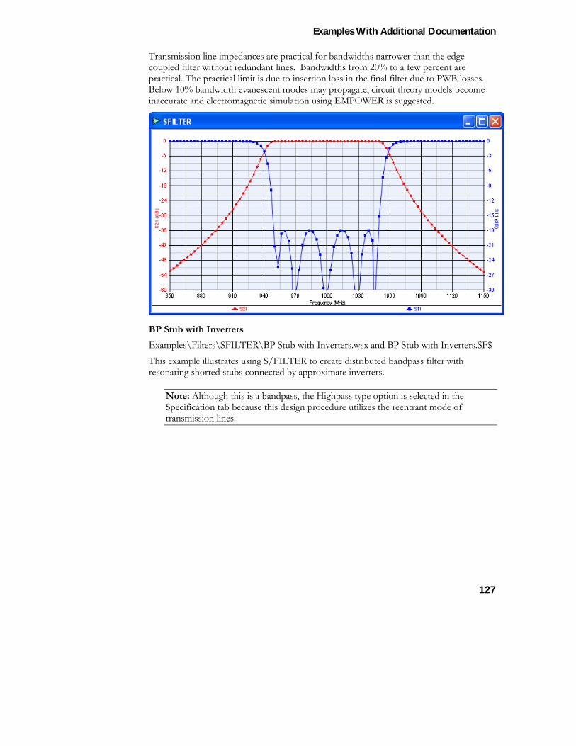
Examples With Additional Documentation
127
Transmission line impedances are practical for bandwidths narrower than the edge coupled filter without redundant lines. Bandwidths from 20% to a few percent are practical. The practical limit is due to insertion loss in the final filter due to PWB losses. Below 10% bandwidth evanescent modes may propagate, circuit theory models become inaccurate and electromagnetic simulation using EMPOWER is suggested.
BP Stub with Inverters Examples\Filters\SFILTER\BP Stub with Inverters.wsx and BP Stub with Inverters.SF$ This example illustrates using S/FILTER to create distributed bandpass filter with resonating shorted stubs connected by approximate inverters.
Note: Although this is a bandpass, the Highpass type option is selected in the Specification tab because this design procedure utilizes the reentrant mode of transmission lines.
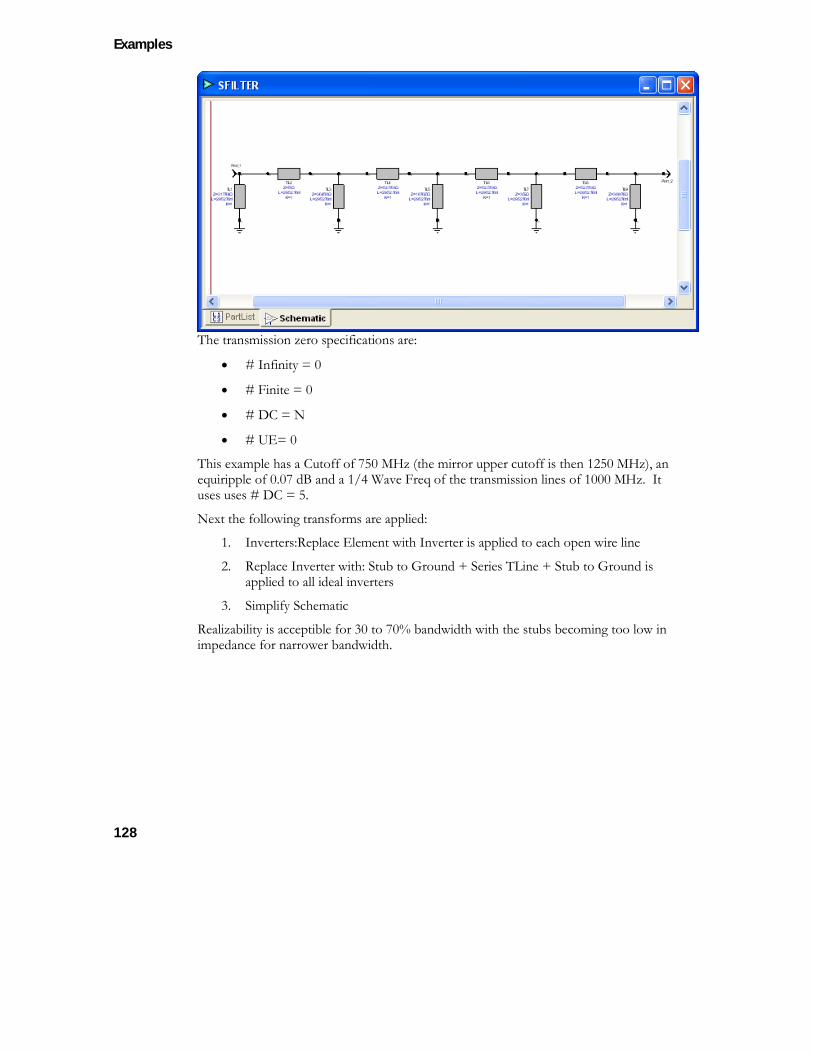
Examples
128
The transmission zero specifications are:
• # Infinity = 0
• # Finite = 0
• # DC = N
• # UE= 0
This example has a Cutoff of 750 MHz (the mirror upper cutoff is then 1250 MHz), an equiripple of 0.07 dB and a 1/4 Wave Freq of the transmission lines of 1000 MHz. It uses uses # DC = 5.
Next the following transforms are applied:
1. Inverters:Replace Element with Inverter is applied to each open wire line
2. Replace Inverter with: Stub to Ground + Series TLine + Stub to Ground is applied to all ideal inverters
3. Simplify Schematic
Realizability is acceptible for 30 to 70% bandwidth with the stubs becoming too low in impedance for narrower bandwidth.
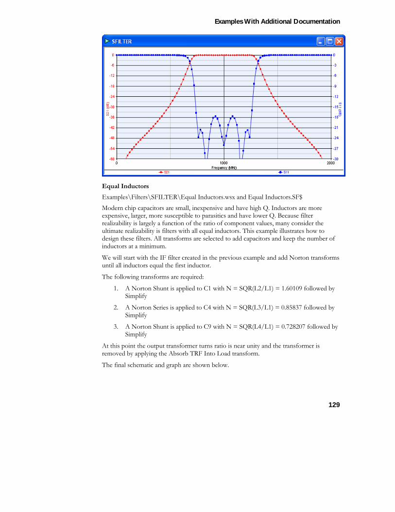
Examples With Additional Documentation
129
Equal Inductors Examples\Filters\SFILTER\Equal Inductors.wsx and Equal Inductors.SF$ Modern chip capacitors are small, inexpensive and have high Q. Inductors are more expensive, larger, more susceptible to parasitics and have lower Q. Because filter realizability is largely a function of the ratio of component values, many consider the ultimate realizability is filters with all equal inductors. This example illustrates how to design these filters. All transforms are selected to add capacitors and keep the number of inductors at a minimum.
We will start with the IF filter created in the previous example and add Norton transforms until all inductors equal the first inductor.
The following transforms are required:
1. A Norton Shunt is applied to C1 with N = SQR(L2/L1) = 1.60109 followed by Simplify
2. A Norton Series is applied to C4 with N = SQR(L3/L1) = 0.85837 followed by Simplify
3. A Norton Shunt is applied to C9 with N = SQR(L4/L1) = 0.728207 followed by Simplify
At this point the output transformer turns ratio is near unity and the transformer is removed by applying the Absorb TRF Into Load transform.
The final schematic and graph are shown below.
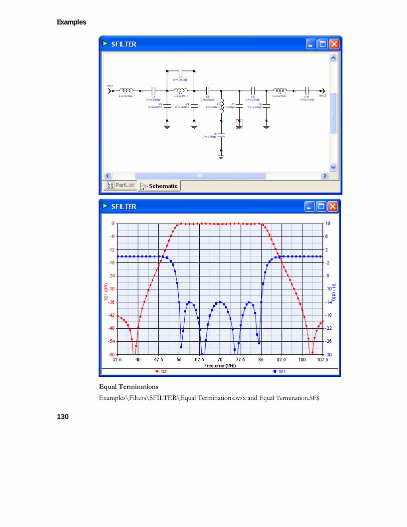
Examples
130
Equal Terminations Examples\Filters\SFILTER\Equal Terminations.wsx and Equal Termination.SF$
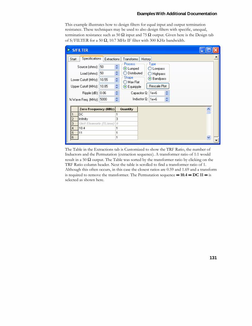
Examples With Additional Documentation
131
This example illustrates how to design filters for equal input and output termination resistance. These techniques may be used to also design filters with specific, unequal, termination resistance such as 50 Ω input and 75 Ω output. Given here is the Design tab of S/FILTER for a 50 Ω, 10.7 MHz IF filter with 300 KHz bandwidth.
The Table in the Extractions tab is Customized to show the TRF Ratio, the number of Inductors and the Permutation (extraction sequence). A transformer ratio of 1:1 would result in a 50 Ω output. The Table was sorted by the transformer ratio by clicking on the TRF Ratio column header. Next the table is scrolled to find a transformer ratio of 1. Although this often occurs, in this case the closest ratios are 0.59 and 1.69 and a transform is required to remove the transformer. The Permutation sequence ∞∞∞∞ 10.4 ∞∞∞∞ DC 11 ∞∞∞∞ is selected as shown here.
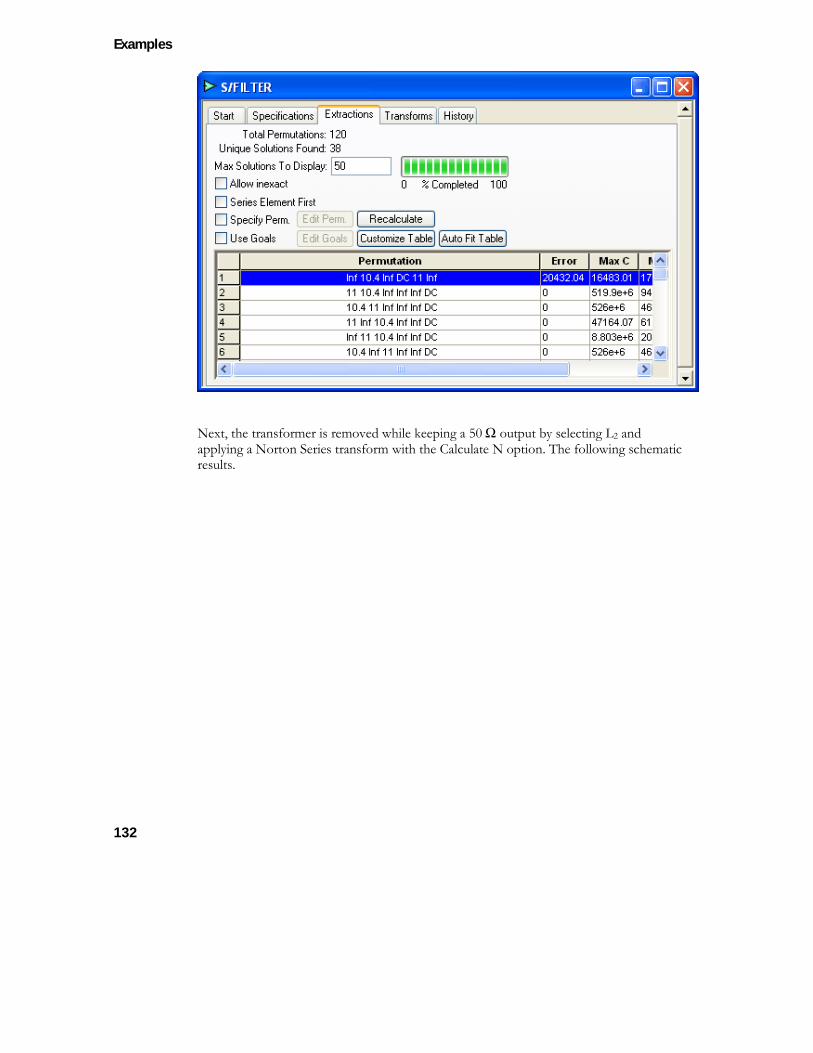
Examples
132
Next, the transformer is removed while keeping a 50 Ω output by selecting L2 and applying a Norton Series transform with the Calculate N option. The following schematic results.
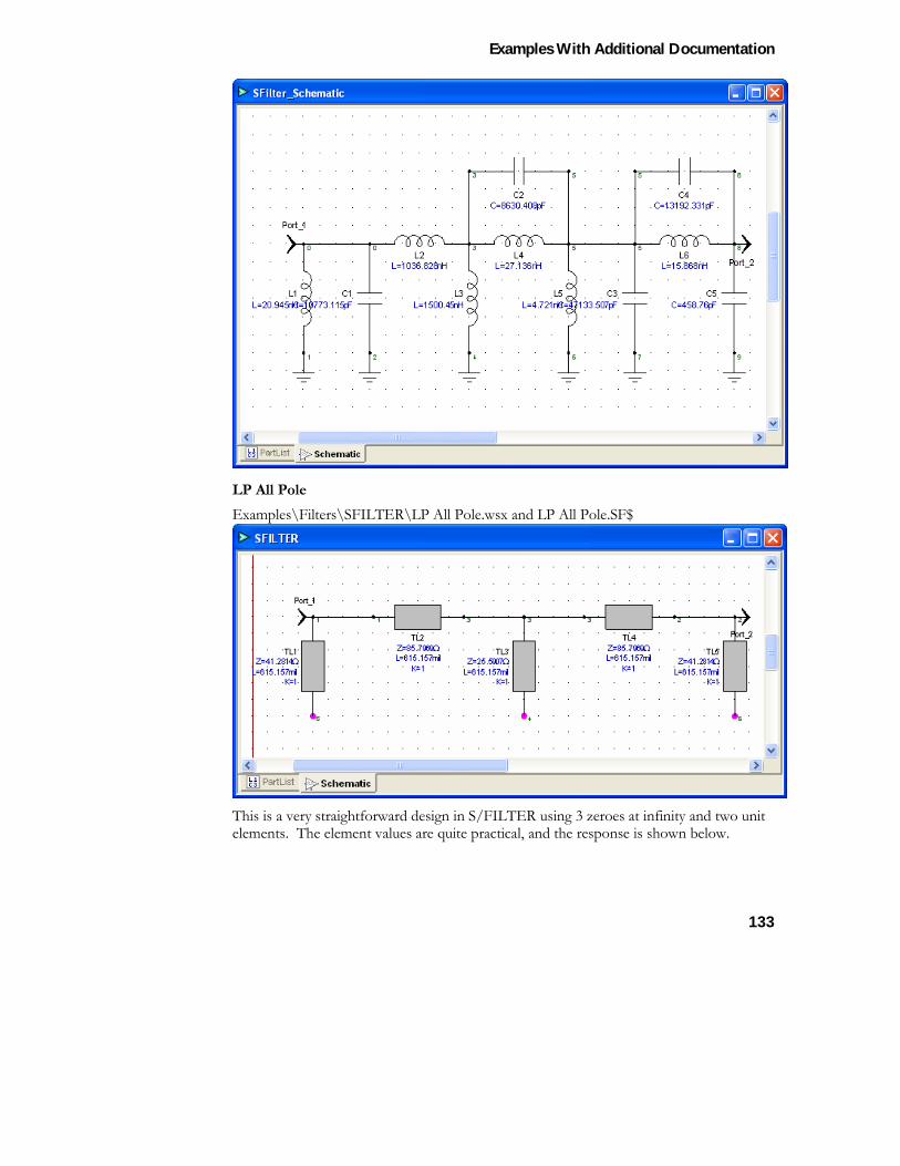
Examples With Additional Documentation
133
LP All Pole Examples\Filters\SFILTER\LP All Pole.wsx and LP All Pole.SF$
This is a very straightforward design in S/FILTER using 3 zeroes at infinity and two unit elements. The element values are quite practical, and the response is shown below.
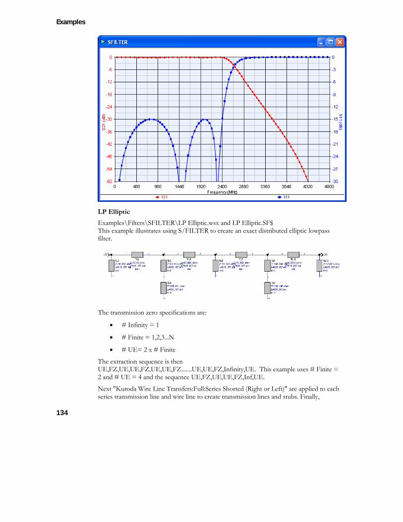
Examples
134
LP Elliptic Examples\Filters\SFILTER\LP Elliptic.wsx and LP Elliptic.SF$ This example illustrates using S/FILTER to create an exact distributed elliptic lowpass filter.
The transmission zero specifications are:
• # Infinity = 1
• # Finite = 1,2,3...N
• # UE= 2 x # Finite
The extraction sequence is then UE,FZ,UE,UE,FZ,UE,UE,FZ.......UE,UE,FZ,Infinity,UE. This example uses # Finite = 2 and # UE = 4 and the sequence UE,FZ,UE,UE,FZ,Inf,UE.
Next "Kuroda Wire Line Transfers:Full:Series Shorted (Right or Left)" are applied to each series transmission line and wire line to create transmission lines and stubs. Finally,
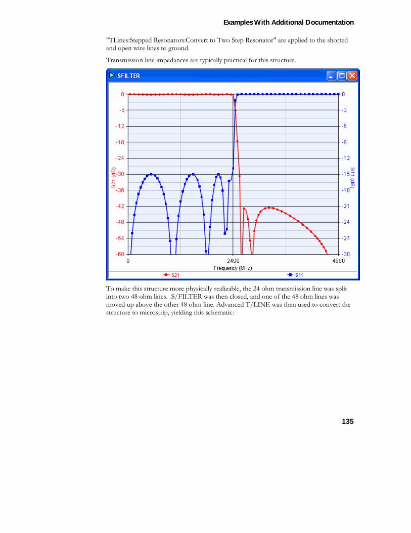
Examples With Additional Documentation
135
"TLines:Stepped Resonators:Convert to Two Step Resonator" are applied to the shorted and open wire lines to ground.
Transmission line impedances are typically practical for this structure.
To make this structure more physically realizable, the 24 ohm transmission line was split into two 48 ohm lines. S/FILTER was then closed, and one of the 48 ohm lines was moved up above the other 48 ohm line. Advanced T/LINE was then used to convert the structure to microstrip, yielding this schematic:
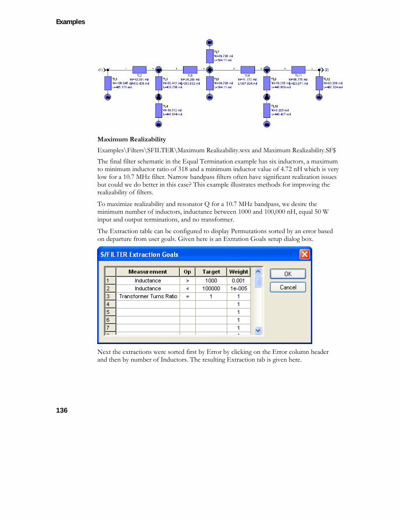
Examples
136
Maximum Realizability Examples\Filters\SFILTER\Maximum Realizability.wsx and Maximum Realizability.SF$ The final filter schematic in the Equal Termination example has six inductors, a maximum to minimum inductor ratio of 318 and a minimum inductor value of 4.72 nH which is very low for a 10.7 MHz filter. Narrow bandpass filters often have significant realization issues but could we do better in this case? This example illustrates methods for improving the realizability of filters.
To maximize realizability and resonator Q for a 10.7 MHz bandpass, we desire the minimum number of inductors, inductance between 1000 and 100,000 nH, equal 50 W input and output terminations, and no transformer.
The Extraction table can be configured to display Permutations sorted by an error based on departure from user goals. Given here is an Extration Goals setup dialog box.
Next the extractions were sorted first by Error by clicking on the Error column header and then by number of Inductors. The resulting Extraction tab is given here.
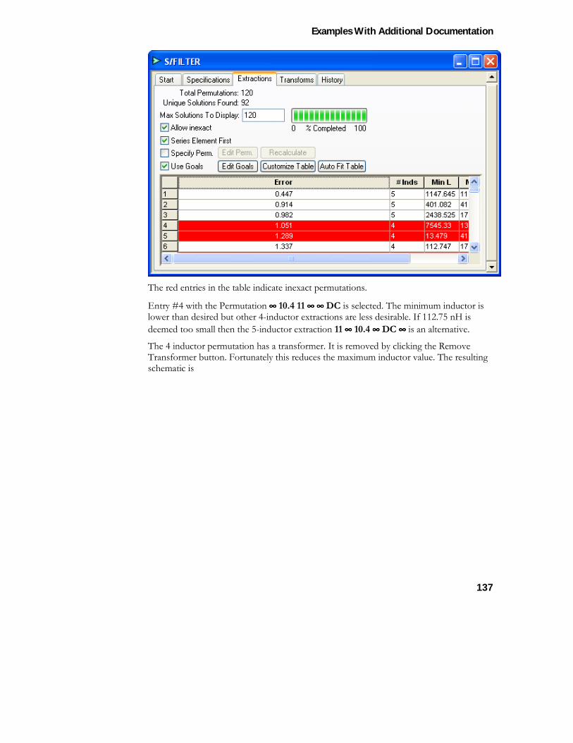
Examples With Additional Documentation
137
The red entries in the table indicate inexact permutations.
Entry #4 with the Permutation ∞∞∞∞ 10.4 11 ∞∞∞∞ ∞∞∞∞ DC is selected. The minimum inductor is lower than desired but other 4-inductor extractions are less desirable. If 112.75 nH is deemed too small then the 5-inductor extraction 11 ∞∞∞∞ 10.4 ∞∞∞∞ DC ∞∞∞∞ is an alternative.
The 4 inductor permutation has a transformer. It is removed by clicking the Remove Transformer button. Fortunately this reduces the maximum inductor value. The resulting schematic is
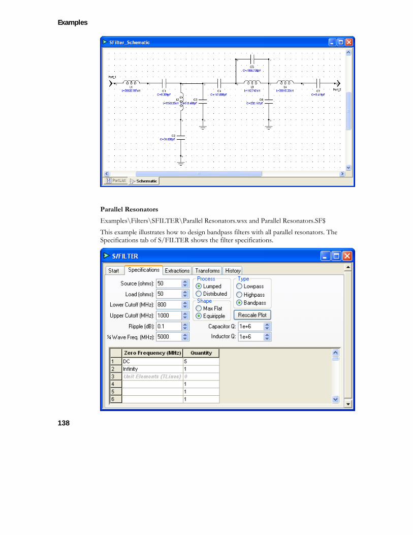
Examples
138
Parallel Resonators Examples\Filters\SFILTER\Parallel Resonators.wsx and Parallel Resonators.SF$ This example illustrates how to design bandpass filters with all parallel resonators. The Specifications tab of S/FILTER shows the filter specifications.
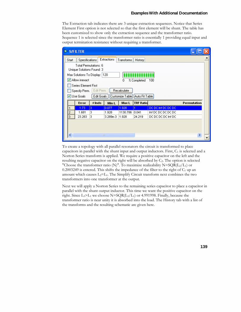
Examples With Additional Documentation
139
The Extraction tab indicates there are 3 unique extraction sequences. Notice that Series Element First option is not selected so that the first element will be shunt. The table has been customized to show only the extraction sequence and the transformer ratio. Sequence 1 is selected since the transformer ratio is essentially 1 providing equal input and output termination resistance without requiring a transformer.
To create a topology with all parallel resonators the circuit is transformed to place capacitors in parallel with the shunt input and output inductors. First, C1 is selected and a Norton Series transform is applied. We require a positive capacitor on the left and the resulting negative capacitor on the right will be absorbed by C2. The option is selected "Choose the transformer ratio (N)". To maximize realizability N=SQR(L2/L1) or 0.2003249 is entered. This shifts the impedance of the filter to the right of C1 up an amount which causes L2=L1. The Simplify Circuit transform next combines the two transformers into one transformer at the output.
Next we will apply a Norton Series to the remaining series capacitor to place a capacitor in parallel with the shunt output inductor. This time we want the positive capacitor on the right. Since L3>L1 we choose N=SQR(L3/L1) or 4.991998. Finally, because the transformer ratio is near unity it is absorbed into the load. The History tab with a list of the transforms and the resulting schematic are given here.
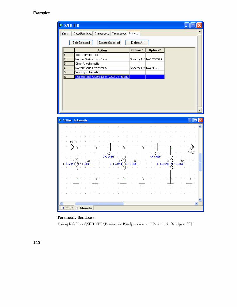
Examples
140
Parametric Bandpass Examples\Filters\SFILTER\Parametric Bandpass.wsx and Parametric Bandpass.SF$
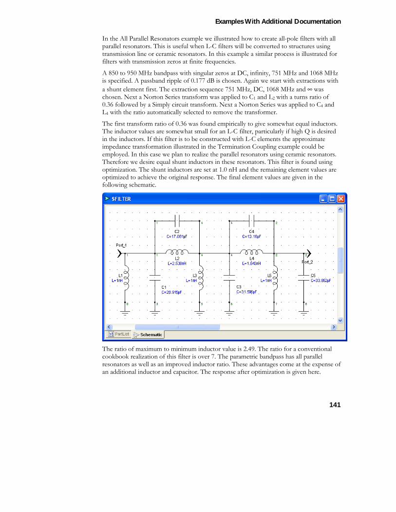
Examples With Additional Documentation
141
In the All Parallel Resonators example we illustrated how to create all-pole filters with all parallel resonators. This is useful when L-C filters will be converted to structures using transmission line or ceramic resonators. In this example a similar process is illustrated for filters with transmission zeros at finite frequencies.
A 850 to 950 MHz bandpass with singular zeros at DC, infinity, 751 MHz and 1068 MHz is specified. A passband ripple of 0.177 dB is chosen. Again we start with extractions with a shunt element first. The extraction sequence 751 MHz, DC, 1068 MHz and ∞ was chosen. Next a Norton Series transform was applied to C1 and L2 with a turns ratio of 0.36 followed by a Simply circuit transform. Next a Norton Series was applied to C4 and L4 with the ratio automatically selected to remove the transformer.
The first transform ratio of 0.36 was found empirically to give somewhat equal inductors. The inductor values are somewhat small for an L-C filter, particularly if high Q is desired in the inductors. If this filter is to be constructed with L-C elements the approximate impedance transformation illustrated in the Termination Coupling example could be employed. In this case we plan to realize the parallel resonators using ceramic resonators. Therefore we desire equal shunt inductors in these resonators. This filter is found using optimization. The shunt inductors are set at 1.0 nH and the remaining element values are optimized to achieve the original response. The final element values are given in the following schematic.
The ratio of maximum to minimum inductor value is 2.49. The ratio for a conventional cookbook realization of this filter is over 7. The parametric bandpass has all parallel resonators as well as an improved inductor ratio. These advantages come at the expense of an additional inductor and capacitor. The response after optimization is given here.
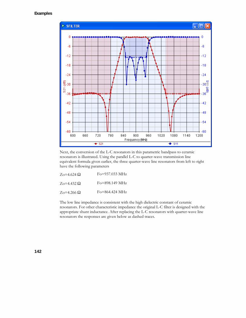
Examples
142
Next, the conversion of the L-C resonators in this parametric bandpass to ceramic resonators is illustrated. Using the parallel L-C to quarter-wave transmission line equivalent formula given earlier, the three quarter-wave line resonators from left to right have the following parameters
Zo=4.624 Ω Fo=937.033 MHz
Zo=4.432 Ω Fo=898.149 MHz
Zo=4.266 Ω Fo=864.424 MHz
The low line impedance is consistent with the high dielectric constant of ceramic resonators. For other characteristic impedance the original L-C filter is designed with the appropriate shunt inductance. After replacing the L-C resonators with quarter-wave line resonators the responses are given below as dashed traces.
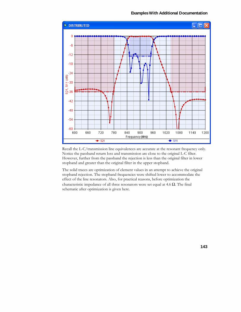
Examples With Additional Documentation
143
Recall the L-C/transmission line equivalences are accurate at the resonant frequency only. Notice the passband return loss and transmission are close to the original L-C filter. However, further from the passband the rejection is less than the original filter in lower stopband and greater than the original filter in the upper stopband.
The solid traces are optimization of element values in an attempt to achieve the original stopband rejection. The stopband frequencies were shifted lower to accommodate the effect of the line resonators. Also, for practical reasons, before optimization the characteristic impedance of all three resonators were set equal at 4.6 Ω. The final schematic after optimization is given here.
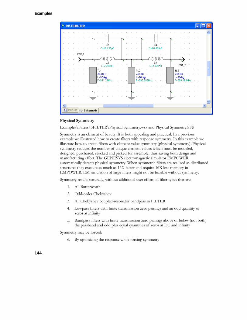
Examples
144
Physical Symmetry Examples\Filters\SFILTER\Physical Symmetry.wsx and Physical Symmetry.SF$ Symmetry is an element of beauty. It is both appealing and practical. In a previous example we illustrated how to create filters with response symmetry. In this example we illustrate how to create filters with element value symmetry (physical symmetry). Physical symmetry reduces the number of unique element values which must be modeled, designed, purchased, stocked and picked for assembly, thus saving both design and manufacturing effort. The GENESYS electromagnetic simulator EMPOWER automatically detects physical symmetry. When symmetric filters are realized as distributed structures they execute as much as 16X faster and require 16X less memory in EMPOWER. EM simulation of large filters might not be feasible without symmetry.
Symmetry results naturally, without additional user effort, in filter types that are:
1. All Butterworth
2. Odd-order Chebyshev
3. All Chebyshev coupled-resonator bandpass in FILTER
4. Lowpass filters with finite transmission zero pairings and an odd quantity of zeros at infinity
5. Bandpass filters with finite transmission zero pairings above or below (not both) the passband and odd plus equal quantities of zeros at DC and infinity
Symmetry may be forced:
6. By optimizing the response while forcing symmetry
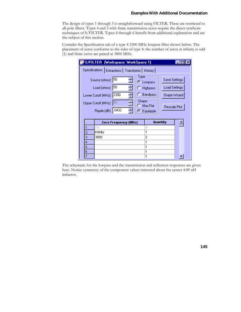
Examples With Additional Documentation
145
The design of types 1 through 3 is straightforward using FILTER. These are restricted to all-pole filters. Types 4 and 5 with finite transmission zeros require the direct synthesis techniques of S/FILTER. Types 4 through 6 benefit from additional explanation and are the subject of this section.
Consider the Specification tab of a type 4 2300 MHz lowpass filter shown below. The placement of zeros conforms to the rules of type 4: the number of zeros at infinity is odd (1) and finite zeros are paired at 3800 MHz.
The schematic for the lowpass and the transmission and reflection responses are given here. Notice symmetry of the component values mirrored about the center 4.89 nH inductor.
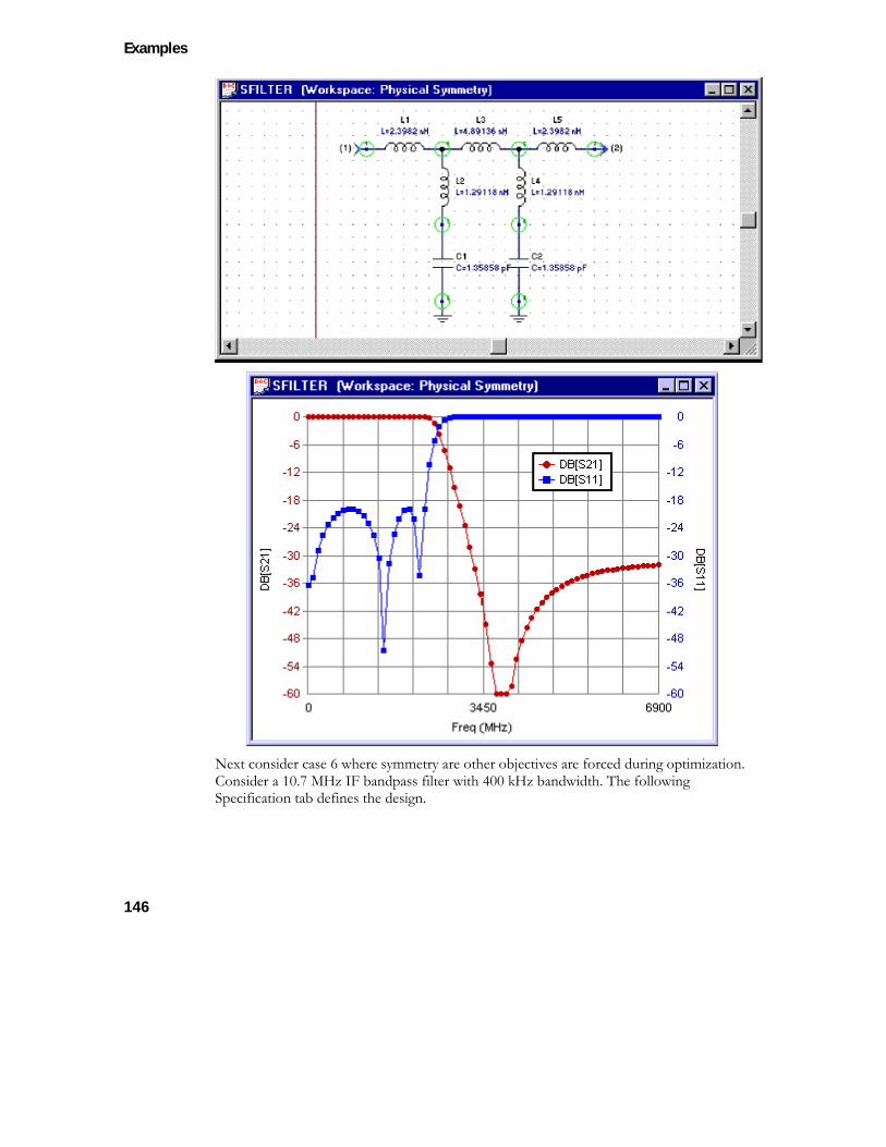
Examples
146
Next consider case 6 where symmetry are other objectives are forced during optimization. Consider a 10.7 MHz IF bandpass filter with 400 kHz bandwidth. The following Specification tab defines the design.
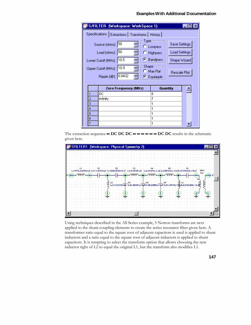
Examples With Additional Documentation
147
The extraction sequence ∞∞∞∞ DC DC DC ∞∞∞∞ ∞∞∞∞ ∞∞∞∞ ∞∞∞∞ ∞∞∞∞ ∞∞∞∞ DC DC results in the schematic given here.
Using techniques described in the All Series example, 5 Norton transforms are next applied to the shunt-coupling elements to create the series resonator filter given here. A transformer ratio equal to the square root of adjacent capacitors is used is applied to shunt inductors and a ratio equal to the square root of adjacent inductors is applied to shunt capacitors. It is tempting to select the transform option that allows choosing the new inductor right of L2 to equal the original L1, but the transform also modifies L1.
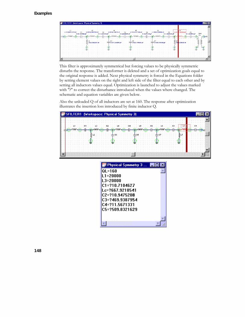
Examples
148
This filter is approximately symmetrical but forcing values to be physically symmetric disturbs the response. The transformer is deleted and a set of optimization goals equal to the original response is added. Next physical symmetry is forced in the Equations folder by setting element values on the right and left side of the filter equal to each other and by setting all inductors values equal. Optimization is launched to adjust the values marked with "?" to correct the disturbance introduced when the values where changed. The schematic and equation variables are given below.
Also the unloaded Q of all inductors are set at 160. The response after optimization illustrates the insertion loss introduced by finite inductor Q.
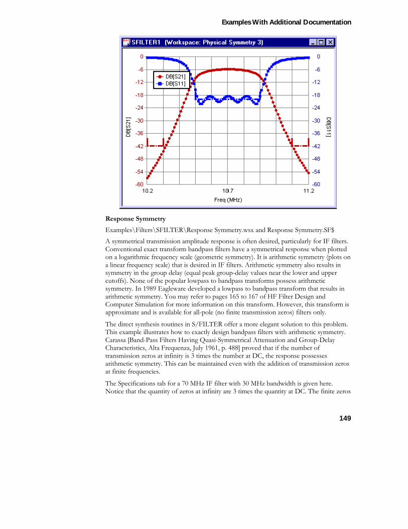
Examples With Additional Documentation
149
Response Symmetry Examples\Filters\SFILTER\Response Symmetry.wsx and Response Symmetry.SF$ A symmetrical transmission amplitude response is often desired, particularly for IF filters. Conventional exact transform bandpass filters have a symmetrical response when plotted on a logarithmic frequency scale (geometric symmetry). It is arithmetic symmetry (plots on a linear frequency scale) that is desired in IF filters. Arithmetic symmetry also results in symmetry in the group delay (equal peak group-delay values near the lower and upper cutoffs). None of the popular lowpass to bandpass transforms possess arithmetic symmetry. In 1989 Eagleware developed a lowpass to bandpass transform that results in arithmetic symmetry. You may refer to pages 165 to 167 of HF Filter Design and Computer Simulation for more information on this transform. However, this transform is approximate and is available for all-pole (no finite transmission zeros) filters only.
The direct synthesis routines in S/FILTER offer a more elegant solution to this problem. This example illustrates how to exactly design bandpass filters with arithmetic symmetry. Carassa [Band-Pass Filters Having Quasi-Symmetrical Attenuation and Group-Delay Characteristics, Alta Frequenza, July 1961, p. 488] proved that if the number of transmission zeros at infinity is 3 times the number at DC, the response possesses arithmetic symmetry. This can be maintained even with the addition of transmission zeros at finite frequencies.
The Specifications tab for a 70 MHz IF filter with 30 MHz bandwidth is given here. Notice that the quantity of zeros at infinity are 3 times the quantity at DC. The finite zeros
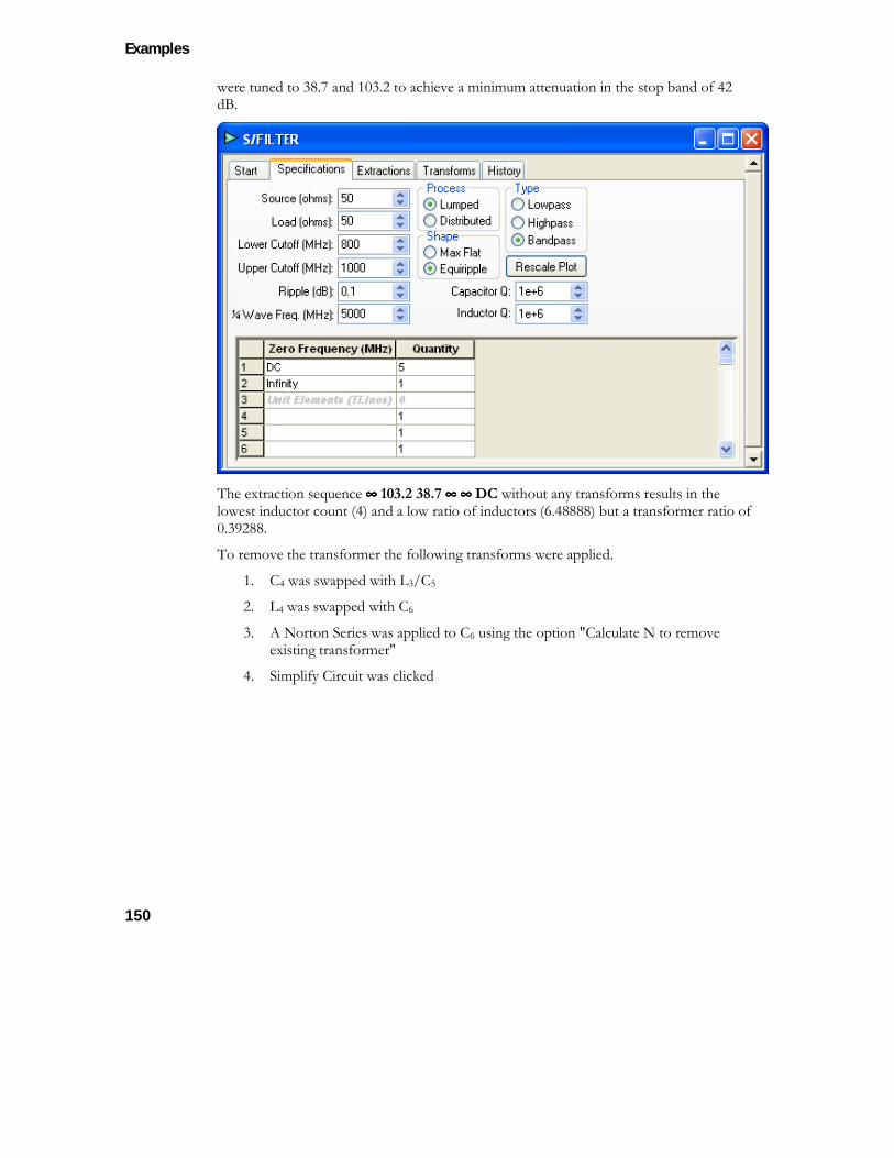
Examples
150
were tuned to 38.7 and 103.2 to achieve a minimum attenuation in the stop band of 42 dB.
The extraction sequence ∞∞∞∞ 103.2 38.7 ∞∞∞∞ ∞∞∞∞ DC without any transforms results in the lowest inductor count (4) and a low ratio of inductors (6.48888) but a transformer ratio of 0.39288.
To remove the transformer the following transforms were applied.
1. C4 was swapped with L3/C5
2. L4 was swapped with C6
3. A Norton Series was applied to C6 using the option "Calculate N to remove existing transformer"
4. Simplify Circuit was clicked
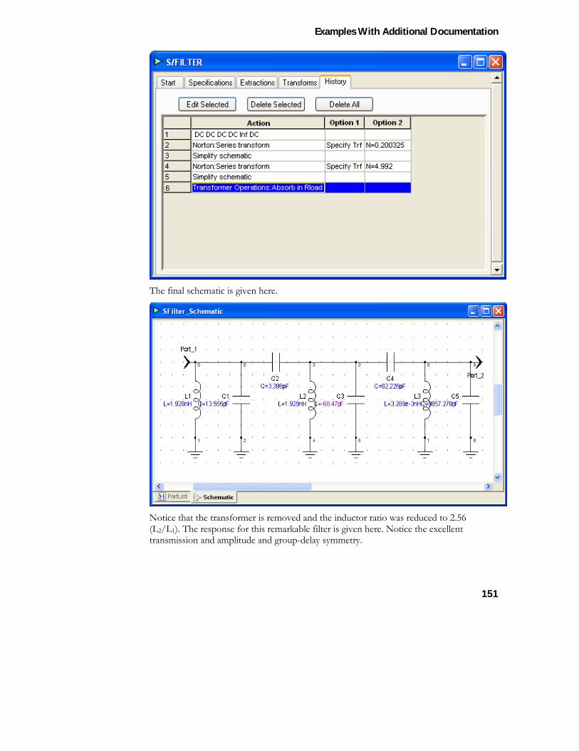
Examples With Additional Documentation
151
The final schematic is given here.
Notice that the transformer is removed and the inductor ratio was reduced to 2.56 (L2/L1). The response for this remarkable filter is given here. Notice the excellent transmission and amplitude and group-delay symmetry.
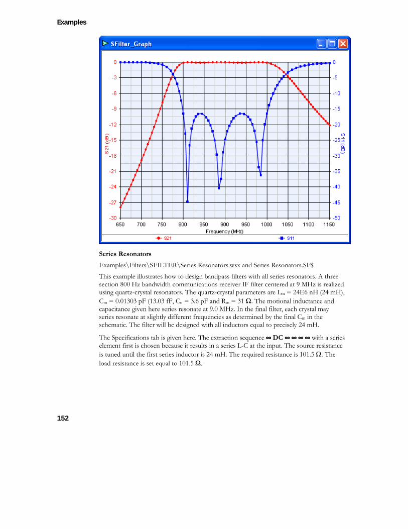
Examples
152
Series Resonators Examples\Filters\SFILTER\Series Resonators.wsx and Series Resonators.SF$ This example illustrates how to design bandpass filters with all series resonators. A three-section 800 Hz bandwidth communications receiver IF filter centered at 9 MHz is realized using quartz-crystal resonators. The quartz-crystal parameters are Lm = 24E6 nH (24 mH), Cm = 0.01303 pF (13.03 fF, Co = 3.6 pF and Rm = 31 Ω. The motional inductance and capacitance given here series resonate at 9.0 MHz. In the final filter, each crystal may series resonate at slightly different frequencies as determined by the final Cm in the schematic. The filter will be designed with all inductors equal to precisely 24 mH.
The Specifications tab is given here. The extraction sequence ∞∞∞∞ DC ∞∞∞∞ ∞∞∞∞ ∞∞∞∞ ∞∞∞∞ with a series element first is chosen because it results in a series L-C at the input. The source resistance is tuned until the first series inductor is 24 mH. The required resistance is 101.5 Ω. The load resistance is set equal to 101.5 Ω.
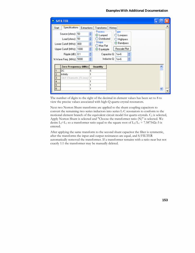
Examples With Additional Documentation
153
The number of digits to the right of the decimal in element values has been set to 8 to view the precise values associated with high-Q quartz-crystal resonators.
Next two Norton Shunt transforms are applied to the shunt coupling capacitors to convert the remaining two series inductors into series L-C resonators to conform to the motional element branch of the equivalent circuit model for quartz-crystals. C2 is selected, Apply Norton Shunt is selected and "Choose the transformer ratio (N)" is selected. We desire L2=L1 so a transformer ratio equal to the square root of L2/L1 = 7.587542e-5 is entered.
After applying the same transform to the second shunt capacitor the filter is symmetric, after the transforms the input and output resistances are equal, and S/FILTER automatically removed the transformer. If a transformer remains with a ratio near but not exactly 1:1 the transformer may be manually deleted.
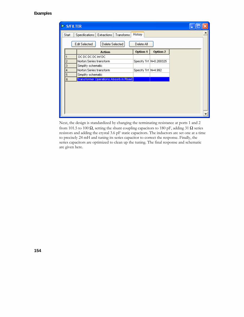
Examples
154
Next, the design is standardized by changing the terminating resistance at ports 1 and 2 from 101.5 to 100 Ω, setting the shunt coupling capacitors to 180 pF, adding 31 Ω series resistors and adding the crystal 3.6 pF static capacitors. The inductors are set one at a time to precisely 24 mH and tuning its series capacitor to correct the response. Finally, the series capacitors are optimized to clean up the tuning. The final response and schematic are given here.
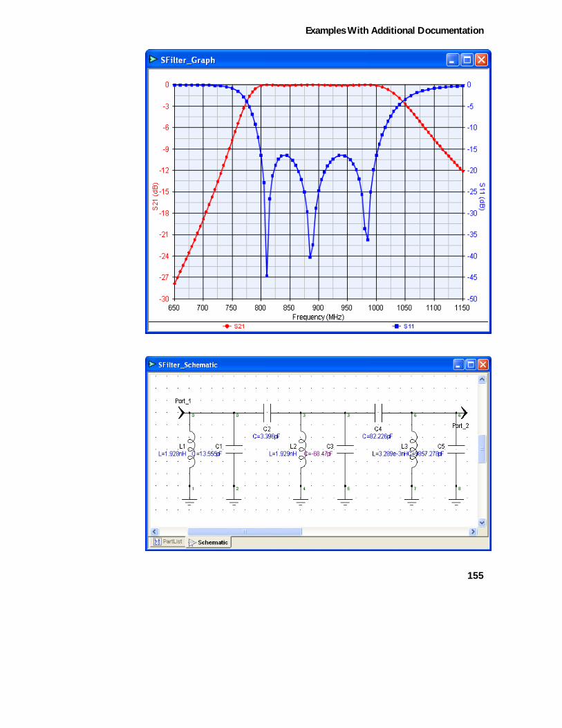
Examples With Additional Documentation
155
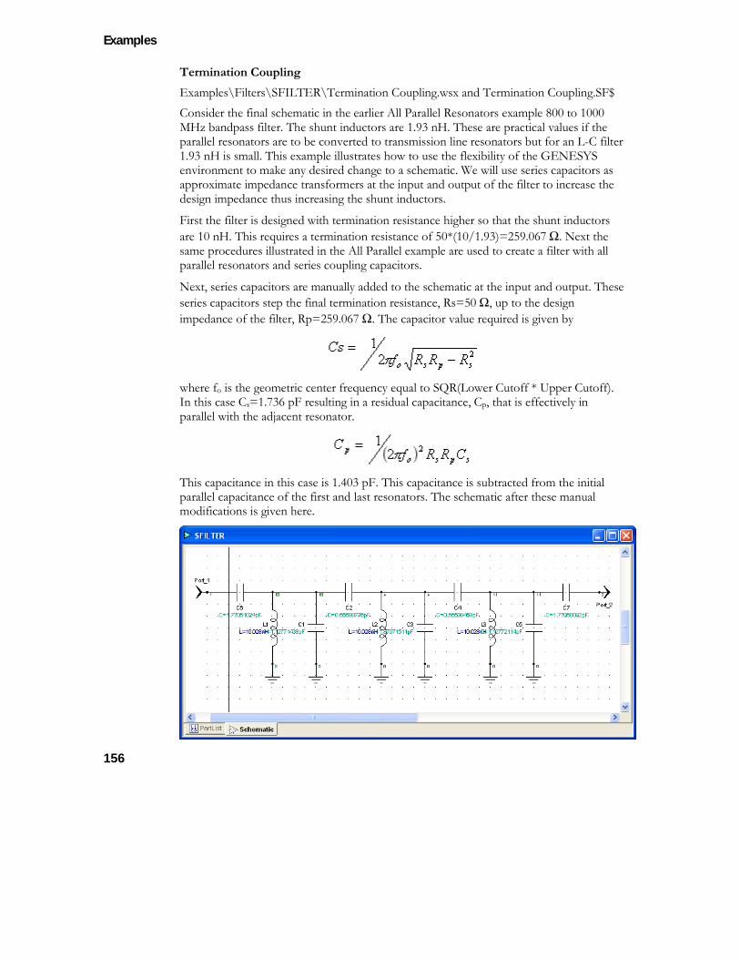
Examples
156
Termination Coupling Examples\Filters\SFILTER\Termination Coupling.wsx and Termination Coupling.SF$ Consider the final schematic in the earlier All Parallel Resonators example 800 to 1000 MHz bandpass filter. The shunt inductors are 1.93 nH. These are practical values if the parallel resonators are to be converted to transmission line resonators but for an L-C filter 1.93 nH is small. This example illustrates how to use the flexibility of the GENESYS environment to make any desired change to a schematic. We will use series capacitors as approximate impedance transformers at the input and output of the filter to increase the design impedance thus increasing the shunt inductors.
First the filter is designed with termination resistance higher so that the shunt inductors are 10 nH. This requires a termination resistance of 50*(10/1.93)=259.067 Ω. Next the same procedures illustrated in the All Parallel example are used to create a filter with all parallel resonators and series coupling capacitors.
Next, series capacitors are manually added to the schematic at the input and output. These series capacitors step the final termination resistance, Rs=50 Ω, up to the design impedance of the filter, Rp=259.067 Ω. The capacitor value required is given by
where fo is the geometric center frequency equal to SQR(Lower Cutoff * Upper Cutoff). In this case Cs=1.736 pF resulting in a residual capacitance, Cp, that is effectively in parallel with the adjacent resonator.
This capacitance in this case is 1.403 pF. This capacitance is subtracted from the initial parallel capacitance of the first and last resonators. The schematic after these manual modifications is given here.
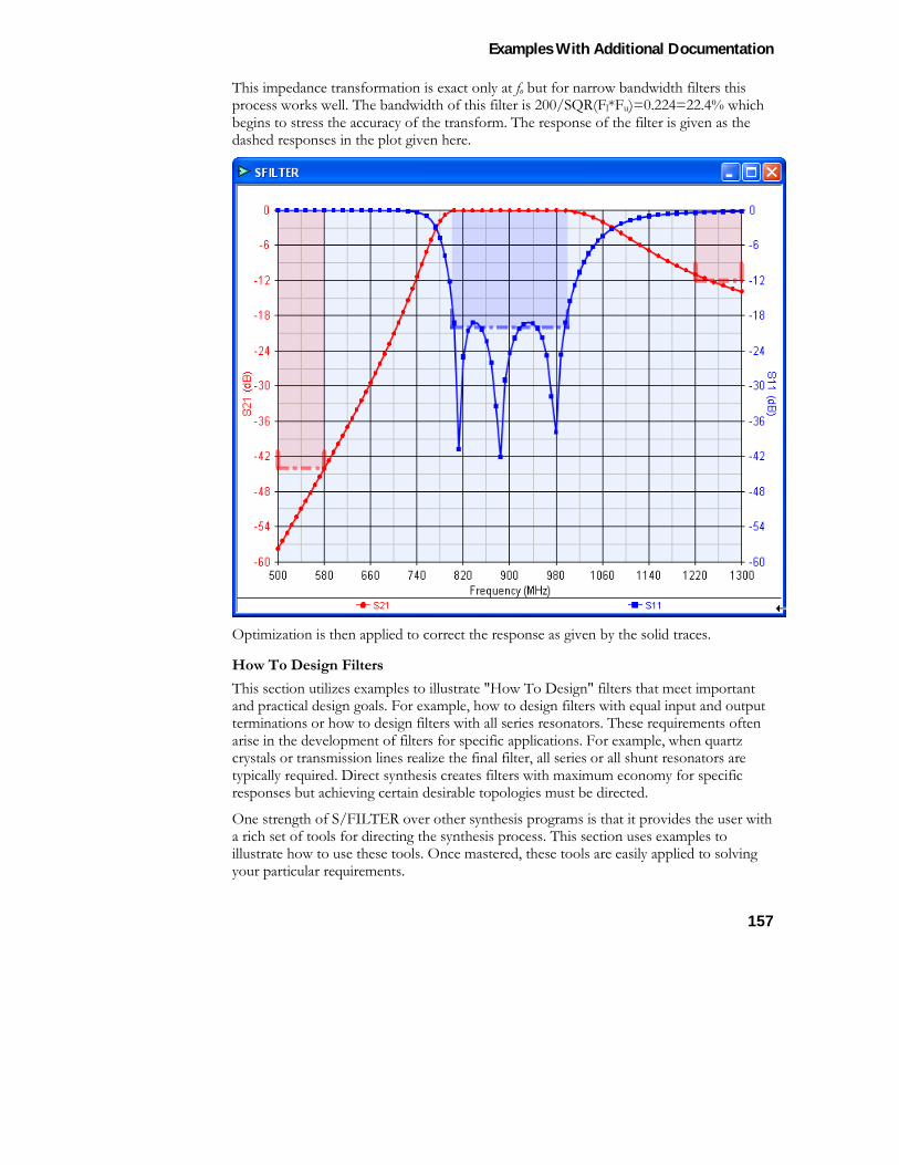
Examples With Additional Documentation
157
This impedance transformation is exact only at fo but for narrow bandwidth filters this process works well. The bandwidth of this filter is 200/SQR(Fl*Fu)=0.224=22.4% which begins to stress the accuracy of the transform. The response of the filter is given as the dashed responses in the plot given here.
Optimization is then applied to correct the response as given by the solid traces.
How To Design Filters This section utilizes examples to illustrate "How To Design" filters that meet important and practical design goals. For example, how to design filters with equal input and output terminations or how to design filters with all series resonators. These requirements often arise in the development of filters for specific applications. For example, when quartz crystals or transmission lines realize the final filter, all series or all shunt resonators are typically required. Direct synthesis creates filters with maximum economy for specific responses but achieving certain desirable topologies must be directed.
One strength of S/FILTER over other synthesis programs is that it provides the user with a rich set of tools for directing the synthesis process. This section uses examples to illustrate how to use these tools. Once mastered, these tools are easily applied to solving your particular requirements.
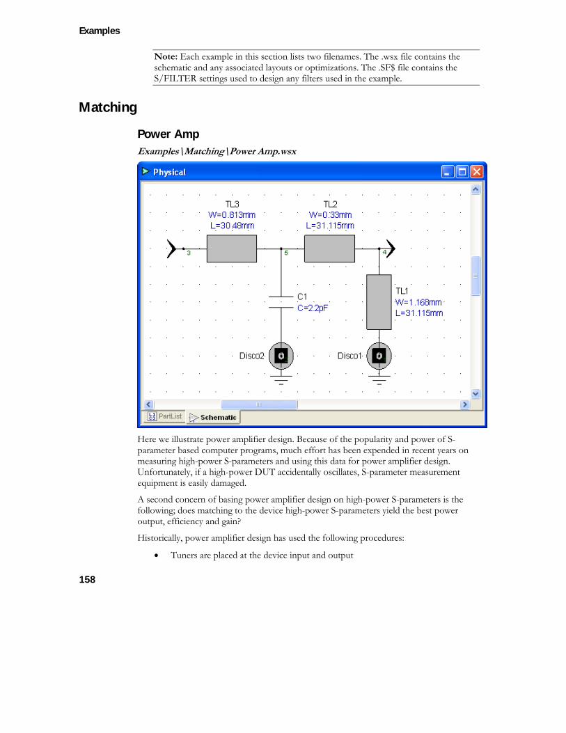
Examples
158
Note: Each example in this section lists two filenames. The .wsx file contains the schematic and any associated layouts or optimizations. The .SF$ file contains the S/FILTER settings used to design any filters used in the example.
Matching
Power Amp Examples\Matching\Power Amp.wsx
Here we illustrate power amplifier design. Because of the popularity and power of S-parameter based computer programs, much effort has been expended in recent years on measuring high-power S-parameters and using this data for power amplifier design. Unfortunately, if a high-power DUT accidentally oscillates, S-parameter measurement equipment is easily damaged.
A second concern of basing power amplifier design on high-power S-parameters is the following; does matching to the device high-power S-parameters yield the best power output, efficiency and gain?
Historically, power amplifier design has used the following procedures:
• Tuners are placed at the device input and output
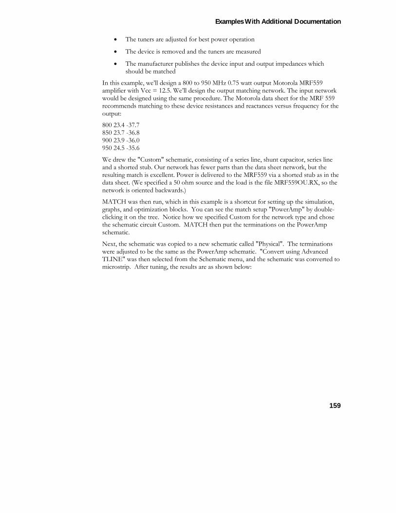
Examples With Additional Documentation
159
• The tuners are adjusted for best power operation
• The device is removed and the tuners are measured
• The manufacturer publishes the device input and output impedances which should be matched
In this example, we’ll design a 800 to 950 MHz 0.75 watt output Motorola MRF559 amplifier with Vcc = 12.5. We’ll design the output matching network. The input network would be designed using the same procedure. The Motorola data sheet for the MRF 559 recommends matching to these device resistances and reactances versus frequency for the output:
800 23.4 -37.7 850 23.7 -36.8 900 23.9 -36.0 950 24.5 -35.6
We drew the "Custom" schematic, consisting of a series line, shunt capacitor, series line and a shorted stub. Our network has fewer parts than the data sheet network, but the resulting match is excellent. Power is delivered to the MRF559 via a shorted stub as in the data sheet. (We specified a 50 ohm source and the load is the file MRF559OU.RX, so the network is oriented backwards.)
MATCH was then run, which in this example is a shortcut for setting up the simulation, graphs, and optimization blocks. You can see the match setup "PowerAmp" by double-clicking it on the tree. Notice how we specified Custom for the network type and chose the schematic circuit Custom. MATCH then put the terminations on the PowerAmp schematic.
Next, the schematic was copied to a new schematic called "Physical". The terminations were adjusted to be the same as the PowerAmp schematic. "Convert using Advanced TLINE" was then selected from the Schematic menu, and the schematic was converted to microstrip. After tuning, the results are as shown below:
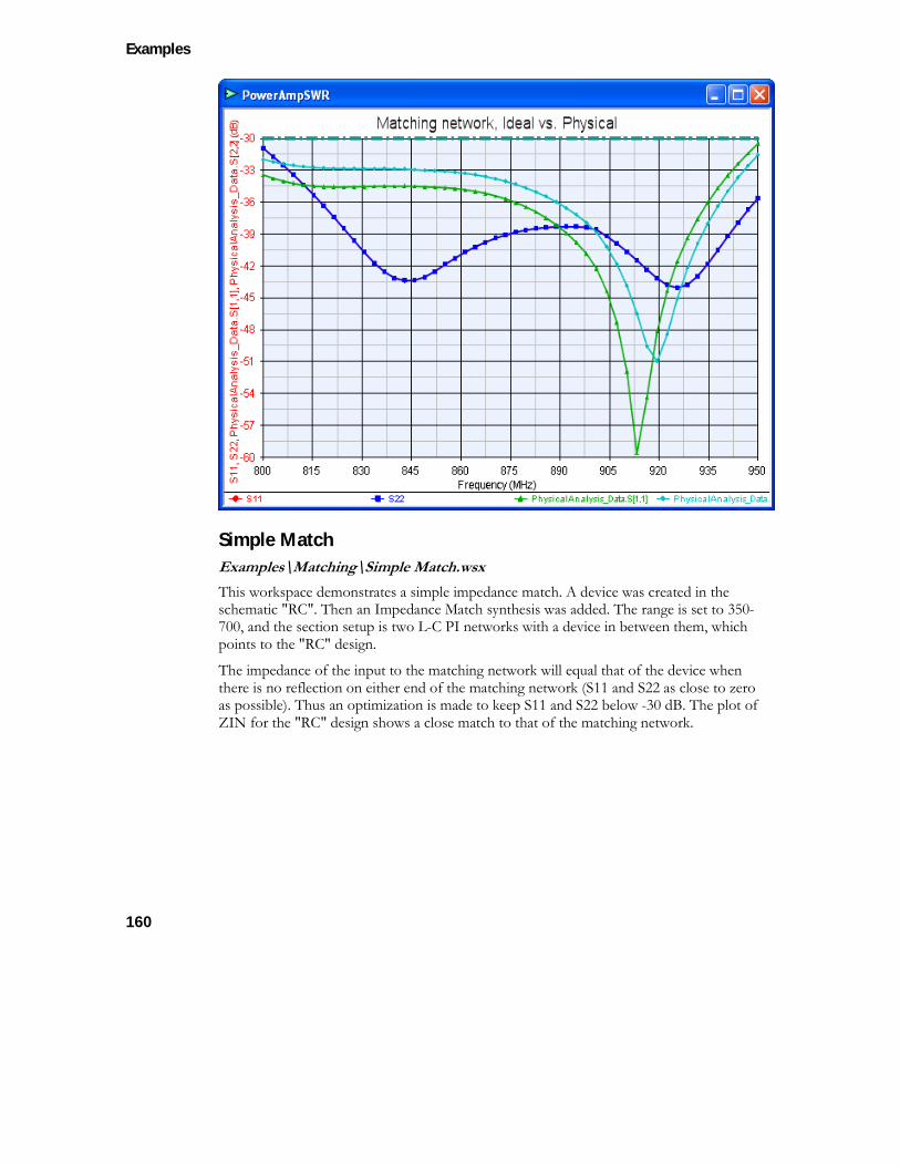
Examples
160
Simple Match Examples\Matching\Simple Match.wsx This workspace demonstrates a simple impedance match. A device was created in the schematic "RC". Then an Impedance Match synthesis was added. The range is set to 350-700, and the section setup is two L-C PI networks with a device in between them, which points to the "RC" design.
The impedance of the input to the matching network will equal that of the device when there is no reflection on either end of the matching network (S11 and S22 as close to zero as possible). Thus an optimization is made to keep S11 and S22 below -30 dB. The plot of ZIN for the "RC" design shows a close match to that of the matching network.
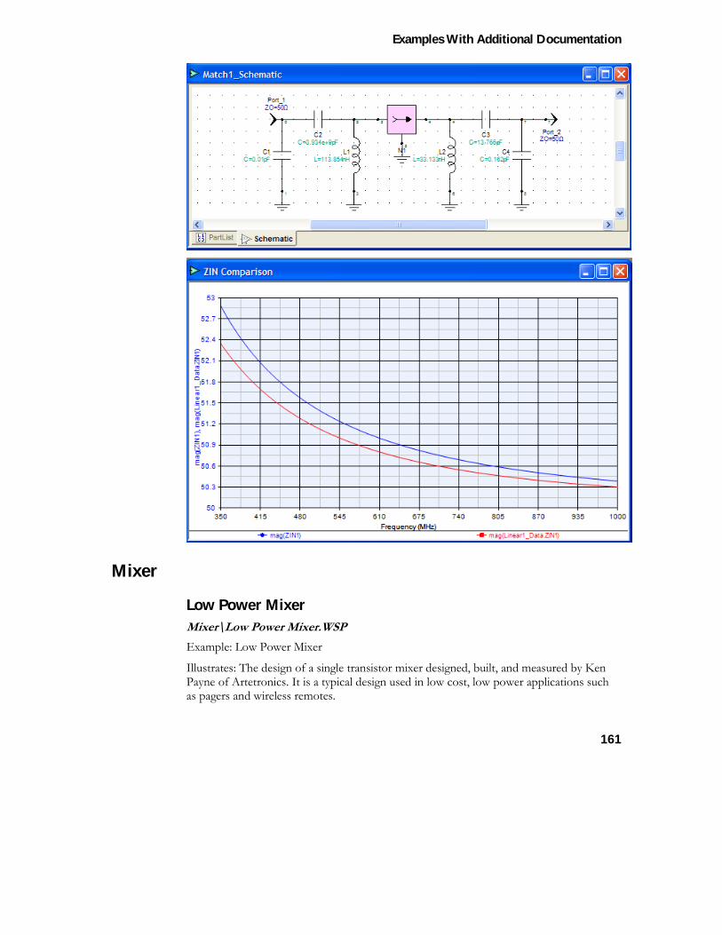
Examples With Additional Documentation
161
Mixer
Low Power Mixer Mixer\Low Power Mixer.WSP Example: Low Power Mixer
Illustrates: The design of a single transistor mixer designed, built, and measured by Ken Payne of Artetronics. It is a typical design used in low cost, low power applications such as pagers and wireless remotes.
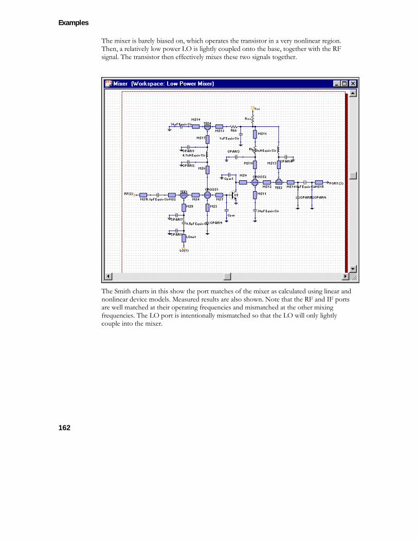
Examples
162
The mixer is barely biased on, which operates the transistor in a very nonlinear region. Then, a relatively low power LO is lightly coupled onto the base, together with the RF signal. The transistor then effectively mixes these two signals together.
The Smith charts in this show the port matches of the mixer as calculated using linear and nonlinear device models. Measured results are also shown. Note that the RF and IF ports are well matched at their operating frequencies and mismatched at the other mixing frequencies. The LO port is intentionally mismatched so that the LO will only lightly couple into the mixer.
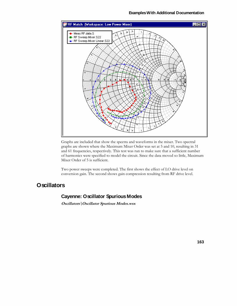
Examples With Additional Documentation
163
Graphs are included that show the spectra and waveforms in the mixer. Two spectral graphs are shown where the Maximum Mixer Order was set at 5 and 10, resulting in 31 and 61 frequencies, respectively. This test was run to make sure that a sufficient number of harmonics were specified to model the circuit. Since the data moved so little, Maximum Mixer Order of 5 is sufficient. Two power sweeps were completed. The first shows the effect of LO drive level on conversion gain. The second shows gain compression resulting from RF drive level.
Oscillators
Cayenne: Oscillator Spurious Modes Oscillators\Oscillator Spurious Modes.wsx
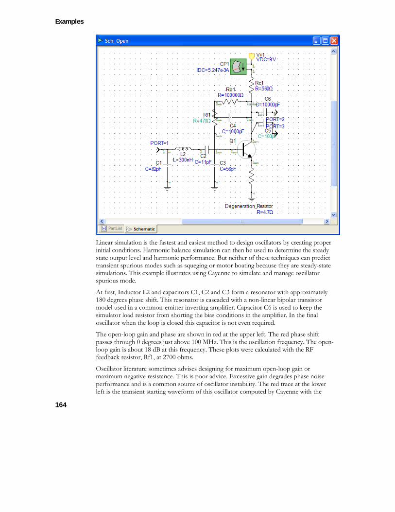
Examples
164
Linear simulation is the fastest and easiest method to design oscillators by creating proper initial conditions. Harmonic balance simulation can then be used to determine the steady state output level and harmonic performance. But neither of these techniques can predict transient spurious modes such as squeging or motor boating because they are steady-state simulations. This example illustrates using Cayenne to simulate and manage oscillator spurious mode.
At first, Inductor L2 and capacitors C1, C2 and C3 form a resonator with approximately 180 degrees phase shift. This resonator is cascaded with a non-linear bipolar transistor model used in a common-emitter inverting amplifier. Capacitor C6 is used to keep the simulator load resistor from shorting the bias conditions in the amplifier. In the final oscillator when the loop is closed this capacitor is not even required.
The open-loop gain and phase are shown in red at the upper left. The red phase shift passes through 0 degrees just above 100 MHz. This is the oscillation frequency. The open-loop gain is about 18 dB at this frequency. These plots were calculated with the RF feedback resistor, Rf1, at 2700 ohms.
Oscillator literature sometimes advises designing for maximum open-loop gain or maximum negative resistance. This is poor advice. Excessive gain degrades phase noise performance and is a common source of oscillator instability. The red trace at the lower left is the transient starting waveform of this oscillator computed by Cayenne with the

Examples With Additional Documentation
165
loop closed, as shown in the schematic at the upper right. Notice after an initial start at about 100 nS, the waveform begins to die at about 300 nS and has completely died at 750 nS, and then it restarts. The result is both AM and some FM modulation of the oscillator output spectrum with a period of 750-100 nS, or 650 nS. This is about 1.5 MHz and would be disastrous in most oscillator applications.
Next Rf1 is reduced to 270 ohms. The additional shunt resistive feedback reduces the open-loop gain at the zero crossing to about 8 dB as shown in green at the upper left. Notice the starting waveform shown in green at the lower left does not die and restart. Unfortunately, the phase slope at the zero crossing is reduced. This lower loaded Q will result in poorer oscillator phase noise and long term stability. This is shown with the _Two data sets (blue).
Third, the input and output impedance of the amplifier were better controlled increasing Rf1 to 470 ohms and adding a 4.7 ohm emitter degeneration resistor. In addition, the output coupling capacitor, C5, was reduced to 100 pF. The time constant and behavior of spurious modes are influenced by capacitors in the circuit. Small value capacitors help prevent spurious modes. Notice with these changes the gain is moderate, the phase slope was increased and the starting characteristics are much improved. This is shown in the _Three data sets (green).
It is suggested to design for about 3 to 8 dB of open loop gain. Low gain results in better phase noise and lower harmonics. Designing with low gain requires well controlled and predictable amplifier gain or the circuit may not oscillate over temperature or device to device. Higher gain offers faster starting and higher output power.
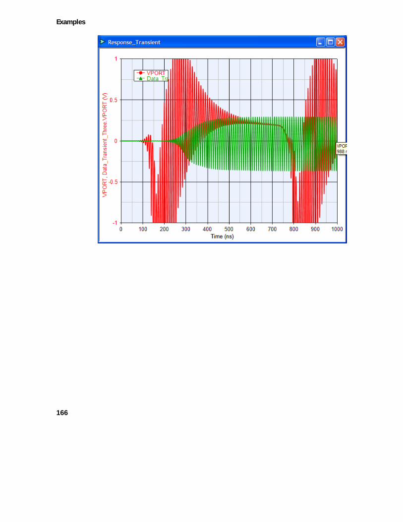
Examples
166
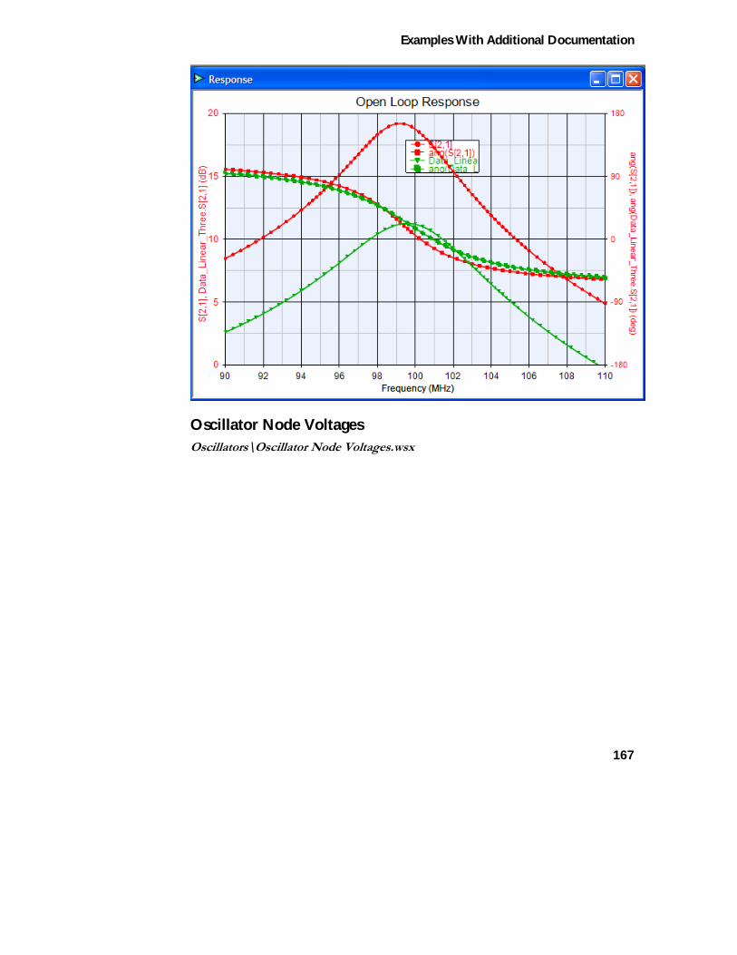
Examples With Additional Documentation
167
Oscillator Node Voltages Oscillators\Oscillator Node Voltages.wsx
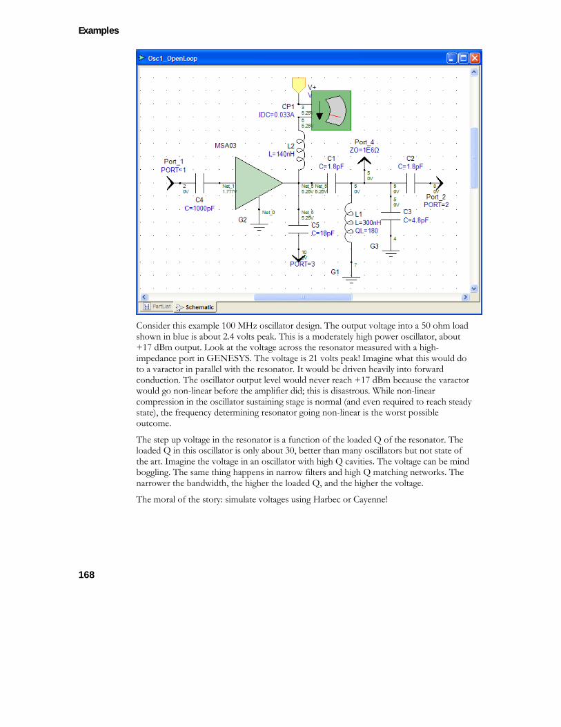
Examples
168
Consider this example 100 MHz oscillator design. The output voltage into a 50 ohm load shown in blue is about 2.4 volts peak. This is a moderately high power oscillator, about +17 dBm output. Look at the voltage across the resonator measured with a high-impedance port in GENESYS. The voltage is 21 volts peak! Imagine what this would do to a varactor in parallel with the resonator. It would be driven heavily into forward conduction. The oscillator output level would never reach +17 dBm because the varactor would go non-linear before the amplifier did; this is disastrous. While non-linear compression in the oscillator sustaining stage is normal (and even required to reach steady state), the frequency determining resonator going non-linear is the worst possible outcome.
The step up voltage in the resonator is a function of the loaded Q of the resonator. The loaded Q in this oscillator is only about 30, better than many oscillators but not state of the art. Imagine the voltage in an oscillator with high Q cavities. The voltage can be mind boggling. The same thing happens in narrow filters and high Q matching networks. The narrower the bandwidth, the higher the loaded Q, and the higher the voltage.
The moral of the story: simulate voltages using Harbec or Cayenne!
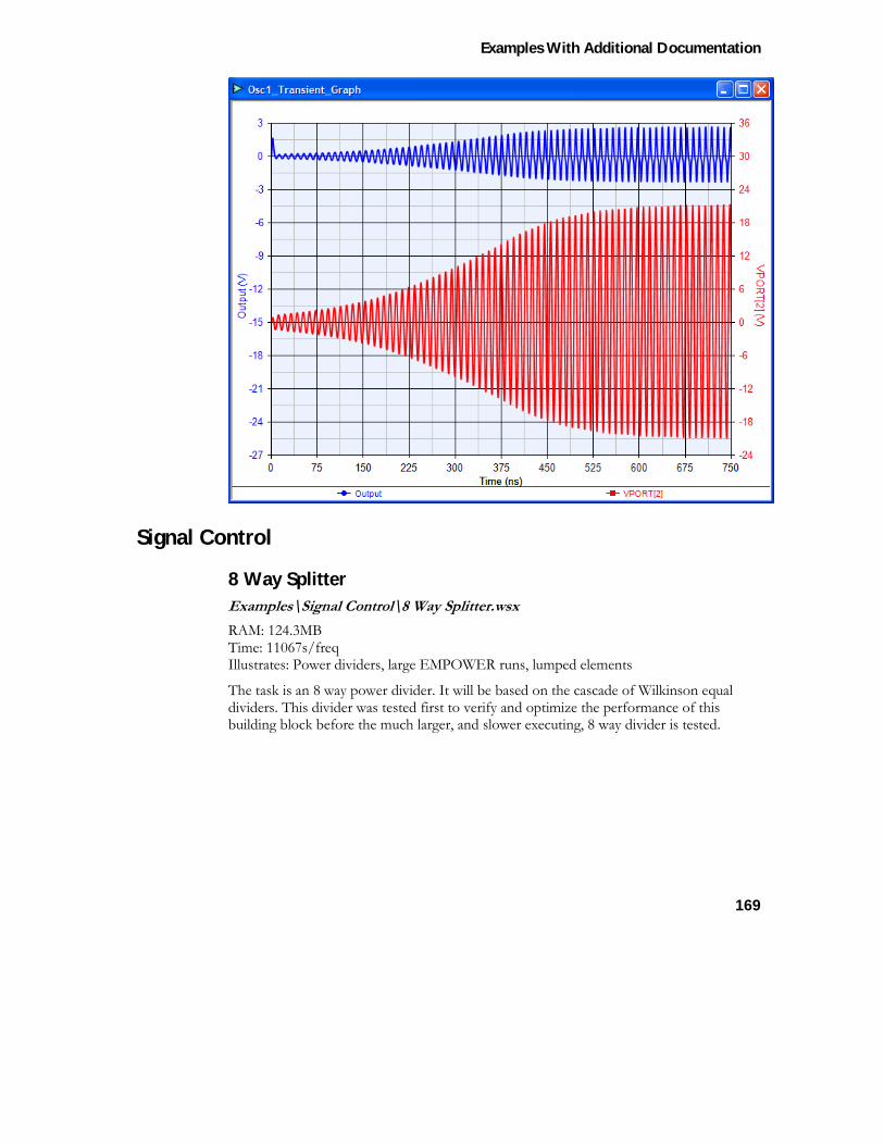
Examples With Additional Documentation
169
Signal Control
8 Way Splitter Examples\Signal Control\8 Way Splitter.wsx RAM: 124.3MB Time: 11067s/freq Illustrates: Power dividers, large EMPOWER runs, lumped elements
The task is an 8 way power divider. It will be based on the cascade of Wilkinson equal dividers. This divider was tested first to verify and optimize the performance of this building block before the much larger, and slower executing, 8 way divider is tested.
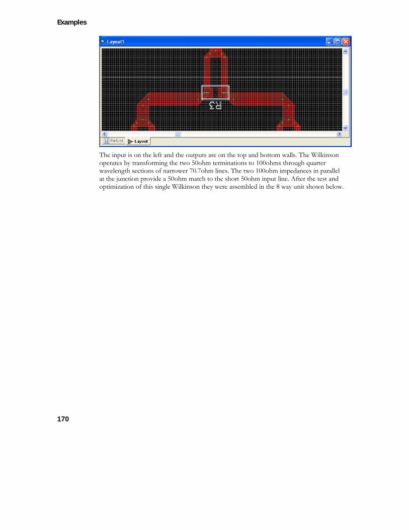
Examples
170
The input is on the left and the outputs are on the top and bottom walls. The Wilkinson operates by transforming the two 50ohm terminations to 100ohms through quarter wavelength sections of narrower 70.7ohm lines. The two 100ohm impedances in parallel at the junction provide a 50ohm match to the short 50ohm input line. After the test and optimization of this single Wilkinson they were assembled in the 8 way unit shown below.
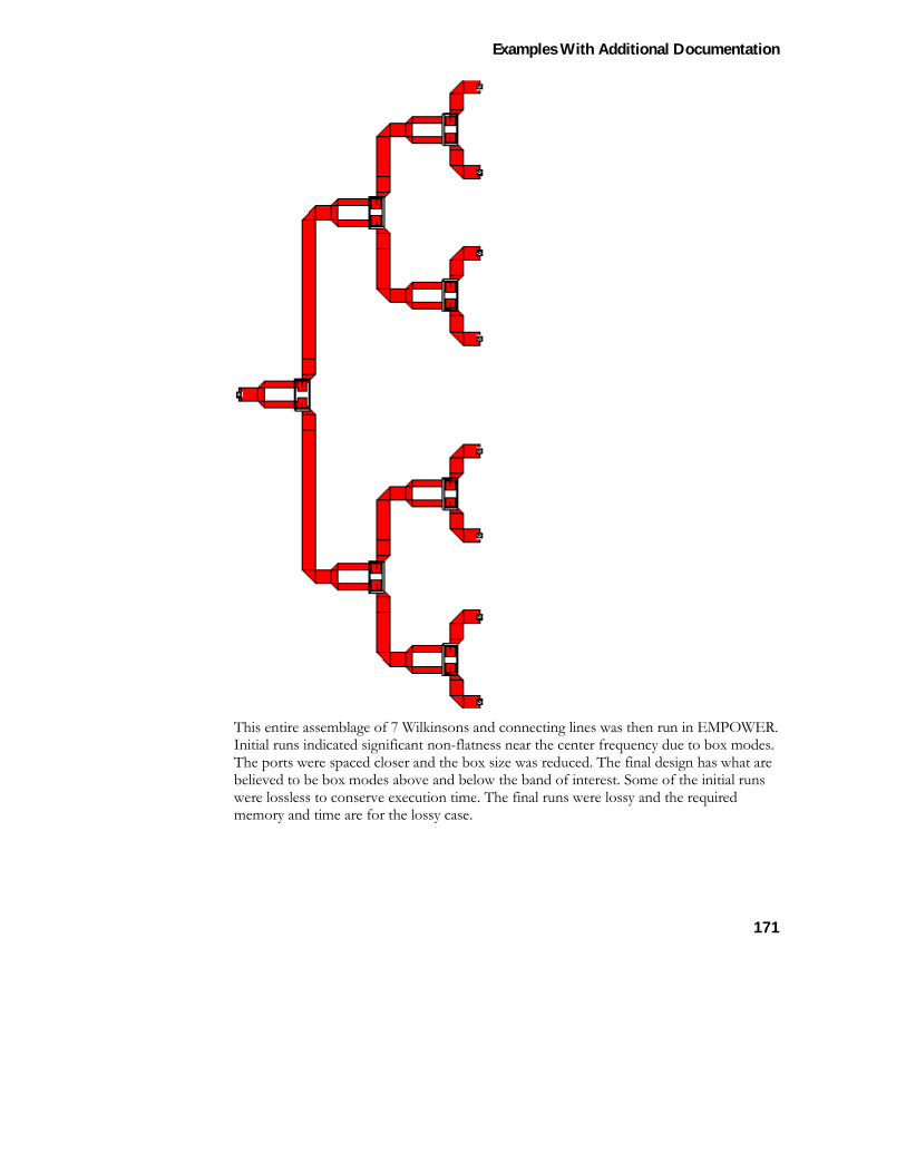
Examples With Additional Documentation
171
This entire assemblage of 7 Wilkinsons and connecting lines was then run in EMPOWER. Initial runs indicated significant non-flatness near the center frequency due to box modes. The ports were spaced closer and the box size was reduced. The final design has what are believed to be box modes above and below the band of interest. Some of the initial runs were lossless to conserve execution time. The final runs were lossy and the required memory and time are for the lossy case.
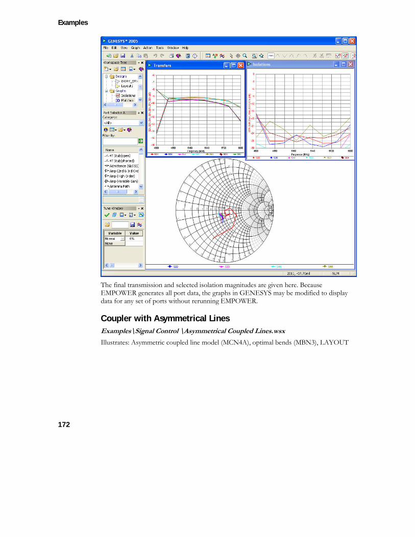
Examples
172
The final transmission and selected isolation magnitudes are given here. Because EMPOWER generates all port data, the graphs in GENESYS may be modified to display data for any set of ports without rerunning EMPOWER.
Coupler with Asymmetrical Lines Examples\Signal Control \Asymmetrical Coupled Lines.wsx Illustrates: Asymmetric coupled line model (MCN4A), optimal bends (MBN3), LAYOUT
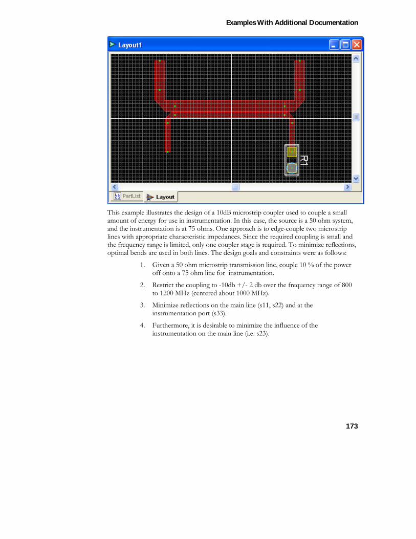
Examples With Additional Documentation
173
This example illustrates the design of a 10dB microstrip coupler used to couple a small amount of energy for use in instrumentation. In this case, the source is a 50 ohm system, and the instrumentation is at 75 ohms. One approach is to edge-couple two microstrip lines with appropriate characteristic impedances. Since the required coupling is small and the frequency range is limited, only one coupler stage is required. To minimize reflections, optimal bends are used in both lines. The design goals and constraints were as follows:
1. Given a 50 ohm microstrip transmission line, couple 10 % of the power off onto a 75 ohm line for instrumentation.
2. Restrict the coupling to -10db +/- 2 db over the frequency range of 800 to 1200 MHz (centered about 1000 MHz).
3. Minimize reflections on the main line (s11, s22) and at the instrumentation port (s33).
4. Furthermore, it is desirable to minimize the influence of the instrumentation on the main line (i.e. s23).
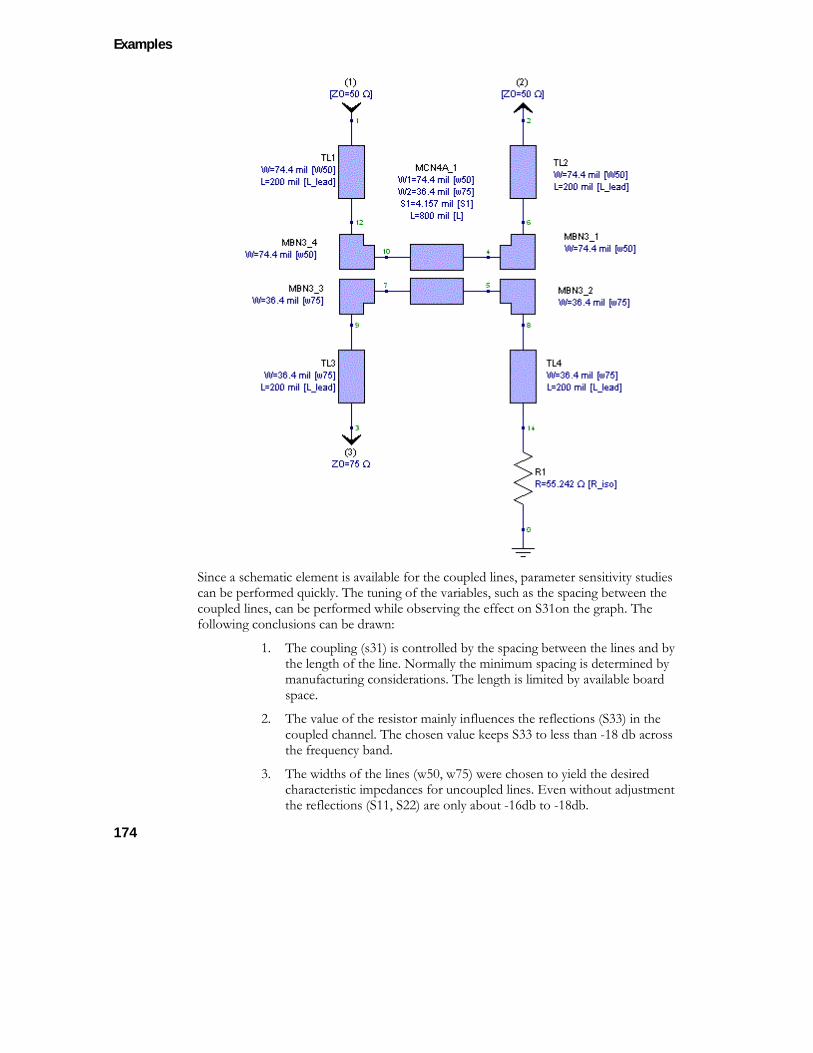
Examples
174
Since a schematic element is available for the coupled lines, parameter sensitivity studies can be performed quickly. The tuning of the variables, such as the spacing between the coupled lines, can be performed while observing the effect on S31on the graph. The following conclusions can be drawn:
1. The coupling (s31) is controlled by the spacing between the lines and by the length of the line. Normally the minimum spacing is determined by manufacturing considerations. The length is limited by available board space.
2. The value of the resistor mainly influences the reflections (S33) in the coupled channel. The chosen value keeps S33 to less than -18 db across the frequency band.
3. The widths of the lines (w50, w75) were chosen to yield the desired characteristic impedances for uncoupled lines. Even without adjustment the reflections (S11, S22) are only about -16db to -18db.
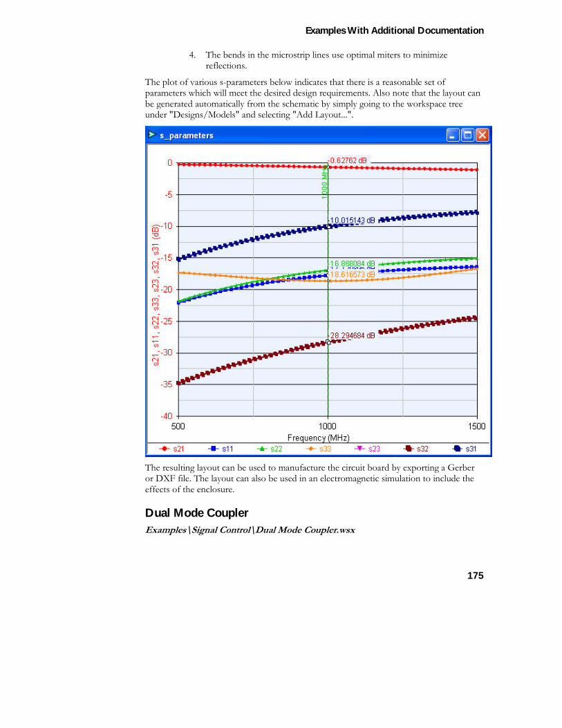
Examples With Additional Documentation
175
4. The bends in the microstrip lines use optimal miters to minimize reflections.
The plot of various s-parameters below indicates that there is a reasonable set of parameters which will meet the desired design requirements. Also note that the layout can be generated automatically from the schematic by simply going to the workspace tree under "Designs/Models" and selecting "Add Layout...".
The resulting layout can be used to manufacture the circuit board by exporting a Gerber or DXF file. The layout can also be used in an electromagnetic simulation to include the effects of the enclosure.
Dual Mode Coupler Examples\Signal Control\Dual Mode Coupler.wsx
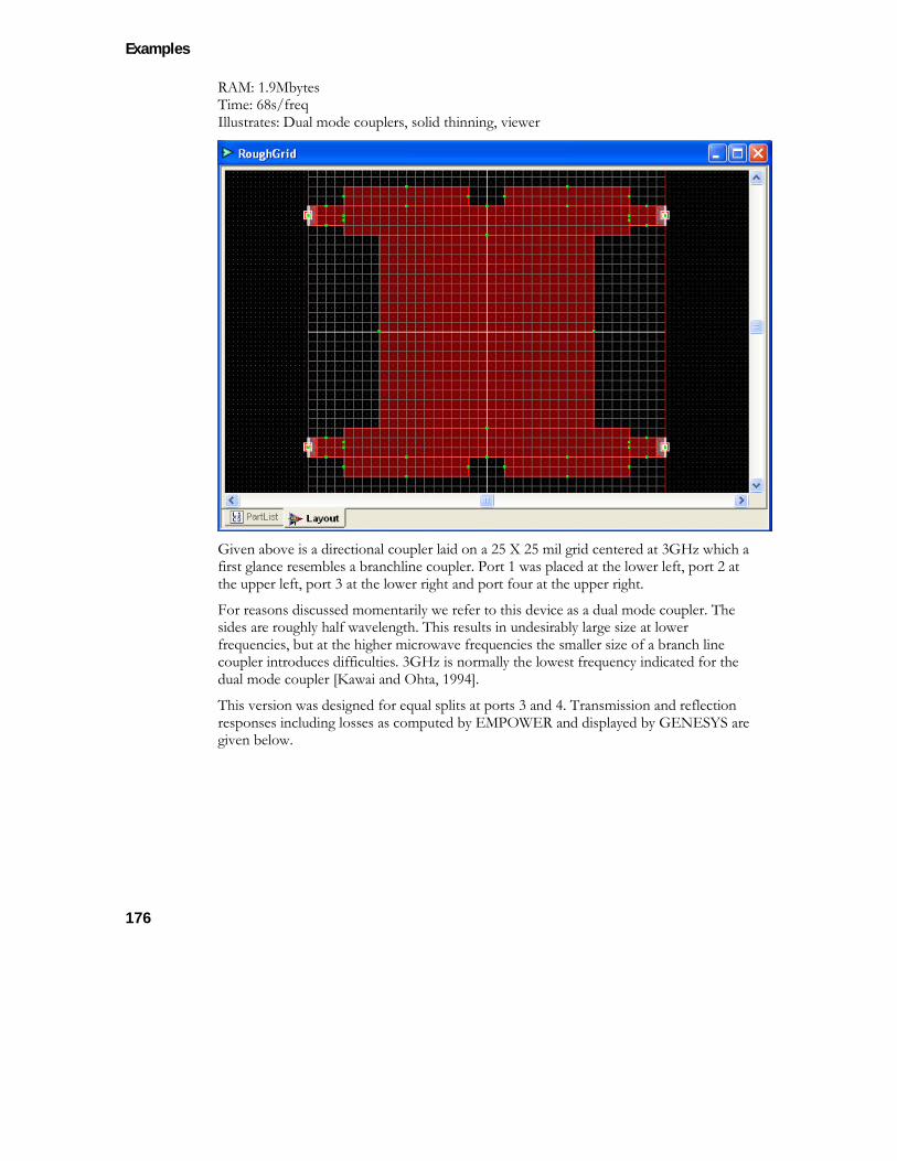
Examples
176
RAM: 1.9Mbytes Time: 68s/freq Illustrates: Dual mode couplers, solid thinning, viewer
Given above is a directional coupler laid on a 25 X 25 mil grid centered at 3GHz which a first glance resembles a branchline coupler. Port 1 was placed at the lower left, port 2 at the upper left, port 3 at the lower right and port four at the upper right.
For reasons discussed momentarily we refer to this device as a dual mode coupler. The sides are roughly half wavelength. This results in undesirably large size at lower frequencies, but at the higher microwave frequencies the smaller size of a branch line coupler introduces difficulties. 3GHz is normally the lowest frequency indicated for the dual mode coupler [Kawai and Ohta, 1994].
This version was designed for equal splits at ports 3 and 4. Transmission and reflection responses including losses as computed by EMPOWER and displayed by GENESYS are given below.
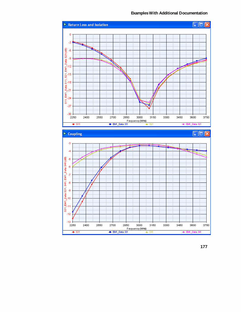
Examples With Additional Documentation
177
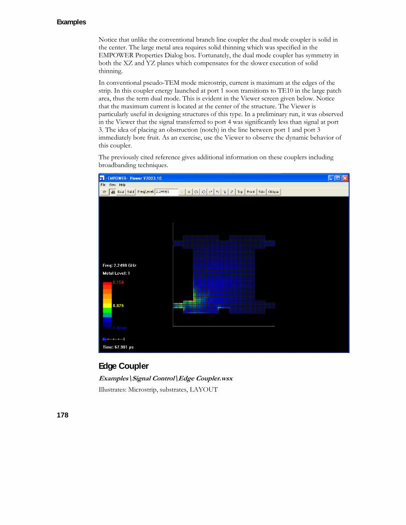
Examples
178
Notice that unlike the conventional branch line coupler the dual mode coupler is solid in the center. The large metal area requires solid thinning which was specified in the EMPOWER Properties Dialog box. Fortunately, the dual mode coupler has symmetry in both the XZ and YZ planes which compensates for the slower execution of solid thinning.
In conventional pseudo-TEM mode microstrip, current is maximum at the edges of the strip. In this coupler energy launched at port 1 soon transitions to TE10 in the large patch area, thus the term dual mode. This is evident in the Viewer screen given below. Notice that the maximum current is located at the center of the structure. The Viewer is particularly useful in designing structures of this type. In a preliminary run, it was observed in the Viewer that the signal transferred to port 4 was significantly less than signal at port 3. The idea of placing an obstruction (notch) in the line between port 1 and port 3 immediately bore fruit. As an exercise, use the Viewer to observe the dynamic behavior of this coupler.
The previously cited reference gives additional information on these couplers including broadbanding techniques.
Edge Coupler Examples\Signal Control\Edge Coupler.wsx Illustrates: Microstrip, substrates, LAYOUT
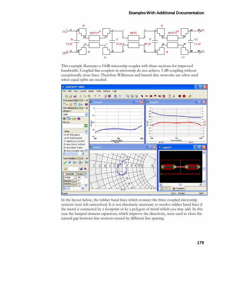
Examples With Additional Documentation
179
This example illustrates a 10dB microstrip coupler with three sections for improved bandwidth. Coupled-line couplers in microstrip do not achieve 3 dB coupling without exceptionally close lines. Therefore Wilkinson and branch-line networks are often used when equal splits are needed.
In the layout below, the rubber band lines which connect the three coupled microstrip sections were left unresolved. It is not absolutely neccesary to resolve rubber band lines if the metal is connected by a footprint or by a polygon of metal which you may add. In this case the lumped element capacitors, which improve the directivity, were used to close the natural gap between line sections caused by different line spacing.
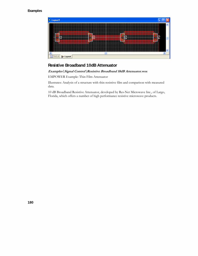
Examples
180
Resistive Broadband 10dB Attenuator Examples\Signal Control\Resistive Broadband 10dB Attenuator.wsx EMPOWER Example: Thin Film Attenuator
Illustrates: Analysis of a structure with thin resistive film and comparison with measured data.
10 dB Broadband Resistive Attenuator, developed by Res-Net Microwave Inc., of Largo, Florida, which offers a number of high performance resistive microwave products.
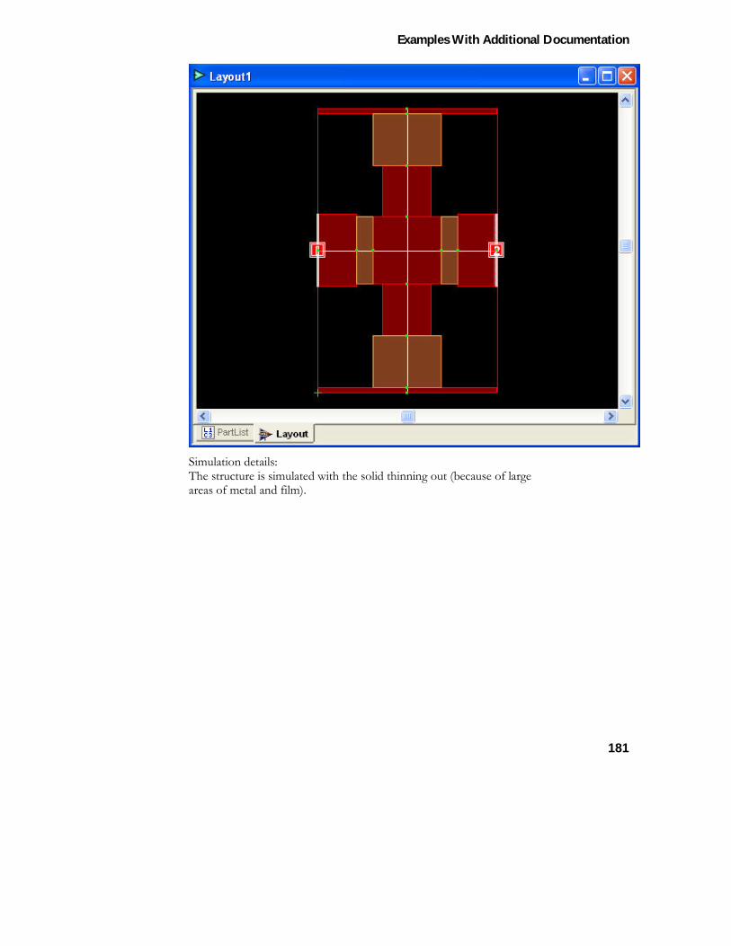
Examples With Additional Documentation
181
Simulation details: The structure is simulated with the solid thinning out (because of large areas of metal and film).
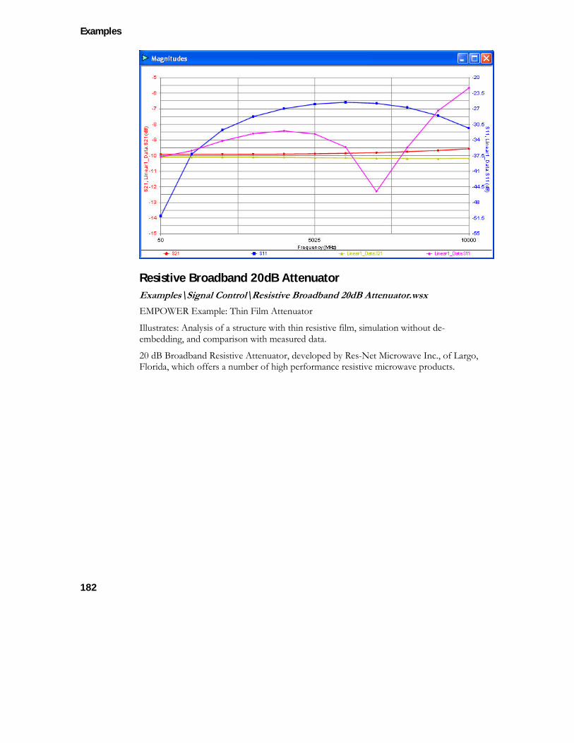
Examples
182
Resistive Broadband 20dB Attenuator Examples\Signal Control\Resistive Broadband 20dB Attenuator.wsx EMPOWER Example: Thin Film Attenuator
Illustrates: Analysis of a structure with thin resistive film, simulation without de-embedding, and comparison with measured data.
20 dB Broadband Resistive Attenuator, developed by Res-Net Microwave Inc., of Largo, Florida, which offers a number of high performance resistive microwave products.
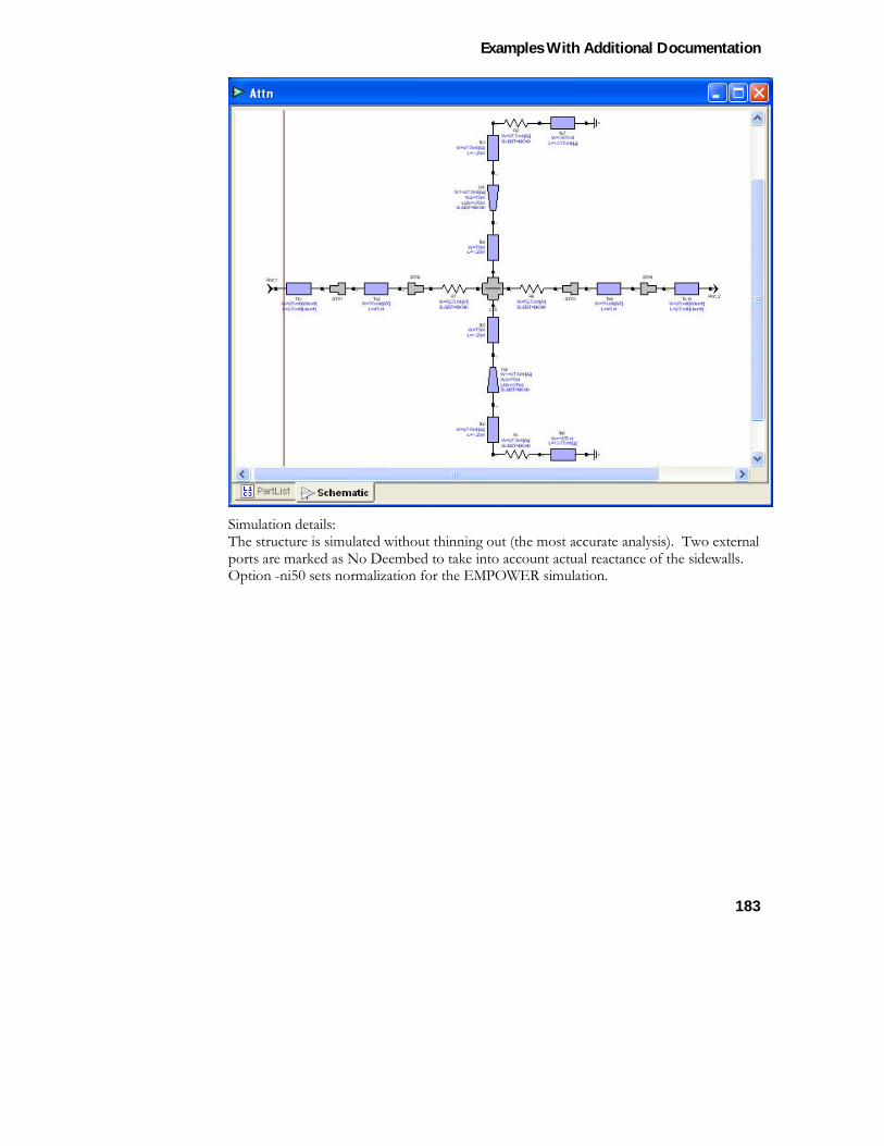
Examples With Additional Documentation
183
Simulation details: The structure is simulated without thinning out (the most accurate analysis). Two external ports are marked as No Deembed to take into account actual reactance of the sidewalls. Option -ni50 sets normalization for the EMPOWER simulation.
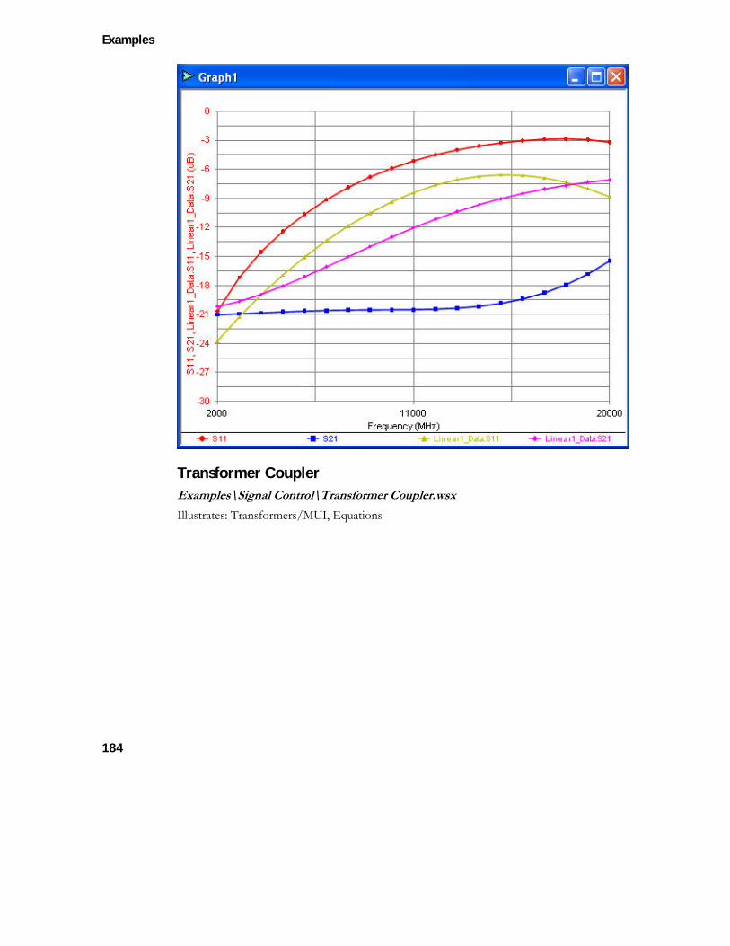
Examples
184
Transformer Coupler Examples\Signal Control\Transformer Coupler.wsx Illustrates: Transformers/MUI, Equations
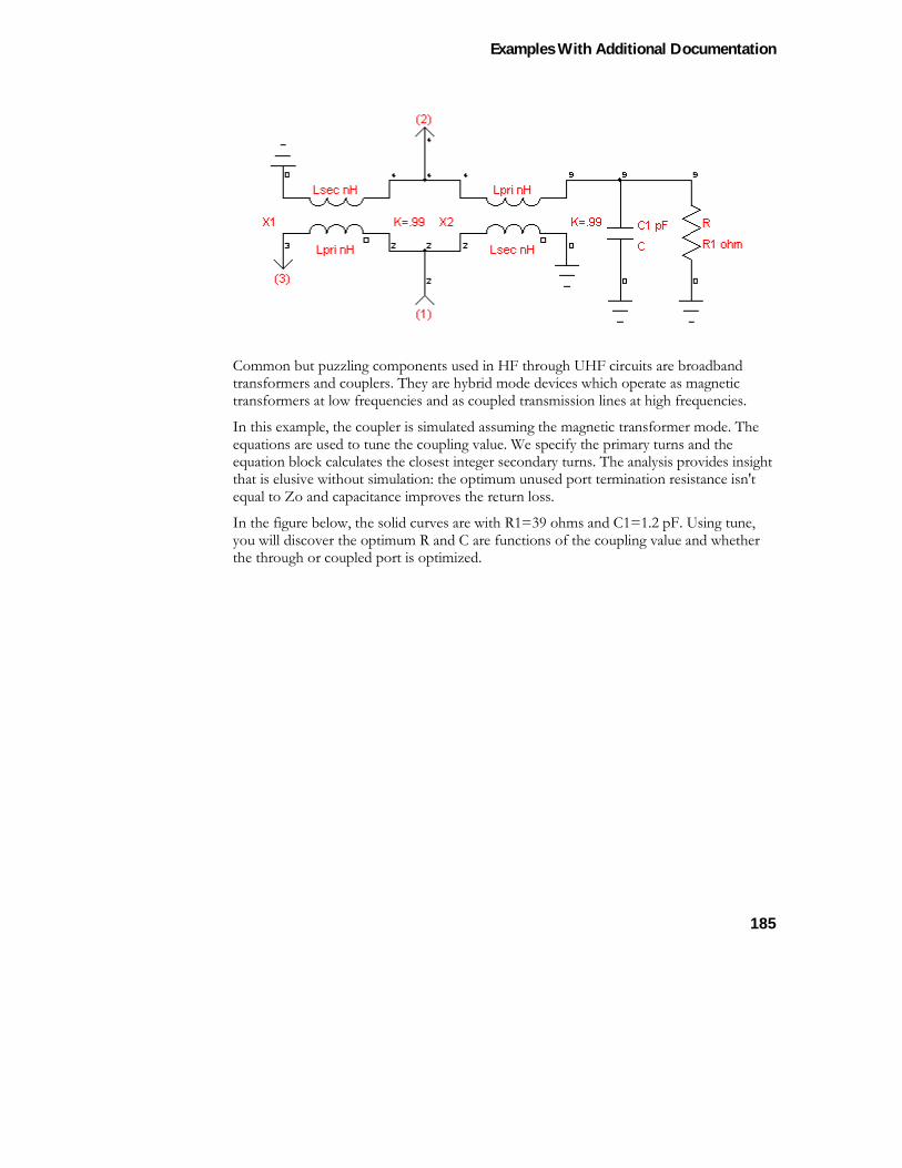
Examples With Additional Documentation
185
Common but puzzling components used in HF through UHF circuits are broadband transformers and couplers. They are hybrid mode devices which operate as magnetic transformers at low frequencies and as coupled transmission lines at high frequencies.
In this example, the coupler is simulated assuming the magnetic transformer mode. The equations are used to tune the coupling value. We specify the primary turns and the equation block calculates the closest integer secondary turns. The analysis provides insight that is elusive without simulation: the optimum unused port termination resistance isn't equal to Zo and capacitance improves the return loss.
In the figure below, the solid curves are with R1=39 ohms and C1=1.2 pF. Using tune, you will discover the optimum R and C are functions of the coupling value and whether the through or coupled port is optimized.
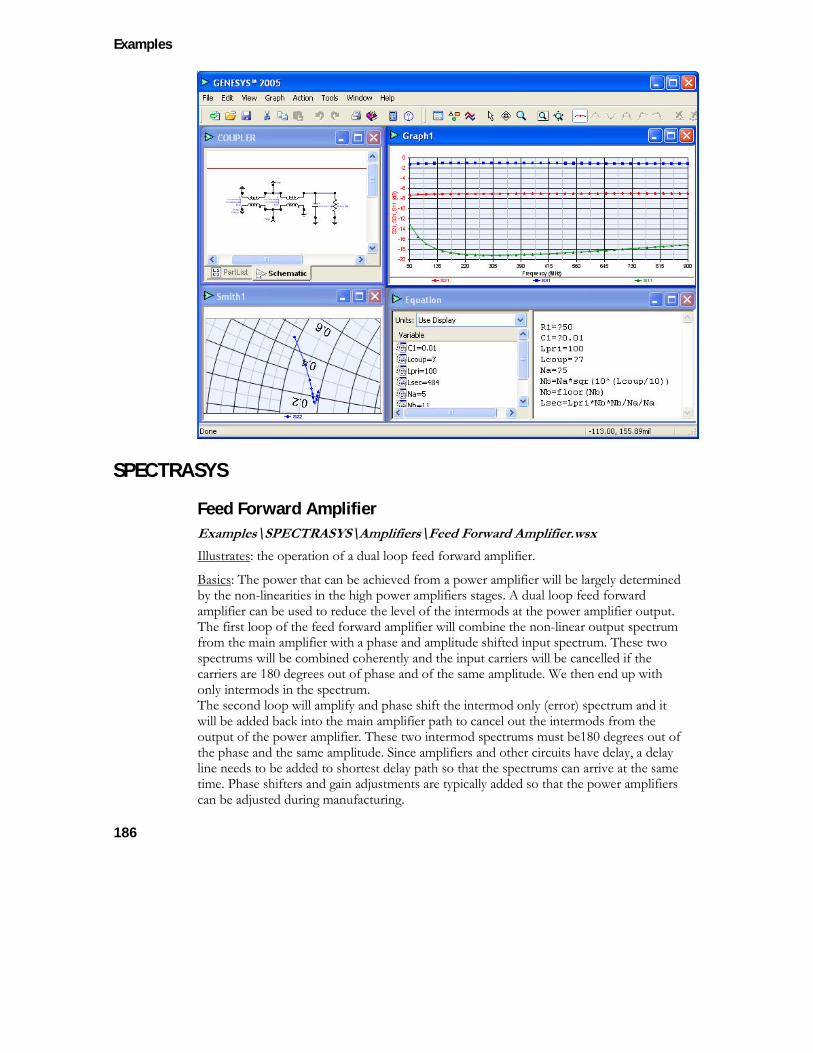
Examples
186
SPECTRASYS
Feed Forward Amplifier Examples\SPECTRASYS\Amplifiers\Feed Forward Amplifier.wsx Illustrates: the operation of a dual loop feed forward amplifier.
Basics: The power that can be achieved from a power amplifier will be largely determined by the non-linearities in the high power amplifiers stages. A dual loop feed forward amplifier can be used to reduce the level of the intermods at the power amplifier output. The first loop of the feed forward amplifier will combine the non-linear output spectrum from the main amplifier with a phase and amplitude shifted input spectrum. These two spectrums will be combined coherently and the input carriers will be cancelled if the carriers are 180 degrees out of phase and of the same amplitude. We then end up with only intermods in the spectrum. The second loop will amplify and phase shift the intermod only (error) spectrum and it will be added back into the main amplifier path to cancel out the intermods from the output of the power amplifier. These two intermod spectrums must be180 degrees out of the phase and the same amplitude. Since amplifiers and other circuits have delay, a delay line needs to be added to shortest delay path so that the spectrums can arrive at the same time. Phase shifters and gain adjustments are typically added so that the power amplifiers can be adjusted during manufacturing.
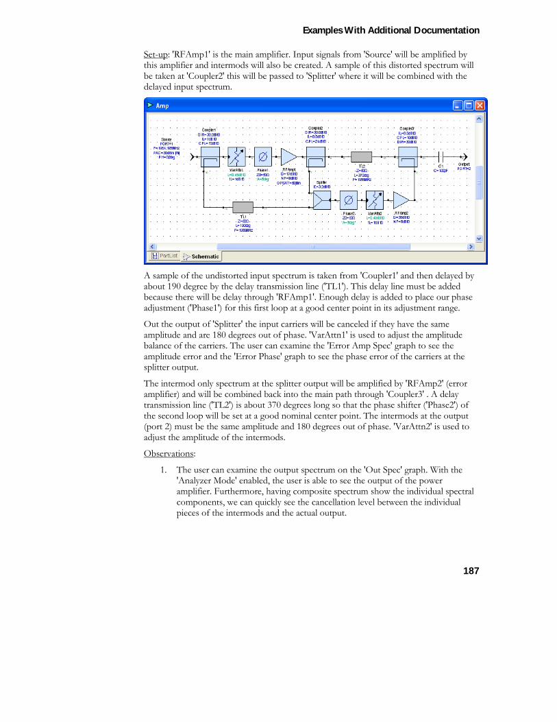
Examples With Additional Documentation
187
Set-up: 'RFAmp1' is the main amplifier. Input signals from 'Source' will be amplified by this amplifier and intermods will also be created. A sample of this distorted spectrum will be taken at 'Coupler2' this will be passed to 'Splitter' where it will be combined with the delayed input spectrum.
A sample of the undistorted input spectrum is taken from 'Coupler1' and then delayed by about 190 degree by the delay transmission line ('TL1'). This delay line must be added because there will be delay through 'RFAmp1'. Enough delay is added to place our phase adjustment ('Phase1') for this first loop at a good center point in its adjustment range.
Out the output of 'Splitter' the input carriers will be canceled if they have the same amplitude and are 180 degrees out of phase. 'VarAttn1' is used to adjust the amplitude balance of the carriers. The user can examine the 'Error Amp Spec' graph to see the amplitude error and the 'Error Phase' graph to see the phase error of the carriers at the splitter output.
The intermod only spectrum at the splitter output will be amplified by 'RFAmp2' (error amplifier) and will be combined back into the main path through 'Coupler3' . A delay transmission line ('TL2') is about 370 degrees long so that the phase shifter ('Phase2') of the second loop will be set at a good nominal center point. The intermods at the output (port 2) must be the same amplitude and 180 degrees out of phase. 'VarAttn2' is used to adjust the amplitude of the intermods.
Observations:
1. The user can examine the output spectrum on the 'Out Spec' graph. With the 'Analyzer Mode' enabled, the user is able to see the output of the power amplifier. Furthermore, having composite spectrum show the individual spectral components, we can quickly see the cancellation level between the individual pieces of the intermods and the actual output.
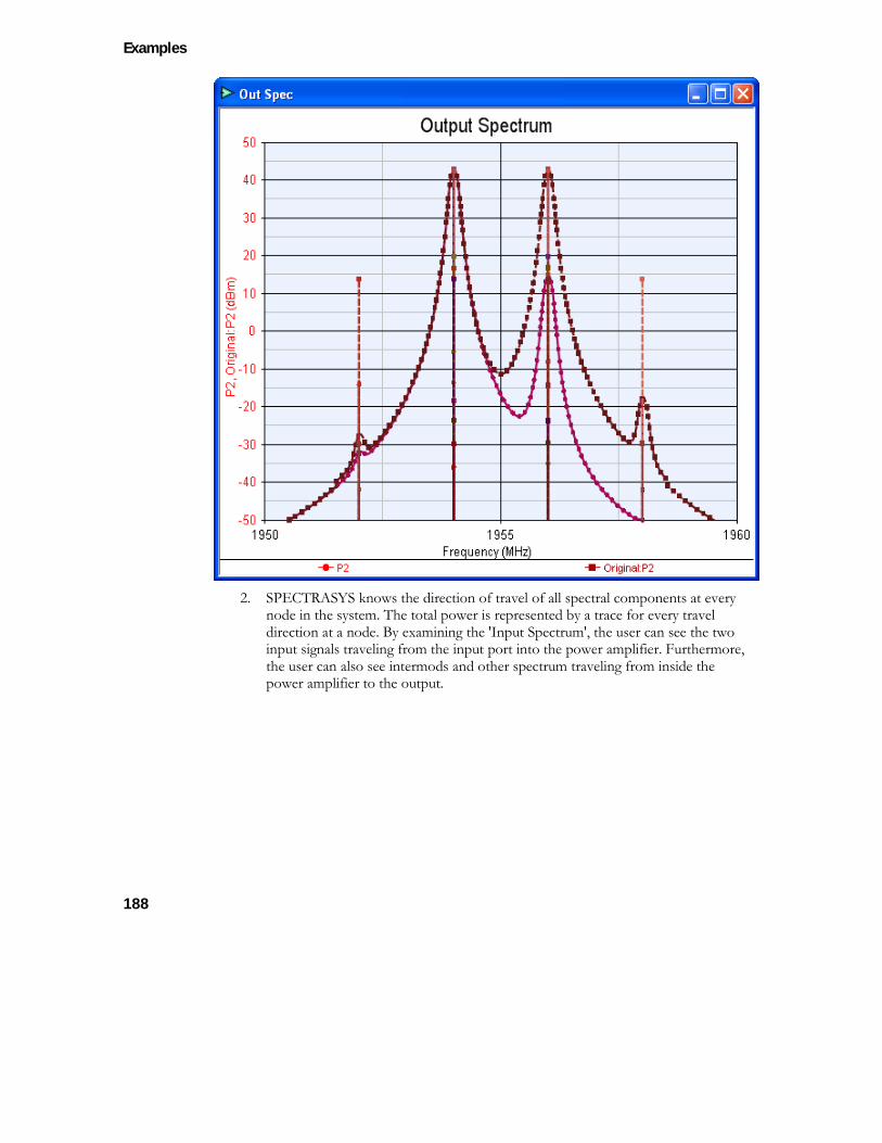
Examples
188
2. SPECTRASYS knows the direction of travel of all spectral components at every
node in the system. The total power is represented by a trace for every travel direction at a node. By examining the 'Input Spectrum', the user can see the two input signals traveling from the input port into the power amplifier. Furthermore, the user can also see intermods and other spectrum traveling from inside the power amplifier to the output.
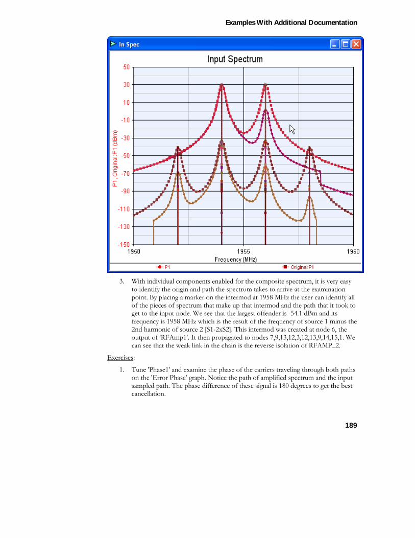
Examples With Additional Documentation
189
3. With individual components enabled for the composite spectrum, it is very easy
to identify the origin and path the spectrum takes to arrive at the examination point. By placing a marker on the intermod at 1958 MHz the user can identify all of the pieces of spectrum that make up that intermod and the path that it took to get to the input node. We see that the largest offender is -54.1 dBm and its frequency is 1958 MHz which is the result of the frequency of source 1 minus the 2nd harmonic of source 2 [S1-2xS2]. This intermod was created at node 6, the output of 'RFAmp1'. It then propagated to nodes 7,9,13,12,3,12,13,9,14,15,1. We can see that the weak link in the chain is the reverse isolation of RFAMP_2.
Exercises:
1. Tune 'Phase1' and examine the phase of the carriers traveling through both paths on the 'Error Phase' graph. Notice the path of amplified spectrum and the input sampled path. The phase difference of these signal is 180 degrees to get the best cancellation.

Examples
190
2. Tune 'Phase2' and examine the phase of the intermods traveling through both paths on the 'Out Phase' graph. Notice path of main spectrum and the input sampled path. Again, the phase difference of these signal is 180 degrees to get the best cancellation.
3. Tune 'VarAttn1' and 'VarAttn2' and watch the respective amplitude balance for the carriers and intermods with the 'Error Spec' and 'Out Spec' graphs.
4. Tune the reverse isolation of 'RFAmp2' and observe the intermod spectrum on the input ('Input Spectrum' graph) and notice that the improvement will change linearly with this isolation until the next dominant component is reached.
Quad Hybrid Matrix Amp Examples\SPECTRASYS\Amplifiers\Quad Hybrid Matrix Amp.wsx Abstract: The hybrid matrix amplifier is a popular power amplifier configuration that incorporates redundancy. With the traditional design of using a single power amplifier for every transmitter the power amplifier becomes a single point of failure. If the amplifier dies, then so does the carrier and all of the transmitted information. The hybrid matrix amplifier will still provide output power (albeit a lower output power ... due to the loss of one amplifier) for all input signals. Furthermore, the reliability of power amplifiers is typically lower than the transmitter, so the likelihood of losing a carrier can be very high.
Background: 90 Degree hybrid couplers are used at the input to shift each input signal (IN and ISO) by 90 degrees (ISO to 0 is a 90 degree shift and ISO to -90 is a 0 degree shift). These hybrid couplers are also used on the output to combine the amplified signals back together. Because of the phasing, carriers will either add or cancel at the output leaving a dedicated output for each carrier.
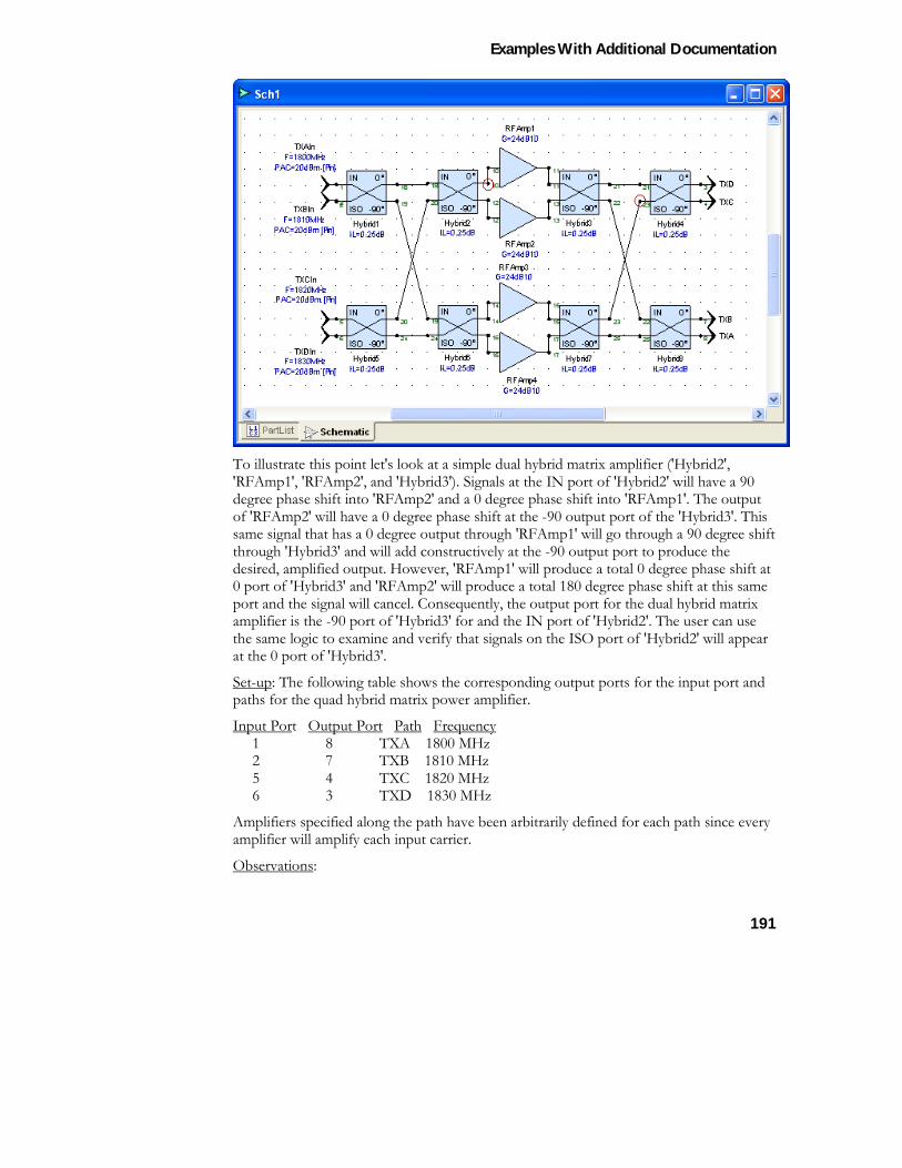
Examples With Additional Documentation
191
To illustrate this point let's look at a simple dual hybrid matrix amplifier ('Hybrid2', 'RFAmp1', 'RFAmp2', and 'Hybrid3'). Signals at the IN port of 'Hybrid2' will have a 90 degree phase shift into 'RFAmp2' and a 0 degree phase shift into 'RFAmp1'. The output of 'RFAmp2' will have a 0 degree phase shift at the -90 output port of the 'Hybrid3'. This same signal that has a 0 degree output through 'RFAmp1' will go through a 90 degree shift through 'Hybrid3' and will add constructively at the -90 output port to produce the desired, amplified output. However, 'RFAmp1' will produce a total 0 degree phase shift at 0 port of 'Hybrid3' and 'RFAmp2' will produce a total 180 degree phase shift at this same port and the signal will cancel. Consequently, the output port for the dual hybrid matrix amplifier is the -90 port of 'Hybrid3' for and the IN port of 'Hybrid2'. The user can use the same logic to examine and verify that signals on the ISO port of 'Hybrid2' will appear at the 0 port of 'Hybrid3'.
Set-up: The following table shows the corresponding output ports for the input port and paths for the quad hybrid matrix power amplifier.
Input Port Output Port Path Frequency 1 8 TXA 1800 MHz 2 7 TXB 1810 MHz 5 4 TXC 1820 MHz 6 3 TXD 1830 MHz
Amplifiers specified along the path have been arbitrarily defined for each path since every amplifier will amplify each input carrier.
Observations:
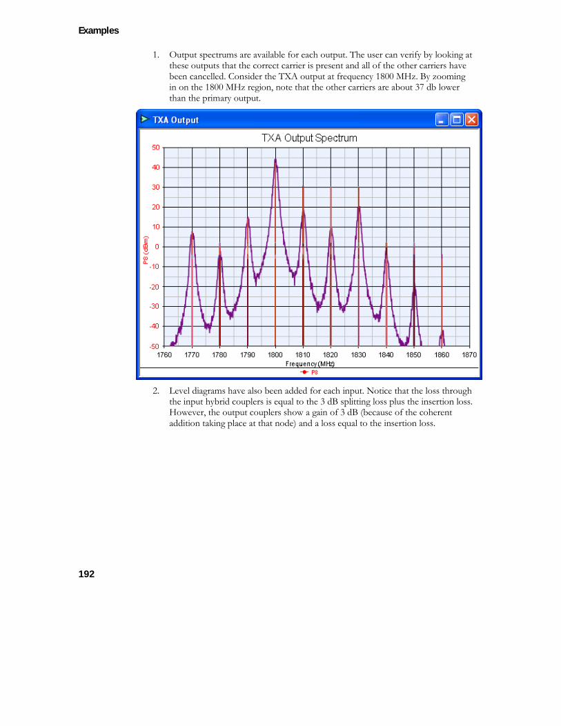
Examples
192
1. Output spectrums are available for each output. The user can verify by looking at these outputs that the correct carrier is present and all of the other carriers have been cancelled. Consider the TXA output at frequency 1800 MHz. By zooming in on the 1800 MHz region, note that the other carriers are about 37 db lower than the primary output.
2. Level diagrams have also been added for each input. Notice that the loss through
the input hybrid couplers is equal to the 3 dB splitting loss plus the insertion loss. However, the output couplers show a gain of 3 dB (because of the coherent addition taking place at that node) and a loss equal to the insertion loss.
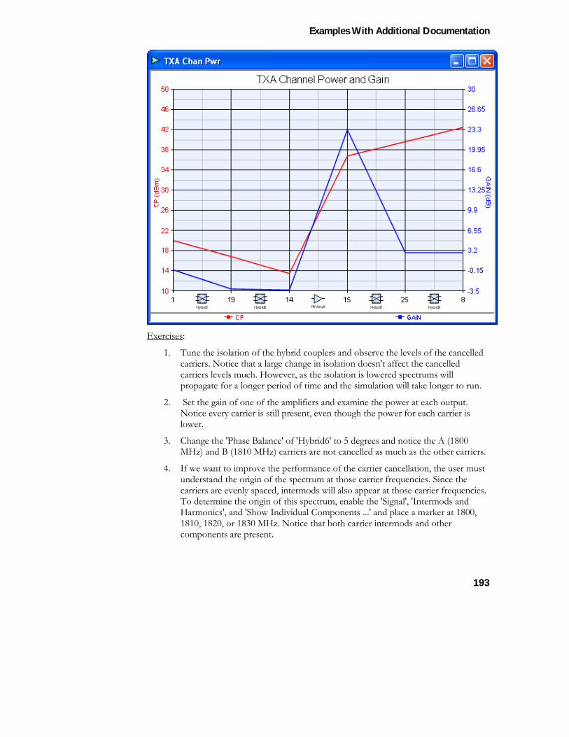
Examples With Additional Documentation
193
Exercises:
1. Tune the isolation of the hybrid couplers and observe the levels of the cancelled carriers. Notice that a large change in isolation doesn't affect the cancelled carriers levels much. However, as the isolation is lowered spectrums will propagate for a longer period of time and the simulation will take longer to run.
2. Set the gain of one of the amplifiers and examine the power at each output. Notice every carrier is still present, even though the power for each carrier is lower.
3. Change the 'Phase Balance' of 'Hybrid6' to 5 degrees and notice the A (1800 MHz) and B (1810 MHz) carriers are not cancelled as much as the other carriers.
4. If we want to improve the performance of the carrier cancellation, the user must understand the origin of the spectrum at those carrier frequencies. Since the carriers are evenly spaced, intermods will also appear at those carrier frequencies. To determine the origin of this spectrum, enable the 'Signal', 'Intermods and Harmonics', and 'Show Individual Components ...' and place a marker at 1800, 1810, 1820, or 1830 MHz. Notice that both carrier intermods and other components are present.
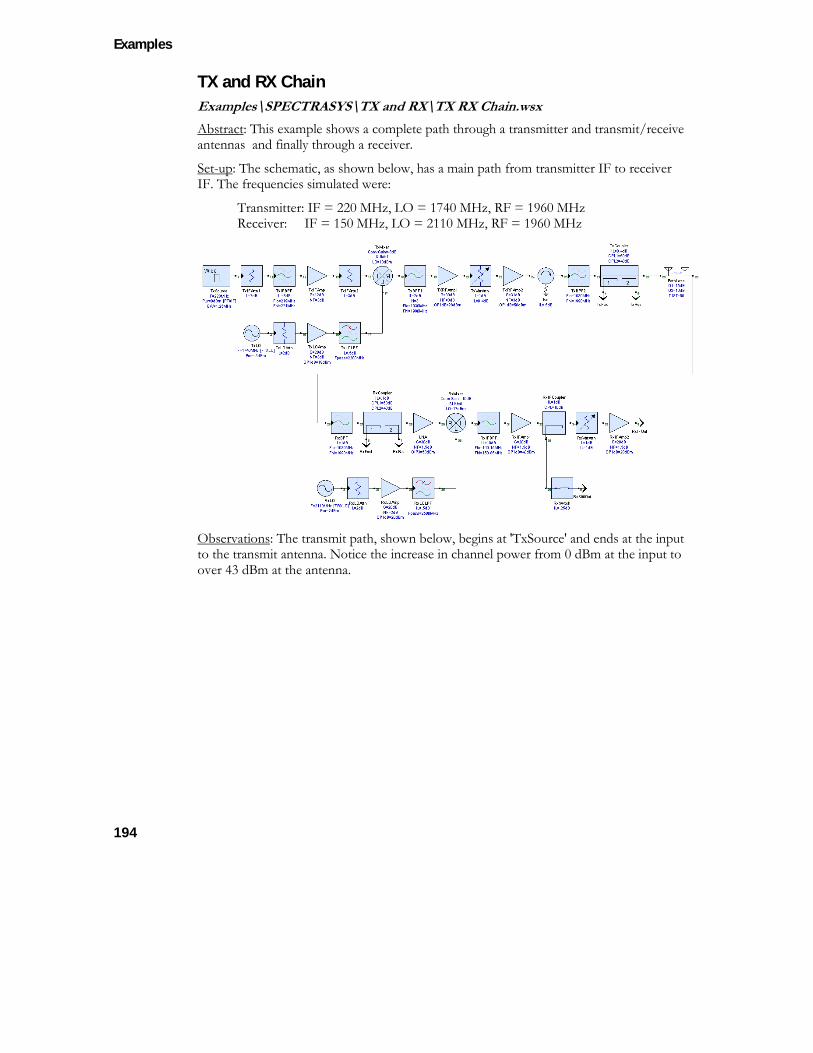
Examples
194
TX and RX Chain Examples\SPECTRASYS\TX and RX\TX RX Chain.wsx Abstract: This example shows a complete path through a transmitter and transmit/receive antennas and finally through a receiver.
Set-up: The schematic, as shown below, has a main path from transmitter IF to receiver IF. The frequencies simulated were:
Transmitter: IF = 220 MHz, LO = 1740 MHz, RF = 1960 MHz Receiver: IF = 150 MHz, LO = 2110 MHz, RF = 1960 MHz
Observations: The transmit path, shown below, begins at 'TxSource' and ends at the input to the transmit antenna. Notice the increase in channel power from 0 dBm at the input to over 43 dBm at the antenna.
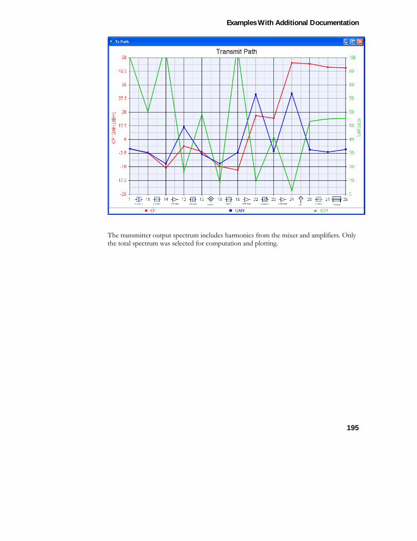
Examples With Additional Documentation
195
The transmitter output spectrum includes harmonics from the mixer and amplifiers. Only the total spectrum was selected for computation and plotting.
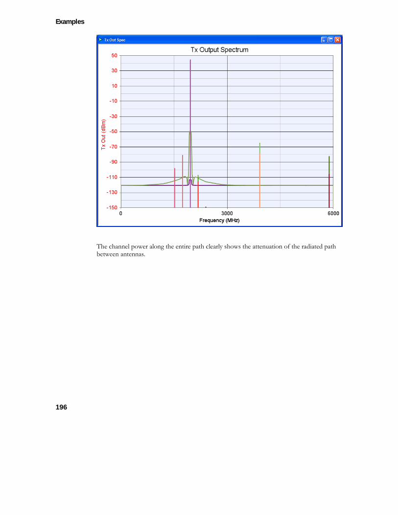
Examples
196
The channel power along the entire path clearly shows the attenuation of the radiated path between antennas.
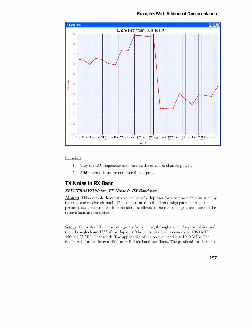
Examples With Additional Documentation
197
Exercises:
1. Vary the LO frequencies and observe the effect on channel power.
2. Add intermods and re-compute the outputs.
TX Noise in RX Band SPECTRASYS\Noise\TX Noise in RX Band.wsx Abstract: This example demonstrates the use of a duplexer for a common antenna used by transmit and receive channels. The issues related to the filter design parameters and performance are examined. In particular, the effects of the transmit signal and noise in the receive band are simulated.
Set-up: The path of the transmit signal is from 'TxIn', through the 'TxAmp' amplifier, and then through channel 'A' of the duplexer. The transmit signal is centered at 1960 MHz with a 1.25 MHz bandwidth. The upper edge of the receive band is at 1910 MHz. The duplexer is formed by two fifth order Elliptic bandpass filters. The passband for channels
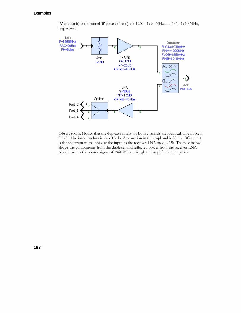
Examples
198
'A' (transmit) and channel 'B' (receive band) are 1930 - 1990 MHz and 1850-1910 MHz, respectively.
Observations: Notice that the duplexer filters for both channels are identical. The ripple is 0.5 db. The insertion loss is also 0.5 db. Attenuation in the stopband is 80 db. Of interest is the spectrum of the noise at the input to the receiver LNA (node # 9). The plot below shows the components from the duplexer and reflected power from the receiver LNA. Also shown is the source signal of 1960 MHz through the amplifier and duplexer.
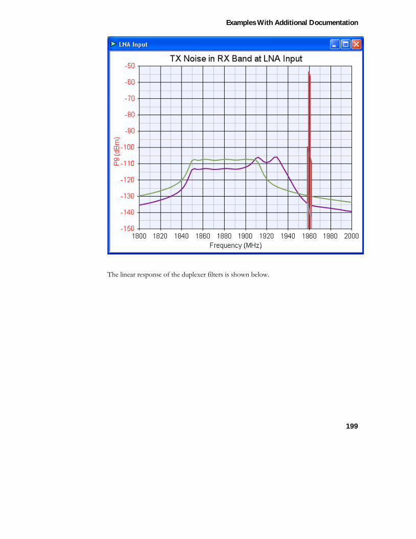
Examples With Additional Documentation
199
The linear response of the duplexer filters is shown below.
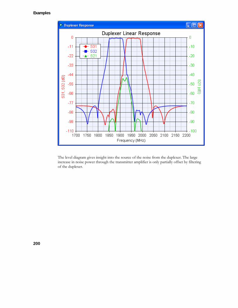
Examples
200
The level diagram gives insight into the source of the noise from the duplexer. The large increase in noise power through the transmitter amplifier is only partially offset by filtering of the duplexer.
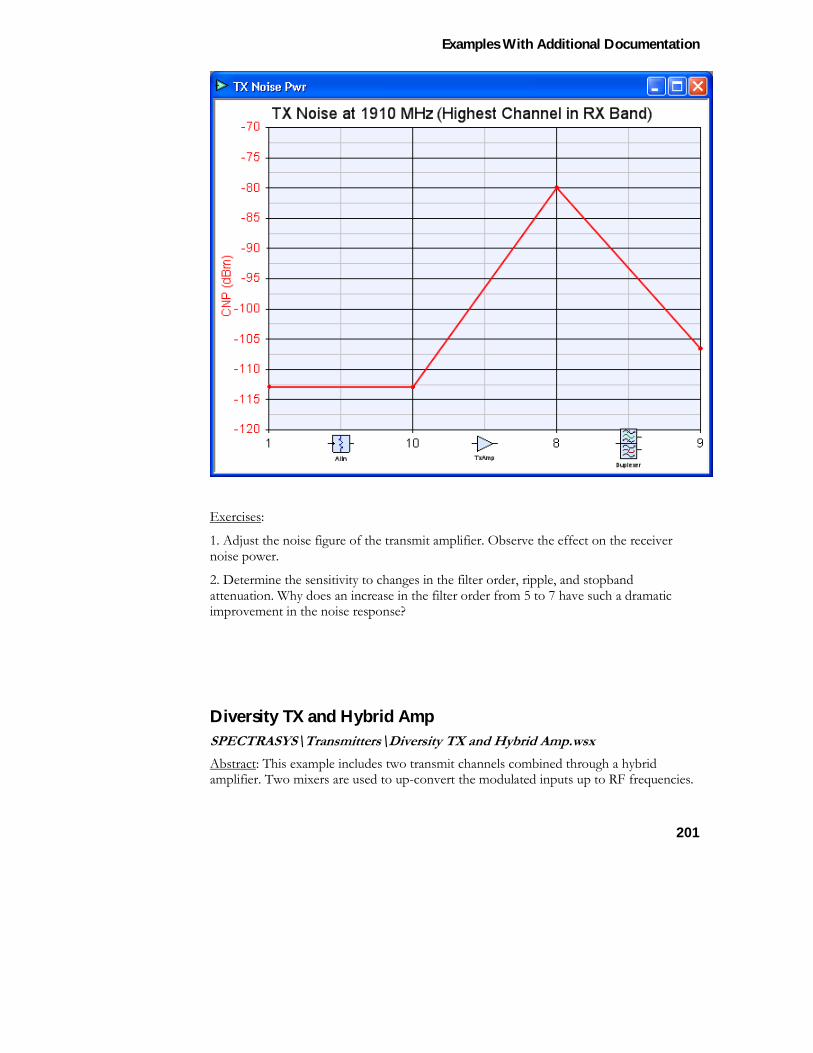
Examples With Additional Documentation
201
Exercises:
1. Adjust the noise figure of the transmit amplifier. Observe the effect on the receiver noise power.
2. Determine the sensitivity to changes in the filter order, ripple, and stopband attenuation. Why does an increase in the filter order from 5 to 7 have such a dramatic improvement in the noise response?
Diversity TX and Hybrid Amp SPECTRASYS\Transmitters\Diversity TX and Hybrid Amp.wsx Abstract: This example includes two transmit channels combined through a hybrid amplifier. Two mixers are used to up-convert the modulated inputs up to RF frequencies.
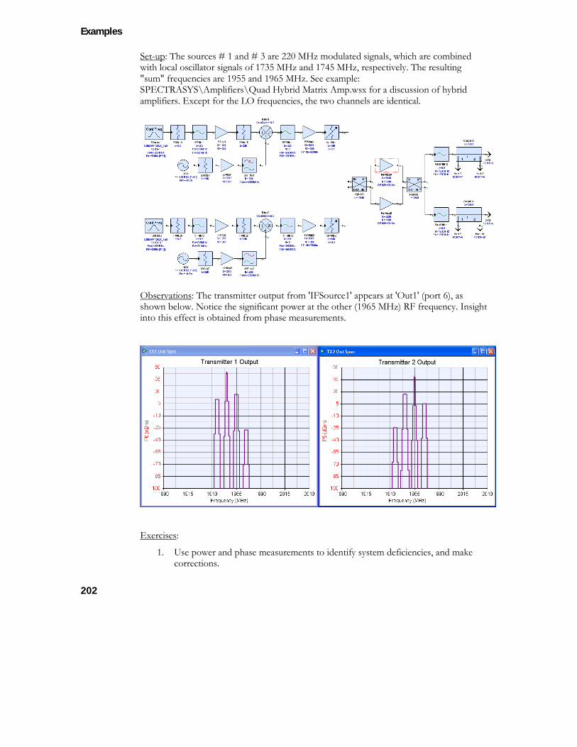
Examples
202
Set-up: The sources # 1 and # 3 are 220 MHz modulated signals, which are combined with local oscillator signals of 1735 MHz and 1745 MHz, respectively. The resulting "sum" frequencies are 1955 and 1965 MHz. See example: SPECTRASYS\Amplifiers\Quad Hybrid Matrix Amp.wsx for a discussion of hybrid amplifiers. Except for the LO frequencies, the two channels are identical.
Observations: The transmitter output from 'IFSource1' appears at 'Out1' (port 6), as shown below. Notice the significant power at the other (1965 MHz) RF frequency. Insight into this effect is obtained from phase measurements.
Exercises:
1. Use power and phase measurements to identify system deficiencies, and make corrections.
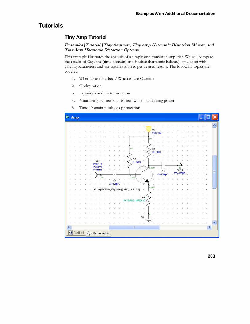
Examples With Additional Documentation
203
Tutorials
Tiny Amp Tutorial Examples\Tutorial \Tiny Amp.wsx, Tiny Amp Harmonic Distortion IM.wsx, and Tiny Amp Harmonic Distortion Opt.wsx This example illustrates the analysis of a simple one-transistor amplifier. We will compare the results of Cayenne (time-domain) and Harbec (harmonic balance) simulation with varying parameters and use optimization to get desired results. The following topics are covered:
1. When to use Harbec / When to use Cayenne
2. Optimization
3. Equations and vector notation
4. Minimizing harmonic distortion while maintaining power
5. Time-Domain result of optimization
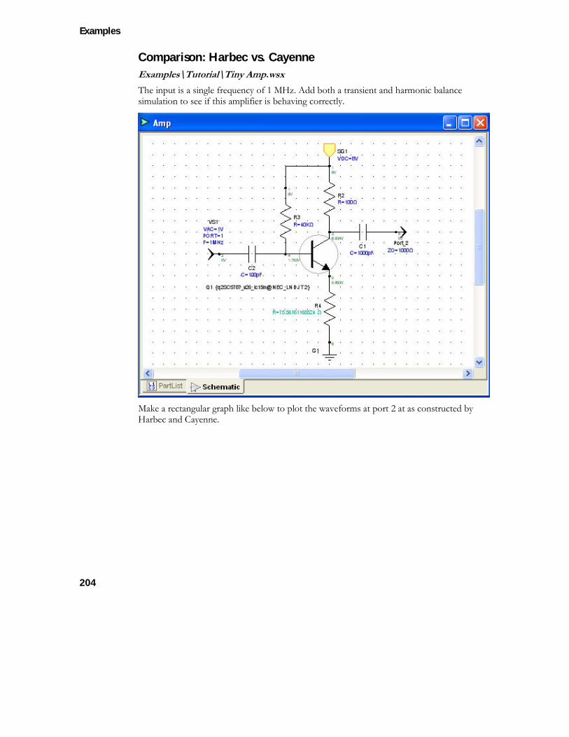
Examples
204
Comparison: Harbec vs. Cayenne Examples\Tutorial\Tiny Amp.wsx The input is a single frequency of 1 MHz. Add both a transient and harmonic balance simulation to see if this amplifier is behaving correctly.
Make a rectangular graph like below to plot the waveforms at port 2 at as constructed by Harbec and Cayenne.
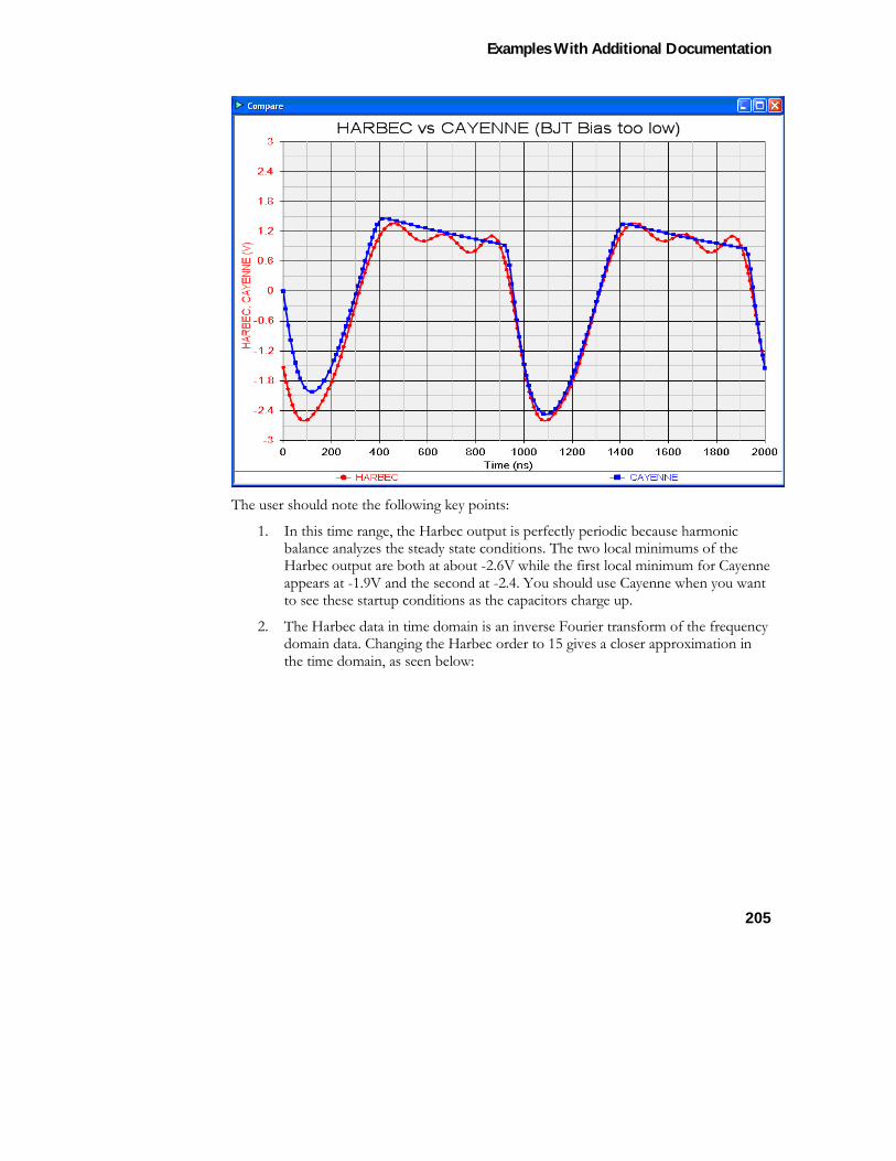
Examples With Additional Documentation
205
The user should note the following key points:
1. In this time range, the Harbec output is perfectly periodic because harmonic balance analyzes the steady state conditions. The two local minimums of the Harbec output are both at about -2.6V while the first local minimum for Cayenne appears at -1.9V and the second at -2.4. You should use Cayenne when you want to see these startup conditions as the capacitors charge up.
2. The Harbec data in time domain is an inverse Fourier transform of the frequency domain data. Changing the Harbec order to 15 gives a closer approximation in the time domain, as seen below:
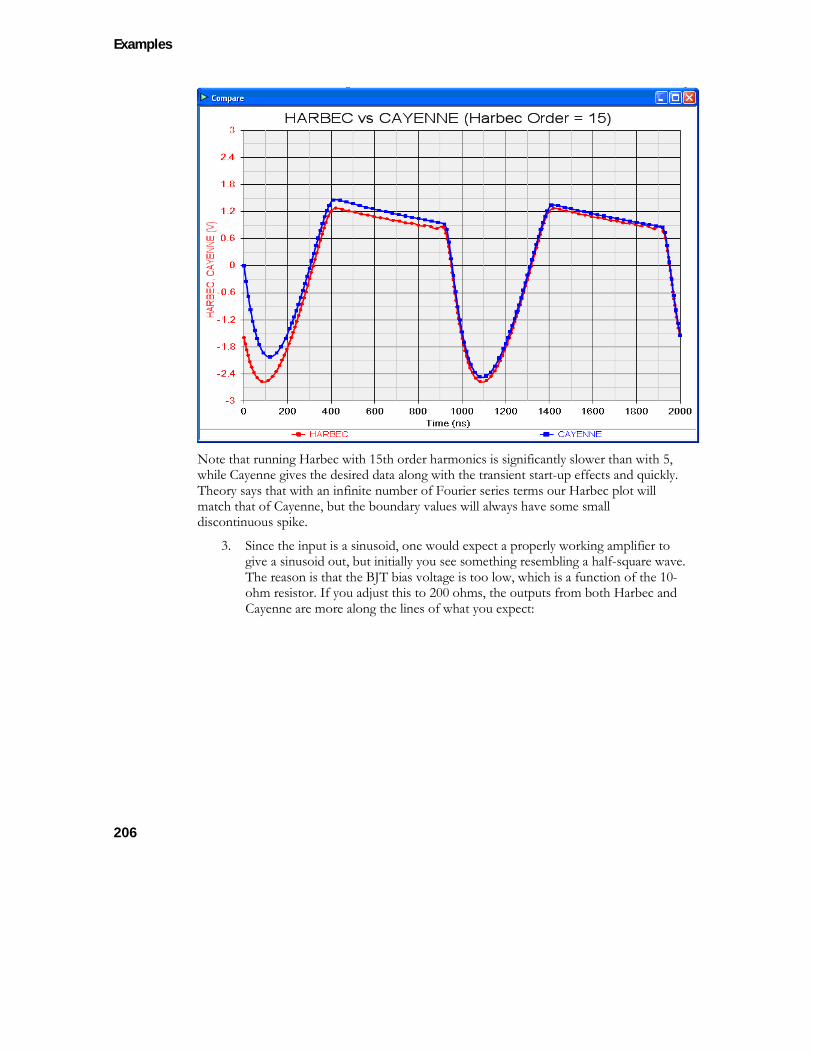
Examples
206
Note that running Harbec with 15th order harmonics is significantly slower than with 5, while Cayenne gives the desired data along with the transient start-up effects and quickly. Theory says that with an infinite number of Fourier series terms our Harbec plot will match that of Cayenne, but the boundary values will always have some small discontinuous spike.
3. Since the input is a sinusoid, one would expect a properly working amplifier to give a sinusoid out, but initially you see something resembling a half-square wave. The reason is that the BJT bias voltage is too low, which is a function of the 10-ohm resistor. If you adjust this to 200 ohms, the outputs from both Harbec and Cayenne are more along the lines of what you expect:
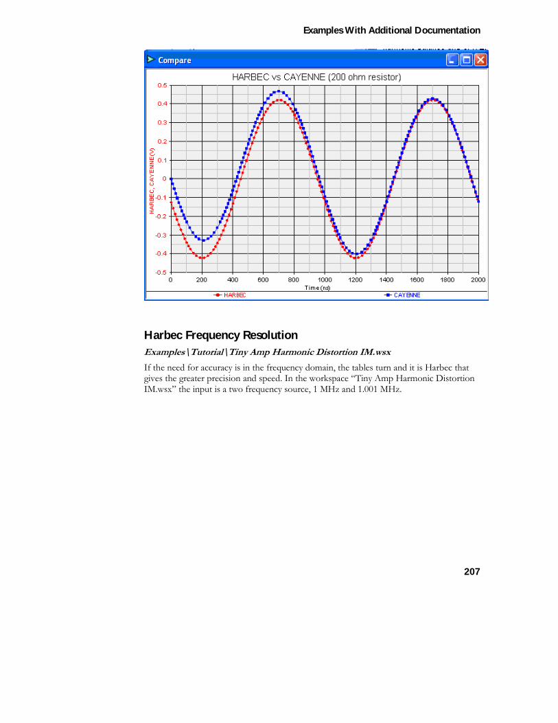
Examples With Additional Documentation
207
Harbec Frequency Resolution Examples\Tutorial\Tiny Amp Harmonic Distortion IM.wsx If the need for accuracy is in the frequency domain, the tables turn and it is Harbec that gives the greater precision and speed. In the workspace “Tiny Amp Harmonic Distortion IM.wsx” the input is a two frequency source, 1 MHz and 1.001 MHz.
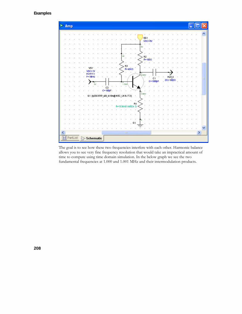
Examples
208
The goal is to see how these two frequencies interfere with each other. Harmonic balance allows you to see very fine frequency resolution that would take an impractical amount of time to compute using time domain simulation. In the below graph we see the two fundamental frequencies at 1.000 and 1.001 MHz and their intermodulation products.
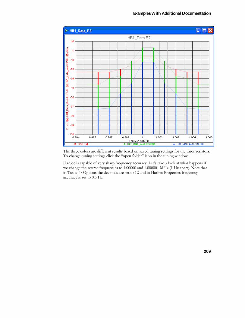
Examples With Additional Documentation
209
The three colors are different results based on saved tuning settings for the three resistors. To change tuning settings click the “open folder” icon in the tuning window.
Harbec is capable of very sharp frequency accuracy. Let’s take a look at what happens if we change the source frequencies to 1.00000 and 1.000001 MHz (1 Hz apart). Note that in Tools -> Options the decimals are set to 12 and in Harbec Properties frequency accuracy is set to 0.5 Hz.
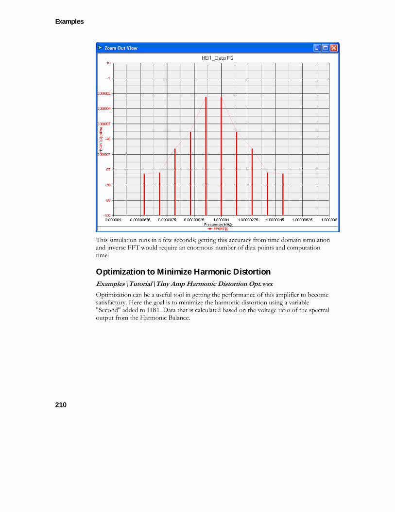
Examples
210
This simulation runs in a few seconds; getting this accuracy from time domain simulation and inverse FFT would require an enormous number of data points and computation time.
Optimization to Minimize Harmonic Distortion Examples\Tutorial\Tiny Amp Harmonic Distortion Opt.wsx Optimization can be a useful tool in getting the performance of this amplifier to become satisfactory. Here the goal is to minimize the harmonic distortion using a variable "Second" added to HB1_Data that is calculated based on the voltage ratio of the spectral output from the Harmonic Balance.
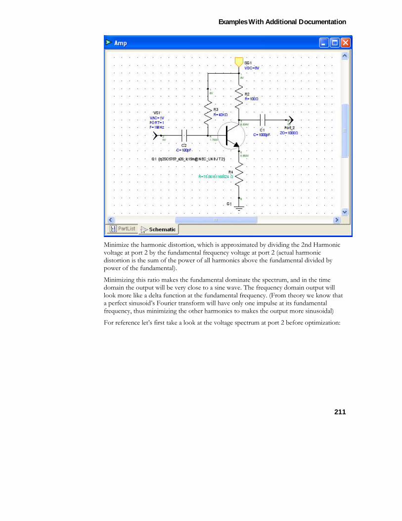
Examples With Additional Documentation
211
Minimize the harmonic distortion, which is approximated by dividing the 2nd Harmonic voltage at port 2 by the fundamental frequency voltage at port 2 (actual harmonic distortion is the sum of the power of all harmonics above the fundamental divided by power of the fundamental).
Minimizing this ratio makes the fundamental dominate the spectrum, and in the time domain the output will be very close to a sine wave. The frequency domain output will look more like a delta function at the fundamental frequency. (From theory we know that a perfect sinusoid’s Fourier transform will have only one impulse at its fundamental frequency, thus minimizing the other harmonics to makes the output more sinusoidal)
For reference let’s first take a look at the voltage spectrum at port 2 before optimization:
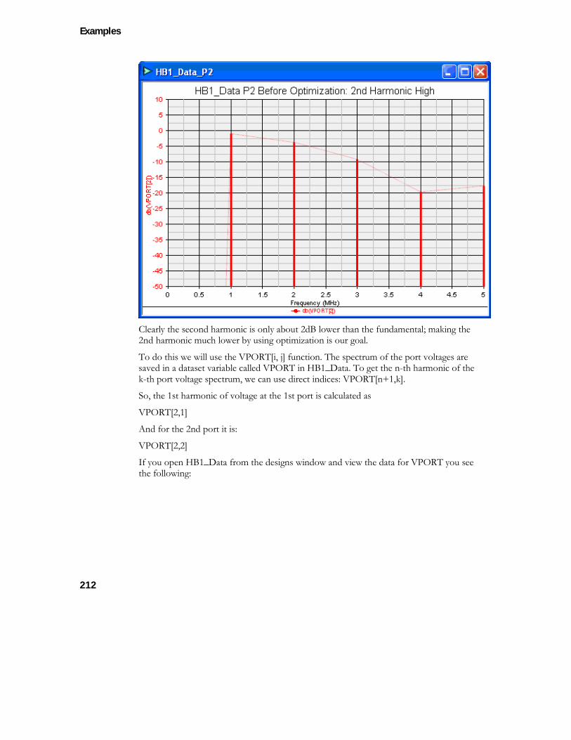
Examples
212
Clearly the second harmonic is only about 2dB lower than the fundamental; making the 2nd harmonic much lower by using optimization is our goal.
To do this we will use the VPORT[i, j] function. The spectrum of the port voltages are saved in a dataset variable called VPORT in HB1_Data. To get the n-th harmonic of the k-th port voltage spectrum, we can use direct indices: VPORT[n+1,k].
So, the 1st harmonic of voltage at the 1st port is calculated as
VPORT[2,1]
And for the 2nd port it is:
VPORT[2,2]
If you open HB1_Data from the designs window and view the data for VPORT you see the following:
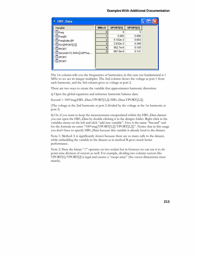
Examples With Additional Documentation
213
The 1st column tells you the frequencies of harmonics; in this case our fundamental is 1 MHz so we see its integer multiples. The 2nd column shows the voltage at port 1 from each harmonic, and the 3rd column gives us voltage at port 2.
There are two ways to create the variable that approximates harmonic distortion:
a] Open the global equations and reference harmonic balance data:
Second = 100*mag(HB1_Data.VPORT[3,2]/HB1_Data.VPORT[2,2])
(The voltage at the 2nd harmonic at port 2 divided by the voltage at the 1st harmonic at port 2)
b] Or, if you want to keep the measurements encapsulated within the HB1_Data dataset you can open the HB1_Data by double-clicking it in the designs folder. Right-click in the variables menu on the left and click “add new variable”. Give it the name “Second” and for the formula we enter “100*mag(VPORT[3,2]/VPORT[2,2])”. Notice that in this usage you don’t have to specify HB1_Data because this variable is already local to the dataset.
Note 1: Method A is significantly slower because there are so many calls to the dataset, while embedding the variable in the dataset as in method B gives much better performance.
Note 2: Here the binary “/” operates on two scalars but in Genesys we can use it to do point-wise division of vectors as well. For example, dividing two column vectors like VPORT[1]/VPORT[2] is legal and creates a “swept array” (the vector dimensions must match).
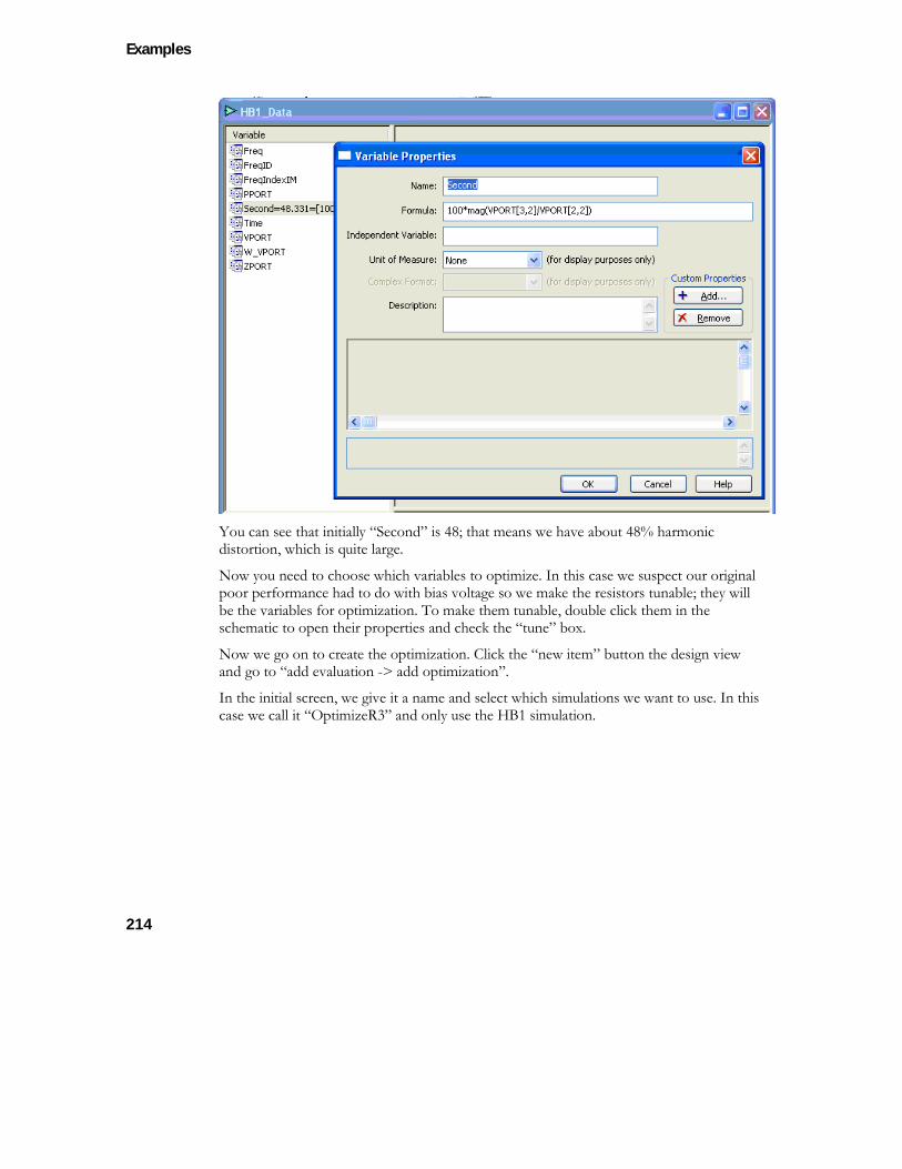
Examples
214
You can see that initially “Second” is 48; that means we have about 48% harmonic distortion, which is quite large.
Now you need to choose which variables to optimize. In this case we suspect our original poor performance had to do with bias voltage so we make the resistors tunable; they will be the variables for optimization. To make them tunable, double click them in the schematic to open their properties and check the “tune” box.
Now we go on to create the optimization. Click the “new item” button the design view and go to “add evaluation -> add optimization”.
In the initial screen, we give it a name and select which simulations we want to use. In this case we call it “OptimizeR3” and only use the HB1 simulation.
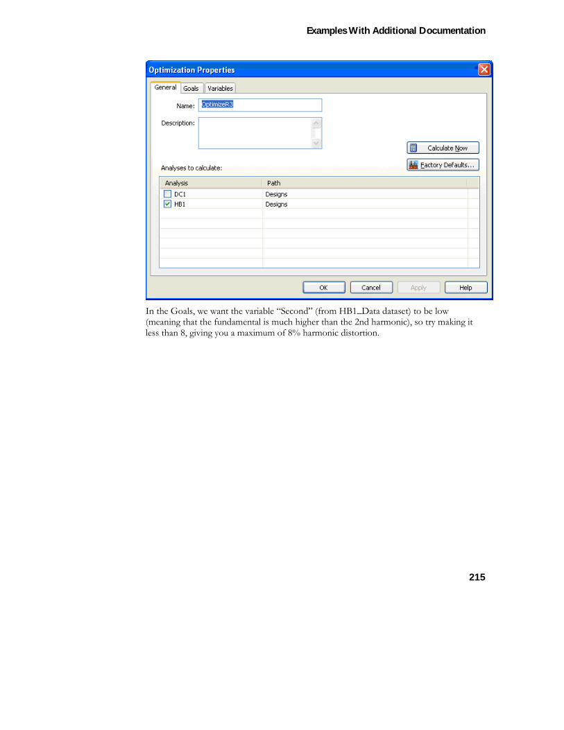
Examples With Additional Documentation
215
In the Goals, we want the variable “Second” (from HB1_Data dataset) to be low (meaning that the fundamental is much higher than the 2nd harmonic), so try making it less than 8, giving you a maximum of 8% harmonic distortion.
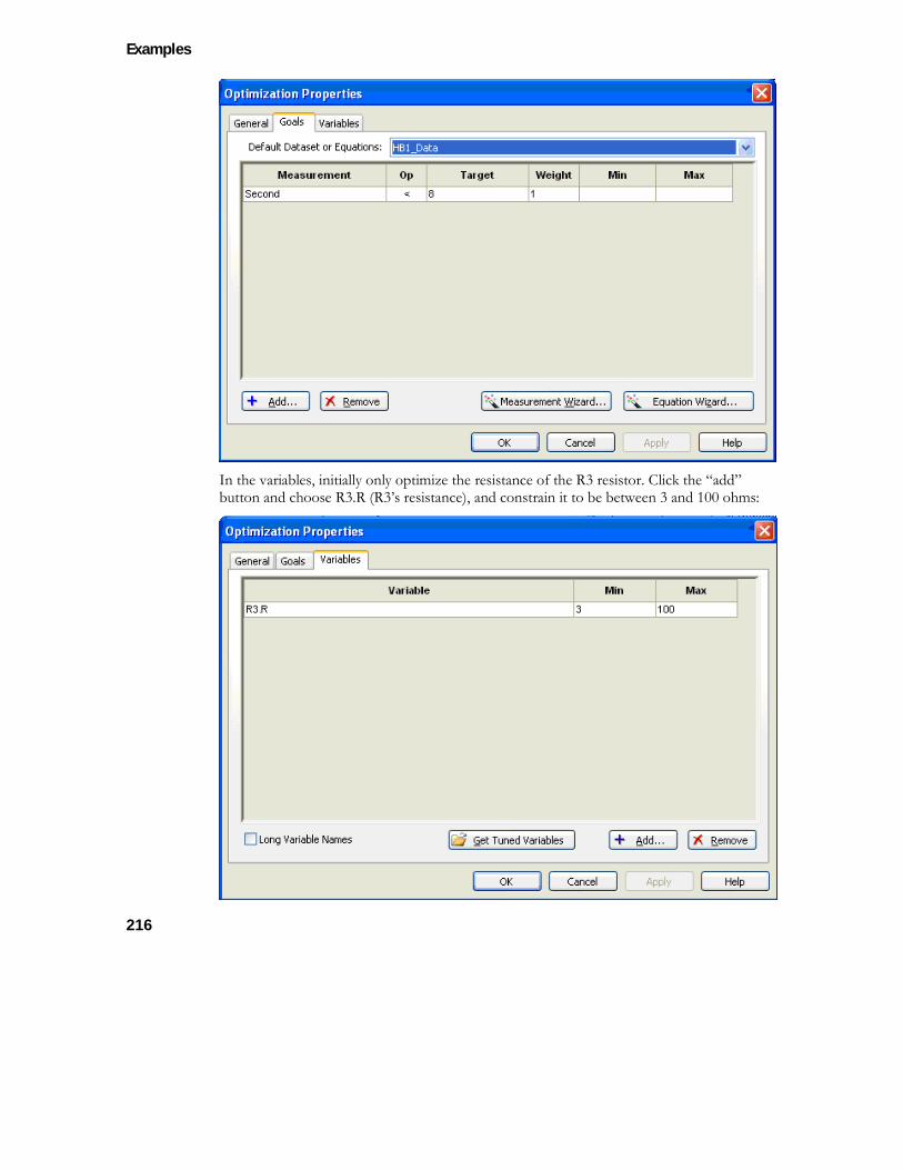
Examples
216
In the variables, initially only optimize the resistance of the R3 resistor. Click the “add” button and choose R3.R (R3’s resistance), and constrain it to be between 3 and 100 ohms:
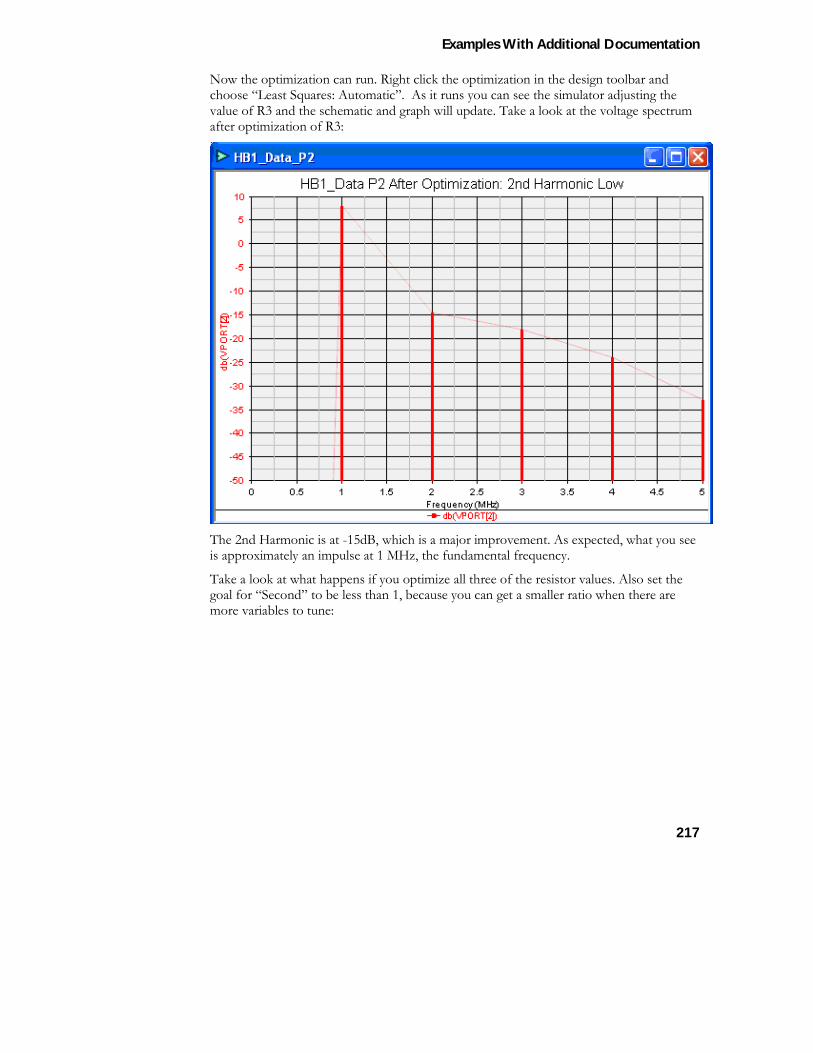
Examples With Additional Documentation
217
Now the optimization can run. Right click the optimization in the design toolbar and choose “Least Squares: Automatic”. As it runs you can see the simulator adjusting the value of R3 and the schematic and graph will update. Take a look at the voltage spectrum after optimization of R3:
The 2nd Harmonic is at -15dB, which is a major improvement. As expected, what you see is approximately an impulse at 1 MHz, the fundamental frequency.
Take a look at what happens if you optimize all three of the resistor values. Also set the goal for “Second” to be less than 1, because you can get a smaller ratio when there are more variables to tune:
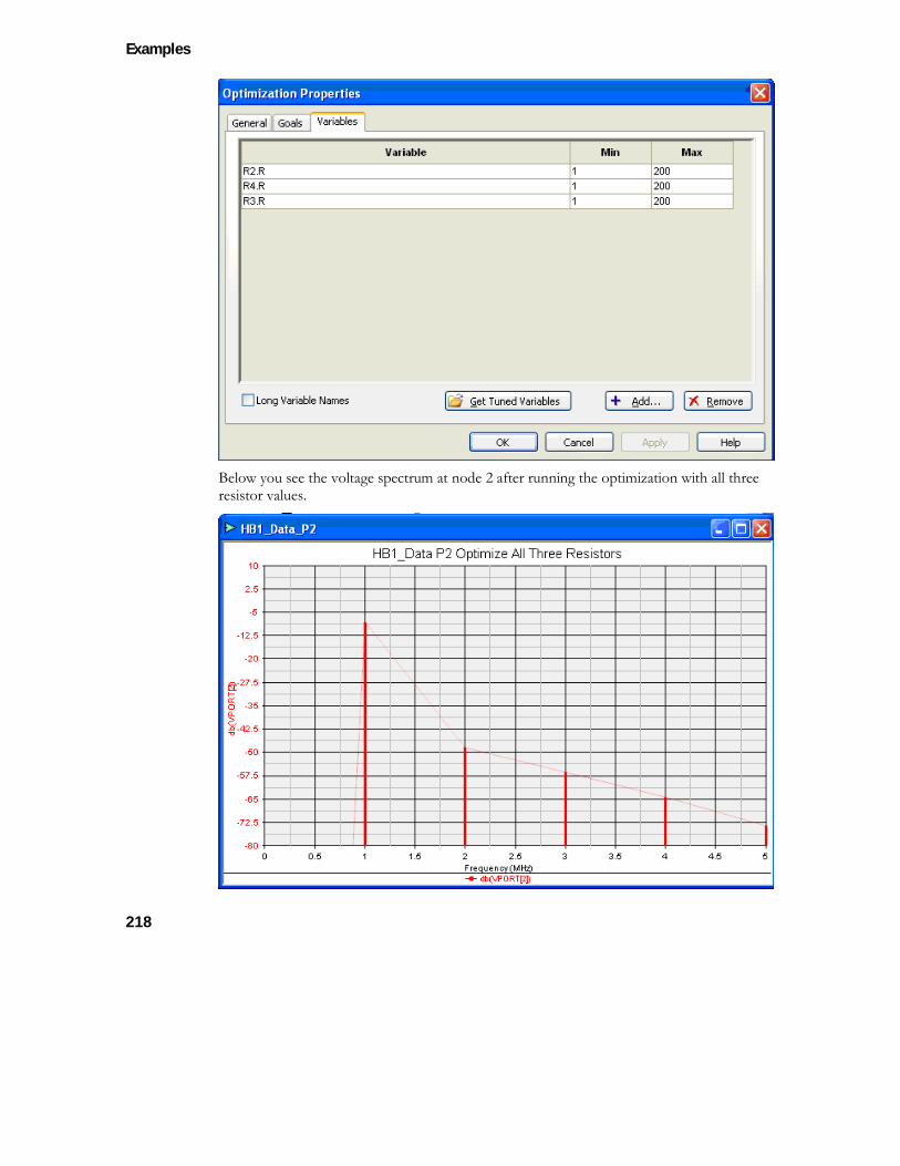
Examples
218
Below you see the voltage spectrum at node 2 after running the optimization with all three resistor values.
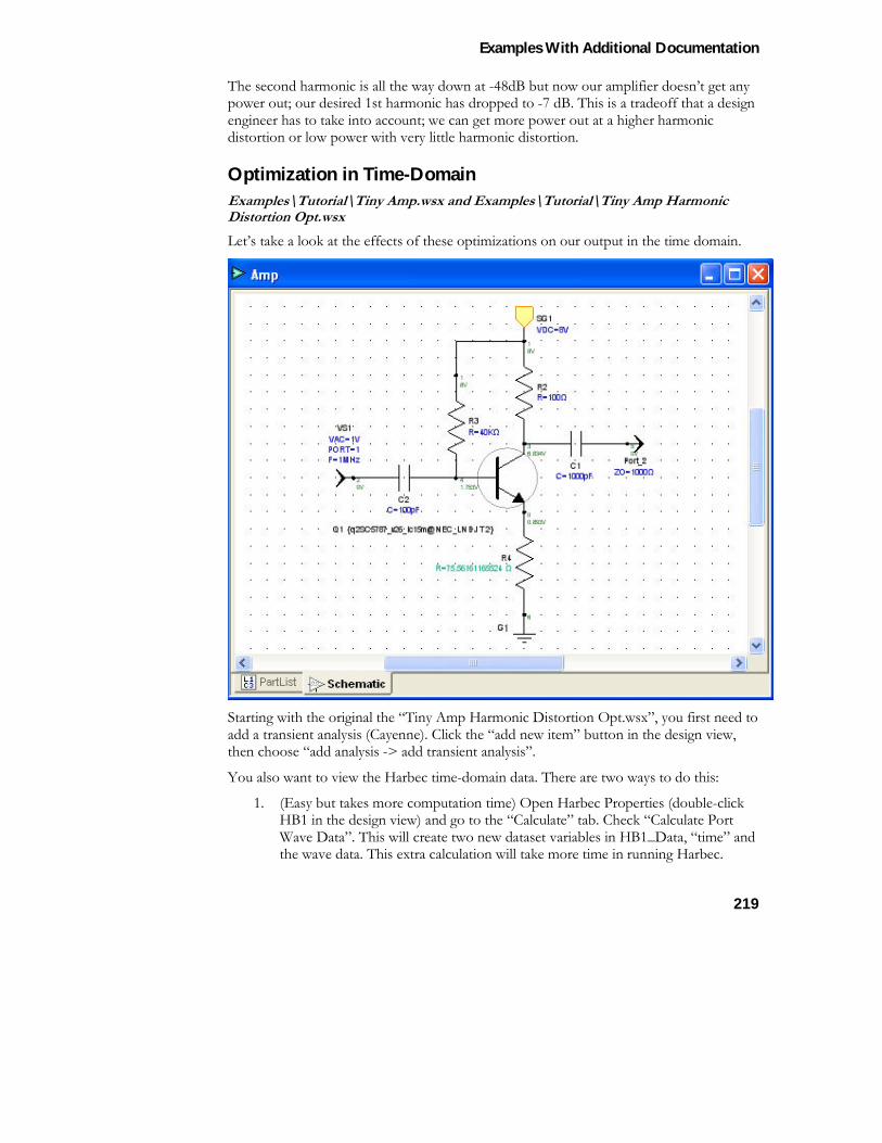
Examples With Additional Documentation
219
The second harmonic is all the way down at -48dB but now our amplifier doesn’t get any power out; our desired 1st harmonic has dropped to -7 dB. This is a tradeoff that a design engineer has to take into account; we can get more power out at a higher harmonic distortion or low power with very little harmonic distortion.
Optimization in Time-Domain Examples\Tutorial\Tiny Amp.wsx and Examples\Tutorial\Tiny Amp Harmonic Distortion Opt.wsx Let’s take a look at the effects of these optimizations on our output in the time domain.
Starting with the original the “Tiny Amp Harmonic Distortion Opt.wsx”, you first need to add a transient analysis (Cayenne). Click the “add new item” button in the design view, then choose “add analysis -> add transient analysis”.
You also want to view the Harbec time-domain data. There are two ways to do this:
1. (Easy but takes more computation time) Open Harbec Properties (double-click HB1 in the design view) and go to the “Calculate” tab. Check “Calculate Port Wave Data”. This will create two new dataset variables in HB1_Data, “time” and the wave data. This extra calculation will take more time in running Harbec.
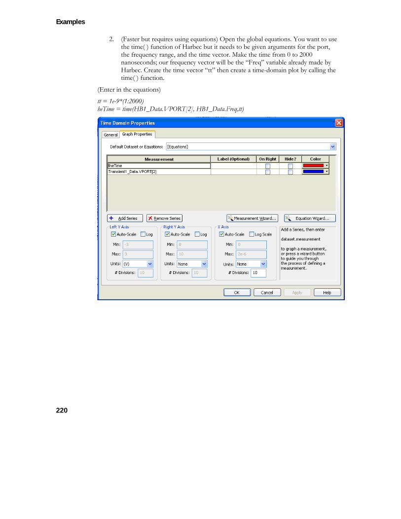
Examples
220
2. (Faster but requires using equations) Open the global equations. You want to use the time( ) function of Harbec but it needs to be given arguments for the port, the frequency range, and the time vector. Make the time from 0 to 2000 nanoseconds; our frequency vector will be the “Freq” variable already made by Harbec. Create the time vector “tt” then create a time-domain plot by calling the time( ) function.
(Enter in the equations)
tt = 1e-9*(1:2000) heTime = time(HB1_Data.VPORT[2], HB1_Data.Freq,tt)
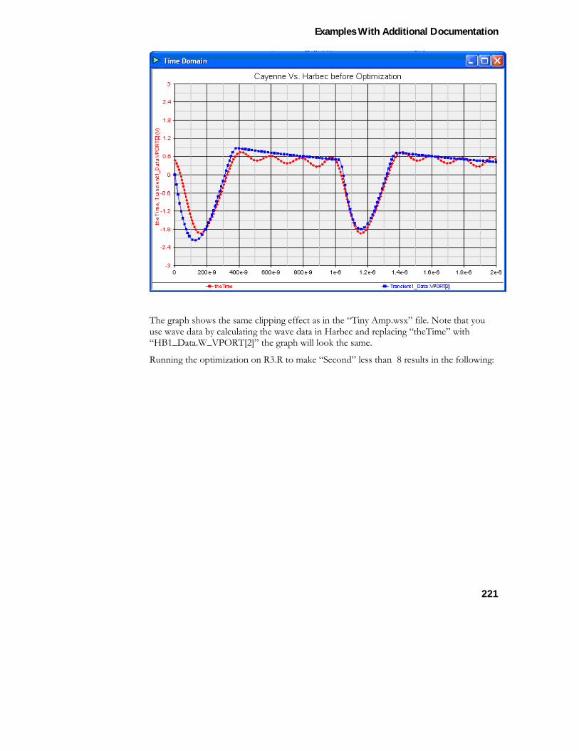
Examples With Additional Documentation
221
The graph shows the same clipping effect as in the “Tiny Amp.wsx” file. Note that you use wave data by calculating the wave data in Harbec and replacing “theTime” with “HB1_Data.W_VPORT[2]” the graph will look the same.
Running the optimization on R3.R to make “Second” less than 8 results in the following:
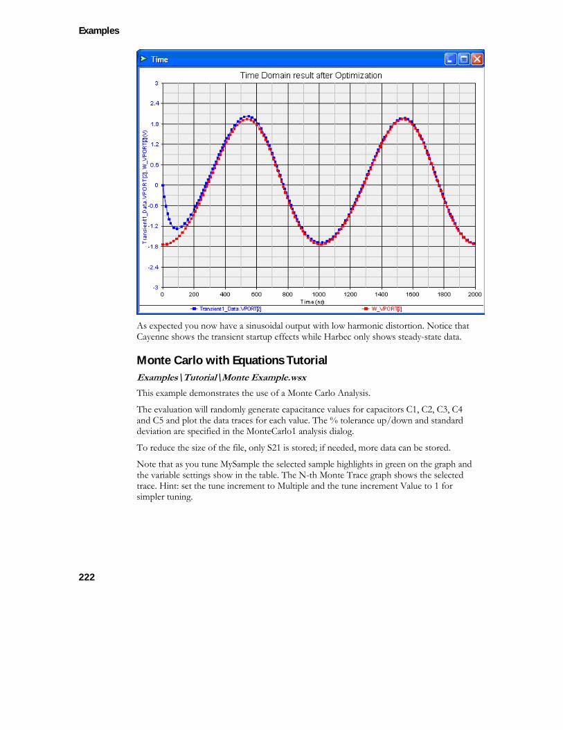
Examples
222
As expected you now have a sinusoidal output with low harmonic distortion. Notice that Cayenne shows the transient startup effects while Harbec only shows steady-state data.
Monte Carlo with Equations Tutorial Examples\Tutorial\Monte Example.wsx This example demonstrates the use of a Monte Carlo Analysis.
The evaluation will randomly generate capacitance values for capacitors C1, C2, C3, C4 and C5 and plot the data traces for each value. The % tolerance up/down and standard deviation are specified in the MonteCarlo1 analysis dialog.
To reduce the size of the file, only S21 is stored; if needed, more data can be stored.
Note that as you tune MySample the selected sample highlights in green on the graph and the variable settings show in the table. The N-th Monte Trace graph shows the selected trace. Hint: set the tune increment to Multiple and the tune increment Value to 1 for simpler tuning.
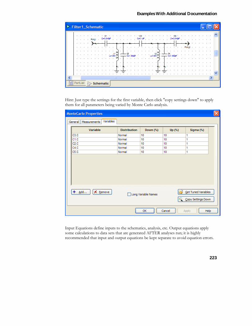
Examples With Additional Documentation
223
Hint: Just type the settings for the first variable, then click "copy settings down" to apply them for all parameters being varied by Monte Carlo analysis.
Input Equations define inputs to the schematics, analysis, etc. Output equations apply some calculations to data sets that are generated AFTER analyses run; it is highly recommended that input and output equations be kept separate to avoid equation errors.
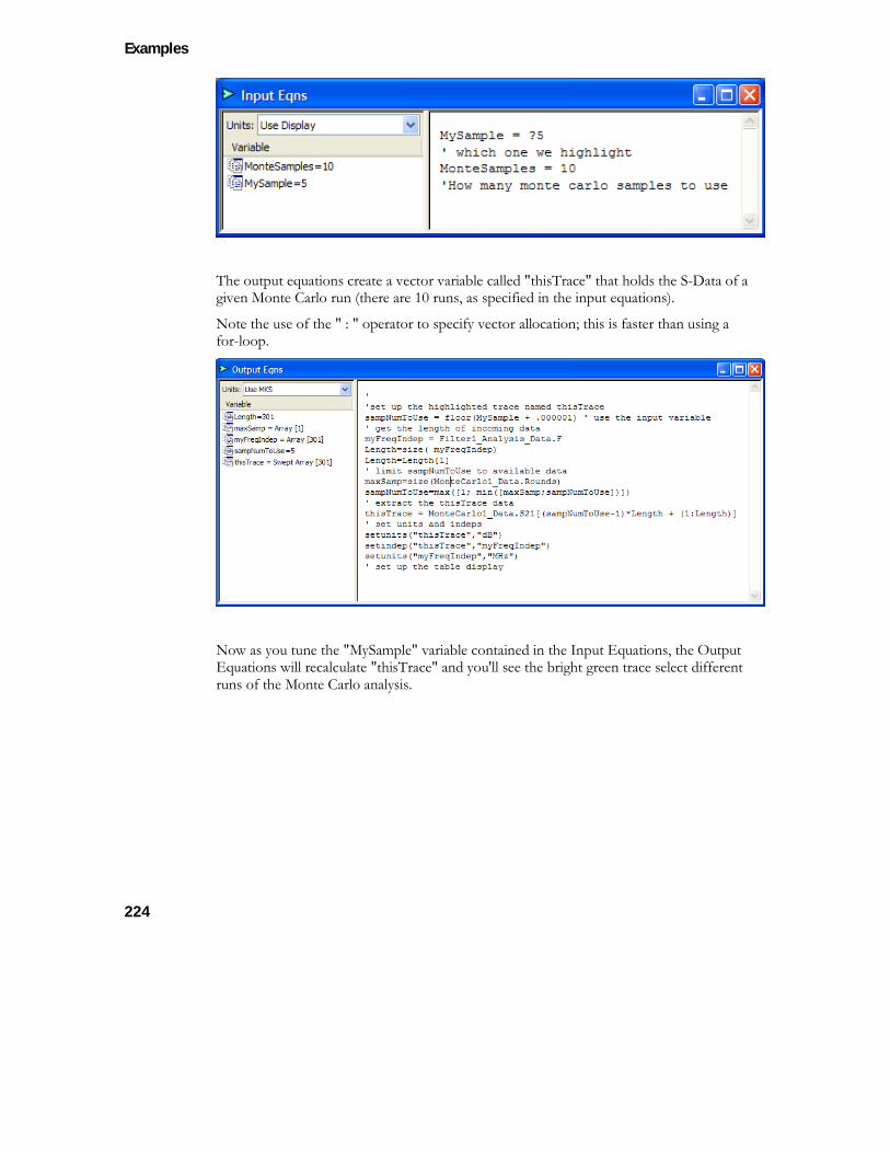
Examples
224
The output equations create a vector variable called "thisTrace" that holds the S-Data of a given Monte Carlo run (there are 10 runs, as specified in the input equations).
Note the use of the " : " operator to specify vector allocation; this is faster than using a for-loop.
Now as you tune the "MySample" variable contained in the Input Equations, the Output Equations will recalculate "thisTrace" and you'll see the bright green trace select different runs of the Monte Carlo analysis.
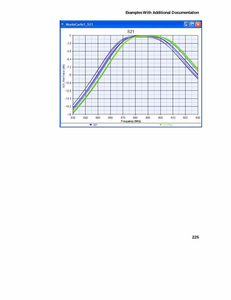
Examples With Additional Documentation
225

227
Index
2 2-section microstrip combline ........................ 117
3 3-section edge-coupled..................................... 108
4 4-inductor extractions....................................... 136
8 8 way.wsp ............................................................ 169
A agile antenna.wsp................................................. 71 all parallel resonators example ............... 138, 140 all series resonators example ........................... 152 all-pole ................................................................. 144 Alta Frequenza ................................................... 149 amp feedback.wsp ............................................... 48 amp noise.wsp...................................................... 50 amplifier tuned.wsp............................................. 59 amplifier.wsp ..................................................59, 61 amplifiers......................................... 54, 59, 61, 158 antenna ..................................................... 71, 78, 80 antennas, MAmmannPatch.wsp....................... 78 array driver.wsp.................................................... 75 attenuators ................................................. 180, 182
B balanced amp.wsp ............................................... 54 bandpass filter, Edge Coupled........................ 123 bandpass filter, Edge Redundant ................... 125 box.......................................................................... 84 box modes.................................................. 108, 169 box modes.wsp .................................................... 90 branch line .......................................................... 178 Butterworth filter............................................... 144
C calculate N ................................................. 130, 149
calculate N to remove existing transformers149 capacitors ....................................................140, 156 Carassa................................................................. 149 cell size ...................................................................84 Chebyshev ..................................................106, 144 Chebyshev coupled-resonator ........................ 144 circles ...............................................................50, 63 circuit co-simulation ............................................61 Combline ............................................................ 117 computer simulation......................................... 149 contiguous diplexer.wsp .................................. 106 convert using advanced TLINE..................... 158 co-simulation.........................................................80 coupled lines....................................................... 108 coupled-line ........................................................ 178 crystal...........................................................121, 157 customizing
Equal Termination Example ..................... 130
D deembedding...................................................... 108 detector ..................................................................98 detectors/simple detector.wsp ..........................98 dielectric .............................................................. 140 dielectric constant ............................................. 140 DIODE..................................................................98 diode detector circuit...........................................98 diplexers .............................................................. 106 dipole antenna.......................................................80 dual mode coupler.wsp .................................... 175
E edge coupled ..............................................108, 123 edge coupler.wsp ............................................... 178 edge redundant .................................................. 125 EdgeCoupledBenchmark.wsp ........................ 108 EdgeCoupledOpened.wsp .............................. 108 Edit menu ..............................................................54 electromagnetic.................................................. 144 electromagnetic simulation.................................61 EM ..........................................................................61 equal inductor example .................................... 129 equal termination example .............................. 130 extraction goals .................................................. 136 extraction sequence...................................140, 149 extractions................................. 130, 140, 144, 149

Examples
228
Extractions tab................................................... 136
F feed forward amplifier...................................... 186 film ....................................................................... 180 FILTER...................................................... 111, 144 finite zeros ................................................. 144, 149 force symmetry .................................................. 144
G group delay ......................................................... 149 group-delay characteristics .............................. 149
H HF filter design.................................................. 149 high-Q quartz-crystal resonators.................... 152 how to design filters.......................................... 157
I inductor Q .......................................................... 144 inductor, equal example ................................... 129 infinity......................................................... 140, 149 instability ............................................................... 63 interdigital ........................................................... 117 interdigital.wsp ................................................... 113 internal ports ..................................................80, 84
L lower stopbands................................................. 140 lowpass ................................................................ 149
M MATCH.............................................................. 158 maximum realizability example ...................... 136 measured data........................................ 78, 87, 180 measuring S-parameters ..................................... 87 microwave circuits............................................... 50 MIXER................................................................ 161 mixer/low power mixer.wsp........................... 161
N NET block
Balanced AMP................................................ 54 noise circles........................................................... 50 noise figure ........................................................... 50 nonlinear models ................................................. 87
non-resonant simulation..........................113, 117 Norton ........................................................140, 149 Norton series .................. 129, 130, 138, 140, 149 Norton shunt .............................................129, 152 Norton transforms....................................129, 144
O odd-order Chebyshev........................................144 optimization .........................50, 87, 140, 144, 156 output matching ...................................................50
P parameter sweeps .................................................98 parameters
parametric bandpass example.....................140 parametric bandpass example..........................140 passband ripple...................................................140 patch antenna........................................................78 permutation................................................130, 136 physical symmetry..............................................144 physical symmetry example..............................144 poor stopband performance ..............................90 power amp...........................................................158 prob-fed antenna..................................................78
Q quad hybrid matrix amp....................................190 quarter-wave........................................................140 quartz-crystal resonators...................................152
R reference plane....................................................108 remove existing transformer............................149 remove sidewall reactances ................................61 remove transformer...........................................136 resonator Q .........................................................136 resonators ................113, 136, 140, 144, 156, 157 response symmetry example ............................149
S series element first ....................................138, 152 shunt-coupling ....................................................144 sidelobes.................................................................75 signal control/ResistiveBroadband20dB.wsp
..........................................................................182 simple dipole.wsp.................................................80 simplify........................................................129, 149 simplify circuit ...........................................138, 149 single-ended ..........................................................54
Index
229
singly-terminated ............................................... 106 solid thinning...................................................... 180 specifications ...................................................... 138 Specifications tab...................................... 144, 149 SPECTRASYS .......................................... 186, 190 SPICE
comparing and optimizing............................ 87 stability.............................................................63, 90 stopband performance ....................................... 90 stub with inverters............................................. 127 subsections............................................................ 90 symmetrical ................................................ 144, 149
T termination coupling example......................... 156 thin film attenuator ........................................... 180 thin loop antenna................................................. 84 thin loop.wsp........................................................ 84 top cover ............................................................... 90 transformations......................................... 140, 156 transformer ......................136, 140, 144, 149, 156 transformer ratio....................................... 144, 149 transformers .............................................. 129, 184
transforms................................. 129, 144, 149, 156 tuned bandpass filter ........................................ 117
U upper cutoff........................................................ 156 upper stopband.................................................. 140
V varactor .........................................................71, 117 viewer .................................................................. 175
W Wilkinson....................................................169, 178
X Xfmr coupler.wsp ............................................. 184 Xtal filter.wsp..................................................... 121