Embed Size (px)
Citation preview
Facility of Engineering
Biomedical Engineering Department
Medical Electronic Lab
BME (317)
Post-lab Forms
Prepared by Eng.Hala Amari Spring 2014
Facility of Engineering
Biomedical Engineering Department
Medical Electronic Lab
BME (317)
EXP#2: Diode Characteris cs & Applica ons
Post-Report
Student Name:
Student Number:
Submission Date:
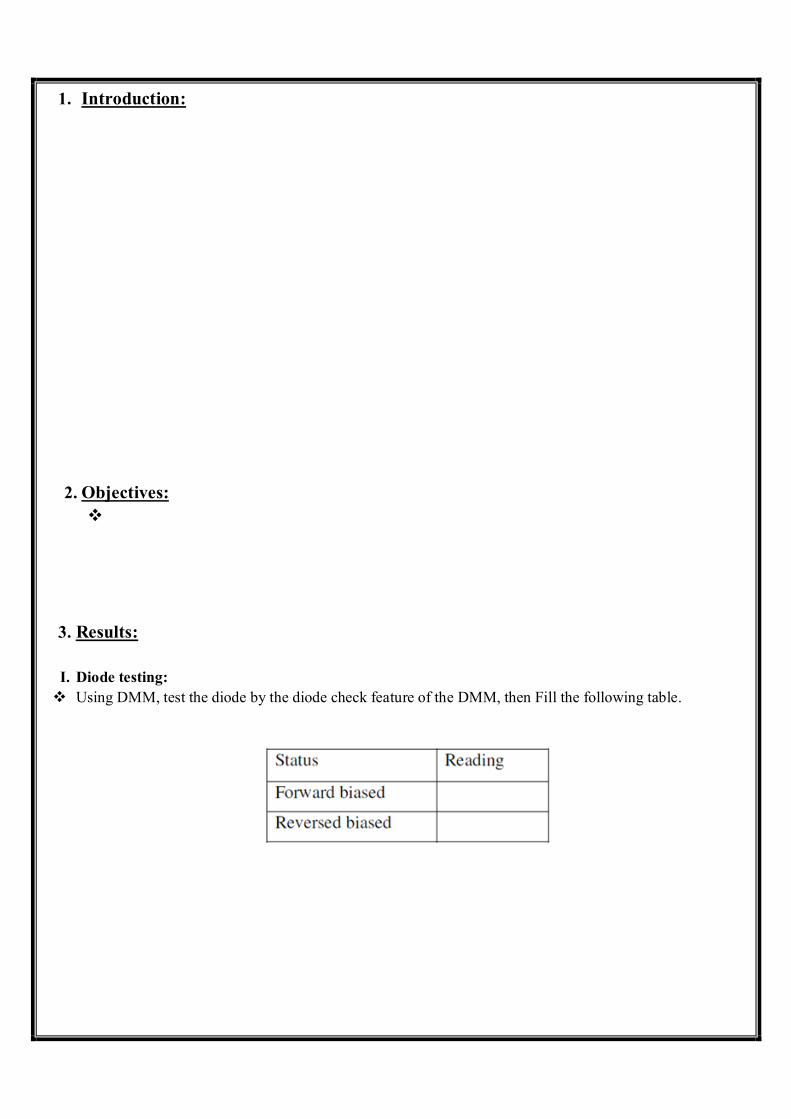
1. Introduction:
2. Objectives:
3. Results:
I. Diode testing: Using DMM, test the diode by the diode check feature of the DMM, then Fill the following table.
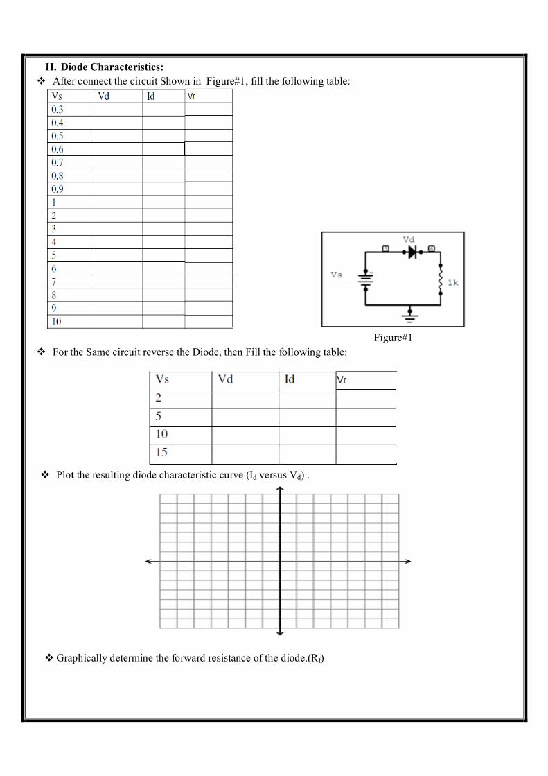
II. Diode Characteristics: After connect the circuit Shown in Figure#1, fill the following table:
Figure#1
For the Same circuit reverse the Diode, then Fill the following table:
Plot the resulting diode characteristic curve (Id versus Vd) .
Graphically determine the forward resistance of the diode.(Rf)
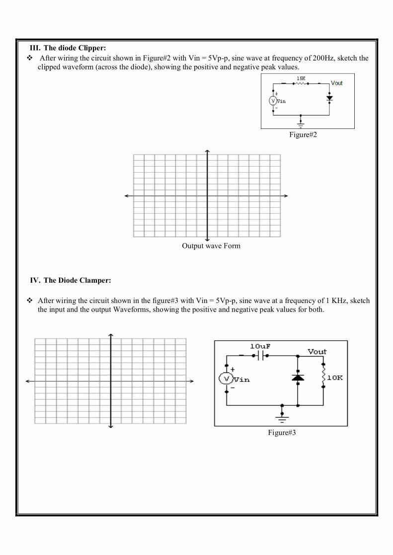
III. The diode Clipper: After wiring the circuit shown in Figure#2 with Vin = 5Vp-p, sine wave at frequency of 200Hz, sketch the
clipped waveform (across the diode), showing the positive and negative peak values.
Figure#2
Output wave Form
IV. The Diode Clamper:
After wiring the circuit shown in the figure#3 with Vin = 5Vp-p, sine wave at a frequency of 1 KHz, sketch the input and the output Waveforms, showing the positive and negative peak values for both.
Figure#3
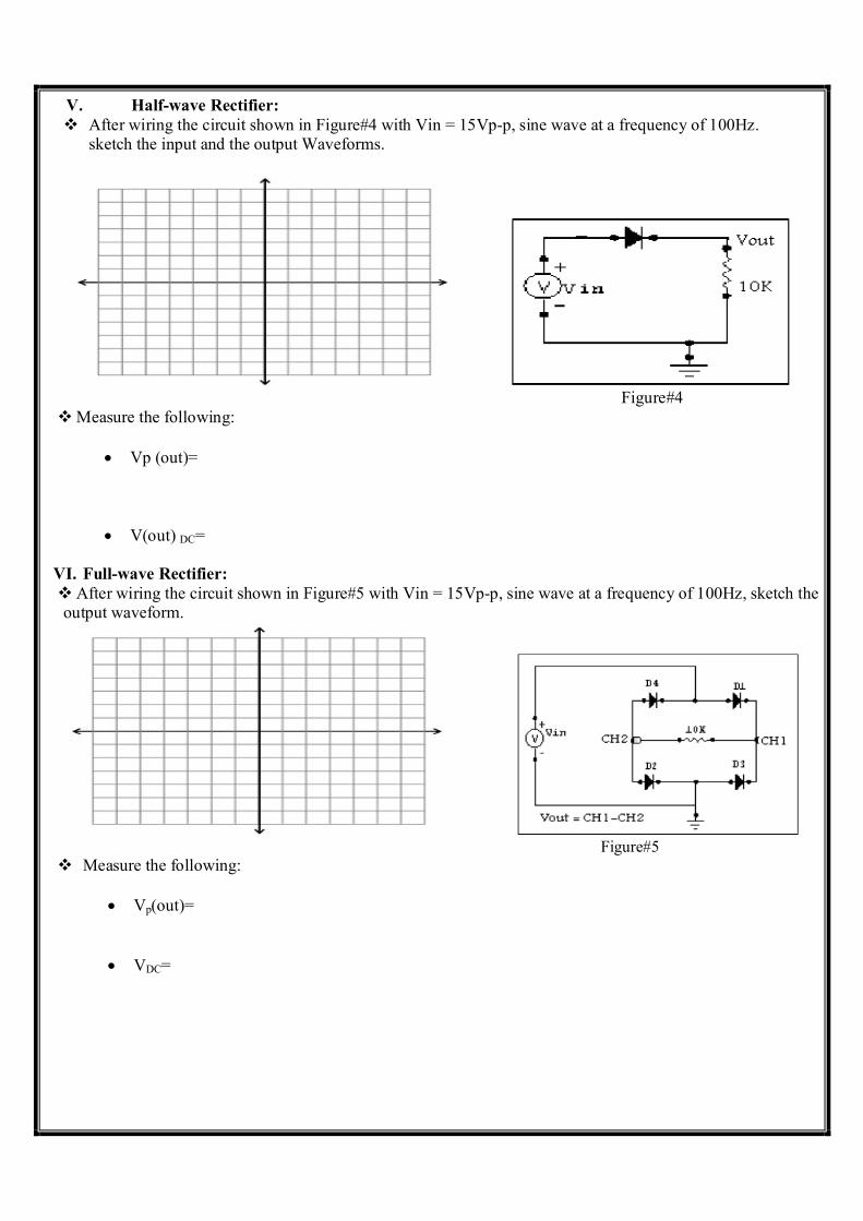
V. Half-wave Rectifier: After wiring the circuit shown in Figure#4 with Vin = 15Vp-p, sine wave at a frequency of 100Hz.
sketch the input and the output Waveforms.
Figure#4
Measure the following:
Vp (out)=
V(out) DC=
VI. Full-wave Rectifier: After wiring the circuit shown in Figure#5 with Vin = 15Vp-p, sine wave at a frequency of 100Hz, sketch the output waveform.
Figure#5
Measure the following:
Vp(out)=
VDC=
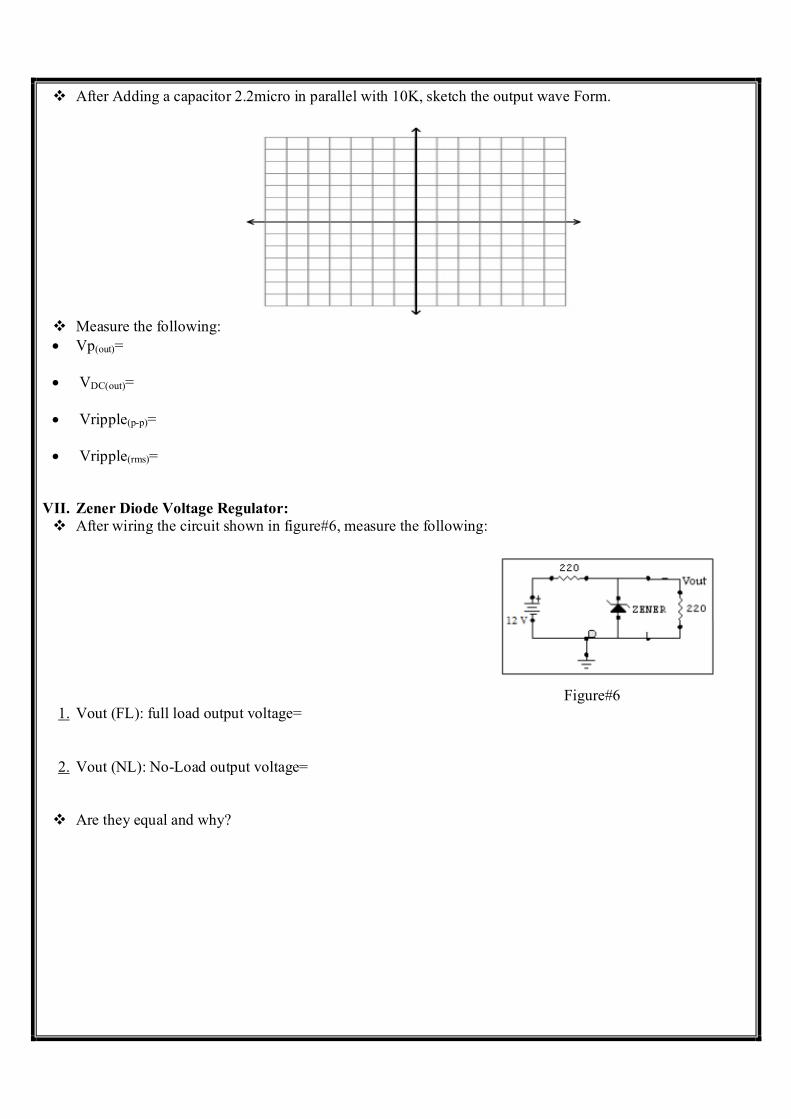
After Adding a capacitor 2.2micro in parallel with 10K, sketch the output wave Form.
Measure the following: Vp(out)=
VDC(out)=
Vripple(p-p)=
Vripple(rms)=
VII. Zener Diode Voltage Regulator: After wiring the circuit shown in figure#6, measure the following:
Figure#6
1. Vout (FL): full load output voltage=
2. Vout (NL): No-Load output voltage=
Are they equal and why?

4. Conclusion and discussion:
Facility of Engineering
Biomedical Engineering Department
Medical Electronic Lab
BME (317)
EXP#3: Common Emitter Characteristics & Amplifier
Post-Report
Student Name:
Student Number:
Submission Date:
1. Introduction:
2. Objectives:
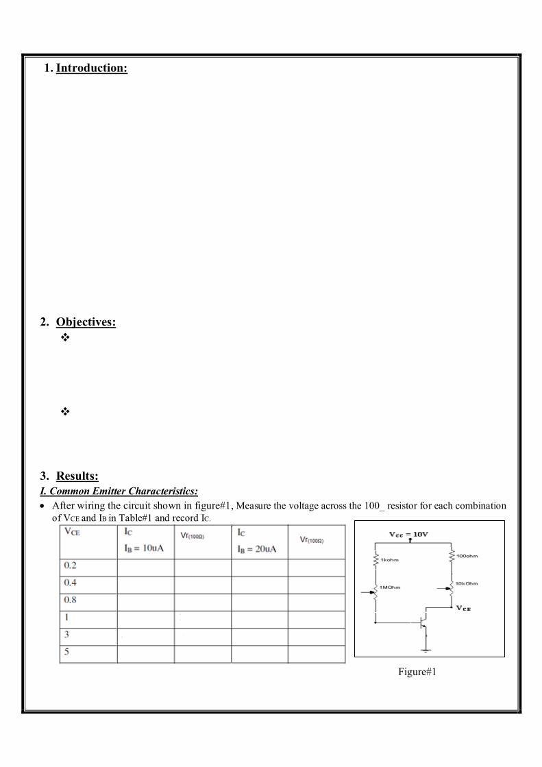
3. Results: I. Common Emitter Characteristics: After wiring the circuit shown in figure#1, Measure the voltage across the 100_ resistor for each combination
of VCE and IB in Table#1 and record IC.
Figure#1
Plot the output characteristics of the common emitter bias circuit (IC vs VCE).
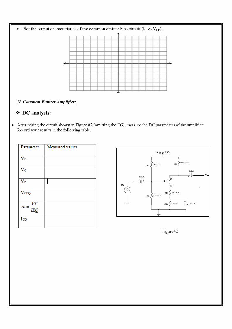
II. Common Emitter Amplifier: DC analysis:
After wiring the circuit shown in Figure #2 (omitting the FG), measure the DC parameters of the amplifier:
Record your results in the following table.
Figure#2
AC Analysis:
Connect the FG as shown in Figure # 2 and adjust the sine wave output of the FG at 200mVp-p and a frequency of I0kHz. Measure and record the peak-to-peak output voltage Vo for the following conditions:
What is the phase shift between the input signal and the output signal?
Measure the following parameter for the Normal circuit: 1. Ro=
2. Rin=
3. FH=
4. Fl=
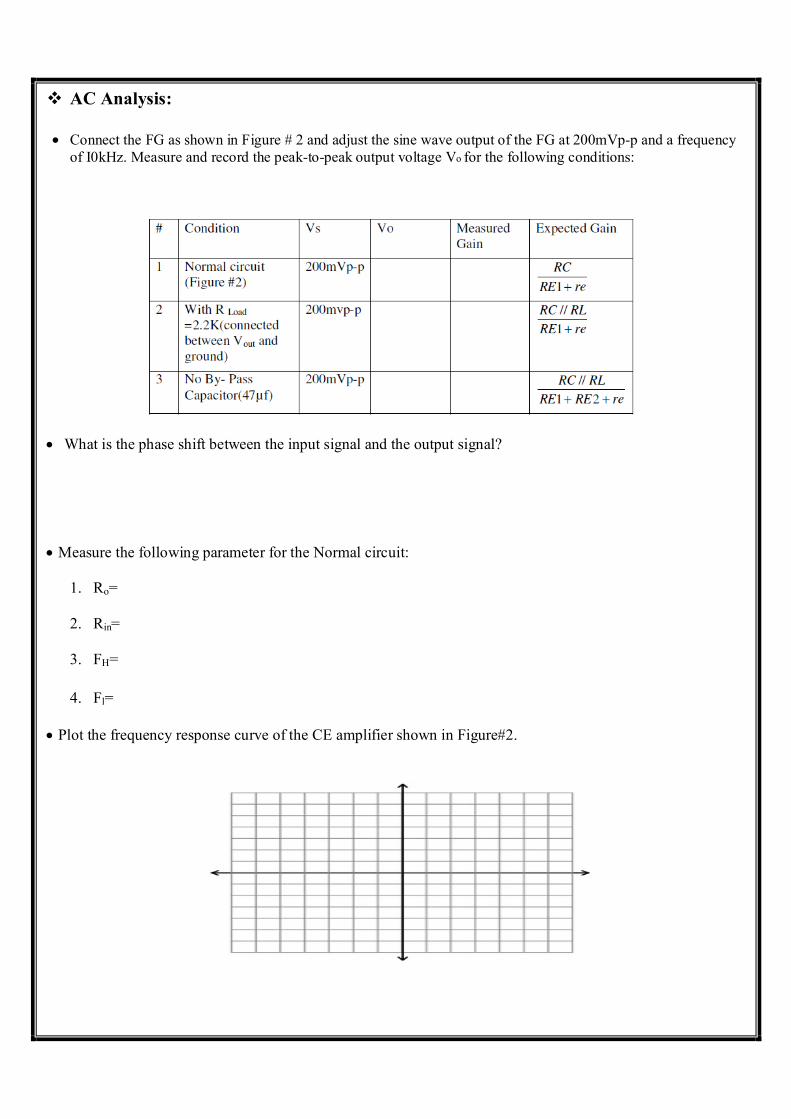
Plot the frequency response curve of the CE amplifier shown in Figure#2.

4. Conclusion and discussion:
Facility of Engineering
Biomedical Engineering Department
Medical Electronic Lab
BME (317)
EXP#4: JFET Characteristics and Applications
Post-Report
Student Name:
Student Number:
Submission Date:
1. Introduction:
2. Objectives:
3. Results:
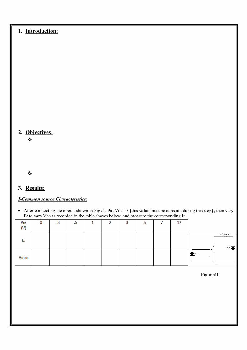
I-Common source Characteristics:
After connecting the circuit shown in Fig#1. Put VGS =0 this value must be constant during this step, then vary E2 to vary VDS as recorded in the table shown below, and measure the corresponding ID.
Figure#1
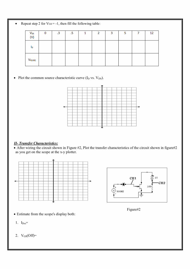
Repeat step 2 for VGS = -1, then fill the following table:
Plot the common source characteristic curve (ID vs. VDS).
II- Transfer Characteristics: After wiring the circuit shown in Figure #2, Plot the transfer characteristics of the circuit shown in figure#2 as you get on the scope at the x-y plotter.
Figure#2 Estimate from the scope's display both: 1. IDss=
2. VGS(Off)=
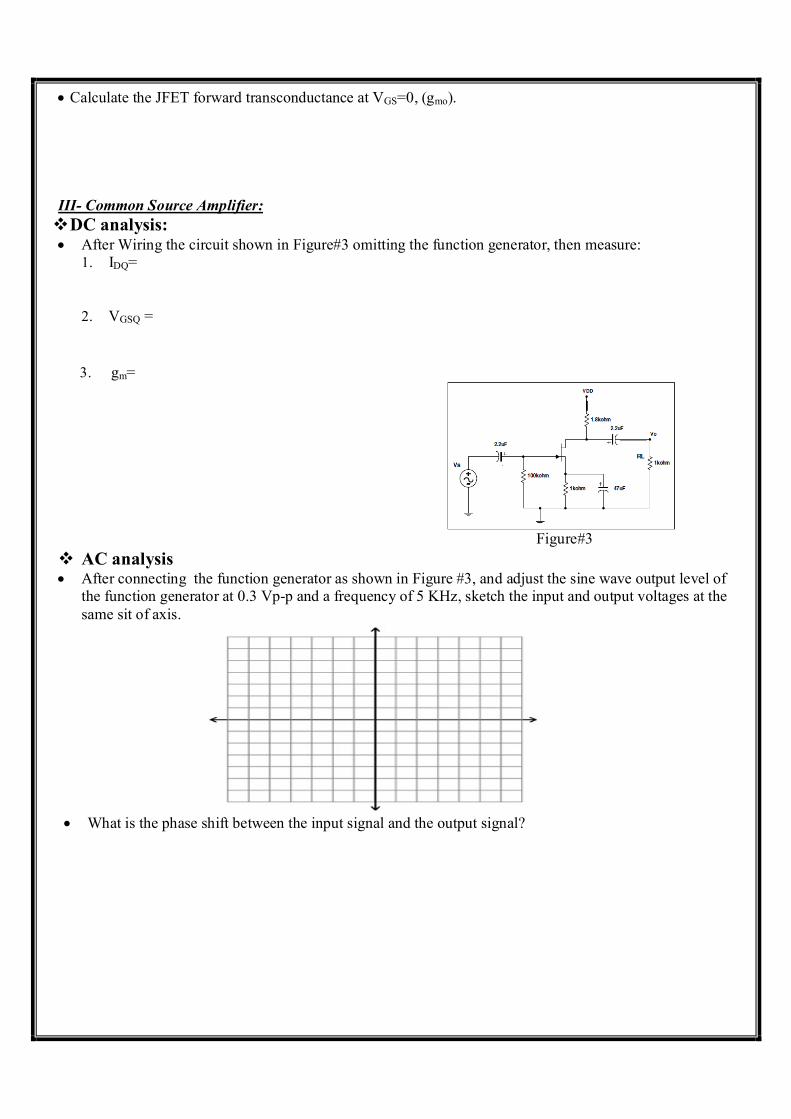
Calculate the JFET forward transconductance at VGS=0, (gmo).
III- Common Source Amplifier: DC analysis: After Wiring the circuit shown in Figure#3 omitting the function generator, then measure:
1. IDQ=
2. VGSQ =
3. gm=
Figure#3
AC analysis After connecting the function generator as shown in Figure #3, and adjust the sine wave output level of
the function generator at 0.3 Vp-p and a frequency of 5 KHz, sketch the input and output voltages at the same sit of axis.
What is the phase shift between the input signal and the output signal?
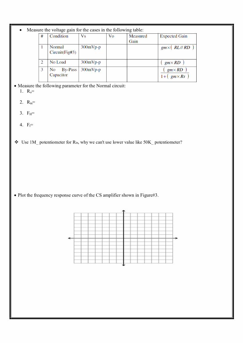
Measure the voltage gain for the cases in the following table:
Measure the following parameter for the Normal circuit:
1. Ro=
2. Rin=
3. FH=
4. Fl=
Use 1M_ potentiometer for Rin, why we can't use lower value like 50K_ potentiometer?
Plot the frequency response curve of the CS amplifier shown in Figure#3.

4. Conclusion and discussion:
Facility of Engineering
Biomedical Engineering Department
Medical Electronic Lab
BME (317)
EXP#5: Operational Amplifier Characteristics & Applications
Post-Report
Student Name:
Student Number:
Submission Date:
1. Introduction:
2. Objectives:
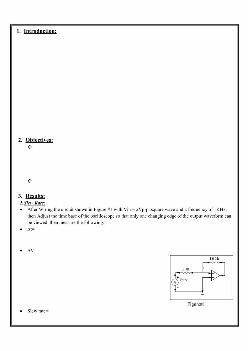
3. Results: I. Slew Rate: After Wiring the circuit shown in Figure #1 with Vin = 2Vp-p, square wave and a frequency of 1KHz,
then Adjust the time base of the oscilloscope so that only one changing edge of the output waveform can be viewed, then measure the following:
∆t=
∆V=
Figure#1
Slew rate=
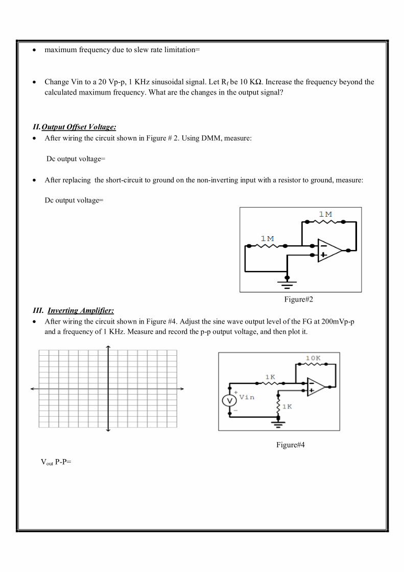
maximum frequency due to slew rate limitation=
Change Vin to a 20 Vp-p, 1 KHz sinusoidal signal. Let Rf be 10 KΩ. Increase the frequency beyond the calculated maximum frequency. What are the changes in the output signal?
II. Output Offset Voltage: After wiring the circuit shown in Figure # 2. Using DMM, measure:
Dc output voltage=
After replacing the short-circuit to ground on the non-inverting input with a resistor to ground, measure: Dc output voltage=
Figure#2
III. Inverting Amplifier: After wiring the circuit shown in Figure #4. Adjust the sine wave output level of the FG at 200mVp-p
and a frequency of 1 KHz. Measure and record the p-p output voltage, and then plot it.
Figure#4
Vout P-P=
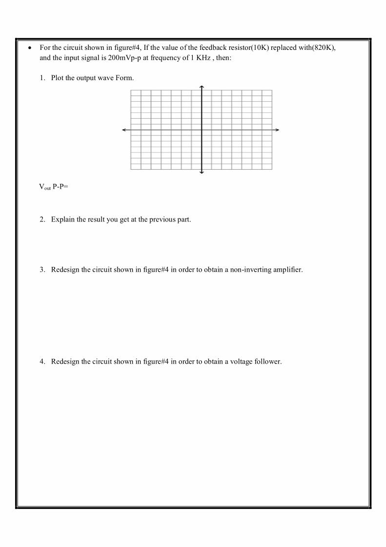
For the circuit shown in figure#4, If the value of the feedback resistor(10K) replaced with(820K), and the input signal is 200mVp-p at frequency of 1 KHz , then: 1. Plot the output wave Form.
Vout P-P=
2. Explain the result you get at the previous part.
3. Redesign the circuit shown in figure#4 in order to obtain a non-inverting amplifier.
4. Redesign the circuit shown in figure#4 in order to obtain a voltage follower.
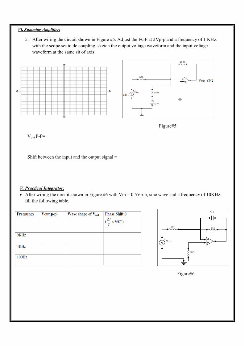
VI. Summing Amplifier:
5. After wiring the circuit shown in Figure #5. Adjust the FGF at 2Vp-p and a frequency of 1 KHz. with the scope set to dc coupling, sketch the output voltage waveform and the input voltage waveform at the same sit of axis .
Figure#5
Vout P-P=
Shift between the input and the output signal =
V. Practical Integrator: After wiring the circuit shown in Figure #6 with Vin = 0.5Vp-p, sine wave and a frequency of 10KHz,
fill the following table.
Figure#6
Measure the upper cutoff frequency of the circuit shown in Figure# 6 and draw the frequency response curve showing the value of the mid-band voltage gain and the cutoff frequency.
Upper cutoff frequency=
4. Conclusion and discussion:
Facility of Engineering
Biomedical Engineering Department
Medical Electronic Lab
BME (317)
EXP#6: Active Filters & Oscillators
Post-Report
Student Name:
Student Number:
Submission Date:
1. Introduction:
2. Objectives:
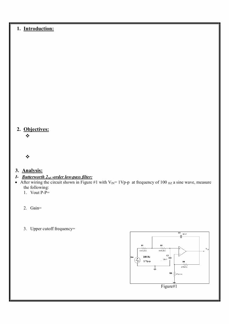
3. Analysis: I- Butterworth 2nd -order low-pass filter: After wiring the circuit shown in Figure #1 with VIN= 1Vp-p at frequency of 100 HZ a sine wave, measure
the following: 1. Vout P-P=
2. Gain=
3. Upper cutoff frequency=
Figure#1
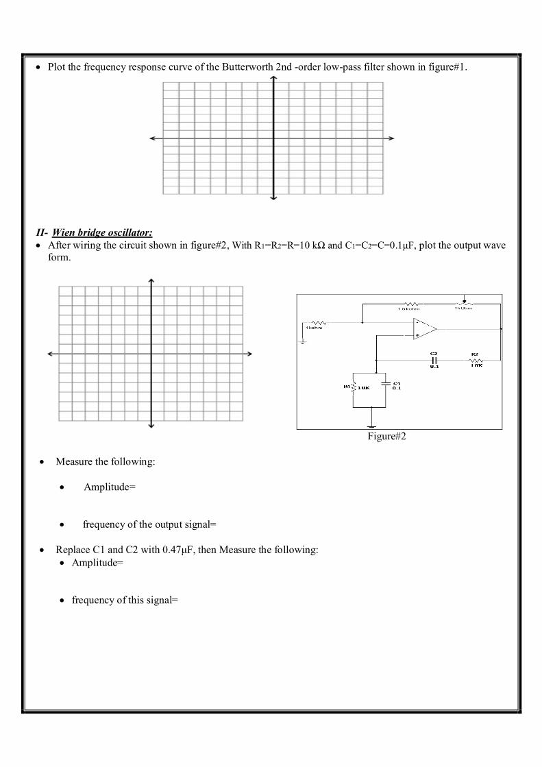
Plot the frequency response curve of the Butterworth 2nd -order low-pass filter shown in figure#1.
II- Wien bridge oscillator: After wiring the circuit shown in figure#2, With R1=R2=R=10 kΩ and C1=C2=C=0.1μF, plot the output wave
form.
Figure#2
Measure the following:
Amplitude= frequency of the output signal=
Replace C1 and C2 with 0.47μF, then Measure the following: Amplitude=
frequency of this signal=

4. Conclusion and discussion:
Facility of Engineering
Biomedical Engineering Department
Medical Electronic Lab
BME (317)
EXP#7: Transistors as Switching Elements (Inverters)
Post-Report
Student Name:
Student Number:
Submission Date:
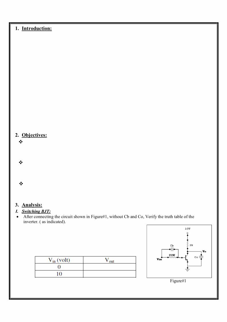
1. Introduction:
2. Objectives:
3. Analysis: I. Switching BJT: After connecting the circuit shown in Figure#1, without Cb and Co, Verify the truth table of the
inverter. ( as indicated).
Figure#1
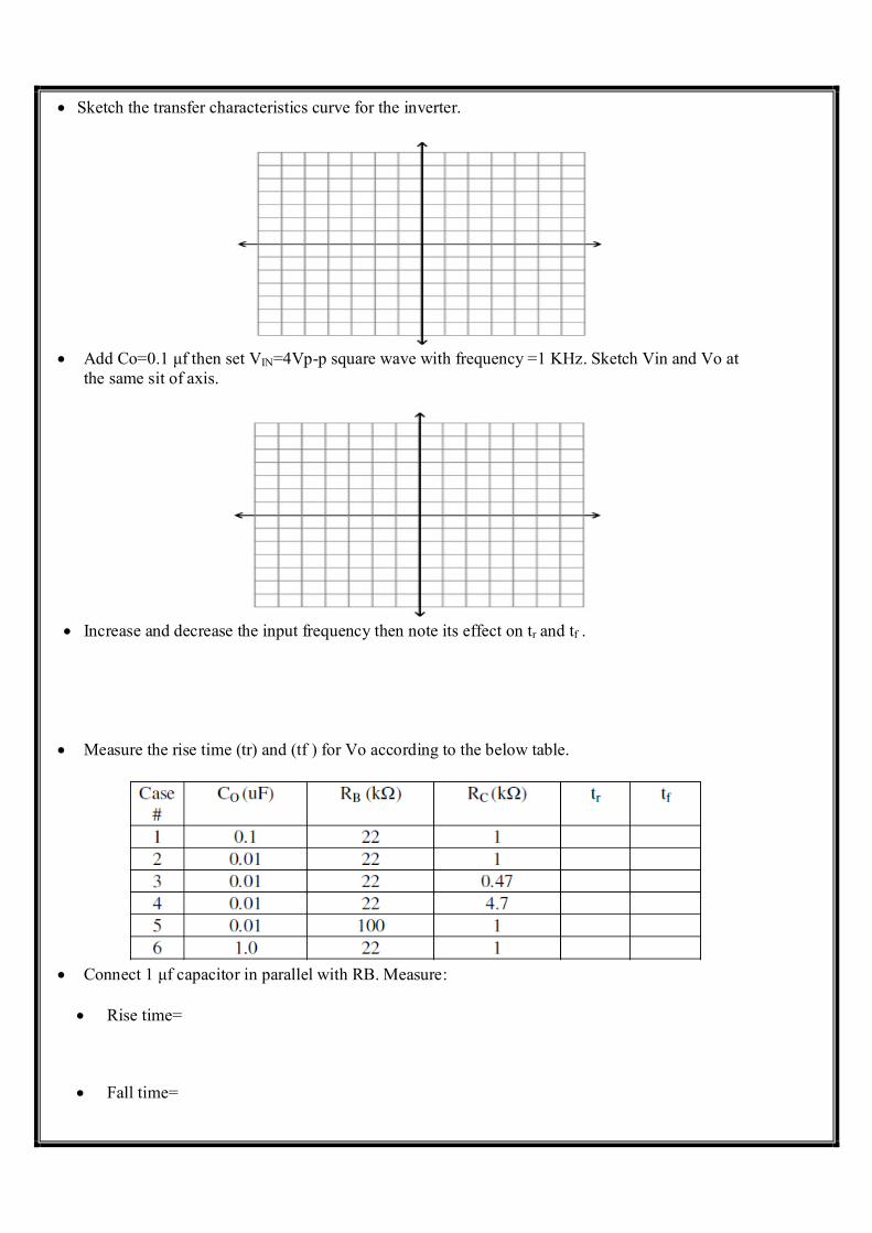
Sketch the transfer characteristics curve for the inverter.
Add Co=0.1 μf then set VIN=4Vp-p square wave with frequency =1 KHz. Sketch Vin and Vo at
the same sit of axis.
Increase and decrease the input frequency then note its effect on tr and tf .
Measure the rise time (tr) and (tf ) for Vo according to the below table.
Connect 1 μf capacitor in parallel with RB. Measure:
Rise time=
Fall time=
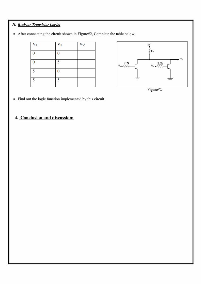
II. Resistor Transistor Logic:
After connecting the circuit shown in Figure#2, Complete the table below.
Figure#2
Find out the logic function implemented by this circuit.
4. Conclusion and discussion:
Facility of Engineering
Biomedical Engineering Department
Medical Electronic Lab
BME (317)
EXP#8: TTL and CMOS Logic Gates & Interfacing
Post-Report
Student Name:
Student Number:
Submission Date:
1. Introduction:
2. Objectives:
3. Analysis: III- TTL Driving Low-Voltage CMOS: After connecting the circuit shown in Figure#1 without the pull-up resistor RP. Complete the following table:
Figure#1
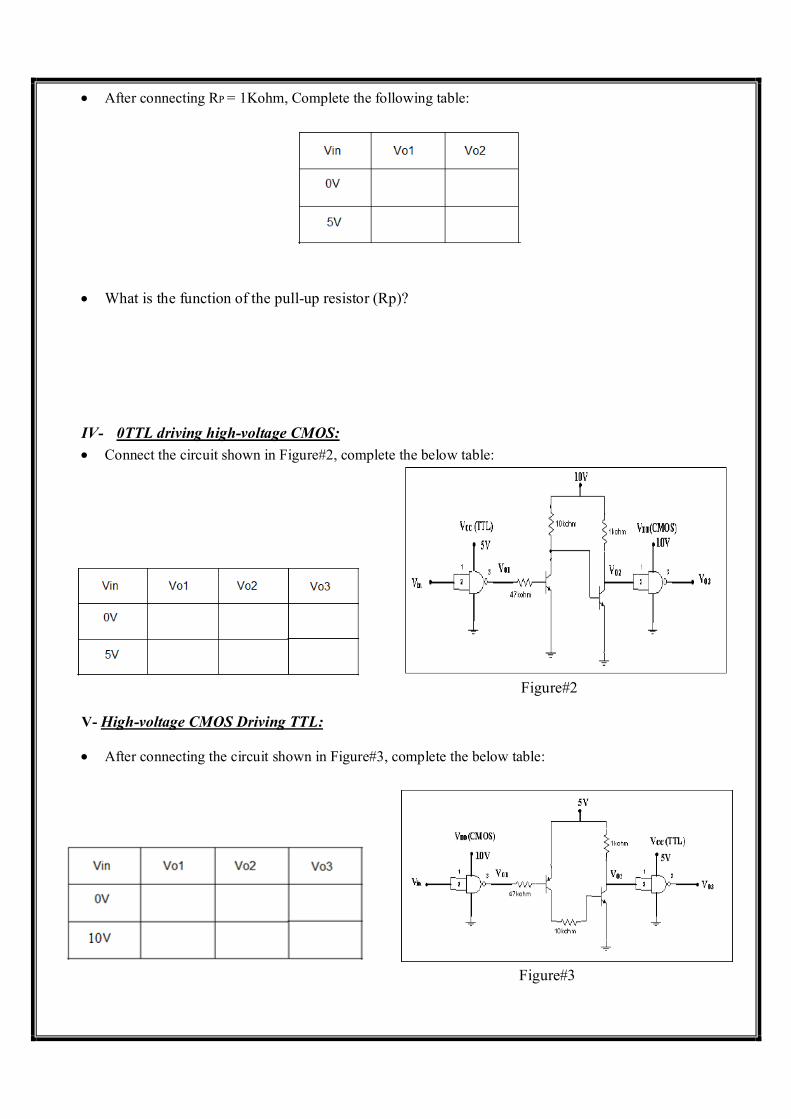
After connecting RP = 1Kohm, Complete the following table:
What is the function of the pull-up resistor (Rp)?
IV- 0TTL driving high-voltage CMOS: Connect the circuit shown in Figure#2, complete the below table:
Figure#2
V- High-voltage CMOS Driving TTL:
After connecting the circuit shown in Figure#3, complete the below table:
Figure#3

4. Conclusion and discussion:
Facility of Engineering
Biomedical Engineering Department
Medical Electronic Lab
BME (317)
EXP#9: Mul vibrators Using 555 Timer
Post-Report
Student Name:
Student Number:
Submission Date:
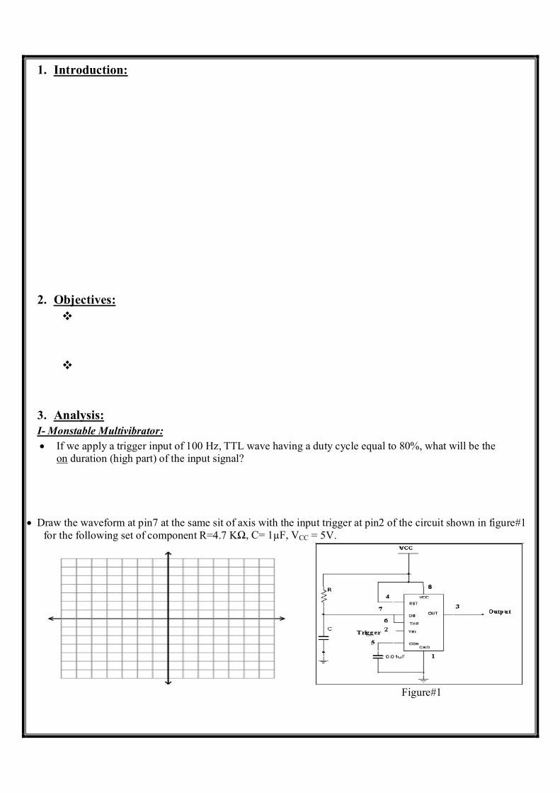
1. Introduction:
2. Objectives:
3. Analysis: I- Monstable Multivibrator: If we apply a trigger input of 100 Hz, TTL wave having a duty cycle equal to 80%, what will be the
on duration (high part) of the input signal?
Draw the waveform at pin7 at the same sit of axis with the input trigger at pin2 of the circuit shown in figure#1 for the following set of component R=4.7 KΩ, C= 1µF, VCC = 5V.
Figure#1
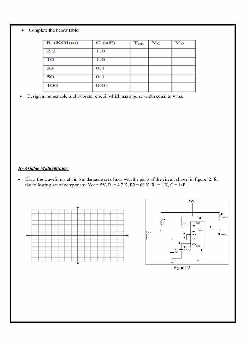
Complete the below table:
Design a monostable multivibrator circuit which has a pulse width equal to 4 ms.
II- Astable Multivibrator: Draw the waveforms at pin 6 at the same set of axis with the pin 3 of the circuit shown in figure#2, for
the following set of component: VCC = 5V, R1 = 4.7 K, R2 = 68 K, RL = 1 K, C = 1nF.
Figure#2
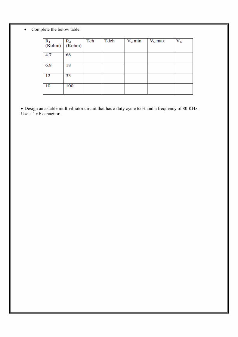
Complete the below table:
Design an astable multivibrator circuit that has a duty cycle 65% and a frequency of 80 KHz. Use a 1 nF capacitor.

4. Conclusion and discussion:
Facility of Engineering
Biomedical Engineering Department
Medical Electronic Lab
BME (317)
EXP#10: Schmitt Trigger Characteristics And Waveform Generation
Post-Report
Student Name:
Student Number:
Submission Date:
1. Introduction:
2. Objectives:
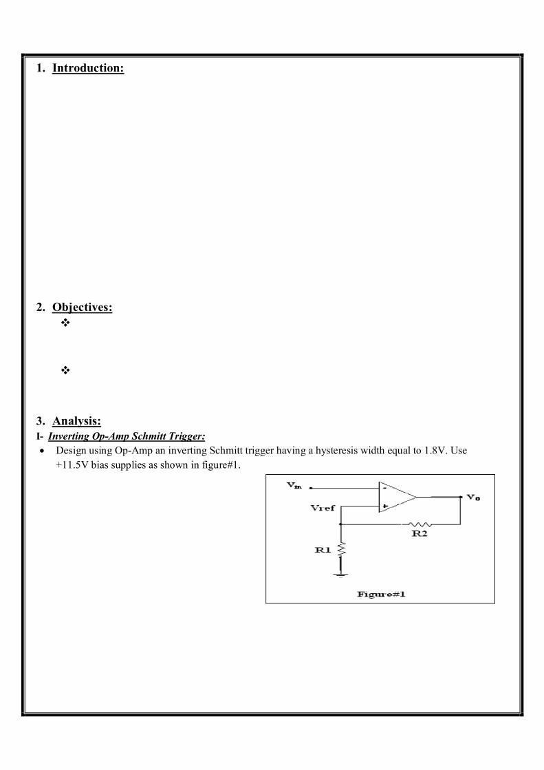
3. Analysis: I- Inverting Op-Amp Schmitt Trigger: Design using Op-Amp an inverting Schmitt trigger having a hysteresis width equal to 1.8V. Use
+11.5V bias supplies as shown in figure#1.
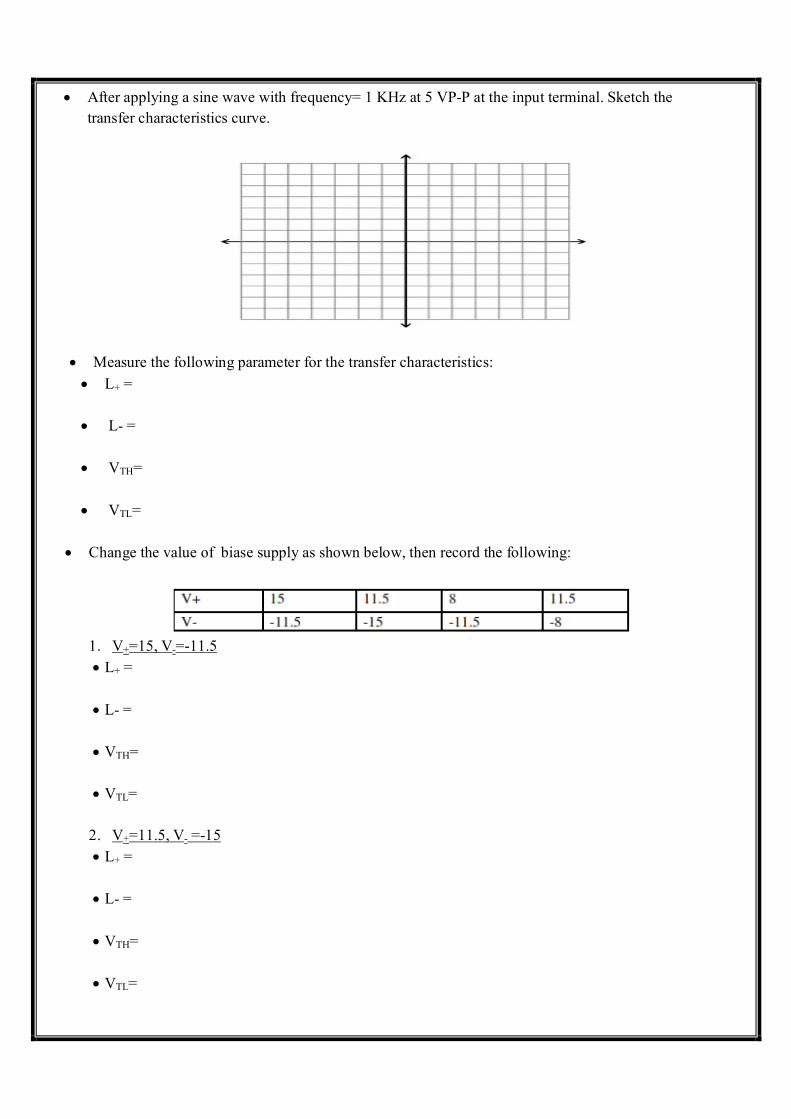
After applying a sine wave with frequency= 1 KHz at 5 VP-P at the input terminal. Sketch the transfer characteristics curve.
Measure the following parameter for the transfer characteristics: L+ =
L- =
VTH=
VTL=
Change the value of biase supply as shown below, then record the following:
1. V+=15, V-=-11.5 L+ =
L- =
VTH=
VTL=
2. V+=11.5, V- =-15 L+ =
L- =
VTH=
VTL=
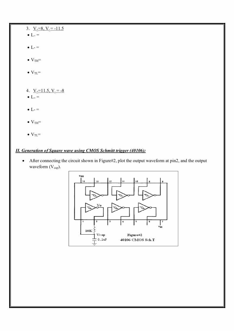
3. V+=8, V- = -11.5 L+ =
L- =
VTH=
VTL=
4. V+=11.5, V- = -8 L+ =
L- =
VTH=
VTL=
II. Generation of Square wave using CMOS Schmitt trigger (40106):
After connecting the circuit shown in Figure#2, plot the output waveform at pin2, and the output waveform (Vcap).
Output at pin (2) Output Vcap
Measure the following parameters: Tch=
Tdch=
Vcap =
Duty cycle=
L+=
L-=
VTH=
VTL=

4. Conclusion and discussion: