Embed Size (px)
Citation preview
Faculty of Engineering
Department of Biomedical Engineering
BME211
Circuit Analysis Laboratory Manual
Prepared by
BME EEE Dr. Özlem BİRGÜL Dr. Gökhan SOYSAL Dr. Görkem SAYGILI Dr. Deniz KARAÇOR
Gökhan GÜNEY Fatma Gül ALTUN Büşra ÖZGÖDE YİGİN Cansel FIÇICI
Contents
Introduction .................................................................................................................................................. 3
Laboratory Guidelines .................................................................................................................................. 3
Laboratory Safety ......................................................................................................................................... 4
Basic Laboratory Equipments ....................................................................................................................... 5
Experiment #1:
Part#1: Resistors in DC Circuits, Measurement of Voltage and Current, Ohm’s Law…………………………………10
Part#2: Kirchhoff’s Voltage and Current Laws, Equivalent Resistance, Resistive Voltage and Current
Dividers .…..……………………………………………………………………………………………………………………………………………17
Experiment #2: Superposition Principle, Power Calculations, Power Balancing ........................................ 19
Experiment #3: Thevenin and Norton Equivalent Circuits, Maximum Power Transfer ............................. 22
Experiment #4:
Part#1: Capacitors and Inductors, RC and RL Circuits……………………………………………………………..….……………27
Part#2: RC – RL Time Constants………………………………………………………………………………………………………………34
Experiment#5: RLC Circuits………………………………………………………………………………………………….…………………39
Experiment#6: Low-Pass and High-Pass Filters…………………………………………………………………………….…………44
Experiment#7: Resonance Circuits, Band-Pass and Band-Reject Filters……………………………………………….....49
APPENDIX A International System of Units ................................................................................................ 58
APPENDIX B Quick References for Devices................................................................................................. 60
3
Introduction This manual is prepared for an Electrical Circuits Laboratory Course which is taken simultanously with a
Circuit Analysis Course of a related Engineering Undergraduate Program. The manual starts with the
guidelines to be followed in the laboratory, introductory safety instructions and explanations for the basic
devices. Ten experiments for DC and AC electrical circuits cover the topics ranging from basic resistive
circuits, Ohm’s and Kirchhoff’s Laws, superposition theorem, power calculations and maximum power
transform, Thevenin’s Theorem, operational amplifiers, inductors and capacitors, first and second order
circuits and frequency selective circuits.
The equipments and components used in each experiment are listed at the end of each procedure and
are supplied by the department. Each station includes a digital oscilloscope, a signal generator, a DC power
supply and a desk-type multimeter. An electronic breadboard, which is a unit for building temporary
circuits, is required for all experiments. The students are encouraged to obtain and bring their own boards
for the experiments, yet, one will be provided to each station if needed. Similary, students can use their
own handheld digital multimeters if they prefer. Students are not allowed to swap equipments between
stations without approval of their assistants.
A set of appendices including useful informations that students may need during the experiments are
provided at the end of the manual. Appendix A gives a summary of the international system of units which
may be helpful in prepation of reports. In Appendix B, Quick Reference for Devices available in our own
laboratory are provided. Basic components (resistors, capacitor, etc.) available in the laboratory are listed
in Appendix C to guide the students in their design assigments.
Laboratory Guidelines
In this section specific guidelines for BME211 Electrical Circuits Laboratory class taken in the second year
of Ankara University Biomedical Engineering Undergraduate Program are given. The laboratory is
designed to be carried out consequently with BME201 Circuit Analysis Course. The content can be
summarized as:
- Introduction to the class, safety guidelines,
- 11 experiments, written midterm, experimental final
- Preliminary work
- Quiz
- Short summary by the assistant
- Procedure, Groups of two
- Report
- Performance
4
Laboratory Safety Safety is crucial in both our daily life and in laboratory work. We are responsible for creating safe working
environment for you in the laboratory and you yourself are responsible for your own safety by following
and maintaining safety precautions. Help ensure your safety when working around electricity and
electronic devices by learning to :
• Recognize and avoid potantial dangers.
• Pay attention to all warnings and cautions.
• Follow good personal and laboratory safety habits.
In this course, your chances of working with any equipment that could cause an electrically related
accident are as small as possible. Any work around electricity and electronic devices, however, can be
dangerous under certain conditions. Thus, you must be aware of what causes accidents and pay attention
to all warnings and cautions. You must also develop and follow good safety habits.
Save all practical jokes for outside the work area. Such behaviour has no place in laboratory or at work.
PREVENT ACCIDENTS: FOLLOW THESE ADVICES
• Never hurry. Work deliberately and carefully.
• Use appropriate safety equipment when required to do so.
• Check over all tools and equipment before using them. Report any defects or problems to your instructor.
• Connect to the power source LAST.
• If you are working with a lab kit that has internal power supplies, turn the main power switch OFF before you begin work on the circuits. Wait a few seconds for power supply capacitors to discharge. These steps will also help prevent damage to circuits.
• If you are working with a circuit that will be connected to an external power supply, turn the power switch of the external supply OFF before you begin to work on the circuit.
• Check the power supply voltages for proper value and for type (DC, AC, frequency) before connecting it to your circuit.
• Do not run wires over moving/rotating equipment, or on the floor, and do not string them across walkways from bench-to-bench.
• Remove conductive watch bands or chains, finger rings, wrist watches, etc., and do not use metallic pencils, metal or metal edge rulers, etc. when working with exposed circuits.
• When using large electrolytic capacitors be sure to wait long enough (approximately five time constants) for the capacitors to discharge before working on the circuit.
• All conducting surfaces intended to be at ground potential should be connected together.
• In case there is a smoke or over-heating on your circuit, or you think there is something wrong in
your experimental setup (laboratory equipments, circuit elements on your board, etc.), ask help
from your instructors. Do not touch any device on your circuit or on your desk.
5
Basic Laboratory Equipments
Multimeter
A digital multimeter (DMM) is a test tool used to measure electrical values. It is a standard diagnostic
tool in the electrical/electronic industries.
Measurements that can commonly be done using a multimeter are;
• Resistance
• Voltage
• Current
• Capacitance
• Frequency
• Temperature, etc.
Caution! Multimeters are connected serially to measure the current and in parallel to measure the
voltage. Before starting the measurement, checking the connections on the multimeter is highly
important to avoid burning the fuses and making the correct measuments.
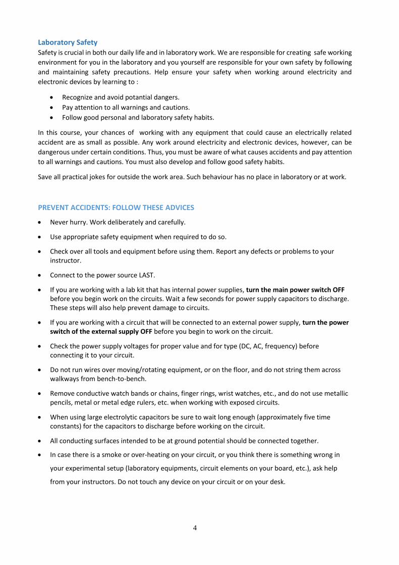
Waveforms and Function Generators Waveforms A waveform graphically represents a variable as a function of time. A DC (direct current) voltage or current
is a fixed value and does not vary with time. An AC (alternating current) voltage or current varies with
time.
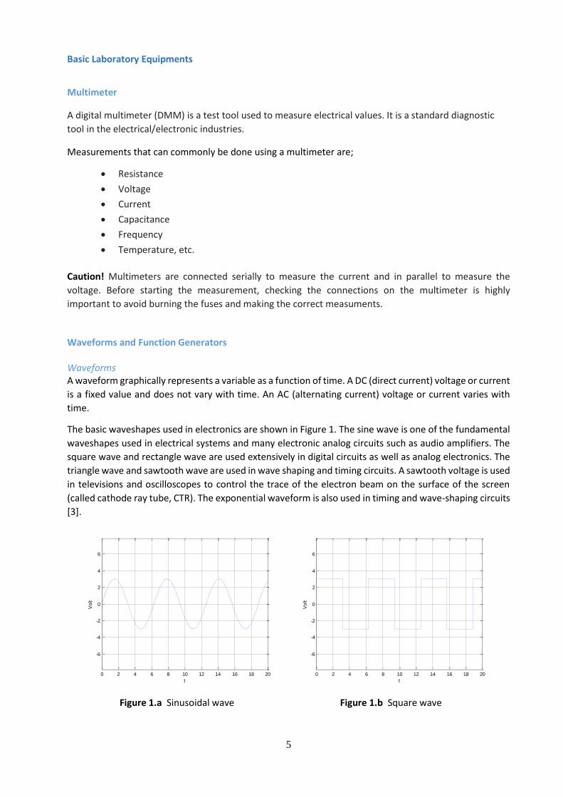
The basic waveshapes used in electronics are shown in Figure 1. The sine wave is one of the fundamental
waveshapes used in electrical systems and many electronic analog circuits such as audio amplifiers. The
square wave and rectangle wave are used extensively in digital circuits as well as analog electronics. The
triangle wave and sawtooth wave are used in wave shaping and timing circuits. A sawtooth voltage is used
in televisions and oscilloscopes to control the trace of the electron beam on the surface of the screen
(called cathode ray tube, CTR). The exponential waveform is also used in timing and wave-shaping circuits
[3].
Figure 1.a Sinusoidal wave Figure 1.b Square wave
0 2 4 6 8 10 12 14 16 18 20
-6
-4
-2
0
2
4
6
t
Volt
0 2 4 6 8 10 12 14 16 18 20
-6
-4
-2
0
2
4
6
t
Volt
6
Figure 1.c Triangle wave Figure 1.d Sawtooth wave
Figure 1.e Exponential wave
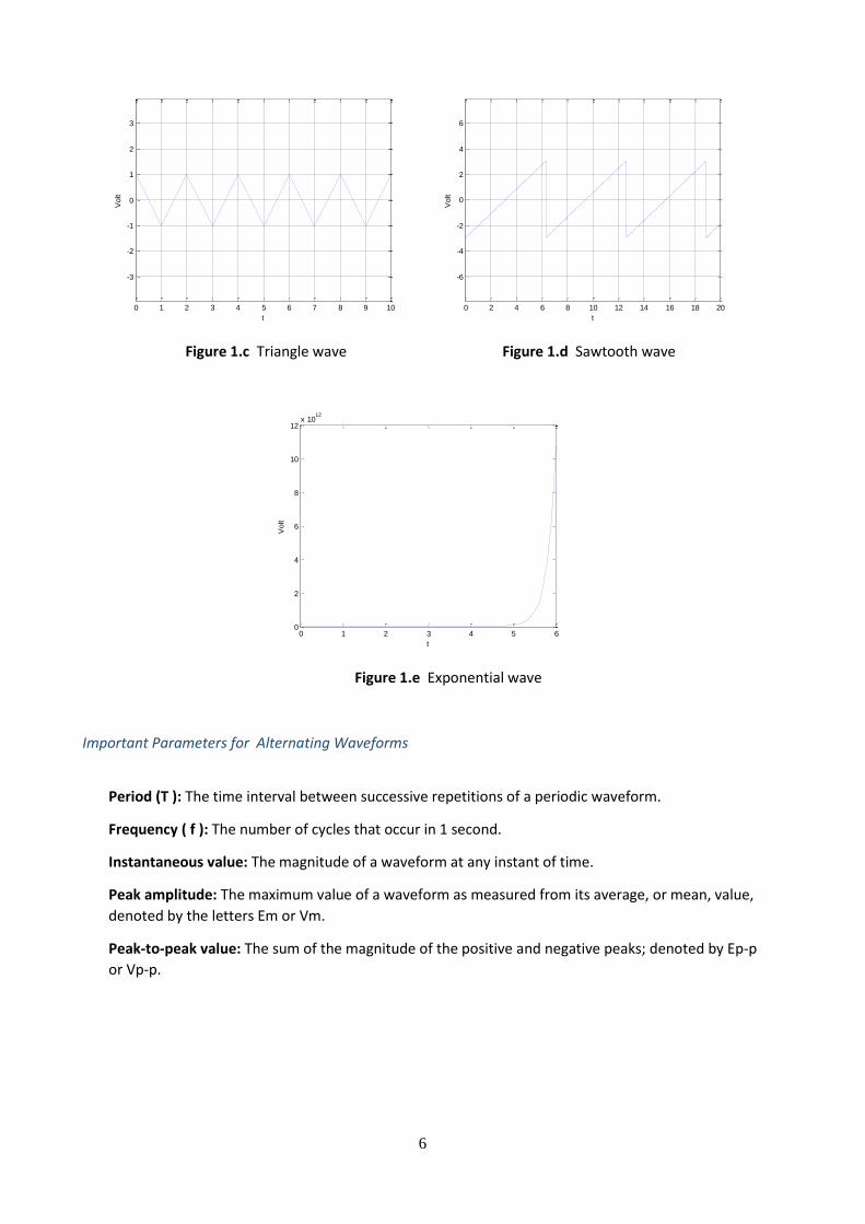
Important Parameters for Alternating Waveforms
Period (T ): The time interval between successive repetitions of a periodic waveform.
Frequency ( f ): The number of cycles that occur in 1 second.
Instantaneous value: The magnitude of a waveform at any instant of time.
Peak amplitude: The maximum value of a waveform as measured from its average, or mean, value,
denoted by the letters Em or Vm.
Peak-to-peak value: The sum of the magnitude of the positive and negative peaks; denoted by Ep-p
or Vp-p.
0 1 2 3 4 5 6 7 8 9 10
-3
-2
-1
0
1
2
3
t
Volt
0 2 4 6 8 10 12 14 16 18 20
-6
-4
-2
0
2
4
6
t
Volt
0 1 2 3 4 5 60
2
4
6
8
10
12x 10
12
t
Volt
7
Figure 2. Important parameters for a sinusoidal voltage
Phase Relationships
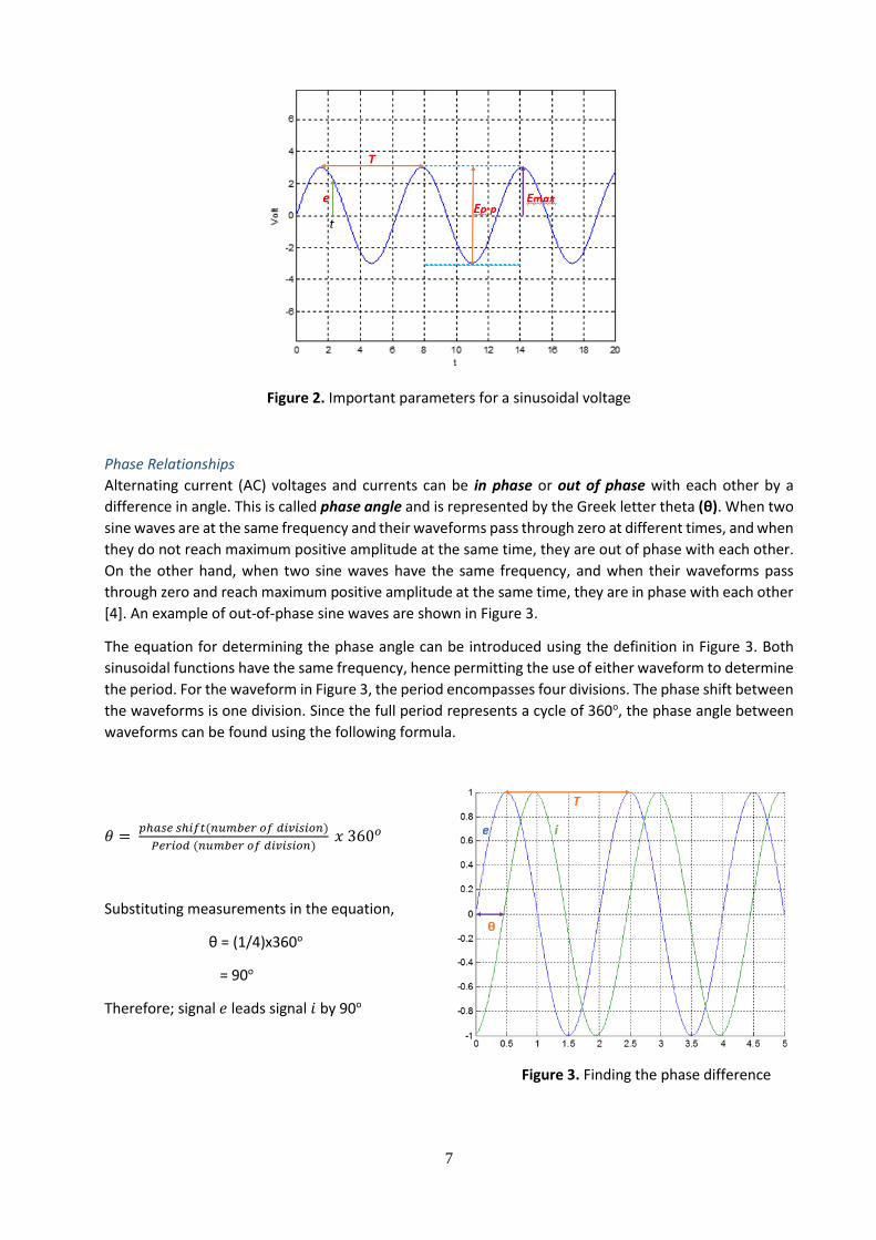
Alternating current (AC) voltages and currents can be in phase or out of phase with each other by a
difference in angle. This is called phase angle and is represented by the Greek letter theta (θ). When two
sine waves are at the same frequency and their waveforms pass through zero at different times, and when
they do not reach maximum positive amplitude at the same time, they are out of phase with each other.
On the other hand, when two sine waves have the same frequency, and when their waveforms pass
through zero and reach maximum positive amplitude at the same time, they are in phase with each other
[4]. An example of out-of-phase sine waves are shown in Figure 3.
The equation for determining the phase angle can be introduced using the definition in Figure 3. Both
sinusoidal functions have the same frequency, hence permitting the use of either waveform to determine
the period. For the waveform in Figure 3, the period encompasses four divisions. The phase shift between
the waveforms is one division. Since the full period represents a cycle of 360o, the phase angle between
waveforms can be found using the following formula.
𝜃 = 𝑝ℎ𝑎𝑠𝑒 𝑠ℎ𝑖𝑓𝑡(𝑛𝑢𝑚𝑏𝑒𝑟 𝑜𝑓 𝑑𝑖𝑣𝑖𝑠𝑖𝑜𝑛)
𝑃𝑒𝑟𝑖𝑜𝑑 (𝑛𝑢𝑚𝑏𝑒𝑟 𝑜𝑓 𝑑𝑖𝑣𝑖𝑠𝑖𝑜𝑛) 𝑥 360𝑜
Substituting measurements in the equation,
θ = (1/4)x360o
= 90o
Therefore; signal 𝑒 leads signal 𝑖 by 90o
Figure 3. Finding the phase difference
8
Effective (RMS) Value
The effective value of an AC signal is the value of a direct current which when applied to a given circuit for
a given time, produces the same expenditure of energy as produced by the alternating current when
flowing through the same circuit for the same period [5]. Effective value is also called the root-mean-
square (rms) value. This term comes from the mathematical method used to find its value [4]. The
effective value of any quantity plotted as a function of time can be found as
𝐼𝑒𝑓𝑓 = √∫ 𝑖2(𝑡)𝑑𝑡𝑇
0
𝑇
For the case of a pure sinusoidal waveform, the rms value equals to 1 √2⁄ or 0.707 times it peak value.
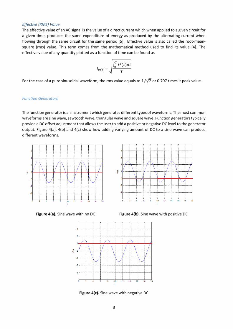
Function Generators
The function generator is an instrument which generates different types of waveforms. The most common
waveforms are sine wave, sawtooth wave, triangular wave and square wave. Function generators typically
provide a DC offset adjustment that allows the user to add a positive or negative DC level to the generator
output. Figure 4(a), 4(b) and 4(c) show how adding variying amount of DC to a sine wave can produce
different waveforms.
Figure 4(a). Sine wave with no DC Figure 4(b). Sine wave with positive DC
Figure 4(c). Sine wave with negative DC
9
Oscilloscope
The primary function of an oscilloscope is to display an exact replica of a voltage waveform as a function
of time. This picture of the waveform can be used to determine quantitive information such as the
amplitude and frequency of the waveforms as well as qualitive information such as the shape of the
waveform. The oscilloscope can also display more than one waveform at the same time for comparison.
and measure their time and phase relationships.
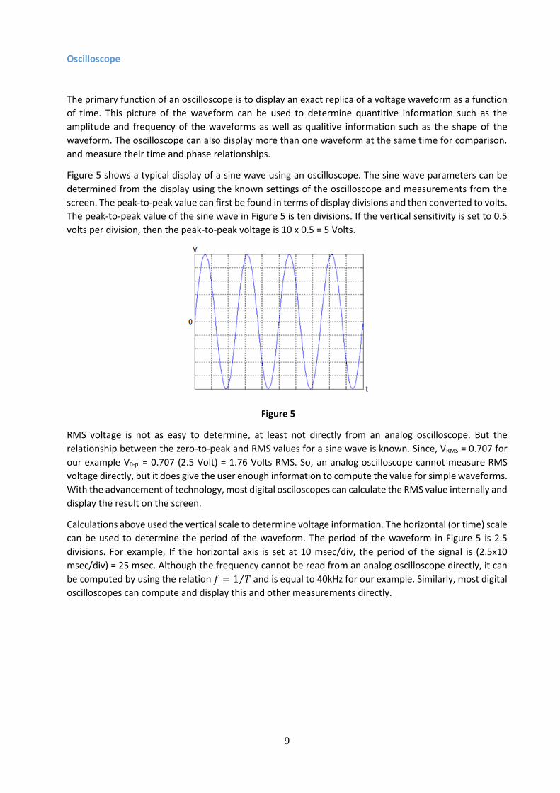
Figure 5 shows a typical display of a sine wave using an oscilloscope. The sine wave parameters can be
determined from the display using the known settings of the oscilloscope and measurements from the
screen. The peak-to-peak value can first be found in terms of display divisions and then converted to volts.
The peak-to-peak value of the sine wave in Figure 5 is ten divisions. If the vertical sensitivity is set to 0.5
volts per division, then the peak-to-peak voltage is 10 x 0.5 = 5 Volts.
Figure 5
RMS voltage is not as easy to determine, at least not directly from an analog oscilloscope. But the
relationship between the zero-to-peak and RMS values for a sine wave is known. Since, VRMS = 0.707 for
our example V0-p = 0.707 (2.5 Volt) = 1.76 Volts RMS. So, an analog oscilloscope cannot measure RMS
voltage directly, but it does give the user enough information to compute the value for simple waveforms.
With the advancement of technology, most digital osciloscopes can calculate the RMS value internally and
display the result on the screen.
Calculations above used the vertical scale to determine voltage information. The horizontal (or time) scale
can be used to determine the period of the waveform. The period of the waveform in Figure 5 is 2.5
divisions. For example, If the horizontal axis is set at 10 msec/div, the period of the signal is (2.5x10
msec/div) = 25 msec. Although the frequency cannot be read from an analog oscilloscope directly, it can
be computed by using the relation 𝑓 = 1 𝑇⁄ and is equal to 40kHz for our example. Similarly, most digital
oscilloscopes can compute and display this and other measurements directly.
10
Experiment #1
Part#1: Resistors in DC Circuits, Measurement of Voltage and Current, Ohm’s Law
Objective
The objective of this experiment is to become familiar with the concept of resistance, to learn resistor types and color coding, to measure DC voltage and current using digitial multimeters and to examine Ohm’s Law using different circuits.
Background
1. Resistors
The flow of charge through any material encounters an opposing force similar in many respects to mechanical friction. This opposition, due to the collisions between electrons and between electrons and other atoms in the material, which converts electrical energy into another form of energy such as heat, is called the resistance of the material. The circuit element used to model this behaviour is the resistor [1].
The unit of measurement of resistance is the ohm (Ω, the capital Greek letter omega). The circuit symbol and notation for resistance is given in Figure 1.1.
Figure 1.1 Resistance symbol and notation
Types of resistors
Resistors are made in many forms, but all belong in either of two groups: fixed or variable.
a) Fixed Resistors
Fixed resistors are classified into wire-wound resistors, composition resistors, and metal-film resistors:
Wire-Wound Resistors
Wire-wound resistors are made by winding wire of nickel-chromium alloy on a ceramic tube covering with a vitreous coating. The spiral winding has inductive and capacitive characteristics that make it suitable for operating above 50kHz. The frequency limit can be raised by noninductive winding so that the magnetic field produced by the two parts of the winding is cancelled [2].
Composition Resistors
Composition resistors are composed of carbon particles mixed with binder. This mixture is molded into a cylindirical shape and hardened by baking. Leads are attached axially to each end, and the assembly is encapsuled in a protective encapsulation coating. Color bands on the outer surface indicate the resistance value
Figure 1.2 Wire-Wound Resistor [2]
Figure 1.3 Composition Resistor [2]
11
and tolerance. Composition resistors are economical and exhibit low noise levels for resistance above 1MΩ. Composition resistors are usually rated for temperatures in the neighborhood of 70⁰C for power ranging from 1/8 to 2W. Composition resistors have end-to-end shunted capacitance that may be noticed at frequencies in the neighborhood of 100 kHz, especially for resistance values above 0.3 MΩ [2].
Metal-Film Resistors
Metal film resistors are commonly made of nichrome, tin-oxide or tantalum nitride, either hermetically sealed or using molded-phenolic cases. Metal-film resistors are not as stable as the wire-wound resistors [2].
b) Variable Resistors
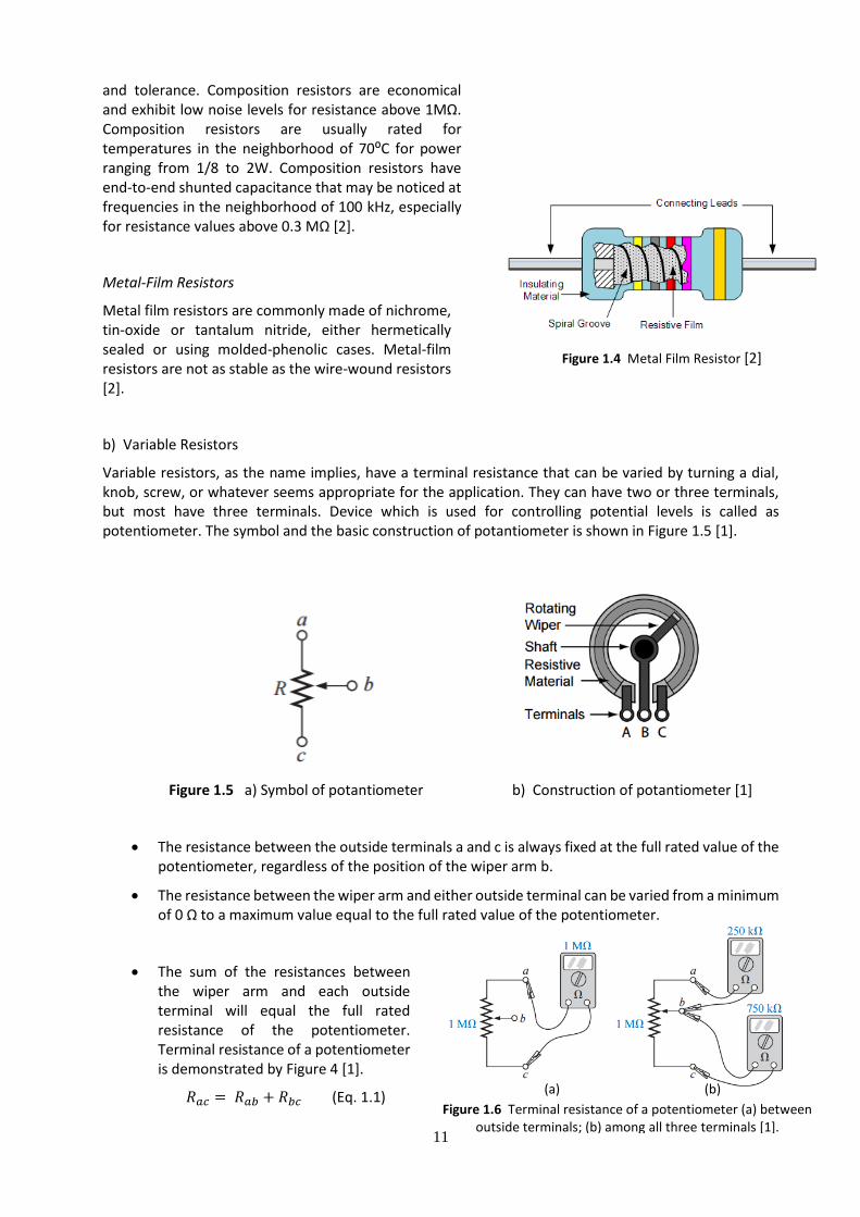
Variable resistors, as the name implies, have a terminal resistance that can be varied by turning a dial, knob, screw, or whatever seems appropriate for the application. They can have two or three terminals, but most have three terminals. Device which is used for controlling potential levels is called as potentiometer. The symbol and the basic construction of potantiometer is shown in Figure 1.5 [1].
Figure 1.5 a) Symbol of potantiometer b) Construction of potantiometer [1]
• The resistance between the outside terminals a and c is always fixed at the full rated value of the potentiometer, regardless of the position of the wiper arm b.
• The resistance between the wiper arm and either outside terminal can be varied from a minimum of 0 Ω to a maximum value equal to the full rated value of the potentiometer.
• The sum of the resistances between the wiper arm and each outside terminal will equal the full rated resistance of the potentiometer. Terminal resistance of a potentiometer is demonstrated by Figure 4 [1].
𝑅𝑎𝑐 = 𝑅𝑎𝑏 + 𝑅𝑏𝑐 (Eq. 1.1)
Figure 1.4 Metal Film Resistor [2]
Figure 1.6 Terminal resistance of a potentiometer (a) between outside terminals; (b) among all three terminals [1].
(a) (b)
12
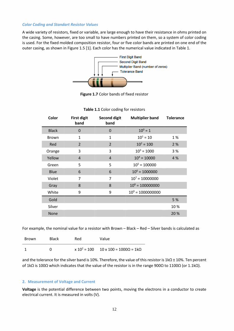
Color Coding and Standart Resistor Values
A wide variety of resistors, fixed or variable, are large enough to have their resistance in ohms printed on the casing. Some, however, are too small to have numbers printed on them, so a system of color coding is used. For the fixed molded composition resistor, four or five color bands are printed on one end of the outer casing, as shown in Figure 1.5 [1]. Each color has the numerical value indicated in Table 1.
Figure 1.7 Color bands of fixed resistor
Table 1.1 Color coding for resistors
Color First digit band
Second digit band
Multiplier band Tolerance
Black 0 0 100 = 1
Brown 1 1 101 = 10 1 %
Red 2 2 102 = 100 2 %
Orange 3 3 103 = 1000 3 %
Yellow 4 4 104 = 10000 4 %
Green 5 5 105 = 100000
Blue 6 6 106 = 1000000
Violet 7 7 107 = 10000000
Gray 8 8 108 = 100000000
White 9 9 109 = 1000000000
Gold 5 %
Silver 10 %
None 20 %
For example, the nominal value for a resistor with Brown – Black – Red – Silver bands is calculated as
Brown Black Red Value
1 0 x 102 = 100 10 x 100 = 1000Ω = 1kΩ
and the tolerance for the silver band is 10%. Therefore, the value of this resistor is 1kΩ ± 10%. Ten percent
of 1kΩ is 100Ω which indicates that the value of the resistor is in the range 900Ω to 1100Ω (or 1.1kΩ).
2. Measurement of Voltage and Current
Voltage is the potential difference between two points, moving the electrons in a conductor to create electrical current. It is measured in volts (V).
13
Current is described as the time rate of change of charge, measured in amperes (A). A direct current (DC) is a current that remains constant with time. An alternating current (AC) is a current that varies with time.
The assignment of the reference polarity for voltage and current are entirely arbitrary. However, once you have assigned the references, you must write all subsequent equations to agree with the chosen references. The most widely used sign convention is passive sign convention, which we use throughout our experiments. The passive sign convention can be stated as follows:
Whenever the reference direction for the current in an element is in the direction of the reference voltage drop across the element (as in Figure), use a positive sign in any expression that relates the voltage to the current. Otherwise, use negative sign [2].
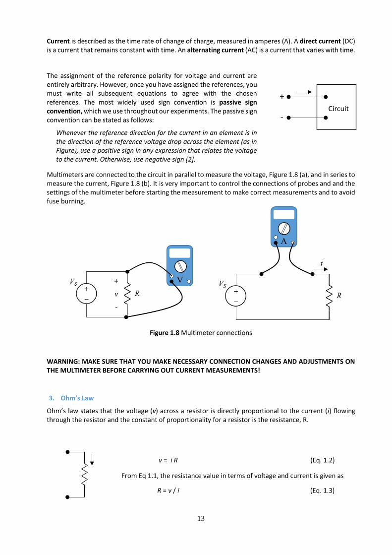
Multimeters are connected to the circuit in parallel to measure the voltage, Figure 1.8 (a), and in series to measure the current, Figure 1.8 (b). It is very important to control the connections of probes and and the settings of the multimeter before starting the measurement to make correct measurements and to avoid fuse burning.
Figure 1.8 Multimeter connections
WARNING: MAKE SURE THAT YOU MAKE NECESSARY CONNECTION CHANGES AND ADJUSTMENTS ON THE MULTIMETER BEFORE CARRYING OUT CURRENT MEASUREMENTS!
3. Ohm’s Law
Ohm’s law states that the voltage (v) across a resistor is directly proportional to the current (i) flowing through the resistor and the constant of proportionality for a resistor is the resistance, R.
v = i R (Eq. 1.2)
From Eq 1.1, the resistance value in terms of voltage and current is given as
R = v / i (Eq. 1.3)
+
-
Circuit
14
Part#2: Kirchhoff’s Voltage and Current Laws, Equivalent Resistance, Resistive Voltage and
Current Dividers Objective
The objective of this experiment is to examine Kirchoff’s Voltage Law and Kirchoff’s Current Law using simple resistive circuits. Voltage, current and equivalent resistance for different combinations of resistors and voltage and current divider rules are investigated.
Background
1. Kirchhoff’s Voltage Law
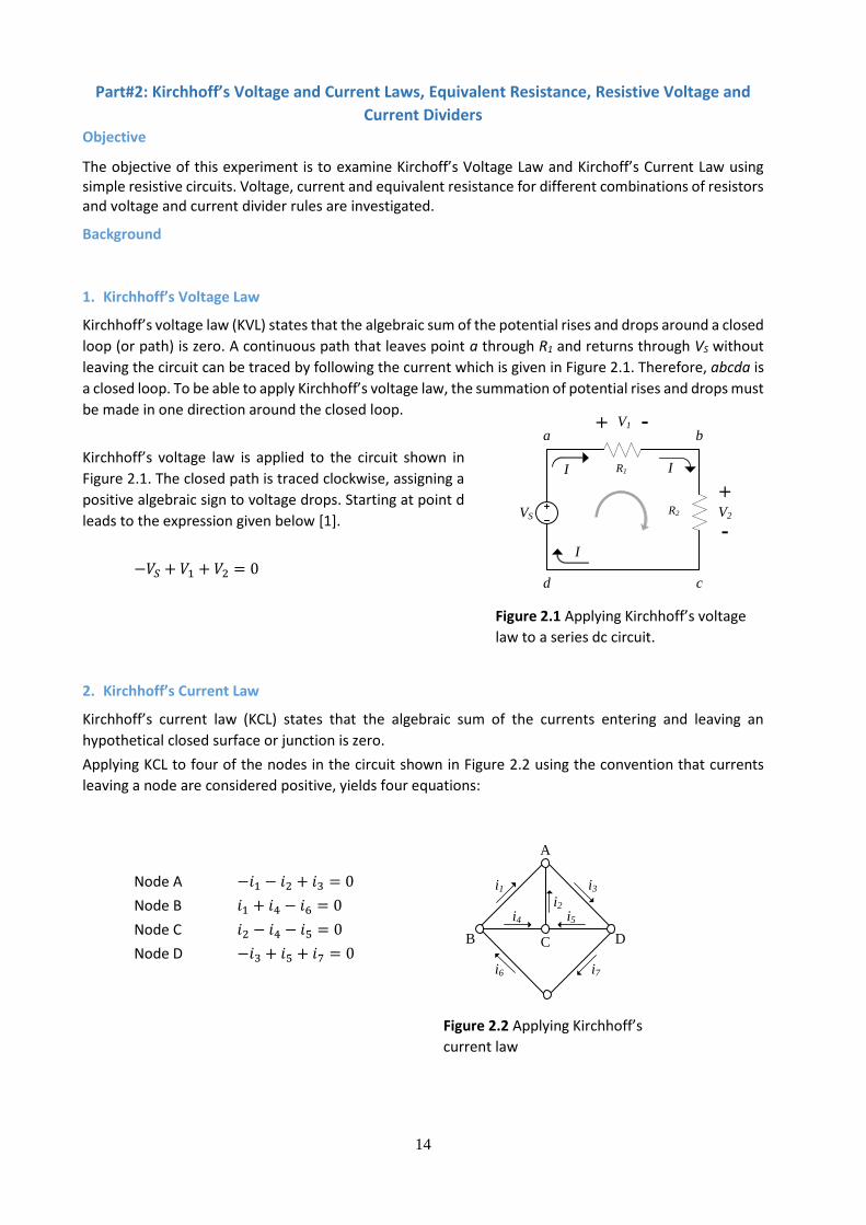
Kirchhoff’s voltage law (KVL) states that the algebraic sum of the potential rises and drops around a closed
loop (or path) is zero. A continuous path that leaves point a through R1 and returns through VS without
leaving the circuit can be traced by following the current which is given in Figure 2.1. Therefore, abcda is
a closed loop. To be able to apply Kirchhoff’s voltage law, the summation of potential rises and drops must
be made in one direction around the closed loop.
Kirchhoff’s voltage law is applied to the circuit shown in
Figure 2.1. The closed path is traced clockwise, assigning a
positive algebraic sign to voltage drops. Starting at point d
leads to the expression given below [1].
−𝑉𝑆 + 𝑉1 + 𝑉2 = 0
Figure 2.1 Applying Kirchhoff’s voltage
law to a series dc circuit.
2. Kirchhoff’s Current Law
Kirchhoff’s current law (KCL) states that the algebraic sum of the currents entering and leaving an
hypothetical closed surface or junction is zero.
Applying KCL to four of the nodes in the circuit shown in Figure 2.2 using the convention that currents
leaving a node are considered positive, yields four equations:
Node A −𝑖1 − 𝑖2 + 𝑖3 = 0
Node B 𝑖1 + 𝑖4 − 𝑖6 = 0
Node C 𝑖2 − 𝑖4 − 𝑖5 = 0
Node D −𝑖3 + 𝑖5 + 𝑖7 = 0
Figure 2.2 Applying Kirchhoff’s
current law
VS
V1
V2
R1
R2
a b
cd
I
I
I
+ -
+
-
i1
i2
i3
i4 i5
i6 i7
A
B C D
15
VSR2
Io
R1
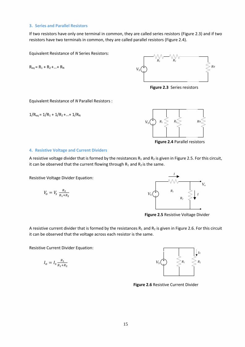
3. Series and Parallel Resistors
If two resistors have only one terminal in common, they are called series resistors (Figure 2.3) and if two
resistors have two terminals in common, they are called parallel resistors (Figure 2.4).
Equivalent Resistance of N Series Resistors:
Req = R1 + R2 +…+ RN
Figure 2.3 Series resistors
Equivalent Resistance of N Parallel Resistors :
1/Req = 1/R1 + 1/R2 +…+ 1/RN
Figure 2.4 Parallel resistors
4. Resistive Voltage and Current Dividers
A resistive voltage divider that is formed by the resistances R1 and R2 is given in Figure 2.5. For this circuit,
it can be observed that the current flowing through R1 and R2 is the same.
Resistive Voltage Divider Equation:
𝑉𝑜 = 𝑉𝑠 𝑅2
𝑅1+𝑅2
Figure 2.5 Resistive Voltage Divider
A resistive current divider that is formed by the resistances R1 and R2 is given in Figure 2.6. For this circuit
it can be observed that the voltage across each resistor is the same.
Resistive Current Divider Equation:
𝐼𝑜 = 𝐼𝑠𝑅1
𝑅1+𝑅2
Figure 2.6 Resistive Current Divider
VS
R1 R2
RN
R1 R2 RNVS
VS
R1
R2
I
Vo
I
16
VS
R1 R2
R3
Preliminary Work
1. Find magnitude ranges for resistors with the following color bands:
a. Blue – Grey – Red – Gold
b. Red – Violet– Black – Silver
c. Red – Violet– Brown – Gold
2. Calculate the desired voltage or current values for the following cases using Ohm’s Law:
a. Calculate the current through the 1.5 kΩ resistor, if the voltage drop on the resistor is 15 V.
b. Calculate the current through the 750 Ω, 6.8k Ω and 100k Ω resistors respectively, if the voltage drop on each of them is 15 V.
c. Calculate the current through the 6.8 kΩ resistor, if the voltage drops on the resistor are 5 V, 10 V and 15 V respectively.
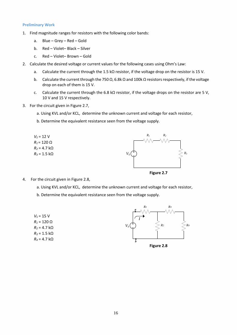
3. For the circuit given in Figure 2.7,
a. Using KVL and/or KCL, determine the unknown current and voltage for each resistor,
b. Determine the equivalent resistance seen from the voltage supply.
VS = 12 V
R1 = 120 Ω
R2 = 4.7 kΩ
R3 = 1.5 kΩ
Figure 2.7
4. For the circuit given in Figure 2.8,
a. Using KVL and/or KCL, determine the unknown current and voltage for each resistor,
b. Determine the equivalent resistance seen from the voltage supply.
VS = 15 V
R1 = 120 Ω
R2 = 4.7 kΩ
R3 = 1.5 kΩ
R4 = 4.7 kΩ
Figure 2.8
VS
R1 R3
R2 R4
I
a
b
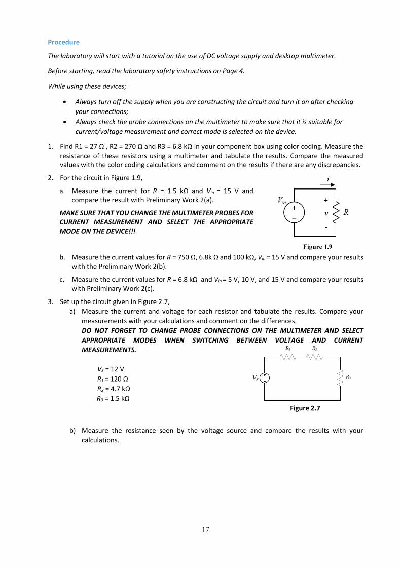
17
VS
R1 R2
R3
Procedure
The laboratory will start with a tutorial on the use of DC voltage supply and desktop multimeter.
Before starting, read the laboratory safety instructions on Page 4.
While using these devices;
• Always turn off the supply when you are constructing the circuit and turn it on after checking
your connections;
• Always check the probe connections on the multimeter to make sure that it is suitable for
current/voltage measurement and correct mode is selected on the device.
1. Find R1 = 27 Ω , R2 = 270 Ω and R3 = 6.8 kΩ in your component box using color coding. Measure the resistance of these resistors using a multimeter and tabulate the results. Compare the measured values with the color coding calculations and comment on the results if there are any discrepancies.
2. For the circuit in Figure 1.9,
a. Measure the current for R = 1.5 kΩ and Vin = 15 V and compare the result with Preliminary Work 2(a).
MAKE SURE THAT YOU CHANGE THE MULTIMETER PROBES FOR CURRENT MEASUREMENT AND SELECT THE APPROPRIATE MODE ON THE DEVICE!!!
b. Measure the current values for R = 750 Ω, 6.8k Ω and 100 kΩ, Vin = 15 V and compare your results with the Preliminary Work 2(b).
c. Measure the current values for R = 6.8 kΩ and Vin = 5 V, 10 V, and 15 V and compare your results with Preliminary Work 2(c).
3. Set up the circuit given in Figure 2.7,
a) Measure the current and voltage for each resistor and tabulate the results. Compare your
measurements with your calculations and comment on the differences.
DO NOT FORGET TO CHANGE PROBE CONNECTIONS ON THE MULTIMETER AND SELECT
APPROPRIATE MODES WHEN SWITCHING BETWEEN VOLTAGE AND CURRENT
MEASUREMENTS.
VS = 12 V
R1 = 120 Ω
R2 = 4.7 kΩ
R3 = 1.5 kΩ
Figure 2.7
b) Measure the resistance seen by the voltage source and compare the results with your
calculations.
Figure 1.9
18
4. Set up the circuit given in Figure 2.8,
a) Measure the current and voltage for each resistor and tabulate the results. Compare your
measurements with your calculations and comment on the differences.
VS = 15 V
R1 = 120 Ω
R2 = 4.7 kΩ
R3 = 1.5 kΩ
R4 = 4.7 kΩ
Figure 2.8
b) Measure the resistance seen by the voltage source and compare the results with your
calculations.
5. Using the 10 kΩ potantiometer in your component box:
a. Measure and record the resistance between the two outer terminals of the potantiometer. Does the reading change when you adjust the rotating wiper?
b. Adjust the rotating wiper of the potantiometer about midway between the two extremes. Measure and record the resistance between the central and one of the outer terminals of the potantiometer. Does the reading change when you adjust the rotating wiper?
c. Set the rotating wiper somewhere in between extreme values and record the resistance values between each outer terminal and central terminal. Calculate the sum of two values and compare it with your measurement in part (a). Comment on your results.
References
[1] Boylestad, Introductory Circuit Analysis (Tenth Edition)
[2] James W. Nilsson, Susan A. Riedel (Sixth Edition)
List of Components
Equipments: DC Voltage Supply, Digital Multimeter
Resistors: 27 Ω, 120 Ω, 270 Ω, 750 Ω, 1.5 kΩ, 4.7 kΩ, 6.8kΩ, 100 kΩ, 10 KΩ potantiometer
VS
R1 R3
R2 R4
I
a
b
19
Experiment #2
Superposition Principle, Power Calculations, Power Balancing
Objective
The objective of this experiment is to understand and apply the superposition principle on simple resistive circuits for circuit analysis. Power calculation for voltage supplies and resistors and balancing the total power in a circuit will also be investigated.
Background
1. Superposition
If a circuit has two or more independent sources, one way to determine the value of a specific variable
(voltage or current) is to use node-voltage or mesh-current method. Another way is to determine the
contribution of each independent source to the variable and then add them up. This approach is known
as the superposition. The idea of superposition relies on the linearity property. The superposition principle
states that the voltage across (or current through) an element in a linear circuit is the algebraic sum of the
voltages across (or currents through) that element due to each independent source acting alone [1].
Steps to apply superposition principle:
a) Turn off all independent sources except one source. Find the output (voltage or current).
b) Repeat step (a) for every other independent sources.
c) Find the total contribution by adding algebraically all the contributions due to the independent
sources. [1].
2. Power and Power Calculation
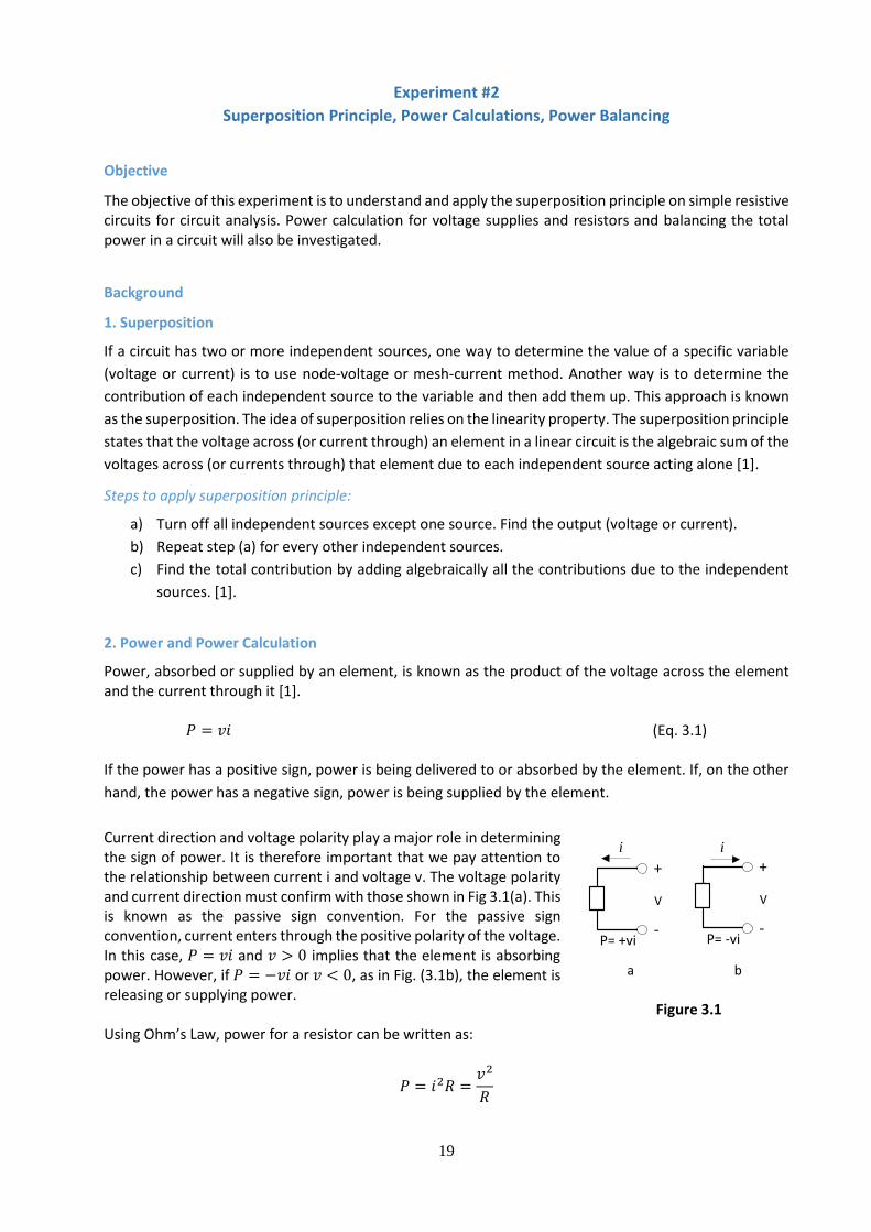
Power, absorbed or supplied by an element, is known as the product of the voltage across the element and the current through it [1].
𝑃 = 𝑣𝑖 (Eq. 3.1) If the power has a positive sign, power is being delivered to or absorbed by the element. If, on the other
hand, the power has a negative sign, power is being supplied by the element.
Current direction and voltage polarity play a major role in determining the sign of power. It is therefore important that we pay attention to the relationship between current i and voltage v. The voltage polarity and current direction must confirm with those shown in Fig 3.1(a). This is known as the passive sign convention. For the passive sign convention, current enters through the positive polarity of the voltage. In this case, 𝑃 = 𝑣𝑖 and 𝑣 > 0 implies that the element is absorbing power. However, if 𝑃 = −𝑣𝑖 or 𝑣 < 0, as in Fig. (3.1b), the element is releasing or supplying power. Using Ohm’s Law, power for a resistor can be written as:
𝑃 = 𝑖2𝑅 =𝑣2
𝑅
a b
+
-
V
P= +vi
i
+
-
V
P= -vi
i
Figure 3.1
20
3. Power Balancing
Before starting power balancing we have to understand law of conservation of power. Law of conversation of energy states that, in a closed system, i.e., a system that is isolated from its surroundings, the total energy of the system is conserved. This law must be satisfied in any electric circuit. For this reason, the algebraic sum of power in a circuit, at any instant of time, must be zero:
∑ 𝑃 = 0 This again confirms the fact that the total power supplied to the circuit must balance the total power absorbed. Preliminary Work
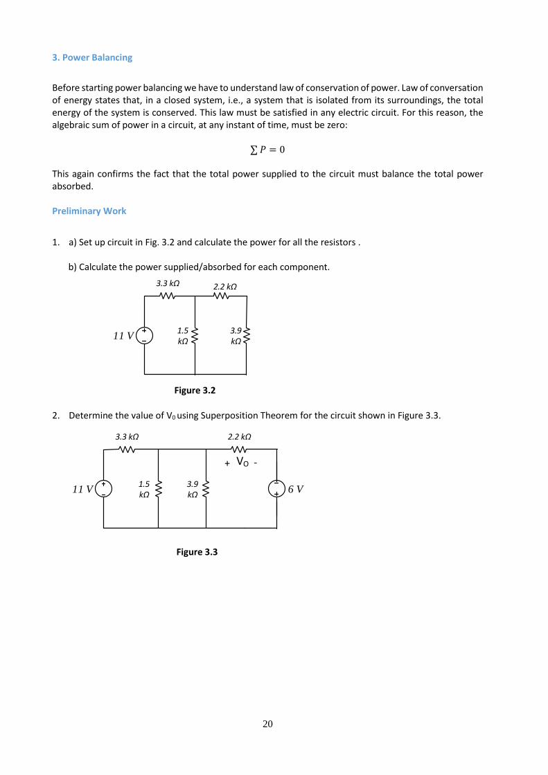
1. a) Set up circuit in Fig. 3.2 and calculate the power for all the resistors . b) Calculate the power supplied/absorbed for each component.
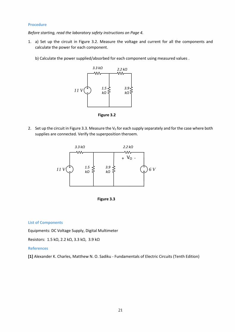
2. Determine the value of V0 using Superposition Theorem for the circuit shown in Figure 3.3.
11 V
3.3 kΩ 2.2 kΩ
1.5 kΩ
3.9 kΩ
6 V
+ -VO
11 V
3.3 kΩ 2.2 kΩ
1.5 kΩ
3.9 kΩ
Figure 3.2
Figure 3.3
21
Procedure
Before starting, read the laboratory safety instructions on Page 4.
1. a) Set up the circuit in Figure 3.2. Measure the voltage and current for all the components and
calculate the power for each component.
b) Calculate the power supplied/absorbed for each component using measured values .
Figure 3.2
2. Set up the circuit in Figure 3.3. Measure the V0 for each supply separately and for the case where both
supplies are connected. Verify the superposition theroem.
List of Components
Equipments: DC Voltage Supply, Digital Multimeter
Resistors: 1.5 kΩ, 2.2 kΩ, 3.3 kΩ, 3.9 kΩ
References
[1] Alexander K. Charles, Matthew N. O. Sadiku - Fundamentals of Electric Circuits (Tenth Edition)
11 V
3.3 kΩ 2.2 kΩ
1.5 kΩ
3.9 kΩ
11 V
3.3 kΩ 2.2 kΩ
1.5 kΩ
3.9 kΩ
6 V
+ -VO
Figure 3.3
22
Experiment #3
Thevenin and Norton Equivalent Circuits, Maximum Power Transfer Objective
The objective of this experiment to learn equivalent circuits, determine and utilize Thevenin and Norton equivalent circuits, understand the concept of maximum power transfer and find components to achieve maximum power transfer.
Background
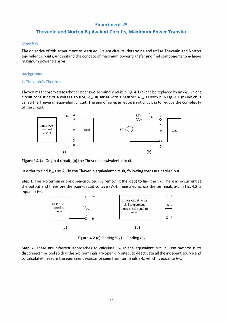
1. Thevenin’s Theorem Thevenin’s theorem states that a linear two-terminal circuit in Fig. 4.1 (a) can be replaced by an equivalent circuit consisting of a voltage source, VTh, in series with a resistor, RTh, as shown in Fig. 4.1 (b) which is called the Thevenin equivalent circuit. The aim of using an equivalent circuit is to reduce the complexity of the circuit.
(a) (b)
Figure 4.1 (a) Original circuit, (b) the Thevenin equivalent circuit. In order to find VTh and RTh in the Thevenin equivalent circuit, following steps are carried out: Step 1: The a-b terminals are open-circuited (by removing the load) to find the VTh. There is no current at the output and therefore the open-circuit voltage (VOC), measured across the terminals a-b in Fig. 4.2 is equal to VTh.
(a) (b)
Figure 4.2 (a) Finding VTh (b) Finding RTh
Step 2: There are different approaches to calculate RTh in the equivalent circuit. One method is to disconnect the load so that the a-b terminals are open-circuited; to deactivate all the indepent source and to calculate/measure the equivalent resistance seen from terminals a-b, which is equal to RTh.
Linear two-
terminal
circuit
Ia
b
+
-
V Load Load
a
b
IRTh
+
V
-
VTh
Linear two-
terminal
circuit
+
-
VOC
a
b
Linear circuit with
all independent
sources set equal to
zero
+
-
a
b
Rin
23
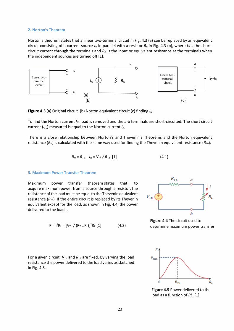
2. Norton’s Theorem Norton’s theorem states that a linear two-terminal circuit in Fig. 4.3 (a) can be replaced by an equivalent circuit consisting of a current source IN in parallel with a resistor RN in Fig. 4.3 (b), where IN is the short-circuit current through the terminals and RN is the input or equivalent resistance at the terminals when the independent sources are turned off [1].
(a) (b) (c) Figure 4.3 (a) Original circuit (b) Norton equivalent circuit (c) finding IN To find the Norton current IN, load is removed and the a-b terminals are short-circuited. The short circuit current (ISC) measured is equal to the Norton current IN.
There is a close relationship between Norton’s and Thevenin’s Theorems and the Norton equivalent resistance (RN) is calculated with the same way used for finding the Thevenin equivalent resistance (RTh).
RN = RTh, IN = VTh / RTh [1] (4.1)
3. Maximum Power Transfer Theorem Maximum power transfer theorem states that, to acquire maximum power from a source through a resistor, the resistance of the load must be equal to the Thevenin equivalent resistance (RTh). If the entire circuit is replaced by its Thevenin equivalent except for the load, as shown in Fig. 4.4, the power delivered to the load is
P = i2RL = [VTh / (RTh+ RL)]2RL
[1] (4.2) For a given circuit, VTh and RTh are fixed. By varying the load resistance the power delivered to the load varies as sketched in Fig. 4.5.
Linear two-
terminal
circuit
+
-
a
b
b
a
IN RN
Linear two-
terminal
circuit
+
-
a
b
İSC=IN
Figure 4.5 Power delivered to the load as a function of RL. [1]
Figure 4.4 The circuit used to
determine maximum power transfer
24
12 V
a
b
2.7 kΩ 4.7 kΩ
1.5 kΩ
3.9 kΩ
3 A
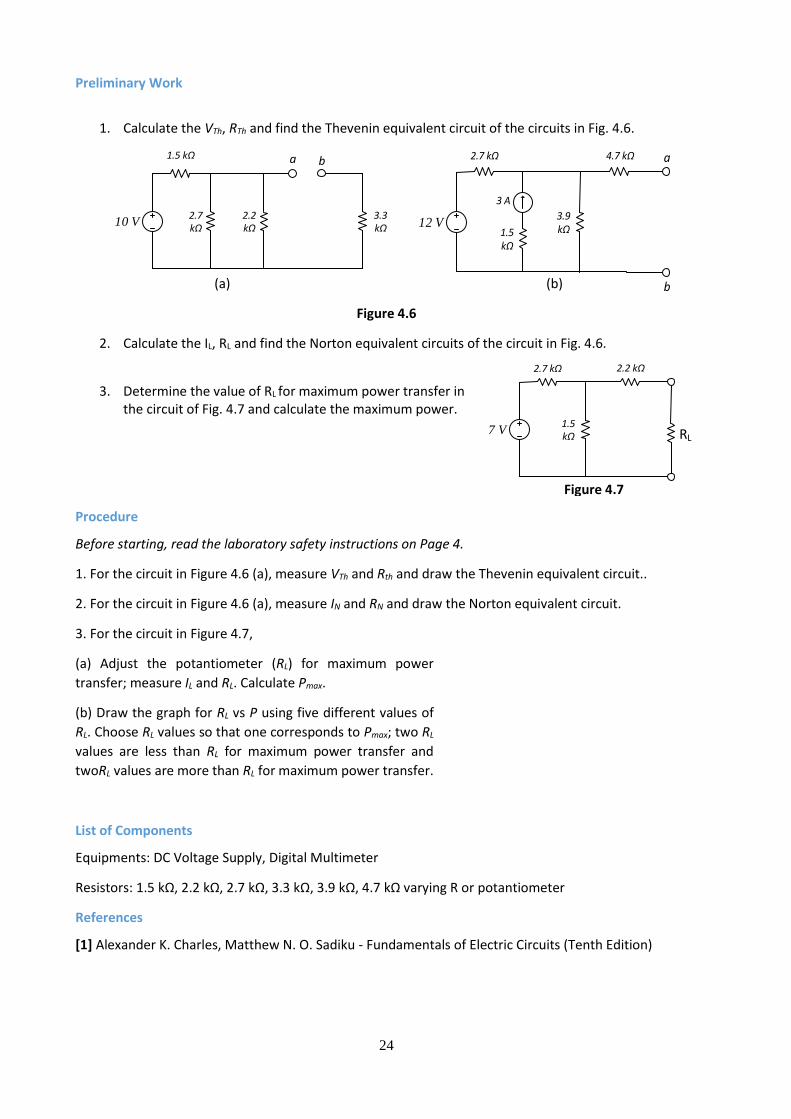
Preliminary Work
1. Calculate the VTh, RTh and find the Thevenin equivalent circuit of the circuits in Fig. 4.6.
(a) (b)
Figure 4.6
2. Calculate the IL, RL and find the Norton equivalent circuits of the circuit in Fig. 4.6.
3. Determine the value of RL for maximum power transfer in the circuit of Fig. 4.7 and calculate the maximum power.
Procedure
Before starting, read the laboratory safety instructions on Page 4.
1. For the circuit in Figure 4.6 (a), measure VTh and Rth and draw the Thevenin equivalent circuit..
2. For the circuit in Figure 4.6 (a), measure IN and RN and draw the Norton equivalent circuit.
3. For the circuit in Figure 4.7,
(a) Adjust the potantiometer (RL) for maximum power
transfer; measure IL and RL. Calculate Pmax.
(b) Draw the graph for RL vs P using five different values of
RL. Choose RL values so that one corresponds to Pmax; two RL
values are less than RL for maximum power transfer and
twoRL values are more than RL for maximum power transfer.
List of Components
Equipments: DC Voltage Supply, Digital Multimeter
Resistors: 1.5 kΩ, 2.2 kΩ, 2.7 kΩ, 3.3 kΩ, 3.9 kΩ, 4.7 kΩ varying R or potantiometer
References
[1] Alexander K. Charles, Matthew N. O. Sadiku - Fundamentals of Electric Circuits (Tenth Edition)
10 V
1.5 kΩ b
2.7 kΩ
2.2 kΩ
a
3.3 kΩ
7 V
2.7 kΩ 2.2 kΩ
1.5 kΩ RL
Figure 4.7
25
Experiment #4
Part#1: Capacitors and Inductors, RC and RL Circuits
Objective
The objective of this experiment is to understand and analyze circuits that contains capacitors or inductors
which are components that can store energy. The relation between terminal voltage and terminal current
for these components and first order circuits that are composed of resistors and either capacitors or
inductors will be studied. The consept of phasors will be introduced and applied to first order circuits.
Background
1. Capacitors
The capacitor is one of the three basic passive circuit components (resistor, capacitor, inductor) of any
electronic or electrical circuit. Resistance in a circuit gives rise to ohmic or watt losses, and its current is
in phase with the applied voltage waveform. Inductance or a capacitance gives rise to currents out of
phase with voltage by 90o in AC circuits, and is the cause of transient currents in many circuits. A capacitor
works in electric field. It stores energy when a steady voltage is applied. It gets charged to the applied
voltage and keeps the energy as well as the voltage even after removal of external voltage. This factor
makes handling of capacitors quite dangerous at times, and caution must be exercised when working with
them. A capacitor offers an open circuit to the flow of DC current in steady state. Current in ideal capacitor
leads the voltage by 90o in AC circuits [3].
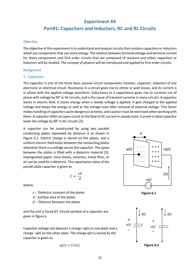
A capacitor can be constructed by using two parallel
conducting plates separated by distance d as shown in
Figure 6.1. Electric charge is stored on the plates, and a
uniform electric field exists between the conducting plates
whenever there is a voltage across the capacitor. The space
between the plates is filled with a dielectric material [5].
Impregnated paper, mica sheets, ceramics, metal films, or
air can be used for a dielectric. The capacitance value of the
paralel plate capacitor is given as
𝐶 = 𝜀𝐴
𝑑
where;
𝜀 ∶ Dielectric constant of the plates
𝐴 ∶ Surface area of the plates
𝑑 ∶ Distance between the plates
and the unit is Farad (F). Circuit symbols of a capacitor are
given in figure x.
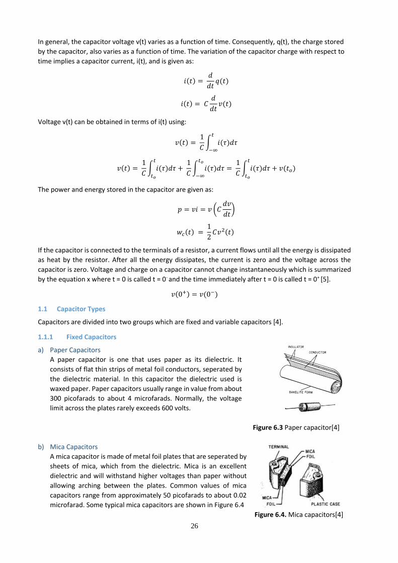
Capacitor voltage v(t) deposits a charge +q(t) on one plate and a
charge –q(t) on the other plate. The charge q(t) is stored by the
capacitor is given as.
𝑞(𝑡) = 𝐶𝑣(𝑡)
v(t)
- - -- - -- - -- - -
+ + ++ + + + + + + + +
+q(t)-q(t)
d
i(t)
CC
i(t) i(t)
+
-
+
-
v(t)v(t)
Figure 6.1
Figure 6.2
26
In general, the capacitor voltage v(t) varies as a function of time. Consequently, q(t), the charge stored
by the capacitor, also varies as a function of time. The variation of the capacitor charge with respect to
time implies a capacitor current, i(t), and is given as:
𝑖(𝑡) = 𝑑
𝑑𝑡𝑞(𝑡)
𝑖(𝑡) = 𝐶𝑑
𝑑𝑡𝑣(𝑡)
Voltage v(t) can be obtained in terms of i(t) using:
𝑣(𝑡) = 1
𝐶∫ 𝑖(𝜏)𝑑𝜏
𝑡
−∞
𝑣(𝑡) = 1
𝐶∫ 𝑖(𝜏)𝑑𝜏
𝑡
𝑡𝑜
+ 1
𝐶∫ 𝑖(𝜏)𝑑𝜏
𝑡𝑜
−∞
= 1
𝐶∫ 𝑖(𝜏)𝑑𝜏
𝑡
𝑡𝑜
+ 𝑣(𝑡𝑜)
The power and energy stored in the capacitor are given as:
𝑝 = 𝑣𝑖 = 𝑣 (𝐶𝑑𝑣
𝑑𝑡)
𝑤𝑐(𝑡) = 1
2𝐶𝑣2(𝑡)
If the capacitor is connected to the terminals of a resistor, a current flows until all the energy is dissipated
as heat by the resistor. After all the energy dissipates, the current is zero and the voltage across the
capacitor is zero. Voltage and charge on a capacitor cannot change instantaneously which is summarized
by the equation x where t = 0 is called t = 0- and the time immediately after t = 0 is called t = 0+ [5].
𝑣(0+) = 𝑣(0−)
1.1 Capacitor Types
Capacitors are divided into two groups which are fixed and variable capacitors [4].
1.1.1 Fixed Capacitors
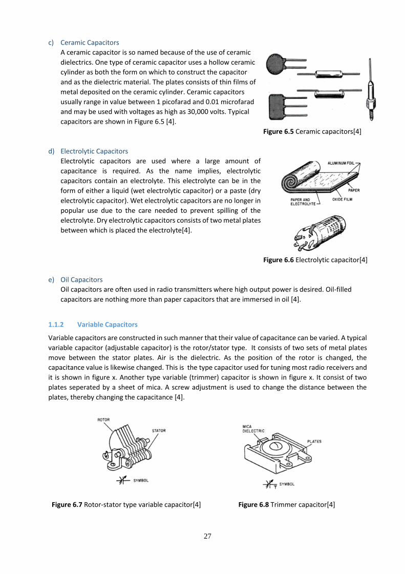
a) Paper Capacitors
A paper capacitor is one that uses paper as its dielectric. It
consists of flat thin strips of metal foil conductors, seperated by
the dielectric material. In this capacitor the dielectric used is
waxed paper. Paper capacitors usually range in value from about
300 picofarads to about 4 microfarads. Normally, the voltage
limit across the plates rarely exceeds 600 volts.
Figure 6.3 Paper capacitor[4]
b) Mica Capacitors
A mica capacitor is made of metal foil plates that are seperated by
sheets of mica, which from the dielectric. Mica is an excellent
dielectric and will withstand higher voltages than paper without
allowing arching between the plates. Common values of mica
capacitors range from approximately 50 picofarads to about 0.02
microfarad. Some typical mica capacitors are shown in Figure 6.4
Figure 6.4. Mica capacitors[4]
27
c) Ceramic Capacitors
A ceramic capacitor is so named because of the use of ceramic
dielectrics. One type of ceramic capacitor uses a hollow ceramic
cylinder as both the form on which to construct the capacitor
and as the dielectric material. The plates consists of thin films of
metal deposited on the ceramic cylinder. Ceramic capacitors
usually range in value between 1 picofarad and 0.01 microfarad
and may be used with voltages as high as 30,000 volts. Typical
capacitors are shown in Figure 6.5 [4].
Figure 6.5 Ceramic capacitors[4]
d) Electrolytic Capacitors
Electrolytic capacitors are used where a large amount of
capacitance is required. As the name implies, electrolytic
capacitors contain an electrolyte. This electrolyte can be in the
form of either a liquid (wet electrolytic capacitor) or a paste (dry
electrolytic capacitor). Wet electrolytic capacitors are no longer in
popular use due to the care needed to prevent spilling of the
electrolyte. Dry electrolytic capacitors consists of two metal plates
between which is placed the electrolyte[4].
Figure 6.6 Electrolytic capacitor[4]
e) Oil Capacitors
Oil capacitors are often used in radio transmitters where high output power is desired. Oil-filled
capacitors are nothing more than paper capacitors that are immersed in oil [4].
1.1.2 Variable Capacitors
Variable capacitors are constructed in such manner that their value of capacitance can be varied. A typical
variable capacitor (adjustable capacitor) is the rotor/stator type. It consists of two sets of metal plates
move between the stator plates. Air is the dielectric. As the position of the rotor is changed, the
capacitance value is likewise changed. This is the type capacitor used for tuning most radio receivers and
it is shown in figure x. Another type variable (trimmer) capacitor is shown in figure x. It consist of two
plates seperated by a sheet of mica. A screw adjustment is used to change the distance between the
plates, thereby changing the capacitance [4].
Figure 6.7 Rotor-stator type variable capacitor[4] Figure 6.8 Trimmer capacitor[4]
28
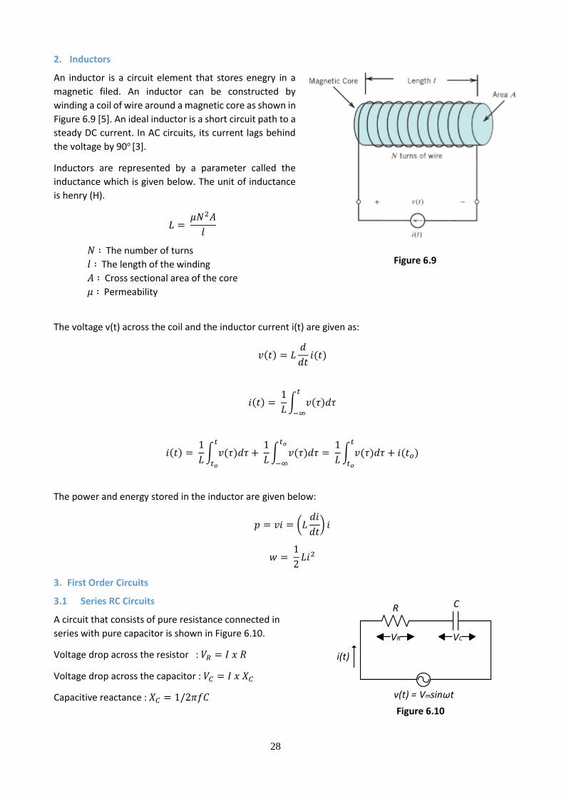
2. Inductors
An inductor is a circuit element that stores enegry in a
magnetic filed. An inductor can be constructed by
winding a coil of wire around a magnetic core as shown in
Figure 6.9 [5]. An ideal inductor is a short circuit path to a
steady DC current. In AC circuits, its current lags behind
the voltage by 90o [3].
Inductors are represented by a parameter called the
inductance which is given below. The unit of inductance
is henry (H).
𝐿 = 𝜇𝑁2𝐴
𝑙
𝑁 ∶ The number of turns
𝑙 ∶ The length of the winding
𝐴 ∶ Cross sectional area of the core
𝜇 ∶ Permeability
The voltage v(t) across the coil and the inductor current i(t) are given as:
𝑣(𝑡) = 𝐿𝑑
𝑑𝑡𝑖(𝑡)
𝑖(𝑡) = 1
𝐿∫ 𝑣(𝜏)𝑑𝜏
𝑡
−∞
𝑖(𝑡) = 1
𝐿∫ 𝑣(𝜏)𝑑𝜏
𝑡
𝑡𝑜
+ 1
𝐿∫ 𝑣(𝜏)𝑑𝜏
𝑡𝑜
−∞
= 1
𝐿∫ 𝑣(𝜏)𝑑𝜏
𝑡
𝑡𝑜
+ 𝑖(𝑡𝑜)
The power and energy stored in the inductor are given below:
𝑝 = 𝑣𝑖 = (𝐿𝑑𝑖
𝑑𝑡) 𝑖
𝑤 = 1
2𝐿𝑖2
3. First Order Circuits
3.1 Series RC Circuits
A circuit that consists of pure resistance connected in
series with pure capacitor is shown in Figure 6.10.
Voltage drop across the resistor : 𝑉𝑅 = 𝐼 𝑥 𝑅
Voltage drop across the capacitor : 𝑉𝐶 = 𝐼 𝑥 𝑋𝐶
Capacitive reactance : 𝑋𝐶 = 1/2𝜋𝑓𝐶
Figure 6.9
R C
v(t) = Vmsinωt
VR VC
i(t)
Figure 6.10
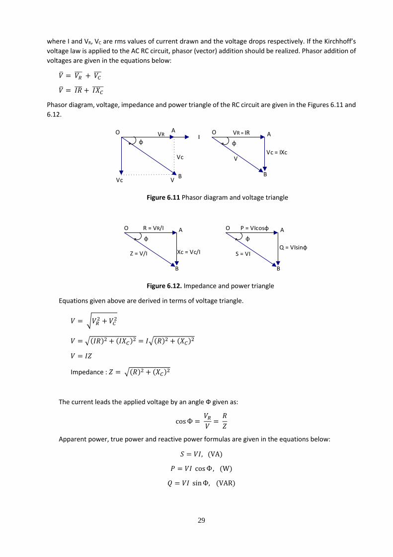
29
where I and VR, VC are rms values of current drawn and the voltage drops respectively. If the Kirchhoff’s
voltage law is applied to the AC RC circuit, phasor (vector) addition should be realized. Phasor addition of
voltages are given in the equations below:
= 𝑉𝑅 + 𝑉𝐶
= 𝐼𝑅 + 𝐼𝑋𝐶
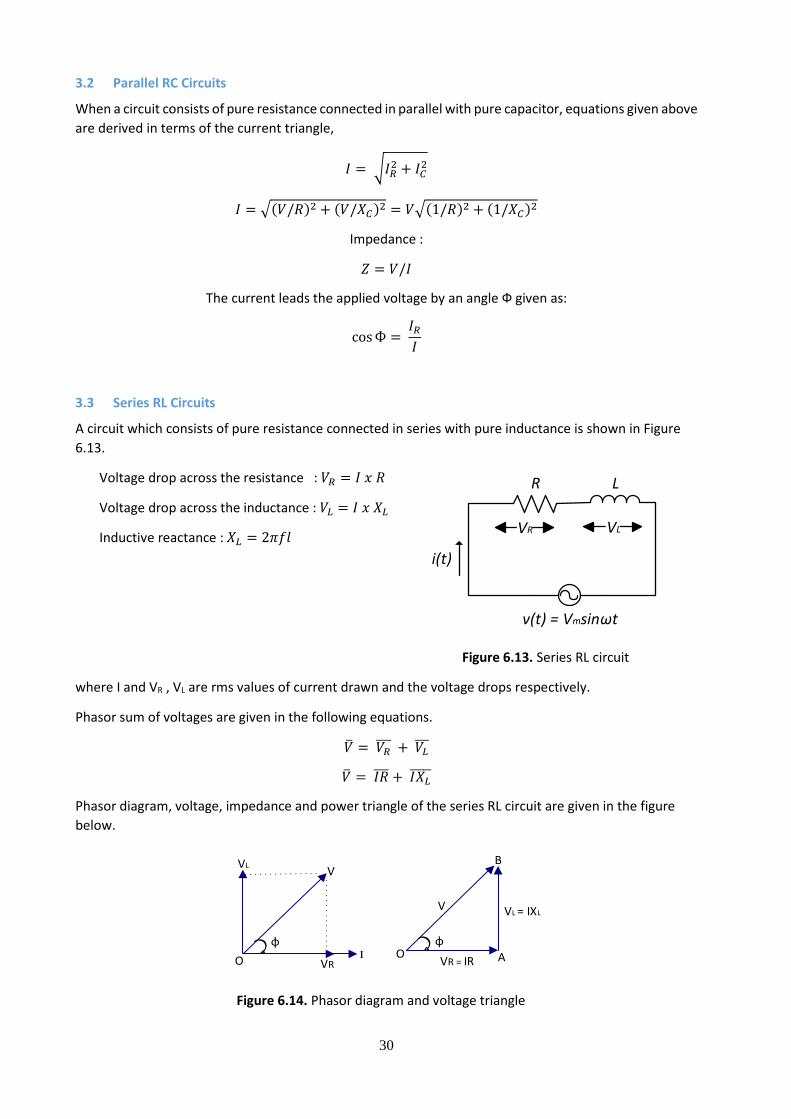
Phasor diagram, voltage, impedance and power triangle of the RC circuit are given in the Figures 6.11 and
6.12.
I
A
B
O
ɸ
Vc V
Vc
VR O A
B
VVc = IXc
VR = IR
ɸ
Figure 6.11 Phasor diagram and voltage triangle
Xc = Vc/I
R = VR/IO A
B
Z = V/I
ɸ
P = VIcosɸ O A
B
ɸ
Q = VIsinɸ S = VI
Figure 6.12. Impedance and power triangle
Equations given above are derived in terms of voltage triangle.
𝑉 = √𝑉𝑅2 + 𝑉𝐶
2
𝑉 = √(𝐼𝑅)2 + (𝐼𝑋𝐶)2 = 𝐼√(𝑅)2 + (𝑋𝐶)2
𝑉 = 𝐼𝑍
Impedance : 𝑍 = √(𝑅)2 + (𝑋𝐶)2
The current leads the applied voltage by an angle Ф given as:
cos Ф = 𝑉𝑅
𝑉=
𝑅
𝑍
Apparent power, true power and reactive power formulas are given in the equations below:
𝑆 = 𝑉𝐼, (VA)
𝑃 = 𝑉𝐼 cos Ф, (W)
𝑄 = 𝑉𝐼 sin Ф, (VAR)
30
3.2 Parallel RC Circuits
When a circuit consists of pure resistance connected in parallel with pure capacitor, equations given above
are derived in terms of the current triangle,
𝐼 = √𝐼𝑅2 + 𝐼𝐶
2
𝐼 = √(𝑉/𝑅)2 + (𝑉/𝑋𝐶)2 = 𝑉√(1/𝑅)2 + (1/𝑋𝐶)2
Impedance :
𝑍 = 𝑉/𝐼
The current leads the applied voltage by an angle Ф given as:
cos Ф = 𝐼𝑅
𝐼
3.3 Series RL Circuits
A circuit which consists of pure resistance connected in series with pure inductance is shown in Figure
6.13.
Voltage drop across the resistance : 𝑉𝑅 = 𝐼 𝑥 𝑅
Voltage drop across the inductance : 𝑉𝐿 = 𝐼 𝑥 𝑋𝐿
Inductive reactance : 𝑋𝐿 = 2𝜋𝑓𝑙
Figure 6.13. Series RL circuit
where I and VR , VL are rms values of current drawn and the voltage drops respectively.
Phasor sum of voltages are given in the following equations.
= 𝑉𝑅 + 𝑉𝐿
= 𝐼𝑅 + 𝐼𝑋𝐿
Phasor diagram, voltage, impedance and power triangle of the series RL circuit are given in the figure
below.
OI
VR
VVL
ɸ ɸ
VR = IR
VL = IXLV
O A
B
Figure 6.14. Phasor diagram and voltage triangle
R
v(t) = Vmsinωt
VR VL
i(t)
L
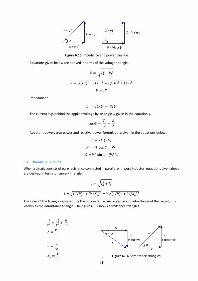
31
ɸ
R = VR/I
XL = VL/IZ = V/I
ɸ
P = VIcosɸ
S = VI Q = VIsinɸ
Figure 6.15 Impedance and power triangle
Equations given below are derived in terms of the voltage triangle.
𝑉 = √𝑉𝑅2 + 𝑉𝐿
2
𝑉 = √(𝐼𝑅)2 + (𝐼𝑋𝐿)2 = 𝐼√(𝑅)2 + (𝑋𝐿)2
𝑉 = 𝐼𝑍
Impedance :
𝑍 = √(𝑅)2 + (𝑋𝐿)2
The current lags behind the applied voltage by an angle Ф given in the equation x.
cos Ф = 𝑉𝑅
𝑉=
𝑅
𝑍
Apparent power, true power and reactive power formulas are given in the equations below.
𝑆 = 𝑉𝐼 (VA)
𝑃 = 𝑉𝐼 cos Ф (W)
𝑄 = 𝑉𝐼 sin Ф (VAR)
3.4 Parallel RL Circuits
When a circuit consists of pure resistance connected in parallel with pure inductor, equations given above
are derived in terms of current triangle,
𝐼 = √𝐼𝑅2 + 𝐼𝐿
2
𝐼 = √(𝑉/𝑅)2 + (𝑉/𝑋𝐿)2 = 𝑉√(1/𝑅)2 + (1/𝑋𝐿)2
The sides of the triangle representing the conductance, susceptance and admittance of the circuit, it is
known as the admittance triangle. The figure 6.16 shows admittance triangles.
𝐼2
𝑉2 = 𝐼𝑅
2
𝑉2 + 𝐼𝐿
2
𝑉2
𝑍 = 𝑉
𝐼
𝑅 = 𝑉
𝐼𝑅
𝑋𝐿 = 𝑉
𝐼𝐿 Figure 6.16 Admittance triangles
ɸ
Y
G
BC
capacitive
ɸ
G
Y
BL
inductive
32
Admittance : 𝑌 = 1
𝑍
Conductance : 𝐺 = 1
𝑅
Susteptance : 𝐵 =1
𝑋𝐿
𝑌2 = 𝐺2 + 𝐵2
The current lags behind the applied voltage by an angle Ф given as:
cos Ф = 𝐼𝑅
𝐼
Part#2: RC – RL Time Constants
Objective
The objective of this experiment is to understand the concept of time constants in simple series R-C and
series R-L circuits; observe the charging and discharging of a capacitor and compare the time constant
values for different capacitance and resistance values.
Background
RC Time Constants
Consider the first order RC circuit given in Figure 7.1
Figure 7.1 Series R-C circuit
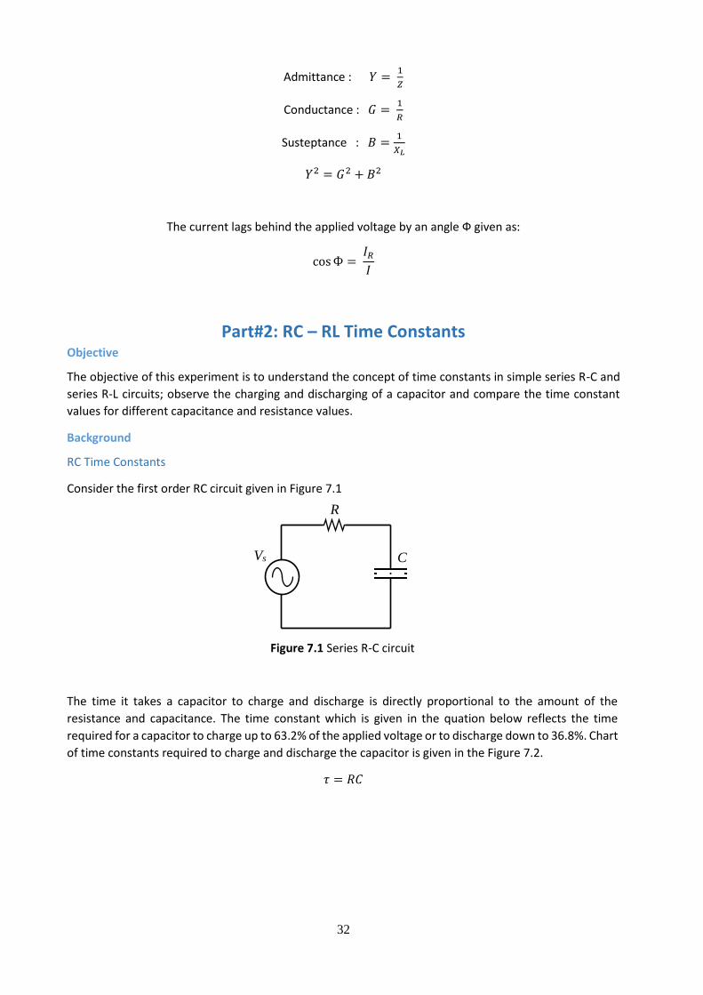
The time it takes a capacitor to charge and discharge is directly proportional to the amount of the
resistance and capacitance. The time constant which is given in the quation below reflects the time
required for a capacitor to charge up to 63.2% of the applied voltage or to discharge down to 36.8%. Chart
of time constants required to charge and discharge the capacitor is given in the Figure 7.2.
𝜏 = 𝑅𝐶
R
C Vs
33
Figure 7.2. Chart of time constants for capacitor
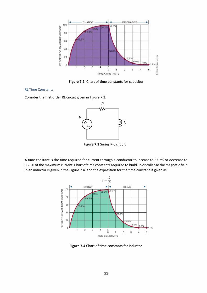
RL Time Constant:
Consider the first order RL circuit given in Figure 7.3.
Figure 7.3 Series R-L circuit
A time constant is the time required for current through a conductor to incease to 63.2% or decrease to
36.8% of the maximum current. Chart of time constants required to build up or collapse the magnetic field
in an inductor is given in the Figure 7.4 and the expression for the time constant is given as:
𝜏 =𝐿
𝑅
Figure 7.4 Chart of time constants for inductor
R
L
Vs
34
Preliminary Work
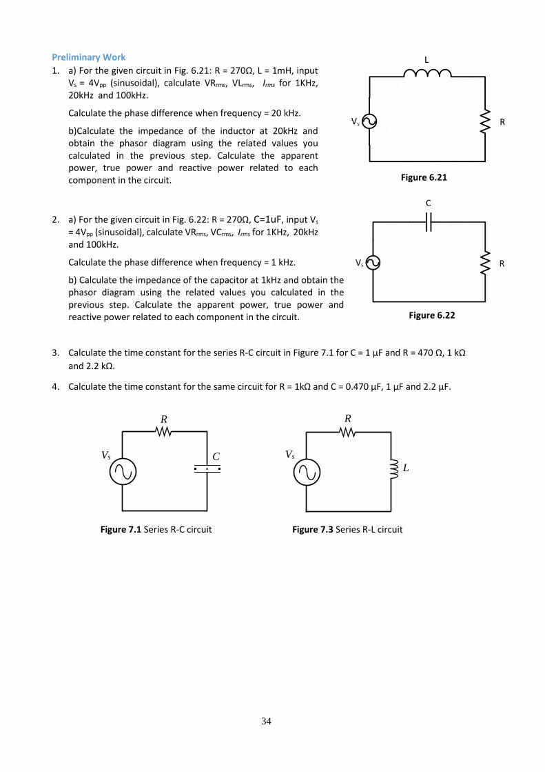
1. a) For the given circuit in Fig. 6.21: R = 270Ω, L = 1mH, input Vs = 4Vpp (sinusoidal), calculate VRrms, VLrms, Irms for 1KHz, 20kHz and 100kHz.
Calculate the phase difference when frequency = 20 kHz.
b)Calculate the impedance of the inductor at 20kHz and obtain the phasor diagram using the related values you calculated in the previous step. Calculate the apparent power, true power and reactive power related to each component in the circuit.
2. a) For the given circuit in Fig. 6.22: R = 270Ω, C=1uF, input Vs
= 4Vpp (sinusoidal), calculate VRrms, VCrms, Irms for 1KHz, 20kHz and 100kHz.
Calculate the phase difference when frequency = 1 kHz.
b) Calculate the impedance of the capacitor at 1kHz and obtain the phasor diagram using the related values you calculated in the previous step. Calculate the apparent power, true power and reactive power related to each component in the circuit.
3. Calculate the time constant for the series R-C circuit in Figure 7.1 for C = 1 µF and R = 470 Ω, 1 kΩ
and 2.2 kΩ.
4. Calculate the time constant for the same circuit for R = 1kΩ and C = 0.470 µF, 1 µF and 2.2 µF.
Figure 7.1 Series R-C circuit Figure 7.3 Series R-L circuit
Figure 6.21
Figure 6.22
R
C Vs
R
L
Vs
Figure 6.21
35
Procedure
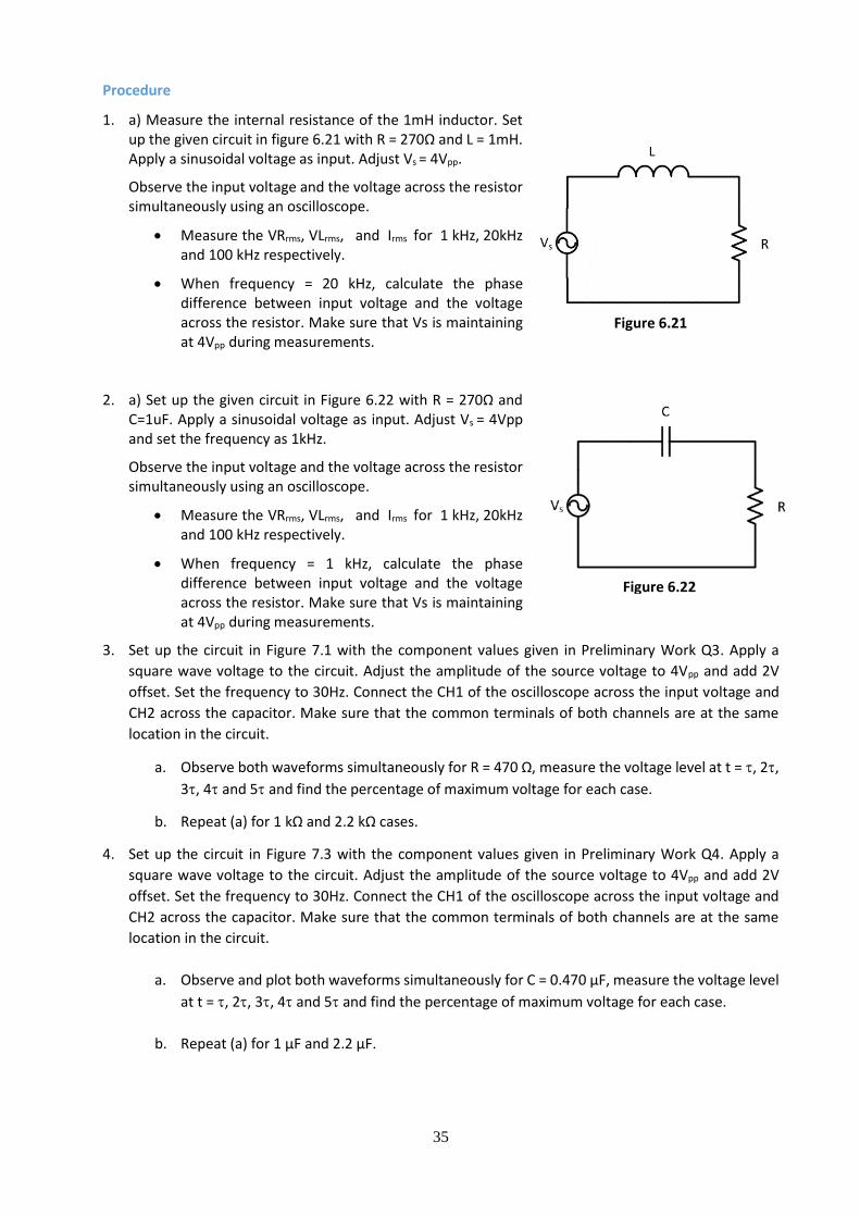
1. a) Measure the internal resistance of the 1mH inductor. Set up the given circuit in figure 6.21 with R = 270Ω and L = 1mH. Apply a sinusoidal voltage as input. Adjust Vs = 4Vpp.
Observe the input voltage and the voltage across the resistor simultaneously using an oscilloscope.
• Measure the VRrms, VLrms, and Irms for 1 kHz, 20kHz and 100 kHz respectively.
• When frequency = 20 kHz, calculate the phase difference between input voltage and the voltage across the resistor. Make sure that Vs is maintaining at 4Vpp during measurements.
2. a) Set up the given circuit in Figure 6.22 with R = 270Ω and C=1uF. Apply a sinusoidal voltage as input. Adjust Vs = 4Vpp and set the frequency as 1kHz.
Observe the input voltage and the voltage across the resistor simultaneously using an oscilloscope.
• Measure the VRrms, VLrms, and Irms for 1 kHz, 20kHz and 100 kHz respectively.
• When frequency = 1 kHz, calculate the phase difference between input voltage and the voltage across the resistor. Make sure that Vs is maintaining at 4Vpp during measurements.
3. Set up the circuit in Figure 7.1 with the component values given in Preliminary Work Q3. Apply a
square wave voltage to the circuit. Adjust the amplitude of the source voltage to 4Vpp and add 2V
offset. Set the frequency to 30Hz. Connect the CH1 of the oscilloscope across the input voltage and
CH2 across the capacitor. Make sure that the common terminals of both channels are at the same
location in the circuit.
a. Observe both waveforms simultaneously for R = 470 Ω, measure the voltage level at t = , 2,
3, 4 and 5 and find the percentage of maximum voltage for each case.
b. Repeat (a) for 1 kΩ and 2.2 kΩ cases.
4. Set up the circuit in Figure 7.3 with the component values given in Preliminary Work Q4. Apply a
square wave voltage to the circuit. Adjust the amplitude of the source voltage to 4Vpp and add 2V
offset. Set the frequency to 30Hz. Connect the CH1 of the oscilloscope across the input voltage and
CH2 across the capacitor. Make sure that the common terminals of both channels are at the same
location in the circuit.
a. Observe and plot both waveforms simultaneously for C = 0.470 µF, measure the voltage level
at t = , 2, 3, 4 and 5 and find the percentage of maximum voltage for each case.
b. Repeat (a) for 1 µF and 2.2 µF.
Figure 6.21
Figure 6.22
36
List of Equipment and Components
Equipment: Function Generator, Oscilloscope, Multimeter
Components: 270Ω, 470 Ω, 1 kΩ and 2.2 kΩ resistors, 1mH inductor, 1µF, 0.470 µF, 1 µF and 2.2 µF
capacitors.
References
[1] Boylestad, Introductory Circuit Analysis (Tenth Edition)
[2] James W. Nilsson, Susan A. Riedel, Electric Circuits (Ninth Edition)
[3] R. P. Deshpande, Capacitors: Technology and Trends
[4] United States. Dept. of the Army,Naval Education and Training Program Development Center, Basic
Electricity
[5] Richard C. Dorf, James A. Svoboda, Introduction to Electric Circuits
[6] A.V.Bakshi U.A.Bakshi, Circuit Theory
37
Experiment#5
RLC Circuits Objective
The objective of this experiment is to understand and analyze circuits that contain both capacitors and
inductors, which are components that can store energy. The concept of impedance will be introduced and
use of phasor diagrams that were studied for first order circuits will be extented to second order circuits.
Background
Each element has a unique phase response: for resistors, the voltage is always in phase with the current,
for capacitors the voltage always lags the current by 90 degrees, and for inductors the voltage always
leads the current by 90 degrees. Consequently, a series combination of R, L, and C components will yield
a complex impedance with a phase angle between +90 and -90 degrees. Due to the phase response, circuit
analysis must be carried out using vector (phasor) sums rather than simply relying on the magnitudes. In
phasor domanin, the relation between terminal voltage and terminal current for basic circuit elements
can be expressed using their impedance. These relations are summarized in Table 9.1.
Table 9.1 Impedance for basic circuit elements
Circuit Element Resistance, (R) Reactance, (X) Impedance, (Z)
Resistor R 0 ZR = R = R ∠ 0 °
Inductor 0 ωL ZL = jωL = ωL ∠+90 °
Capacitor 0 -1 / ωC Zc = 1 / jωC = (1 / ωC) ∠-90 °
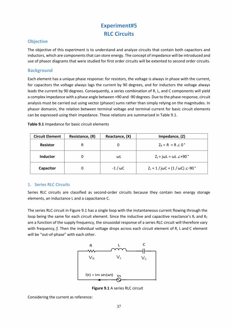
1. Series RLC Circuits
Series RLC circuits are classified as second-order circuits because they contain two energy storage
elements, an inductance L and a capacitance C.
The series RLC circuit in Figure 9.1 has a single loop with the instantaneous current flowing through the
loop being the same for each circuit element. Since the inductive and capacitive reactance’s XL and XC
are a function of the supply frequency, the sinusoidal response of a series RLC circuit will therefore vary
with frequency, ƒ. Then the individual voltage drops across each circuit element of R, L and C element
will be “out-of-phase” with each other.
Figure 9.1 A series RLC circuit
Considering the current as reference:
R
Vsİ(t) = Im sin(wt)
L C
VR VL VC
38
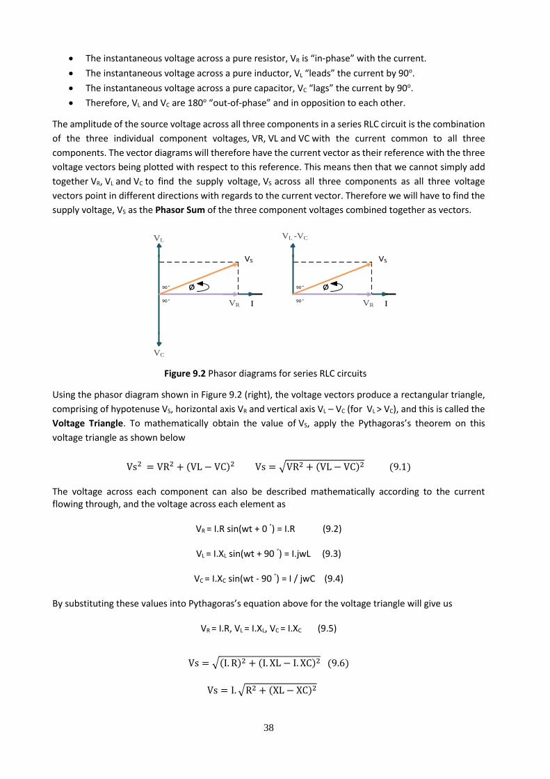
• The instantaneous voltage across a pure resistor, VR is “in-phase” with the current.
• The instantaneous voltage across a pure inductor, VL “leads” the current by 90o.
• The instantaneous voltage across a pure capacitor, VC “lags” the current by 90o.
• Therefore, VL and VC are 180o “out-of-phase” and in opposition to each other.
The amplitude of the source voltage across all three components in a series RLC circuit is the combination
of the three individual component voltages, VR, VL and VC with the current common to all three
components. The vector diagrams will therefore have the current vector as their reference with the three
voltage vectors being plotted with respect to this reference. This means then that we cannot simply add
together VR, VL and VC to find the supply voltage, VS across all three components as all three voltage
vectors point in different directions with regards to the current vector. Therefore we will have to find the
supply voltage, VS as the Phasor Sum of the three component voltages combined together as vectors.
Figure 9.2 Phasor diagrams for series RLC circuits
Using the phasor diagram shown in Figure 9.2 (right), the voltage vectors produce a rectangular triangle,
comprising of hypotenuse VS, horizontal axis VR and vertical axis VL – VC (for VL > VC), and this is called the
Voltage Triangle. To mathematically obtain the value of VS, apply the Pythagoras’s theorem on this
voltage triangle as shown below
Vs2 = VR2 + (VL − VC)2 Vs = √VR2 + (VL − VC)2 (9.1)
The voltage across each component can also be described mathematically according to the current flowing through, and the voltage across each element as
VR = I.R sin(wt + 0 °) = I.R (9.2)
VL = I.XL sin(wt + 90 °) = I.jwL (9.3)
VC = I.XC sin(wt - 90 °) = I / jwC (9.4)
By substituting these values into Pythagoras’s equation above for the voltage triangle will give us
VR = I.R, VL = I.XL, VC = I.XC (9.5)
Vs = √(I. R)2 + (I. XL − I. XC)2 (9.6)
Vs = I. √R2 + (XL − XC)2
IVR
VL
VC
VS
ø 90 °
90 °IVR
VL -VC
VS
ø 90 °
90 °
39
Vs=I.Z where Z = √R2 + (XL − XC)2
The impedance Z of a series RLC circuit depends upon the angular frequency, ω as do XL and XC. If the capacitive reactance is greater than the inductive reactance, XC > XL then the overall circuit reactance is capacitive giving a leading phase angle. Likewise, if the inductive reactance is greater than the capacitive reactance, XL > XC then the overall circuit reactance is inductive giving the series circuit a lagging phase angle. If the two reactance’s are the same and XL = XC then the angular frequency at which this occurs is called the resonant frequency and produces the effect of resonance. The impedance triangle for series RLC circuit is given in Figure 9.3 and the impedance is expressed as
Z = √R2 + (wL − 1/wC)2 (9.7) The phase angle, Ø between the source voltage, VS and the current, i is the same as for the angle between Z and R in the impedance triangle. This phase angle may be positive or negative in value depending on whether the source voltage leads or lags the circuit current and can be calculated mathematically from the ohmic values of the impedance triangle as
cosØ = R/Z (9.8)
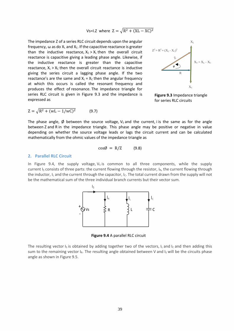
2. Parallel RLC Circuit
In Figure 9.4, the supply voltage, VS is common to all three components, while the supply current IS consists of three parts: the current flowing through the resistor, IR, the current flowing through the inductor, IL and the current through the capacitor, IC. The total current drawn from the supply will not be the mathematical sum of the three individual branch currents but their vector sum.
Figure 9.4 A parallel RLC circuit
The resulting vector IS is obtained by adding together two of the vectors, IL and IC and then adding this sum to the remaining vector IR. The resulting angle obtained between V and IS will be the circuits phase angle as shown in Figure 9.5.
ø
XL
XC
R
Z2 = R2 + (XL - XC)2
XT = XL – XC
RVs L C+
-
IS
IR IL IC
Figure 9.3 Impedance triangle for series RLC circuits
40
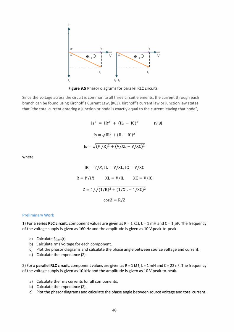
Figure 9.5 Phasor diagrams for parallel RLC circuits
Since the voltage across the circuit is common to all three circuit elements, the current through each
branch can be found using Kirchoff’s Current Law, (KCL). Kirchoff’s current law or junction law states
that “the total current entering a junction or node is exactly equal to the current leaving that node”,
Is2 = IR2 + (IL − IC)2 (9.9)
Is = √IR2 + (IL − IC)2
Is = √(V /R)2 + (V/XL − V/XC)2 where
IR = 𝑉/𝑅, IL = V/XL, IC = V/XC
R = 𝑉/𝐼𝑅 XL = V/IL XC = V/IC
Z = 1/√(1/R)2 + (1/XL − 1/XC)2
cosØ = R/Z
Preliminary Work
1) For a series RLC circuit, component values are given as R = 1 k, L = 1 mH and C = 1 𝜇F. The frequency of the voltage supply is given as 160 Hz and the amplitude is given as 10 V peak-to-peak.
a) Calculate is(rms)(t). b) Calculate rms voltage for each component. c) Plot the phasor diagrams and calculate the phase angle between source voltage and current. d) Calculate the impedance (Z).
2) For a parallel RLC circuit, component values are given as R = 1 k, L = 1 mH and C = 22 nF. The frequency of the voltage supply is given as 10 kHz and the amplitude is given as 10 V peak-to-peak.
a) Calculate the rms currents for all components. b) Calculate the impedance (Z). c) Plot the phasor diagrams and calculate the phase angle between source voltage and total current.
IR
V
IL
IS
ø
90 °
90 °
IC
IR
V
IL - IC
IS
ø 90 °

41
Procedure
1) For given circuit in Preliminary Work Q1,
a) Measure the current using multimeter
b) Measure the voltage for all components using multimeter.
c) Measure the phase difference between source voltage and current using oscilloscope and compare your result with Preliminary Work Q1(c).
d) Change the frequency between 100 Hz - 200 kHz and observe the effect of frequency on the resistor voltage.
2) For given circuit in Preliminary Work Q2,
a) Measure currents for each component using multimeter.
List of Equipment and Components
Equipment: Function Generator, Oscilloscope, Digital Multimeter
Components: a resistor of 1 kΩ, an inductor of 1 mH, capacitors of 1 𝜇F and 22 nF
42
Experiment#6
Low-Pass and High-Pass Filters Objective
The objective of this experiment is to understand and analyze two kinds of passive filters, low-pass filter
and high-pass filter. The effect of varying source frequency to the output voltage of these filters will be
studied. The cut-off frequency will be determined.
Background
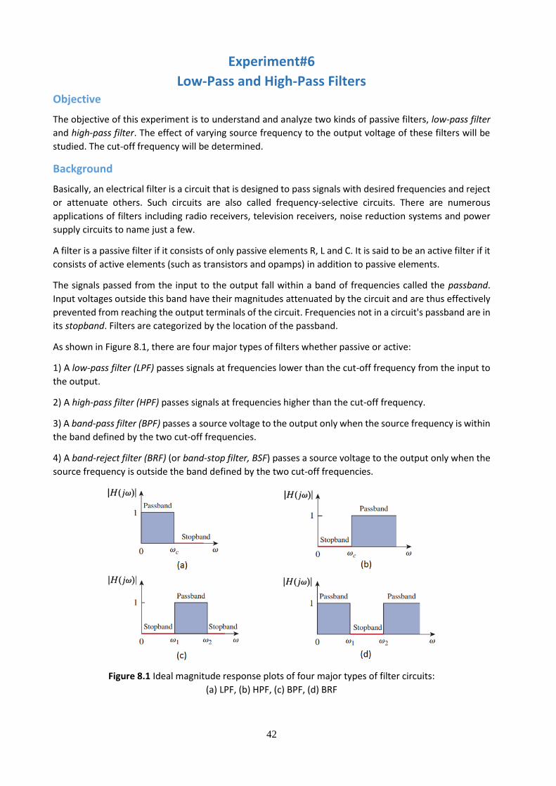
Basically, an electrical filter is a circuit that is designed to pass signals with desired frequencies and reject
or attenuate others. Such circuits are also called frequency-selective circuits. There are numerous
applications of filters including radio receivers, television receivers, noise reduction systems and power
supply circuits to name just a few.
A filter is a passive filter if it consists of only passive elements R, L and C. It is said to be an active filter if it
consists of active elements (such as transistors and opamps) in addition to passive elements.
The signals passed from the input to the output fall within a band of frequencies called the passband.
Input voltages outside this band have their magnitudes attenuated by the circuit and are thus effectively
prevented from reaching the output terminals of the circuit. Frequencies not in a circuit's passband are in
its stopband. Filters are categorized by the location of the passband.
As shown in Figure 8.1, there are four major types of filters whether passive or active:
1) A low-pass filter (LPF) passes signals at frequencies lower than the cut-off frequency from the input to
the output.
2) A high-pass filter (HPF) passes signals at frequencies higher than the cut-off frequency.
3) A band-pass filter (BPF) passes a source voltage to the output only when the source frequency is within
the band defined by the two cut-off frequencies.
4) A band-reject filter (BRF) (or band-stop filter, BSF) passes a source voltage to the output only when the
source frequency is outside the band defined by the two cut-off frequencies.
Figure 8.1 Ideal magnitude response plots of four major types of filter circuits:
(a) LPF, (b) HPF, (c) BPF, (d) BRF
43
1. Low-Pass Filter
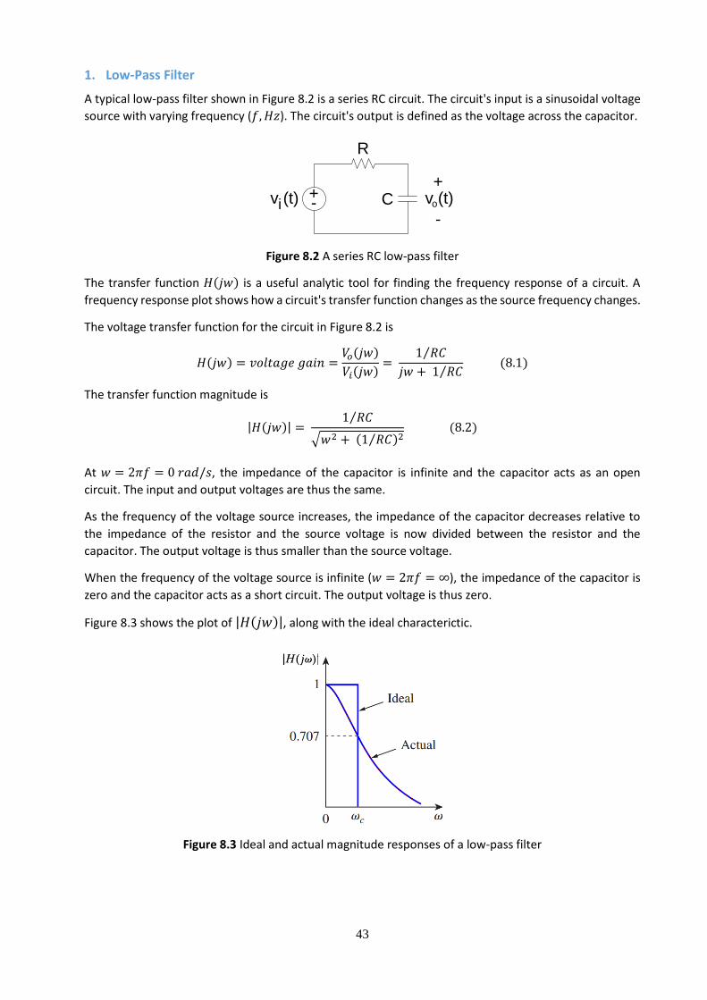
A typical low-pass filter shown in Figure 8.2 is a series RC circuit. The circuit's input is a sinusoidal voltage
source with varying frequency (𝑓, 𝐻𝑧). The circuit's output is defined as the voltage across the capacitor.
-+v (t)i v (t)o
R
C
-
+
Figure 8.2 A series RC low-pass filter
The transfer function 𝐻(𝑗𝑤) is a useful analytic tool for finding the frequency response of a circuit. A
frequency response plot shows how a circuit's transfer function changes as the source frequency changes.
The voltage transfer function for the circuit in Figure 8.2 is
𝐻(𝑗𝑤) = 𝑣𝑜𝑙𝑡𝑎𝑔𝑒 𝑔𝑎𝑖𝑛 =𝑉𝑜(𝑗𝑤)
𝑉𝑖(𝑗𝑤)=
1 𝑅𝐶⁄
𝑗𝑤 + 1 𝑅𝐶⁄ (8.1)
The transfer function magnitude is
|𝐻(𝑗𝑤)| = 1 𝑅𝐶⁄
√𝑤2 + (1 𝑅𝐶⁄ )2 (8.2)
At 𝑤 = 2𝜋𝑓 = 0 𝑟𝑎𝑑/𝑠, the impedance of the capacitor is infinite and the capacitor acts as an open
circuit. The input and output voltages are thus the same.
As the frequency of the voltage source increases, the impedance of the capacitor decreases relative to
the impedance of the resistor and the source voltage is now divided between the resistor and the
capacitor. The output voltage is thus smaller than the source voltage.
When the frequency of the voltage source is infinite (𝑤 = 2𝜋𝑓 = ∞), the impedance of the capacitor is
zero and the capacitor acts as a short circuit. The output voltage is thus zero.
Figure 8.3 shows the plot of |𝐻(𝑗𝑤)|, along with the ideal characterictic.
Figure 8.3 Ideal and actual magnitude responses of a low-pass filter
44
The cut-off frequency is the frequency at which the transfer function drops in magnitude to 70.7% of its
maximum value. We can then describe the relationship among the quantities 𝑅, 𝐶 and 𝑤𝑐 as follows,
|𝐻(𝑗𝑤𝑐)| = 1
√2(1) =
1 𝑅𝐶⁄
√𝑤𝑐2 + (1 𝑅𝐶⁄ )2
(8.3)
Solving this equation for 𝑤𝑐, we get
𝑤𝑐 = 1
𝑅𝐶 (8.4)
At the cut-off frequency 𝑤𝑐, the average power delivered by the circuit is one half the maximum average
power. Thus, 𝑤𝑐 is also called the half-power frequency. Therefore, in the passband, the average power
delivered to a load is at least 50% of the maximum average power.
The gain of a system is typically measured in decibel (dB). The dB value is a logarithmic measurement of
the ratio of one variable to another of the same type. For a voltage or current gain 𝐺, its dB equivalent is
𝐺𝑑𝐵 = 20 𝑙𝑜𝑔10𝐺. At the cut-off frequency, we have
20𝑙𝑜𝑔10(1 √2⁄ ) = −3 𝑑𝐵 (8.5)
2. High-Pass Filter
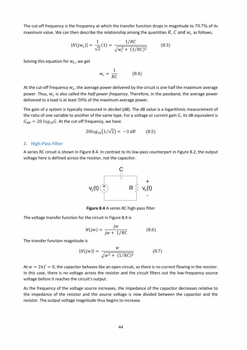
A series RC circuit is shown in Figure 8.4. In contrast to its low-pass counterpart in Figure 8.2, the output
voltage here is defined across the resistor, not the capacitor.
-+v (t)i v (t)oR
C
-
+
Figure 8.4 A series RC high-pass filter
The voltage transfer function for the circuit in Figure 8.4 is
𝐻(𝑗𝑤) = 𝑗𝑤
𝑗𝑤 + 1 𝑅𝐶⁄ (8.6)
The transfer function magnitude is
|𝐻(𝑗𝑤)| = 𝑤
√𝑤2 + (1 𝑅𝐶⁄ )2 (8.7)
At 𝑤 = 2𝜋𝑓 = 0, the capacitor behaves like an open circuit, so there is no current flowing in the resistor.
In this case, there is no voltage across the resistor and the circuit filters out the low-frequency source
voltage before it reaches the circuit's output.
As the frequency of the voltage source increases, the impedance of the capacitor decreases relative to
the impedance of the resistor and the source voltage is now divided between the capacitor and the
resistor. The output voltage magnitude thus begins to increase.
45
When the frequency of the voltage source is infinite (𝑤 = 2𝜋𝑓 = ∞), the capacitor behaves as a short
circuit, and thus there is no voltage across the capacitor. In this case, the input voltage and output voltage
are the same.
Figure 8.5 shows the plot of |𝐻(𝑗𝑤)|, along with the ideal characterictic.
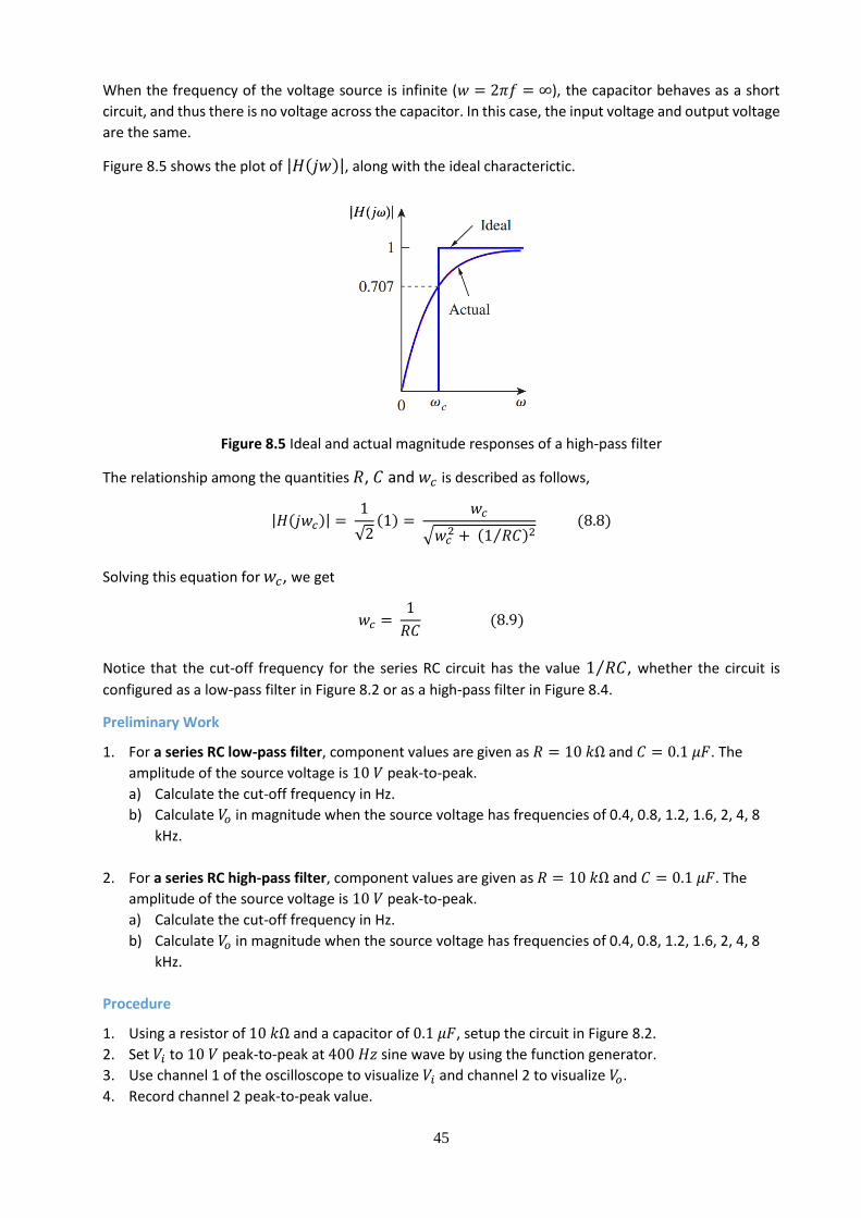
Figure 8.5 Ideal and actual magnitude responses of a high-pass filter
The relationship among the quantities 𝑅, 𝐶 and 𝑤𝑐 is described as follows,
|𝐻(𝑗𝑤𝑐)| = 1
√2(1) =
𝑤𝑐
√𝑤𝑐2 + (1 𝑅𝐶⁄ )2
(8.8)
Solving this equation for 𝑤𝑐, we get
𝑤𝑐 = 1
𝑅𝐶 (8.9)
Notice that the cut-off frequency for the series RC circuit has the value 1 𝑅𝐶⁄ , whether the circuit is
configured as a low-pass filter in Figure 8.2 or as a high-pass filter in Figure 8.4.
Preliminary Work
1. For a series RC low-pass filter, component values are given as 𝑅 = 10 𝑘Ω and 𝐶 = 0.1 𝜇𝐹. The
amplitude of the source voltage is 10 𝑉 peak-to-peak.
a) Calculate the cut-off frequency in Hz.
b) Calculate 𝑉𝑜 in magnitude when the source voltage has frequencies of 0.4, 0.8, 1.2, 1.6, 2, 4, 8
kHz.
2. For a series RC high-pass filter, component values are given as 𝑅 = 10 𝑘Ω and 𝐶 = 0.1 𝜇𝐹. The
amplitude of the source voltage is 10 𝑉 peak-to-peak.
a) Calculate the cut-off frequency in Hz.
b) Calculate 𝑉𝑜 in magnitude when the source voltage has frequencies of 0.4, 0.8, 1.2, 1.6, 2, 4, 8
kHz.
Procedure
1. Using a resistor of 10 𝑘Ω and a capacitor of 0.1 𝜇𝐹, setup the circuit in Figure 8.2.
2. Set 𝑉𝑖 to 10 𝑉 peak-to-peak at 400 𝐻𝑧 sine wave by using the function generator.
3. Use channel 1 of the oscilloscope to visualize 𝑉𝑖 and channel 2 to visualize 𝑉𝑜.
4. Record channel 2 peak-to-peak value.
46
5. Increase the source frequency as stated in Preliminary Work Q1(b). Record the channel 2 peak-to-
peak value each time you increase the frequency. Make sure that 𝑉𝑖 is maintaining at 10 𝑉 peak-to-
peak each time the frequency is increased.
6. Based on your results, plot 𝑉𝑜 versus frequency.
7. From the graph, find the cut-off frequency by tracing the frequency where the magnitude of the
output voltage is 70.7% of its maximum value.
8. Compare all your results with the Preliminary Work Q1.
9. Using a resistor of 10 𝑘Ω and a capacitor of 0.1 𝜇𝐹, setup the circuit in Figure 8.4 and repeat the steps
2-7. Compare all your results with the Preliminary Work Q2.
List of Equipment and Components
Equipment: Function Generator, Oscilloscope
Components: a resistor of 10 kΩ, a capacitor of 0.1 μF
References
[1] James W. Nilsson, Susan A. Riedel, Electric Circuits (Ninth Edition)
[2] Charles K. Alexander, Matthew N. O. Sadiku, Fundamentals of Electric Circuits (Fifth Edition)
47
Experiment#7
Resonance Circuits, Band-Pass and Band-Reject Filters
Objective
The objective of this experiment is to examine some of circuits constructed using resistors, capacitors and
inductors for inputs with different frequency values and understand the concept of resonance using series
and parallel resonance circuits. One other objective is to analyze band-pass and band-reject filter circuits.
Background
In previous experiments, we observed that in a circuit which contains only inductive component, the
voltage leads current by 90o but in a circuit containing only capacitance, the voltage lags behind the
current by 90o. Thus, the phase angle between the inductive and capacitive voltages is 180o and the two
voltages oppose each other. In circuits where inductors and capacitors are used together, the two more
or less oppose each other. If the inductive effect is greater than the capacitive effect, then the circuit will
act like an inductor in overall and the voltage will lead the current. On the other hand, if the capacitive
effect is greater than the inductive effect, the circuit will behave like a capacitor and the voltage will lag
behind the current. If, however, the inductive effect of the coil is exactly equal to the capacitive effect of
the capacitor, the two effect will cancel each other out and the voltage and current will be in phase. Such
a circuit is called a resonance circuit and the phenomenon is called resonance. There are two types of
resonant circuits which are series resonant circuits and parallel resonant circuits. These resonant circuits
are useful for constructing band-pass and band-reject filters.
1. Series Resonance Circuits
A pure inductance or coil (without resistance) is not
obtainable in practice. Any coil will have some resistance
depending upon the size of the wire used. Even the
capacitance and the connecting leads in an LC circuit will
have resistance [1]. So, any resonant LC circuit is actually
an RLC resonant circuit which is shown in Figure 10.1. The
impedance of the circuit is
𝑍 = √𝑅2 + (𝑋𝐿 − 𝑋𝐶)2 (10.1)
If the circuit is resonant to the frequency of the applied voltage 𝑉𝑠, then XL = XC and the impedance of the
circuit 𝑍 = √𝑅2 + 02 = 𝑅. The voltage across L and C are equal and opposite in phase and they cancel
out leaving only the resistance R in the circuit [1].
The circuit is resistive and the current I is given as below
𝐼 = 𝑉𝑠
𝑍=
𝑉𝑠
𝑅 (10.2)
The resonant frequency can be determined in terms of the inductance and capacitance by examining
the defining equation for resonance, XL = XC .
𝑋𝐿 = 𝑋𝐶 → 𝜔𝐿 = 1
𝜔𝐶→ 𝜔2 =
1
𝐿𝐶→ 𝜔𝑠 =
1
√𝐿𝐶
𝑓𝑠 =1
2𝜋√𝐿𝐶 (10.3)
A certain combination of L and C resonates at a particular frequency when the capacitive reactance
becomes equal to the inductive reactance. At this frequency, the impedance of the circuit is minimum and
Figure 10.1 Series resonant circuit
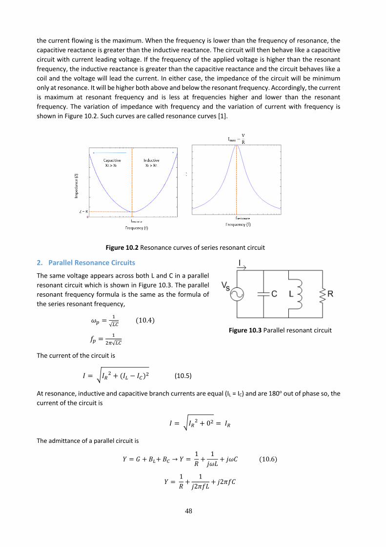
48
the current flowing is the maximum. When the frequency is lower than the frequency of resonance, the
capacitive reactance is greater than the inductive reactance. The circuit will then behave like a capacitive
circuit with current leading voltage. If the frequency of the applied voltage is higher than the resonant
frequency, the inductive reactance is greater than the capacitive reactance and the circuit behaves like a
coil and the voltage will lead the current. In either case, the impedance of the circuit will be minimum
only at resonance. It will be higher both above and below the resonant frequency. Accordingly, the current
is maximum at resonant frequency and is less at frequencies higher and lower than the resonant
frequency. The variation of impedance with frequency and the variation of current with frequency is
shown in Figure 10.2. Such curves are called resonance curves [1].
Figure 10.2 Resonance curves of series resonant circuit
2. Parallel Resonance Circuits
The same voltage appears across both L and C in a parallel
resonant circuit which is shown in Figure 10.3. The parallel
resonant frequency formula is the same as the formula of
the series resonant frequency,
𝜔𝑝 =1
√𝐿𝐶 (10.4)
𝑓𝑝 =1
2𝜋√𝐿𝐶
The current of the circuit is
𝐼 = √𝐼𝑅2 + (𝐼𝐿 − 𝐼𝐶)2 (10.5)
At resonance, inductive and capacitive branch currents are equal (IL = IC) and are 180o out of phase so, the
current of the circuit is
𝐼 = √𝐼𝑅2 + 02 = 𝐼𝑅
The admittance of a parallel circuit is
𝑌 = 𝐺 + 𝐵𝐿+ 𝐵𝐶 → 𝑌 = 1
𝑅+
1
𝑗𝜔𝐿+ 𝑗𝜔𝐶 (10.6)
𝑌 = 1
𝑅+
1
𝑗2𝜋𝑓𝐿+ 𝑗2𝜋𝑓𝐶
Figure 10.3 Parallel resonant circuit
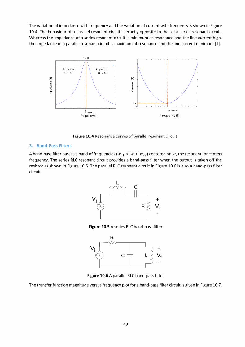
49
The variation of impedance with frequency and the variation of current with frequency is shown in Figure
10.4. The behaviour of a parallel resonant circuit is exactly opposite to that of a series resonant circuit.
Whereas the impedance of a series resonant circuit is minimum at resonance and the line current high,
the impedance of a parallel resonant circuit is maximum at resonance and the line current minimum [1].
Figure 10.4 Resonance curves of parallel resonant circuit
3. Band-Pass Filters
A band-pass filter passes a band of frequencies (𝑤𝑐1 < 𝑤 < 𝑤𝑐2) centered on 𝑤, the resonant (or center)
frequency. The series RLC resonant circuit provides a band-pass filter when the output is taken off the
resistor as shown in Figure 10.5. The parallel RLC resonant circuit in Figure 10.6 is also a band-pass filter
circuit.
V io
-
+R
CL
AC V
Figure 10.5 A series RLC band-pass filter
R
C LAC
V io
-
+V
Figure 10.6 A parallel RLC band-pass filter
The transfer function magnitude versus frequency plot for a band-pass filter circuit is given in Figure 10.7.
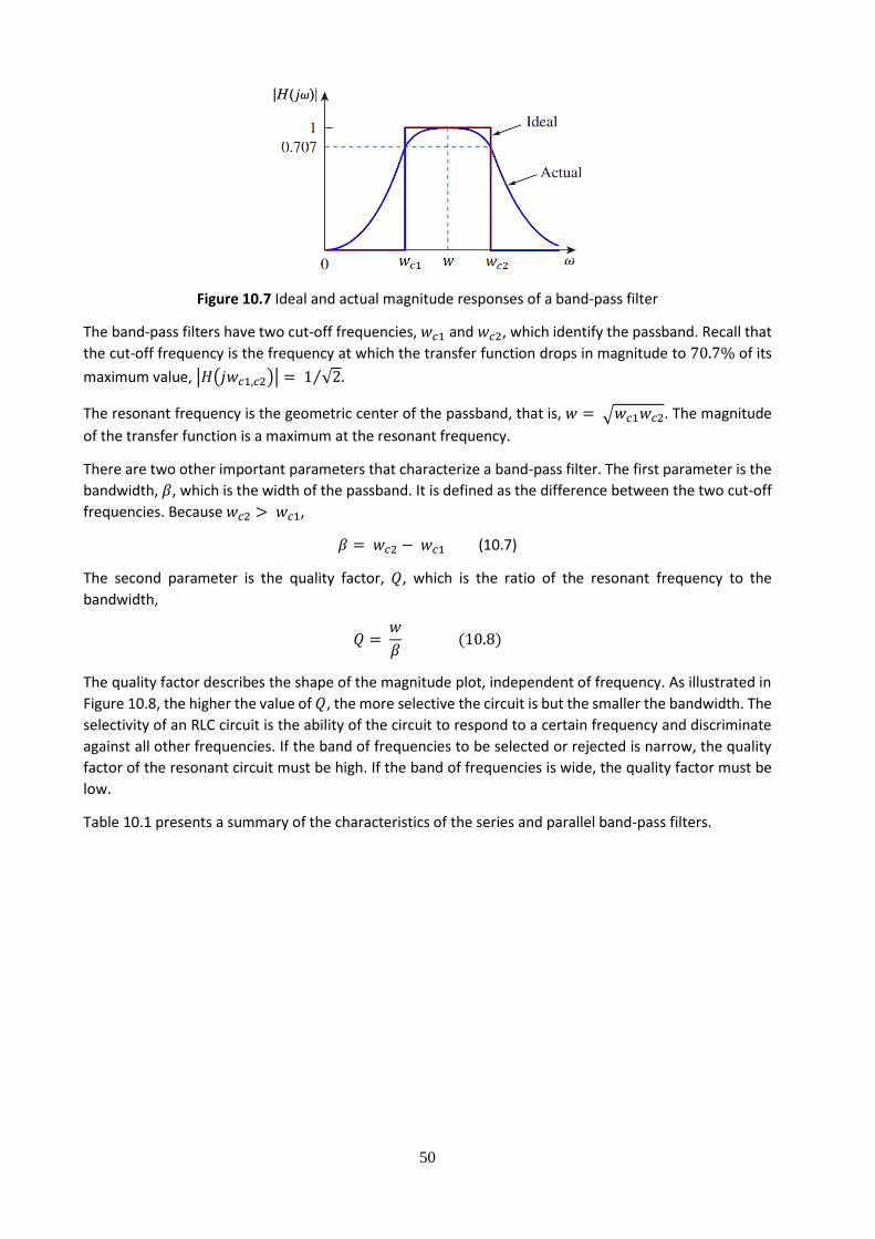
50
Figure 10.7 Ideal and actual magnitude responses of a band-pass filter
The band-pass filters have two cut-off frequencies, 𝑤𝑐1 and 𝑤𝑐2, which identify the passband. Recall that
the cut-off frequency is the frequency at which the transfer function drops in magnitude to 70.7% of its
maximum value, |𝐻(𝑗𝑤𝑐1,𝑐2)| = 1 √2⁄ .
The resonant frequency is the geometric center of the passband, that is, 𝑤 = √𝑤𝑐1𝑤𝑐2. The magnitude
of the transfer function is a maximum at the resonant frequency.
There are two other important parameters that characterize a band-pass filter. The first parameter is the
bandwidth, 𝛽, which is the width of the passband. It is defined as the difference between the two cut-off
frequencies. Because 𝑤𝑐2 > 𝑤𝑐1,
𝛽 = 𝑤𝑐2 − 𝑤𝑐1 (10.7)
The second parameter is the quality factor, 𝑄, which is the ratio of the resonant frequency to the
bandwidth,
𝑄 = 𝑤
𝛽 (10.8)
The quality factor describes the shape of the magnitude plot, independent of frequency. As illustrated in
Figure 10.8, the higher the value of 𝑄, the more selective the circuit is but the smaller the bandwidth. The
selectivity of an RLC circuit is the ability of the circuit to respond to a certain frequency and discriminate
against all other frequencies. If the band of frequencies to be selected or rejected is narrow, the quality
factor of the resonant circuit must be high. If the band of frequencies is wide, the quality factor must be
low.
Table 10.1 presents a summary of the characteristics of the series and parallel band-pass filters.
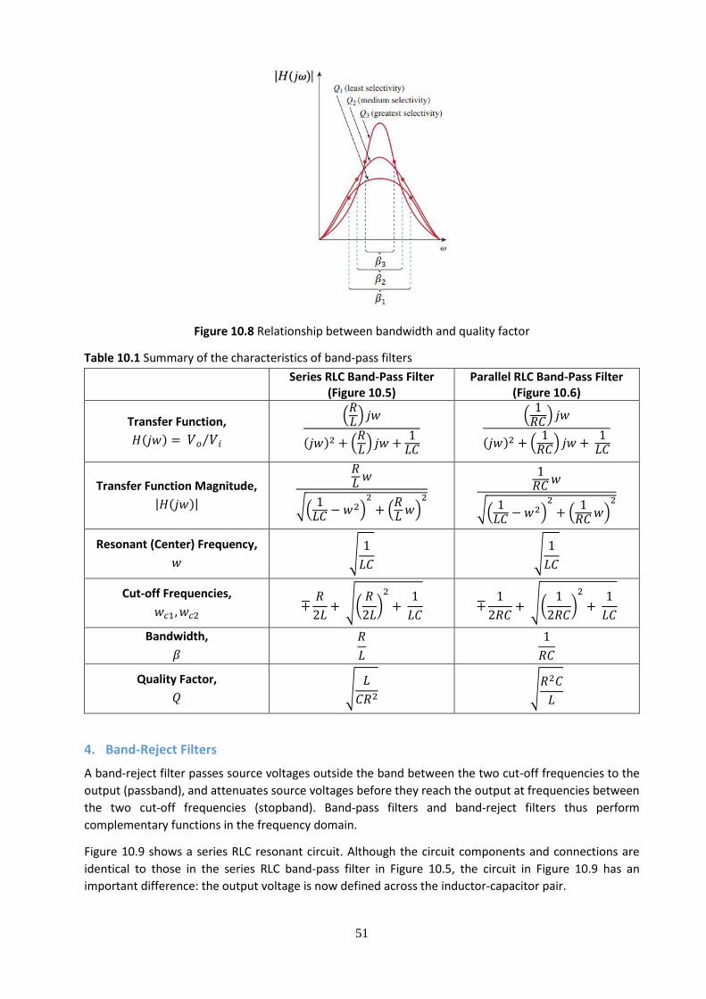
51
Figure 10.8 Relationship between bandwidth and quality factor
Table 10.1 Summary of the characteristics of band-pass filters
Series RLC Band-Pass Filter
(Figure 10.5) Parallel RLC Band-Pass Filter
(Figure 10.6)
Transfer Function,
𝐻(𝑗𝑤) = 𝑉𝑜 𝑉𝑖⁄
(𝑅𝐿
) 𝑗𝑤
(𝑗𝑤)2 + (𝑅𝐿) 𝑗𝑤 +
1𝐿𝐶
(
1𝑅𝐶
) 𝑗𝑤
(𝑗𝑤)2 + (1
𝑅𝐶) 𝑗𝑤 + 1
𝐿𝐶
Transfer Function Magnitude,
|𝐻(𝑗𝑤)|
𝑅𝐿 𝑤
√(1
𝐿𝐶− 𝑤2)
2
+ (𝑅𝐿
𝑤)2
1𝑅𝐶
𝑤
√(1
𝐿𝐶− 𝑤2)
2
+ (1
𝑅𝐶𝑤)
2
Resonant (Center) Frequency,
𝑤 √
1
𝐿𝐶 √
1
𝐿𝐶
Cut-off Frequencies,
𝑤𝑐1, 𝑤𝑐2 ∓𝑅
2𝐿+ √(
𝑅
2𝐿)
2
+ 1
𝐿𝐶 ∓
1
2𝑅𝐶+ √(
1
2𝑅𝐶)
2
+ 1
𝐿𝐶
Bandwidth,
𝛽
𝑅
𝐿
1
𝑅𝐶
Quality Factor,
𝑄 √
𝐿
𝐶𝑅2 √
𝑅2𝐶
𝐿
4. Band-Reject Filters
A band-reject filter passes source voltages outside the band between the two cut-off frequencies to the
output (passband), and attenuates source voltages before they reach the output at frequencies between
the two cut-off frequencies (stopband). Band-pass filters and band-reject filters thus perform
complementary functions in the frequency domain.
Figure 10.9 shows a series RLC resonant circuit. Although the circuit components and connections are
identical to those in the series RLC band-pass filter in Figure 10.5, the circuit in Figure 10.9 has an
important difference: the output voltage is now defined across the inductor-capacitor pair.
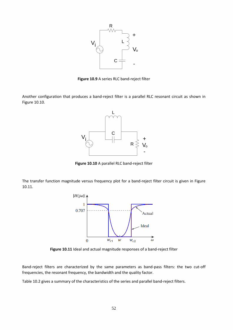
52
V io
-
+
R
C
AC V
L
Figure 10.9 A series RLC band-reject filter
Another configuration that produces a band-reject filter is a parallel RLC resonant circuit as shown in
Figure 10.10.
AC
L
C
R
V io
-
+V
Figure 10.10 A parallel RLC band-reject filter
The transfer function magnitude versus frequency plot for a band-reject filter circuit is given in Figure
10.11.
Figure 10.11 Ideal and actual magnitude responses of a band-reject filter
Band-reject filters are characterized by the same parameters as band-pass filters: the two cut-off
frequencies, the resonant frequency, the bandwidth and the quality factor.
Table 10.2 gives a summary of the characteristics of the series and parallel band-reject filters.
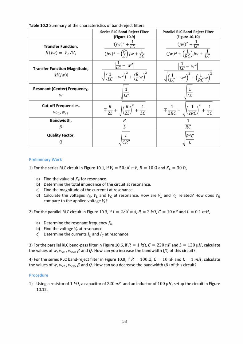
53
Table 10.2 Summary of the characteristics of band-reject filters
Series RLC Band-Reject Filter
(Figure 10.9) Parallel RLC Band-Reject Filter
(Figure 10.10)
Transfer Function,
𝐻(𝑗𝑤) = 𝑉𝑜 𝑉𝑖⁄
(𝑗𝑤)2 +1
𝐿𝐶
(𝑗𝑤)2 + (𝑅𝐿
) 𝑗𝑤 +1
𝐿𝐶
(𝑗𝑤)2 +
1𝐿𝐶
(𝑗𝑤)2 + (1
𝑅𝐶) 𝑗𝑤 +
1𝐿𝐶
Transfer Function Magnitude,
|𝐻(𝑗𝑤)|
|1
𝐿𝐶− 𝑤2|
√(1
𝐿𝐶− 𝑤2)
2
+ (𝑅𝐿
𝑤)2
|
1𝐿𝐶 − 𝑤2|
√(1
𝐿𝐶− 𝑤2)
2
+ (1
𝑅𝐶𝑤)
2
Resonant (Center) Frequency,
𝑤 √
1
𝐿𝐶 √
1
𝐿𝐶
Cut-off Frequencies,
𝑤𝑐1, 𝑤𝑐2 ∓𝑅
2𝐿+ √(
𝑅
2𝐿)
2
+ 1
𝐿𝐶 ∓
1
2𝑅𝐶+ √(
1
2𝑅𝐶)
2
+ 1
𝐿𝐶
Bandwidth,
𝛽
𝑅
𝐿
1
𝑅𝐶
Quality Factor,
𝑄 √
𝐿
𝐶𝑅2 √
𝑅2𝐶
𝐿
Preliminary Work
1) For the series RLC circuit in Figure 10.1, if 𝑉𝑠 = 50∠0° 𝑚𝑉, 𝑅 = 10 Ω and 𝑋𝐿 = 30 Ω,
a) Find the value of 𝑋𝐶 for resonance. b) Determine the total impedance of the circuit at resonance. c) Find the magnitude of the current I at resonance. d) Calculate the voltages 𝑉𝑅, 𝑉𝐿 and 𝑉𝐶 at resonance. How are 𝑉𝐿 and 𝑉𝐶 related? How does 𝑉𝑅
compare to the applied voltage 𝑉𝑠?
2) For the parallel RLC circuit in Figure 10.3, if 𝐼 = 2∠0° 𝑚𝐴, 𝑅 = 2 𝑘Ω, 𝐶 = 10 nF and 𝐿 = 0.1 𝑚𝐻,
a) Determine the resonant frequency 𝑓𝑝.
b) Find the voltage 𝑉𝑐 at resonance. c) Determine the currents 𝐼𝐿 and 𝐼𝐶 at resonance.
3) For the parallel RLC band-pass filter in Figure 10.6, if 𝑅 = 1 𝑘Ω, 𝐶 = 220 𝑛𝐹 and 𝐿 = 120 μ𝐻, calculate the values of 𝑤, 𝑤𝑐1, 𝑤𝑐2, 𝛽 and 𝑄. How can you increase the bandwidth (𝛽) of this circuit?
4) For the series RLC band-reject filter in Figure 10.9, if 𝑅 = 100 Ω, 𝐶 = 10 nF and 𝐿 = 1 𝑚𝐻, calculate the values of 𝑤, 𝑤𝑐1, 𝑤𝑐2, 𝛽 and 𝑄. How can you decrease the bandwidth (𝛽) of this circuit?
Procedure
1) Using a resistor of 1 𝑘Ω, a capacitor of 220 𝑛𝐹 and an inductor of 100 μ𝐻, setup the circuit in Figure
10.12.
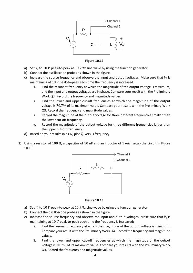
54
C LAC
V io
-
+V
R
Channel 1
Channel 2
Figure 10.12
a) Set 𝑉𝑖 to 10 𝑉 peak-to-peak at 10 𝑘𝐻𝑧 sine wave by using the function generator.
b) Connect the oscilloscope probes as shown in the figure.
c) Increase the source frequency and observe the input and output voltages. Make sure that 𝑉𝑖 is
maintaining at 10 𝑉 peak-to-peak each time the frequency is increased:
i. Find the resonant frequency at which the magnitude of the output voltage is maximum,
and the input and output voltages are in phase. Compare your result with the Preliminary
Work Q3. Record the frequency and magnitude values.
ii. Find the lower and upper cut-off frequencies at which the magnitude of the output
voltage is 70.7% of its maximum value. Compare your results with the Preliminary Work
Q3. Record the frequency and magnitude values.
iii. Record the magnitude of the output voltage for three different frequencies smaller than
the lower cut-off frequency.
iv. Record the magnitude of the output voltage for three different frequencies larger than
the upper cut-off frequency.
d) Based on your results in c.i-iv, plot 𝑉𝑜 versus frequency.
2) Using a resistor of 100 Ω, a capacitor of 10 nF and an inductor of 1 𝑚𝐻, setup the circuit in Figure
10.13.
Vs
R CL
AC
Channel 1
Channel 2
Figure 10.13
a) Set 𝑉𝑖 to 10 𝑉 peak-to-peak at 15 𝑘𝐻𝑧 sine wave by using the function generator.
b) Connect the oscilloscope probes as shown in the figure.
c) Increase the source frequency and observe the input and output voltages. Make sure that 𝑉𝑖 is
maintaining at 10 𝑉 peak-to-peak each time the frequency is increased:
i. Find the resonant frequency at which the magnitude of the output voltage is minimum.
Compare your result with the Preliminary Work Q4. Record the frequency and magnitude
values.
ii. Find the lower and upper cut-off frequencies at which the magnitude of the output
voltage is 70.7% of its maximum value. Compare your results with the Preliminary Work
Q4. Record the frequency and magnitude values.
55
iii. Record the magnitude of the output voltage for three different frequencies smaller than
the lower cut-off frequency.
iv. Record the magnitude of the output voltage for three different frequencies larger than
the upper cut-off frequency.
d) Based on your results in c.i-iv, plot 𝑉𝑜 versus frequency.
List of Equipment and Components
Equipment: Function generator, Oscilloscope
Components: resistors of 100Ω, 1 kΩ, capacitors of 220 nF and 10 nF, inductors of 100 μH and 1 mH
References
[1] Sharma, Basic Radio & Television, 2/E
[2] Boylestad, Introductory Circuit Analysis (Tenth Edition)
[3] James W. Nilsson, Susan A. Riedel, Electric Circuits (Ninth Edition)
[4] Charles K. Alexander, Matthew N. O. Sadiku, Fundamentals of Electric Circuits (Fifth Edition)
56
APPENDIX A International System of Units
The Interational System of Units (SI) is used by most engineering thoughout the world and will be used
in this course as well [1].
The SI units are based on seven defined quantities: length, mass, time, electric current, thermodynamic
temparature, amount of substance and luminous intensity. These quantities are listed in Table A.1
together with the basic unit and symbol.
Table A.1 The International System of Units (SI)
Quantity Basic Unit Symbol
Length meter m
Mass kilogram Kg
Time second s
Electric current ampere A
Thermodynamic temperature degree kelvin K
Amount of substance mole mol
Luminous intensity Candela cd
Defined quantities are combined to form derived units. Some of these quantities, such as force, power,
electric charge etc. are given in Table A.2
Table A.2 Derived units in SI
Quantity Basic Unit Symbol
Frequency hertz (Hz) s-1
Force newton (N) kg ∙ m/s2
Energy or Work joule (J) N ∙ m
Power watt (W) J/s
Electric charge coulomb (C) A ∙ s
Electric potential volt (V) J/C
Electric resistance ohm (Ω) V/A
Electric conductance siemens (S) A/V
Electric capacitance farad (F) C/V
Magnetic flux weber (Wb) V ∙ s
Inductance henry (H) Wb/A
In many cases, the SI unit is either too smal or too large to use conveniently. Standard prefixes
corresponding to powers of 10, are listed in Table A.3.
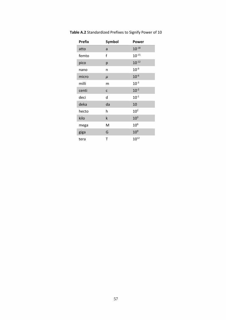
57
Table A.2 Standardized Prefixes to Signify Power of 10
Prefix Symbol Power
atto a 10-18
femto f 10-15
pico p 10-12
nano n 10-9
micro μ 10-6
milli m 10-3
centi c 10-2
deci d 10-1
deka da 10
hecto h 102
kilo k 103
mega M 106
giga G 109
tera T 1012
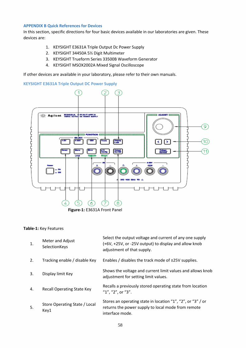
58
APPENDIX B Quick References for Devices
In this section, specific directions for four basic devices available in our laboratories are given. These
devices are:
1. KEYSIGHT E3631A Triple Output Dc Power Supply
2. KEYSIGHT 34450A 5½ Digit Multimeter
3. KEYSIGHT Trueform Series 33500B Waveform Generator
4. KEYSIGHT MSOX2002A Mixed Signal Oscilloscope
If other devices are available in your laboratory, please refer to their own manuals.
KEYSIGHT E3631A Triple Output DC Power Supply
Figure-1: E3631A Front Panel
Table-1: Key Features
1. Meter and Adjust
SelectionKeys
Select the output voltage and current of any one supply
(+6V, +25V, or -25V output) to display and allow knob
adjustment of that supply.
2. Tracking enable / disable Key Enables / disables the track mode of ±25V supplies.
3. Display limit Key Shows the voltage and current limit values and allows knob
adjustment for setting limit values.
4. Recall Operating State Key Recalls a previously stored operating state from location
“1”, “2”, or “3”.
5. Store Operating State / Local
Key1
Stores an operating state in location “1”, “2”, or “3” / or
returns the power supply to local mode from remote
interface mode.
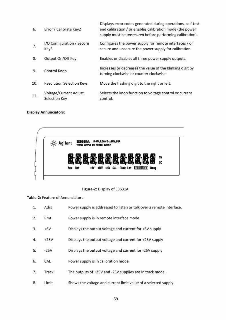
59
6. Error / Calibrate Key2
Displays error codes generated during operations, self-test
and calibration / or enables calibration mode (the power
supply must be unsecured before performing calibration).
7. I/O Configuration / Secure
Key3
Configures the power supply for remote interfaces / or
secure and unsecure the power supply for calibration.
8. Output On/Off Key Enables or disables all three power supply outputs.
9. Control Knob Increases or decreases the value of the blinking digit by
turning clockwise or counter clockwise.
10. Resolution Selection Keys Move the flashing digit to the right or left.
11. Voltage/Current Adjust
Selection Key
Selects the knob function to voltage control or current
control.
Display Annunciators:
Figure-2: Display of E3631A
Table-2: Feature of Annunciators
1. Adrs Power supply is addressed to listen or talk over a remote interface.
2. Rmt Power supply is in remote interface mode
3. +6V Displays the output voltage and current for +6V supply
4. +25V Displays the output voltage and current for +25V supply
5. -25V Displays the output voltage and current for -25V supply
6. CAL Power supply is in calibration mode
7. Track The outputs of +25V and -25V supplies are in track mode.
8. Limit Shows the voltage and current limit value of a selected supply.
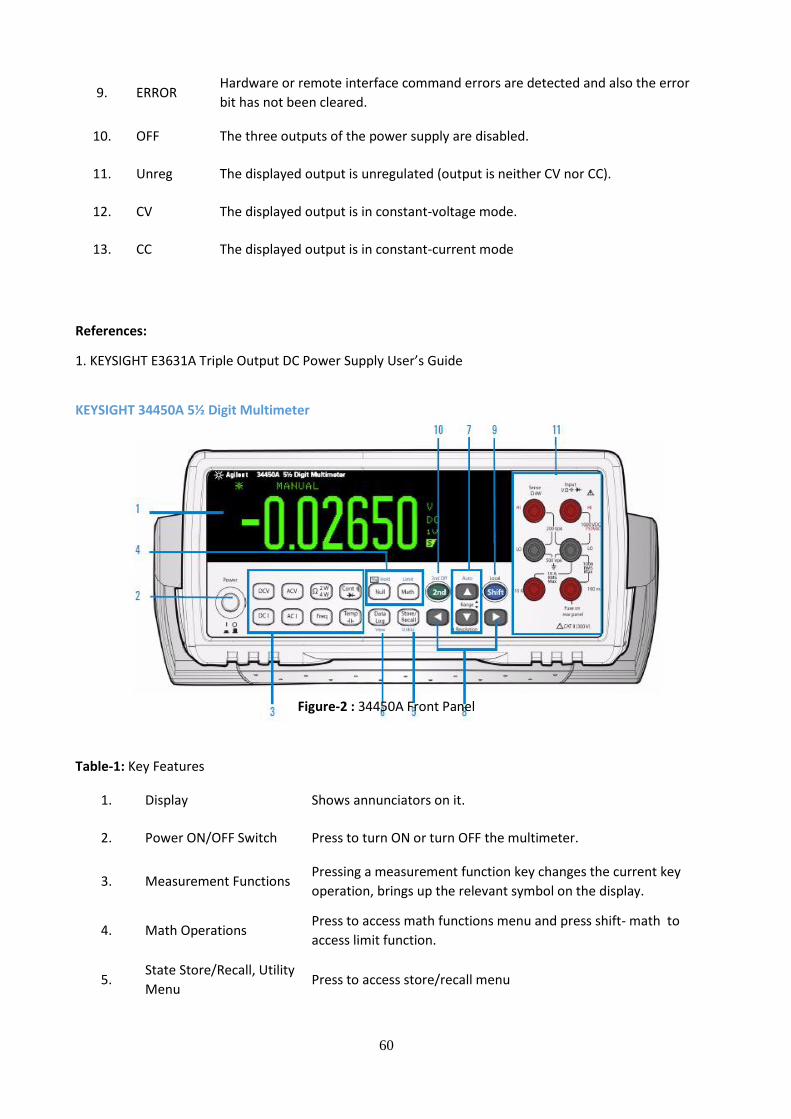
60
9. ERROR Hardware or remote interface command errors are detected and also the error
bit has not been cleared.
10. OFF The three outputs of the power supply are disabled.
11. Unreg The displayed output is unregulated (output is neither CV nor CC).
12. CV The displayed output is in constant-voltage mode.
13. CC The displayed output is in constant-current mode
References:
1. KEYSIGHT E3631A Triple Output DC Power Supply User’s Guide
KEYSIGHT 34450A 5½ Digit Multimeter
Figure-2 : 34450A Front Panel
Table-1: Key Features
1. Display Shows annunciators on it.
2. Power ON/OFF Switch Press to turn ON or turn OFF the multimeter.
3. Measurement Functions Pressing a measurement function key changes the current key
operation, brings up the relevant symbol on the display.
4. Math Operations Press to access math functions menu and press shift- math to
access limit function.
5. State Store/Recall, Utility
Menu Press to access store/recall menu
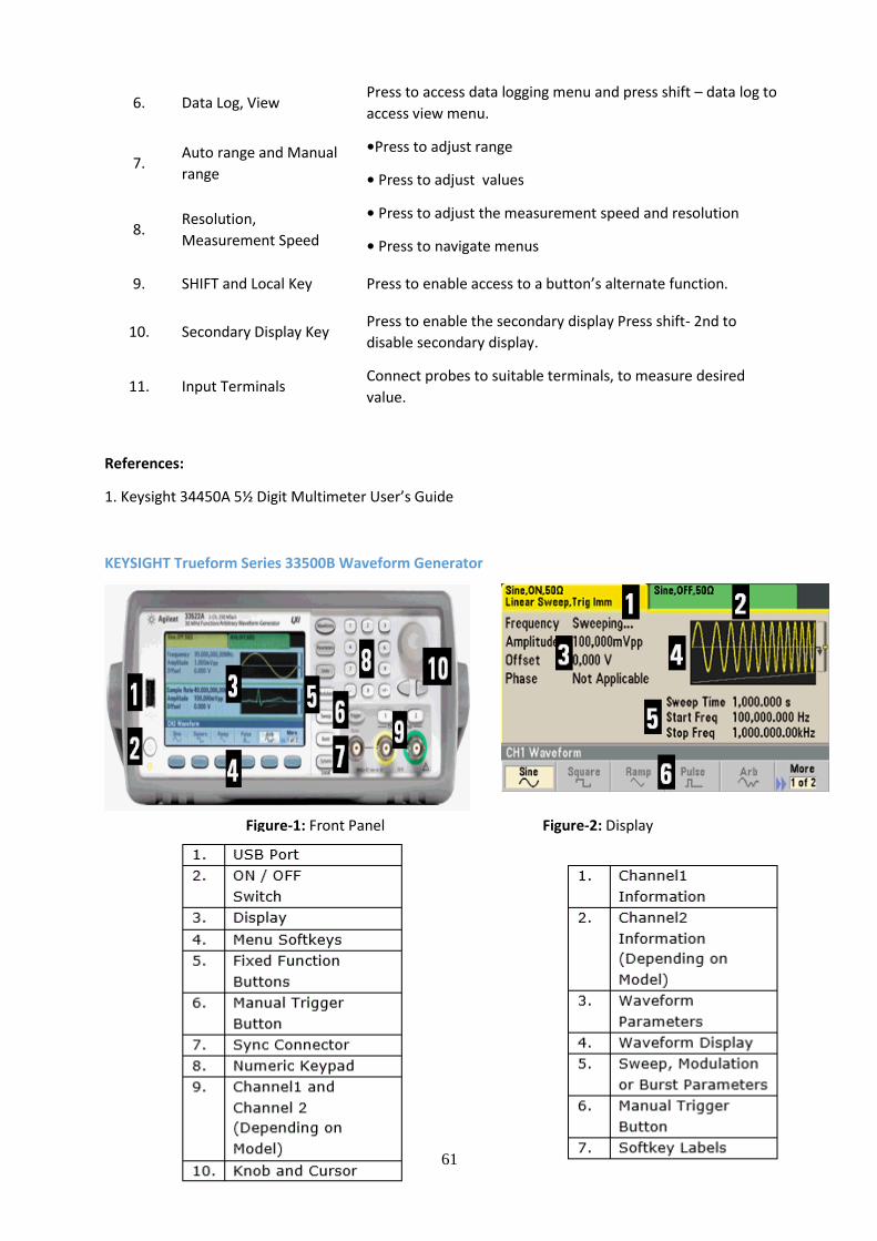
61
6. Data Log, View Press to access data logging menu and press shift – data log to
access view menu.
7. Auto range and Manual
range
•Press to adjust range
• Press to adjust values
8. Resolution,
Measurement Speed
• Press to adjust the measurement speed and resolution
• Press to navigate menus
9. SHIFT and Local Key Press to enable access to a button’s alternate function.
10. Secondary Display Key Press to enable the secondary display Press shift- 2nd to
disable secondary display.
11. Input Terminals Connect probes to suitable terminals, to measure desired
value.
References:
1. Keysight 34450A 5½ Digit Multimeter User’s Guide
KEYSIGHT Trueform Series 33500B Waveform Generator
Figure-1: Front Panel Figure-2: Display
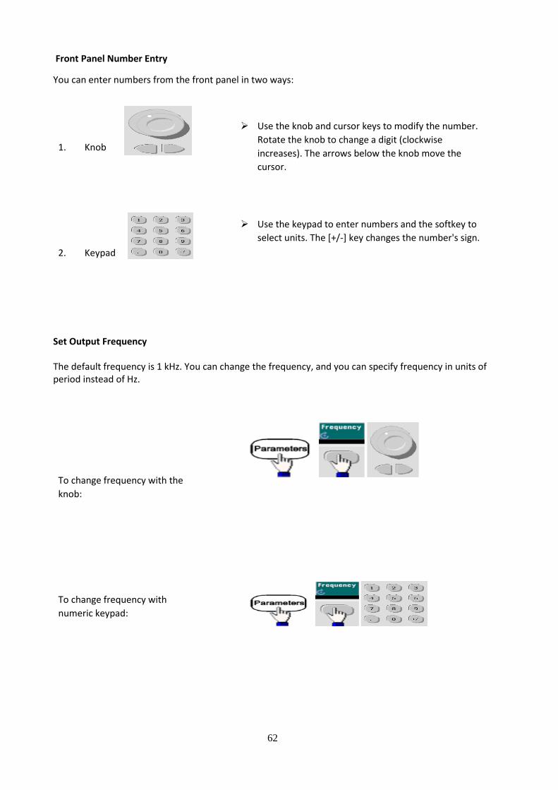
62
Front Panel Number Entry
You can enter numbers from the front panel in two ways:
1.
Knob
Use the knob and cursor keys to modify the number.
Rotate the knob to change a digit (clockwise
increases). The arrows below the knob move the
cursor.
2.
Keypad
Use the keypad to enter numbers and the softkey to
select units. The [+/-] key changes the number's sign.
Set Output Frequency The default frequency is 1 kHz. You can change the frequency, and you can specify frequency in units of period instead of Hz.
To change frequency with the
knob:
To change frequency with
numeric keypad:
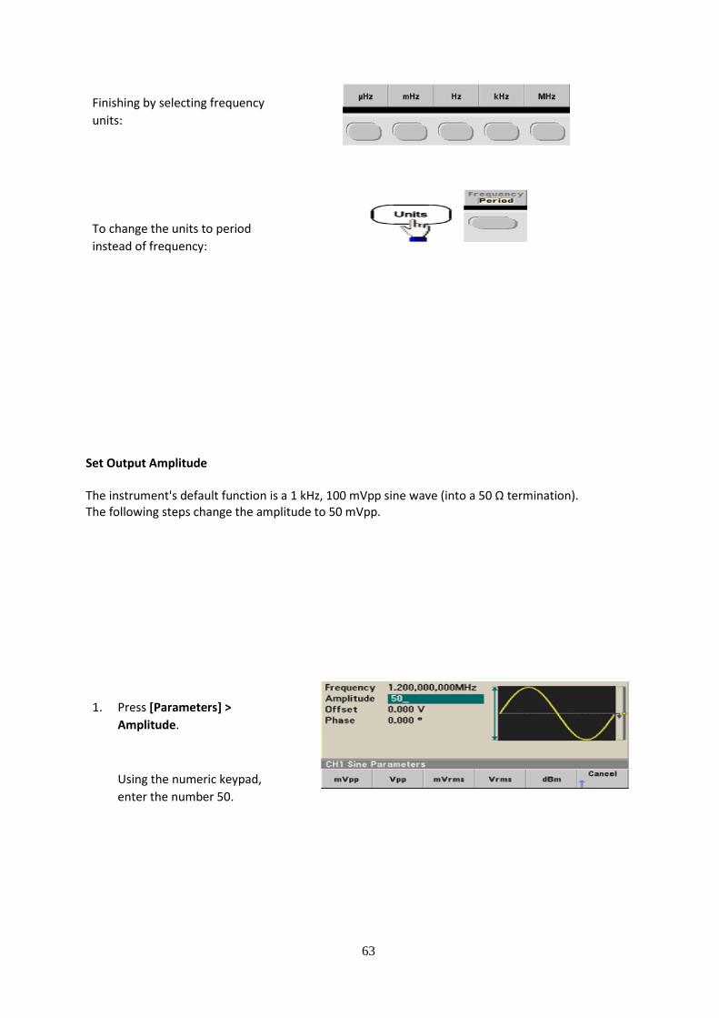
63
Finishing by selecting frequency
units:
To change the units to period
instead of frequency:
Set Output Amplitude The instrument's default function is a 1 kHz, 100 mVpp sine wave (into a 50 Ω termination). The following steps change the amplitude to 50 mVpp.
1.
Press [Parameters] >
Amplitude.
Using the numeric keypad,
enter the number 50.
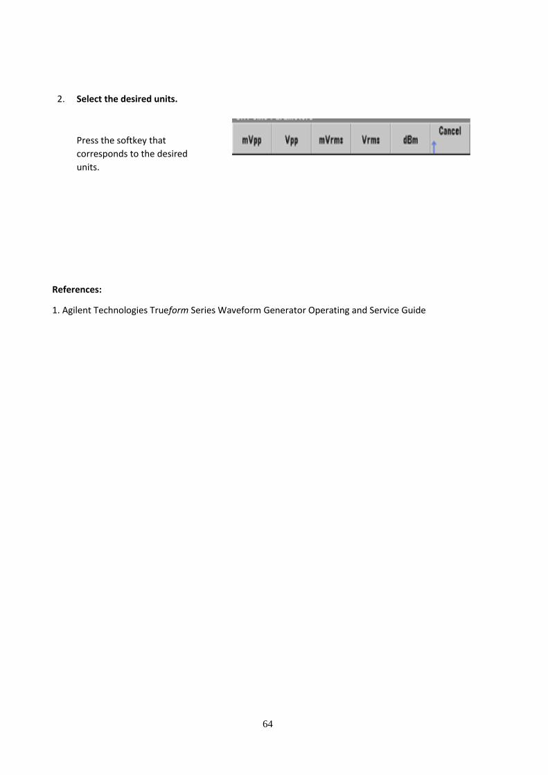
64
2.
Select the desired units.
Press the softkey that
corresponds to the desired
units.
References:
1. Agilent Technologies Trueform Series Waveform Generator Operating and Service Guide
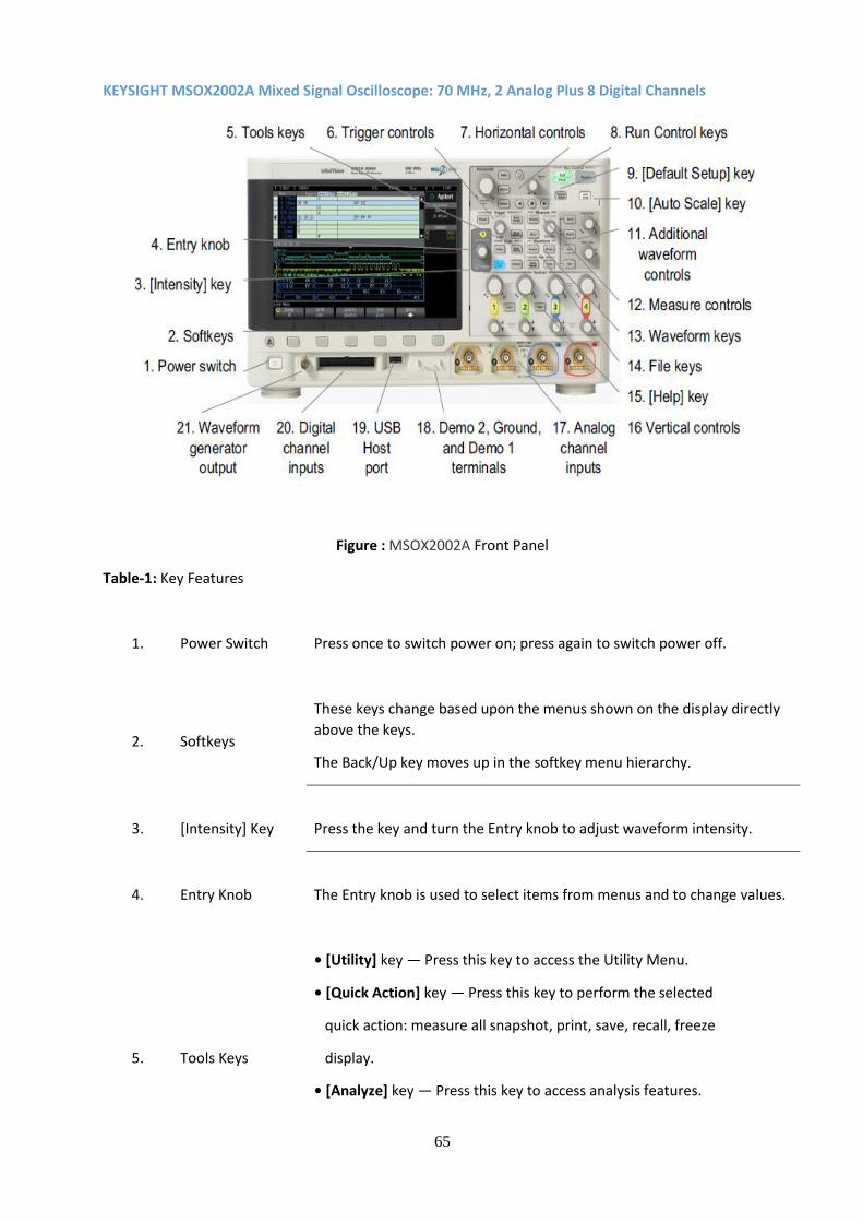
65
KEYSIGHT MSOX2002A Mixed Signal Oscilloscope: 70 MHz, 2 Analog Plus 8 Digital Channels
Figure : MSOX2002A Front Panel
Table-1: Key Features
1.
Power Switch
Press once to switch power on; press again to switch power off.
2.
Softkeys
These keys change based upon the menus shown on the display directly
above the keys.
The Back/Up key moves up in the softkey menu hierarchy.
3.
[Intensity] Key
Press the key and turn the Entry knob to adjust waveform intensity.
4.
Entry Knob
The Entry knob is used to select items from menus and to change values.
5.
Tools Keys
• [Utility] key — Press this key to access the Utility Menu.
• [Quick Action] key — Press this key to perform the selected
quick action: measure all snapshot, print, save, recall, freeze
display.
• [Analyze] key — Press this key to access analysis features.
66
• [Wave Gen] key — Press this key to access waveform
generator functions.
6.
Trigger Controls
These controls determine how the oscilloscope triggers to capture data.
7.
Horizontal
Controls
• Horizontal scale knob — : Turn the knob in the
Horizontal section to adjust the time/div (sweep speed) setting.
• Horizontal position knob to pan through the waveform
data horizontally.
8.
Run Control
keys
When the [Run/Stop] key is green, the oscilloscope is running, that is,
acquiring data when trigger conditions are met. To stop acquiring data,
press [Run/Stop].
9.
[Default Setup]
key
Press this key to restore the oscilloscope's default settings
10.
[Auto Scale]
key
When you press the [AutoScale] key, the oscilloscope will turn the active
channels on and scale them to display the input signals.
11.
Additional
Waveform
Controls
• [Math] key: Provides access to math (add, subtract, etc.)
waveform functions.
• [Ref] key: Provides access to reference waveform functions.
• [Digital] key: Press this key to turn the digital channels on
or off.
• [Serial] key: This key is used to enable serial decode.
12.
Measure
[Meas] key: Press this key to access a set of predefined
67
controls measurements.
13.
Waveform Keys
The [Acquire] key lets you select Normal, Peak Detect, Averaging, or High
Resolution acquisition modes.
The [Display] key lets you access the display menu.
14.
File Keys
Press the [Save/Recall] key to save or recall a waveform or setup.
15.
Help Key
Opens the Help Menu where you can display overview help topics and
select the Language.
16.
Vertical
Controls
•Use the big knobs to change the vertical sensitivity (gain) of
each analog channel.
•Use the little knobs to change a channel's vertical position on
the display.
17.
Analog Channel
Inputs
Analog input channels of oscilloscope are here.
References:
1. Keysight 34450A 5½ Digit Multimeter User’s Guide