Embed Size (px)
Citation preview

D. Breton2, C.Cheikali2, E. Delagnes1,, H. Grabas1,3,
O. Lemaire2, J. Maalmi2, P. Rusquart2, P. Vallerand2
1
1 CEA/IRFU Saclay (France)2 CNRS/IN2P3/LAL Orsay (France)3 Formerly CEA/IRFU Saclay (France)
This work has been initially funded by the P2IO LabEx (ANR-10-LABX-0038)
in the framework « Investissements d’Avenir » (ANR-11-IDEX-0003-01)
managed by the French National Research Agency (ANR)The TICAL ERC project (grant number 338953 from EU; PI: Paul Lecoq) has also
contributed to the developments of the TOT features integrated in the chip
FAST ELECTRONICS FOR TOF
IN NUCLEAR PHYSICS
FATA 2019 – Acireale - Sicily
| PAGE 2
INTRODUCTION
• Time stamping with picosecond (ps) accuracy is an emerging technique opening new fields
for nuclear & particle physics and medical instrumentation.
• It indeed permits the localization of vertices with a few mm precision, thus helping
associating particles coming from a common primary interaction even in a high background
(like for HL-LHC). It can also be used for particle identification based on Time of Flight
techniques.
• Time to Digital Converters (TDCs) are the usual natural candidates for time stamping of
fast signals.
• But the progress in ultra-fast digitizers (including high-end oscilloscopes) demonstrated that
ps timing accuracy can be reached simply by sampling the detector signal at high rate
and extracting time information by interpolation of the samples located in the leading edge
of the signal.
• Another advantage of recording the waveform resides in cases where the shape of the
detector signal (especially the leading edge) carries extra information in addition to direct
measurements (time, amplitude, etc.).
• But getting the full signal waveform has a non-negligible cost, especially at high rates (a few
tens of k€ per channel for a high-end oscilloscope).
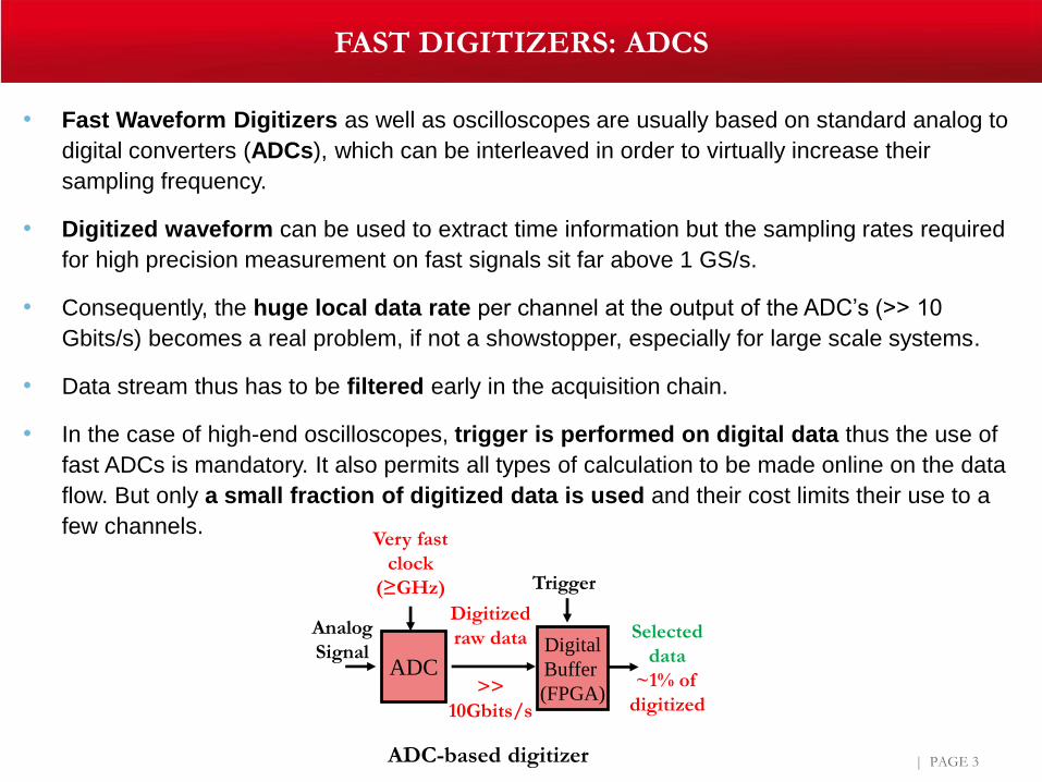
FAST DIGITIZERS: ADCS
| PAGE 3
• Fast Waveform Digitizers as well as oscilloscopes are usually based on standard analog to
digital converters (ADCs), which can be interleaved in order to virtually increase their
sampling frequency.
• Digitized waveform can be used to extract time information but the sampling rates required
for high precision measurement on fast signals sit far above 1 GS/s.
• Consequently, the huge local data rate per channel at the output of the ADC’s (>> 10
Gbits/s) becomes a real problem, if not a showstopper, especially for large scale systems.
• Data stream thus has to be filtered early in the acquisition chain.
• In the case of high-end oscilloscopes, trigger is performed on digital data thus the use of
fast ADCs is mandatory. It also permits all types of calculation to be made online on the data
flow. But only a small fraction of digitized data is used and their cost limits their use to a
few channels.
ADC
Analog
Signal
Very fast
clock
(≥GHz)
Digitized
raw data
>>
10Gbits/s
Digital
Buffer
(FPGA)
Trigger
Selected
data
~1% of
digitized
ADC-based digitizer
| PAGE 4
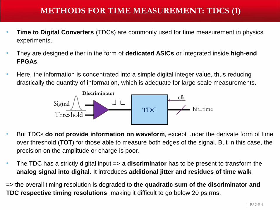
METHODS FOR TIME MEASUREMENT: TDCS (1)
• Time to Digital Converters (TDCs) are commonly used for time measurement in physics
experiments.
• They are designed either in the form of dedicated ASICs or integrated inside high-end
FPGAs.
• Here, the information is concentrated into a simple digital integer value, thus reducing
drastically the quantity of information, which is adequate for large scale measurements.
• But TDCs do not provide information on waveform, except under the derivate form of time
over threshold (TOT) for those able to measure both edges of the signal. But in this case, the
precision on the amplitude or charge is poor.
• The TDC has a strictly digital input => a discriminator has to be present to transform the
analog signal into digital. It introduces additional jitter and residues of time walk
=> the overall timing resolution is degraded to the quadratic sum of the discriminator and
TDC respective timing resolutions, making it difficult to go below 20 ps rms.
Discriminator
Signal
Threshold
clk
TDC hit_time
PAGE 5
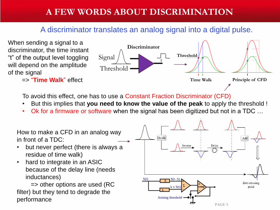
A FEW WORDS ABOUT DISCRIMINATION
When sending a signal to a
discriminator, the time instant
“t” of the output level toggling
will depend on the amplitude
of the signal
=> “Time Walk” effect
Discriminator
Signal
Threshold
t
Time Walk
Threshold
To avoid this effect, one has to use a Constant Fraction Discriminator (CFD)
• But this implies that you need to know the value of the peak to apply the threshold !
• Ok for a firmware or software when the signal has been digitized but not in a TDC …
How to make a CFD in an analog way
in front of a TDC:
• but never perfect (there is always a
residue of time walk)
• hard to integrate in an ASIC
because of the delay line (needs
inductances)
=> other options are used (RC
filter) but they tend to degrade the
performance
Principle of CFD
k
Δ +
-
S(t) S(t-Δ)
k x S(t) Σ
-
+comp
Arming threshold
A discriminator translates an analog signal into a digital pulse.
| PAGE 6
METHODS FOR TIME MEASUREMENT: TDCS (2)
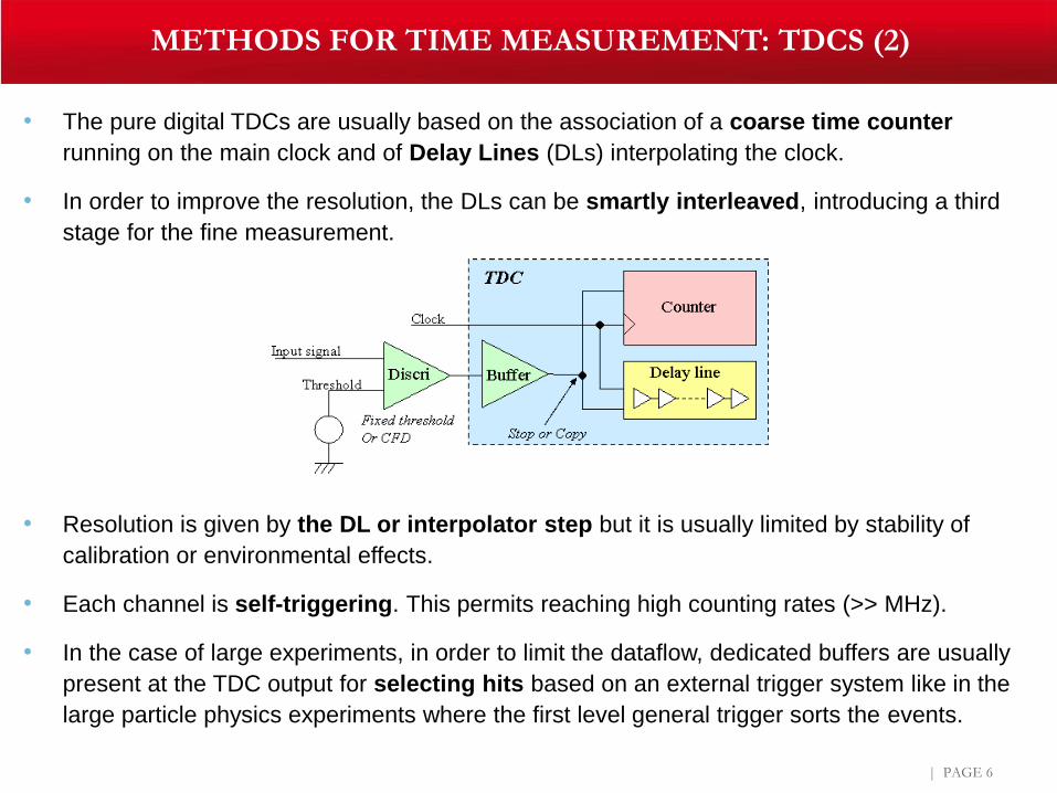
• The pure digital TDCs are usually based on the association of a coarse time counter
running on the main clock and of Delay Lines (DLs) interpolating the clock.
• In order to improve the resolution, the DLs can be smartly interleaved, introducing a third
stage for the fine measurement.
• Resolution is given by the DL or interpolator step but it is usually limited by stability of
calibration or environmental effects.
• Each channel is self-triggering. This permits reaching high counting rates (>> MHz).
• In the case of large experiments, in order to limit the dataflow, dedicated buffers are usually
present at the TDC output for selecting hits based on an external trigger system like in the
large particle physics experiments where the first level general trigger sorts the events.
FAST DIGITIZERS: ANALOG MEMORIES…
| PAGE 7
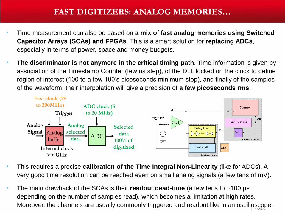
• Time measurement can also be based on a mix of fast analog memories using Switched
Capacitor Arrays (SCAs) and FPGAs. This is a smart solution for replacing ADCs,
especially in terms of power, space and money budgets.
• The discriminator is not anymore in the critical timing path. Time information is given by
association of the Timestamp Counter (few ns step), of the DLL locked on the clock to define
region of interest (100 to a few 100’s picoseconds minimum step), and finally of the samples
of the waveform: their interpolation will give a precision of a few picoseconds rms.
• This requires a precise calibration of the Time Integral Non-Linearity (like for ADCs). A
very good time resolution can be reached even on small analog signals (a few tens of mV).
• The main drawback of the SCAs is their readout dead-time (a few tens to ~100 µs
depending on the number of samples read), which becomes a limitation at high rates.
Moreover, the channels are usually commonly triggered and readout like in an oscilloscope.
Analog
buffer
Analog
Signal
Fast clock (25
to 200MHz)
Analog
selected
data ADC
Trigger
ADC clock (5
to 20 MHz)
Selected
data
100% of
digitizedInternal clock
>> GHz
| PAGE 8
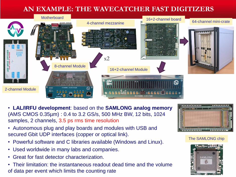
AN EXAMPLE: THE WAVECATCHER FAST DIGITIZERS
• LAL/IRFU development: based on the SAMLONG analog memory
(AMS CMOS 0.35µm) : 0.4 to 3.2 GS/s, 500 MHz BW, 12 bits, 1024
samples, 2 channels, 3.5 ps rms time resolution
• Autonomous plug and play boards and modules with USB and
secured Gbit UDP interfaces (copper or optical link).
• Powerful software and C libraries available (Windows and Linux).
• Used worldwide in many labs and companies.
• Great for fast detector characterization.
• Their limitation: the instantaneous readout dead time and the volume
of data per event which limits the counting rate
Motherboard
4-channel mezzanine
x2
16+2-channel board
16+2-channel Module8-channel Module
64-channel mini-crate
The SAMLONG chip
2-channel Module
| PAGE 9
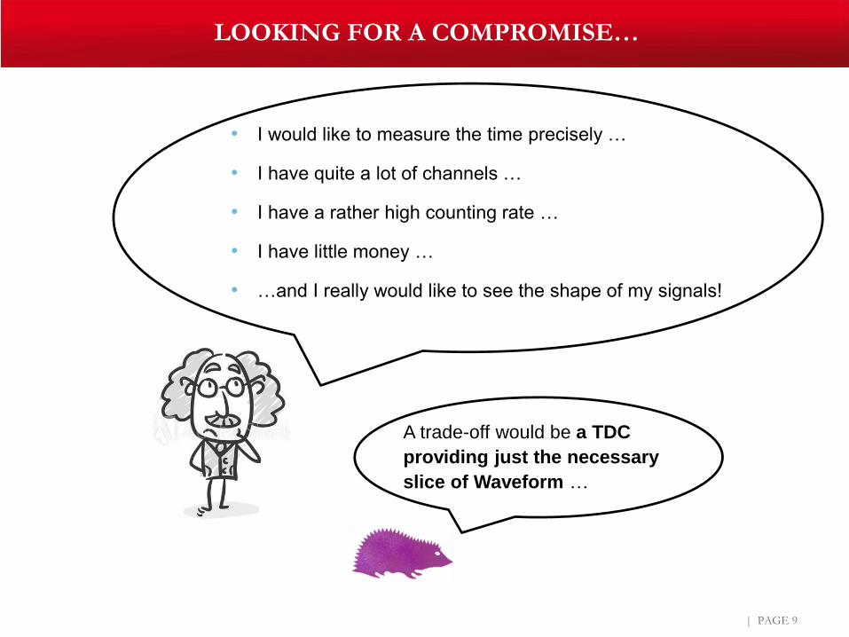
LOOKING FOR A COMPROMISE…
• I would like to measure the time precisely …
• I have quite a lot of channels …
• I have a rather high counting rate …
• I have little money …
• …and I really would like to see the shape of my signals!
A trade-off would be a TDC
providing just the necessary
slice of Waveform …
An
An+1
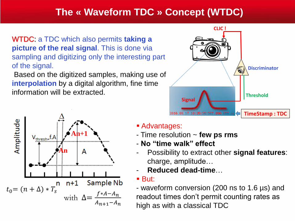
WTDC: a TDC which also permits taking a
picture of the real signal. This is done via
sampling and digitizing only the interesting part
of the signal.
Based on the digitized samples, making use of
interpolation by a digital algorithm, fine time
information will be extracted.
The « Waveform TDC » Concept (WTDC)
with ∆=𝑓∗𝐴−𝐴𝑛
𝐴𝑛+1−𝐴𝑛
Advantages:
- Time resolution ~ few ps rms
- No “time walk” effect
- Possibility to extract other signal features:
charge, amplitude…
- Reduced dead-time…
But:
- waveform conversion (200 ns to 1.6 µs) and
readout times don’t permit counting rates as
high as with a classical TDC
𝑡0= (𝑛 + Δ) ∗ 𝑇𝑠
TimeStamp : TDC
Discriminator
Threshold
CLIC !
Signal
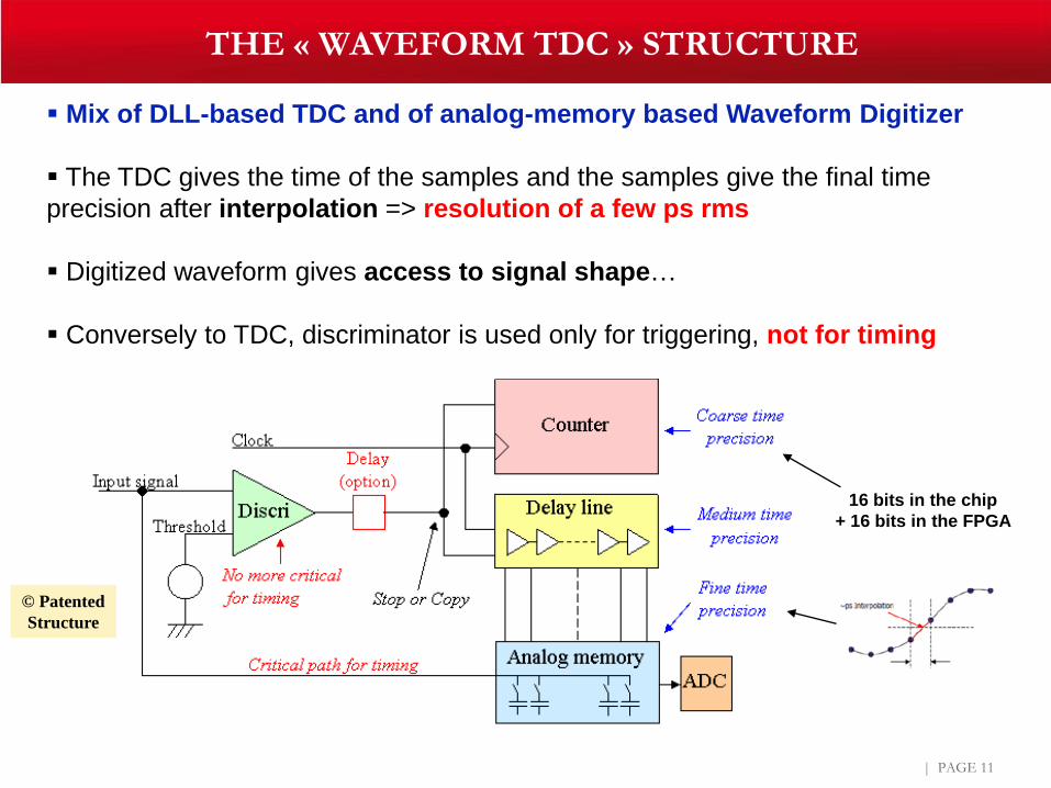
THE « WAVEFORM TDC » STRUCTURE
| PAGE 11
Mix of DLL-based TDC and of analog-memory based Waveform Digitizer
The TDC gives the time of the samples and the samples give the final time
precision after interpolation => resolution of a few ps rms
Digitized waveform gives access to signal shape…
Conversely to TDC, discriminator is used only for triggering, not for timing
16 bits in the chip
+ 16 bits in the FPGA
© Patented
Structure
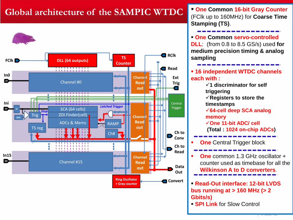
Global architecture of the SAMPIC WTDC
| PAGE 12
One Common 16-bit Gray Counter
(FClk up to 160MHz) for Coarse Time
Stamping (TS).
One Common servo-controlled
DLL: (from 0.8 to 8.5 GS/s) used for
medium precision timing & analog
sampling
16 independent WTDC channels
each with :1 discriminator for self
triggering
Registers to store the
timestamps
64-cell deep SCA analog
memory
One 11-bit ADC/ cell
(Total : 1024 on-chip ADCs)
One Central Trigger block
One common 1.3 GHz oscillator +
counter used as timebase for all the
Wilkinson A to D converters.
Read-Out interface: 12-bit LVDS
bus running at > 160 MHz (> 2
Gbits/s)
SPI Link for Slow Control
DLL (64 outputs)
Ring Oscillator+ Gray counter
TS regRAMP
DAC
Stop
Latched Trigger
Trig
Ch#
Channel
Readout
Channel
Readout
Channel #15
Channel
Readout
TS Counter
Convert
Read
Ch toConv
Ch toRead
RClk
DataOut
Channel #0
ADCs & Mems
ZOI Finder(cell)SCA (64 cells)
In0
Ini
In15
FClk
CentralTrigger
ExtTrig
IT
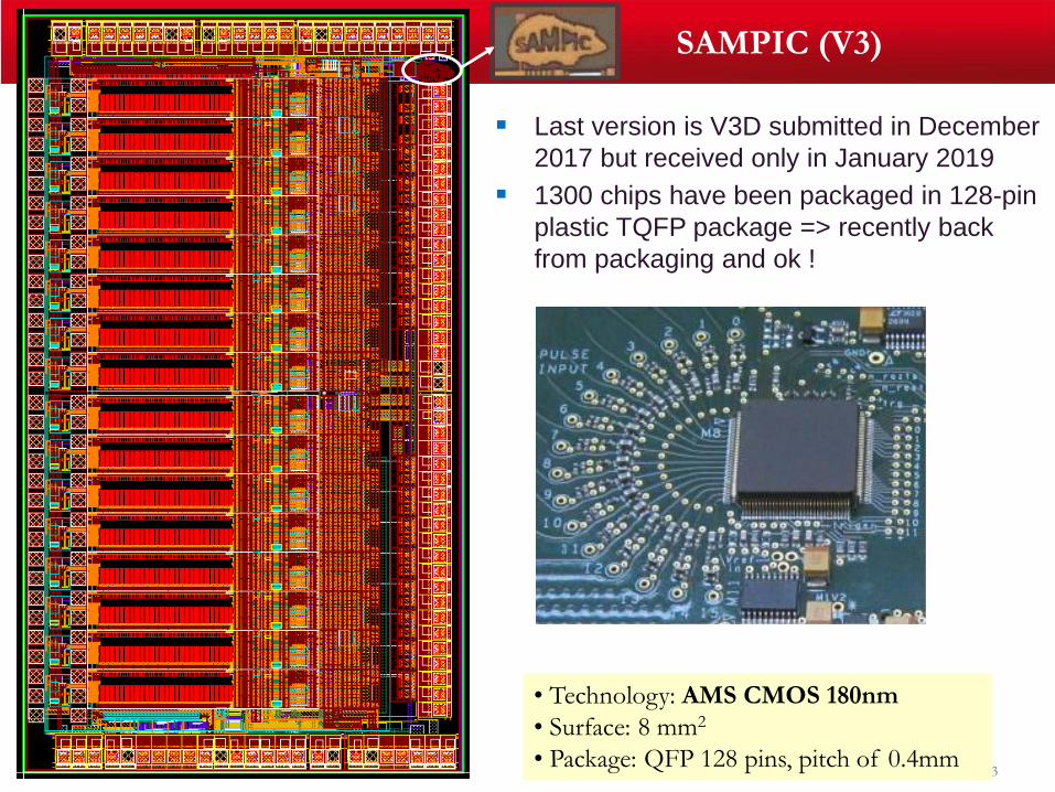
SAMPIC (V3)
| PAGE 13
• Technology: AMS CMOS 180nm
• Surface: 8 mm2
• Package: QFP 128 pins, pitch of 0.4mm
Last version is V3D submitted in December
2017 but received only in January 2019
1300 chips have been packaged in 128-pin
plastic TQFP package => recently back
from packaging and ok !
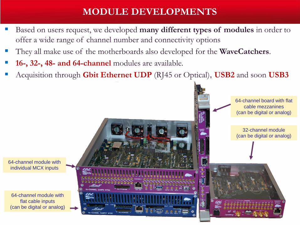
MODULE DEVELOPMENTS
Based on users request, we developed many different types of modules in order to
offer a wide range of channel number and connectivity options
They all make use of the motherboards also developed for the WaveCatchers.
16-, 32-, 48- and 64-channel modules are available.
Acquisition through Gbit Ethernet UDP (RJ45 or Optical), USB2 and soon USB3
64-channel module withindividual MCX inputs
64-channel module with
flat cable inputs(can be digital or analog)
64-channel board with flat
cable mezzanines(can be digital or analog)
32-channel module(can be digital or analog)
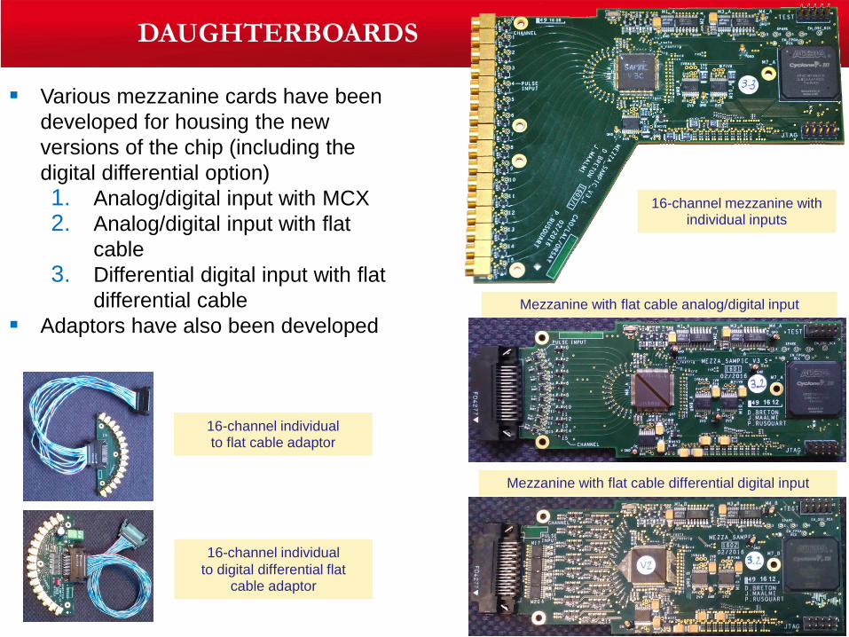
DAUGHTERBOARDS
Various mezzanine cards have been
developed for housing the new
versions of the chip (including the
digital differential option)
1. Analog/digital input with MCX
2. Analog/digital input with flat
cable
3. Differential digital input with flat
differential cable
Adaptors have also been developedMezzanine with flat cable analog/digital input
Mezzanine with flat cable differential digital input
16-channel individualto flat cable adaptor
16-channel individual
to digital differential flat cable adaptor
16-channel mezzanine withindividual inputs
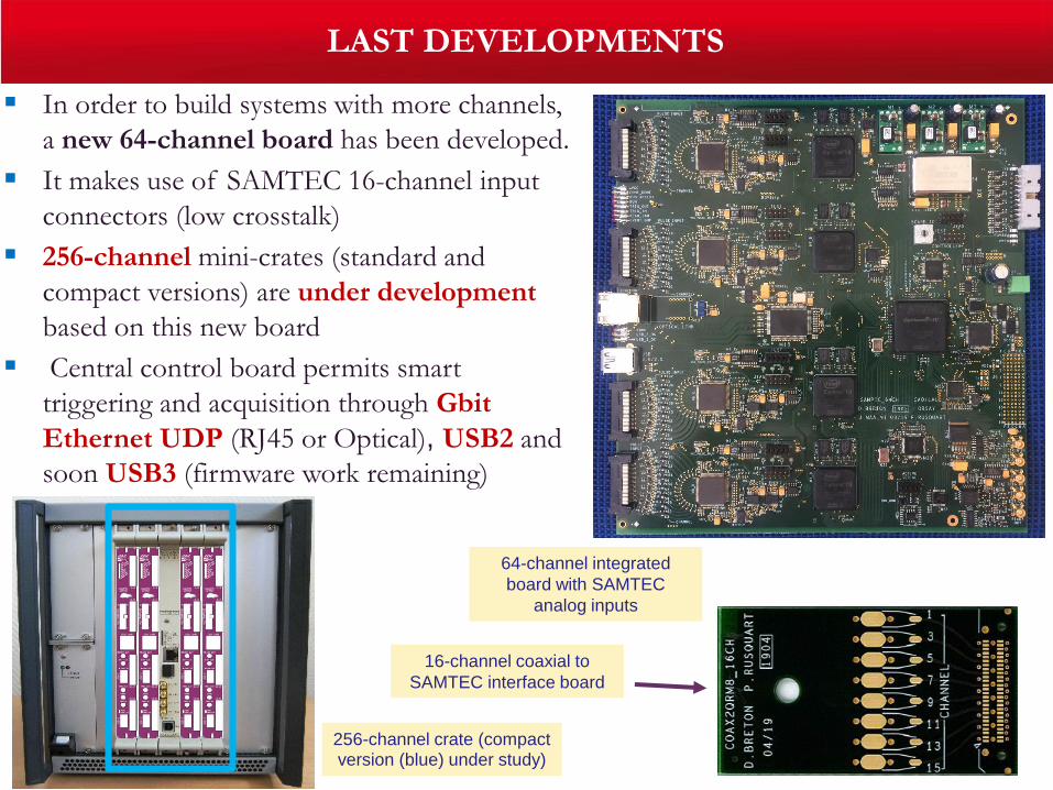
LAST DEVELOPMENTS
In order to build systems with more channels,
a new 64-channel board has been developed.
It makes use of SAMTEC 16-channel input
connectors (low crosstalk)
256-channel mini-crates (standard and
compact versions) are under development
based on this new board
Central control board permits smart
triggering and acquisition through Gbit
Ethernet UDP (RJ45 or Optical), USB2 and
soon USB3 (firmware work remaining)
16-channel coaxial to
SAMTEC interface board
64-channel integrated
board with SAMTEC
analog inputs
256-channel crate (compact version (blue) under study)
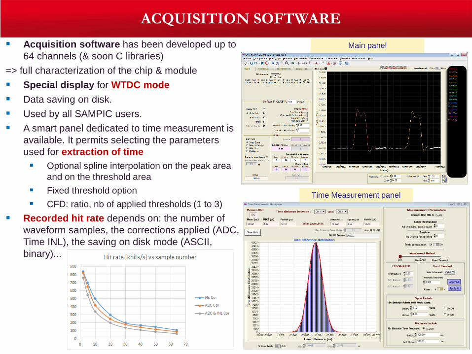
ACQUISITION SOFTWARE
The SAMPIC0
16-channel
mezzanine
Acquisition software has been developed up to
64 channels (& soon C libraries)
=> full characterization of the chip & module
Special display for WTDC mode
Data saving on disk.
Used by all SAMPIC users.
A smart panel dedicated to time measurement is
available. It permits selecting the parameters
used for extraction of time
Optional spline interpolation on the peak area
and on the threshold area
Fixed threshold option
CFD: ratio, nb of applied thresholds (1 to 3)
Recorded hit rate depends on: the number of
waveform samples, the corrections applied (ADC,
Time INL), the saving on disk mode (ASCII,
binary)...
Main panel
Time Measurement panel
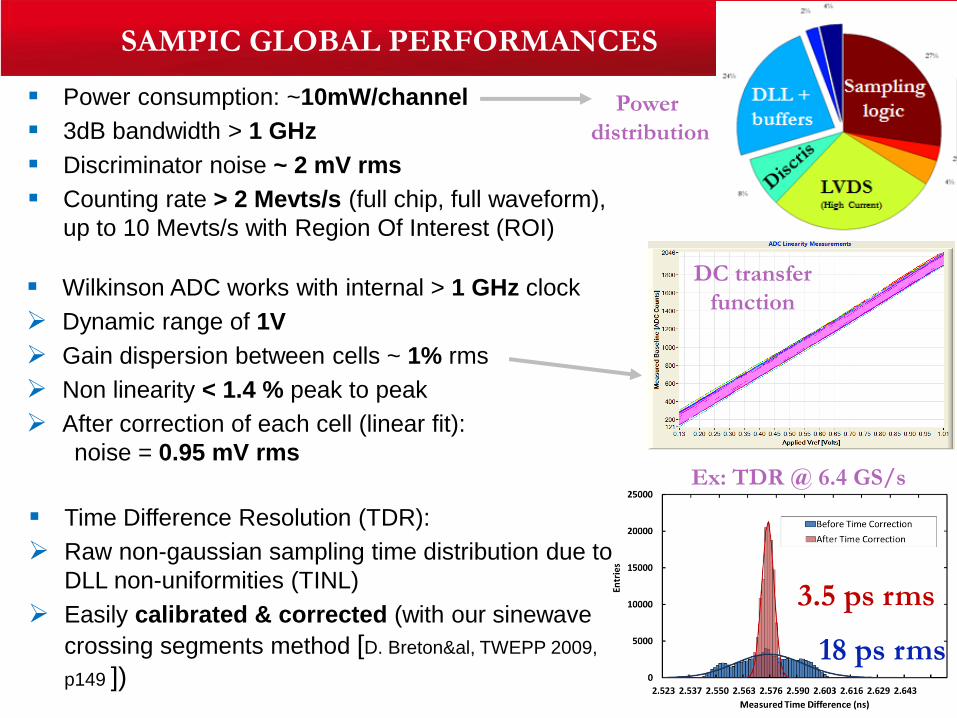
SAMPIC GLOBAL PERFORMANCES
Wilkinson ADC works with internal > 1 GHz clock
Dynamic range of 1V
Gain dispersion between cells ~ 1% rms
Non linearity < 1.4 % peak to peak
After correction of each cell (linear fit):
noise = 0.95 mV rms
DC transfer
function
Power consumption: ~10mW/channel
3dB bandwidth > 1 GHz
Discriminator noise ~ 2 mV rms
Counting rate > 2 Mevts/s (full chip, full waveform),
up to 10 Mevts/s with Region Of Interest (ROI)
Power
distribution
Time Difference Resolution (TDR):
Raw non-gaussian sampling time distribution due to
DLL non-uniformities (TINL)
Easily calibrated & corrected (with our sinewave
crossing segments method [D. Breton&al, TWEPP 2009,
p149 ])18 ps rms
3.5 ps rms
Ex: TDR @ 6.4 GS/s
+_
LVDS to CMOSVin
Vref
Vreset
Polarity
« Timing INL » calib
N_En_translator
En_Diff
En_INL_Calib
En_Channel
En_Diff
1 => ON0 => OFF
En
One pair per channel
En_translator
InternalDAC
En_DAC_Calib
En_Channel
10
Memory cell
En_DAC_Calib
Buffer
Common to all channels
DC supply: V_high or VDD0.6V < V_high < 0.9V
DC supply: V_low or GND0.1V <V_low < 0.4V
Oscillator80, 160 or 320MHz
X 64
Channel
fallingSlopeTune<2:0>
risingSlopeTune<2:0>
Leveltranslator
V_low<2:0>
V_high<2:0>
Analog/Digital
Analog/Digital
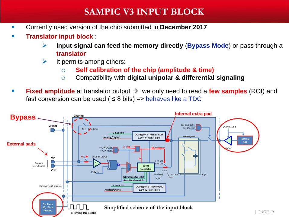
Currently used version of the chip submitted in December 2017
Translator input block :
Input signal can feed the memory directly (Bypass Mode) or pass through a
translator
It permits among others:
o Self calibration of the chip (amplitude & time)
o Compatibility with digital unipolar & differential signaling
Fixed amplitude at translator output we only need to read a few samples (ROI) and
fast conversion can be used ( ≤ 8 bits) => behaves like a TDC
SAMPIC V3 INPUT BLOCK
| PAGE 19Simplified scheme of the input block
BypassInternal extra pad
External pads
| PAGE 20
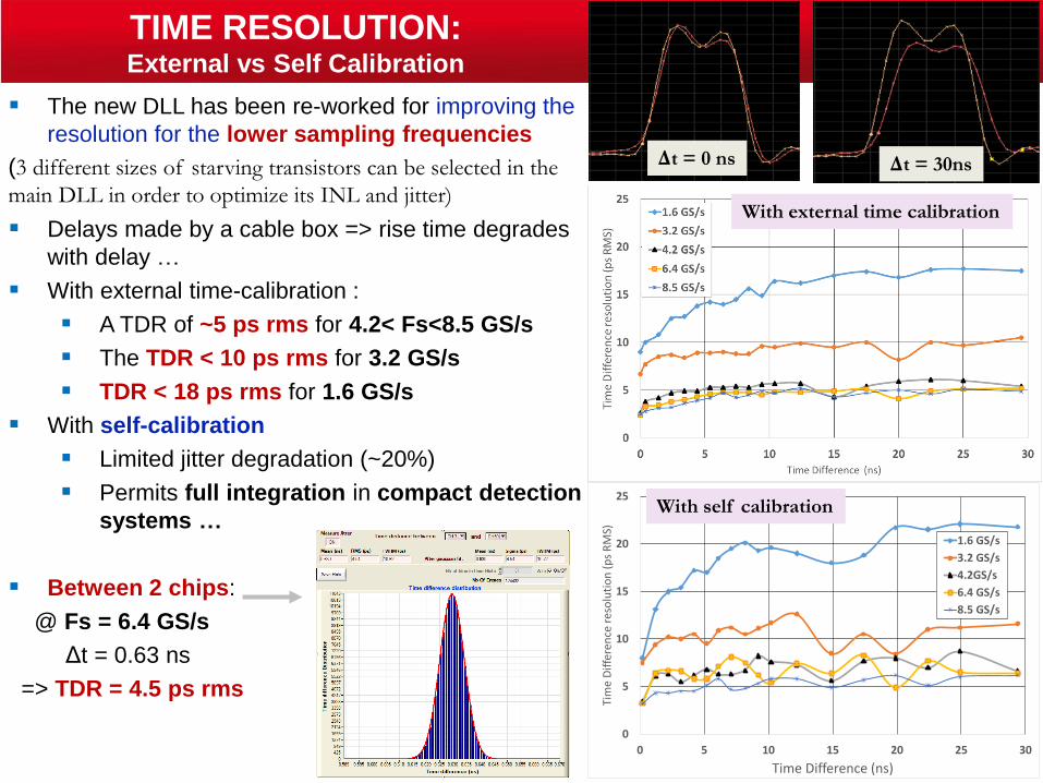
TIME RESOLUTION: External vs Self Calibration
The new DLL has been re-worked for improving the
resolution for the lower sampling frequencies
(3 different sizes of starving transistors can be selected in the
main DLL in order to optimize its INL and jitter)
Delays made by a cable box => rise time degrades
with delay …
With external time-calibration :
A TDR of ~5 ps rms for 4.2< Fs<8.5 GS/s
The TDR < 10 ps rms for 3.2 GS/s
TDR < 18 ps rms for 1.6 GS/s
With self-calibration
Limited jitter degradation (~20%)
Permits full integration in compact detection
systems …
Between 2 chips:
@ Fs = 6.4 GS/s
Δt = 0.63 ns
=> TDR = 4.5 ps rms
0
5
10
15
20
25
0 5 10 15 20 25 30
Tim
e D
iffe
ren
ce r
eso
luti
on
(p
s R
MS)
Time Difference (ns)
1.6 GS/s
3.2 GS/s
4.2GS/s
6.4 GS/s
8.5 GS/s
With external time calibration
With self calibration
Δt = 0 ns Δt = 30ns
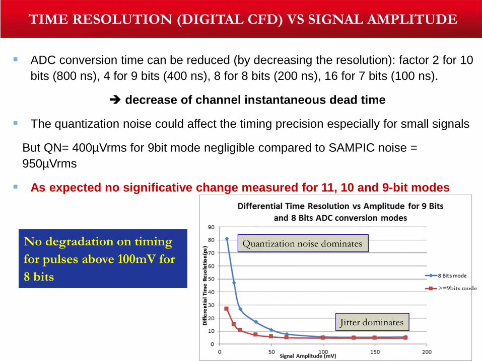
ADC conversion time can be reduced (by decreasing the resolution): factor 2 for 10
bits (800 ns), 4 for 9 bits (400 ns), 8 for 8 bits (200 ns), 16 for 7 bits (100 ns).
decrease of channel instantaneous dead time
The quantization noise could affect the timing precision especially for small signals
But QN= 400µVrms for 9bit mode negligible compared to SAMPIC noise =
950µVrms
As expected no significative change measured for 11, 10 and 9-bit modes
TIME RESOLUTION (DIGITAL CFD) VS SIGNAL AMPLITUDE
No degradation on timing
for pulses above 100mV for
8 bits
NEED FOR EVENT FILTERING…
| PAGE 22
• Whatever the application, it is mandatory to find ways to reject the wrong events as early as
possible in the readout chain in order to keep the dataflow at a reasonable level.
• Like a standard TDC, the Waveform TDC is natively self-triggered on each of its channels.
This may produce very large hit rates, which may cause a saturation of the output buffers,
especially since the waveforms have to be extracted (partially or in totality) together with the
time information.
• In order to reduce the dataflow, it is necessary to filter the good events before conversion. A
central trigger located in the ASIC can then help defining trigger conditions and drastically
reducing the hit rate.
• Moreover, providing the adequate signals out of the chip permits performing in the
surrounding FPGAs a second level trigger based on smarter detector conditions and
increasing the counting noise rejection by a huge factor.
• Noise filters can also be based on the characteristics of the signals as produced by the
different detectors. For instance, a real time filter based on the TOT has been implemented
in SAMPIC. When used with signals issued from crystals and SiPMs, it permits rejecting
above 99% of the dark count noise from the SiPMs.
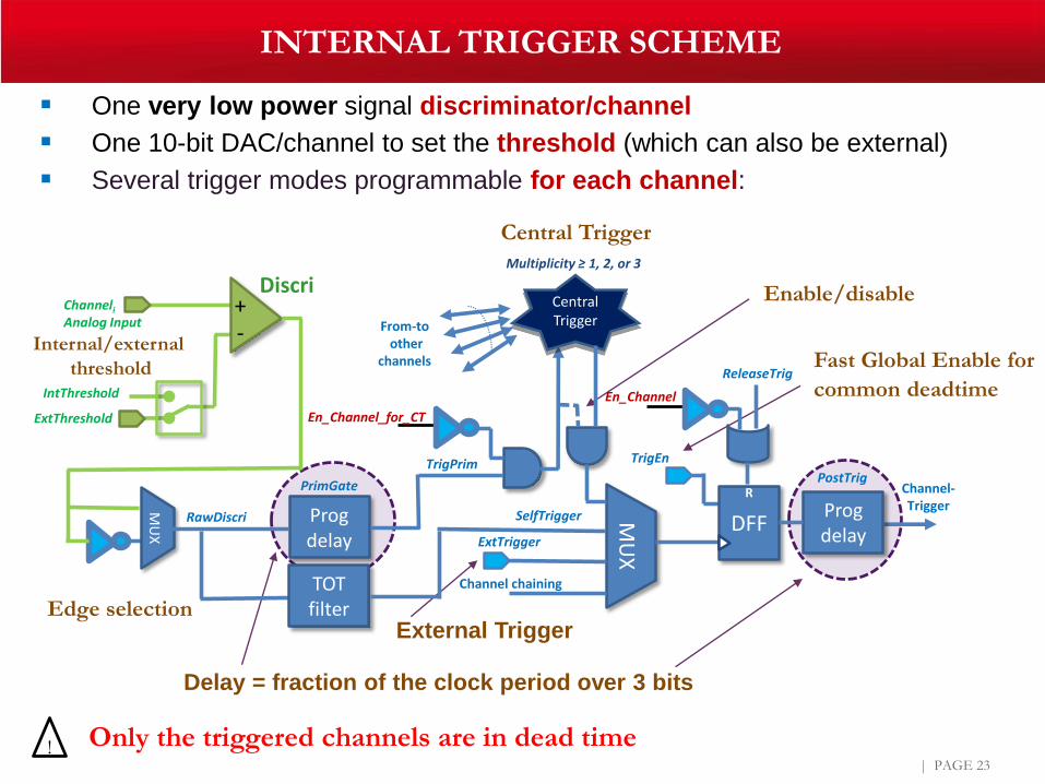
One very low power signal discriminator/channel
One 10-bit DAC/channel to set the threshold (which can also be external)
Several trigger modes programmable for each channel:
INTERNAL TRIGGER SCHEME
| PAGE 23
Only the triggered channels are in dead time
Fast Global Enable for
common deadtime
Edge selection
Internal/external
threshold
Delay = fraction of the clock period over 3 bits
Central Trigger
Enable/disable
External Trigger
!
ExtThreshold
ExtTrigger
MU
X
Channeli
Analog Input
MU
X
Central TriggerFrom-to
otherchannels
TrigEn
Channel-Trigger
DFF
R
Discri
ReleaseTrig
+-
Progdelay
Progdelay
TrigPrim
PrimGatePostTrig
RawDiscri SelfTrigger
En_ChannelIntThreshold
En_Channel_for_CT
Multiplicity ≥ 1, 2, or 3
Channel chainingTOTfilter
TRIGGER PANEL IN THE DAQ SOFTWARE
| PAGE 24
Advanced PingPong Mode
2nd Level Coincidence Mode:
(Two options available)
Coincidence Gate
Central Trigger
Converting channels only
if participating to Central Trigger
Individual channel
trigger modes
Multiplicity
Select channel
that participate to
Central Trigger
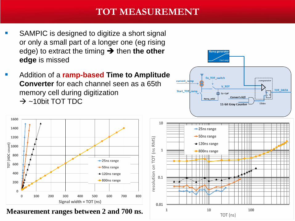
SAMPIC is designed to digitize a short signal
or only a small part of a longer one (eg rising
edge) to extract the timing then the other
edge is missed
Addition of a ramp-based Time to Amplitude
Converter for each channel seen as a 65th
memory cell during digitization
~10bit TOT TDC
TOT MEASUREMENT
| PAGE 25Measurement ranges between 2 and 700 ns.
SUMMARY OF MAIN FEATURES OF SAMPIC V3
| PAGE 26
Smart “central trigger” (OR, multiplicity of 2 & 3) with possibility of common
deadtime or selecting only channels participating in decision
8-step full window PostTrig (very useful for low frequencies)
Channel chaining option: user-defined sets of channels can be chained in time.
“Ping-Pong” (toggling) mode: channels work in pairs.
Integrated TOT measurement and trigger filter based on TOT
All DACs necessary for controlling the chip have been integrated
ADC resolution internally selectable between 7 and 11 bits
Auto-conversion mode for ADC: the conversion can be automatically started
when an event is detected, independently for each channel.
Reduce the required external digital electronics
But the handshake mode with the FPGA permits building a 2nd Level
trigger based on many chips for a common event selection
Auto-calibration (Time INL): dedicated signal sources are implemented in the
chip in order to perform time INL calibrations in standalone.
• SAMPIC modules are already used with different detectors on test benches or
test beams. A lot of examples were already presented at the WaveCatcher and
SAMPIC Workshop in February 2018 in Orsay (second workshop soon).
• Tested with PMTs, MCP-PMTs, APDs, SiPMs, fast Silicon Detectors,
Diamonds: performances are equivalent to those with high-end oscilloscopes
Different R&Ds ongoing with the TOF-PET community (CERN, IRFU, USA…)
SAMPIC has been used for many test beams at CERN
TOTEM has developed a CMS-compatible motherboard housing SAMPIC
mezzanines. 192 measurement channels are in use on the LHC.
SAMPIC is the baseline readout option for the Fast Timing Detector, the
Surround Background Tagger and the Muon Detector of the SHIP collaboration.
Used for the readout of the new LiquidO detector R&D concept
Used for T2K near detector Upgrade: 256-channel Timing Detector.
Used by Photek for characterization of new ultra-fast MCP-PMTs (IEEE paper)
KU recently ordered 2 modules for satellites test benches at NASA .
TAKING DATA WITH DETECTORS
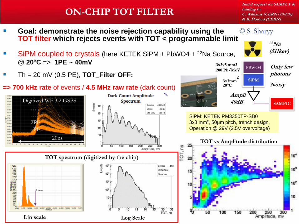
Goal: demonstrate the noise rejection capability using the TOT filter which rejects events with TOT < programmable limit
SiPM coupled to crystals (here KETEK SiPM + PbWO4 + 22Na Source,
@ 20°C => 1PE ~ 40mV
Th = 20 mV (0.5 PE), TOT_Filter OFF:
=> 700 kHz rate of events / 4.5 MHz raw rate (dark count)
ON-CHIP TOT FILTER
SiPM: KETEK PM3350TP-SB0
3x3 mm², 50μm pitch, trench design,
Operation @ 29V (2.5V overvoltage)
PBWO4
SiPMNoisy
Only few photons
22Na (511kev)
Ampli40dB SAMPIC
Digitized WF 3.2 GSPS
…
…
2PE
1PE
20ns
TOT spectrum (digitized by the chip)
15ns
3x3mm2
20°C
3x3x5 mm3
200 Ph/MeV
© S. Sharyy
Lin scale Log Scale
TOT vs Amplitude distribution
Initial request for SAMPET & funding byC. Williams (CERN+INFN) & K. Doroud (CERN)
| PAGE 29
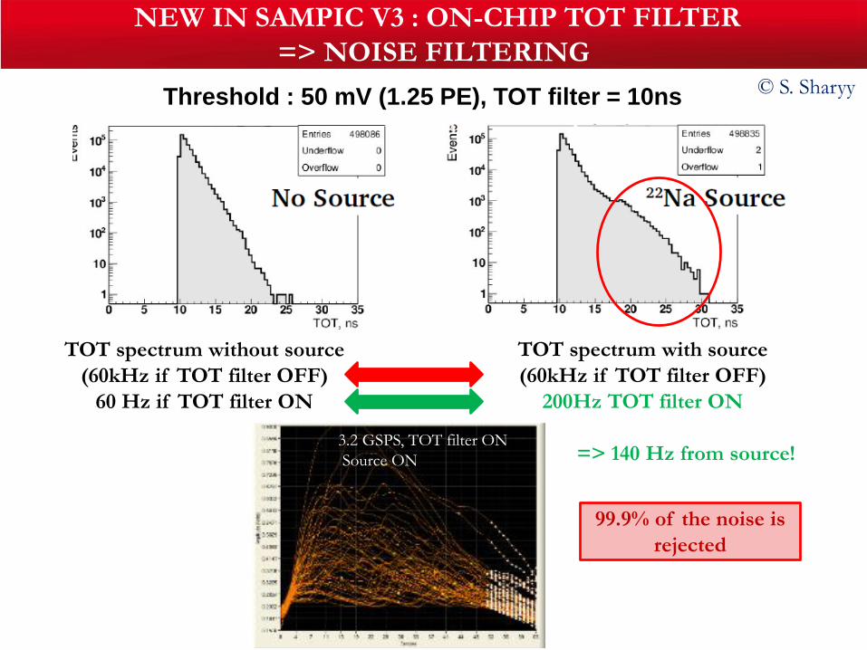
20ns
3.2 GSPS, TOT filter ON
Source ON
TOT spectrum without source
(60kHz if TOT filter OFF)
60 Hz if TOT filter ON
TOT spectrum with source
(60kHz if TOT filter OFF)
200Hz TOT filter ON
=> 140 Hz from source!
Threshold : 50 mV (1.25 PE), TOT filter = 10ns
NEW IN SAMPIC V3 : ON-CHIP TOT FILTER
=> NOISE FILTERING© S. Sharyy
99.9% of the noise is
rejected
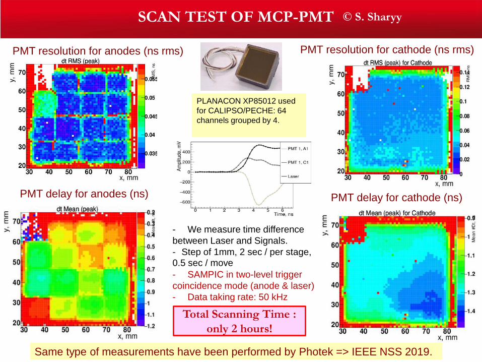
SCAN TEST OF MCP-PMT
PMT resolution for anodes (ns rms)
PMT delay for anodes (ns)
PMT resolution for cathode (ns rms)
PMT delay for cathode (ns)
© S. Sharyy
- We measure time difference
between Laser and Signals.
- Step of 1mm, 2 sec / per stage, 0.5 sec / move
- SAMPIC in two-level trigger
coincidence mode (anode & laser)
- Data taking rate: 50 kHz
PLANACON XP85012 used
for CALIPSO/PECHE: 64
channels grouped by 4.
Total Scanning Time :
only 2 hours!
Same type of measurements have been performed by Photek => IEEE NSS 2019.
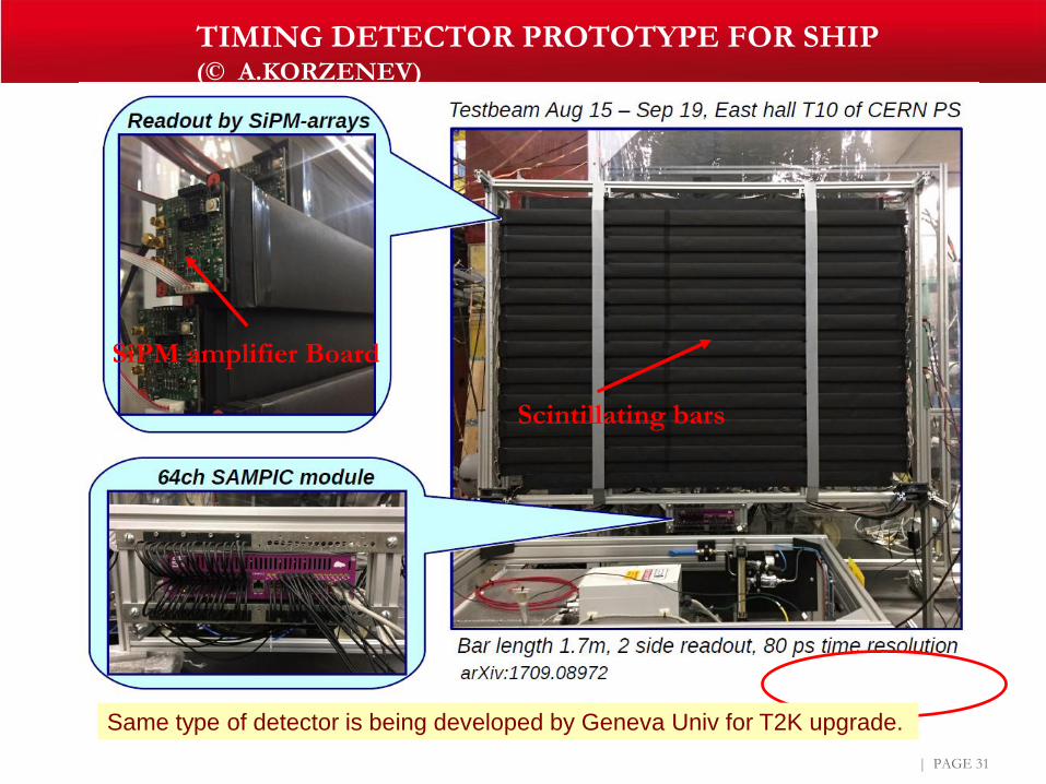
TIMING DETECTOR PROTOTYPE FOR SHIP(© A.KORZENEV)
| PAGE 31
Scintillating bars
SiPM amplifier Board
Same type of detector is being developed by Geneva Univ for T2K upgrade.
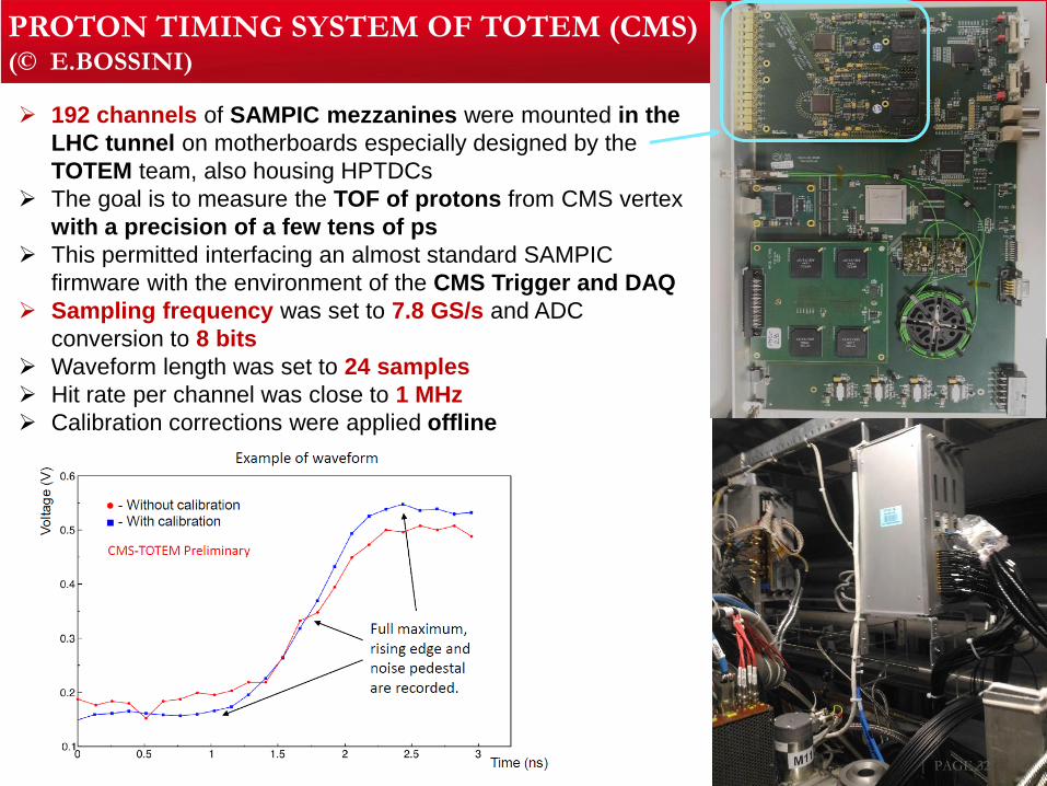
PROTON TIMING SYSTEM OF TOTEM (CMS)(© E.BOSSINI)
| PAGE 32
192 channels of SAMPIC mezzanines were mounted in the
LHC tunnel on motherboards especially designed by the
TOTEM team, also housing HPTDCs
The goal is to measure the TOF of protons from CMS vertex
with a precision of a few tens of ps
This permitted interfacing an almost standard SAMPIC
firmware with the environment of the CMS Trigger and DAQ
Sampling frequency was set to 7.8 GS/s and ADC
conversion to 8 bits
Waveform length was set to 24 samples
Hit rate per channel was close to 1 MHz
Calibration corrections were applied offline
| PAGE 33
• The main challenges when developing electronics systems for ps level measurement are the
following:
• High quality of the clock distribution.
• Electronics noise which translates into jitter => signal over Noise Ratio has to be as
high as possible.
• Analog crosstalk between channels which introduces bias for timing. This is true
mostly for neighboring channels receiving signal at the same time, which has to be
avoided if possible.
• Time INL of the DLL’s driving the sampling. This INL must be calibrated properly, if
possible on-detector, and correction can be applied offline.
• Analog to digital conversion has to be as fast as possible to reduce dead-time.
• Adequate triggering conditions for counting noise rejection in order to avoid
saturating the dataflow.
• In the case of large systems, high channel density requiring a very compact and low
power acquisition chain.
MAIN CHALLENGES FOR PS MEASUREMENT
| PAGE 34
• In summary, signal waveform obviously contains the full information.
• Fast timing means large analog signal bandwidth and high sampling rates but this
induces huge dataflow levels.
• A key is to try keeping only the good information.
• In the case of high-end oscilloscopes, trigger is performed on digital data thus the use
of fast ADCs is mandatory. But their cost limits their use to a few channels.
• “Standard” analog memories nicely replace ADCs in most cases, but dead-time
remains their main limitation at high rates.
• This is not the case of TDCs but they do not provide the signal shape.
• The Waveform TDC seems to be an adequate compromise in face of all these
constraints, especially associated to smart trigger configurations.
• Time measurement at a few tens ps level is becoming a way for high energy physics
experiments to face extremely high luminosity levels. There, the hit rates (>> MHz per
channel) associated with the channel densities impose new challenges for waveform
sampling and real time feature extraction.
• New architectures are being imagined, taking benefit of the knowledge of the particle
arrival time when used on colliders.
SUMMARY
| PAGE 35
SAMPIC is a full System On Chip:
• Analog or digital input, fully digital output
• All the DACs and calibration generators are integrated
• It just requires power, clock, and a simple interface with an FPGA
• Small power consumption ~10 mW/channel
• All the channels can be fully independent
• Raw counting rate can go >> 100 kHz/ch.
• Large choice of smart triggers
It can be used for a highly integrated tiny module (cm³) as well as for large scale
detectors (nuclear or high energy physics, TOF-PETs, …).
A slower version is under study for nuclear physics => ~200 MS/s to ~1 GS/s
Many types of modules have been developed: 16 to 256-channel modules.
Ongoing licensing with CAEN.
End of AMS 0,18 µm => migrated to TSI 0.18µm (also sourced from IBM 0.18µm)
For more information:
http://wpsist.lal.in2p3.fr/wasiw2018/
CONCLUSION ABOUT SAMPIC
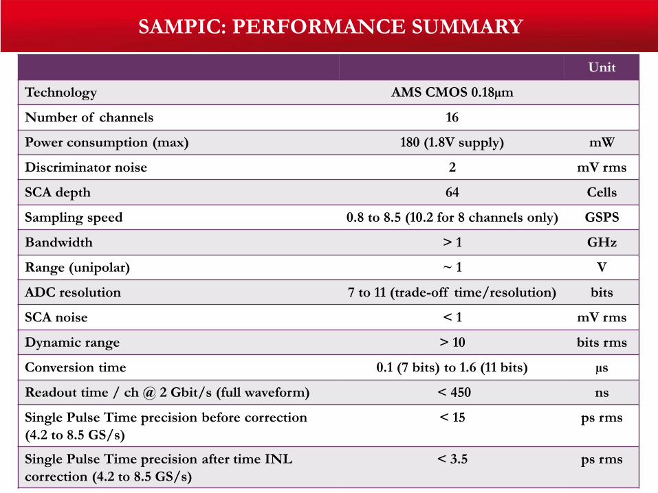
SAMPIC: PERFORMANCE SUMMARY
| PAGE 36
Unit
Technology AMS CMOS 0.18µm
Number of channels 16
Power consumption (max) 180 (1.8V supply) mW
Discriminator noise 2 mV rms
SCA depth 64 Cells
Sampling speed 0.8 to 8.5 (10.2 for 8 channels only) GSPS
Bandwidth > 1 GHz
Range (unipolar) ~ 1 V
ADC resolution 7 to 11 (trade-off time/resolution) bits
SCA noise < 1 mV rms
Dynamic range > 10 bits rms
Conversion time 0.1 (7 bits) to 1.6 (11 bits) µs
Readout time / ch @ 2 Gbit/s (full waveform) < 450 ns
Single Pulse Time precision before correction
(4.2 to 8.5 GS/s)
< 15 ps rms
Single Pulse Time precision after time INL
correction (4.2 to 8.5 GS/s)
< 3.5 ps rms

BACKUP SLIDES
| PAGE 37
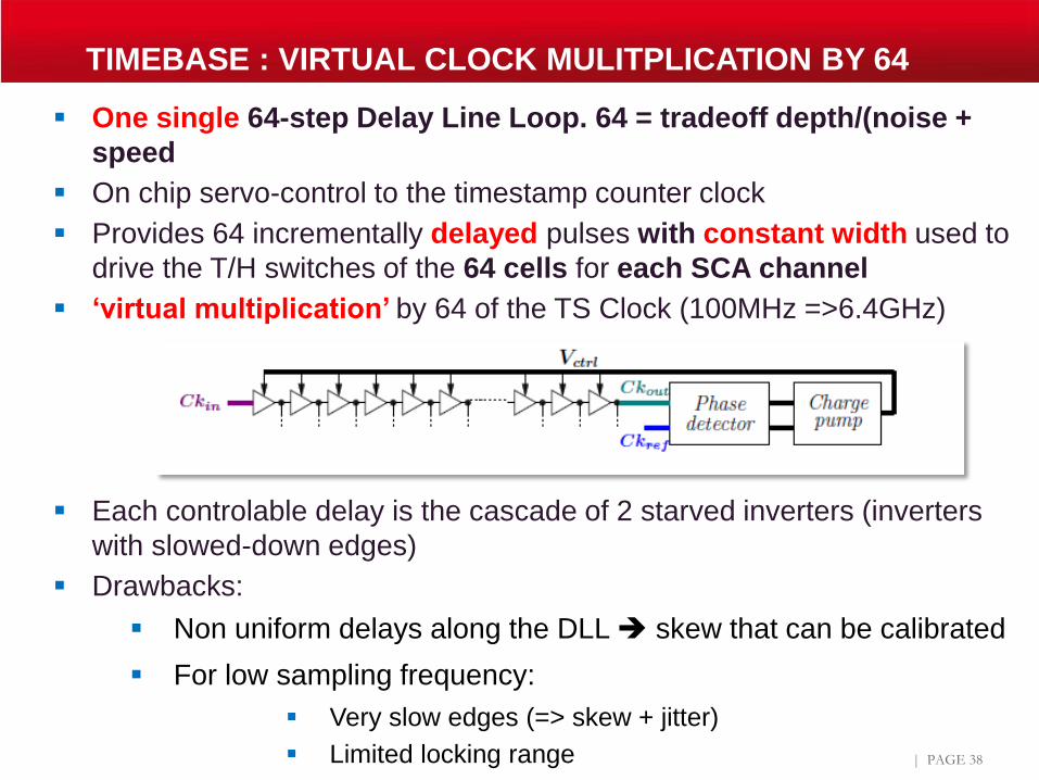
TIMEBASE : VIRTUAL CLOCK MULITPLICATION BY 64
One single 64-step Delay Line Loop. 64 = tradeoff depth/(noise +
speed
On chip servo-control to the timestamp counter clock
Provides 64 incrementally delayed pulses with constant width used to
drive the T/H switches of the 64 cells for each SCA channel
‘virtual multiplication’ by 64 of the TS Clock (100MHz =>6.4GHz)
Each controlable delay is the cascade of 2 starved inverters (inverters
with slowed-down edges)
Drawbacks:
Non uniform delays along the DLL skew that can be calibrated
For low sampling frequency:
Very slow edges (=> skew + jitter)
Limited locking range | PAGE 38
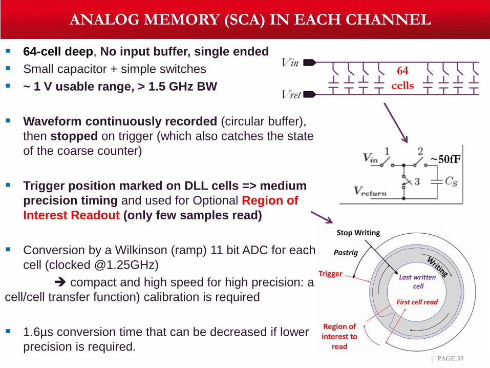
64-cell deep, No input buffer, single ended
Small capacitor + simple switches
~ 1 V usable range, > 1.5 GHz BW
Waveform continuously recorded (circular buffer),
then stopped on trigger (which also catches the state
of the coarse counter)
Trigger position marked on DLL cells => medium
precision timing and used for Optional Region of
Interest Readout (only few samples read)
Conversion by a Wilkinson (ramp) 11 bit ADC for each
cell (clocked @1.25GHz)
compact and high speed for high precision: a
cell/cell transfer function) calibration is required
1.6µs conversion time that can be decreased if lower
precision is required.
ANALOG MEMORY (SCA) IN EACH CHANNEL
| PAGE 39
~50fF
64
cells
Vin
Vret
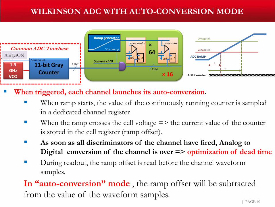
WILKINSON ADC WITH AUTO-CONVERSION MODE
| PAGE 40
When triggered, each channel launches its auto-conversion.
When ramp starts, the value of the continuously running counter is sampled
in a dedicated channel register
When the ramp crosses the cell voltage => the current value of the counter
is stored in the cell register (ramp offset).
As soon as all discriminators of the channel have fired, Analog to
Digital conversion of the channel is over => optimization of dead time
During readout, the ramp offset is read before the channel waveform
samples.
In “auto-conversion” mode , the ramp offset will be subtracted
from the value of the waveform samples.
Common ADC TimebaseAlwaysON
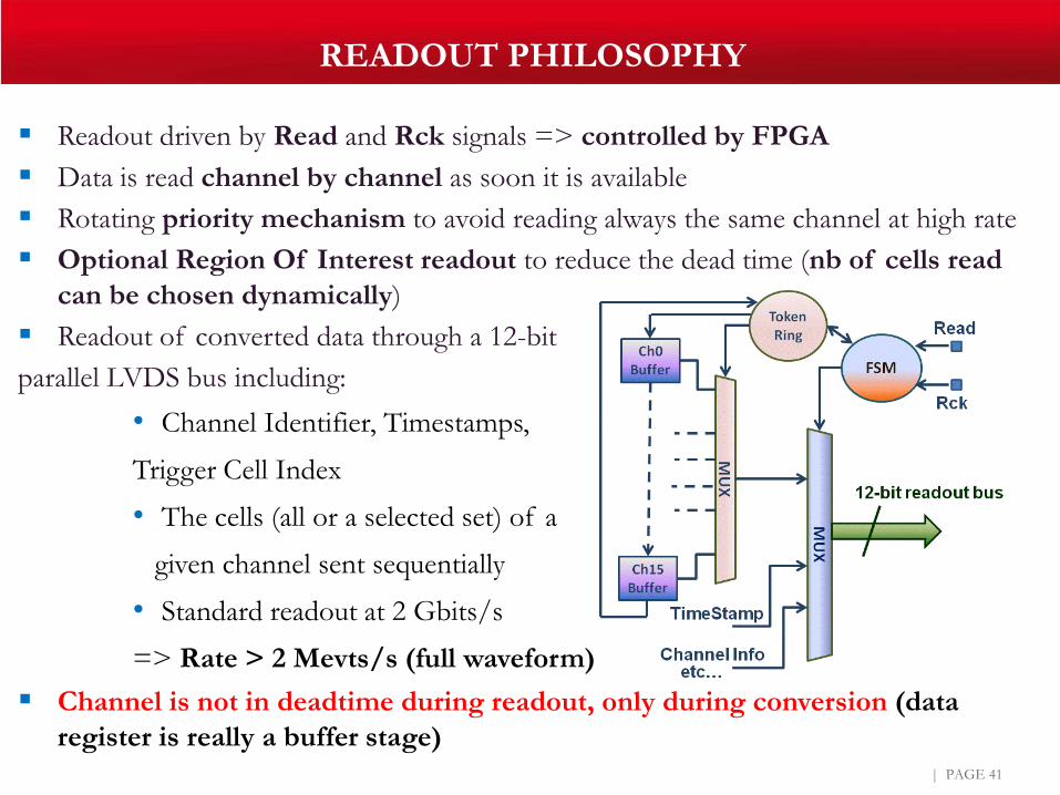
Readout driven by Read and Rck signals => controlled by FPGA
Data is read channel by channel as soon it is available
Rotating priority mechanism to avoid reading always the same channel at high rate
Optional Region Of Interest readout to reduce the dead time (nb of cells read
can be chosen dynamically)
Readout of converted data through a 12-bit
parallel LVDS bus including:
• Channel Identifier, Timestamps,
Trigger Cell Index
• The cells (all or a selected set) of a
given channel sent sequentially
• Standard readout at 2 Gbits/s
=> Rate > 2 Mevts/s (full waveform)
Channel is not in deadtime during readout, only during conversion (data
register is really a buffer stage)
READOUT PHILOSOPHY
| PAGE 41
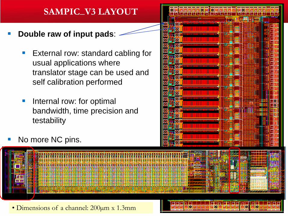
Double raw of input pads:
External row: standard cabling for
usual applications where
translator stage can be used and
self calibration performed
Internal row: for optimal
bandwidth, time precision and
testability
No more NC pins.
| PAGE 42
SAMPIC_V3 LAYOUT
• Dimensions of a channel: 200µm x 1.3mm
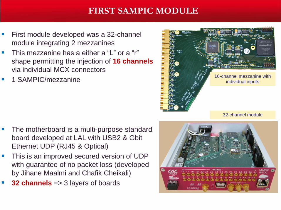
First module developed was a 32-channel
module integrating 2 mezzanines
This mezzanine has a either a “L” or a “r”
shape permitting the injection of 16 channels
via individual MCX connectors
1 SAMPIC/mezzanine
The motherboard is a multi-purpose standard
board developed at LAL with USB2 & Gbit
Ethernet UDP (RJ45 & Optical)
This is an improved secured version of UDP
with guarantee of no packet loss (developed
by Jihane Maalmi and Chafik Cheikali)
32 channels => 3 layers of boards
32-channel module
16-channel mezzanine withindividual inputs
FIRST SAMPIC MODULE
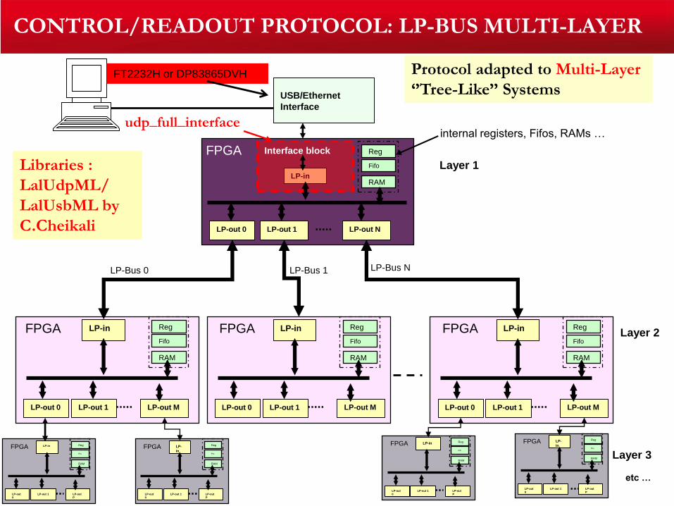
LP-out 0
LP-in
FPGA Interface block
LP-out 1 LP-out N
Reg
Fifo
RAM
CONTROL/READOUT PROTOCOL: LP-BUS MULTI-LAYER
Protocol adapted to Multi-Layer
‘’Tree-Like’’ Systems
udp_full_interface
Libraries :
LalUdpML/
LalUsbML by
C.Cheikali
LP-out 0
LP-inFPGA
LP-out 1 LP-out M
Reg
Fifo
RAM
LP-out 0
LP-inFPGA
LP-out 1 LP-out M
Reg
Fifo
RAM
Layer 2
USB/Ethernet
Interface
Layer 1
Layer 3
etc …
FT2232H or DP83865DVH
LP-Bus 0 LP-Bus 1 LP-Bus N
LP-out 0
LP-inFPGA
LP-out 1 LP-out M
Reg
Fifo
RAM
LP-out
0
LP-inFPGA
LP-out 1 LP-out
P
Reg
Fifo
RAM
LP-out
0
LP-
inFPGA
LP-out 1 LP-out
P
Reg
Fifo
RAM
LP-out
0
LP-inFPGA
LP-out 1 LP-out
P
Reg
Fifo
RAM
LP-out
0
LP-
inFPGA
LP-out 1 LP-out
P
Reg
Fifo
RAM
internal registers, Fifos, RAMs …
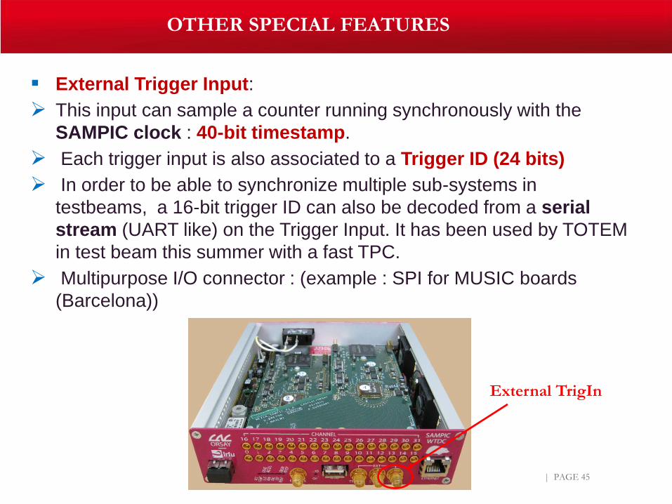
External Trigger Input:
This input can sample a counter running synchronously with the
SAMPIC clock : 40-bit timestamp.
Each trigger input is also associated to a Trigger ID (24 bits)
In order to be able to synchronize multiple sub-systems in
testbeams, a 16-bit trigger ID can also be decoded from a serial
stream (UART like) on the Trigger Input. It has been used by TOTEM
in test beam this summer with a fast TPC.
Multipurpose I/O connector : (example : SPI for MUSIC boards
(Barcelona))
OTHER SPECIAL FEATURES
| PAGE 45
External TrigIn
TEK MSO71604C
(16GHz BW, 100GSPS)
1ns /divtr = 386ps
SAMPIC BYPASS
8.5 GSPS
(first raw of pads)
tr ~ 400ps
SAMPIC classic 8.5 GSPS
(second row of pads).
Tr ~ 400ps
SAMPIC Bypass
4.2 GSPS
WAVEFORM RESPONSE WITH NEW INPUT
CONFIGURATION
Pulse (~460 mV pp) with sharp edges => compare the response from SAMPIC
and from a 16 GSPS oscilloscope:
Signal produced by a LeCroy 9214 generator.
Permits estimating SAMPIC bypass bandwidth: > 1 GHz
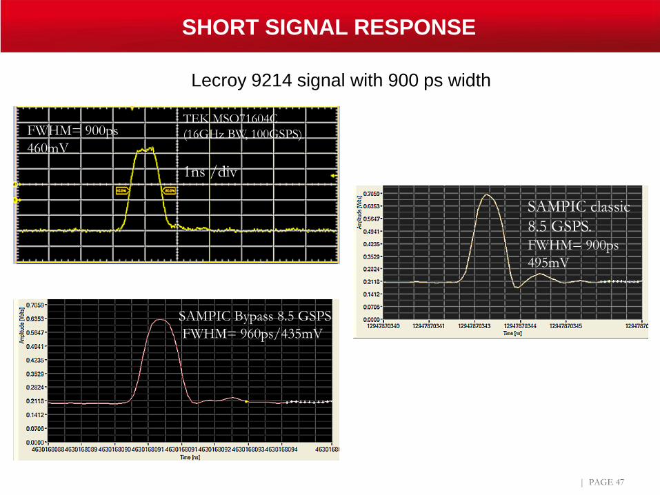
| PAGE 47
TEK MSO71604C
(16GHz BW, 100GSPS)
1ns /div
Lecroy 9214 signal with 900 ps width
SAMPIC Bypass 8.5 GSPS
FWHM= 960ps/435mV
SAMPIC classic
8.5 GSPS. FWHM= 900ps
495mV
FWHM= 900ps
460mV
SHORT SIGNAL RESPONSE
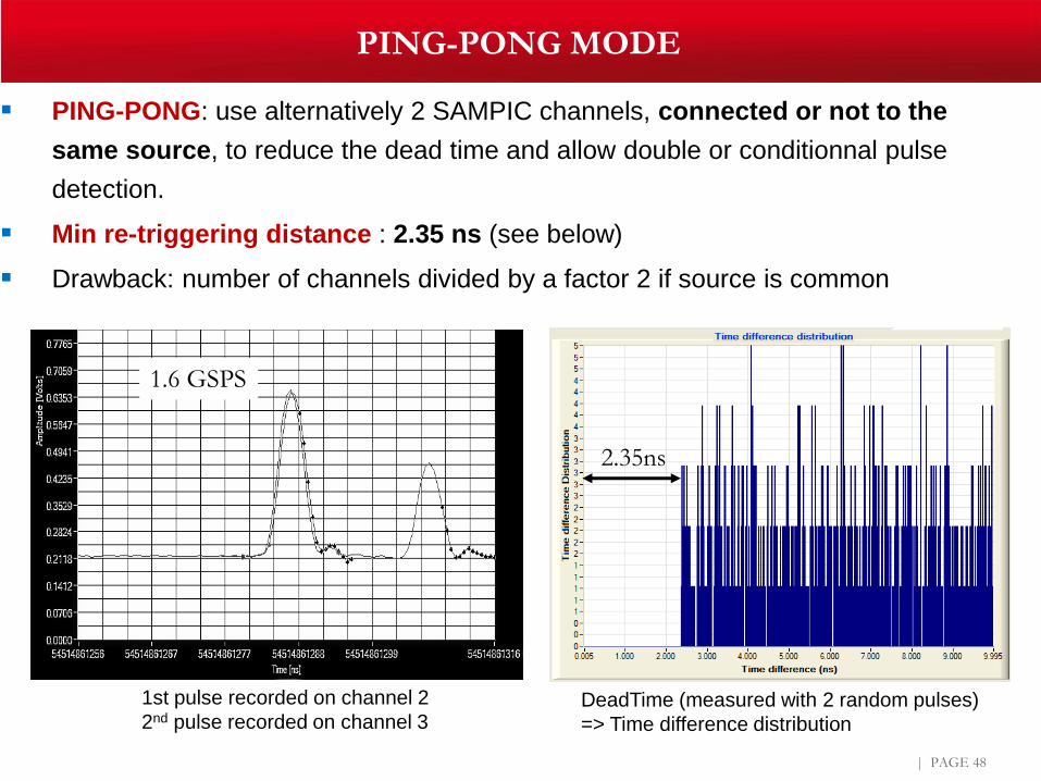
PING-PONG: use alternatively 2 SAMPIC channels, connected or not to the
same source, to reduce the dead time and allow double or conditionnal pulse
detection.
Min re-triggering distance : 2.35 ns (see below)
Drawback: number of channels divided by a factor 2 if source is common
PING-PONG MODE
| PAGE 48
1st pulse recorded on channel 2
2nd pulse recorded on channel 3
1.6 GSPS
DeadTime (measured with 2 random pulses)
=> Time difference distribution
2.35ns
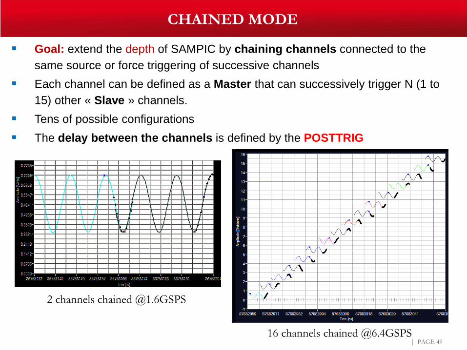
Goal: extend the depth of SAMPIC by chaining channels connected to the
same source or force triggering of successive channels
Each channel can be defined as a Master that can successively trigger N (1 to
15) other « Slave » channels.
Tens of possible configurations
The delay between the channels is defined by the POSTTRIG
CHAINED MODE
| PAGE 49
2 channels chained @1.6GSPS
16 channels chained @6.4GSPS
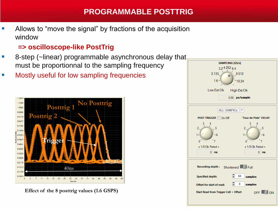
PROGRAMMABLE POSTTRIG
| PAGE 50
Allows to “move the signal” by fractions of the acquisition
window
=> oscilloscope-like PostTrig
8-step (~linear) programmable asynchronous delay that
must be proportionnal to the sampling frequency
Mostly useful for low sampling frequencies
Effect of the 8 posttrig values (1.6 GSPS)
No Posttrig
Trigger
40ns
Posttrig 1
Posttrig 2
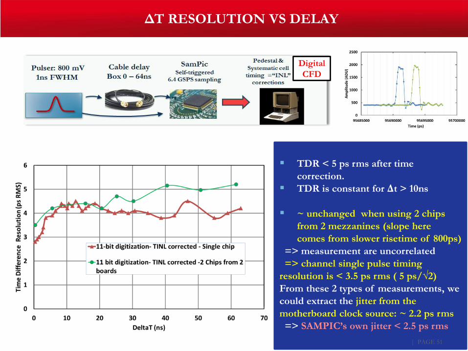
TDR < 5 ps rms after time
correction.
TDR is constant for Δt > 10ns
~ unchanged when using 2 chips
from 2 mezzanines (slope here
comes from slower risetime of 800ps)
=> measurement are uncorrelated
=> channel single pulse timing
resolution is < 3.5 ps rms ( 5 ps/√2)
From these 2 types of measurements, we
could extract the jitter from the
motherboard clock source: ~ 2.2 ps rms
=> SAMPIC’s own jitter < 2.5 ps rms
| PAGE 51
ΔT RESOLUTION VS DELAY
Digital
CFD
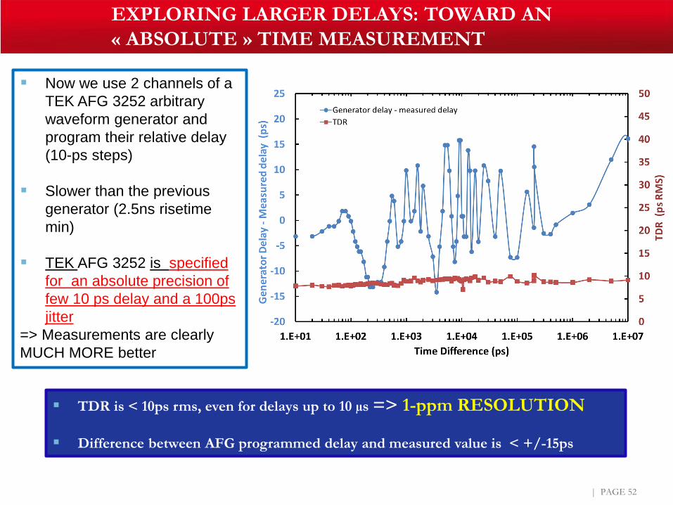
EXPLORING LARGER DELAYS: TOWARD AN
« ABSOLUTE » TIME MEASUREMENT
| PAGE 52
Now we use 2 channels of a
TEK AFG 3252 arbitrary
waveform generator and
program their relative delay
(10-ps steps)
Slower than the previous
generator (2.5ns risetime
min)
TEK AFG 3252 is specified
for an absolute precision of
few 10 ps delay and a 100ps
jitter
=> Measurements are clearly
MUCH MORE better
TDR is < 10ps rms, even for delays up to 10 µs => 1-ppm RESOLUTION
Difference between AFG programmed delay and measured value is < +/-15ps
Periodic pattern (~1ns)
DLL in the AWG ?
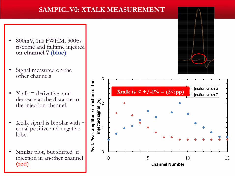
SAMPIC_V0: XTALK MEASUREMENT
• 800mV, 1ns FWHM, 300ps risetime and falltime injected on channel 7 (blue)
• Signal measured on the other channels
• Xtalk = derivative and decrease as the distance to the injection channel
• Xtalk signal is bipolar with ~ equal positive and negative lobe
• Similar plot, but shifted if injection in another channel (red)
Xtalk is < +/-1% = (2%pp)
CALIBRATION PHILOSOPHY
| PAGE 54
SCAs-based chips exhibit reproducible non-idealities which can be easily
corrected after calibration:
The goal is to find the set with the best performance/complexity ratio.
But also to find the right set for the highest level of performance.
SAMPIC actually offers very good performance with only two types of
simple calibrations :
Amplitude: cell pedestal and gain (linear or parabolic fit) => DC ramp
Time: INL (one offset per cell) => use of a simple sinewave (see backup)
This leads to a limited volume of standard calibration data (4 to 6
Bytes/cell/sampling frequency => 5 to 8 kBytes/chip/sampling frequency)
=> can be stored in the on-board EEPROM (1Mbit).
These simple corrections could even be applied in the FPGA.
Highest level calibrations permit debugging the chip and pushing the
performance to its limit (still unknown).
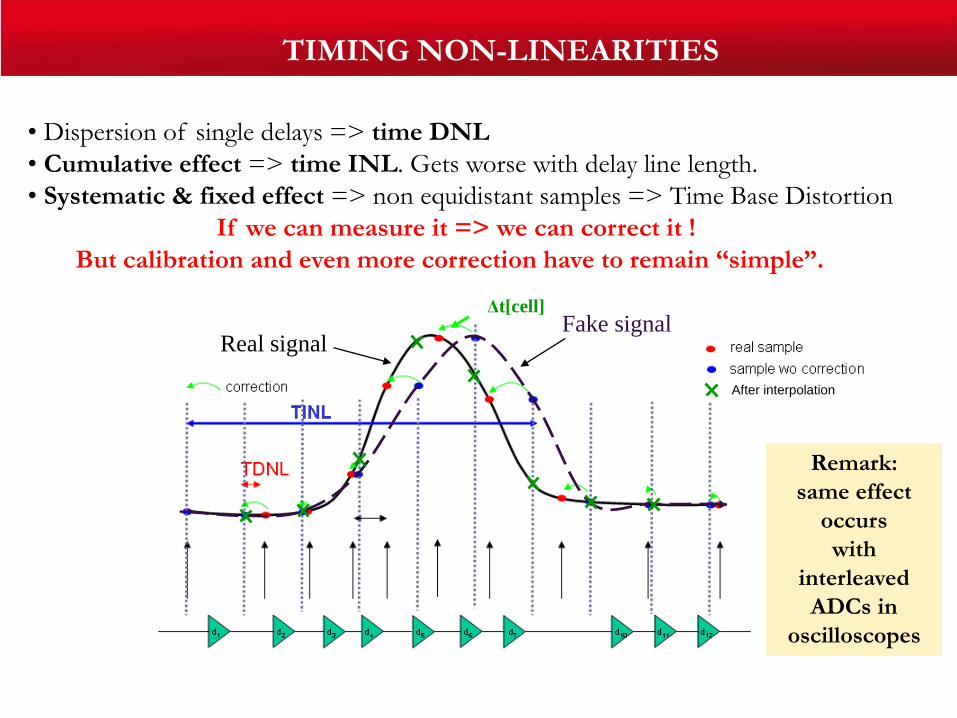
• Dispersion of single delays => time DNL
• Cumulative effect => time INL. Gets worse with delay line length.
• Systematic & fixed effect => non equidistant samples => Time Base Distortion
If we can measure it => we can correct it !
But calibration and even more correction have to remain “simple”.
TIMING NON-LINEARITIES
Real signalFake signal
After interpolation
Δt[cell]
Remark:
same effect
occurs
with
interleaved
ADCs in
oscilloscopes
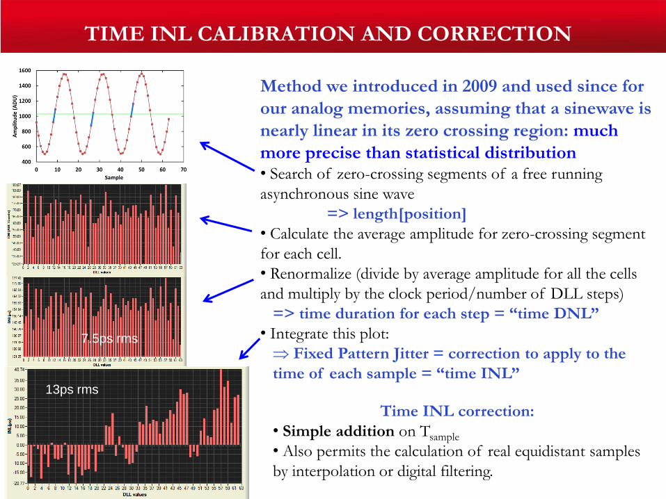
Method we introduced in 2009 and used since for
our analog memories, assuming that a sinewave is
nearly linear in its zero crossing region: much
more precise than statistical distribution• Search of zero-crossing segments of a free running
asynchronous sine wave
=> length[position]
• Calculate the average amplitude for zero-crossing segment
for each cell.
• Renormalize (divide by average amplitude for all the cells
and multiply by the clock period/number of DLL steps)
=> time duration for each step = “time DNL”
• Integrate this plot:
Fixed Pattern Jitter = correction to apply to the
time of each sample = “time INL”
Time INL correction:
• Simple addition on Tsample
• Also permits the calculation of real equidistant samples
by interpolation or digital filtering.
TIME INL CALIBRATION AND CORRECTION
7.5ps rms
13ps rms
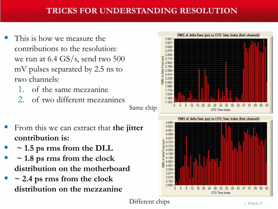
TRICKS FOR UNDERSTANDING RESOLUTION
| PAGE 57
This is how we measure the
contributions to the resolution:
we run at 6.4 GS/s, send two 500
mV pulses separated by 2.5 ns to
two channels:
1. of the same mezzanine
2. of two different mezzanines
From this we can extract that the jitter
contribution is:
~ 1.5 ps rms from the DLL
~ 1.8 ps rms from the clock
distribution on the motherboard
~ 2.4 ps rms from the clock
distribution on the mezzanine
Same chip
Different chips
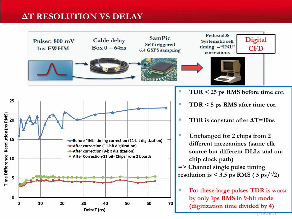
TDR < 25 ps RMS before time cor.
TDR < 5 ps RMS after time cor.
TDR is constant after ΔT=10ns
Unchanged for 2 chips from 2
different mezzanines (same clk
source but different DLLs and on-
chip clock path)
=> Channel single pulse timing
resolution is < 3.5 ps RMS ( 5 ps/√2)
For these large pulses TDR is worst
by only 1ps RMS in 9-bit mode
(digitization time divided by 4)| PAGE 58
ΔT RESOLUTION VS DELAY
Digital
CFD
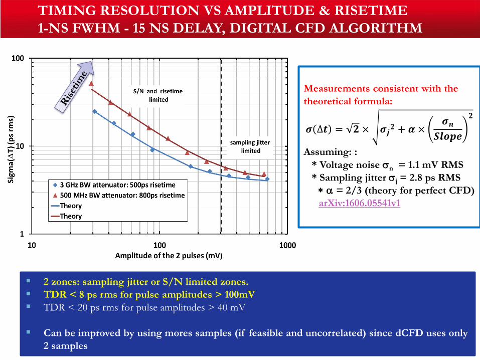
TIMING RESOLUTION VS AMPLITUDE & RISETIME
1-NS FWHM - 15 NS DELAY, DIGITAL CFD ALGORITHM
| PAGE 59
2 zones: sampling jitter or S/N limited zones.
TDR < 8 ps rms for pulse amplitudes > 100mV
TDR < 20 ps rms for pulse amplitudes > 40 mV
Can be improved by using mores samples (if feasible and uncorrelated) since dCFD uses only
2 samples
Measurements consistent with the
theoretical formula:
𝝈 ∆𝒕 = 𝟐 × 𝝈𝒋𝟐 + 𝜶 ×
𝝈𝒏𝑺𝒍𝒐𝒑𝒆
𝟐
Assuming: :
* Voltage noise sn = 1.1 mV RMS
* Sampling jitter sj = 2.8 ps RMS
* a = 2/3 (theory for perfect CFD)
arXiv:1606.05541v1
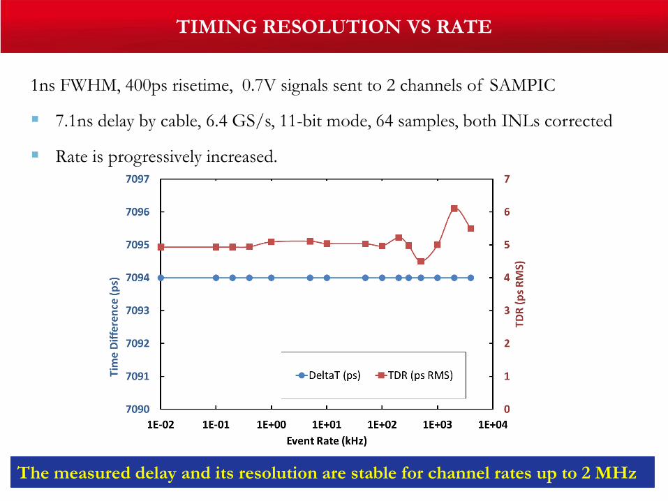
1ns FWHM, 400ps risetime, 0.7V signals sent to 2 channels of SAMPIC
7.1ns delay by cable, 6.4 GS/s, 11-bit mode, 64 samples, both INLs corrected
Rate is progressively increased.
TIMING RESOLUTION VS RATE
The measured delay and its resolution are stable for channel rates up to 2 MHz
| PAGE 61
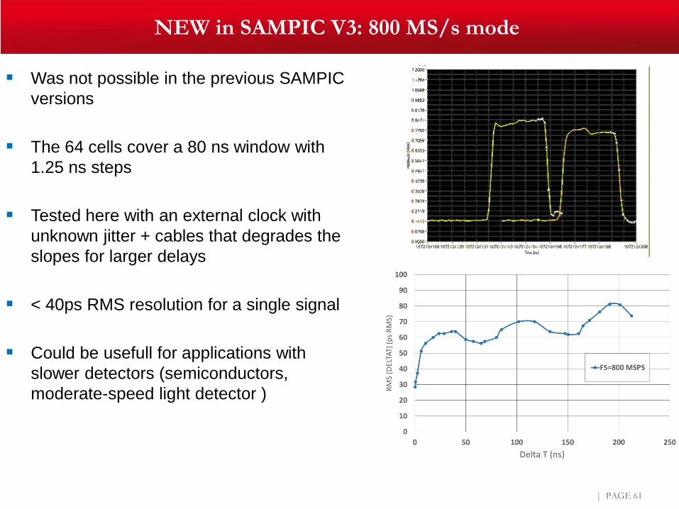
NEW in SAMPIC V3: 800 MS/s mode
Was not possible in the previous SAMPIC
versions
The 64 cells cover a 80 ns window with
1.25 ns steps
Tested here with an external clock with
unknown jitter + cables that degrades the
slopes for larger delays
< 40ps RMS resolution for a single signal
Could be usefull for applications with
slower detectors (semiconductors,
moderate-speed light detector )
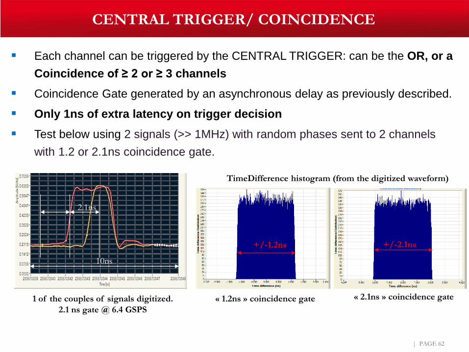
Each channel can be triggered by the CENTRAL TRIGGER: can be the OR, or a
Coincidence of ≥ 2 or ≥ 3 channels
Coincidence Gate generated by an asynchronous delay as previously described.
Only 1ns of extra latency on trigger decision
Test below using 2 signals (>> 1MHz) with random phases sent to 2 channels
with 1.2 or 2.1ns coincidence gate.
CENTRAL TRIGGER/ COINCIDENCE
| PAGE 62
10ns
2.1ns
TimeDifference histogram (from the digitized waveform)
1 of the couples of signals digitized.
2.1 ns gate @ 6.4 GSPS
« 1.2ns » coincidence gate « 2.1ns » coincidence gate
+/-2.1ns+/-1.2ns
SCAN TEST OF MCP-PMT
| PAGE 63
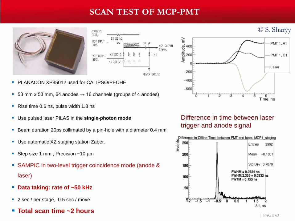
PLANACON XP85012 used for CALIPSO/PECHE
53 mm x 53 mm, 64 anodes → 16 channels (groups of 4 anodes)
Rise time 0.6 ns, pulse width 1.8 ns
Use pulsed laser PILAS in the single-photon mode
Beam duration 20ps collimated by a pin-hole with a diameter 0.4 mm
Use automatic XZ staging station Zaber.
Step size 1 mm , Precision ~10 µm
SAMPIC in two-level trigger coincidence mode (anode &
laser)
Data taking: rate of ~50 kHz
2 sec / per stage, 0.5 sec / move
Total scan time ~2 hours
Difference in time between laser
trigger and anode signal
© S. Sharyy
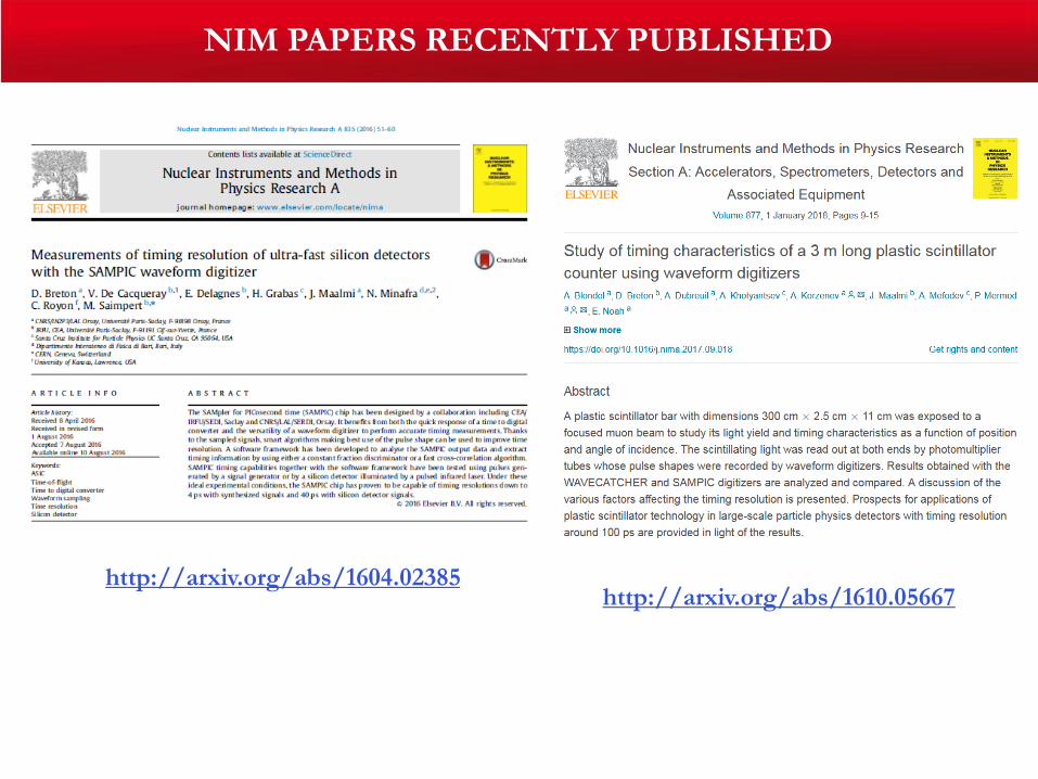
NIM PAPERS RECENTLY PUBLISHED
http://arxiv.org/abs/1604.02385http://arxiv.org/abs/1610.05667
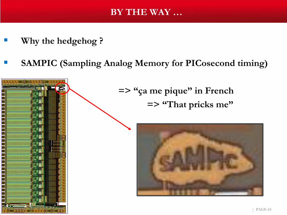
Why the hedgehog ?
SAMPIC (Sampling Analog Memory for PICosecond timing)
=> “ça me pique” in French
=> “That pricks me”
BY THE WAY …
| PAGE 65