Embed Size (px)
Citation preview
I. Introduction
During the last decades, MEMS technology hasundergone rapid development, leading to the suc-cessful fabrication of miniaturized mechanical
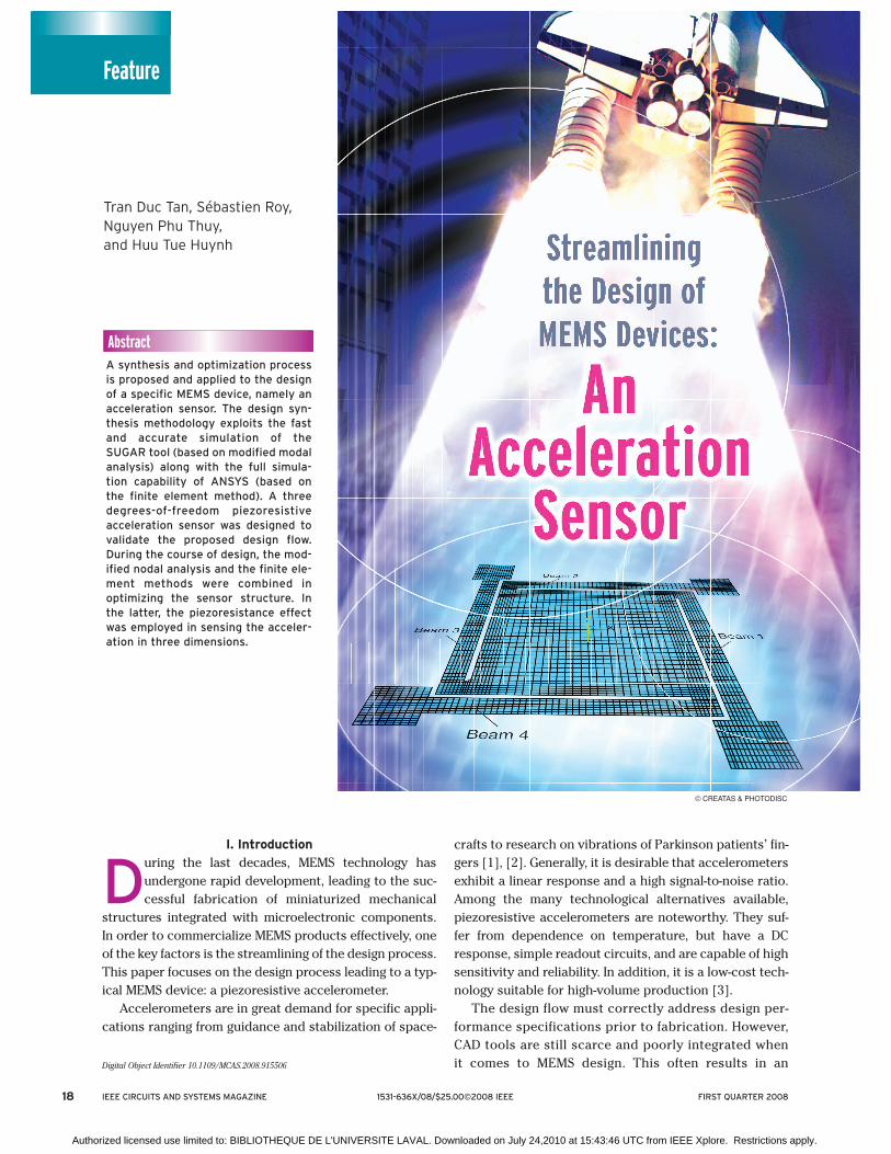
structures integrated with microelectronic components.In order to commercialize MEMS products effectively, oneof the key factors is the streamlining of the design process.This paper focuses on the design process leading to a typ-ical MEMS device: a piezoresistive accelerometer.
Accelerometers are in great demand for specific appli-cations ranging from guidance and stabilization of space-
crafts to research on vibrations of Parkinson patients’ fin-gers [1], [2]. Generally, it is desirable that accelerometersexhibit a linear response and a high signal-to-noise ratio.Among the many technological alternatives available,piezoresistive accelerometers are noteworthy. They suf-fer from dependence on temperature, but have a DCresponse, simple readout circuits, and are capable of highsensitivity and reliability. In addition, it is a low-cost tech-nology suitable for high-volume production [3].
The design flow must correctly address design per-formance specifications prior to fabrication. However,CAD tools are still scarce and poorly integrated whenit comes to MEMS design. This often results in an
18 IEEE CIRCUITS AND SYSTEMS MAGAZINE 1531-636X/08/$25.00©2008 IEEE FIRST QUARTER 2008
Tran Duc Tan, Sébastien Roy, Nguyen Phu Thuy,and Huu Tue Huynh
© CREATAS & PHOTODISC
Feature
A synthesis and optimization processis proposed and applied to the designof a specific MEMS device, namely anacceleration sensor. The design syn-thesis methodology exploits the fastand accurate simulation of theSUGAR tool (based on modified modalanalysis) along with the full simula-tion capability of ANSYS (based onthe finite element method). A threedegrees-of-freedom piezoresistiveacceleration sensor was designed tovalidate the proposed design flow.During the course of design, the mod-ified nodal analysis and the finite ele-ment methods were combined inoptimizing the sensor structure. Inthe latter, the piezoresistance effectwas employed in sensing the acceler-ation in three dimensions.
Abstract
Digital Object Identifier 10.1109/MCAS.2008.915506
Authorized licensed use limited to: BIBLIOTHEQUE DE L'UNIVERSITE LAVAL. Downloaded on July 24,2010 at 15:43:46 UTC from IEEE Xplore. Restrictions apply.
excessively lengthy design cycle [4], [5]. The SUGARwebsite [6], based at Berkeley, has this to say on theproblem: “In less than a decade, the MEMS communityhas leveraged nearly all the integrated-circuit commu-nity’s fabrication techniques, but little of the wealth ofsimulation capabilities. A wide range of student andprofessional circuit designers regularly use circuitsimulation tools like SPICE, while MEMS designersresort to back-of-the envelope calculations…”
One of the goals of this paper is to outline a fastdesign flow in order to reach multiple specified per-formance targets in a reasonable time frame. This isachieved by leveraging the best features of two radi-cally different simulation tools: Berkeley SUGAR, whichis an open-source academic effort, and ANSYS, which isa commercial product.
SUGAR espouses the philosophy of the venerable ICsimulation tool SPICE. It is based on modified nodalanalysis (MNA) and provides quick and accurate resultsat the system level [7], although it does employ someapproximations to make the device “fit” within its simu-lation mechanics.
We used SUGAR to sketch out quickly the structure ofthe accelerometer. It consists of a center mass connectedto four flexure beams comprised of a series of beams andanchors. Design goals for our configuration consist ofdesired resonant frequencies at the 1st, 2nd and 3rdmode. After iterating in SUGAR to converge towards thesegoals, an acceptable preliminary design was brought toANSYS for local optimization at the device level. Then, astress analysis was performed in order to determine thepositions of the doped piezoresistors on the four flexurebeams. The overall design and simulation effort using thistechnique is roughly 20 times shorter than with the built-in optimization function available within ANSYS.
II. Structure and Operation of
Piezoresistive Accelerometers
The three-degrees-of-freedom accelerometer alwaysrequires small cross-axial acceleration, high and linearsensitivity. We proposed a flexure configuration that is
19FIRST QUARTER 2008 IEEE CIRCUITS AND SYSTEMS MAGAZINE
Tran Duc Tan is with the College of Technology, Vietnam. E-mail: tantd@[email protected]. Sébastien Roy is with Laval University, Quebec, Canada. Email: [email protected]. Nguyen Phu Thuy is with the College of Technology and International Training Institute for Materials
Science, Vietnam. Email: [email protected]. H.T. Huynh is with BacHa International University, Vietnam. E-mail: [email protected].
Az
Ax, Ay
Figure 2. Cross-sectional view of motion along X, Y and Zaxes.
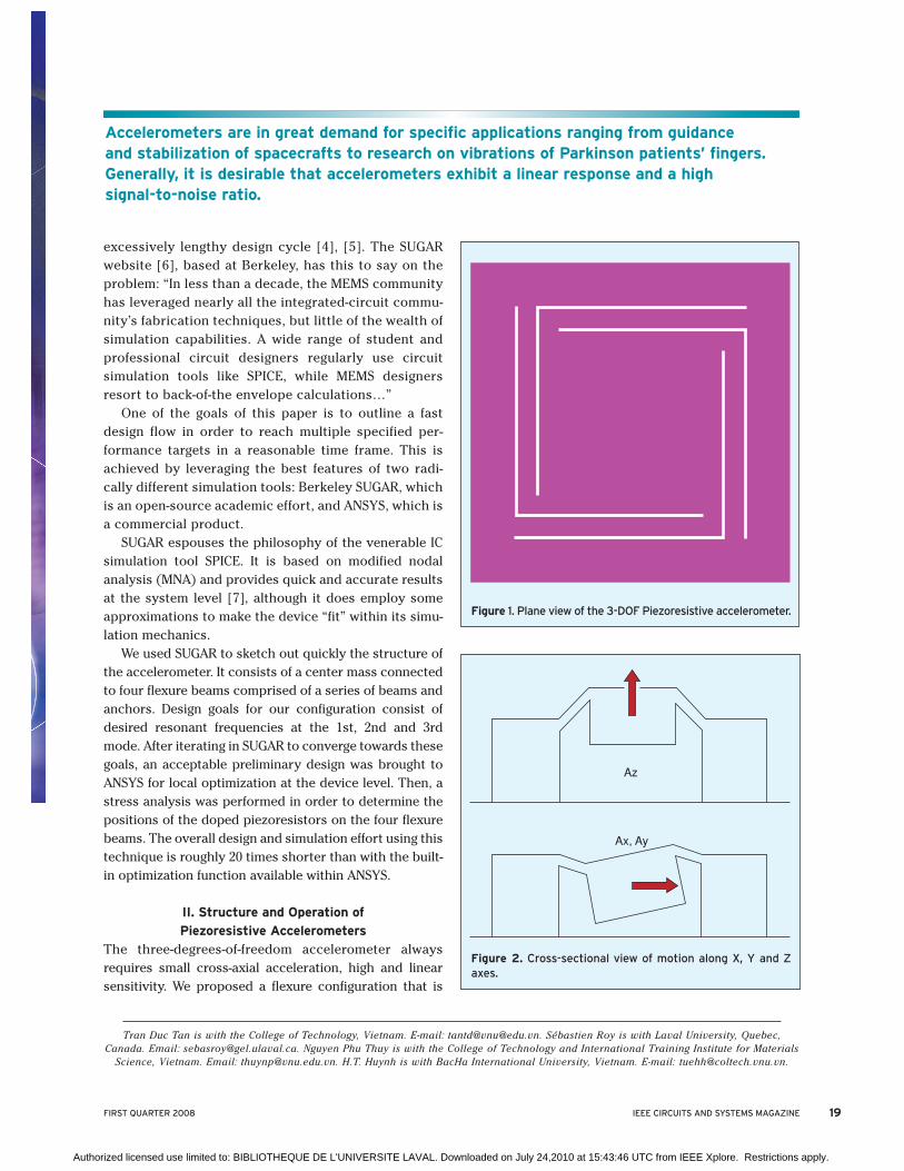
Figure 1. Plane view of the 3-DOF Piezoresistive accelerometer.
Accelerometers are in great demand for specific applications ranging from guidance and stabilization of spacecrafts to research on vibrations of Parkinson patients’ fingers.Generally, it is desirable that accelerometers exhibit a linear response and a highsignal-to-noise ratio.
Authorized licensed use limited to: BIBLIOTHEQUE DE L'UNIVERSITE LAVAL. Downloaded on July 24,2010 at 15:43:46 UTC from IEEE Xplore. Restrictions apply.
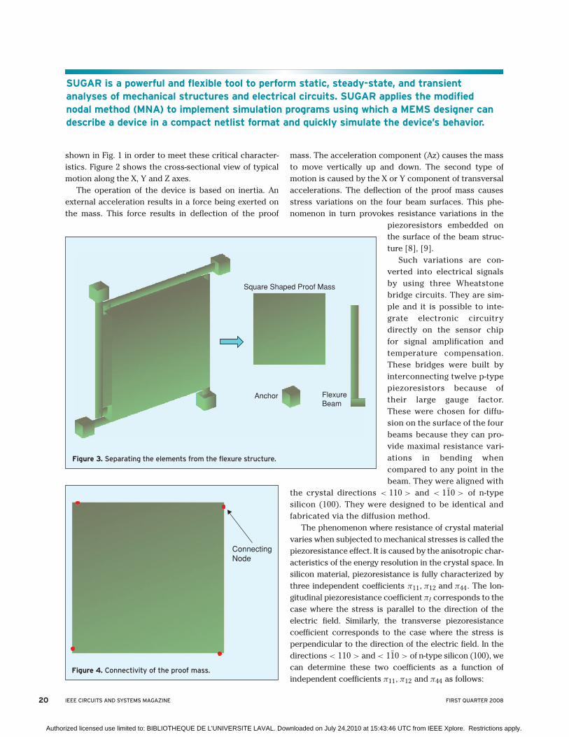
shown in Fig. 1 in order to meet these critical character-istics. Figure 2 shows the cross-sectional view of typicalmotion along the X, Y and Z axes.
The operation of the device is based on inertia. Anexternal acceleration results in a force being exerted onthe mass. This force results in deflection of the proof
mass. The acceleration component (Az) causes the massto move vertically up and down. The second type ofmotion is caused by the X or Y component of transversalaccelerations. The deflection of the proof mass causesstress variations on the four beam surfaces. This phe-nomenon in turn provokes resistance variations in the
piezoresistors embedded onthe surface of the beam struc-ture [8], [9].
Such variations are con-verted into electrical signalsby using three Wheatstonebridge circuits. They are sim-ple and it is possible to inte-grate electronic circuitrydirectly on the sensor chipfor signal amplification andtemperature compensation.These bridges were built byinterconnecting twelve p-typepiezoresistors because oftheir large gauge factor.These were chosen for diffu-sion on the surface of the fourbeams because they can pro-vide maximal resistance vari-ations in bending whencompared to any point in thebeam. They were aligned with
the crystal directions < 110 > and < 11̄0 > of n-typesilicon (100). They were designed to be identical andfabricated via the diffusion method.
The phenomenon where resistance of crystal materialvaries when subjected to mechanical stresses is called thepiezoresistance effect. It is caused by the anisotropic char-acteristics of the energy resolution in the crystal space. Insilicon material, piezoresistance is fully characterized bythree independent coefficients π11, π12 and π44. The lon-gitudinal piezoresistance coefficient πl corresponds to thecase where the stress is parallel to the direction of theelectric field. Similarly, the transverse piezoresistancecoefficient corresponds to the case where the stress isperpendicular to the direction of the electric field. In thedirections < 110 > and < 11̄0 > of n-type silicon (100), wecan determine these two coefficients as a function ofindependent coefficients π11, π12 and π44 as follows:
20
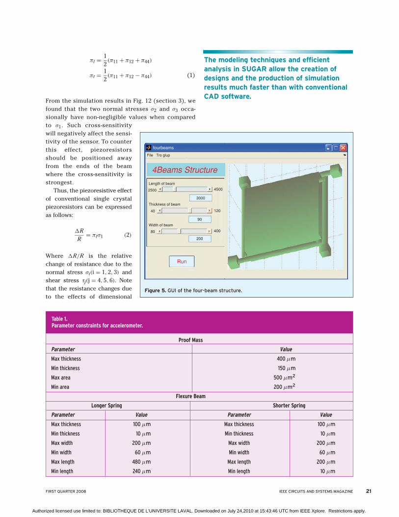
Square Shaped Proof Mass
Anchor FlexureBeam
Figure 3. Separating the elements from the flexure structure.
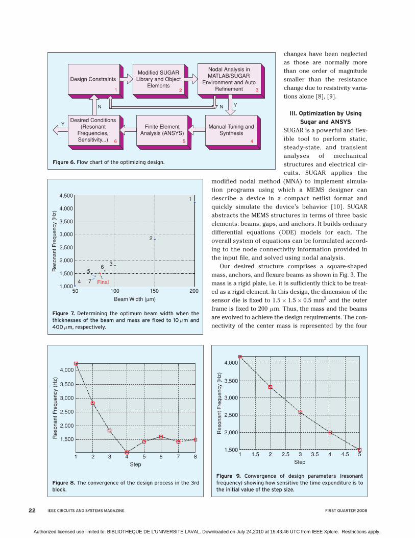
ConnectingNode
Figure 4. Connectivity of the proof mass.
SUGAR is a powerful and flexible tool to perform static, steady-state, and transientanalyses of mechanical structures and electrical circuits. SUGAR applies the modified nodal method (MNA) to implement simulation programs using which a MEMS designer candescribe a device in a compact netlist format and quickly simulate the device’s behavior.
IEEE CIRCUITS AND SYSTEMS MAGAZINE FIRST QUARTER 2008
Authorized licensed use limited to: BIBLIOTHEQUE DE L'UNIVERSITE LAVAL. Downloaded on July 24,2010 at 15:43:46 UTC from IEEE Xplore. Restrictions apply.
πl = 12(π11 + π12 + π44)
πt = 12(π11 + π12 − π44) (1)
From the simulation results in Fig. 12 (section 3), wefound that the two normal stresses σ2 and σ3 occa-sionally have non-negligible values when comparedto σ1 . Such cross-sensitivitywill negatively affect the sensi-tivity of the sensor. To counterthis effect, piezoresistorsshould be positioned awayfrom the ends of the beamwhere the cross-sensitivity isstrongest.
Thus, the piezoresistive effectof conventional single crystalpiezoresistors can be expressedas follows:
�RR
= πlσ1 (2)
Where �R/R is the relativechange of resistance due to thenormal stress σi(i = 1, 2, 3) andshear stress τj(j = 4, 5, 6). Notethat the resistance changes dueto the effects of dimensional
fourbeams
File Tro glup
4Beams StructureLength of beam
2500 4500
Thickness of beam
40
80
3000
120
200
Run
90
400
Width of beam
Figure 5. GUI of the four-beam structure.
Proof Mass
Parameter Value
Max thickness 400 μm
Min thickness 150 μm
Max area 500 μm2
Min area 200 μm2
Flexure Beam
Longer Spring Shorter Spring
Parameter Value Parameter Value
Max thickness 100 μm Max thickness 100 μm
Min thickness 10 μm Min thickness 10 μm
Max width 200 μm Max width 200 μm
Min width 60 μm Min width 60 μm
Max length 480 μm Max length 200 μm
Min length 240 μm Min length 10 μm
Table 1. Parameter constraints for accelerometer.
The modeling techniques and efficientanalysis in SUGAR allow the creation ofdesigns and the production of simulationresults much faster than with conventionalCAD software.
21FIRST QUARTER 2008 IEEE CIRCUITS AND SYSTEMS MAGAZINE
Authorized licensed use limited to: BIBLIOTHEQUE DE L'UNIVERSITE LAVAL. Downloaded on July 24,2010 at 15:43:46 UTC from IEEE Xplore. Restrictions apply.
changes have been neglectedas those are normally morethan one order of magnitudesmaller than the resistancechange due to resistivity varia-tions alone [8], [9].
III. Optimization by Using
Sugar and ANSYS
SUGAR is a powerful and flex-ible tool to perform static,steady-state, and transientanalyses of mechanicalstructures and electrical cir-cuits. SUGAR applies the
modified nodal method (MNA) to implement simula-tion programs using which a MEMS designer candescribe a device in a compact netlist format andquickly simulate the device’s behavior [10]. SUGARabstracts the MEMS structures in terms of three basicelements: beams, gaps, and anchors. It builds ordinarydifferential equations (ODE) models for each. Theoverall system of equations can be formulated accord-ing to the node connectivity information provided inthe input file, and solved using nodal analysis.
Our desired structure comprises a square-shapedmass, anchors, and flexure beams as shown in Fig. 3. Themass is a rigid plate, i.e. it is sufficiently thick to be treat-ed as a rigid element. In this design, the dimension of thesensor die is fixed to 1.5 × 1.5 × 0.5 mm3 and the outerframe is fixed to 200 μm. Thus, the mass and the beamsare evolved to achieve the design requirements. The con-nectivity of the center mass is represented by the four
22
4,5001
2
36
5
4 7 Final
4,000
3,500
3,000
2,500
2,000
1,500
1,00050 100
Beam Width (μm)
Res
onan
t Fre
quen
cy (
Hz)
150 200
Figure 7. Determining the optimum beam width when thethicknesses of the beam and mass are fixed to 10 μm and400 μm, respectively.
Desired Conditions(Resonant
Frequencies,Sensitivity...)
Design ConstraintsModified SUGAR
Library and ObjectElements
Nodal Analysis inMATLAB/SUGAR
Environment and AutoRefinement
Manual Tuning andSynthesis
Finite ElementAnalysis (ANSYS)
456
321
N N Y
Y
Figure 6. Flow chart of the optimizing design.
4,000
3,500
3,000
2,500
2,000
1,5001 1.5 2 2.5 3 3.5 4 4.5 5
Step
Res
onan
t Fre
quen
cy (
Hz)
Figure 9. Convergence of design parameters (resonantfrequency) showing how sensitive the time expenditure is tothe initial value of the step size.
4,000
3,500
3,000
2,500
2,000
1,500
1 2 3 4 5 6 7 8Step
Res
onan
t Fre
quen
cy (
Hz)
Figure 8. The convergence of the design process in the 3rdblock.
IEEE CIRCUITS AND SYSTEMS MAGAZINE FIRST QUARTER 2008
Authorized licensed use limited to: BIBLIOTHEQUE DE L'UNIVERSITE LAVAL. Downloaded on July 24,2010 at 15:43:46 UTC from IEEE Xplore. Restrictions apply.
nodes shown in Fig. 4. Positions of these connectingnodes are determined by parameters of the beams.
The MEMS designer can easily modify various processparameters such as Young’s modulus, Poisson’s ratio, theresidual stress, and the coefficient of thermal expansionin the process file [7].
The modeling techniques and efficient analysis inSUGAR allow the creation of designs and the productionof simulation results much faster than with conventionalCAD software [4]. Furthermore, its graphical user inter-face (GUI) provides convenient interactive visualizationcapabilities (see Fig. 5).
Two specification constraints are imposed on thestructure to be designed: (1) the natural frequency in theZ direction must be about 1500 Hz and (2) the natural fre-quency in the X (or Y) direction must be about 100 kHz.Furthermore, a set of parameter constraints is listed inTable 1. Note that the actions of various parameters areinterdependent.
A MEMS device can have a surface structure or a bulkstructure. Our case study accelerometer adopts the bulk-type structure. Figure 6 shows the mostly (90%) automat-ed synthesis flow that was used to evolve the final design.In the first three steps, an automatic refinement procedureis employed where the step size of a given parameter isvaried adaptively. For example, the step size of the beam’swidth (λ) is initially set at 50 μm. When the resonant fre-quency overshoots across the desired frequency, wemove back to the previous step point and scale back thestep size in order to reach the optimum point (see Fig. 7).
Figure 7 shows the resonantfrequency variation in terms ofthe beam width when we fixedthe beam thickness to a minimalvalue and the proof mass thick-ness to a maximal value in orderto get the maximum sensitivity.These extreme values are basedon process constraints, i.e.design rules. The beam widthwas iteratively refined in orderto make the first resonant fre-quency reach the desired value.We can see that the resonant fre-quency decreases rapidly whenthe beam width decreases. Ittakes 8 iterations to reach theoptimum value and the processovershoots twice.
Figure 8 shows again that thedesign process converges ineight steps. Theoretically, wecan get the exact desired
Size
Mass 845 × 845 × 400μm3
Beam 975 × 80 × 10μm3
Die Size 15 × 15 × 0.5μm3
Outer Frame Width 200μm
Table 2. Sensor parameters after manual tuning and synthesis block.
0 .380134.190067 .570202
.760269.950336
1.141.33
1.5211.711
MN
MX
X
Y
Z
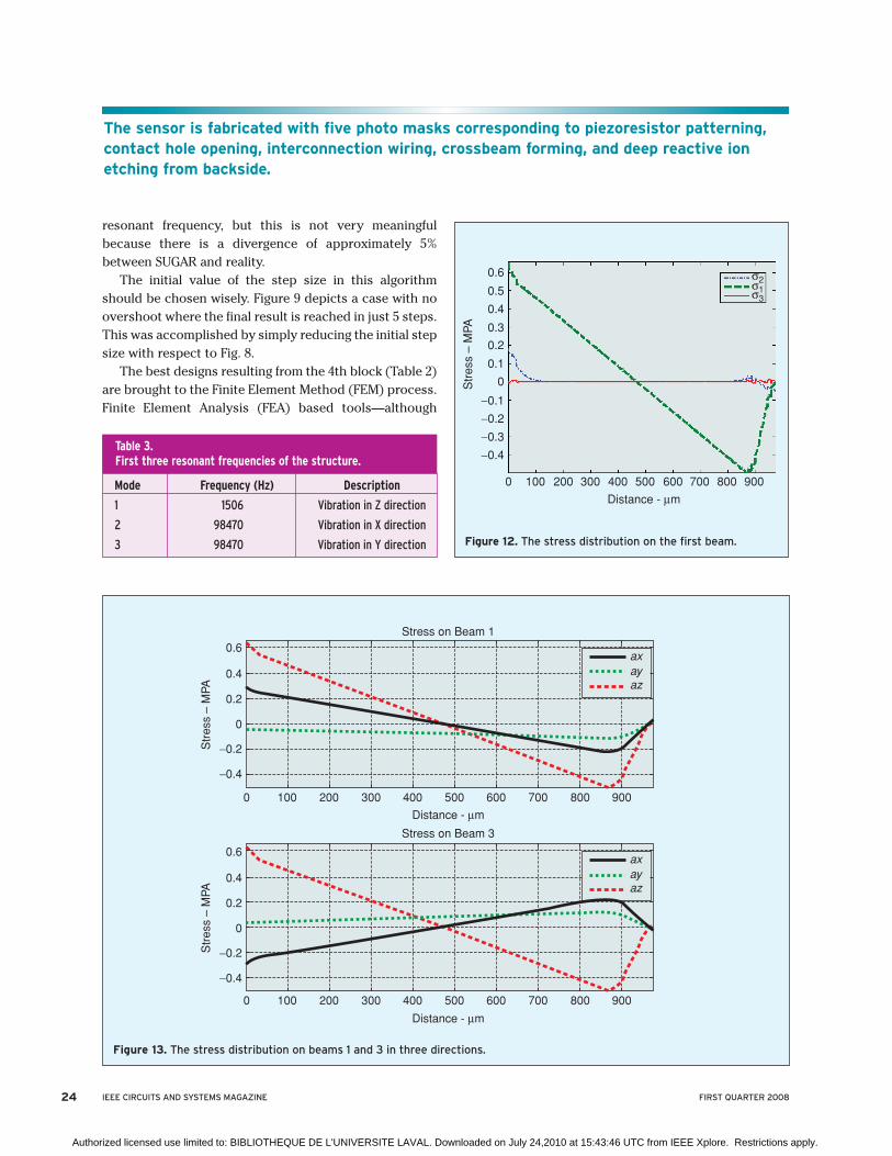
Figure 11. The stress distribution on the beams caused by the acceleration Az.
Beam 1
Y
XZ
Beam 2
Beam 3
Beam 4
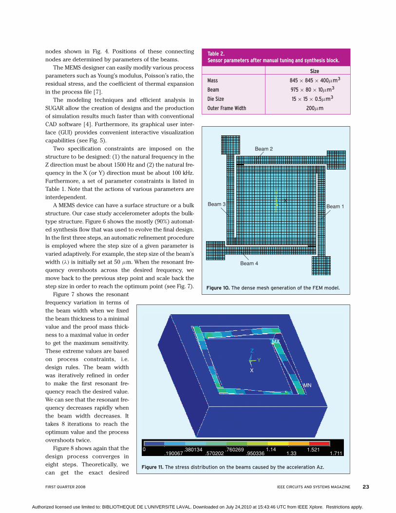
Figure 10. The dense mesh generation of the FEM model.
23FIRST QUARTER 2008 IEEE CIRCUITS AND SYSTEMS MAGAZINE
Authorized licensed use limited to: BIBLIOTHEQUE DE L'UNIVERSITE LAVAL. Downloaded on July 24,2010 at 15:43:46 UTC from IEEE Xplore. Restrictions apply.
resonant frequency, but this is not very meaningfulbecause there is a divergence of approximately 5%between SUGAR and reality.
The initial value of the step size in this algorithmshould be chosen wisely. Figure 9 depicts a case with noovershoot where the final result is reached in just 5 steps.This was accomplished by simply reducing the initial stepsize with respect to Fig. 8.
The best designs resulting from the 4th block (Table 2)are brought to the Finite Element Method (FEM) process.Finite Element Analysis (FEA) based tools—although
Mode Frequency (Hz) Description
1 1506 Vibration in Z direction
2 98470 Vibration in X direction
3 98470 Vibration in Y direction
Table 3. First three resonant frequencies of the structure.
Stress on Beam 1
Distance - μm
0
0.6
0.4
0.2
0
−0.2
−0.4
0.6
0.4
0.2
0
−0.2
−0.4
100 200 300 400 500 600 700 800 900
0 100 200 300 400 500 600 700 800 900
Distance - μm
Stress on Beam 3
Str
ess
– M
PAS
tres
s –
MPA
axayaz
axayaz
Figure 13. The stress distribution on beams 1 and 3 in three directions.
0.6
0.5
0.4
0.3
0.2
0.1
Str
ess
– M
PA
0
−0.1
−0.2
−0.3
−0.4
0 100 200 300 400 500
Distance - μm
600 700 800 900
σ2σ1σ3
Figure 12. The stress distribution on the first beam.
The sensor is fabricated with five photo masks corresponding to piezoresistor patterning,contact hole opening, interconnection wiring, crossbeam forming, and deep reactive ionetching from backside.
24 IEEE CIRCUITS AND SYSTEMS MAGAZINE FIRST QUARTER 2008
Authorized licensed use limited to: BIBLIOTHEQUE DE L'UNIVERSITE LAVAL. Downloaded on July 24,2010 at 15:43:46 UTC from IEEE Xplore. Restrictions apply.
complex—yield more complete and precise numericalresults and especially are more flexible in choosing thedevice geometry.
SUGAR is a simplified simulation method and istherefore prone to imprecisions of various kinds. Themain source of error in our case stems from beam over-lap. In exchange for much faster simulation speed,SUGAR does not include the actual conditions at theend of the beam. Instead, SUGAR assumes a fixed con-nection exactly at the node point. In fact, when twobeams connect at an angle, especially an acute angle,there is some physical overlap in their areas (see Fig.3—flexure beam) within the SUGAR model. This prob-lem can be avoided in ANSYS by joining all the beampolygons into a single polygon through a union opera-tion, such that overlapping areas are subsumed.
Above all other considerations, the most importantaspect of FEA in our design process is the analysis of thestress distribution in the flexure beams. Based on this dis-tribution, piezoresistors are positioned to eliminatecross-axis sensitivities and to maximize the sensitivity tothe three acceleration components.
Now, we will consider the stress states on the surface ofthe beams due to each individual component of force andmoment applied separately. Note that all calculations arebased on the isotropic material assumption. Figure 10shows the mesh generation for analysis and the stress dis-tribution on the beam is shown in Fig. 11. There are sever-al solvers available in ANSYS for modal analysis and theBlock-Lanczos solver was used for this case. The frequen-cies from the first to third mode obtained by FEM are list-ed in Table 3.
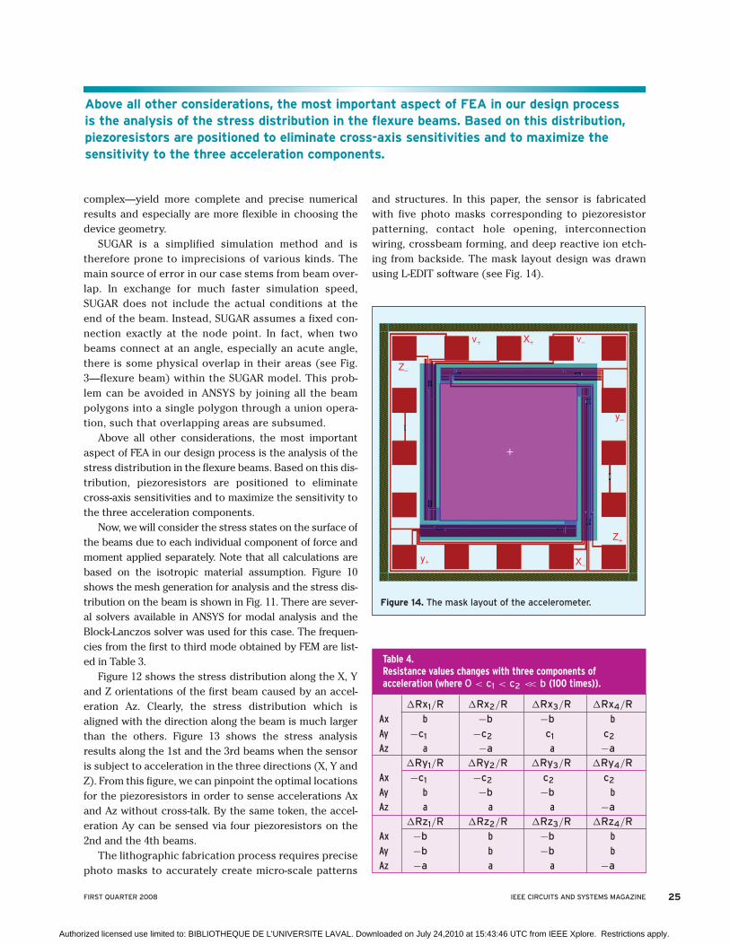
Figure 12 shows the stress distribution along the X, Yand Z orientations of the first beam caused by an accel-eration Az. Clearly, the stress distribution which isaligned with the direction along the beam is much largerthan the others. Figure 13 shows the stress analysisresults along the 1st and the 3rd beams when the sensoris subject to acceleration in the three directions (X, Y andZ). From this figure, we can pinpoint the optimal locationsfor the piezoresistors in order to sense accelerations Axand Az without cross-talk. By the same token, the accel-eration Ay can be sensed via four piezoresistors on the2nd and the 4th beams.
The lithographic fabrication process requires precisephoto masks to accurately create micro-scale patterns
and structures. In this paper, the sensor is fabricatedwith five photo masks corresponding to piezoresistorpatterning, contact hole opening, interconnectionwiring, crossbeam forming, and deep reactive ion etch-ing from backside. The mask layout design was drawnusing L-EDIT software (see Fig. 14).
v+ X+ v−
y−
y+
Z+
Z−
+
X−
Figure 14. The mask layout of the accelerometer.
�Rx1/R �Rx2/R �Rx3/R �Rx4/RAx b −b −b bAy −c1 −c2 c1 c2
Az a −a a −a�Ry1/R �Ry2/R �Ry3/R �Ry4/R
Ax −c1 −c2 c2 c2
Ay b −b −b bAz a a a −a
�Rz1/R �Rz2/R �Rz3/R �Rz4/RAx −b b −b bAy −b b −b bAz −a a a −a
Table 4. Resistance values changes with three components ofacceleration (where 0 < c1 < c2 << b (100 times)).
25FIRST QUARTER 2008 IEEE CIRCUITS AND SYSTEMS MAGAZINE
Above all other considerations, the most important aspect of FEA in our design process is the analysis of the stress distribution in the flexure beams. Based on this distribution,piezoresistors are positioned to eliminate cross-axis sensitivities and to maximize thesensitivity to the three acceleration components.
Authorized licensed use limited to: BIBLIOTHEQUE DE L'UNIVERSITE LAVAL. Downloaded on July 24,2010 at 15:43:46 UTC from IEEE Xplore. Restrictions apply.
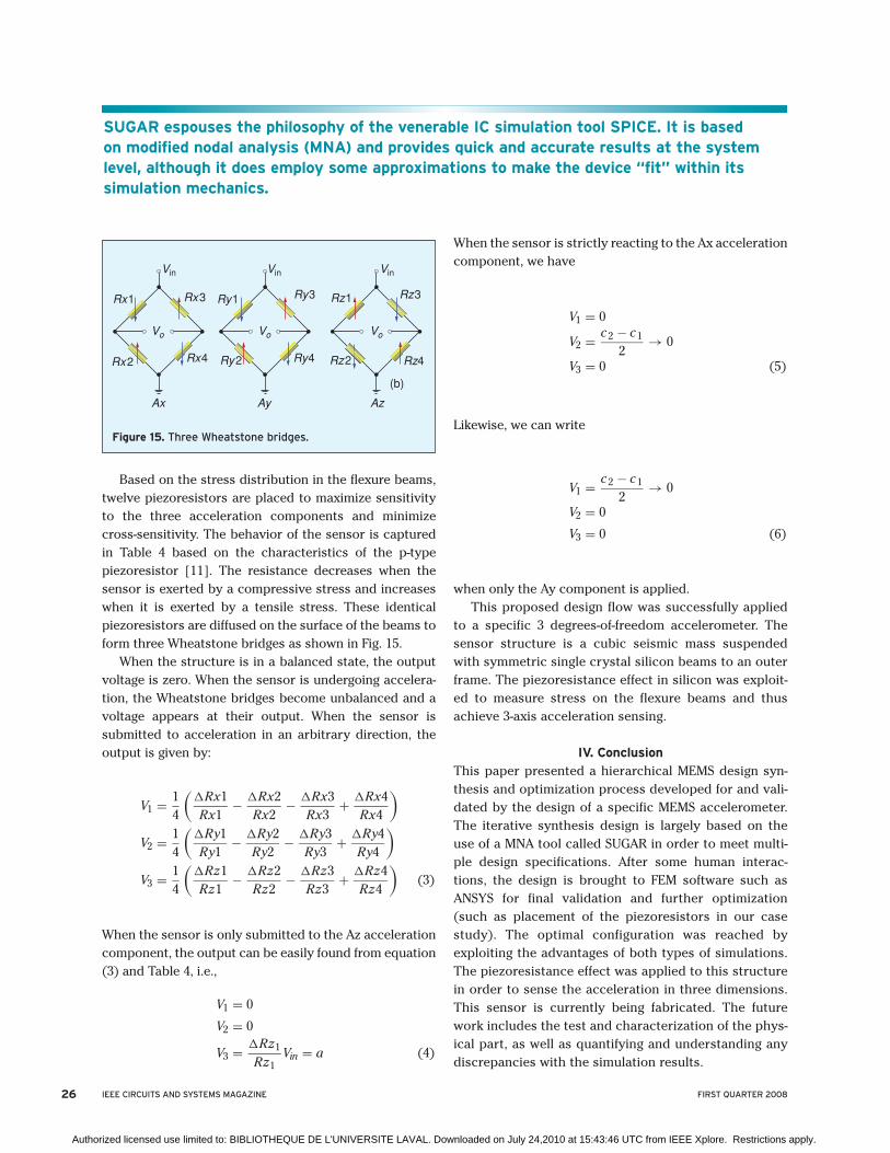
Based on the stress distribution in the flexure beams,twelve piezoresistors are placed to maximize sensitivityto the three acceleration components and minimizecross-sensitivity. The behavior of the sensor is capturedin Table 4 based on the characteristics of the p-typepiezoresistor [11]. The resistance decreases when thesensor is exerted by a compressive stress and increaseswhen it is exerted by a tensile stress. These identicalpiezoresistors are diffused on the surface of the beams toform three Wheatstone bridges as shown in Fig. 15.
When the structure is in a balanced state, the outputvoltage is zero. When the sensor is undergoing accelera-tion, the Wheatstone bridges become unbalanced and avoltage appears at their output. When the sensor issubmitted to acceleration in an arbitrary direction, theoutput is given by:
V1 = 14
(�Rx1Rx1
− �Rx2Rx2
− �Rx3Rx3
+ �Rx4Rx4
)
V2 = 14
(�Ry1Ry1
− �Ry2Ry2
− �Ry3Ry3
+ �Ry4Ry4
)
V3 = 14
(�Rz1Rz1
− �Rz2Rz2
− �Rz3Rz3
+ �Rz4Rz4
)(3)
When the sensor is only submitted to the Az accelerationcomponent, the output can be easily found from equation(3) and Table 4, i.e.,
V1 = 0
V2 = 0
V3 = �Rz1
Rz1Vin = a (4)
When the sensor is strictly reacting to the Ax accelerationcomponent, we have
V1 = 0
V2 = c2 − c1
2→ 0
V3 = 0 (5)
Likewise, we can write
V1 = c2 − c1
2→ 0
V2 = 0
V3 = 0 (6)
when only the Ay component is applied.This proposed design flow was successfully applied
to a specific 3 degrees-of-freedom accelerometer. Thesensor structure is a cubic seismic mass suspendedwith symmetric single crystal silicon beams to an outerframe. The piezoresistance effect in silicon was exploit-ed to measure stress on the flexure beams and thusachieve 3-axis acceleration sensing.
IV. Conclusion
This paper presented a hierarchical MEMS design syn-thesis and optimization process developed for and vali-dated by the design of a specific MEMS accelerometer.The iterative synthesis design is largely based on theuse of a MNA tool called SUGAR in order to meet multi-ple design specifications. After some human interac-tions, the design is brought to FEM software such asANSYS for final validation and further optimization(such as placement of the piezoresistors in our casestudy). The optimal configuration was reached byexploiting the advantages of both types of simulations.The piezoresistance effect was applied to this structurein order to sense the acceleration in three dimensions.This sensor is currently being fabricated. The futurework includes the test and characterization of the phys-ical part, as well as quantifying and understanding anydiscrepancies with the simulation results.
26
SUGAR espouses the philosophy of the venerable IC simulation tool SPICE. It is based on modified nodal analysis (MNA) and provides quick and accurate results at the systemlevel, although it does employ some approximations to make the device “fit” within itssimulation mechanics.
Rx1
Vin
Vo Vo Vo
Vin Vin
Rx2 Rx4
Rx3 Ry1
Ry2 Ry4
Ry3 Rz1
Rz2 Rz4
Rz3
Ax Ay Az
(b)
Figure 15. Three Wheatstone bridges.
IEEE CIRCUITS AND SYSTEMS MAGAZINE FIRST QUARTER 2008
Authorized licensed use limited to: BIBLIOTHEQUE DE L'UNIVERSITE LAVAL. Downloaded on July 24,2010 at 15:43:46 UTC from IEEE Xplore. Restrictions apply.
References[1] L.C. Spangler and C.J. Kemp, “Integrated silicon automotiveaccelerometer,” Sens. Actuators, A54, pp. 523–529, 1996.[2] T. Velten, P. Krause, and E. Obermeier, “Two-axis MicromachinedAccelerometer for Gesture Recognition,” MME, 1996, pp. 247–250.[3] A. Garcia-Valenzuela and M. Tabib-Azar, “Comparative study of piezo-electric, piezoresistive, electrostatic, magnetic, and optical sensors,”Proc. SPIE, 1994, pp. 125–142.[4] J.V. Clark, D. Bindel, N. Zhou, J. Nie, W. Kao, E. Zhu, A. Kuo, K.S.J.Pister, J. Demmel, S. Govindjee, Z. Bai, M. Gu, and A.M. Agogino,“Addressing the Needs of Complex MEMS Design,” in Proceedings of the15th IEEE International MEMS Conference, 2002, pp. 204–209.[5] N. Zhou, B. Zhu, A.M. Agogino, and K.S.J. Pister, “Evolutionary Syn-thesis of MEMS (Microelectronic Mechanical Systems) Design,” in Pro-ceedings of ANNIE, Intelligent Engineering Systems through Artificial NeuralNetworks, ASME Press, vol. 11, pp. 197–202, 2001.[6] http://www-bsac.eecs.berkeley.edu/cadtools/sugar/sugar/[7] J.V. Clark, N. Zhou, D. Bindel, L. Schenato, W. Wu, J. Demmel, and K.S.J.Pister, “3D MEMS Simulation Modeling Using Modified Nodal Analysis,”Tech. Digest, Solid-State Sensor and Actuator Workshop, pp. 191–196, 2002.[8] Y. Kanda, “Graphical representation of the piezoresistance coeffi-cients in Si shear coefficients in plane,” Japanese J. Appl. Phys., vol. 26,no. 7, pp. 1031–1033, 1987.[9] D.V. Dao, T. Toriyama, J. Wells, and S. Sugiyama, “Silicon Piezoresis-tive Six-Degree of Freedom Force-Moment Micro Sensor,” Sensors andMaterials, vol. 15, no. 3, pp. 113–135, 2003.[10] J.V. Clark, D. Bindel, N. Zhou, S. Bhave, Z. Bai, J. Demmel, and K.S.J.Pister, “Advancements in 3D Multi Domain Simulation Package forMEMS,” Proceeding of the Micro scales Systems, pp. 40–45, 2001.[11] T. Toriyama and S. Sugiyama, “Analysis of piezoresistance in p-typesilicon for mechanical sensors,” IEEE J. MEMS 11 598, pp. 598–604, 2002.
Tran Duc Tan was born in 1980. Hereceived the B.Sc. and M.Sc. degrees,respectively, in 2002 and in 2005, from theCollege of Technology (COLTECH), Viet-nam National University—Hanoi, Vietnam(VNU), where he has been a lecturer since2006. He is currently completing the Ph.D.
thesis at COLTECH, VNUH. He is author and coauthor ofseveral papers on capacitive accelerometers, siliconmicromachined gyroscopes, and piezoresistive accelerom-eters. His present research interest is in the developmentof MEMS-based inertial navigation systems.
Sébastien Roy (S’95-M’02) received theB.Sc. and M.Sc. degrees in electricalengineering from Laval University,Québec, QC, Canada, in 1991 and 1993,respectively, and the Ph.D. degree fromCarleton University, Ottawa, ON, Cana-da, in 2000. He is currently an Associate
Professor with the Department of Electrical and Com-puter Engineering, Laval University, where he is pursu-ing research in the system-level and implementationaspects of signal processing for communications as wellas space-time processing and space-time coding. From2000 to 2002, he was a Natural Sciences and EngineeringResearch Council of Canada (NSERC) Postdoctoral Fel-low at Laval University. He has also been active in indus-trial consulting and was involved in the organization of
several international conference. In 2007, he was aninvited professor at l’École Nationale Supérieure de Sci-ences Appliquées et de Technologie (ENSSAT), Lannion,France. He received multiple teaching awards and in2007 received the award for excellence in technologytransfer from the strategic network on Systems andTechnologies for Advanced Communications (SYTA-com). Dr. Roy was also awarded the award for Post-Grad-uate Research Excellence from the Canadian Institutefor Telecommunications Research in 2000.
Nguyen Phu Thuy received the Ph.D.degree in 1979 at Charles University,Prague, Czechoslovakia. Since 1980, hehas been a faculty member of the VietnamNational University, Hanoi (VNUH). He hasalso been associated to InternationalTraining Institute for Materials Science
(ITIMS) since 1992 as senior researcher. In 2005, he wasnominated Dean of the Faculty of Electronics and Telecom-munications, College of Technology, VNUH. He is authorand coauthor of more than one hundred papers publishedin professional journals and international conferences. Hisresearch interests cover magnetic materials and MEMS-based sensors with applications.
Huu Tue Huynh received the Sc.D. fromLaval University in 1972, where he hadbeen a Professor of the Department Elec-trical and Computer Engineering since1969. He left Laval in 2004 to become theChairman of the Department of Informa-tion Processing of the College of Tech-
nology, Vietnam National University, Hanoi and recentlynominated Rector of Bac Ha International University. Hehas been an invited professor at l’INSA (Lyon, France) in1972, ENST (Paris, France) in 1980, l’Universite deRennes (France) in 1982, Concordia University (Montre-al, Canada) in 1985, Ecole Polytechnique (Montreal,Canada) in 1986, l’Universite de Sherbrooke (Sher-brooke, Canada), in 1990, CEPHAG (Grenoble, France) in1995. In 1984, he was an invited guest of Bell Lab (Nep-tune, N.J. USA). He is author and coauthor of more thanone hundred papers published in professional journalsand international conferences; he is also coauthor of twobooks, “Systemes non-lineaires” (Gordon & Breach 1972)and “Simulations stochastiques et applications enFinances avec des Programmes Matlab” (Economica,2006); the English version of the second book will bepublished by Wiley in 2008. His research interests coverstochastic simulation techniques, information process-ing, fast algorithms and architectures with applicationsto digital communications.
27FIRST QUARTER 2008 IEEE CIRCUITS AND SYSTEMS MAGAZINE
Authorized licensed use limited to: BIBLIOTHEQUE DE L'UNIVERSITE LAVAL. Downloaded on July 24,2010 at 15:43:46 UTC from IEEE Xplore. Restrictions apply.