Embed Size (px)
Citation preview
Datasheet
3A 150KHZ PWM Buck DC/DC Converter TD1501
October, 20, 2005 Techcode Semiconductor Limited
1
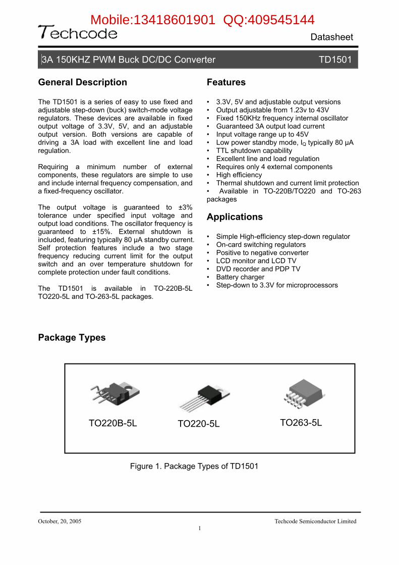
General Description The TD1501 is a series of easy to use fixed and adjustable step-down (buck) switch-mode voltage regulators. These devices are available in fixed output voltage of 3.3V, 5V, and an adjustable output version. Both versions are capable of driving a 3A load with excellent line and load regulation. Requiring a minimum number of external components, these regulators are simple to use and include internal frequency compensation, and a fixed-frequency oscillator. The output voltage is guaranteed to ±3% tolerance under specified input voltage and output load conditions. The oscillator frequency is guaranteed to ±15%. External shutdown is included, featuring typically 80 µA standby current. Self protection features include a two stage frequency reducing current limit for the output switch and an over temperature shutdown for complete protection under fault conditions. The TD1501 is available in TO-220B-5L TO220-5L and TO-263-5L packages.
Features • 3.3V, 5V and adjustable output versions • Output adjustable from 1.23v to 43V • Fixed 150KHz frequency internal oscillator • Guaranteed 3A output load current • Input voltage range up to 45V • Low power standby mode, IQ typically 80 µA • TTL shutdown capability • Excellent line and load regulation • Requires only 4 external components • High efficiency • Thermal shutdown and current limit protection • Available in TO-220B/TO220 and TO-263 packages Applications • Simple High-efficiency step-down regulator • On-card switching regulators • Positive to negative converter • LCD monitor and LCD TV • DVD recorder and PDP TV • Battery charger • Step-down to 3.3V for microprocessors
Package Types
TO220B-5L TO263-5L
Figure 1. Package Types of TD1501
TO220-5L
Mobile:13418601901 QQ:409545144
Datasheet
3A 150KHZ PWM Buck DC/DC Converter TD1501
October, 20, 2005 Techcode Semiconductor Limited
2
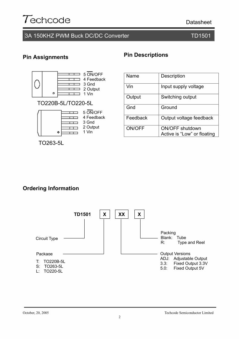
Pin Assignments
Pin Descriptions
Ordering Information
Name Description
Vin Input supply voltage
Output Switching output
Gnd Ground
Feedback Output voltage feedback
ON/OFF ON/OFF shutdown Active is “Low” or floating
5 ON/OFF 4 Feedback 3 Gnd 2 Output 1 Vin
5 ON/OFF 4 Feedback3 Gnd 2 Output 1 Vin
TO220B-5L/TO220-5L
TO263-5L
X XX XTD1501
Circuit Type
Package
T: TO220B-5L S: TO263-5L L: TO220-5L
Output Versions ADJ: Adjustable Output 3.3: Fixed Output 3.3V 5.0: Fixed Output 5V
Packing Blank: Tube R: Type and Reel
Datasheet
3A 150KHZ PWM Buck DC/DC Converter TD1501
October, 20, 2005 Techcode Semiconductor Limited
3
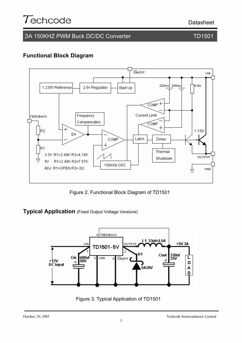
Functional Block Diagram
Typical Application (Fixed Output Voltage Versions)
Figure 2. Functional Block Diagram of TD1501
Figure 3. Typical Application of TD1501
Datasheet
3A 150KHZ PWM Buck DC/DC Converter TD1501
October, 20, 2005 Techcode Semiconductor Limited
4
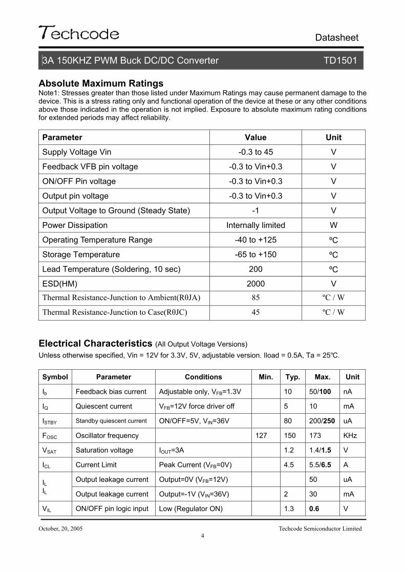
Absolute Maximum Ratings Note1: Stresses greater than those listed under Maximum Ratings may cause permanent damage to the device. This is a stress rating only and functional operation of the device at these or any other conditions above those indicated in the operation is not implied. Exposure to absolute maximum rating conditions for extended periods may affect reliability.
Parameter Value Unit
Supply Voltage Vin -0.3 to 45 V
Feedback VFB pin voltage -0.3 to Vin+0.3 V
ON/OFF Pin voltage -0.3 to Vin+0.3 V
Output pin voltage -0.3 to Vin+0.3 V
Output Voltage to Ground (Steady State) -1 V
Power Dissipation Internally limited W
Operating Temperature Range -40 to +125 ºC
Storage Temperature -65 to +150 ºC
Lead Temperature (Soldering, 10 sec) 200 ºC
ESD(HM) 2000 V Thermal Resistance-Junction to Ambient(RθJA) 85 ºC / W
Thermal Resistance-Junction to Case(RθJC) 45 ºC / W Electrical Characteristics (All Output Voltage Versions) Unless otherwise specified, Vin = 12V for 3.3V, 5V, adjustable version. Iload = 0.5A, Ta = 25. Symbol Parameter Conditions Min. Typ. Max. Unit
Ib Feedback bias current Adjustable only, VFB=1.3V 10 50/100 nA
IQ Quiescent current VFB=12V force driver off 5 10 mA
ISTBY Standby quiescent current ON/OFF=5V, VIN=36V 80 200/250 uA
FOSC Oscillator frequency 127 150 173 KHz
VSAT Saturation voltage IOUT=3A 1.2 1.4/1.5 V
ICL Current Limit Peak Current (VFB=0V) 4.5 5.5/6.5 A
Output leakage current Output=0V (VFB=12V) 50 uA IL IL Output leakage current Output=-1V (VIN=36V) 2 30 mA
VIL ON/OFF pin logic input Low (Regulator ON) 1.3 0.6 V
Datasheet
3A 150KHZ PWM Buck DC/DC Converter TD1501
October, 20, 2005 Techcode Semiconductor Limited
5
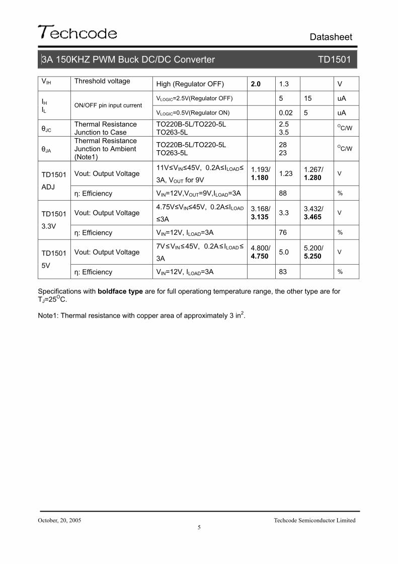
VIH Threshold voltage High (Regulator OFF) 2.0 1.3 V
VLOGIC=2.5V(Regulator OFF) 5 15 uA IH IL
ON/OFF pin input current VLOGIC=0.5V(Regulator ON) 0.02 5 uA
θJC Thermal Resistance Junction to Case
TO220B-5L/TO220-5L TO263-5L 2.5
3.5 OC/W
θJA Thermal Resistance Junction to Ambient (Note1)
TO220B-5L/TO220-5L TO263-5L 28
23 OC/W
Vout: Output Voltage 11V≤VIN≤45V, 0.2A≤ILOAD≤3A, VOUT for 9V
1.193/1.180 1.23 1.267/
1.280 V TD1501 ADJ
η: Efficiency VIN=12V,VOUT=9V,ILOAD=3A 88 %
Vout: Output Voltage 4.75V≤VIN≤45V, 0.2A≤ILOAD
≤3A 3.168/3.135 3.3 3.432/
3.465 V TD1501 3.3V
η: Efficiency VIN=12V, ILOAD=3A 76 %
Vout: Output Voltage 7V≤VIN≤45V, 0.2A≤ILOAD≤3A
4.800/4.750 5.0 5.200/
5.250 V TD1501 5V
η: Efficiency VIN=12V, ILOAD=3A 83 %
Specifications with boldface type are for full operationg temperature range, the other type are for TJ=25OC. Note1: Thermal resistance with copper area of approximately 3 in2.
Datasheet
3A 150KHZ PWM Buck DC/DC Converter TD1501
October, 20, 2005 Techcode Semiconductor Limited
6
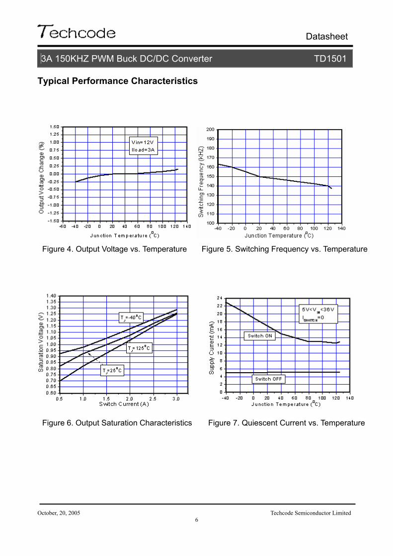
Typical Performance Characteristics
Figure 4. Output Voltage vs. Temperature Figure 5. Switching Frequency vs. Temperature
Figure 6. Output Saturation Characteristics Figure 7. Quiescent Current vs. Temperature
Datasheet
3A 150KHZ PWM Buck DC/DC Converter TD1501
October, 20, 2005 Techcode Semiconductor Limited
7
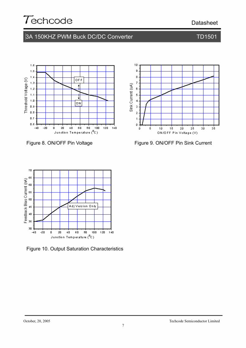
Figure 8. ON/OFF Pin Voltage Figure 9. ON/OFF Pin Sink Current
Figure 10. Output Saturation Characteristics
Datasheet
3A 150KHZ PWM Buck DC/DC Converter TD1501
October, 20, 2005 Techcode Semiconductor Limited
8
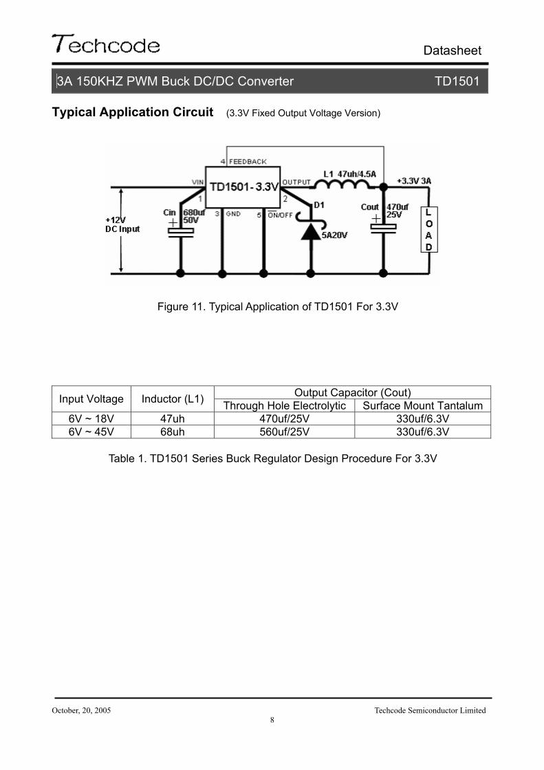
Typical Application Circuit (3.3V Fixed Output Voltage Version)
Output Capacitor (Cout) Input Voltage Inductor (L1) Through Hole Electrolytic Surface Mount Tantalum6V ~ 18V 47uh 470uf/25V 330uf/6.3V 6V ~ 45V 68uh 560uf/25V 330uf/6.3V
Figure 11. Typical Application of TD1501 For 3.3V
Table 1. TD1501 Series Buck Regulator Design Procedure For 3.3V
Datasheet
3A 150KHZ PWM Buck DC/DC Converter TD1501
October, 20, 2005 Techcode Semiconductor Limited
9
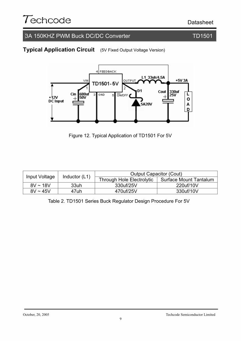
Typical Application Circuit (5V Fixed Output Voltage Version)
Output Capacitor (Cout) Input Voltage Inductor (L1) Through Hole Electrolytic Surface Mount Tantalum8V ~ 18V 33uh 330uf/25V 220uf/10V 8V ~ 45V 47uh 470uf/25V 330uf/10V
Figure 12. Typical Application of TD1501 For 5V
Table 2. TD1501 Series Buck Regulator Design Procedure For 5V
Datasheet
3A 150KHZ PWM Buck DC/DC Converter TD1501
October, 20, 2005 Techcode Semiconductor Limited
10
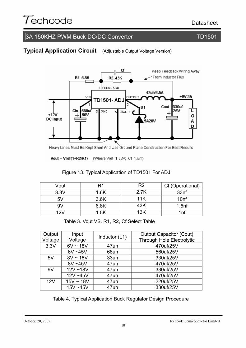
Typical Application Circuit (Adjustable Output Voltage Version)
Vout R1 R2 Cf (Operational) 3.3V 1.6K 2.7K 33nf 5V 3.6K 11K 10nf 9V 6.8K 43K 1.5nf
12V 1.5K 13K 1nf
Output Capacitor (Cout) Output Voltage
Input Voltage Inductor (L1) Through Hole Electrolytic
6V ~ 18V 47uh 470uf/25V 3.3V 6V ~45V 68uh 560uf/25V 8V ~ 18V 33uh 330uf/25V 5V 8V ~45V 47uh 470uf/25V
12V ~18V 47uh 330uf/25V 9V 12V ~45V 47uh 470uf/25V 15V ~ 18V 47uh 220uf/25V 12V 15V ~45V 47uh 330uf/25V
Figure 13. Typical Application of TD1501 For ADJ
Table 3. Vout VS. R1, R2, Cf Select Table
Table 4. Typical Application Buck Regulator Design Procedure
Datasheet
3A 150KHZ PWM Buck DC/DC Converter TD1501
October, 20, 2005 Techcode Semiconductor Limited
11
Function Description Pin Functions +VIN This is the positive input supply for the IC switching regulator. A suitable input bypass capacitor must be present at this pin to minimize voltage transients and to supply the switching currents needed by the regulator Ground Circuit ground. Output Internal switch. The voltage at this pin switches between (+VIN – VSAT) and approximately – 0.5V, with a duty cycle of approximately VOUT / VIN. To minimize coupling to sensitive circuitry, the PC board copper area connected to this pin should be kept a minimum. Feedback Senses the regulated output voltage to complete the feedback loop. ON/OFF Allows the switching regulator circuit to be shutdown using logic level signals thus dropping the total input supply current to approximately 80uA. Pulling this pin below a threshold voltage of approximately 1.3V turns the regulator on, and pulling this pin above 1.3V (up to a maximum of 25V) shuts the regulator down. If this shutdown feature is not needed, the ON /OFF pin can be wired to the ground pin or it can be left open, in either case the regulator will be in the ON condition. Thermal Considerations The TD1501 is available in two packages, a 5-pin TO-220B/TO-220 and a 5-pin surface mount TO-263. The TO-220B/TO-220 package needs a heat sink under most conditions. The size of the heatsink depends on the input voltage, the output voltage, the load current and the ambient temperature. The TD1501 junction temperature rises above ambient temperature for a 3A load and different input and output voltages. The data for these curves was taken with the TD1501
(TO-220B/TO-220 package) operating as a buck switching regulator in an ambient temperature of 25oC (still air). These temperature rise numbers are all approximate and there are many factors that can affect these temperatures. Higher ambient temperatures require more heat sinking. The TO-263 surface mount package tab is designed to be soldered to the copper on a printed circuit board. The copper and the board are the heat sink for this package and the other heat producing components, such as the catch diode and inductor. The PC board copper area that the package is soldered to should be at least 0.4 in2, and ideally should have 2 or more square inches of 2 oz. Additional copper area improves the thermal characteristics, but with copper areas greater than approximately 6 in2, only small improvements in heat dissipation are realized. If further thermal improvements are needed, double sided, multilayer PC board with large copper areas and/or airflow are recommended. The TD1501 (TO-263 package) junction temperature rise above ambient temperature with a 3A load for various input and output voltages. This data was taken with the circuit operating as a buck switching regulator with all components mounted on a PC board to simulate the junction temperature under actual operating conditions. This curve can be used for a quick check for the approximate junction temperature for various conditions, but be aware that there are many factors that can affect the junction temperature. When load currents higher than 3A are used, double sided or multilayer PC boards with large copper areas and/or airflow might be needed, especially for high ambient temperatures and high output voltages. For the best thermal performance, wide copper traces and generous amounts of printed circuit board copper should be used in the board layout. (Once exception to this is the output (switch) pin, which should not have large areas of copper.) Large areas of copper provide the best transfer of heat (lower thermal resistance) to the surrounding air, and moving air lowers the thermal resistance even further. Setting the Output Voltage The output voltage is set using a resistive voltage divider from the output voltage to FB(TD1501-ADJ) The voltage divider divides the
Datasheet
3A 150KHZ PWM Buck DC/DC Converter TD1501
October, 20, 2005 Techcode Semiconductor Limited
12
output voltage down by the ratio: VFB = VOUT * R2 / (R1 + R2) Thus the output voltage is: VOUT = 1.222 * (R1 + R2) / R2 R2 can be as high as 100KΩ, but a typical value is 10KΩ. Using that value, R1 is determined by: R1 ~= 8.18 * (VOUT – 1.222) (KΩ) For example, for a 3.3V output voltage, R2 is 10KΩ, and R1 is 17KΩ. Inductor The inductor is required to supply constant current to the output load while being driven by the switched input voltage. A larger value inductor results in less ripple current that in turn results in lower output ripple voltage. However, the larger value inductor has a larger physical size, higher series resistance, and/or lower saturation current. Choose an inductor that does not saturate under the worst-case load conditions. A good rule for determining the inductance is to allow the peak-to-peak ripple current in the inductor to be approximately 30% of the maximum load current. Also, make sure that the peak inductor current (the load current plus half the peak-to-peak inductor ripple current) is below the TBDA minimum current limit. The inductance value can be calculated by the equation: L = (VOUT) * (VIN-VOUT) / VIN * f * ΔI Where VOUT is the output voltage, VIN is the input voltage, f is the switching frequency, and ΔI is the peak-to-peak inductor ripple current. Input Capacitor The input current to the step-down converter is discontinuous, and so a capacitor is required to supply the AC current to the step-down converter while maintaining the DC input voltage. A low ESR capacitor is required to keep the noise at the IC to a minimum. Ceramic capacitors are preferred, but tantalum or low-ESR electrolytic capacitors may also suffice. The input capacitor value should be greater than 10μF. The capacitor can be electrolytic, tantalum or ceramic. However since it absorbs the input switching current it requires an adequate ripple current rating. Its RMS current rating should be greater than approximately
1/2 of the DC load current. For insuring stable operation should be placed as close to the IC as possible. Alternately a smaller high quality ceramic 0.1μF capacitor may be placed closer to the IC and a larger capacitor placed further away. If using this technique, it is recommended that the larger capacitor be a tantalum or electrolytic type. All ceramic capacitors should be places close to the TD1583. Output Capacitor The output capacitor is required to maintain the DC output voltage. Low ESR capacitors are preferred to keep the output voltage ripple low. The characteristics of the output capacitor also affect the stability of the regulation control system. Ceramic, tantalum, or low ESR electrolytic capacitors are recommended. In the case of ceramic capacitors, the impedance at the switching frequency is dominated by the capacitance, and so the output voltage ripple is mostly independent of the ESR. The output voltage ripple is estimated to be: VRIPPLE ~= 1.4 * VIN * (fLC/fSW)^2 Where VRIPPLE is the output ripple voltage, VIN is the input voltage, fLC is the resonant frequency of the LC filter, fSW is the switching frequency. In the case of tanatalum or low- ESR electrolytic capacitors, the ESR dominates the impedance at the switching frequency, and so the output ripple is calculated as: VRIPPLE ~= ΔI * RESR Where VRIPPLE is the output voltage ripple, ΔI is the inductor ripple current, and RESR is the equivalent series resistance of the output capacitors. Output Rectifier Diode The output rectifier diode supplies the current to the inductor when the high-side switch is off. To reduce losses due to the diode forward voltage and recovery times, use a Schottky rectifier. Table 1 provides the Schottky rectifier part numbers based on the maximum input voltage and current rating. Choose a rectifier who’s maximum reverse voltage rating is greater than the maximum input voltage, and who’s current rating is greater than the maximum load current.
Datasheet
3A 150KHZ PWM Buck DC/DC Converter TD1501
October, 20, 2005 Techcode Semiconductor Limited
13
Over Current Protection (OCP) The cycle by cycle current limit threshold is set between 4A and 5A. When the load current reaches the current limit threshold, the cycle by cycle current limit circuit turns off the high side switch immediately to terminate the current duty cycle. The inductor current stops rising. The cycle by cycle current limit protection directly limits inductor peak current. The average inductor current is also limited due to the limitation on peak inductor current. When the cycle by cycle current limit circuit is triggered, the output voltage drops as the duty cycle is decreasing. Thermal Management and Layout Consideration In the TD1583 buck regulator circuit, high pulsing current flows through two circuit loops. The first loop starts from the input capacitors, to the VIN pin, to the VOUT pins, to the filter inductor, to the output capacitor and load, and then returns to the input capacitor through ground. Current flows in the first loop when the high side switch is on. The second loop starts from the inductor, to the output capacitors and load, to the GND pin of the TD1583, and to the VOUT pins of the TD1583. Current flows in the second loop when the low side diode is on. In PCB layout, minimizing the two loops area reduces the noise of this circuit and improves efficiency. A ground plane is recommended to connect input capacitor, output capacitor, and GND pin of the TD1583. In the TD1583 buck regulator circuit, the two major power dissipating components are the TD1583 and output inductor. The total power dissipation of converter circuit can be measured by input power minus output power.
Ptotal _loss = V IN × IIN – V O × IO The power dissipation of inductor can be approximately calculated by output current and DCR of inductor. Pinductor _loss= IO 2 × Rinductor × 1.1 The junction to ambient temperature can be got from power dissipation in the TD1583 and thermal impedance from junction to ambient. T (jun-amb) =(Ptotalloss–Pinductorloss)× ΘJA The maximum junction temperature of TD1583 is 145°C, which limits the maximum load current capability. Please see the thermal de-rating curves for the maximum load current of the TD1583 under different ambient temperatures. The thermal performance of the TD1583 is trongly affected by the PCB layout. Extra care should be taken by users during the design process to nsure that the IC will operate under the recommended environmental conditions. Several layout tips are listed below for the best electric and thermal performance. 1. Do not use thermal relief connection to the VIN and the GND pin. Pour a maximized copper area to the GND pin and the VIN pin to help thermal dissipation. 2. Input capacitor should be connected to the VIN pin and the GND pin as close as possible. 3. Make the current trace from VOUT pins to L to the GND as short as possible. 4. Pour copper plane on all unused board area and connect it to stable DC nodes, like VIN, GND, or VOUT. 5. Keep sensitive signal traces such as trace connecting FB pin away from the VOUT pins.
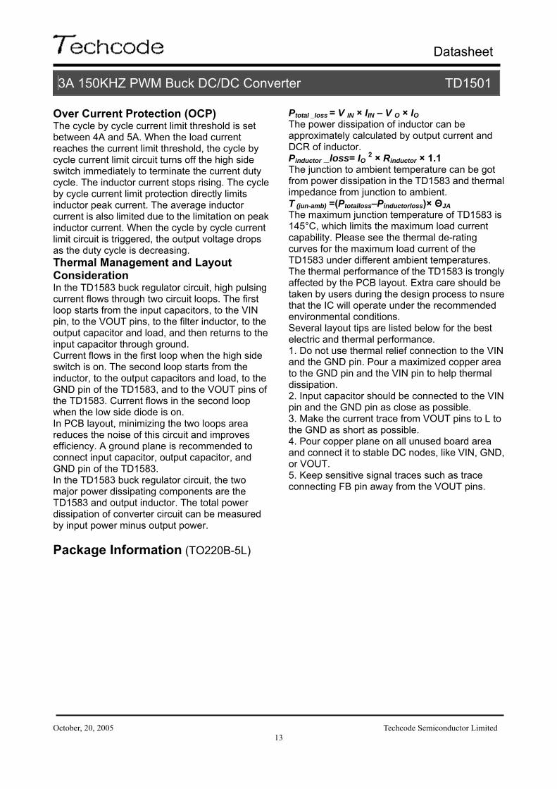
Package Information (TO220B-5L)
Datasheet
3A 150KHZ PWM Buck DC/DC Converter TD1501
October, 20, 2005 Techcode Semiconductor Limited
14
Datasheet
3A 150KHZ PWM Buck DC/DC Converter TD1501
October, 20, 2005 Techcode Semiconductor Limited
15
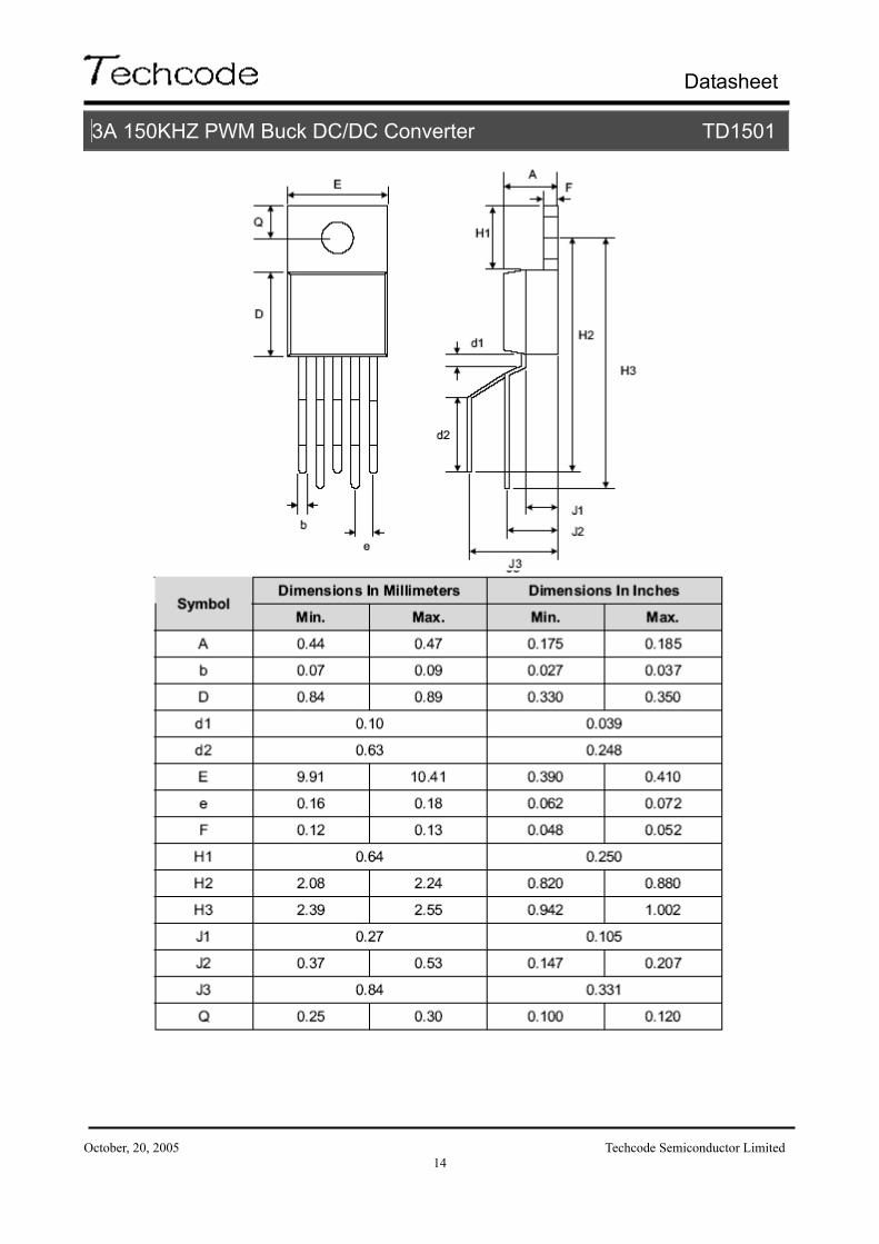
Package Information (TO220-5L)
Datasheet
3A 150KHZ PWM Buck DC/DC Converter TD1501
October, 20, 2005 Techcode Semiconductor Limited
16
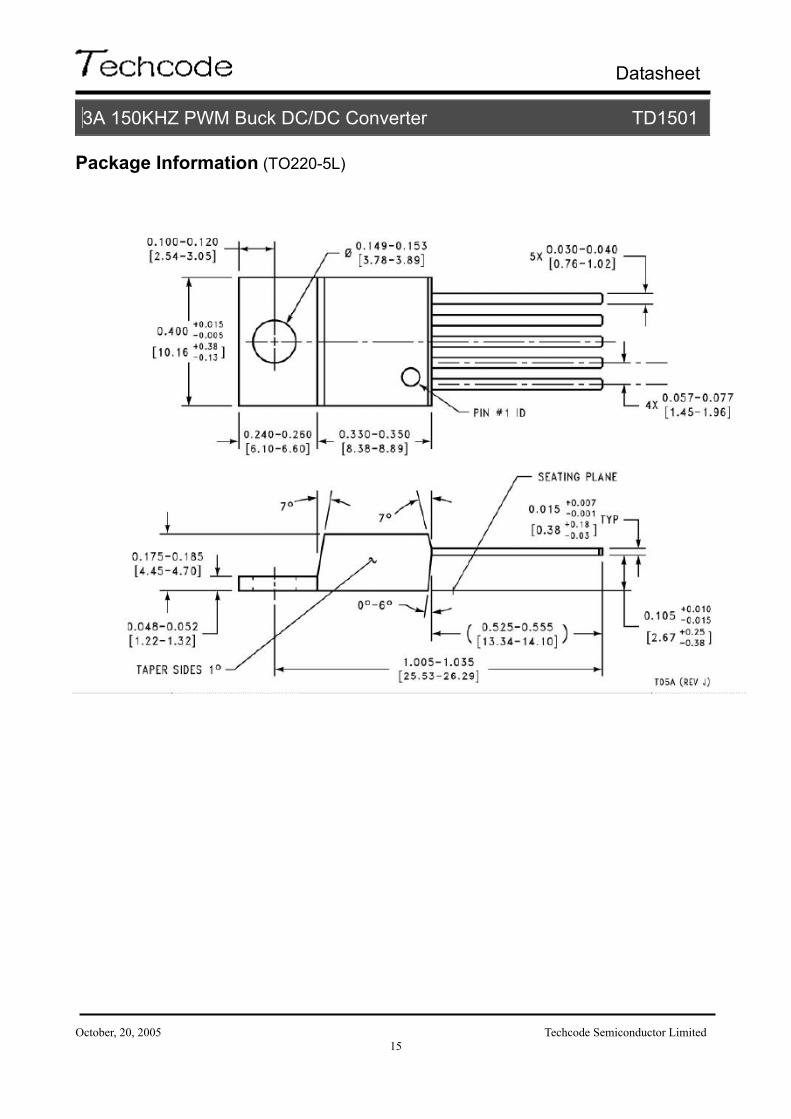
Package Information (TO263-5L)

Datasheet
3A 150KHZ PWM Buck DC/DC Converter TD1501
October, 20, 2005 Techcode Semiconductor Limited
17
Design Notes


![CR-1 : @TAWAS B LIB.TAWAS B(SCH 1):PAGE1 TAWASnotebookschematic.org/data/NOTEBOOK/attachments/SC... · resume gp[6] gp[7] gp[8] gp[9] 3.3v 3.3v 3.3v 3.3v gp[23] gp[24] gp[25] gp[26]](https://img.pdfslide.net/doc/110x75/5f812ff679030c23f20de0bd/cr-1-tawas-b-libtawas-bsch-1page1-ta-resume-gp6-gp7-gp8-gp9-33v.jpg)