Embed Size (px)
Citation preview

COLOR MONITORSERVICE MANUAL
Website:http://biz.LGservice.comE-mail:http://www.LGEservice.com/techsup.html
CAUTIONBEFORE SERVICING THE UNIT, READ THE SAFETY PRECAUTIONS IN THIS MANUAL.
MODEL: T730SH (T730SHM-K***E*)CHASSIS NO. : CA-136
( ) **Same model for Service
*Same looking with new chassis.
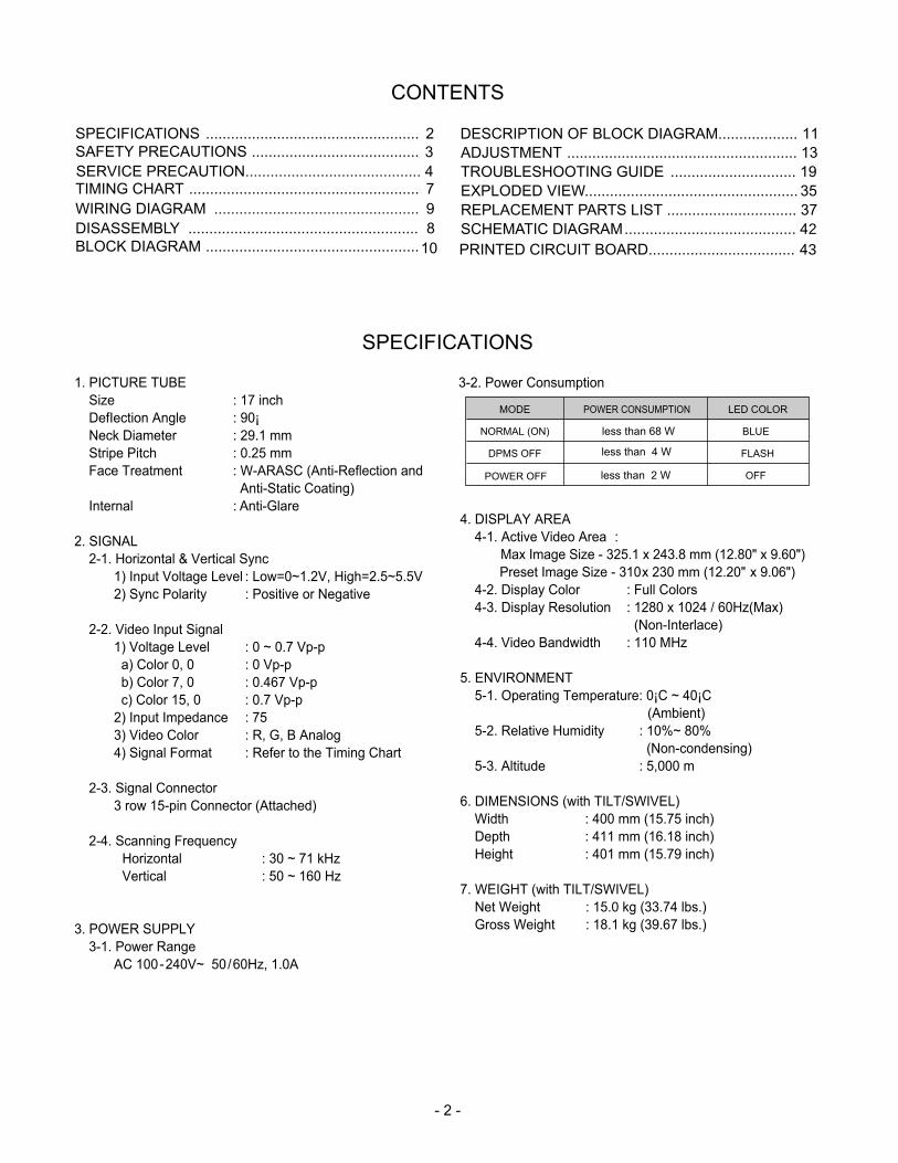
1. PICTURE TUBE Size : 17 inch DefIection Angle : 90¡Neck Diameter : 29.1 mmStripe Pitch : 0.25 mmFace Treatment : W-ARASC (Anti-Reflection and
Anti-Static Coating)Internal : Anti-Glare
2. SIGNAL2-1. Horizontal & Vertical Sync
1) Input Voltage Level : Low=0~1.2V, High=2.5~5.5V2) Sync Polarity : Positive or Negative
2-2. Video Input Signal1) Voltage Level : 0 ~ 0.7 Vp-pa) Color 0, 0 : 0 Vp-pb) Color 7, 0 : 0.467 Vp-pc) Color 15, 0 : 0.7 Vp-p
2) Input Impedance : 75 �3) Video Color : R, G, B Analog4) Signal Format : Refer to the Timing Chart
2-3. Signal Connector3 row 15-pin Connector (Attached)
2-4. Scanning FrequencyHorizontal : 30 ~ 71 kHzVertical : 50 ~ 160 Hz
3. POWER SUPPLY3-1. Power Range
AC 100-240V~ 50/60Hz, 1.0A
3-2. Power Consumption
4. DISPLAY AREA4-1. Active Video Area :
Max Image Size - 325.1 x 243.8 mm (12.80" x 9.60")Preset Image Size - 310 x 230 mm (12.20" x 9.06")
4-2. Display Color : Full Colors4-3. Display Resolution : 1280 x 1024 / 60Hz(Max)
(Non-Interlace)4-4. Video Bandwidth : 110 MHz
5. ENVIRONMENT5-1. Operating Temperature: 0¡C ~ 40¡C
(Ambient)5-2. Relative Humidity : 10%~ 80%
(Non-condensing)5-3. Altitude : 5,000 m
6. DIMENSIONS (with TILT/SWIVEL)Width : 400 mm (15.75 inch)Depth : 411 mm (16.18 inch)Height : 401 mm (15.79 inch)
7. WEIGHT (with TILT/SWIVEL)Net Weight : 15.0 kg (33.74 lbs.)Gross Weight : 18.1 kg (39.67 lbs.)
CONTENTS
- 2 -
SPECIFICATIONS ................................................... 2SAFETY PRECAUTIONS ........................................ 3
TIMING CHART ....................................................... 7WIRING DIAGRAM ................................................. 9DISASSEMBLY ....................................................... 8BLOCK DIAGRAM ................................................... 10
DESCRIPTION OF BLOCK DIAGRAM................... 11ADJUSTMENT ....................................................... 13TROUBLESHOOTING GUIDE .............................. 19EXPLODED VIEW................................................... 35REPLACEMENT PARTS LIST ............................... 37SCHEMATIC DIAGRAM......................................... 42PRINTED CIRCUIT BOARD................................... 43
SPECIFICATIONS
MODE
NORMAL (ON)
DPMS OFF
POWER CONSUMPTION
less than 68 W
less than 4 W
LED COLOR
BLUE
FLASH
SERVICE PRECAUTION.......................................... 4
POWER OFF less than 2 W OFF
SAFETY PRECAUTIONS
- 3 -
SAFETY-RELATED COMPONENT WARNING!There are special components used in this color monitorwhich are important for safety. These parts are marked
on the schematic diagram and the replacementparts list. It is essential that these critical parts should bereplaced with the manufacturer's specified parts to preventX-radiation, shock, fire, or other hazards. Do not modifythe original design without obtaining written permissionfrom manufacturer or you will void the original parts andlabor guarantee.
CAUTION: No modification of any circuit should beattempted.Service work should be performed only afteryou are thoroughly familiar with all of thefollowing safety checks and servicingguidelines.
SAFETY CHECKCare should be taken while servicing this color monitorbecause of the high voltage used in the deflection circuits.These voltages are exposed in such areas as theassociated flyback and yoke circuits.
FIRE & SHOCK HAZARDAn isolation transformer must be inserted between the
color monitor and AC power line before servicing thechassis.
• In servicing, attention must be paid to the original leaddress specially in the high voltage circuit. If a shortcircuit is found, replace all parts which have beenoverheated as a result of the short circuit.
• All the protective devices must be reinstalled per theoriginal design.
• Soldering must be inspected for the cold solder joints,frayed leads, damaged insulation, solder splashes, orthe sharp points. Be sure to remove all foreignmaterials.
IMPLOSION PROTECTIONAll used display tubes are equipped with an integralimplosion protection system, but care should be taken toavoid damage and scratching during installation. Use onlysame type display tubes.
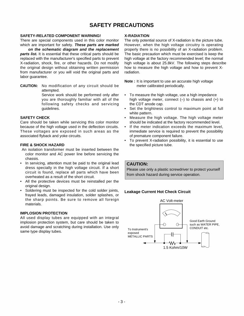
X-RADIATIONThe only potential source of X-radiation is the picture tube.However, when the high voltage circuitry is operatingproperly there is no possibility of an X-radiation problem.The basic precaution which must be exercised is keep thehigh voltage at the factory recommended level; the normalhigh voltage is about 25.8kV. The following steps describehow to measure the high voltage and how to prevent X-radiation.
Note : It is important to use an accurate high voltage meter calibrated periodically.
• To measure the high voltage, use a high impedance high voltage meter, connect (–) to chassis and (+) tothe CDT anode cap.
• Set the brightness control to maximum point at fullwhite pattern.
• Measure the high voltage. The high voltage metershould be indicated at the factory recommended level.
• If the meter indication exceeds the maximum level,immediate service is required to prevent the possibilityof premature component failure.
• To prevent X-radiation possibility, it is essential to usethe specified picture tube.
Leakage Current Hot Check Circuit
CAUTION:Please use only a plastic screwdriver to protect yourselffrom shock hazard during service operation.
1.5 Kohm/10W
To Instrument'sexposed METALLIC PARTS
Good Earth Groundsuch as WATER PIPE,CONDUIT etc.
AC Volt-meter
- 4 -
SERVICING PRECAUTIONSCAUTION: Before servicing receivers covered by thisservice manual and its supplements and addenda, readand follow the SAFETY PRECAUTIONS on page 3 of thispublication.NOTE: If unforeseen circumstances create conflictbetween the following servicing precautions and any of thesafety precautions on page 3 of this publication, alwaysfollow the safety precautions. Remember: Safety First.
General Servicing Precautions1. Always unplug the receiver AC power cord from the AC
power source before;a. Removing or reinstalling any component, circuit
board module or any other receiver assembly.b. Disconnecting or reconnecting any receiver electrical
plug or other electrical connection.c. Connecting a test substitute in parallel with an
electrolytic capacitor in the receiver.CAUTION: A wrong part substitution or incorrectpolarity installation of electrolytic capacitors mayresult in an explosion hazard.
d. Discharging the picture tube anode.2. Test high voltage only by measuring it with an
appropriate high voltage meter or other voltagemeasuring device (DVM, FETVOM, etc) equipped witha suitable high voltage probe.Do not test high voltage by "drawing an arc".
3. Discharge the picture tube anode only by (a) firstconnecting one end of an insulated clip lead to thedegaussing or kine aquadag grounding system shieldat the point where the picture tube socket ground leadis connected, and then (b) touch the other end of theinsulated clip lead to the picture tube anode button,using an insulating handle to avoid personal contactwith high voltage.
4. Do not spray chemicals on or near this receiver or anyof its assemblies.
5. Unless specified otherwise in this service manual,clean electrical contacts only by applying the followingmixture to the contacts with a pipe cleaner, cotton-tipped stick or comparable non-abrasive applicator;10% (by volume) Acetone and 90% (by volume)isopropyl alcohol (90%-99% strength)CAUTION: This is a flammable mixture.Unless specified otherwise in this service manual,lubrication of contacts in not required.
6. Do not defeat any plug/socket B+ voltage interlockswith which receivers covered by this service manualmight be equipped.
7. Do not apply AC power to this instrument and/or any ofits electrical assemblies unless all solid-state deviceheat sinks are correctly installed.
8. Always connect the test receiver ground lead to thereceiver chassis ground before connecting the testreceiver positive lead.Always remove the test receiver ground lead last.
9. Use with this receiver only the test fixtures specified inthis service manual.CAUTION: Do not connect the test fixture ground strapto any heat sink in this receiver.
Electrostatically Sensitive (ES) DevicesSome semiconductor (solid-state) devices can bedamaged easily by static electricity. Such componentscommonly are called Electrostatically Sensitive (ES)Devices. Examples of typical ES devices are integratedcircuits and some field-effect transistors andsemiconductor "chip" components. The followingtechniques should be used to help reduce the incidence ofcomponent damage caused by static by static electricity.1. Immediately before handling any semiconductor
component or semiconductor-equipped assembly, drainoff any electrostatic charge on your body by touching aknown earth ground. Alternatively, obtain and wear acommercially available discharging wrist strap device,which should be removed to prevent potential shockreasons prior to applying power to the unit under test.
2. After removing an electrical assembly equipped withES devices, place the assembly on a conductivesurface such as aluminum foil, to prevent electrostaticcharge buildup or exposure of the assembly.
3. Use only a grounded-tip soldering iron to solder orunsolder ES devices.
4. Use only an anti-static type solder removal device.Some solder removal devices not classified as "anti-static" can generate electrical charges sufficient todamage ES devices.
5. Do not use freon-propelled chemicals. These cangenerate electrical charges sufficient to damage ESdevices.
6. Do not remove a replacement ES device from itsprotective package until immediately before you areready to install it. (Most replacement ES devices arepackaged with leads electrically shorted together byconductive foam, aluminum foil or comparableconductive material).
7. Immediately before removing the protective materialfrom the leads of a replacement ES device, touch theprotective material to the chassis or circuit assemblyinto which the device will be installed.CAUTION: Be sure no power is applied to the chassisor circuit, and observe all other safety precautions.
8. Minimize bodily motions when handling unpackagedreplacement ES devices. (Otherwise harmless motionsuch as the brushing together of your clothes fabric orthe lifting of your foot from a carpeted floor cangenerate static electricity sufficient to damage an ESdevice.)
- 5 -
General Soldering Guidelines1. Use a grounded-tip, low-wattage soldering iron and
appropriate tip size and shape that will maintain tiptemperature within the range or 500 F to 600 F.
2. Use an appropriate gauge of RMA resin-core soldercomposed of 60 parts tin/40 parts lead.
3. Keep the soldering iron tip clean and well tinned.4. Thoroughly clean the surfaces to be soldered. Use a
mall wire-bristle (0.5 inch, or 1.25cm) brush with ametal handle.Do not use freon-propelled spray-on cleaners.
5. Use the following unsoldering techniquea. Allow the soldering iron t ip to reach normal
temperature.(500 F to 600 F)
b. Heat the component lead until the solder melts.c. Quickly draw the melted solder with an anti-static,
suction-type solder removal device or with solderbraid.CAUTION: Work quickly to avoid overheating thecircuitboard printed foil.
6. Use the following soldering technique.a. Allow the soldering iron tip to reach a normal
temperature (500 F to 600 F)b. First, hold the soldering iron tip and solder the strand
against the component lead until the solder melts.
c. Quickly move the soldering iron tip to the junction ofthe component lead and the printed circuit foil, andhold it there only until the solder flows onto andaround both the component lead and the foil.CAUTION: Work quickly to avoid overheating thecircuit board printed foil.
d. Closely inspect the solder area and remove anyexcess or splashed solder with a small wire-bristlebrush.
IC Remove/ReplacementSome chassis circuit boards have slotted holes (oblong)through which the IC leads are inserted and then bent flatagainst the circuit foil. When holes are the slotted type,the following technique should be used to remove andreplace the IC. When working with boards using thefamiliar round hole, use the standard technique asoutlined in paragraphs 5 and 6 above.
Removal1. Desolder and straighten each IC lead in one operation
by gently prying up on the lead with the soldering irontip as the solder melts.
2. Draw away the melted solder with an anti-staticsuction-type solder removal device (or with solderbraid) before removing the IC.
Replacement1. Carefully insert the replacement IC in the circuit board.2. Carefully bend each IC lead against the circuit foil pad
and solder it.3. Clean the soldered areas with a small wire-bristle
brush. (It is not necessary to reapply acrylic coating tothe areas).
"Small-Signal" Discrete TransistorRemoval/Replacement1. Remove the defective transistor by clipping its leads as
close as possible to the component body.2. Bend into a "U" shape the end of each of three leads
remaining on the circuit board.3. Bend into a "U" shape the replacement transistor leads.4. Connect the replacement transistor leads to the
corresponding leads extending from the circuit boardand crimp the "U" with long nose pliers to insure metalto metal contact then solder each connection.
Power Output, Transistor DeviceRemoval/Replacement1. Heat and remove all solder from around the transistor
leads.2. Remove the heat sink mounting screw (if so equipped).3. Carefully remove the transistor from the heat sink of the
circuit board.4. Insert new transistor in the circuit board.5. Solder each transistor lead, and clip off excess lead.6. Replace heat sink.
Diode Removal/Replacement1. Remove defective diode by clipping its leads as close
as possible to diode body.2. Bend the two remaining leads perpendicular y to the
circuit board.3. Observing diode polarity, wrap each lead of the new
diode around the corresponding lead on the circuitboard.
4. Securely crimp each connection and solder it.5. Inspect (on the circuit board copper side) the solder
joints of the two "original" leads. If they are not shiny,reheat them and if necessary, apply additional solder.
Fuse and Conventional ResistorRemoval/Replacement1. Clip each fuse or resistor lead at top of the circuit board
hollow stake.2. Securely crimp the leads of replacement component
around notch at stake top.3. Solder the connections.
CAUTION: Maintain original spacing between thereplaced component and adjacent components and thecircuit board to prevent excessive componenttemperatures.
- 6 -
Circuit Board Foil RepairExcessive heat applied to the copper foil of any printedcircuit board will weaken the adhesive that bonds the foilto the circuit board causing the foil to separate from or"l i f t-off" the board. The following guidelines andprocedures should be followed whenever this condition isencountered.
At IC ConnectionsTo repair a defective copper pattern at IC connections usethe following procedure to install a jumper wire on thecopper pattern side of the circuit board. (Use thistechnique only on IC connections).
1. Carefully remove the damaged copper pattern with asharp knife. (Remove only as much copper asabsolutely necessary).
2. carefully scratch away the solder resist and acryliccoating (if used) from the end of the remaining copperpattern.
3. Bend a small "U" in one end of a small gauge jumperwire and carefully crimp it around the IC pin. Solder theIC connection.
4. Route the jumper wire along the path of the out-awaycopper pattern and let it overlap the previously scrapedend of the good copper pattern. Solder the overlappedarea and clip off any excess jumper wire.
At Other ConnectionsUse the following technique to repair the defective copperpattern at connections other than IC Pins. This techniqueinvolves the installation of a jumper wire on thecomponent side of the circuit board.1. Remove the defective copper pattern with a sharp
knife.Remove at least 1/4 inch of copper, to ensure that ahazardous condition will not exist if the jumper wireopens.
2. Trace along the copper pattern from both sides of thepattern break and locate the nearest component that isdirectly connected to the affected copper pattern.
3. Connect insulated 20-gauge jumper wire from the leadof the nearest component on one side of the patternbreak to the lead of the nearest component on theother side.Carefully crimp and solder the connections.CAUTION: Be sure the insulated jumper wire isdressed so the it does not touch components or sharpedges.
- 7 -
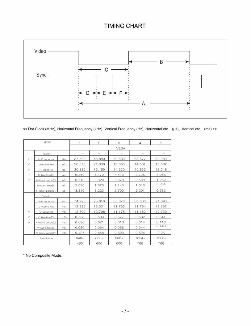
TIMING CHART
* No Composite Mode.
<< Dot Clock (MHz), Horizontal Frequency (kHz), Vertical Frequency (Hz), Horizontal etc... (µs), Vertical etc... (ms) >>
A
BC
D E F
Video
Sync
MODE 1 2 3 4 5
Polarity - + + + +
H H-Frequency KHz 37.500 46.880 53.680 68.677 60.289
O H-Active (A) uS 26.670 21.330 18.630 14.561 16.587
R H-Video(B) uS 20.320 16.160 14.220 10.836 12.518
I H-blanking(C) uS 6.350 5.170 4.410 3.725 4.068
Z H-front porch(D) uS 0.510 0.320 0.570 0.508 1.252
H-sync time(E) uS 2.030 1.620 1.140 1.016 2.034
H-back porch(F) us 3.810 3.223 2.700 2.201 0.782
Polarity - + + + +
V-Frequency Hz 74.990 75.010 85.070 85.000 74.893
V-Active (A) mS 13.335 13.331 11.755 11.764 13.352
V V-Video(B) mS 12.802 12.798 11.178 11.182 12.739
E V-blanking(C) mS 0.533 0.533 0.577 0.582 0.641
R V-front porch(D) mS 0.026 0.021 0.018 0.014 0.116
T V-sync time(E) mS 0.080 0.064 0.056 0.044 0.448
V-back porch(F) mS 0.427 0.448 0.503 0.524 0.05
Resolution 640* 800* 800* 1024* 1280*
480 600 600 768 768
VESA
- 8 -
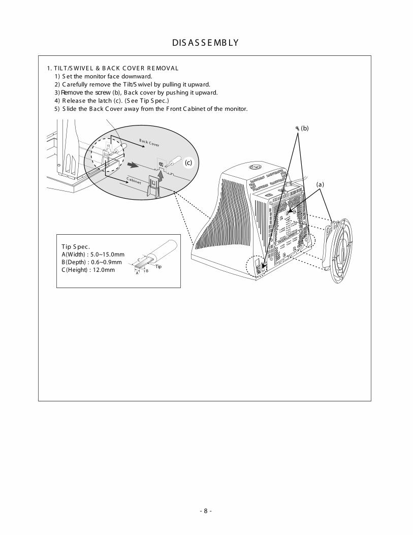
DIS A S S E MB LY
1. T IL T /S WIV E L & B A C K C OV E R R E MOV A L1) S et the monitor face downward.2) C arefully remove the T ilt/S wivel by pulling it upward.3) Remove the screw (b), B ack cover by pushing it upward. 4) R elease the latch (c). (S ee T ip S pec.)5) S lide the B ack C over away from the F ront C abinet of the monitor.
Tip
C
BA
T ip S pec .A(Width) : 5.0~15.0mmB (Depth) : 0.6~0.9mmC (Height) : 12.0mm
(a)
B ack C over
C abinet
(c)
(b)
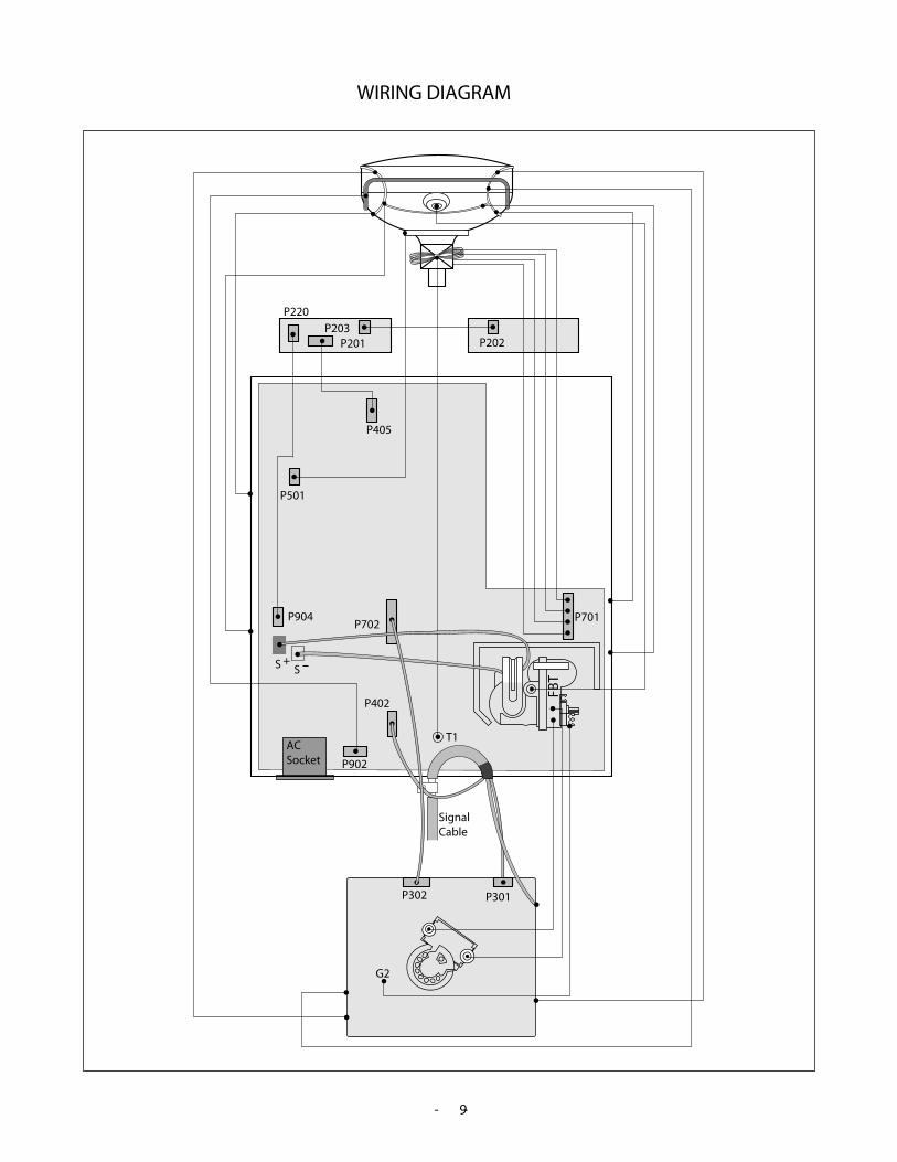
WIRING DIAGRAM
- 9 -
P501
P201
P405
P301P302
G2
P702P701
T1
P402
P902
S +S
Signal Cable
AC Socket
FBT
P203P202
P220
P904
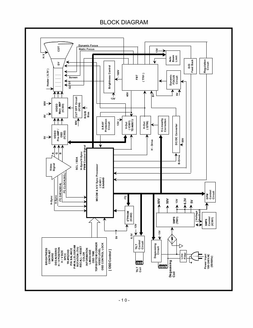
BLOCK DIAGRAM
- 1 0 -
Pow
er In
put
100~
240V
AC(5
0/60
Hz)Line
Filte
r
Deg
auss
ing
Cir
cuit
[ OSD
Con
trol ]
SMPS
Con
trol
(IC90
1)
TILT
Con
trol
Cir
cuit
6.3V
E2PR
OM
(IC40
2)
5V
H-S
ync
V-Sy
nc
I2C
DAT
A(SD
A)I2 C
CLO
CK
(SCL
)
VID
EOPr
e-AM
P /
OSD
(IC30
2)
Vide
oSi
gnal
R G BVI
DEO
Mai
n AM
P(IC
303)
CU
T O
FF C
ircu
it(IC
304)
80V
MIC
OM
& H
/V S
ync
Proc
esso
r( I
C40
1 )
SAA
4849
V-O
ut( I
C60
1)TD
A486
7J
H-O
ut( Q
706)
H-L
inea
rity
Cor
rect
ion
X-R
AYPr
otec
tion
Cir
cuit
Dyn
amic
FOC
US
Cir
cuit
Bri
ghtn
ess
Con
trol
-160
V
40V
D/D
Feed
Bac
k
SCL
/ SD
A
H-S
ync/
V-Sy
ncPW
M C
ontr
ol S
igna
l
50V
DY
CD
T
Hea
ter
( 6.3
V )
I2C
Screen
H.V
R/G
/B
Bia
s
H -
Driv
e
B-D
rive
B+
DPM
Con
trol
Cir
cuit
5V
6.3V
8V
80V
Volta
gefe
edba
ck
Dega
ussi
ngC
oil
Dynamic FocusStatic Focus
TILT
Coi
l
50V
80V
5V
G2
G1
Auto
Bea
mLi
mit
DC
/DC
Con
vert
er
FBT
( T70
1 ) R
egul
atio
nC
ircu
it
SMPS
(T90
1)
5V
BR
IGH
TNES
SC
ON
TRAS
TM
OIR
E D
EGAU
SSIN
GH
/ V
POSI
TIO
NH
/ V
SIZE
SPC
CTR
APEZ
OID
PIN
BAL
ANC
EP
ARAL
LELO
GR
AMR
OTA
TIO
N (T
ilt)
REC
ALL
/ RES
ETC
OLO
RIN
FOR
MAT
ION
LAN
GU
AGE
OSD
TIM
ETO
P/B
OTT
OM
CO
RN
ERVI
DEO
LEV
ELO
SD C
ON
TRO
L LO
CK
13V
13V
13V
13V
13V
13V
DESCRIPTION OF BLOCK DIAGRAM
- 11 -
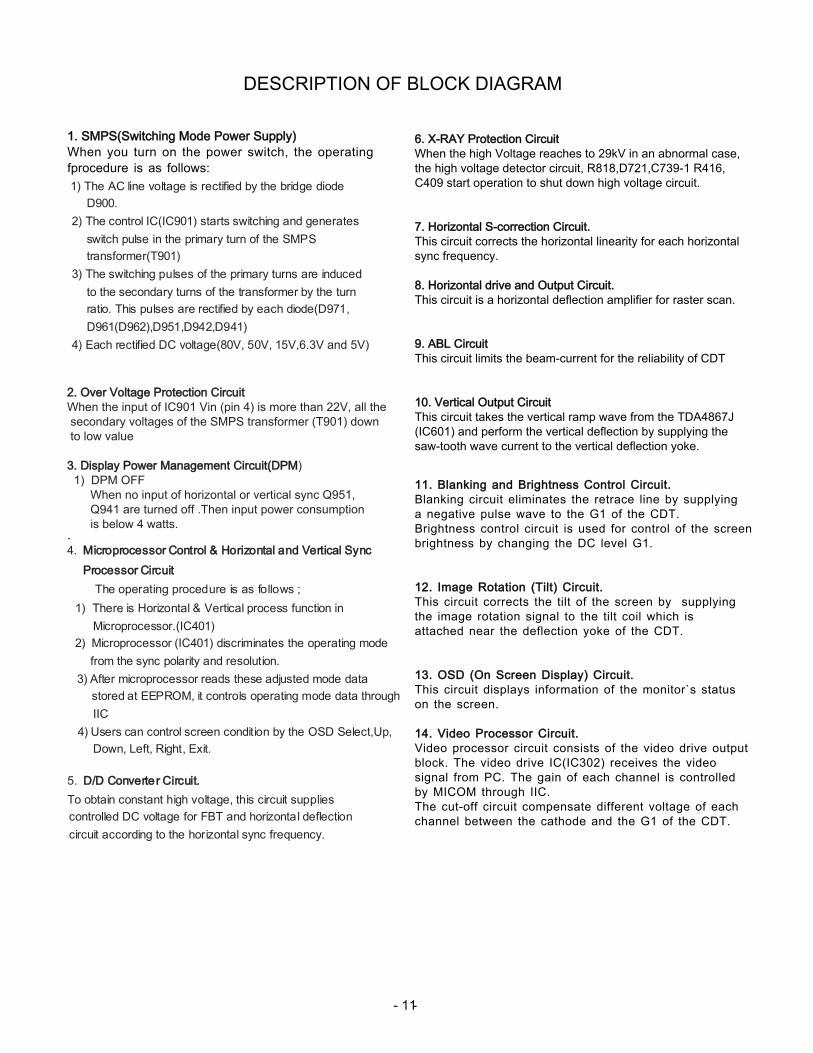
1. SMPS(Switching Mode Power Supply)When you turn on the power switch, the operatingfprocedure is as follows:
.
6. X-RAY Protection CircuitWhen the high Voltage reaches to 29kV in an abnormal case,the high voltage detector circuit, R818,D721,C739-1 R416,C409 start operation to shut down high voltage circuit.
7. Horizontal S-correction Circuit.This circuit corrects the horizontal linearity for each horizontalsync frequency.
8. Horizontal drive and Output Circuit.This circuit is a horizontal deflection amplifier for raster scan.
9. ABL CircuitThis circuit limits the beam-current for the reliability of CDT
10. Vertical Output CircuitThis circuit takes the vertical ramp wave from the TDA4867J (IC601) and perform the vertical deflection by supplying thesaw-tooth wave current to the vertical deflection yoke.
11. Blanking and Brightness Control Circuit.Blanking circuit eliminates the retrace line by supplying a negative pulse wave to the G1 of the CDT.Brightness control circuit is used for control of the screen brightness by changing the DC level G1.
12. Image Rotation (Tilt) Circuit.This circuit corrects the tilt of the screen by supplying the image rotation signal to the tilt coil which isattached near the deflection yoke of the CDT.
13. OSD (On Screen Display) Circuit.This circuit displays information of the monitor`s statuson the screen.
14. Video Processor Circuit.Video processor circuit consists of the video drive outputblock. The video drive IC(IC302) receives the video signal from PC. The gain of each channel is controlled by MICOM through IIC.The cut-off circuit compensate different voltage of each channel between the cathode and the G1 of the CDT.
1) The AC line voltage is rectified by the bridge diodeD900.
2) The control IC(IC901) starts switching and generatesswitch pulse in the primary turn of the SMPStransformer(T901)
3) The switching pulses of the primary turns are inducedto the secondary turns of the transformer by the turn ratio. This pulses are rectified by each diode(D971,D961(D962),D951,D942,D941)
4) Each rectified DC voltage(80V, 50V, 15V,6.3V and 5V)
2. Over Voltage Protection CircuitWhen the input of IC901 Vin (pin 4) is more than 22V, all the secondary voltages of the SMPS transformer (T901) down to low value
3. Display Power Management Circuit(DPM) 1) DPM OFF When no input of horizontal or vertical sync Q951, Q941 are turned off .Then input power consumption is below 4 watts. 4. Microprocessor Control & Horizontal and Vertical Sync
Processor CircuitThe operating procedure is as follows ;
1) There is Horizontal & Vertical process function in Microprocessor.(IC401)
2) Microprocessor (IC401) discriminates the operating modefrom the sync polarity and resolution.
3) After microprocessor reads these adjusted mode datastored at EEPROM, it controls operating mode data throughIIC
4) Users can control screen condition by the OSD Select,Up, Down, Left, Right, Exit.
5. D/D Converte r Circuit.To obtain constant high voltage, this circuit suppliescontrolled DC voltage for FBT and horizontal deflectioncircuit according to the horizontal sync frequency.

- 12 -
15. Video Pre-Amp Circuit.This circuit amplifies the analog video signal from 0~0.7 V to 0~4 V. It is operated by taking the clamp, R,G,B drive and contrast signal from the MICOM (IC401)
16. Video Output Amp Circuit.This circuit amplifies the video signal which comes from thevideo pre-amp circuit and amplified it to applied the CDTcathode
1. Preparation for Service Adjustment
GENERAL INFORMATION
All adjustment are thoroughly checked and correctedwhen the monitor leaves the factory, but sometimesseveral adjustments may be required. Adjustment should be following procedure and afterwarming up for a minimum of 30 minutes.
• Alignment appliances and tools.- IBM compatible PC.- Programmable Signal Generator. (eg. VG-819 made by Astrodesign Co.)
- EPROM or EEPROM with saved each mode data.- Alignment Adaptor and Software.- Digital Voltmeter.- White Balance Meter.- Luminance Meter.- High-voltage Meter.
AUTOMATIC AND MANUAL DEGAUSSINGThe degaussing coil is mounted around the CDT so thatautomatic degaussing when turn on the monitor. But amonitor is moved or faced in a different direction, becomepoor color purity cause of CDT magnetized, then pressDEGAUSSING on the OSD menu.
ADJUSTMENT PROCEDURE & METHOD
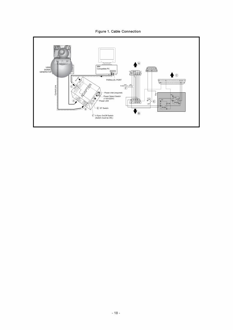
- Install the cable for adjustment such as Figure 1and runthe alignment program on the DOS for IBMcompatible PC.
- Set external Brightness and Contrast volume to maxposition.
1. Adjustment for B+ Voltage.
1) Display cross hatch pattern at Mode 4.2) Check D961 cathode voltage within 50V ± 1V .
2. Adjustment for High-Voltage.
1) Display cross hatch pattern at Mode 4.2) Enter the SVC SUB menu as the following instruction.3) Adjust H/Voltage to 25.8kV±0.1 kV by adjust 1-P value.
2. Adjustment by Service Hot key
How to enter SVC HOT KEY1. Press Menu and OSD window will appear.2. While OSD window is displayed, is seen on the
left bottom of OSD window. 3. Press + power switch simultaneously and the
screen will immediately refresh. 4. Press Menu and make sure that is changed to
1 2.5. Follow the menu on the left of OSD window to find 12
and OSD will change as shown in the figure.6. Select Degauss in the above figure and then press
Select and to enter the screen of the SUB menu. (Back Raster for Pattern)
FOS SPEC
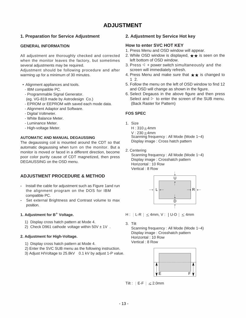
1. SizeH : 310 4mmV : 230 4mmScanning frequency : All Mode (Mode 1~4)Display image : Cross hatch pattern
2. CenteringScanning frequency : All Mode (Mode 1~4)Display image : Crosshatch patternHorizontal : 10 RowVertical : 8 Row
H : L-R 4mm, V : U-D 4mm
3. TiltScanning frequency : All Mode (Mode 1~4)Display image : Crosshatch patternHorizontal : 10 RowVertical : 8 Row
Tilt : E-F 2.0mm
- 13 -
ADJUSTMENT
U
D
L R
E F
- 14 -
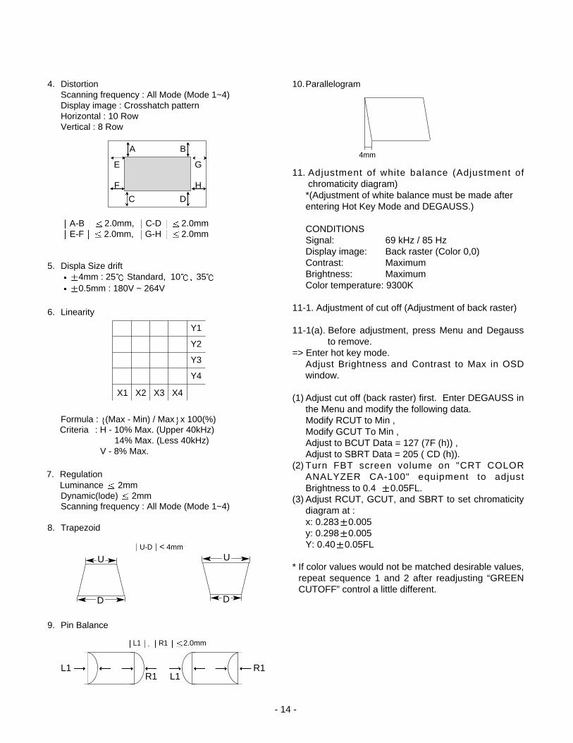
4. DistortionScanning frequency : All Mode (Mode 1~4)Display image : Crosshatch patternHorizontal : 10 RowVertical : 8 Row
A-B 2.0mm, C-D 2.0mmE-F 2.0mm, G-H 2.0mm
5. Displa Size drift4mm : 25 Standard, 10 350.5mm : 180V ~ 264V
6. Linearity
Formula : (Max - Min) / Max x 100(%)Criteria : H - 10% Max. (Upper 40kHz)
14% Max. (Less 40kHz)V - 8% Max.
7. RegulationLuminance 2mmDynamic(lode) 2mmScanning frequency : All Mode (Mode 1~4)
8. Trapezoid
9. Pin Balance
10.Parallelogram
11. Adjustment of white balance (Adjustment ofchromaticity diagram)*(Adjustment of white balance must be made after entering Hot Key Mode and DEGAUSS.)
CONDITIONSSignal: 69 kHz / 85 HzDisplay image: Back raster (Color 0,0)Contrast: MaximumBrightness: MaximumColor temperature: 9300K
11-1. Adjustment of cut off (Adjustment of back raster)
11-1(a). Before adjustment, press Menu and Degaussto remove.
=> Enter hot key mode.Adjust Brightness and Contrast to Max in OSDwindow.
(1) Adjust cut off (back raster) first. Enter DEGAUSS inthe Menu and modify the following data.Modify RCUT to Min , Modify GCUT To Min , Adjust to BCUT Data = 127 (7F (h)) ,Adjust to SBRT Data = 205 ( CD (h)).
(2) Turn FBT screen volume on "CRT COLORANALYZER CA-100" equipment to adjustBrightness to 0.4 0.05FL.
(3) Adjust RCUT, GCUT, and SBRT to set chromaticitydiagram at :x: 0.283 0.005 y: 0.298 0.005 Y: 0.40 0.05FL
* If color values would not be matched desirable values,repeat sequence 1 and 2 after readjusting “GREENCUTOFF” control a little different.
U
D D
UU-D < 4mm
L1 R1 2.0mm
L1 R1 L1
R1
Y1
Y2
Y3
Y4
X1 X2 X3 X4
4mmA B
DC
E G
F H
11-2. Adjustment of White Balance After finishing adjustment of cut off (back raster),approve "Color(15.0) Full white pattern".Adjust BDRV Data = 85 SCON=127.Adjust RDRV and GDRV to set chromaticity diagram at : x: 0.283 0.005 y: 0.298 0.005 Approve "Window pattern (70x70mm)" to adjust S-CON to Y : 50 1FL.Approve "Color (15.0) Full white pattern" again andadjust ABL Data to Y : 32 1FL
12. Focus Adjustment
CONDITIONSScanning frequency : All Mode (Mode 1~4)Display image: "H" character patternBrightness: Cut off pointContrast: Maximum
PROCEDURE1. Adjust the Focus VR on the FBT to display the
sharpest image possible.2. Use Locktite to seal the Focus VR in position.
13. Color Purity AdjustmentColor purity is the absence of undesired color.Conspicuous mislanding (unexpected color in a uniformfield) within the display area shall not be visible at adistance of 50 cm from the CRT surface.
CONDITIONSOrientation: Monitor facing eastScanning Frequency: 1024 x 768@85Hz(69kHz/85Hz)Display image: White flat fieldLuminance: Cut off point at the center of the
display area
Note: Color purity adjustments should only beattempted by qualified personnel.
PROCEDUREFor trained and experienced service technicians only.Use the following procedure to correct minor colorpurity problems:
1. Make sure the display is not affected by externalmagnetic fields.
2. Very carefully break the glue seal between the 2-polepurity convergence magnets (PCM), the band andthe spacer.
3. Make sure the spacing between the PCM assemblyand the CRT stem is 29 mm 1 mm.
4. Display a green pattern over the entire display area.
5. Adjust the purity magnet rings on the PCM assemblyto display a pure green pattern.(Optimum setting: x = 0.295 0.015,y = 0.594 0.015)
6. Repeat steps 4 and 5 using a red pattern and thenagain, using a blue pattern.
Table 4-6. Color Purity Tolerances
(For 9300K color adjustment: x = 0.283 0.02, y = 0.298 0.02)
7. When you have the PCMs properly adjusted,carefully glue them together to prevent theirmovement during shipping.
- 15 -
Red: x=0.620 0.015 y=0.334 0.015
Green: x=0.620 0.015 y=0.334 0.015
Blue: x=0.620 0.015 y=0.334 0.015

- 16 -
3. Adjustment Using Service software Program(Adjustment Program)
1. Adjustment for Factory Mode (Preset Mode).
1) Display cross hatch pattern at Mode All.2) Run alignment program for T730SHM on
the IBM compatible PC.3) EEPROM → ALL CLEAR → Y(Yes) command.
<Caution> Do not run this procedure unless the EEPROM is changed. All data in EEPROM (mode data and color data) will be erased.
4) COMMAND → PRESET START → Y(Yes)command.
5) DIST. ADJ. → FOS. ADJ command. 6) Adjust H-POSITION as arrow keys to center of the
screen.7) Adjust H-SIZE as arrow keys to 310 ± 2mm.8) Adjust V-POSITION as arrow keys to center of the
screen.9) Adjust V-SIZE as arrow keys to 230 ± 2mm.10) Adjust TRAPEZOID as arrow keys to be the best
condition.11) Adjust SIDE PINCUSHON as arrow keys to be the
best condition.12) Adjust TILT as arrow keys to be the best condition.13) Display cross hatch pattern at Mode 4.14) DIST. ADJ. → BALANCE DATA command.15) Adjust balance of Pin-Balance as arrow keys to be
the best condition. 16) Adjust parallelogram as arrow keys to be the best
condition.17) Save of the Mode.18) Save of the System.19) Display from Mode 4 and repeat above from number
6) to 16).20) COMMAND → PRESET EXIT → Y (Yes) command.
2. Adjustment for White Balance and Luminance.
1) Set the White Balance Meter.2) Press the DEGAUSSING on the OSD menu for
demagnetization of the CDT.3) Display color 0,0 pattern at Mode 4.4) COMMAND → PRESET START → Y(Yes)
command.5) Set Bightness and Contrast to max position.6) COLOR ADJ. → LUMINANCE command of the
alignment program.7) COLOR ADJ. → BIAS ADJ. command of the
alignment program.8) Check whether blue color or not at R-BIAS and G-
BIAS to min posit ion, Sub-Brightness to 205(CD(h))position, B-Bias to 127(7F(h))position. If it's notblue color, the monitor must repair.
9) Adjust Screen control on the FBT to 0.4 ± 0.05FLof the raster luminance.
10) Adjust R-BIAS and G-BIAS command to x=0.283 ±0.006 and y=0.298 ± 0.006 on the White BalanceMeter with PC arrow keys.
11) Display color 15,0 Full White(70x70mm) at mode 4.12) DRIVE ADJ command.13) Set B-DRIVE to 85(55(h) at DRIVE of the alignment
program.14) Adjust R-DRIVE and G-DRIVE command to white
balance x=0.283 ± 0.003 and y=0.298 ± 0.003 onthe White Balance Meter with PC arrow keys.
15) Adjust SUB-CONTRAST command to 50±1FL of theraster luminance.
16) Display color 15,0 full white patten at Mode 4.17) COLOR ADJ. → LUMINANCE → ABL command.18) Adjust ABL to 32 ± 1FL of the luminance.19) Exit from the program.
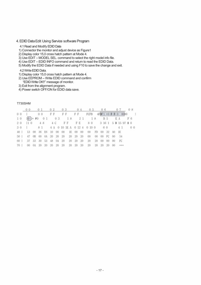
4. EDID Data Edit Using Service software Program 4.1 Read and Modify EDID Data
1) Connector the monitor and adjust device as Figure1 2) Display color 15,0 cross hatch pattern at Mode 4. 3) Use EDIT – MODEL SEL. command to select the right model info file. 4) Use EDIT – EDID INFO command and return to read the EDID Data. 5) Modify the EDID Data if needed and using F10 to save the change and exit. 4.2 Write EDID Data.
1) Display color 15,0 cross hatch pattern at Mode 4. 2) Use EEPROM -- Write EDID command and confirm
“EDID Write OK!!” message of monitor. 3) Exit from the alignment program. 4) Power switch OFF/ON for EDID data save.
- 17 -
T730SHM
00 01 02 03 04 05 06 07 08 09 0A 0B 0C 0D 0E 0F
00 | 00 FF FF FF FF FF FF 00 1E 6D CB 43 *01 00 00 00
10 | **01 0F 01 03 18 21 18 B5 EA F6 29 A2 53 47 99 25
20 | 10 48 4C FF FE 80 31 59 71 4F 45 59 61 59 81 80
30 | 81 4A 01 01 01 01 EA 24 00 60 41 00 28 30 30 60
40 | 13 00 36 E6 10 00 00 1E 00 00 00 FD 00 32 A0 1E
50 | 47 0B 00 0A 20 20 20 20 20 20 00 00 00 FC 00 54
60 | 37 33 30 53 48 0A 20 20 20 20 20 20 00 00 00 FC
70 | 00 0A 20 20 20 20 20 20 20 20 20 20 20 20 00 ***
- 18 -
- 18 -
220
IBMCompatible PC
PARALLEL PORT
Power inlet (required)
Power LED
ST Switch
Power Select Switch(110V/220V)
Con
trol L
ine
Not us
edRS2
32C
PARAL
LEL
V-SYN
CPO
WER
ST
VGS
MONITOR
E
V-Sync On/Off Switch(Switch must be ON.)
F
A
B
C
E
F
A
B
C
15105
569
1
1
114
1325
6
5V
5V
5V
4.7K4.7K
4.7K
74LS06
74LS06
OFF ON
OFF
ON
11
VIDEOSIGNAL
GENERATOR
Figure 1. Cable Connection Figure 1. Cable Connection
1 2
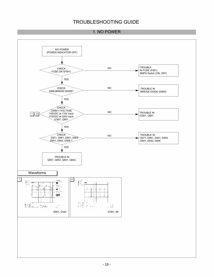
CHECK D900 BRIDGE DIODE?
CHECKC908(+) VOLTAGE
145VDC at 110V input310VDC at 220V input
IC901, Q901
CHECKD971, D961, D951, D904
D941, D942, D906 ?
CHECKFUSE OK?(F901)
- 19 -
TROUBLESHOOTING GUIDE
1. NO POWER
NO POWER(POWER INDICATOR OFF)
NO
NO
NO
NO
TROUBLE IN Q951, Q952, Q941, Q942,
TROUBLE IN FUSE (F901)SMPS Switch (ON, OFF)
Waveforms
TROUBLE INBRIDGE DIODE (D900)
TROUBLE IN IC901, Q901
TROUBLE IN D971, D961, D951, D904D941, D942, D906
YES
YES
YES
YES
Q901, Drain IC901, #6
21
26
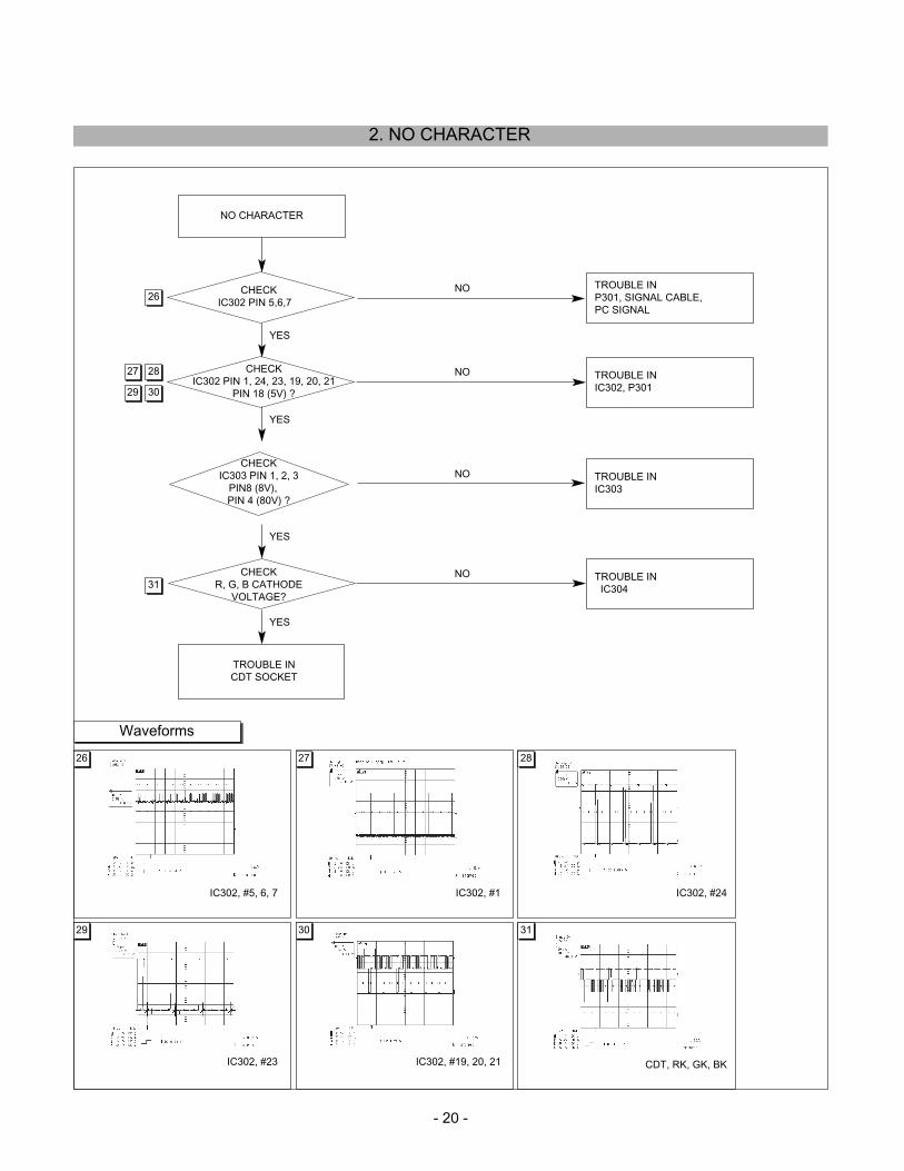
2. NO CHARACTER
NO CHARACTER
NO
NO
NO
NO
TROUBLE IN CDT SOCKET
TROUBLE INP301, SIGNAL CABLE,PC SIGNAL
TROUBLE INIC302, P301
TROUBLE INIC303
TROUBLE INIC304
YES
YES
YES
YES
- 20 -
CHECKIC302 PIN 5,6,7
CHECK IC302 PIN 1, 24, 23, 19, 20, 21
PIN 18 (5V) ?
CHECK IC303 PIN 1, 2, 3
PIN8 (8V), PIN 4 (80V) ?
CHECK R, G, B CATHODE
VOLTAGE?
IC302, #5, 6, 7
IC302, #23 IC302, #19, 20, 21
IC302, #1 IC302, #24
CDT, RK, GK, BK
Waveforms
2827
30
31
26 27 28
29 30 31
29
CHECKSCREEN CONTROL
KNOB OF FBT
CHECK VOLTAGE AT
D961 CATHODE (50V)D971 CATHODE (80V)D951 CATHODE (13V)
D941 CATHODE(6.3V)?
CHECKIC401 (MICOM) PIN 165V (HIGH), IC401 PIN 18
PIN20, PIN21
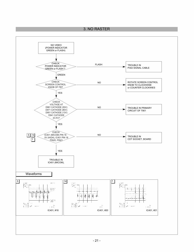
CHECK POWER INDICATORGREEN or FLASH ?
- 21 -
3. NO RASTER
FLASH
NO
NO
NO
TROUBLE INIC401 (MICOM),
TROUBLE IN P302 SIGNAL CABLE
ROTATE SCREEN CONTROLKNOB TO CLOCKWISE or COUNTER CLOCKWIES
TROUBLE IN PRIMARY CIRCUIT OF T901
TROUBLE INCDT SOCKET, BOARD
GREEN
YES
YES
YES
NO VIDEO(POWER INDICATOR GREEN or FLASH)
IC401, #18 IC401, #20 IC401, #21
14
7
5
5 14 7
Waveforms
CHECK IC601 PIN 7 (45V)?
CHECK IC401 PIN 33, 34
(SAWTOOTH WAVE)?
CHECKIC601 Pin 3 (13V) ?
- 22 -
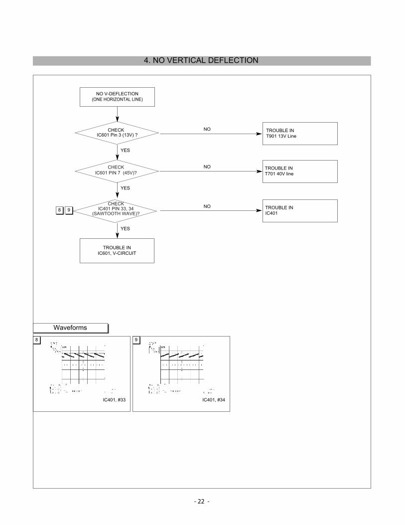
4. NO VERTICAL DEFLECTION
NO V-DEFLECTION(ONE HORIZONTAL LINE)
NO
NO
NO
TROUBLE INIC601, V-CIRCUIT
TROUBLE IN T901 13V Line
Waveforms
TROUBLE INT701 40V line
TROUBLE INIC401
YES
YES
YES
IC401, #33 IC401, #34
98
8 9
3
CHECK IC401 PIN 45, 46
WAVEFORM?
CHECK IC401 PIN , 50 ?
CHECK Q941,Q951
CHECK IC401 (MICOM)
PIN 52, 53 (H/V INPUT) SIGNAL?
- 23 -
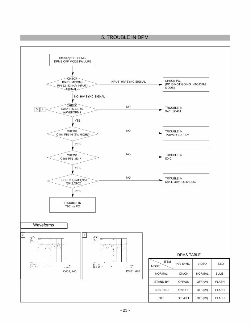
5. TROUBLE IN DPM
4
Stand-by/SUSPEND/DPMS OFF MODE FAILURE
INPUT H/V SYNC SIGNAL
NO
NO
NO
TROUBLE IN T901 or PC
CHECK PC,(PC IS NOT GOING INTO DPMMODE)
TROUBLE INX401, IC401
TROUBLE INPOWER SUPPLY
TROUBLE INIC401
NO TROUBLE INQ941, Q951,Q942,Q952
NO H/V SYNC SIGNAL
YES
YES
YES
YES
DPMS TABLE
NORMAL ON/ON NORMAL BLUE
STAND-BY OFF/ON OFF(0V) FLASH
SUSPEND ON/OFF OFF(0V) FLASH
OFF OFF/OFF OFF(0V) FLASH
H/V SYNC VIDEO LEDMODE
ITEM
C401, #45 IC401, #46
CHECK IC401 PIN 16 (5V, HIGH)?
43
Waveforms
Q942,Q952
CHECK Q953 COLLECTOR VOLTAGE (0.5V)?
CHECK P902?
CHECK RL901?
CHECK IC401 PIN 4 (5V)?
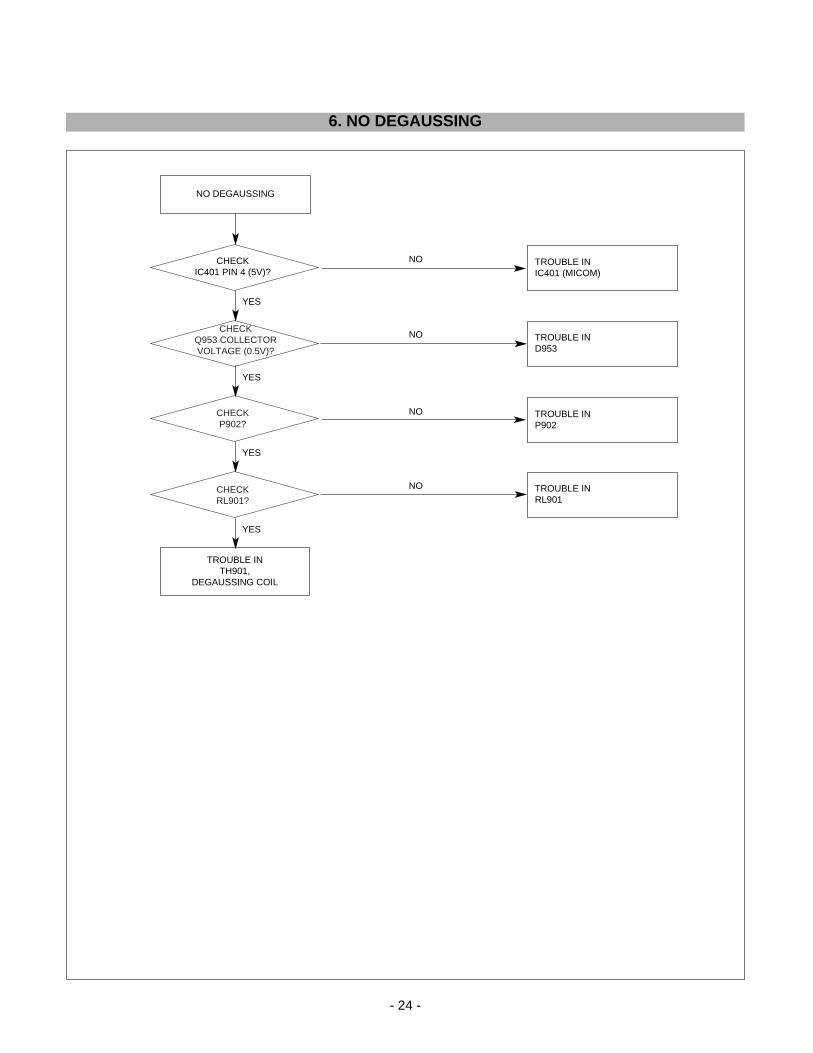
6. NO DEGAUSSING
NO DEGAUSSING
NO
NO
NO
NO
TROUBLE IN TH901,
DEGAUSSING COIL
TROUBLE IN IC401 (MICOM)
TROUBLE IND953
TROUBLE INP902
TROUBLE INRL901
YES
YES
YES
YES
- 24 -
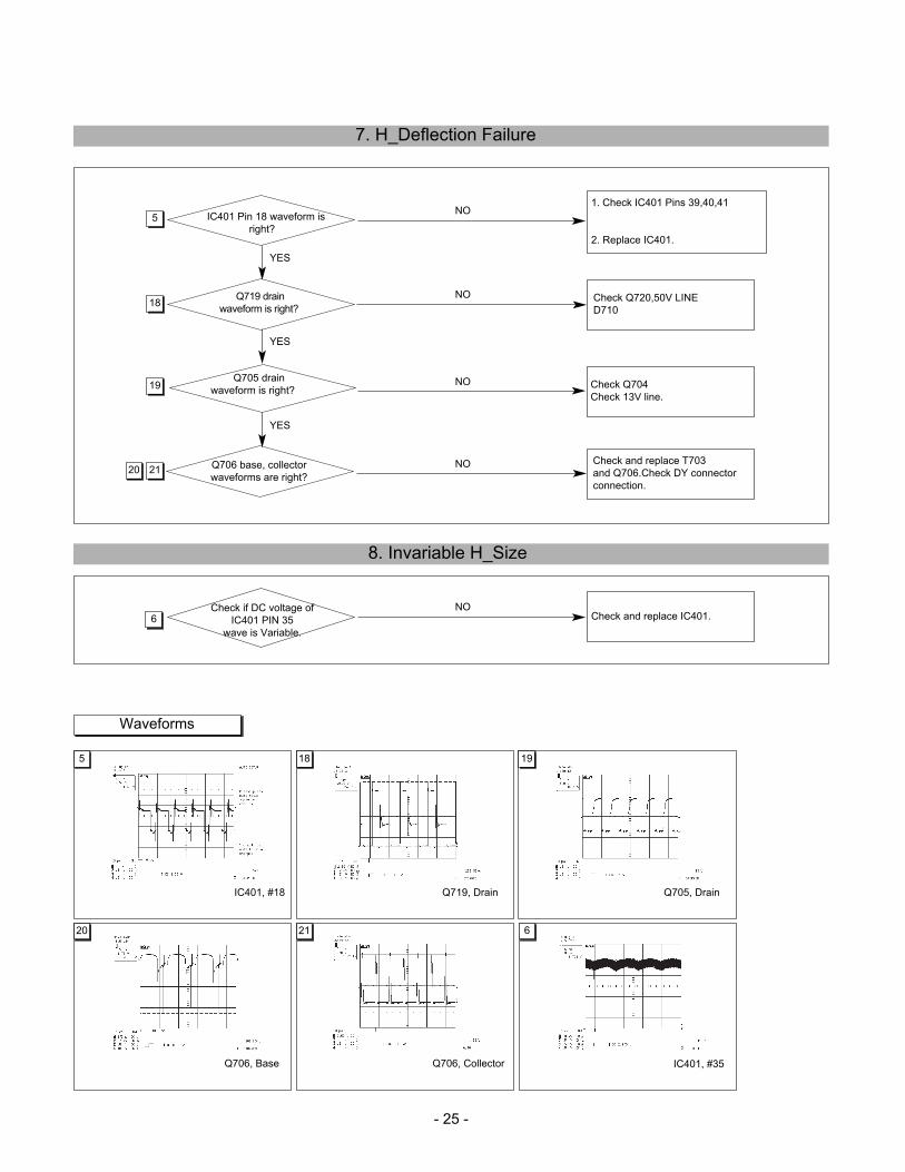
5 18
20 21
19
Q705 drainwaveform is right?
Q706 base, collectorwaveforms are right?
Q719 drain waveform is right?
IC401 Pin 18 waveform isright?
- 25 -
7. H_Deflection Failure
NO
NO
NO
NO
1. Check IC401 Pins 39,40,41
2. Replace IC401.
Check Q720,50V LINED710
Check Q704Check 13V line.
Check and replace T703and Q706.Check DY connectorconnection.
YES
YES
YES
IC401, #18
Q706, Base Q706, Collector
Q719, Drain Q705, Drain
5
18
19
2120
Waveforms
8. Invariable H_Size
NOCheck and replace IC401.
Check if DC voltage of IC401 PIN 35
wave is Variable.6
IC401, #35
6
- 26 -
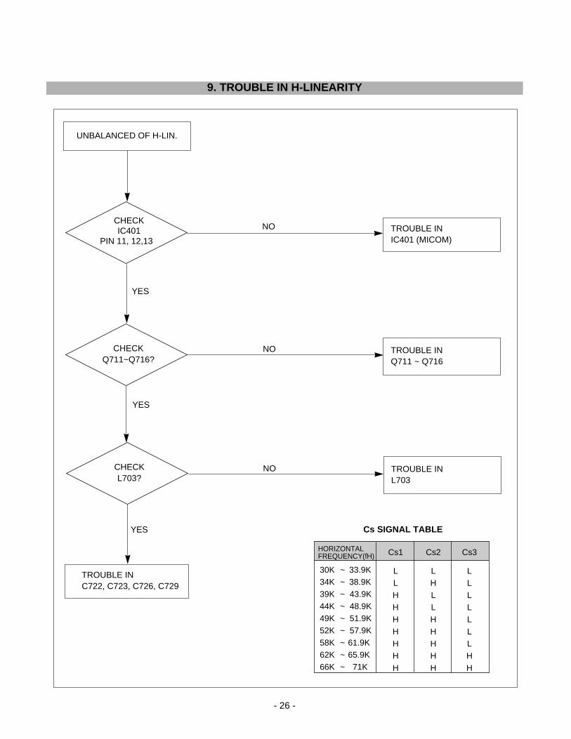
9. TROUBLE IN H-LINEARITY
UNBALANCED OF H-LIN.
CHECKIC401
PIN 11, 12,13
CHECK Q711~Q716?
CHECK L703?
TROUBLE IN IC401 (MICOM)
TROUBLE INQ711 ~ Q716
TROUBLE INL703
TROUBLE INC722, C723, C726, C729
NO
NO
NO
YES
YES
YES Cs SIGNAL TABLE
HORIZONTALFREQUENCY(fH)
30K ~ 33.9K34K ~ 38.9K39K ~ 43.9K44K ~ 48.9K49K ~ 51.9K52K ~ 57.9K58K ~ 61.9K62K ~ 65.9K66K ~ 71K
Cs1
LLHHHHHHH
Cs3
LLLLLLLHH
Cs2
LHLLHHHHH
Check if AC Voltage of IC401 Pin 35
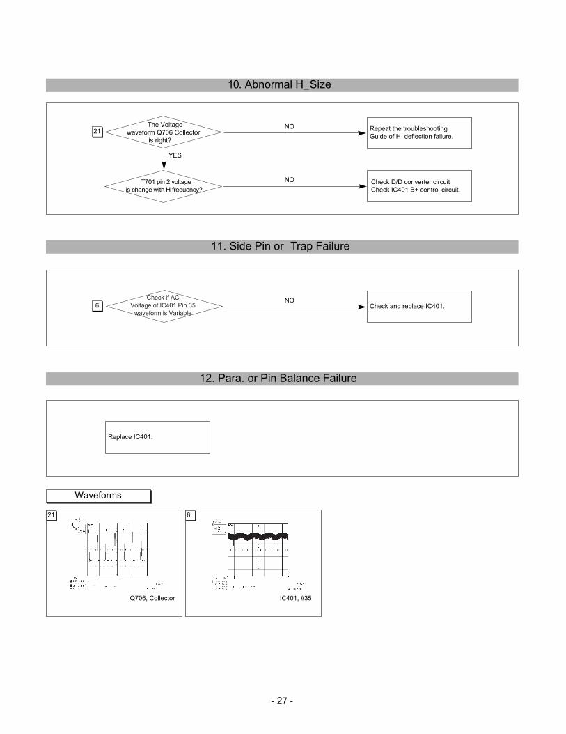
waveform is Variable
T701 pin 2 voltage is change with H frequency?
The Voltage waveform Q706 Collector
is right?
- 27 -
10. Abnormal H_Size
NO
NO
Repeat the troubleshootingGuide of H_deflection failure.
Check D/D converter circuitCheck IC401 B+ control circuit.
YES
11. Side Pin or Trap Failure
NO
12. Para. or Pin Balance Failure
Replace IC401.
Check and replace IC401.
Q706, Collector IC401, #35
21
6
21 6
Waveforms
8 9
98
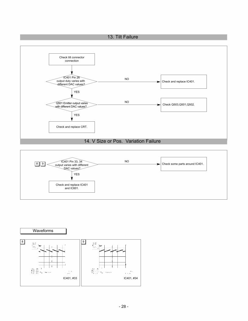
Q501 Emitter output varieswith different DAC values?
IC401 Pin 33, 34 output varies with different
DAC values?
IC401 Pin 26 output duty varies withdifferent DAC values?
13. Tilt Failure
Check tilt connector connection
Check and replace CRT.
NO
NO
Check and replace IC401.
Check Q503,Q501,Q502.
YES
YES
14. V Size or Pos. Variation Failure
Check and replace IC401 and IC601.
NOCheck some parts around IC401.
YES
- 28 -
IC401, #33 IC401, #34
Waveforms
Q706 collecter waveformis right?
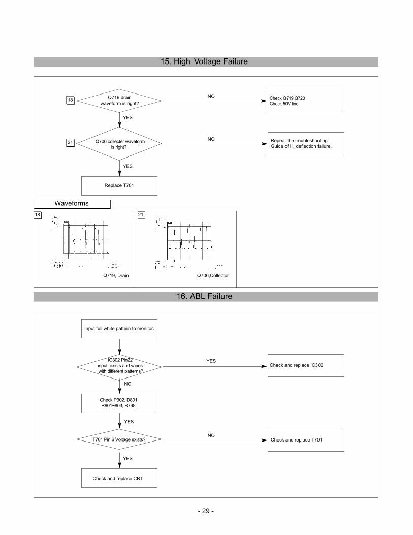
15. High Voltage Failure
NO
NO
Replace T701
Check Q719,Q720Check 50V line
Repeat the troubleshootingGuide of H_deflection failure.
YES
YES
16. ABL Failure
YES
NO
Check and replace CRT
Input full white pattern to monitor.
Check P302, D801, R801~803, R798.
Check and replace IC302
Check and replace T701
NO
YES
- 29 -
Q719, Drain Q706,Collector
IC302 Pin22 input exists and varieswith different patterns?
T701 Pin 6 Voltage exists?
18
18
Waveforms
21
21
YES
waveform is right? Q719 drain
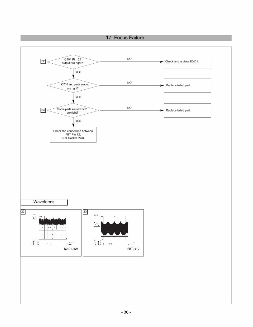
22 23
Some parts around T701are right?
IC401 Pin 24output are right?
Q710 and parts around are right?
17. Focus Failure
NO
NO
NO
Check the connection between FBT Pin 12,
CRT Socket PCB.
Check and replace IC401.
Waveforms
Replace failed part.
Replace failed part.
YES
YES
YES
- 30 -
IC401, #24 FBT, #12
22
23
3 4
43
IC401 Pin 23 input is High Active?
All in/output values areright?
IC401 Pin 45 and 46 inputs are right?
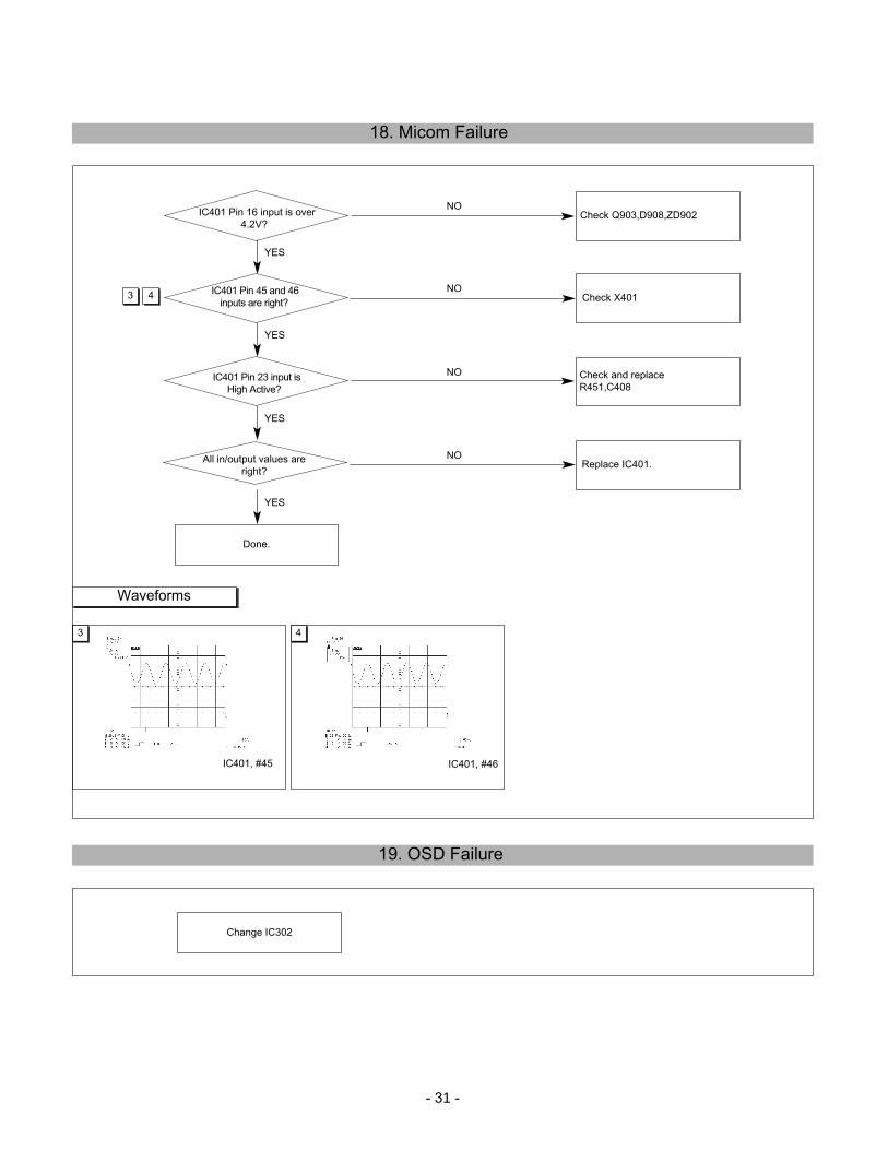
IC401 Pin 16 input is over4.2V?
18. Micom Failure
19. OSD Failure
NO
NO
NO
NO
Done.
Change IC302
Check Q903,D908,ZD902
Check X401
Check and replace R451,C408
Replace IC401.
YES
YES
YES
YES
- 31 -
IC401, #45 IC401, #46
Waveforms
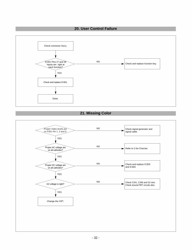
Proper Video levels areon P301 Pin 1, 3 and 5.
IC401 Pins 27 and 28inputs are right at
each function?
20. User Control Failure
Check connector Ass’y.
NO
Done.
Check and replace IC401.
Check and replace function key.
YES
21. Missing Color
NO
Change the CRT.
Check signal generator andsignal cable.
NORefer to 2 No Charcter.
NO Check and replace IC303and IC304
NO Check C341, C346 and G2 wire.Check around FBT circuits also.
YES
YES
YES
YES
- 32 -
Proper AC voltage areon all cathodes?
Proper DC voltage areon all cathodes?
G2 voltage is right?
Blank pedestal is on Pin 19, 20 and 21 of IC302
Is V_FLB and DC_bias onG1 Pin at CRT socket?
G2 voltage is right?
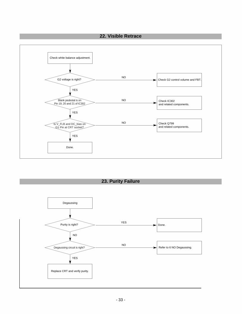
22. Visible Retrace
Check white balance adjustment.
NO
NO
NO
Done.
Check G2 control volume and FBT.
Check IC302and related components.
Check Q799 and related components.
YES
YES
YES
- 33 -
Degaussing circuit is right?
Purity is right?
23. Purity Failure
Degaussing
YES
NO
Replace CRT and verify purity.
Done.
Refer to 6 NO Degaussing.
NO
YES
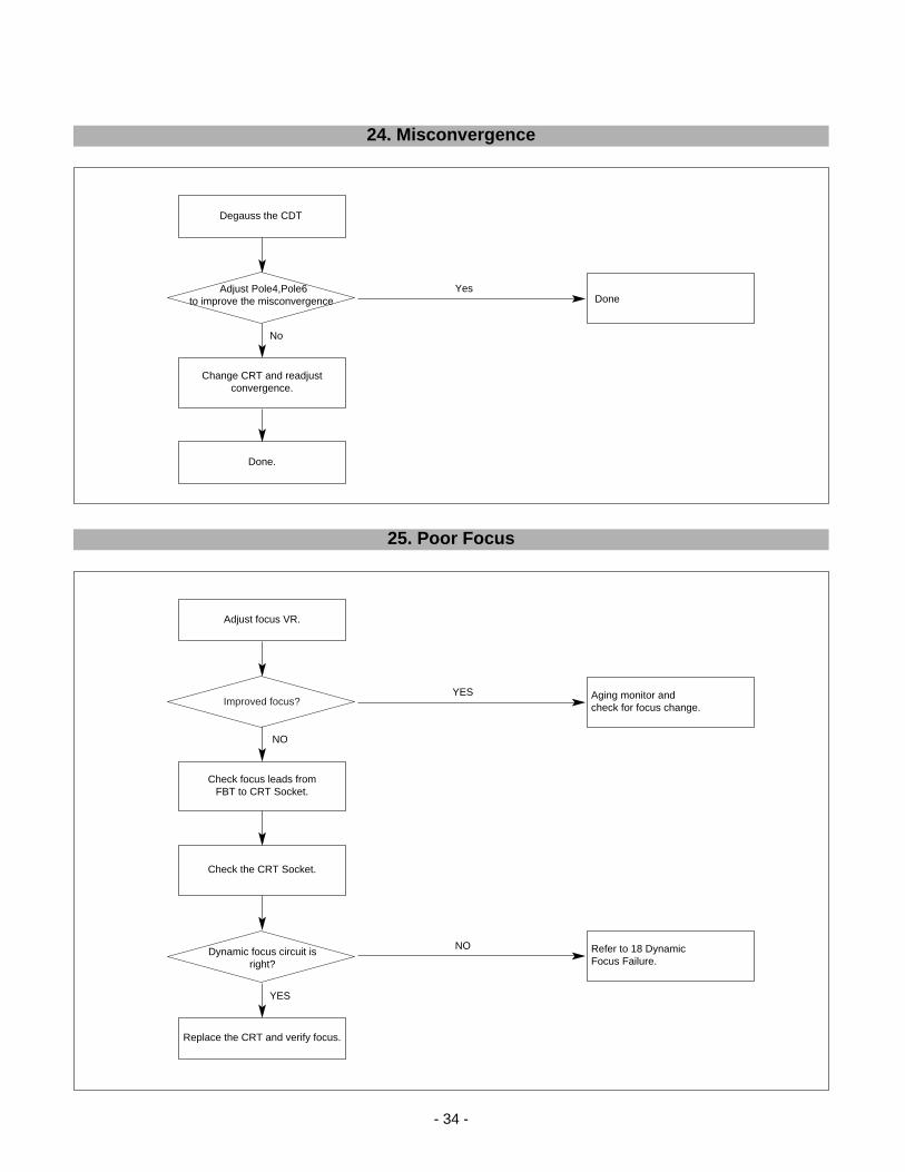
Improved focus?
Adjust Pole4,Pole6to improve the misconvergence
24. Misconvergence
Degauss the CDT
Done.
Change CRT and readjustconvergence.
YesDone
No
25. Poor Focus
Adjust focus VR.
Check focus leads fromFBT to CRT Socket.
Check the CRT Socket.
YES Aging monitor andcheck for focus change.
NO Refer to 18 DynamicFocus Failure.
NO
Replace the CRT and verify focus.
YES
- 34 -
Dynamic focus circuit isright?
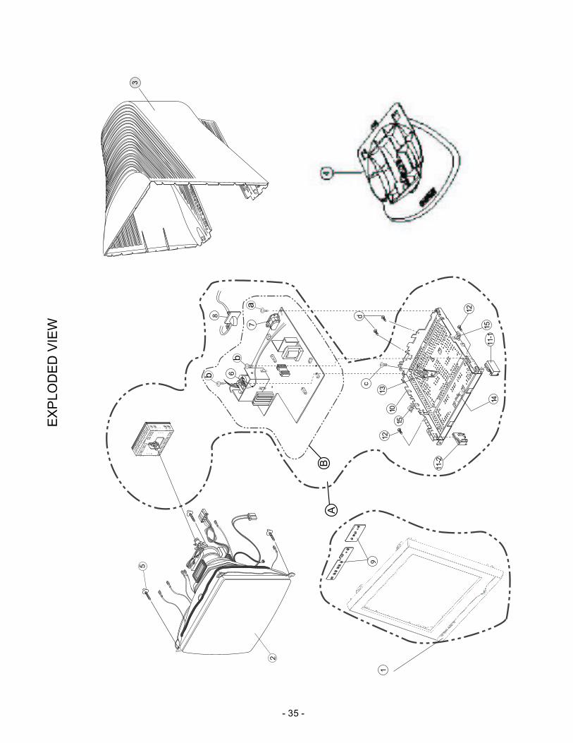
EX
PLO
DE
D V
IEW
- 35 -
1012
12
13
11-2
11-1
7
BA
2
6
5
a
b
b
1
d
1514
15
3
9c
8
EXPLODED VIEW PARTS LIST
- 36 -
Description
CDT(CIRC), M41QEE903X 00 NDDV LG-PHILIPS 85KHZ 29.1MM BARE PLUS
TILT SWIVEL ASSEMBLY, E710BH T066 B058 60HR 8C358 BRAND
SCREW ASSEMBLY, TAPTITE P TYPE D5.0 L25.0 MSWR/FZMY .
FBT (FLY BACK TRANSFORMER) 1063A,F700BK(71K) JUNGWOO 17''
SOCKET(CIRC),POWER, SA-4S-061P-LF HUA JIE AC UNIVERSAL 3PIN BLACK
SOCKET(CIRC),POWER, SA-4S HUA JIE AC UNIVERSAL 3PIN BLACK
CABLE,D-SUB, UL20276-9C(4.9MM) AT 1500MM GRAY(85964) T710BM GM
PWB(PCB) ASSEMBLY,SUB, T730BHL CONTROL TOTAL BRAND MOU4.0
METAL, SHIELD BOTTOM,T730
BRACKET, CN771C SUPPORTER BOT.(RIGHT)
BRACKET, CN771C SUPPORTER BOT.(LEFT)
SCREW, PTP+4*20BP(MSWR/FZMY)
BRACKET, T530 HOLDER FBT
MAIN TOTAL ASSEMBLY, T730SHKM KLEUMED BRAND CA-136
PWB(PCB) ASSEMBLY,MAIN, T730SHKM KLEUMED BRAND CA-136
SCREW,DRAWING, D3.5 L10.0 MSWR/FZMY +SW3.5+RW3.5
SCREW ASSEMBLY, TAPTITE P TYPE D3.0 L10.0 MSWR/FZMY SW3+RW10
SCREW,DRAWING, PZP+3*10(MSWR/FZMY)
Part No.
6318L17035A
3043TKK108A
339-002K
6174T11004F
6620TKB003B
6620TKB002B
6850TA9018A
6871TST586T
4950TKS331A
4810TKK150A
4810TKK151A
332-102F
4810TKK204K
3313T17004B
68719MT006B
332-112F
4001TKK004E
332-095B
Ref. No.
1
2
3
4
5
6
7
8
9
10
11-1
11-2
12
13
A
B
a
b
c
3809TKC050C BACK COVER ASSEMBLY, T710BH/PH C046 AF320T, 8C358(EQ54)
14
15
4930TKK036A
4930TKK031C
HOLDER,PCB FIX FB770G
HOLDER,PCB FIX,PC+ABS
d 332-110A SCREW, PZS+3*6(MSWR/FZMY)
3091TKC130R CABINET ASSEMBLY, T730SHL BRAND C097 SILVER B/VIEW MPRII MOU4.0
6318L17023D CDT(CIRC), M41QEE903X 21 QDDP LG-PHILIPS 85KHZ 29.1MM FCDT TCO PLUS
3091TKC145U CABINET ASSEMBLY, T730SHL BRAND C097 ABS MPRII B/VIEW SILVER SP
TILT SWIVEL ASSEMBLY, T730B T066 B060 FR-ABS 8C3583043900016B
CABLE,D-SUB, UL20276-9C(5.8MM) AT 1500MM BLACK 9930 700BJ DM6850TA9012C
PWB(PCB) ASSEMBLY,SUB, T730SHL CA-136 KLBRMES LGESP6871TST586Z
BRACKET, 700BK HOLDER FBT H-CKD4810TKK204J
MAIN TOTAL ASSEMBLY, T730SHM KLBRMES BRAND CA-1363313T17004F
PWB(PCB) ASSEMBLY,MAIN, T710BHM KLARMES BRAND CA-13668719MT006C
- 37-
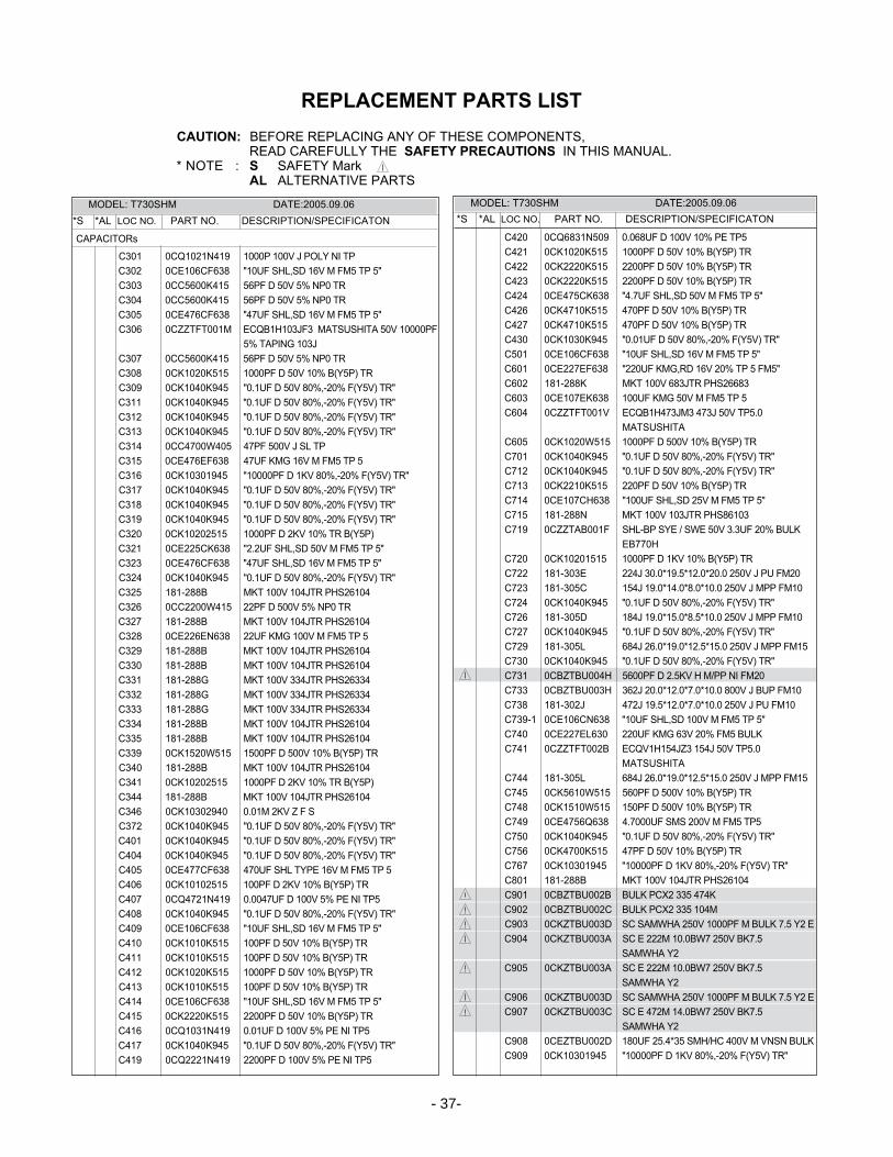
REPLACEMENT PARTS LISTCAUTION: BEFORE REPLACING ANY OF THESE COMPONENTS,
READ CAREFULLY THE SAFETY PRECAUTIONS IN THIS MANUAL.* NOTE : S SAFETY Mark
AL ALTERNATIVE PARTS
*S *AL LOC NO. PART NO. DESCRIPTION/SPECIFICATON
C A P A C I T O R s
C 3 0 1 0 C Q 1 0 2 1 N 4 1 9 1000P 100V J POLY NI TPC 3 0 2 0 C E 1 0 6 C F 6 3 8 "10UF SHL,SD 16V M FM5 TP 5"C 3 0 3 0 C C 5 6 0 0 K 4 1 5 56PF D 50V 5% NP0 TRC 3 0 4 0 C C 5 6 0 0 K 4 1 5 56PF D 50V 5% NP0 TRC 3 0 5 0 C E 4 7 6 C F 6 3 8 "47UF SHL,SD 16V M FM5 TP 5"C 3 0 6 0 C Z Z T F T 0 0 1 M ECQB1H103JF3 MATSUSHITA 50V 10000PF
5% TAPING 103JC 3 0 7 0 C C 5 6 0 0 K 4 1 5 56PF D 50V 5% NP0 TRC 3 0 8 0 C K 1 0 2 0 K 5 1 5 1000PF D 50V 10% B(Y5P) TRC 3 0 9 0 C K 1 0 4 0 K 9 4 5 "0.1UF D 50V 80%,-20% F(Y5V) TR"C 3 1 1 0 C K 1 0 4 0 K 9 4 5 "0.1UF D 50V 80%,-20% F(Y5V) TR"C 3 1 2 0 C K 1 0 4 0 K 9 4 5 "0.1UF D 50V 80%,-20% F(Y5V) TR"C 3 1 3 0 C K 1 0 4 0 K 9 4 5 "0.1UF D 50V 80%,-20% F(Y5V) TR"C 3 1 4 0 C C 4 7 0 0 W 4 0 5 47PF 500V J SL TPC 3 1 5 0 C E 4 7 6 E F 6 3 8 47UF KMG 16V M FM5 TP 5C 3 1 6 0 C K 1 0 3 0 1 9 4 5 "10000PF D 1KV 80%,-20% F(Y5V) TR"C 3 1 7 0 C K 1 0 4 0 K 9 4 5 "0.1UF D 50V 80%,-20% F(Y5V) TR"C 3 1 8 0 C K 1 0 4 0 K 9 4 5 "0.1UF D 50V 80%,-20% F(Y5V) TR"C 3 1 9 0 C K 1 0 4 0 K 9 4 5 "0.1UF D 50V 80%,-20% F(Y5V) TR"C 3 2 0 0 C K 1 0 2 0 2 5 1 5 1000PF D 2KV 10% TR B(Y5P)C 3 2 1 0 C E 2 2 5 C K 6 3 8 "2.2UF SHL,SD 50V M FM5 TP 5"C 3 2 3 0 C E 4 7 6 C F 6 3 8 "47UF SHL,SD 16V M FM5 TP 5"C 3 2 4 0 C K 1 0 4 0 K 9 4 5 "0.1UF D 50V 80%,-20% F(Y5V) TR"C 3 2 5 1 8 1 - 2 8 8 B MKT 100V 104JTR PHS26104C 3 2 6 0 C C 2 2 0 0 W 4 1 5 22PF D 500V 5% NP0 TRC 3 2 7 1 8 1 - 2 8 8 B MKT 100V 104JTR PHS26104C 3 2 8 0 C E 2 2 6 E N 6 3 8 22UF KMG 100V M FM5 TP 5C 3 2 9 1 8 1 - 2 8 8 B MKT 100V 104JTR PHS26104C 3 3 0 1 8 1 - 2 8 8 B MKT 100V 104JTR PHS26104C 3 3 1 1 8 1 - 2 8 8 G MKT 100V 334JTR PHS26334C 3 3 2 1 8 1 - 2 8 8 G MKT 100V 334JTR PHS26334C 3 3 3 1 8 1 - 2 8 8 G MKT 100V 334JTR PHS26334C 3 3 4 1 8 1 - 2 8 8 B MKT 100V 104JTR PHS26104C 3 3 5 1 8 1 - 2 8 8 B MKT 100V 104JTR PHS26104C 3 3 9 0 C K 1 5 2 0 W 5 1 5 1500PF D 500V 10% B(Y5P) TRC 3 4 0 1 8 1 - 2 8 8 B MKT 100V 104JTR PHS26104C 3 4 1 0 C K 1 0 2 0 2 5 1 5 1000PF D 2KV 10% TR B(Y5P)C 3 4 4 1 8 1 - 2 8 8 B MKT 100V 104JTR PHS26104C 3 4 6 0 C K 1 0 3 0 2 9 4 0 0.01M 2KV Z F SC 3 7 2 0 C K 1 0 4 0 K 9 4 5 "0.1UF D 50V 80%,-20% F(Y5V) TR"C 4 0 1 0 C K 1 0 4 0 K 9 4 5 "0.1UF D 50V 80%,-20% F(Y5V) TR"C 4 0 4 0 C K 1 0 4 0 K 9 4 5 "0.1UF D 50V 80%,-20% F(Y5V) TR"C 4 0 5 0 C E 4 7 7 C F 6 3 8 470UF SHL TYPE 16V M FM5 TP 5C 4 0 6 0 C K 1 0 1 0 2 5 1 5 100PF D 2KV 10% B(Y5P) TRC 4 0 7 0 C Q 4 7 2 1 N 4 1 9 0.0047UF D 100V 5% PE NI TP5C 4 0 8 0 C K 1 0 4 0 K 9 4 5 "0.1UF D 50V 80%,-20% F(Y5V) TR"C 4 0 9 0 C E 1 0 6 C F 6 3 8 "10UF SHL,SD 16V M FM5 TP 5"C 4 1 0 0 C K 1 0 1 0 K 5 1 5 100PF D 50V 10% B(Y5P) TRC 4 1 1 0 C K 1 0 1 0 K 5 1 5 100PF D 50V 10% B(Y5P) TRC 4 1 2 0 C K 1 0 2 0 K 5 1 5 1000PF D 50V 10% B(Y5P) TRC 4 1 3 0 C K 1 0 1 0 K 5 1 5 100PF D 50V 10% B(Y5P) TRC 4 1 4 0 C E 1 0 6 C F 6 3 8 "10UF SHL,SD 16V M FM5 TP 5"C 4 1 5 0 C K 2 2 2 0 K 5 1 5 2200PF D 50V 10% B(Y5P) TRC 4 1 6 0 C Q 1 0 3 1 N 4 1 9 0.01UF D 100V 5% PE NI TP5C 4 1 7 0 C K 1 0 4 0 K 9 4 5 "0.1UF D 50V 80%,-20% F(Y5V) TR"C 4 1 9 0 C Q 2 2 2 1 N 4 1 9 2200PF D 100V 5% PE NI TP5
C 4 2 0 0 C Q 6 8 3 1 N 5 0 9 0.068UF D 100V 10% PE TP5C 4 2 1 0 C K 1 0 2 0 K 5 1 5 1000PF D 50V 10% B(Y5P) TRC 4 2 2 0 C K 2 2 2 0 K 5 1 5 2200PF D 50V 10% B(Y5P) TRC 4 2 3 0 C K 2 2 2 0 K 5 1 5 2200PF D 50V 10% B(Y5P) TRC 4 2 4 0 C E 4 7 5 C K 6 3 8 "4.7UF SHL,SD 50V M FM5 TP 5"C 4 2 6 0 C K 4 7 1 0 K 5 1 5 470PF D 50V 10% B(Y5P) TRC 4 2 7 0 C K 4 7 1 0 K 5 1 5 470PF D 50V 10% B(Y5P) TRC 4 3 0 0 C K 1 0 3 0 K 9 4 5 "0.01UF D 50V 80%,-20% F(Y5V) TR"C 5 0 1 0 C E 1 0 6 C F 6 3 8 "10UF SHL,SD 16V M FM5 TP 5"C 6 0 1 0 C E 2 2 7 E F 6 3 8 "220UF KMG,RD 16V 20% TP 5 FM5"C 6 0 2 1 8 1 - 2 8 8 K MKT 100V 683JTR PHS26683C 6 0 3 0 C E 1 0 7 E K 6 3 8 100UF KMG 50V M FM5 TP 5C 6 0 4 0 C Z Z T F T 0 0 1 V ECQB1H473JM3 473J 50V TP5.0
M A T S U S H I T AC 6 0 5 0 C K 1 0 2 0 W 5 1 5 1000PF D 500V 10% B(Y5P) TRC 7 0 1 0 C K 1 0 4 0 K 9 4 5 "0.1UF D 50V 80%,-20% F(Y5V) TR"C 7 1 2 0 C K 1 0 4 0 K 9 4 5 "0.1UF D 50V 80%,-20% F(Y5V) TR"C 7 1 3 0 C K 2 2 1 0 K 5 1 5 220PF D 50V 10% B(Y5P) TRC 7 1 4 0 C E 1 0 7 C H 6 3 8 "100UF SHL,SD 25V M FM5 TP 5"C 7 1 5 1 8 1 - 2 8 8 N MKT 100V 103JTR PHS86103C 7 1 9 0 C Z Z T A B 0 0 1 F SHL-BP SYE / SWE 50V 3.3UF 20% BULK
E B 7 7 0 HC 7 2 0 0 C K 1 0 2 0 1 5 1 5 1000PF D 1KV 10% B(Y5P) TRC 7 2 2 1 8 1 - 3 0 3 E 224J 30.0*19.5*12.0*20.0 250V J PU FM20C 7 2 3 1 8 1 - 3 0 5 C 154J 19.0*14.0*8.0*10.0 250V J MPP FM10C 7 2 4 0 C K 1 0 4 0 K 9 4 5 "0.1UF D 50V 80%,-20% F(Y5V) TR"C 7 2 6 1 8 1 - 3 0 5 D 184J 19.0*15.0*8.5*10.0 250V J MPP FM10C 7 2 7 0 C K 1 0 4 0 K 9 4 5 "0.1UF D 50V 80%,-20% F(Y5V) TR"C 7 2 9 1 8 1 - 3 0 5 L 684J 26.0*19.0*12.5*15.0 250V J MPP FM15C 7 3 0 0 C K 1 0 4 0 K 9 4 5 "0.1UF D 50V 80%,-20% F(Y5V) TR"C 7 3 1 0 C B Z T B U 0 0 4 H 5600PF D 2.5KV H M/PP NI FM20C 7 3 3 0 C B Z T B U 0 0 3 H 362J 20.0*12.0*7.0*10.0 800V J BUP FM10C 7 3 8 1 8 1 - 3 0 2 J 472J 19.5*12.0*7.0*10.0 250V J PU FM10C 7 3 9 - 1 0 C E 1 0 6 C N 6 3 8 "10UF SHL,SD 100V M FM5 TP 5"C 7 4 0 0 C E 2 2 7 E L 6 3 0 220UF KMG 63V 20% FM5 BULKC 7 4 1 0 C Z Z T F T 0 0 2 B ECQV1H154JZ3 154J 50V TP5.0
M A T S U S H I T AC 7 4 4 1 8 1 - 3 0 5 L 684J 26.0*19.0*12.5*15.0 250V J MPP FM15C 7 4 5 0 C K 5 6 1 0 W 5 1 5 560PF D 500V 10% B(Y5P) TRC 7 4 8 0 C K 1 5 1 0 W 5 1 5 150PF D 500V 10% B(Y5P) TRC 7 4 9 0 C E 4 7 5 6 Q 6 3 8 4.7000UF SMS 200V M FM5 TP5C 7 5 0 0 C K 1 0 4 0 K 9 4 5 "0.1UF D 50V 80%,-20% F(Y5V) TR"C 7 5 6 0 C K 4 7 0 0 K 5 1 5 47PF D 50V 10% B(Y5P) TRC 7 6 7 0 C K 1 0 3 0 1 9 4 5 "10000PF D 1KV 80%,-20% F(Y5V) TR"C 8 0 1 1 8 1 - 2 8 8 B MKT 100V 104JTR PHS26104C 9 0 1 0 C B Z T B U 0 0 2 B BULK PCX2 335 474KC 9 0 2 0 C B Z T B U 0 0 2 C BULK PCX2 335 104MC 9 0 3 0 C K Z T B U 0 0 3 D SC SAMWHA 250V 1000PF M BULK 7.5 Y2 EC 9 0 4 0 C K Z T B U 0 0 3 A SC E 222M 10.0BW7 250V BK7.5
SAMWHA Y2C 9 0 5 0 C K Z T B U 0 0 3 A SC E 222M 10.0BW7 250V BK7.5
SAMWHA Y2C 9 0 6 0 C K Z T B U 0 0 3 D SC SAMWHA 250V 1000PF M BULK 7.5 Y2 EC 9 0 7 0 C K Z T B U 0 0 3 C SC E 472M 14.0BW7 250V BK7.5
SAMWHA Y2C 9 0 8 0 C E Z T B U 0 0 2 D 180UF 25.4*35 SMH/HC 400V M VNSN BULKC 9 0 9 0 C K 1 0 3 0 1 9 4 5 "10000PF D 1KV 80%,-20% F(Y5V) TR"
*S *AL LOC NO. PART NO. DESCRIPTION/SPECIFICATONMODEL: T730SHM DATE:2005.09.06 MODEL: T730SHM DATE:2005.09.06
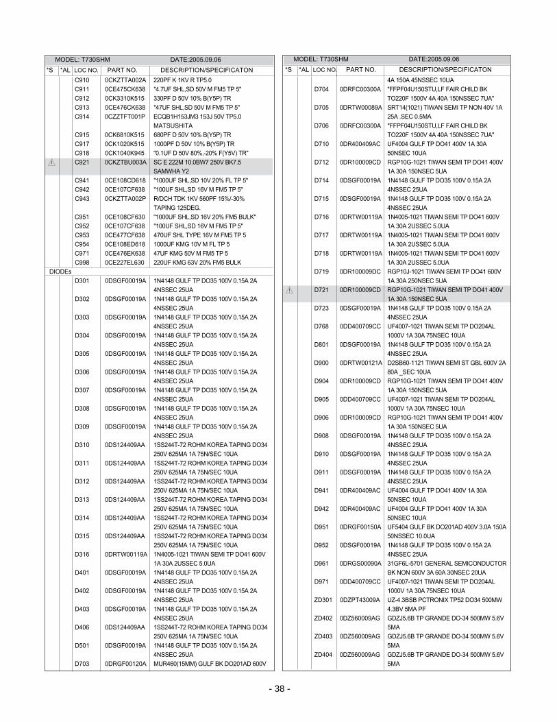
MODEL: T730SHM DATE:2005.09.06MODEL: T730SHM DATE:2005.09.06
C 9 1 0 0 C K Z T T A 0 0 2 A 220PF K 1KV R TP5.0C 9 1 1 0 C E 4 7 5 C K 6 3 8 "4.7UF SHL,SD 50V M FM5 TP 5"C 9 1 2 0 C K 3 3 1 0 K 5 1 5 330PF D 50V 10% B(Y5P) TRC 9 1 3 0 C E 4 7 6 C K 6 3 8 "47UF SHL,SD 50V M FM5 TP 5"C 9 1 4 0 C Z Z T F T 0 0 1 P ECQB1H153JM3 153J 50V TP5.0
M A T S U S H I T AC 9 1 5 0 C K 6 8 1 0 K 5 1 5 680PF D 50V 10% B(Y5P) TRC 9 1 7 0 C K 1 0 2 0 K 5 1 5 1000PF D 50V 10% B(Y5P) TRC 9 1 8 0 C K 1 0 4 0 K 9 4 5 "0.1UF D 50V 80%,-20% F(Y5V) TR"C 9 2 1 0 C K Z T B U 0 0 3 A SC E 222M 10.0BW7 250V BK7.5
SAMWHA Y2C 9 4 1 0 C E 1 0 8 C D 6 1 8 "1000UF SHL,SD 10V 20% FL TP 5"C 9 4 2 0 C E 1 0 7 C F 6 3 8 "100UF SHL,SD 16V M FM5 TP 5"C 9 4 3 0 C K Z T T A 0 0 2 P R/DCH TDK 1KV 560PF 15%/-30%
TAPING 125DEG.C 9 5 1 0 C E 1 0 8 C F 6 3 0 "1000UF SHL,SD 16V 20% FM5 BULK"C 9 5 2 0 C E 1 0 7 C F 6 3 8 "100UF SHL,SD 16V M FM5 TP 5"C 9 5 3 0 C E 4 7 7 C F 6 3 8 470UF SHL TYPE 16V M FM5 TP 5C 9 5 4 0 C E 1 0 8 E D 6 1 8 1000UF KMG 10V M FL TP 5C 9 7 1 0 C E 4 7 6 E K 6 3 8 47UF KMG 50V M FM5 TP 5C 9 9 8 0 C E 2 2 7 E L 6 3 0 220UF KMG 63V 20% FM5 BULK
D I O D E sD 3 0 1 0 D S G F 0 0 0 1 9 A 1N4148 GULF TP DO35 100V 0.15A 2A
4NSSEC 25UAD 3 0 2 0 D S G F 0 0 0 1 9 A 1N4148 GULF TP DO35 100V 0.15A 2A
4NSSEC 25UAD 3 0 3 0 D S G F 0 0 0 1 9 A 1N4148 GULF TP DO35 100V 0.15A 2A
4NSSEC 25UAD 3 0 4 0 D S G F 0 0 0 1 9 A 1N4148 GULF TP DO35 100V 0.15A 2A
4NSSEC 25UAD 3 0 5 0 D S G F 0 0 0 1 9 A 1N4148 GULF TP DO35 100V 0.15A 2A
4NSSEC 25UAD 3 0 6 0 D S G F 0 0 0 1 9 A 1N4148 GULF TP DO35 100V 0.15A 2A
4NSSEC 25UAD 3 0 7 0 D S G F 0 0 0 1 9 A 1N4148 GULF TP DO35 100V 0.15A 2A
4NSSEC 25UAD 3 0 8 0 D S G F 0 0 0 1 9 A 1N4148 GULF TP DO35 100V 0.15A 2A
4NSSEC 25UAD 3 0 9 0 D S G F 0 0 0 1 9 A 1N4148 GULF TP DO35 100V 0.15A 2A
4NSSEC 25UAD 3 1 0 0 D S 1 2 4 4 0 9 A A 1SS244T-72 ROHM KOREA TAPING DO34
250V 625MA 1A 75N/SEC 10UAD 3 1 1 0 D S 1 2 4 4 0 9 A A 1SS244T-72 ROHM KOREA TAPING DO34
250V 625MA 1A 75N/SEC 10UAD 3 1 2 0 D S 1 2 4 4 0 9 A A 1SS244T-72 ROHM KOREA TAPING DO34
250V 625MA 1A 75N/SEC 10UAD 3 1 3 0 D S 1 2 4 4 0 9 A A 1SS244T-72 ROHM KOREA TAPING DO34
250V 625MA 1A 75N/SEC 10UAD 3 1 4 0 D S 1 2 4 4 0 9 A A 1SS244T-72 ROHM KOREA TAPING DO34
250V 625MA 1A 75N/SEC 10UAD 3 1 5 0 D S 1 2 4 4 0 9 A A 1SS244T-72 ROHM KOREA TAPING DO34
250V 625MA 1A 75N/SEC 10UAD 3 1 6 0 D R T W 0 0 1 1 9 A 1N4005-1021 TIWAN SEMI TP DO41 600V
1A 30A 2USSEC 5.0UAD 4 0 1 0 D S G F 0 0 0 1 9 A 1N4148 GULF TP DO35 100V 0.15A 2A
4NSSEC 25UAD 4 0 2 0 D S G F 0 0 0 1 9 A 1N4148 GULF TP DO35 100V 0.15A 2A
4NSSEC 25UAD 4 0 3 0 D S G F 0 0 0 1 9 A 1N4148 GULF TP DO35 100V 0.15A 2A
4NSSEC 25UAD 4 0 6 0 D S 1 2 4 4 0 9 A A 1SS244T-72 ROHM KOREA TAPING DO34
250V 625MA 1A 75N/SEC 10UAD 5 0 1 0 D S G F 0 0 0 1 9 A 1N4148 GULF TP DO35 100V 0.15A 2A
4NSSEC 25UAD 7 0 3 0 D R G F 0 0 1 2 0 A MUR460(15MM) GULF BK DO201AD 600V
4A 150A 45NSSEC 10UAD 7 0 4 0 D R F C 0 0 3 0 0 A "FFPF04U150STU,LF FAIR CHILD BK
TO220F 1500V 4A 40A 150NSSEC 7UA"D 7 0 5 0 D R T W 0 0 0 8 9 A SRT14(1021) TIWAN SEMI TP NON 40V 1A
25A .SEC 0.5MAD 7 0 6 0 D R F C 0 0 3 0 0 A "FFPF04U150STU,LF FAIR CHILD BK
TO220F 1500V 4A 40A 150NSSEC 7UA"D 7 1 0 0 D R 4 0 0 4 0 9 A C UF4004 GULF TP DO41 400V 1A 30A
50NSEC 10UAD 7 1 2 0 D R 1 0 0 0 0 9 C D RGP10G-1021 TIWAN SEMI TP DO41 400V
1A 30A 150NSEC 5UAD 7 1 4 0 D S G F 0 0 0 1 9 A 1N4148 GULF TP DO35 100V 0.15A 2A
4NSSEC 25UAD 7 1 5 0 D S G F 0 0 0 1 9 A 1N4148 GULF TP DO35 100V 0.15A 2A
4NSSEC 25UAD 7 1 6 0 D R T W 0 0 1 1 9 A 1N4005-1021 TIWAN SEMI TP DO41 600V
1A 30A 2USSEC 5.0UAD 7 1 7 0 D R T W 0 0 1 1 9 A 1N4005-1021 TIWAN SEMI TP DO41 600V
1A 30A 2USSEC 5.0UAD 7 1 8 0 D R T W 0 0 1 1 9 A 1N4005-1021 TIWAN SEMI TP DO41 600V
1A 30A 2USSEC 5.0UAD 7 1 9 0 D R 1 0 0 0 0 9 D C RGP10J-1021 TIWAN SEMI TP DO41 600V
1A 30A 250NSEC 5UAD 7 2 1 0 D R 1 0 0 0 0 9 C D RGP10G-1021 TIWAN SEMI TP DO41 400V
1A 30A 150NSEC 5UAD 7 2 3 0 D S G F 0 0 0 1 9 A 1N4148 GULF TP DO35 100V 0.15A 2A
4NSSEC 25UAD 7 6 8 0 D D 4 0 0 7 0 9 C C UF4007-1021 TIWAN SEMI TP DO204AL
1000V 1A 30A 75NSEC 10UAD 8 0 1 0 D S G F 0 0 0 1 9 A 1N4148 GULF TP DO35 100V 0.15A 2A
4NSSEC 25UAD 9 0 0 0 D R T W 0 0 1 2 1 A D2SB60-1121 TIWAN SEMI ST GBL 600V 2A
80A _SEC 10UAD 9 0 4 0 D R 1 0 0 0 0 9 C D RGP10G-1021 TIWAN SEMI TP DO41 400V
1A 30A 150NSEC 5UAD 9 0 5 0 D D 4 0 0 7 0 9 C C UF4007-1021 TIWAN SEMI TP DO204AL
1000V 1A 30A 75NSEC 10UAD 9 0 6 0 D R 1 0 0 0 0 9 C D RGP10G-1021 TIWAN SEMI TP DO41 400V
1A 30A 150NSEC 5UAD 9 0 8 0 D S G F 0 0 0 1 9 A 1N4148 GULF TP DO35 100V 0.15A 2A
4NSSEC 25UAD 9 1 0 0 D S G F 0 0 0 1 9 A 1N4148 GULF TP DO35 100V 0.15A 2A
4NSSEC 25UAD 9 1 1 0 D S G F 0 0 0 1 9 A 1N4148 GULF TP DO35 100V 0.15A 2A
4NSSEC 25UAD 9 4 1 0 D R 4 0 0 4 0 9 A C UF4004 GULF TP DO41 400V 1A 30A
50NSEC 10UAD 9 4 2 0 D R 4 0 0 4 0 9 A C UF4004 GULF TP DO41 400V 1A 30A
50NSEC 10UAD 9 5 1 0 D R G F 0 0 1 5 0 A UF5404 GULF BK DO201AD 400V 3.0A 150A
50NSSEC 10.0UAD 9 5 2 0 D S G F 0 0 0 1 9 A 1N4148 GULF TP DO35 100V 0.15A 2A
4NSSEC 25UAD 9 6 1 0 D R G S 0 0 0 9 0 A 31GF6L-5701 GENERAL SEMICONDUCTOR
BK NON 600V 3A 60A 30NSEC 20UAD 9 7 1 0 D D 4 0 0 7 0 9 C C UF4007-1021 TIWAN SEMI TP DO204AL
1000V 1A 30A 75NSEC 10UAZ D 3 0 1 0 D Z P T 4 3 0 0 9 A UZ-4.3BSB PCTRONIX TP52 DO34 500MW
4.3BV 5MA PFZ D 4 0 2 0 D Z 5 6 0 0 0 9 A G GDZJ5.6B TP GRANDE DO-34 500MW 5.6V
5 M AZ D 4 0 3 0 D Z 5 6 0 0 0 9 A G GDZJ5.6B TP GRANDE DO-34 500MW 5.6V
5 M AZ D 4 0 4 0 D Z 5 6 0 0 0 9 A G GDZJ5.6B TP GRANDE DO-34 500MW 5.6V
5 M A
- 38 -
*S *AL LOC NO. PART NO. DESCRIPTION/SPECIFICATON*S *AL LOC NO. PART NO. DESCRIPTION/SPECIFICATON
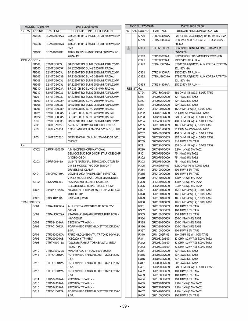
MODEL: T730SHM DATE:2005.09.06MODEL: T730SHM DATE:2005.09.06*S *AL LOC NO. PART NO. DESCRIPTION/SPECIFICATON
Z D 4 0 5 0 D Z 5 6 0 0 0 9 A G GDZJ5.6B TP GRANDE DO-34 500MW 5.6V 5 M A
Z D 4 0 6 0 D Z 5 6 0 0 0 9 A G GDZJ5.6B TP GRANDE DO-34 500MW 5.6V 5 M A
Z D 9 0 2 0 D Z 5 1 0 0 0 9 B E GDZ5.1B TP GRANDE DO34 500MW 5.1V 20MA .PF
C O I L s & C O R E sF B 3 0 2 6 2 1 0 T C E 0 0 3 L BAS3580T BO SUNG 3580MM AXIAL52MMF B 3 0 5 6 2 1 0 T C E 0 0 3 P BRS2550B BO SUNG 2550MM RADIALF B 3 0 6 6 2 1 0 T C E 0 0 3 L BAS3580T BO SUNG 3580MM AXIAL52MMF B 3 0 7 6 2 1 0 T C E 0 0 3 B BRS3580B BO SUNG 3580MM RADIALF B 3 0 8 6 2 1 0 T C E 0 0 3 J BAS2550T BO SUNG 2550MM AXIAL52MMF B 3 0 9 6 2 1 0 T C E 0 0 3 J BAS2550T BO SUNG 2550MM AXIAL52MMF B 3 1 0 6 2 1 0 T C E 0 0 3 A BRD3510B BO SUNG 3510MM RADIALF B 3 1 3 6 2 1 0 T C E 0 0 3 J BAS2550T BO SUNG 2550MM AXIAL52MMF B 7 0 1 6 2 1 0 T C E 0 0 3 L BAS3580T BO SUNG 3580MM AXIAL52MMF B 9 0 3 6 2 1 0 T C E 0 0 3 P BRS2550B BO SUNG 2550MM RADIALF B 9 0 5 6 2 1 0 T C E 0 0 3 J BAS2550T BO SUNG 2550MM AXIAL52MMF B 9 0 6 6 2 1 0 T C E 0 0 3 P BRS2550B BO SUNG 2550MM RADIALF B 9 2 1 6 2 1 0 T C E 0 0 3 A BRD3510B BO SUNG 3510MM RADIALF B 9 2 2 6 2 1 0 T C E 0 0 3 A BRD3510B BO SUNG 3510MM RADIALL 9 0 3 6 2 1 0 T C E 0 0 3 K BAS3550T BO SUNG 3550MM AXIAL52MML 7 0 2 6 1 4 0 T B Z 0 2 5 D "- - H-SIZE,DR12*20-C6.0,150UH 700BJ"L 7 0 3 6 1 4 0 T Y Z 0 1 3 A "LX31 SAMHWA DR14*15-C5.2,17.5T,5.6UH
T "L 7 0 5 6 1 4 0 T B Z 0 2 6 C DR15*18-C9.8 100UH 0.1*30MM 40.5T D/D
C H O K EI c s
I C 3 0 2 0 I P R P N S 0 2 5 D "LM1246DDE,NOPB NATIONAL SEMICONDUCTOR 24 DIP ST LF,ONE CHIP( V I D E O + O S D ) "
I C 3 0 3 0 I P R P 0 0 5 4 3 A LM2476 NATIONAL SEMICONDUCTOR T0-247 ST MONOLITHIC 3CH 6NS CRT DRIVE&BIAS CLAMP
I C 4 0 1 0 I M C R 0 2 1 1 9 A LGM41B-090A PHILIPS SDIP 56P STICK 71K L6 MIDDLE EAST OSD(LM1246/DDE)
I C 4 0 2 0 I S S 5 2 4 8 0 8 B "S524A60X81-DCB0,LF SAMSUNG ELECTRONICS 8DIP ST 8K EEPROM"
I C 6 0 1 0 I P R P P H 0 1 8 A "TDA4867J PHILIPS 9PIN,ST DIP VERTICALOUTPUT IC"
I C 9 0 1 0 I S S 3 8 4 2 0 0 A KA3842B (PWM)T R A N S I S T O R s
Q 5 0 1 0 T R A U 9 0 0 0 5 A AUK KOREA 2SC5342-Y TP TO92 32V 5 0 0 M A
Q 5 0 2 0 T R A U 8 0 0 2 9 A 2SA1979(A1270) AUK KOREA R/TP TO92 -40V -500MA
Q 5 0 3 0 T R 5 3 4 3 0 9 A A 2SC5343Y TP AUK - -Q 7 0 3 0 T F F C 1 0 0 1 2 A FQPF10N20C FAIRCHILD ST TO220F 200V
9 . 5 AQ 7 0 4 0 T R 3 9 0 4 0 9 C A FAIRCHILD 2N3904(TA) TP TO-92 60V 0.2AQ 7 0 5 0 T R 2 0 0 0 0 9 A B " K T C 2 0 0 - Y , T P , K E C "Q 7 0 6 0 T R T H 1 0 0 1 1 A "2SC5856(F,M),LF TOSHIBA ST 2-16E3A
1500V 14A"Q 7 1 0 0 T R K E 9 0 0 2 0 A MPSA44 KEC TP TO92 500V 300MAQ 7 1 1 0 T F F C 1 0 0 1 2 A FQPF10N20C FAIRCHILD ST TO220F 200V
9 . 5 AQ 7 1 2 0 T F F C 1 0 0 1 2 A FQPF10N20C FAIRCHILD ST TO220F 200V
9 . 5 AQ 7 1 3 0 T F F C 1 0 0 1 2 A FQPF10N20C FAIRCHILD ST TO220F 200V
9 . 5 AQ 7 1 4 0 T R 5 3 4 3 0 9 A A 2SC5343Y TP AUK - -Q 7 1 5 0 T R 5 3 4 3 0 9 A A 2SC5343Y TP AUK - -Q 7 1 6 0 T R 5 3 4 3 0 9 A A 2SC5343Y TP AUK - -Q 7 1 9 0 T F F C 1 0 0 1 2 A FQPF10N20C FAIRCHILD ST TO220F 200V
9 . 5 A
Q 7 2 0 0 T R 3 9 0 4 0 9 C A FAIRCHILD 2N3904(TA) TP TO-92 60V 0.2AQ 7 9 9 0 T R A U 8 0 0 3 6 A SPS92AT AUK KOREA R/TP TO92 -300V -
5 0 0 M AQ 9 0 1 0 T F F N 1 0 0 0 7 A SPA03N60C3 INFINEON ST TO-220FM
650V 3.2AQ 9 0 3 0 T R 1 0 0 8 0 9 A A KSC1008C-Y TP SAMSUNG TO92 NPNQ 9 4 1 0 T R 5 3 4 3 0 9 A A 2SC5343Y TP AUK - -Q 9 4 2 0 T R A U 8 0 0 3 4 A STB1277LAT(B1273) AUK KOREA R/TP TO-
92L -30V -2AQ 9 5 1 0 T R 5 3 4 3 0 9 A A 2SC5343Y TP AUK - -Q 9 5 2 0 T R A U 8 0 0 3 4 A STB1277LAT(B1273) AUK KOREA R/TP TO-
92L -30V -2AQ 9 5 3 0 T R 5 3 4 3 0 9 A A 2SC5343Y TP AUK - -
R E S I S T O R sD 7 2 4 0 R D 1 8 0 0 A 6 0 9 180 OHM 1/2 W(7.0) 5.00% TA52L 3 0 1 0 R D 0 8 2 2 Q 6 0 9 82 1/4W(3 5% TA52L 3 0 2 0 R D 0 8 2 2 Q 6 0 9 82 1/4W(3 5% TA52L 3 0 3 0 R D 0 8 2 2 Q 6 0 9 82 1/4W(3 5% TA52R 2 0 1 0 R D 1 0 0 1 Q 6 0 9 1K OHM 1/4 W(3.4) 5.00% TA52R 2 0 2 0 R D 0 9 1 2 Q 6 0 9 91 OHM 1/4 W (3.4) 5% TA52R 2 0 3 0 R D 2 2 0 0 Q 6 0 9 220 OHM 1/4 W(3.4) 5.00% TA52R 2 0 4 0 R D 4 3 0 0 Q 6 0 9 430 OHM 1/4 W(3.4) 5.00% TA52R 2 0 5 0 R D 1 0 0 1 Q 6 0 9 1K OHM 1/4 W(3.4) 5.00% TA52R 2 0 6 0 R D 0 9 1 2 Q 6 0 9 91 OHM 1/4 W (3.4) 5% TA52R 2 0 7 0 R D 4 3 0 0 Q 6 0 9 430 OHM 1/4 W(3.4) 5.00% TA52R 2 0 8 0 R D 2 2 0 0 Q 6 0 9 220 OHM 1/4 W(3.4) 5.00% TA52R 2 0 9 0 R D 9 1 0 0 Q 6 0 9 910 1/4W(3 5% TA52R 2 1 1 0 R D 2 2 0 0 Q 6 0 9 220 OHM 1/4 W(3.4) 5.00% TA52R 2 2 0 0 R D 3 9 0 1 Q 6 0 9 3.90K 1/4W(3 5% TA52R 3 0 1 0 R D 0 7 5 2 Q 6 0 9 75 1/4W(3 5% TA52R 3 0 2 0 R D 0 7 5 2 Q 6 0 9 75 1/4W(3 5% TA52R 3 0 3 0 R D 0 7 5 2 Q 6 0 9 75 1/4W(3 5% TA52R 3 0 5 0 R N 6 2 0 1 F 4 0 9 6.2K OHM 1/6 W 1.00% TA52R 3 1 4 0 R D 1 0 0 0 Q 6 0 9 100 1/4W(3 5% TA52R 3 1 5 0 R D 1 0 0 0 Q 6 0 9 100 1/4W(3 5% TA52R 3 1 9 0 R D 4 7 0 1 Q 6 0 9 4.70K 1/4W(3 5% TA52R 3 2 0 0 R D 4 7 0 1 Q 6 0 9 4.70K 1/4W(3 5% TA52R 3 2 6 0 R D 2 2 0 1 Q 6 0 9 2.20K 1/4W(3 5% TA52R 3 2 7 0 R D 1 0 0 1 Q 6 0 9 1K OHM 1/4 W(3.4) 5.00% TA52R 3 2 8 0 R D 1 0 0 1 Q 6 0 9 1K OHM 1/4 W(3.4) 5.00% TA52R 3 2 9 0 R D 1 0 0 1 Q 6 0 9 1K OHM 1/4 W(3.4) 5.00% TA52R 3 3 0 0 R D 1 0 0 1 Q 6 0 9 1K OHM 1/4 W(3.4) 5.00% TA52R 3 3 1 0 R D 1 8 0 0 Q 6 0 9 180 1/4W(3 5% TA52R 3 3 2 0 R D 1 8 0 0 Q 6 0 9 180 1/4W(3 5% TA52R 3 3 3 0 R D 1 3 0 0 Q 6 0 9 130 1/4W(3 5% TA52R 3 3 4 0 R D 3 3 0 3 Q 6 0 9 330K 1/4W(3 5% TA52R 3 3 5 0 R D 3 3 0 3 Q 6 0 9 330K 1/4W(3 5% TA52R 3 3 6 0 R D 3 3 0 3 Q 6 0 9 330K 1/4W(3 5% TA52R 3 3 7 0 R D 1 0 0 0 Q 6 0 9 100 1/4W(3 5% TA52R 3 4 0 0 R N 1 0 0 2 F 4 0 9 10K OHM 1/6 W 1.00% TA52R 3 4 1 0 R D 0 3 3 2 A 6 0 9 33 OHM 1/2 W(7.0) 5.00% TA52R 3 4 2 0 R D 0 3 3 2 A 6 0 9 33 OHM 1/2 W(7.0) 5.00% TA52R 3 4 3 0 R D 0 3 3 2 A 6 0 9 33 OHM 1/2 W(7.0) 5.00% TA52R 3 4 4 0 R D 0 3 3 2 Q 6 0 9 33 1/4W(3 5% TA52R 3 4 5 0 R D 0 3 3 2 Q 6 0 9 33 1/4W(3 5% TA52R 3 4 6 0 R D 0 3 3 2 Q 6 0 9 33 1/4W(3 5% TA52R 3 4 7 0 R D 0 2 0 2 Q 6 0 9 20 1/4W(3 5% TA52R 4 0 1 0 R D 2 2 0 0 Q 6 0 9 220 OHM 1/4 W(3.4) 5.00% TA52R 4 0 2 0 R D 1 0 0 0 Q 6 0 9 100 1/4W(3 5% TA52R 4 0 3 0 R D 1 0 0 0 Q 6 0 9 100 1/4W(3 5% TA52R 4 0 4 0 R D 1 0 0 0 Q 6 0 9 100 1/4W(3 5% TA52R 4 0 5 0 R D 2 2 0 1 Q 6 0 9 2.20K 1/4W(3 5% TA52R 4 0 6 0 R D 2 2 0 1 Q 6 0 9 2.20K 1/4W(3 5% TA52R 4 0 7 0 R D 4 7 0 1 Q 6 0 9 4.70K 1/4W(3 5% TA52R 4 0 8 0 R D 1 0 0 0 Q 6 0 9 100 1/4W(3 5% TA52
- 39 -
*S *AL LOC NO. PART NO. DESCRIPTION/SPECIFICATON
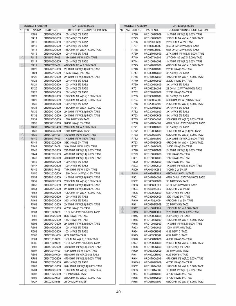
MODEL: T730SHM DATE:2005.09.06MODEL: T730SHM DATE:2005.09.06
R 4 0 9 0 R D 1 0 0 0 Q 6 0 9 100 1/4W(3 5% TA52R 4 1 1 0 R D 1 0 0 0 Q 6 0 9 100 1/4W(3 5% TA52R 4 1 2 0 R D 1 0 0 0 Q 6 0 9 100 1/4W(3 5% TA52R 4 1 3 0 R D 1 0 0 0 Q 6 0 9 100 1/4W(3 5% TA52R 4 1 4 0 R D 1 6 0 2 Q 6 0 9 16K OHM 1/4 W(3.4) 5.00% TA52R 4 1 5 0 R D 1 0 0 0 Q 6 0 9 100 1/4W(3 5% TA52R 4 1 6 0 R N 1 5 0 1 F 4 0 9 1.5K OHM 1/6 W 1.00% TA52R 4 1 7 0 R D 1 0 0 0 Q 6 0 9 100 1/4W(3 5% TA52R 4 1 9 0 R N 4 7 0 2 F 4 0 9 47K OHM 1/6 W 1.00% TA52R 4 2 0 0 R D 2 0 0 1 Q 6 0 9 2K OHM 1/4 W(3.4) 5.00% TA52R 4 2 1 0 R D 1 5 0 1 Q 6 0 9 1.50K 1/4W(3 5% TA52R 4 2 2 0 R D 2 0 0 1 Q 6 0 9 2K OHM 1/4 W(3.4) 5.00% TA52R 4 2 3 0 R D 1 0 0 0 Q 6 0 9 100 1/4W(3 5% TA52R 4 2 4 0 R D 1 0 0 0 Q 6 0 9 100 1/4W(3 5% TA52R 4 2 5 0 R D 1 0 0 0 Q 6 0 9 100 1/4W(3 5% TA52R 4 2 6 0 R D 1 0 0 0 Q 6 0 9 100 1/4W(3 5% TA52R 4 2 7 0 R D 1 0 0 2 Q 6 0 9 10K OHM 1/4 W(3.4) 5.00% TA52R 4 2 9 0 R D 1 0 0 2 Q 6 0 9 10K OHM 1/4 W(3.4) 5.00% TA52R 4 3 0 0 R D 1 0 0 0 Q 6 0 9 100 1/4W(3 5% TA52R 4 3 1 0 R D 1 8 0 2 Q 6 0 9 18K OHM 1/4 W(3.4) 5.00% TA52R 4 3 2 0 R D 2 0 0 1 Q 6 0 9 2K OHM 1/4 W(3.4) 5.00% TA52R 4 3 3 0 R D 2 0 0 1 Q 6 0 9 2K OHM 1/4 W(3.4) 5.00% TA52R 4 3 4 0 R D 1 5 0 3 Q 6 0 9 150K 1/4W(3 5% TA52R 4 3 6 0 R D 3 6 0 1 Q 6 0 9 3.60K 1/4W(3 5% TA52R 4 3 7 0 R N 2 7 0 2 G 4 0 9 27K OHM 1/4 W 1.00% TA52R 4 3 8 0 R D 1 3 0 3 Q 6 0 9 130K 1/4W(3 5% TA52R 4 3 9 0 R N 4 7 0 0 F 4 0 9 470 OHM 1/6 W 1.00% TA52R 4 4 0 0 R N 1 0 0 1 F 4 0 9 1K OHM 1/6 W 1.00% TA52R 4 4 1 0 R D 3 3 0 2 Q 6 0 9 33K 1/4W(3 5% TA52R 4 4 2 0 R N 3 9 0 1 F 4 0 9 3.9K OHM 1/6 W 1.00% TA52R 4 4 3 0 R D 2 2 0 0 Q 6 0 9 220 OHM 1/4 W(3.4) 5.00% TA52R 4 4 4 0 R D 4 7 0 0 Q 6 0 9 470 OHM 1/4 W(3.4) 5.00% TA52R 4 4 5 0 R D 4 7 0 0 Q 6 0 9 470 OHM 1/4 W(3.4) 5.00% TA52R 4 4 6 0 R D 1 0 0 0 Q 6 0 9 100 1/4W(3 5% TA52R 4 4 7 0 R D 1 0 0 0 Q 6 0 9 100 1/4W(3 5% TA52R 4 4 9 0 R N 7 5 0 1 F 4 0 9 7.5K OHM 1/6 W 1.00% TA52R 4 5 0 0 R D 1 2 0 3 Q 5 0 9 120K OHM 1/4 W (3.4) 2% TA52R 4 5 1 0 R D 1 0 0 1 Q 6 0 9 1K OHM 1/4 W(3.4) 5.00% TA52R 4 5 2 0 R D 2 0 0 2 Q 6 0 9 20K OHM 1/4 W(3.4) 5.00% TA52R 4 5 3 0 R D 2 0 0 1 Q 6 0 9 2K OHM 1/4 W(3.4) 5.00% TA52R 4 5 4 0 R D 2 0 0 1 Q 6 0 9 2K OHM 1/4 W(3.4) 5.00% TA52R 4 5 5 0 R D 1 0 0 2 Q 6 0 9 10K OHM 1/4 W(3.4) 5.00% TA52R 4 5 6 0 R D 1 0 0 0 Q 6 0 9 100 1/4W(3 5% TA52R 4 6 1 0 R D 3 9 0 0 Q 6 0 9 390 1/4W(3 5% TA52R 4 6 2 0 R D 2 0 0 1 Q 6 0 9 2K OHM 1/4 W(3.4) 5.00% TA52R 4 6 3 0 R D 4 7 0 1 Q 6 0 9 4.70K 1/4W(3 5% TA52R 5 0 1 0 R D 0 1 0 2 A 6 0 9 10 OHM 1/2 W(7.0) 5.00% TA52R 5 0 2 0 R D 8 2 0 2 Q 6 0 9 82K 1/4W(3 5% TA52R 5 0 3 0 R D 1 5 0 2 Q 6 0 9 15K 1/4W(3 5% TA52R 5 9 8 0 R D 2 0 0 1 Q 6 0 9 2K OHM 1/4 W(3.4) 5.00% TA52R 6 0 1 0 R D 1 0 0 0 Q 6 0 9 100 1/4W(3 5% TA52R 6 0 2 0 R D 1 0 0 0 Q 6 0 9 100 1/4W(3 5% TA52R 6 0 3 0 R N 0 2 2 0 H 6 0 9 0.22 1/2W 5% TA52R 6 0 4 0 R D 0 1 0 1 A 6 0 9 1 OHM 1/2 W(7.0) 5.00% TA52R 6 0 5 0 R D 0 1 0 2 A 6 0 9 10 OHM 1/2 W(7.0) 5.00% TA52R 6 0 6 0 R D 4 7 0 0 Q 6 0 9 470 OHM 1/4 W(3.4) 5.00% TA52R 6 0 7 0 R N 4 3 0 1 F 4 0 9 4.3K OHM 1/6 W 1.00% TA52R 6 0 8 0 R D 5 6 0 0 A 6 0 9 560 OHM 1/2 W(7.0) 0.05 TA52R 7 0 1 0 R D 4 7 0 0 Q 6 0 9 470 OHM 1/4 W(3.4) 5.00% TA52R 7 0 2 0 R D 6 2 0 0 Q 6 0 9 620 1/4W(3 5% TA52R 7 0 3 0 R D 5 6 0 1 Q 6 0 9 5.6K OHM 1/4 W(3.4) 5.00% TA52R 7 0 4 0 R D 1 0 0 2 Q 6 0 9 10K OHM 1/4 W(3.4) 5.00% TA52R 7 0 5 0 R D 0 1 0 2 Q 6 0 9 10 1/4W(3 5% TA52R 7 0 6 0 R D 3 3 0 2 A 6 0 9 33K OHM 1/2 W(7.0) 5.00% TA52R 7 2 7 0 R X 0 2 4 2 K 6 6 5 24 OHM 2 W 5% SF
R 7 2 8 0 R D 1 0 0 1 Q 6 0 9 1K OHM 1/4 W(3.4) 5.00% TA52R 7 2 9 0 R D 1 0 0 2 Q 6 0 9 10K OHM 1/4 W(3.4) 5.00% TA52R 7 3 6 0 R X 2 2 0 1 J 6 0 9 2.2KOHM 1 W 5% TA52R 7 3 7 0 R N 0 5 6 0 H 6 0 9 0.56 OHM 1/2 W 5.00% TA52R 7 3 8 0 R N 0 5 6 0 H 6 0 9 0.56 OHM 1/2 W 5.00% TA52R 7 3 9 0 R D 2 7 0 1 Q 6 0 9 2.7K OHM 1/4 W(3.4) 5.00% TA52R 7 4 0 0 R D 0 2 7 1 A 6 0 9 2.7 OHM 1/2 W(7.0) 5.00% TA52R 7 4 4 0 R D 1 0 0 1 A 6 0 9 1K OHM 1/2 W(7.0) 5.00% TA52R 7 4 5 0 R D 4 7 0 2 Q 6 0 9 47K OHM 1/4 W(3.4) 5.00% TA52R 7 4 6 0 R D 2 2 0 1 Q 6 0 9 2.20K 1/4W(3 5% TA52R 7 4 7 0 R D 3 0 0 1 Q 6 0 9 3K 1/4W(3 5% TA52R 7 4 8 0 R D 4 7 0 2 Q 6 0 9 47K OHM 1/4 W(3.4) 5.00% TA52R 7 4 9 0 R D 2 2 0 1 Q 6 0 9 2.20K 1/4W(3 5% TA52R 7 5 0 0 R D 3 0 0 1 Q 6 0 9 3K 1/4W(3 5% TA52R 7 5 1 0 R D 0 2 2 2 A 6 0 9 22 OHM 1/2 W(7.0) 5.00% TA52R 7 5 2 0 R D 2 2 0 1 Q 6 0 9 2.20K 1/4W(3 5% TA52R 7 5 3 0 R D 3 0 0 1 Q 6 0 9 3K 1/4W(3 5% TA52R 7 5 4 0 R D 6 8 0 0 A 6 0 9 680 OHM 1/2 W (7.0) 5% TA52R 7 5 6 0 R D 2 2 0 2 A 6 0 9 22K OHM 1/2 W(7.0) 5.00% TA52R 7 6 1 0 R D 3 0 0 1 Q 6 0 9 3K 1/4W(3 5% TA52R 7 6 2 0 R D 3 0 0 1 Q 6 0 9 3K 1/4W(3 5% TA52R 7 6 3 0 R D 3 0 0 1 Q 6 0 9 3K 1/4W(3 5% TA52R 7 6 5 0 R D 3 0 0 0 A 6 0 9 300 OHM 1/2 W(7.0) 5.00% TA52R 7 6 8 0 R D 4 7 0 3 A 6 0 9 470K OHM 1/2 W(7.0) 5.00% TA52R 7 7 1 0 R D 3 0 0 1 Q 6 0 9 3K 1/4W(3 5% TA52R 7 7 2 0 R D 1 2 0 2 Q 5 0 9 12K OHM 1/4 W (3.4) 2% TA52R 7 7 3 0 R D 6 2 0 2 A 6 0 9 62K OHM 1/2 W(7.0) 5.00% TA52R 7 8 2 0 R D 3 3 0 1 A 6 0 9 3.3K OHM 1/2 W(7.0) 5.00% TA52R 7 9 3 0 R D 4 7 0 2 Q 6 0 9 47K OHM 1/4 W(3.4) 5.00% TA52R 7 9 7 0 R D 1 5 0 1 Q 6 0 9 1.50K 1/4W(3 5% TA52R 7 9 8 0 R D 2 0 0 1 Q 6 0 9 2K OHM 1/4 W(3.4) 5.00% TA52R 7 9 9 0 R D 1 5 0 2 Q 6 0 9 15K 1/4W(3 5% TA52R 8 0 1 0 R D 1 5 0 2 Q 6 0 9 15K 1/4W(3 5% TA52R 8 0 2 0 R D 1 5 0 2 Q 6 0 9 15K 1/4W(3 5% TA52R 8 0 3 0 R D 1 0 0 1 Q 6 0 9 1K OHM 1/4 W(3.4) 5.00% TA52R 8 0 9 0 R X 0 1 0 1 K 6 6 5 1 OHM 2 W 5% SFR 8 1 8 0 R N 6 2 0 2 F 4 0 9 62KOHM 1/6 W 1% TA52R 9 0 1 0 R D 4 7 0 3 A 6 0 9 470K OHM 1/2 W(7.0) 5.00% TA52R 9 0 2 0 R D 0 3 3 2 Q 6 0 9 33 1/4W(3 5% TA52R 9 0 3 0 R D 0 5 6 2 F 6 0 9 56 OHM 1/6 W 5.00% TA52R 9 0 4 0 R X 3 9 0 2 K 6 6 5 39K OHM 2 W 5% SFR 9 0 6 0 R D 6 2 0 0 Q 6 0 9 620 1/4W(3 5% TA52R 9 0 7 0 R D 3 9 0 2 Q 6 0 9 39K 1/4W(3 5% TA52R 9 1 0 0 R X 4 7 0 2 J 6 0 9 47K OHM 1 W 5% TA52R 9 1 1 0 R D 0 2 0 2 Q 6 0 9 20 1/4W(3 5% TA52R 9 1 2 0 R N 1 8 0 2 F 4 0 9 18K OHM 1/6 W 1.00% TA52R 9 1 3 0 R N 2 7 0 1 F 4 0 9 2.7K OHM 1/6 W 1.00% TA52R 9 1 5 0 R D 2 0 0 0 Q 6 0 9 200 1/4W(3 5% TA52R 9 1 6 0 R D 1 0 0 2 Q 6 0 9 10K OHM 1/4 W(3.4) 5.00% TA52R 9 1 8 0 R D 1 0 0 1 Q 6 0 9 1K OHM 1/4 W(3.4) 5.00% TA52R 9 2 3 0 R D 1 0 0 3 Q 6 0 9 100K 1/4W(3 5% TA52R 9 2 4 0 R N 0 3 9 0 H 6 0 9 0.39 1/2W 5 TA52R 9 2 5 0 R N 0 3 9 0 H 6 0 9 0.39 1/2W 5 TA52R 9 2 6 0 R D 4 3 0 1 Q 6 0 9 4.30K 1/4W(3 5% TA52R 9 2 7 0 R D 2 0 0 2 Q 6 0 9 20K OHM 1/4 W(3.4) 5.00% TA52R 9 2 8 0 R D 1 8 0 0 Q 6 0 9 180 1/4W(3 5% TA52R 9 2 9 0 R D 0 3 3 2 Q 6 0 9 33 1/4W(3 5% TA52R 9 4 1 0 R N 0 2 2 0 H 6 0 9 0.22 1/2W 5% TA52R 9 4 4 0 R D 4 7 0 0 A 6 0 9 470 OHM 1/2 W(7.0) 5.00% TA52R 9 4 5 - 1 0 R D 4 7 0 1 Q 6 0 9 4.70K 1/4W(3 5% TA52R 9 5 2 0 R D 1 2 0 2 A 6 0 9 12K OHM 1/2 W(7.0) 5.00% TA52R 9 5 3 0 R D 1 0 0 1 A 6 0 9 1K OHM 1/2 W(7.0) 5.00% TA52R 9 5 4 0 R D 4 7 0 1 Q 6 0 9 4.70K 1/4W(3 5% TA52R 9 5 5 0 R D 4 7 0 1 Q 6 0 9 4.70K 1/4W(3 5% TA52R 9 5 6 0 R D 6 8 0 2 A 6 0 9 68K OHM 1/2 W(7.0) 5.00% TA52
- 40 -
*S *AL LOC NO. PART NO. DESCRIPTION/SPECIFICATON*S *AL LOC NO. PART NO. DESCRIPTION/SPECIFICATON
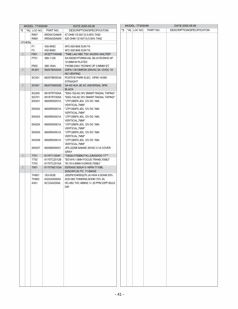
*S *AL LOC NO. PART NO. DESCRIPTION/SPECIFICATONR 9 5 7 0 R D 0 4 7 2 A 6 0 9 47 OHM 1/2 W(7.0) 5.00% TA52R 9 6 0 0 R D 6 2 0 0 A 6 0 9 620 OHM 1/2 W(7.0) 5.00% TA52
O T H E R sF 1 4 3 0 - 8 5 8 C AFC-520 BAE EUN TAF 2 4 3 0 - 8 5 8 C AFC-520 BAE EUN TAF 9 0 1 0 F Z Z T T H 0 0 4 B "TIME LAG HBC TSC 5A/250V,WALTER"P 7 0 1 3 6 6 - 1 1 2 K SA-0002K/YFW800-04L SE-A/YEONHO 4P
10.0MM NI PLATEDP 9 0 2 3 6 6 - 1 6 4 A YW396-03AV YEONHO 3P 3.96MM S/TR L 9 0 1 6 9 2 0 T B A 0 0 4 A G5PA-1-M OMRON 250VAC 5A 12VDC 1A
NO VENTINGS C 3 0 1 6 6 2 0 T B D 0 0 3 A PCS701E PARK ELEC. 10PIN 14/360
S T R A I G H TS C 9 0 1 6 6 2 0 T K B 0 0 2 B SA-4S HUA JIE AC UNIVERSAL 3PIN
B L A C KS G 3 0 5 6 9 1 8 T R T 0 0 5 A "SSG-102-A0,1KV SMART RADIAL TAPING"S G 7 0 1 6 9 1 8 T R T 0 0 5 A "SSG-102-A0,1KV SMART RADIAL TAPING"S W 2 0 1 6 6 0 0 R 0 0 0 0 1 A "JTP1280F6 JEIL 12V DC 1MA
V E R T I C A L , 7 M M "S W 2 0 2 6 6 0 0 R 0 0 0 0 1 A "JTP1280F6 JEIL 12V DC 1MA
V E R T I C A L , 7 M M "S W 2 0 3 6 6 0 0 R 0 0 0 0 1 A "JTP1280F6 JEIL 12V DC 1MA
V E R T I C A L , 7 M M "S W 2 0 4 6 6 0 0 R 0 0 0 0 1 A "JTP1280F6 JEIL 12V DC 1MA
V E R T I C A L , 7 M M "S W 2 0 5 6 6 0 0 R 0 0 0 0 1 A "JTP1280F6 JEIL 12V DC 1MA
V E R T I C A L , 7 M M "S W 2 0 6 6 6 0 0 R 0 0 0 0 1 A "JTP1280F6 JEIL 12V DC 1MA
V E R T I C A L , 7 M M "S W 2 0 7 6 6 0 0 M 0 0 0 0 5 1 JPS 2225B NAMAE 30VDC 0.1A COVER
G R A YT 7 0 1 6 1 7 4 T 1 1 0 0 4 F "1063A,F700BK(71K) JUNGWOO 17"""T 7 0 2 6 1 7 0 T C Z 0 1 2 B "EE1916 1.6MH FOCUS TRANS,700BJ"T 7 0 3 6 1 7 0 T C Z 0 1 5 A "EI-19 4.45MH H-DRIVE,700BJ"T 9 0 1 6 1 7 0 T M Z 1 5 3 A EER3435 300UH V-16PIN T710BL
SI/SC/NY/JS /TC 71-85KHZT H 9 0 1 1 6 3 - 0 5 3 E J502P61D4R5Q270 JA HWA 4.5OHM 20%T H 9 0 2 6 3 2 2 A 0 0 0 0 5 A SCK-083 THINKING 8OHM 15% 3AX 4 0 1 6 2 1 2 A A 2 0 0 4 L HC-49U TXC 48MHZ +/- 20 PPM 22PF BULK
D I P
- 41 -
*S *AL LOC NO. PART NO. DESCRIPTION/SPECIFICATONMODEL: T730SHM DATE:2005.09.06 MODEL: T730SHM DATE:2005.09.06
- 42 -- 43 -
SC
HE
MATIC
DIA
GR
AM
NO
TICE
Since this is a basic schem
atic diagram.
The value of components and som
e partial connection are sucject to be changed for im
provement w
ithout notice.
010123
0101
0126
0127
0128
0129
3031
0101
1401
1501
1601
1701
1801
1901
2001
2122
0102
0103
0104
0105
0106
0107
0108
0109
0110
Q901, D
rain
IC401, #20
IC601, #6
Q799, B
aseQ
799, Drain
Q719, D
rainQ
705,Drain
Q706,B
aseQ
706,Collector
Q704, G
ateIC
305, #5, 6, 7IC
302, #1IC
302, #24IC
302, #23IC
302, #19, 20, 21C
DT, R
K, G
K, B
K
IC901, #6
IC401, #45
IC401, #46
IC401, #18
IC401, #35
IC401, #33
IC401, #34
IC401, #52
01 11
IC401, #53
IC401, #21
IC401, #24
-45
-
DRA
OB
T IU
CRI
C DE
TNI
R P
) edi
S t
nen
op
mo
C( DR
AO
B NI
AM .
3)e
diS r
ed l
oS(
DRA
OB
NIA
M .4
)ed i
S t
nen
op
mo
C( DR
AO
B L
O RT
NO
C .1
)ed i
S re
dlo S
( DR
AO
B L
ORT
NO
C .2
-4
4 -

Sep 2005P/NO : 38289SL0019H Printed in China