Embed Size (px)
Citation preview
DESIGN TRADEOFF ANALYSIS
OF FLOATING-POINT
ADDER IN FPGAs
A Thesis Submitted to the College of
Graduate Studies and Research
In Partial Fulfillment of the Requirements
For the Degree of Master of Science
In the Department of Electrical Engineering
University of Saskatchewan
Saskatoon
By
Ali Malik
August 2005
© Copyright Ali Malik, August 2005. All rights reserved

i
PERMISSION TO USE
In presenting this thesis in partial fulfilment of the requirements for a Postgraduate Degree from the University of Saskatchewan, I agree that the Libraries of this University may make it freely available for inspection. I further agree that permission for copying of this thesis in any manner, in whole or in part, for scholarly purposes may be granted by the professor or professors who supervised my thesis work or, in their absence, by the Head of the Department or the Dean of the College in which my thesis work was done. It is understood that any copying or publication or use of this thesis or parts thereof for financial gain shall not be allowed without my written permission. It is also understood that due recognition shall be given to me and to the University of Saskatchewan in any scholarly use which may be made of any material in my thesis.
Requests for permission to copy or to make other use of material in this thesis in
whole or part should be addressed to: Head of the Department of Electrical Engineering University of Saskatchewan Saskatoon, Saskatchewan, S7N 5A9, Canada
ii
ABSTRACT
Field Programmable Gate Arrays (FPGA) are increasingly being used to design high-
end computationally intense microprocessors capable of handling both fixed and floating-
point mathematical operations. Addition is the most complex operation in a floating-point
unit and offers major delay while taking significant area. Over the years, the VLSI
community has developed many floating-point adder algorithms mainly aimed to reduce
the overall latency.
An efficient design of floating-point adder onto an FPGA offers major area and
performance overheads. With the recent advancement in FPGA architecture and area
density, latency has been the main focus of attention in order to improve performance.
Our research was oriented towards studying and implementing standard, Leading One
Predictor (LOP), and far and close data-path floating-point addition algorithms. Each
algorithm has complex sub-operations which lead significantly to overall latency of the
design. Each of the sub-operation is researched for different implementations and then
synthesized onto a Xilinx Virtex2p FPGA device to be chosen for best performance.
This thesis discusses in detail the best possible FPGA implementation for all the three
algorithms and will act as an important design resource. The performance criterion is
latency in all the cases. The algorithms are compared for overall latency, area, and levels
of logic and analyzed specifically for Virtex2p architecture, one of the latest FPGA
architectures provided by Xilinx. According to our results standard algorithm is the best
implementation with respect to area but has overall large latency of 27.059 ns while
occupying 541 slices. LOP algorithm improves latency by 6.5% on added expense of
38% area compared to standard algorithm. Far and close data-path implementation shows
iii
19% improvement in latency on added expense of 88% in area compared to standard
algorithm. The results clearly show that for area efficient design standard algorithm is the
best choice but for designs where latency is the criteria of performance far and close data-
path is the best alternative. The standard and LOP algorithms were pipelined into five
stages and compared with the Xilinx Intellectual Property [12]. The pipelined LOP gives
22% better clock speed on an added expense of 15% area when compared to Xilinx
Intellectual Property and thus a better choice for higher throughput applications. Test
benches were also developed to test these algorithms both in simulation and hardware.
Our work is an important design resource for development of floating-point adder
hardware on FPGAs. All sub components within the floating-point adder and known
algorithms are researched and implemented to provide versatility and flexibility to
designers as an alternative to intellectual property where they have no control over the
design. The VHDL code is open source and can be used by designers with proper
reference.

iv
ACKNOWLEDGEMENTS
First of all I would like to thank God for helping me at every step of my life. I would
like to express my gratitude to my supervisor, Professor Seok-Bum Ko, for his constant
support and guidance during the research work.
Also, I would like to thank the Department of Electrical Engineering and College of
Graduate Studies and Research, University of Saskatchewan, for providing graduate
scholarship during the course of my degree.
Finally, I wish to thank my father Iftikhar Ahmed, my mother Ruby Iftikhar, my
brother Omer and sister in law Nahdia for their endless support in my life and for helping
me get through my postgraduate studies.
v
TABLE OF CONTENTS
ABSTRACT........................................................................................................................ ii
ACKNOWLEDGEMENTS............................................................................................... iv
TABLE OF CONTENTS.................................................................................................... v
LIST OF FIGURES ......................................................................................................... viii
LIST OF TABLES............................................................................................................. ix
LIST OF ABBREVIATIONS............................................................................................. x
CHAPTER 1 INTRODUCTION ........................................................................................ 1
1.1 Motivation and Contribution..................................................................................... 2
1.2 Outline....................................................................................................................... 3
CHAPTER 2 BACKGROUND .......................................................................................... 4
2.1 Related Work............................................................................................................. 4
2.2 Xilinx Virtex2p FPGA Architecture ......................................................................... 7
CHAPTER 3 STANDARD FLOATING POINT REPRESENTATION AND ADDER
ALGORITHM..................................................................................................................... 9
3.1 Fixed Point and Floating Point Representations ....................................................... 9
3.1.1 Fixed-Point Representation ................................................................................ 9
3.1.2 2’s Complement Representation....................................................................... 10
3.1.3 Floating-Point Representation .......................................................................... 10
3.2 IEEE Floating Point Representation ....................................................................... 11
3.2.1 Basic Format..................................................................................................... 11
3.2.2 Rounding Modes............................................................................................... 14
3.2.3 Exceptions ........................................................................................................ 14
3.3 Standard Floating Point Addition Algorithm.......................................................... 15
3.3.1 Algorithm.......................................................................................................... 16
3.3.2 Micro-Architecture ........................................................................................... 17
3.3.3 Exponent Difference Module ........................................................................... 18
3.3.4 Right Shift Shifter............................................................................................. 20
3.3.5 2’s Complement Adder..................................................................................... 23
3.3.6 Leading One Detector....................................................................................... 24
vi
3.3.7 Left Shift Barrel Shifter.................................................................................... 28
3.3.8 Rounding .......................................................................................................... 29
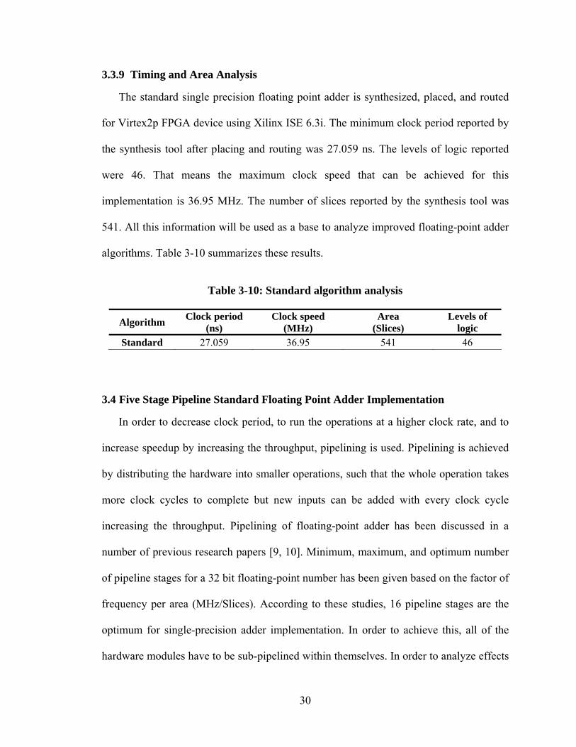
3.3.9 Timing and Area Analysis................................................................................ 30
3.4 Five Stage Pipeline Standard Floating Point Adder Implementation ..................... 30
3.4.1 Micro-Architecture ........................................................................................... 31
3.4.2 Timing and Area Comparison with Xilinx Intellectual Property ..................... 33
3.5 Conclusion............................................................................................................... 34
CHAPTER 4 IMPROVED FLOATING-POINT ADDER ALGORITHMS ................... 35
4.1 Leading One Predictor Algorithm........................................................................... 35
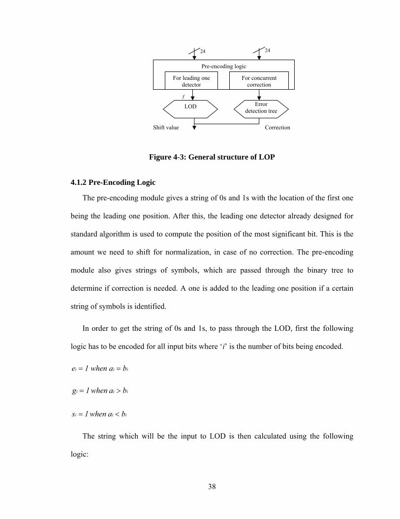
4.1.1 Leading One Predictor...................................................................................... 37
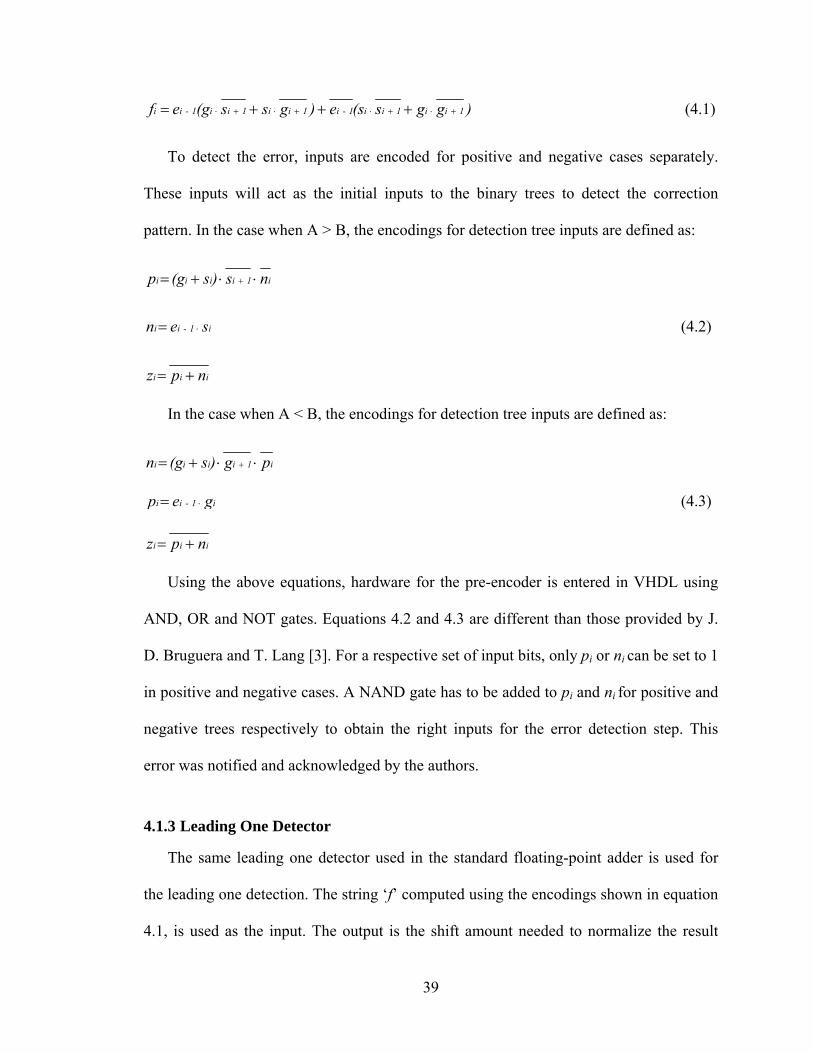
4.1.2 Pre-Encoding Logic.......................................................................................... 38
4.1.3 Leading One Detector....................................................................................... 39
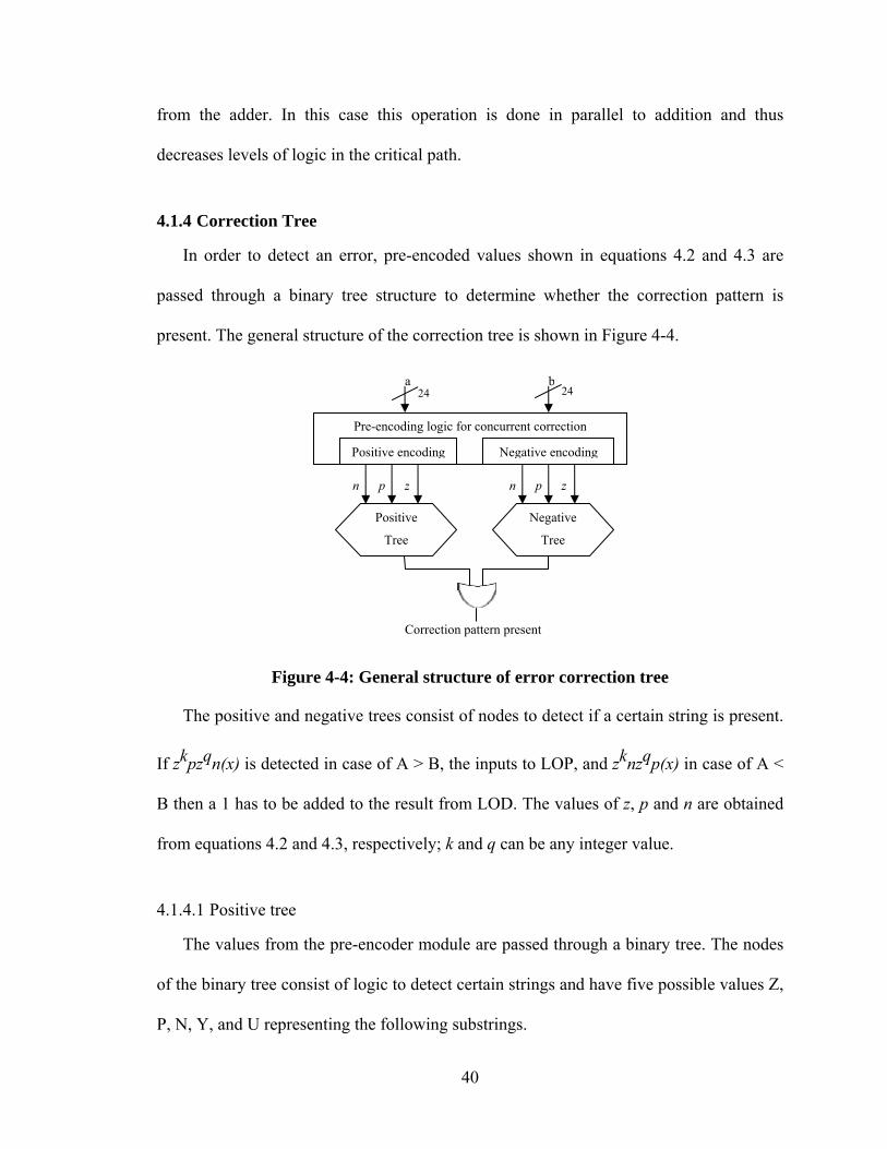
4.1.4 Correction Tree................................................................................................. 40
4.1.5 Timing and Area Analysis................................................................................ 43
4.2 Five Stage Pipeline LOP Floating Point Adder Implementation ............................ 44
4.2.1 Micro-Architecture ........................................................................................... 45
4.2.2 Timing and Area Comparison with Xilinx Intellectual Property ..................... 46
4.3 Far and Close Data-path Algorithm ........................................................................ 47
4.3.1 Algorithm.......................................................................................................... 47
4.3.2 Micro-Architecture ........................................................................................... 49
4.3.3 Close Path Micro-architecture .......................................................................... 49
4.3.4 Far Path Micro-architecture.............................................................................. 53
4.3.5 Sign Computation............................................................................................. 55
4.3.6 Timing and Area Analysis................................................................................ 56
4.4 Conclusion............................................................................................................... 58
CHAPTER 5 VERIFICATION AND VALIDATION..................................................... 59
5.1 Test Bench............................................................................................................... 59
5.2 Verification of Simulation....................................................................................... 61
5.3 Hardware Validation ............................................................................................... 62
CHAPTER 6 CONCLUSION........................................................................................... 63
6.1 Future Work ............................................................................................................ 65

vii
REFERENCES ................................................................................................................. 66
APPENDIX....................................................................................................................... 69
viii
LIST OF FIGURES
Figure 3-1: Binary representation and conversion to decimal of a numeric....................... 9
Figure 3-2: IEEE 754 single precision format .................................................................. 12
Figure 3-3: Flow chart for standard floating-point adder ................................................. 16
Figure 3-4: Micro-architecture of standard floating-point Adder..................................... 18
Figure 3-5: Hardware implementation for exponent difference ....................................... 19
Figure 3-6: Micro-architecture of barrel shifter................................................................ 21
Figure 3-7: Micro-architecture of align shifter ................................................................ 22
Figure 3-8: Hardware implementation for 2’s complement adder.................................... 23
Figure 3-9: Hardware implementation for LOD2............................................................. 25
Figure 3-10: Two level implementation of 4 bit LOD...................................................... 25
Figure 3-11: LOD4 logic implementation ........................................................................ 26
Figure 3-12: LOD implementation ................................................................................... 27
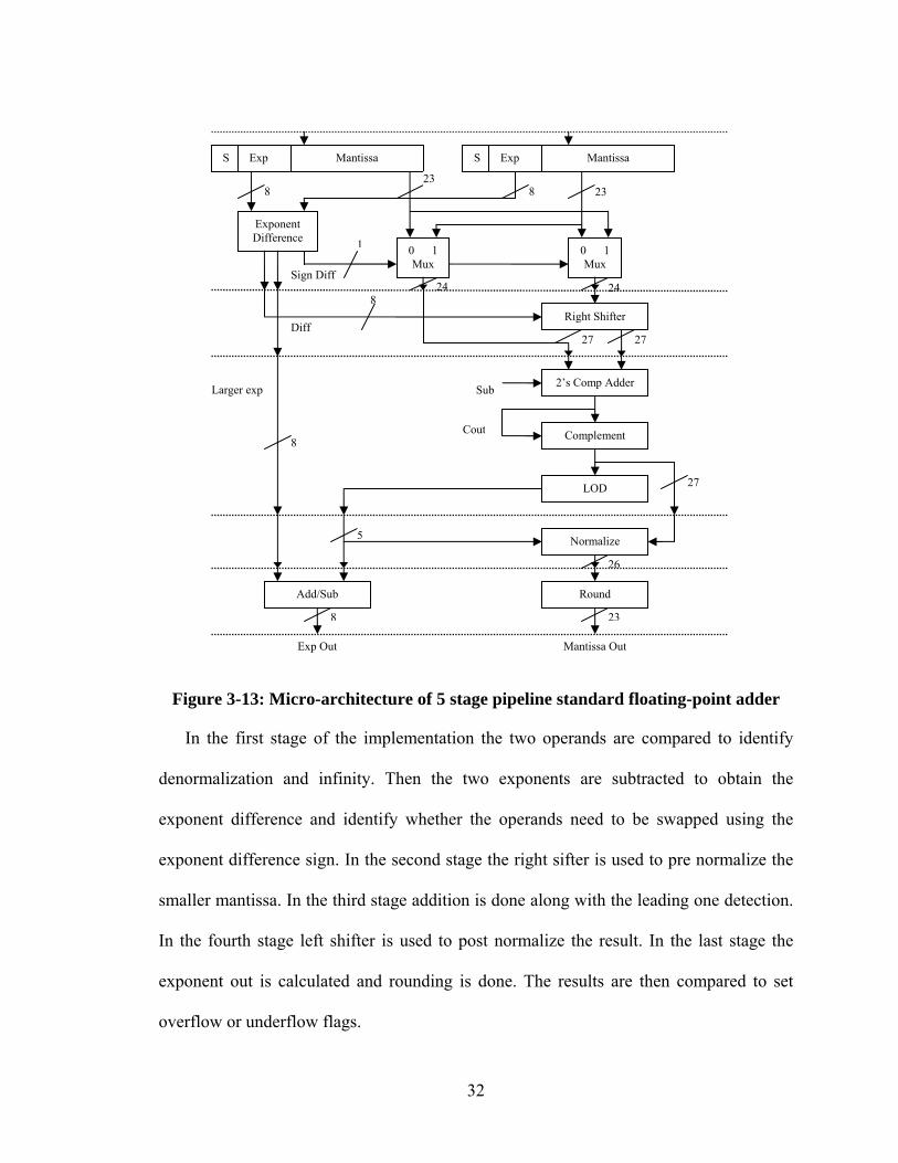
Figure 3-13: Micro-architecture of 5 stage pipeline standard floating-point adder.......... 32
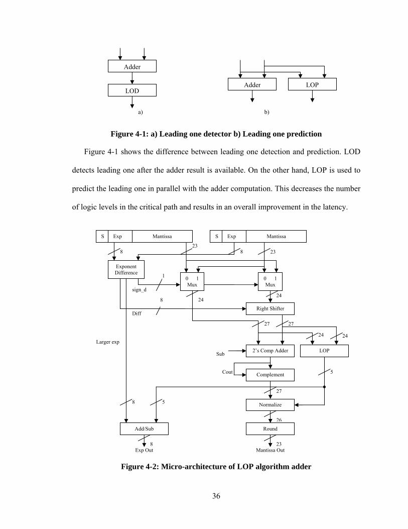
Figure 4-1: a) Leading one detector b) Leading one prediction ....................................... 36
Figure 4-2: Micro-architecture of LOP algorithm adder .................................................. 36
Figure 4-3: General structure of LOP ............................................................................... 38
Figure 4-4: General structure of error correction tree....................................................... 40
Figure 4-5: Binary tree to detect error detection pattern in z7pz8n(x) for positive pattern 42
Figure 4-6: Micro-architecture of 5 stage pipeline LOP floating-point adder.................. 45
Figure 4-7: Flow chart of far and close floating-point adder............................................ 48
Figure 4-8: Micro-architecture of far and close path floating-point adder ....................... 49
Figure 4-9: Micro-architecture of close path .................................................................... 50
Figure 4-10: Hardware implementation of compound adder............................................ 51
Figure 4-11: Micro-architecture of far path ...................................................................... 53
Figure 4-12: Latency and area comparison....................................................................... 57
Figure 5-1: Example Java test bench developer loop code............................................... 60
Figure 5-2: Example ModelSim run for floating-point adder........................................... 61
ix
LIST OF TABLES
Table 2-1: Logic resources of one CLB of Virtex 2p FPGA.............................................. 8
Table 3-1: Single and double precision format summary................................................. 12
Table 3-2: IEEE 754 single precision floating-point encoding ........................................ 13
Table 3-3: Adder implementation analysis ....................................................................... 20
Table 3-4: Shifter implementation analysis ...................................................................... 22
Table 3-5: Truth table for LOD2 ...................................................................................... 25
Table 3-6: Truth table for LOD4 with inputs from two LOD2’s...................................... 26
Table 3-7: Truth table for LOD8 with inputs from two LOD4’s...................................... 27
Table 3-8: LOD implementation analysis......................................................................... 28
Table 3-9: Left shifter implementation analysis ............................................................... 28
Table 3-10: Standard algorithm analysis .......................................................................... 30
Table 3-11: 5 stage pipeline standard implementation and Xilinx IP analysis................. 33
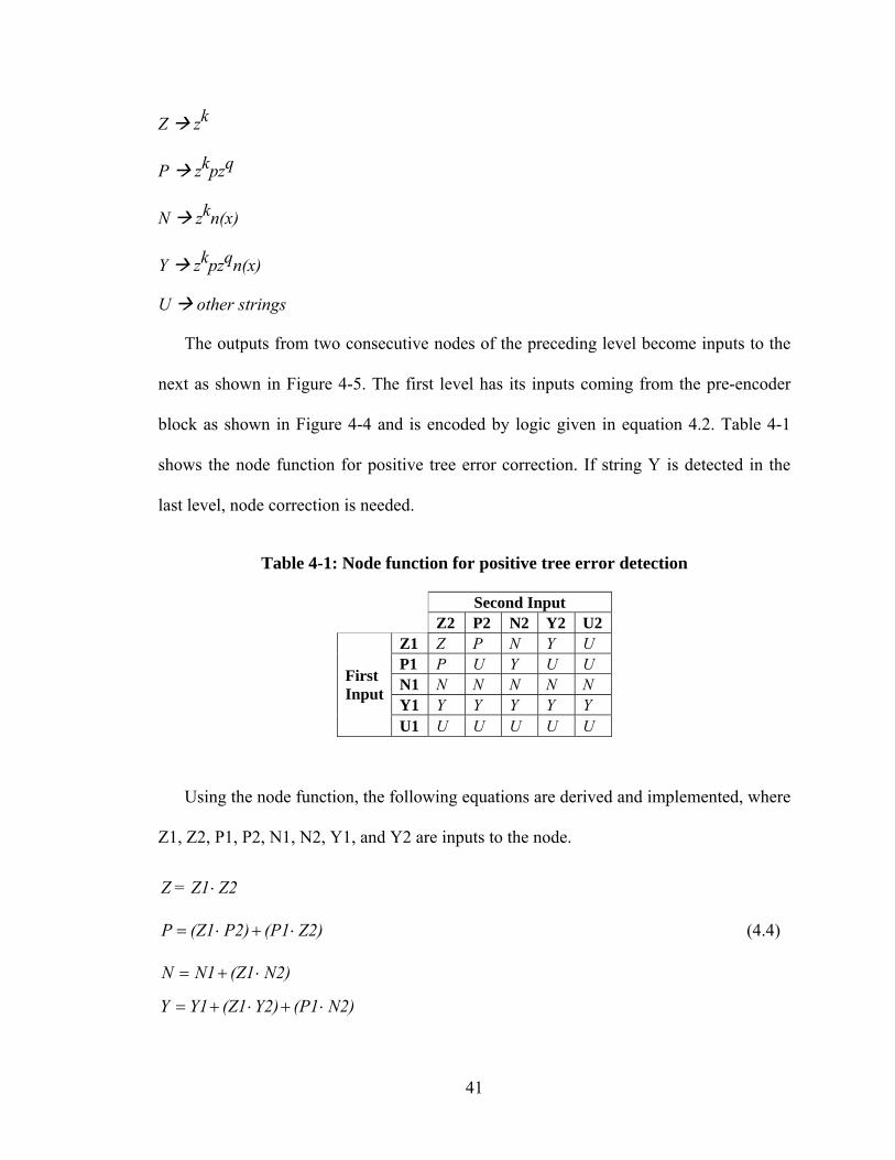
Table 4-1: Node function for positive tree error detection ............................................... 41
Table 4-2: Node function for negative tree error detection .............................................. 43
Table 4-3: Standard and LOP algorithm analysis ............................................................. 44
Table 4-4: 5 stage pipeline LOP implementation and Xilinx IP analysis......................... 46
Table 4-5: Standard and far and close data-path algorithm analysis ................................ 56
Table 4-6: LOP and far and close data-path algorithm analysis....................................... 56
x
LIST OF ABBREVIATIONS
ASIC Application Specific Integrated Circuit
CLB Configurable Logic Block
DSP Digital Signal Processing
FPGA Field Programmable Gate Arrays
IEEE Institute of Electrical and Electronics Engineers
IP Intellectual Property
ISE Integrated Software Environment
LOP Leading One Predictor
LOD Leading One Detector
LUT Look-Up Table
LZC Leading Zero Counter
NaN Not a Number
RAM Random Access Memory
REN Round towards Nearest Even
RP Round towards -∞
RM Round towards +∞
RZ Round towards 0
SOP Sum Of Product
VHSIC Very High Speed Integrated Circuit
VHDL VHSIC Hardware Description Language
VLSI Very Large Scale Integrated
1
CHAPTER 1 INTRODUCTION
Floating-point addition is the most frequent floating-point operation and accounts for
almost half of the scientific operation. Therefore, it is a fundamental component of math
coprocessor, DSP processors, embedded arithmetic processors, and data processing units.
These components demand high numerical stability and accuracy and hence are floating-
point based. Floating-point addition is a costly operation in terms of hardware and timing
as it needs different types of building blocks with variable latency. In floating-point
addition implementations, latency is the overall performance bottleneck. A lot of work
has been done to improve the overall latency of floating-point adders. Various algorithms
and design approaches have been developed by the Very Large Scale Integrated (VLSI)
circuit community [1-4] over the span of last two decades.
Field Programmable Gate Array (FPGA) is a silicon chip with unconnected logic
blocks, these logic blocks can be defined and redefined by user at anytime. FPGAs are
increasingly being used for applications which require high numerical stability and
accuracy. With less time to market and low cost, FPGAs are becoming a more attractive
solution compared to Application Specific Integrated Circuits (ASIC). FPGAs are mostly
used in low volume applications that cannot afford silicon fabrication or designs which
require frequent changes or upgrades. In FPGAs, the bottleneck for designing efficient
floating-point units has mostly been area. With advancement in FPGA architecture,
however, there is a significant increase in FPGA densities. Devices with millions of gates
2
and frequencies reaching up to 300 MHz are becoming more suitable for floating-point
arithmetic reliant applications.
1.1 Motivation and Contribution
For the most part, the digital design companies have resolved to FPGA design instead
of ASICs due to its effective time to market, adaptability and most importantly, its low
cost. Floating-point unit is one of the most important custom applications needed in most
hardware designs as it adds accuracy and ease of use. Floating-point adder is the most
complex operation in a floating-point unit and consists of many sub operations. A lot of
work has been done on floating-point adder and FPGAs which is summarized in chapter
2. However, to the best of our knowledge, there is no work which gives a detailed open
source analysis of different floating-point adder algorithms and different architectural
implementation of sub operations for floating-point adder on FPGA.
The main contribution and objective of our work is to implement and analyze
floating-point addition algorithms and hardware modules used to compute these
algorithms. These algorithms and modules are implemented using Very High Speed
Integrated Circuit (VHSIC) Hardware Description Language (VHDL), and then are
synthesized for Xilinx Virtex2p FPGA using Xilinx integrated software environment
(ISE) 6.3i [5]. Trade offs with respect to architectural level and algorithm level are
researched and explored. These implementations are placed and routed in the FPGA
device. Area and timing information for each design approach and algorithm is reported
and analyzed, thus giving designers more versatility in choosing the appropriate
algorithm in their design applications. VHDL code for each design approach is available
in the Appendix for reference.
3
1.2 Outline
This thesis is structured as follows. Chapter 2 gives the background information on
related work regarding implementation of FPGA and VLSI floating-point adder
algorithms and Virtex2p FPGA architecture. Chapter 3 provides an overview of IEEE
floating-point standard, and discusses hardware implementation and synthesis results of
standard floating-point adder algorithm. Chapter 4 describes the implementation and
synthesis results of improved floating-point adder algorithms including Leading One
Predictor (LOP) algorithm and far and close data-path adder algorithms. Chapter 5 goes
over the testing procedure, simulation, and hardware verification. Chapter 6 concludes
the thesis and provides recommendations for further research.
4
CHAPTER 2 BACKGROUND
Following the development in FPGA architectures and tools, many floating point
addition implementations are carried out on FPGAs. In this chapter, the related work
done in this area is overviewed. The architecture of our target FPGA device, Virtex2p by
Xilinx is also discussed briefly.
2.1 Related Work
One of the first competitive floating-point addition implementation is done by L.
Louca, T. Cook, and W. Johnson [6] in 1996. Single precision floating-point adder was
implemented for Altera FPGA device. The primary challenge was to fit the design in the
chip area while having reasonable timing convergence. The main objective of their
implementation was to achieve IEEE standard accuracy with reasonable performance
parameters. This is claimed to be the first IEEE single precision floating-point adder
implementation on a FPGA, before this, implementation with only 18-bit word length
was present [25].
Another research paper by W. Ligon, S. McMillan, G. Monn, F. Stivers, and K.
Underwood [7] discusses the use of reconfigurable hardware to perform high precision
operations on FPGAs which has been limited in the past by FPGA resources. The
practical implications of these operations in the Xilinx 4000 series FPGAs considering
densities available then and in the future are discussed. This paper is one of the first looks
at the future of computer arithmetic in terms of FPGA advancements.
5
Over time FPGA architecture and development tools evolved. One of the recent
papers related to FPGA architecture and floating-point units discussing novel
optimizations for arithmetic hardware was presented by E. Roesler, B. Nelson [8] in
2002. They discussed advancements in FPGA architecture, mainly high density fixed
circuit function blocks such as multiplier blocks and shift registers, and their effect on
floating-point unit operations including addition. They have shown that due to these
advancements in FPGA architecture significant area savings are achieved as compared to
old FPGA architectures.
The most important functionality of FPGA devices is their ability to reconfigure when
needed according to the design need. In 2003, J. Liang, R. Tessier and O. Mencer [9]
developed a tool which gives the user the option to create vast collection of floating-point
units with different throughput, latency, and area characteristics. Our work is related to
their work done but different in a way that we have taken each module inside the
floating-point adder and discussed its design tradeoffs, utilizing VLSI techniques. Their
result and analysis are directed more towards pipelining and the choice of optimization is
throughput. One of the drawbacks of their work is that they lack implementation of
overflow and underflow exceptions.
Latency is the overall bottleneck for any execution unit, and is defined as the time it
takes from reading the inputs to registering the outputs and exceptions for a single cycle
execution unit and is the basic criteria for performance. High clock speeds and
throughput can be achieved by adding numerous stages to the design and vary by design
needs. Latency is the fundamental performance criteria and thus choice of discussion and
6
comparison in our work. Our implementations also include overflow and underflow
exceptions.
One of the most recent works published related to our work is published by G.
Govindu, L. Zhuo, S. Choi, and V. Prasanna [10] on the analysis of high-performance
floating-point arithmetic on FPGAs. This paper has been an excellent resource for our
implementation and discussions throughout the research process, and provides possible
explanations. The results and analyses are based on number of pipeline stages as
parameter and throughput per area as the metric. All the implementations are done with
the latest Xilinx Virtex 2p FPGA device thus a good source for our work in evaluating
design techniques. The main difference between their work and our work is that they
have optimized the floating-point adder in terms of sub pipelining the sub components
thus increasing the throughput. On the other hand our work is concentrated on reducing
the latency of each sub component which is the key to overall latency. Another major
difference is that they have only discussed standard floating-point algorithm while in our
work standard, LOP, and far and close data-path algorithms are the parameter of
discussion.
Recently I have published a paper in 2005 [11] which discusses an effective
implementation of floating-point adder using the pipelined version of LOP later discussed
in Chapter 3 of this thesis. That design was customized in order to meet the design
criteria set by Xilinx Intellectual Property (IP) provided by Digital Core Design [12]. The
implementation shows significant improvement compared to the IP in terms of both clock
speed and area in some of the Xilinx FPGA architectures.
7
There are many commercial products related to floating-point adders [12, 13, 14]
which can be bought to be used in custom designs. Our work would be a great resource
for designers who want to custom design their product according to design needs as we
have described versatile implementations of different floating-point adder algorithms.
The VHDL code for all the implementations is given in the Appendix which can be
referred to while designing floating-point adders according to design resources and needs.
2.2 Xilinx Virtex2p FPGA Architecture
The variable-input Look-Up Table (LUT) architecture has been a fundamental
component of the Xilinx Virtex architecture first introduced in 1998 and now in its fourth
generation [5]. This distinctive architecture enables flexible implementation of any
function with eight variable inputs, as well as implementation of more complex functions.
In addition to being optimized for 4-, 5-, 6-, 7-, and 8- input LUT functions, the
architecture has been designed to support 32:1 multiplexers and Boolean functions with
up to 79 inputs. The Virtex architecture enables users to implement these functions with
minimal levels of logic. By collapsing levels of logic, users can achieve superior design
performance. The design is still based on the fundamental Configurable Logic Block
(CLB). According to Virtex2p datasheet [5], CLB resources include four slices and two
3-state buffers.
Each slice is equivalent and consists of two function generators (F & G), two storage
elements, arithmetic logic gates, large multiplexers, wide function capability, fast carry
look-ahead chain and horizontal cascade chain (OR gate). The function generators, F & G
are configurable as 4-input look-up tables (LUTs), as 16-bit shift registers, or as 16-bit
distributed Random Access Memory (RAM). In addition, the two storage elements are
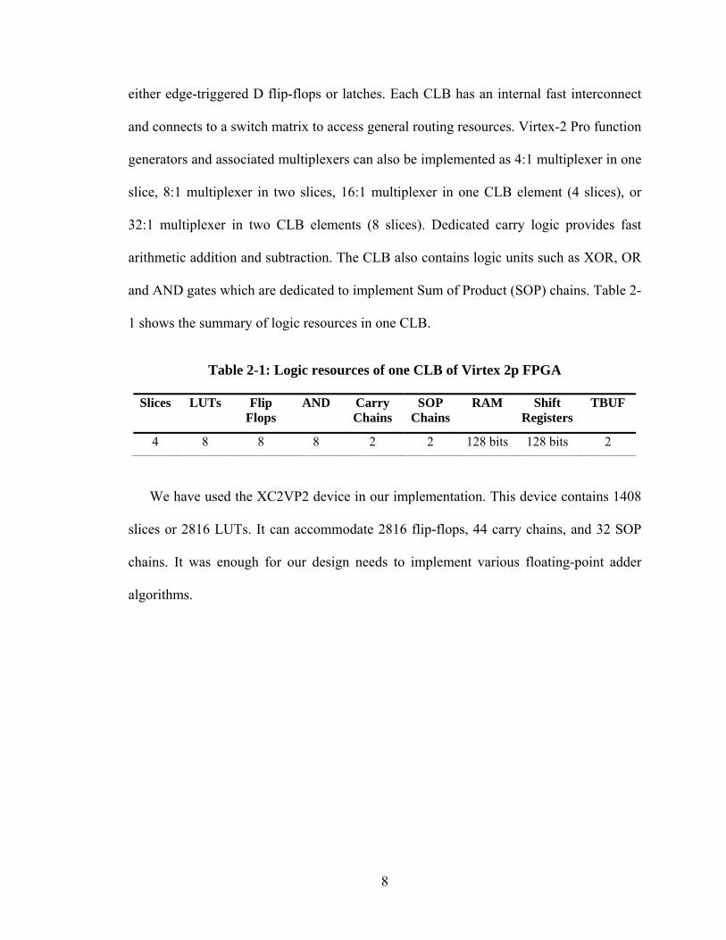
8
either edge-triggered D flip-flops or latches. Each CLB has an internal fast interconnect
and connects to a switch matrix to access general routing resources. Virtex-2 Pro function
generators and associated multiplexers can also be implemented as 4:1 multiplexer in one
slice, 8:1 multiplexer in two slices, 16:1 multiplexer in one CLB element (4 slices), or
32:1 multiplexer in two CLB elements (8 slices). Dedicated carry logic provides fast
arithmetic addition and subtraction. The CLB also contains logic units such as XOR, OR
and AND gates which are dedicated to implement Sum of Product (SOP) chains. Table 2-
1 shows the summary of logic resources in one CLB.
Table 2-1: Logic resources of one CLB of Virtex 2p FPGA
Slices LUTs Flip Flops
AND Carry Chains
SOP Chains
RAM Shift Registers
TBUF
4 8 8 8 2 2 128 bits 128 bits 2
We have used the XC2VP2 device in our implementation. This device contains 1408
slices or 2816 LUTs. It can accommodate 2816 flip-flops, 44 carry chains, and 32 SOP
chains. It was enough for our design needs to implement various floating-point adder
algorithms.
9
CHAPTER 3 STANDARD FLOATING POINT REPRESENTATION
AND ADDER ALGORITHM
This chapter gives a brief explanation on numerical encoding and the standard used to
represent floating-point arithmetic and the detail implementation of a prototype floating-
point adder.
3.1 Fixed Point and Floating Point Representations
Every real number has an integer part and a fraction part; a radix point is used to
differentiate between them. The number of binary digits assigned to the integer part may
be different to the number of digits assigned to the fractional part. A generic binary
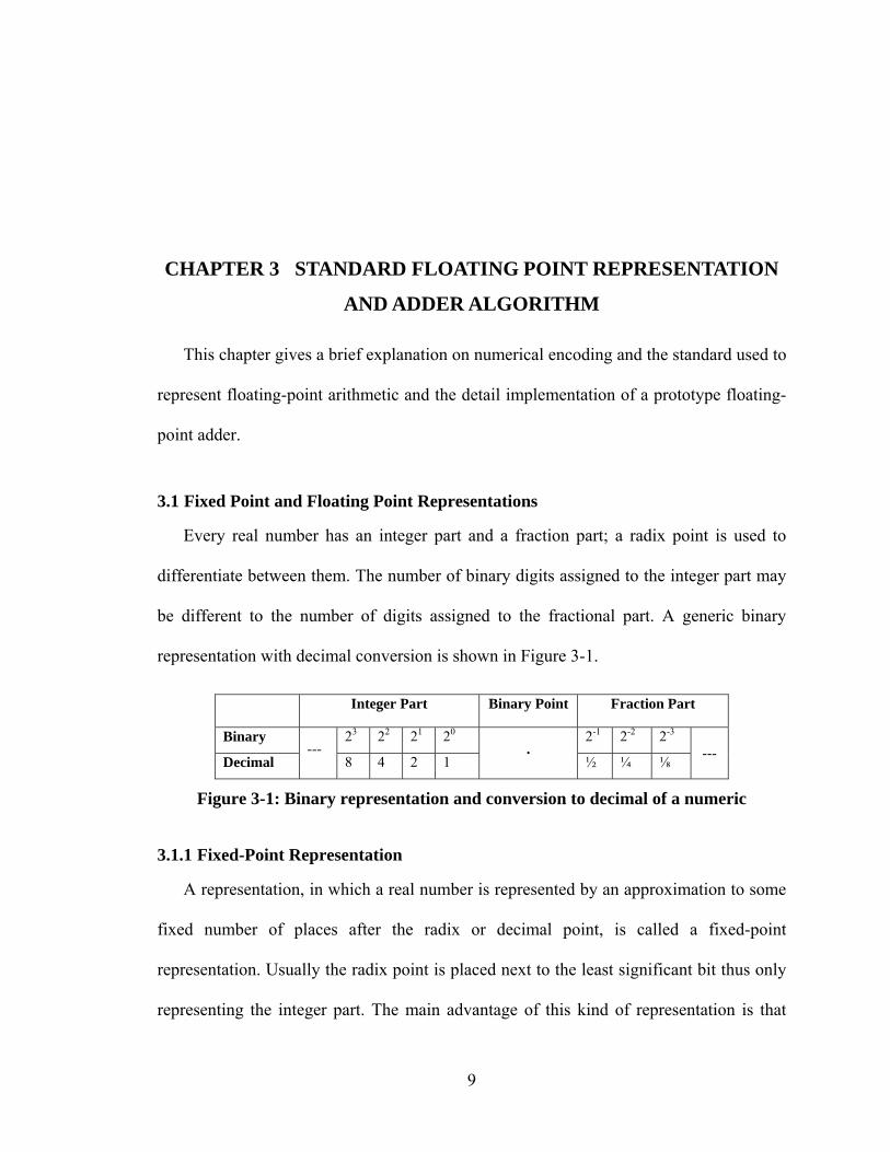
representation with decimal conversion is shown in Figure 3-1.
Integer Part Binary Point Fraction Part
Binary 23 22 21 20 2-1 2-2 2-3
Decimal ---
8 4 2 1 .
½ ¼ ⅛ ---
Figure 3-1: Binary representation and conversion to decimal of a numeric
3.1.1 Fixed-Point Representation
A representation, in which a real number is represented by an approximation to some
fixed number of places after the radix or decimal point, is called a fixed-point
representation. Usually the radix point is placed next to the least significant bit thus only
representing the integer part. The main advantage of this kind of representation is that
10
integer arithmetic can be applied to them and they can be stored using small values. This
helps making the operations faster and area efficient. The main disadvantage is that a
fixed-point number has limited or no flexibility, i.e., number of significant bits to the
right of the decimal point. Some of the other disadvantages are that the arithmetic
operations based on this representation can go into overflow and underflow often. The
fixed-point number also has a limited integer range and it is hard to represent very small
and big number in the same representation. These are some of the reasons why floating-
point representation and arithmetic was evolved to take care of these disadvantages.
3.1.2 2’s Complement Representation
In order to represent both positive and negative fixed-point numbers, 2’s complement
representation is used. Positive 2’s complement numbers are represented as simple
binary. Negative number is represented in a way that when it is added to a positive
number of same magnitudes the answer is zero. In 2’s complement representation, the
most significant bit is called the sign bit. If the sign bit is 0, the number is non-negative
,i.e., 0 or greater. If the sign bit is 1, the number is negative or less than 0. In order to
calculate a 2’s complement or a negative of a certain binary integer number, first 1’s
complement, i.e., bit inversion is done and then a 1 is added to the result.
3.1.3 Floating-Point Representation
In general, a floating-point number will be represented as ± d.dd... d × ßE, where
d.dd... d is called the significand and has p digits also called the precision of the number,
and ß is the base being 10 for decimal, 2 for binary or 16 for hexadecimal. If ß= 10 and p
= 3, then the number 0.1 is represented as 1.00 × 10⁻¹. If ß= 2 and p = 24, then the
11
decimal number 0.1 cannot be represented exactly, but is approximately
1.10011001100110011001101 × 2-4. This shows a number which is exactly represented
in one format lies between two floating-point numbers in another format. Thus the most
important factor of floating-point representation is the precision or number of bits used to
represent the significands. Other important parameters are Emax and Emin, the largest and
the smallest encoded exponents for a certain representation, giving the range of a number.
3.2 IEEE Floating Point Representation
The Institute of Electrical and Electronics Engineering (IEEE) issued 754 standard for
binary floating-point arithmetic in 1985 [15]. This standardization was needed to
eliminate computing industry’s arithmetic vagaries. Due to different definitions used by
different vendors, machine specific constraints were imposed on programmers and
clients. The standard specifies basic and extended floating-point number formats,
arithmetic operations, conversions between various number formats, and floating-point
exceptions. This section goes over the aspects of the standard used in implementing and
evaluating various floating-point adder algorithms.
3.2.1 Basic Format
There are two basic formats described in IEEE 754 format, double-precision using
64-bits and single-precision using 32-bits. Table 3-1 shows the comparison between the
important aspects of the two representations.
12
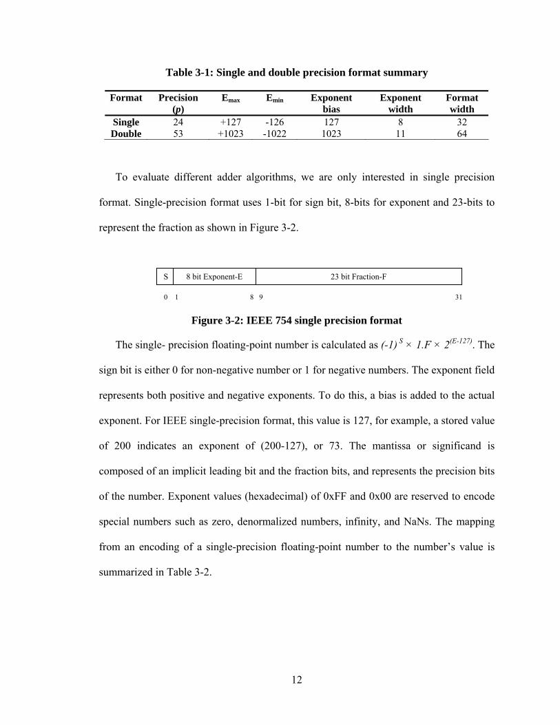
Table 3-1: Single and double precision format summary
Format Precision (p)
Emax Emin Exponent bias
Exponent width
Format width
Single 24 +127 -126 127 8 32 Double 53 +1023 -1022 1023 11 64
To evaluate different adder algorithms, we are only interested in single precision
format. Single-precision format uses 1-bit for sign bit, 8-bits for exponent and 23-bits to
represent the fraction as shown in Figure 3-2.
Figure 3-2: IEEE 754 single precision format
The single- precision floating-point number is calculated as (-1) S × 1.F × 2(E-127). The
sign bit is either 0 for non-negative number or 1 for negative numbers. The exponent field
represents both positive and negative exponents. To do this, a bias is added to the actual
exponent. For IEEE single-precision format, this value is 127, for example, a stored value
of 200 indicates an exponent of (200-127), or 73. The mantissa or significand is
composed of an implicit leading bit and the fraction bits, and represents the precision bits
of the number. Exponent values (hexadecimal) of 0xFF and 0x00 are reserved to encode
special numbers such as zero, denormalized numbers, infinity, and NaNs. The mapping
from an encoding of a single-precision floating-point number to the number’s value is
summarized in Table 3-2.
S 8 bit Exponent-E 23 bit Fraction-F
0 1 8 9 31
13
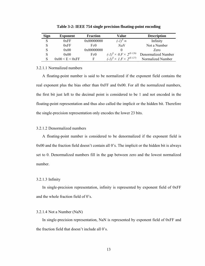
Table 3-2: IEEE 754 single precision floating-point encoding
Sign Exponent Fraction Value Description S 0xFF 0x00000000 (-1)S ∞ Infinity S 0xFF F≠0 NaN Not a Number S 0x00 0x00000000 0 Zero S 0x00 F≠0 (-1)S × 0.F × 2(E-126) Denormalized Number S 0x00 < E < 0xFF F (-1)S × 1.F × 2(E-127) Normalized Number
3.2.1.1 Normalized numbers
A floating-point number is said to be normalized if the exponent field contains the
real exponent plus the bias other than 0xFF and 0x00. For all the normalized numbers,
the first bit just left to the decimal point is considered to be 1 and not encoded in the
floating-point representation and thus also called the implicit or the hidden bit. Therefore
the single-precision representation only encodes the lower 23 bits.
3.2.1.2 Denormalized numbers
A floating-point number is considered to be denormalized if the exponent field is
0x00 and the fraction field doesn’t contain all 0’s. The implicit or the hidden bit is always
set to 0. Denormalized numbers fill in the gap between zero and the lowest normalized
number.
3.2.1.3 Infinity
In single-precision representation, infinity is represented by exponent field of 0xFF
and the whole fraction field of 0’s.
3.2.1.4 Not a Number (NaN)
In single-precision representation, NaN is represented by exponent field of 0xFF and
the fraction field that doesn’t include all 0’s.
14
3.2.1.5 Zero
In single-precision representation, zero is represented by exponent field of 0x00 and
the whole fraction field of 0’s. The sign bit represents -0 and +0, respectively.
3.2.2 Rounding Modes
Rounding takes a number regarded as infinitely precise and, if necessary, modifies it
to fit in the destination’s format while signaling the inexact exception. Thus the rounding
mode affects the results of most arithmetic operations, and the thresholds for overflow
and underflow exceptions. In IEEE 754 floating point representation, there are four
rounding modes defined: round towards nearest even (REN), round towards -∞ (RP),
round towards +∞ (RM), and round towards 0 (RZ). The default rounding mode is REN
and is mostly used in all the arithmetic implementations in software and hardware. In
order to evaluate different adder algorithms, we are also interested in only the default
rounding mode i.e. REN. In this mode, the representable value nearest to the infinitely
precise result is chosen. If the two nearest representable values are equally near, the one
with its least significant bit equal to zero is chosen.
3.2.3 Exceptions
The IEEE 754 defines five types of exceptions: overflow, underflow, invalid
operation, inexact result, and division-by-zero. Exceptions are signaled by setting a flag
or setting a trap. In evaluating hardware implementations of different floating-point adder
algorithms, we only implemented overflow and underflow flags in our designs as they are
the most frequent exceptions that occur during addition.
15
3.2.3.1 Invalid operation
The given operation cannot be performed on the operands. In the case of an adder,
these are the subtraction of infinity or NaN inputs.
3.2.3.2 Inexact result
Inexact exception is set when the rounded result is not exact or it overflows without
an overflow trap. Exact is determined when no precision was lost while performing the
rounding.
3.2.3.3 Division by zero
In the case when the divisor is zero, the result is set to signed ∞.
3.2.3.4 Overflow
Overflow exception is defined by the rounding mode used. In REN, overflow occurs
if the rounded result has an exponent equal to 0xFF or if any of the input operators is
infinity.
3.2.3.5 Underflow
Underflow exception occurs when there is a loss of accuracy. If the implicit bit of the
result is 0 and exponent out is -126 or 0x01, the number is too small to be represented
fully in the single precision format and the underflow flag is set.
3.3 Standard Floating Point Addition Algorithm
This section will review the standard floating point algorithm architecture, and the
hardware modules designed as part of this algorithm, including their function, structure,
16
and use. The standard architecture is the baseline algorithm for floating-point addition in
any kind of hardware and software design [16].
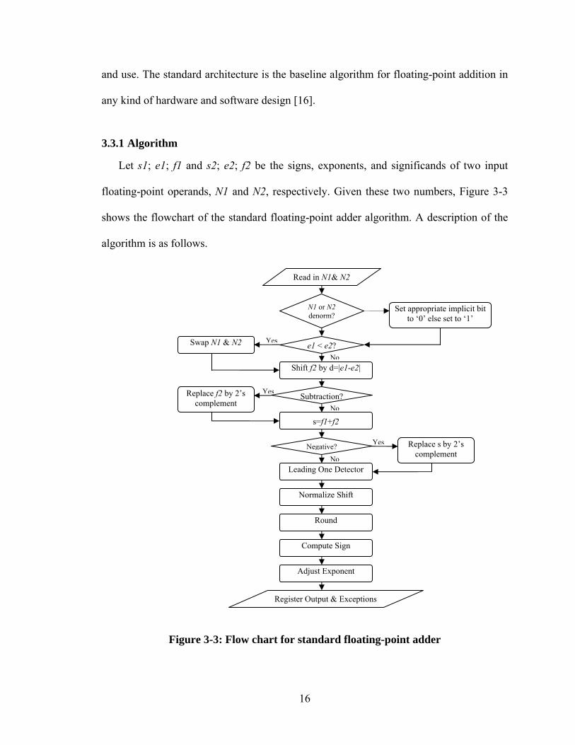
3.3.1 Algorithm
Let s1; e1; f1 and s2; e2; f2 be the signs, exponents, and significands of two input
floating-point operands, N1 and N2, respectively. Given these two numbers, Figure 3-3
shows the flowchart of the standard floating-point adder algorithm. A description of the
algorithm is as follows.
Figure 3-3: Flow chart for standard floating-point adder
N1 or N2 denorm?
Set appropriate implicit bit to ‘0’ else set to ‘1’
e1 < e2?
Shift f2 by d=|e1-e2|
Swap N1 & N2
Replace f2 by 2’s complement
Subtraction?
s=f1+f2
Negative? Replace s by 2’s complement
Leading One Detector
Normalize Shift
Round
Compute Sign
Adjust Exponent
Register Output & Exceptions
Read in N1& N2
No
No
No
Yes
Yes
Yes
17
1. The two operands, N1 and N2 are read in and compared for denormalization and infinity. If numbers are denormalized, set the implicit bit to 0 otherwise it is set to 1. At this point, the fraction part is extended to 24 bits.
2. The two exponents, e1 and e2 are compared using 8-bit subtraction. If e1 is less than e2, N1 and N2 are swapped i.e. previous f2 will now be referred to as f1 and vice versa.
3. The smaller fraction, f2 is shifted right by the absolute difference result of the two exponents’ subtraction. Now both the numbers have the same exponent.
4. The two signs are used to see whether the operation is a subtraction or an addition.
5. If the operation is a subtraction, the bits of the f2 are inverted.
6. Now the two fractions are added using a 2’s complement adder.
7. If the result sum is a negative number, it has to be inverted and a 1 has to be added to the result.
8. The result is then passed through a leading one detector or leading zero counter. This is the first step in the normalization step.
9. Using the results from the leading one detector, the result is then shifted left to be normalized. In some cases, 1-bit right shift is needed.
10. The result is then rounded towards nearest even, the default rounding mode.
11. If the carry out from the rounding adder is 1, the result is left shifted by one.
12. Using the results from the leading one detector, the exponent is adjusted. The sign is computed and after overflow and underflow check, the result is registered.
3.3.2 Micro-Architecture
Using the above algorithm, the standard floating point adder was designed. The
detailed micro-architecture of the design is shown in Figure 3-4. It shows the main
hardware modules necessary for floating-point addition. The detailed description and
functionality of each module will be given later in this chapter.
18
Figure 3-4: Micro-architecture of standard floating-point Adder
The main hardware modules for a single-precision floating-point adder are the
exponent difference module, right shift shifter, 2’s complement adder, leading one
detector, left shift shifter, and the rounding module. The bit-width as shown in Figure 3-4
and following figures is specifically for single-precision addition and will have to be
changed for any other format.
3.3.3 Exponent Difference Module
The exponent difference module has the following two functions:
• To compute absolute difference of two 8-bit numbers.
• To identify if e1 is smaller than e2.
S Exp Mantissa S Exp Mantissa
Exponent Difference
0 1Mux
0 1Mux
Right Shifter
Normalize
Complement
2’s Comp Adder
LOD
Round
Mantissa Out
Cout
Sub
Sign Diff
Add/Sub
Larger exp
Diff
Exp Out
27 27
1
23
5
23
26
58
8
8
8 23
8
2424
27
19
Figure 3-5: Hardware implementation for exponent difference
The hardware implementation of the exponent difference module is shown in Figure
3-5. In order to choose the best adder implementation, four different types of adders,
ripple carry adder, carry-look ahead adder, carry-save adder [18] and VHDL inbuilt adder
were designed to compare the area and timing information and choose the right
implementation for further work. For this purpose, 16 bit test adders with carry-in and
carry-out were implemented. Table 3-3 shows the results compiled using the Xilinx ISE
for Virtex 2p device. Combinational delay is independent of clock and thus is defined as
the total propagation and routing delays of all the gates included in the critical path of the
circuit. Each CLB consists of 4 slices in Virtex2p architecture, and used as the basic unit
of measuring area in Xilinx FPGAs. Both these design parameters are reported by Xilinx
ISE after synthesizing, routing, and placing the circuit onto a FPGA device. The timing
and area information for each module synthesized and placed separately gives a rough
estimation in order to compare different implementations and choose the best one.
However these numbers are not valid when all the modules are connected together to get
the overall delay and area but still the numbers are affected proportionally and thus a
good tool for comparative study.
88
-
e1 e2
0 1
+
81
Sign Difference
Difference
Cout
8
20
Table 3-3: Adder implementation analysis
Adder Type Combinational Delay (ns) Slices Ripple-Carry Adder 15.91 18 Carry-Save Adder 11.951 41
Carry-Look Ahead Adder 9.720 39 VHDL Adder 6.018 8
As it is evident from Table 3-3, the VHDL adder shows the least combinational delay
and area. In adders, the delay is mostly offered due to the propagation of carry. While
designing custom adders, carry-look ahead adder offers the best delay because the carry
is calculated separately looking at the inputs. VHDL adders use the inbuilt carry-chains in
CLBs of the Virtex 2p FPGA and provide very small delay and area and thus are chosen
for all further adder and subtraction implementations. An 8-bit adder is used to subtract
the exponents and the carry out is used to identify if e1 is smaller than e2. If the result is
negative, it has to be complemented and a 1 has to be added to it in order to give out the
absolute difference.
3.3.4 Right Shift Shifter
The right shifter is used to shift right the significand of the smaller operand by the
absolute exponent difference. This is done so that the two numbers have the same
exponent and normal integer addition can be implemented. Right shifter is one of the
most important modules when designing for latency. In order not to loose the precision of
the number, three extra bits, the guard (g), round (r), and sticky (s) are added to the
significand. The g and r bits are first and second bits that might be shifted out and s is the
bit computed by ORing all the other bits that are shifted out. Two different
implementations for the customized right shifter were done and named barrel and align
21
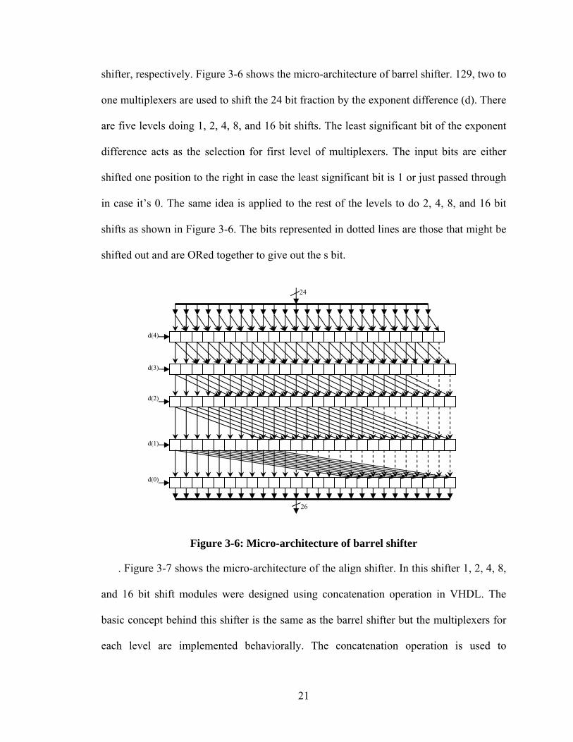
shifter, respectively. Figure 3-6 shows the micro-architecture of barrel shifter. 129, two to
one multiplexers are used to shift the 24 bit fraction by the exponent difference (d). There
are five levels doing 1, 2, 4, 8, and 16 bit shifts. The least significant bit of the exponent
difference acts as the selection for first level of multiplexers. The input bits are either
shifted one position to the right in case the least significant bit is 1 or just passed through
in case it’s 0. The same idea is applied to the rest of the levels to do 2, 4, 8, and 16 bit
shifts as shown in Figure 3-6. The bits represented in dotted lines are those that might be
shifted out and are ORed together to give out the s bit.
Figure 3-6: Micro-architecture of barrel shifter
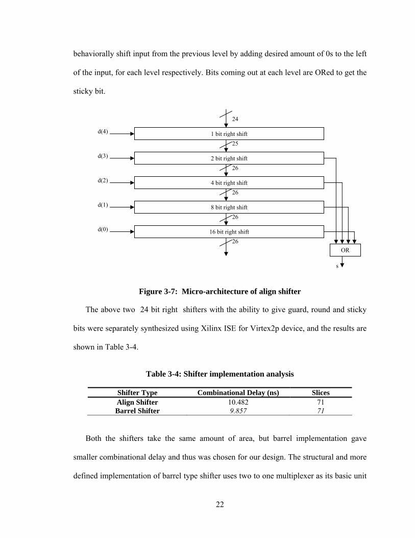
. Figure 3-7 shows the micro-architecture of the align shifter. In this shifter 1, 2, 4, 8,
and 16 bit shift modules were designed using concatenation operation in VHDL. The
basic concept behind this shifter is the same as the barrel shifter but the multiplexers for
each level are implemented behaviorally. The concatenation operation is used to
d(4)
d(3)
d(2)
d(1)
d(0)
24
26
22
behaviorally shift input from the previous level by adding desired amount of 0s to the left
of the input, for each level respectively. Bits coming out at each level are ORed to get the
sticky bit.
Figure 3-7: Micro-architecture of align shifter
The above two 24 bit right shifters with the ability to give guard, round and sticky
bits were separately synthesized using Xilinx ISE for Virtex2p device, and the results are
shown in Table 3-4.
Table 3-4: Shifter implementation analysis
Shifter Type Combinational Delay (ns) Slices Align Shifter 10.482 71 Barrel Shifter 9.857 71
Both the shifters take the same amount of area, but barrel implementation gave
smaller combinational delay and thus was chosen for our design. The structural and more
defined implementation of barrel type shifter uses two to one multiplexer as its basic unit
d(0)
d(1)
d(2)
d(3)
d(4)
s
1 bit right shift
2 bit right shift
4 bit right shift
8 bit right shift
16 bit right shift
OR
24
25
26
26
26
26
23
which is easily synthesizable by the function generators present in the slices. The align
type shifter relies on the synthesizer to implement the behaviorally coded large
multiplexers and thus offers more propagation delay due to added routing.
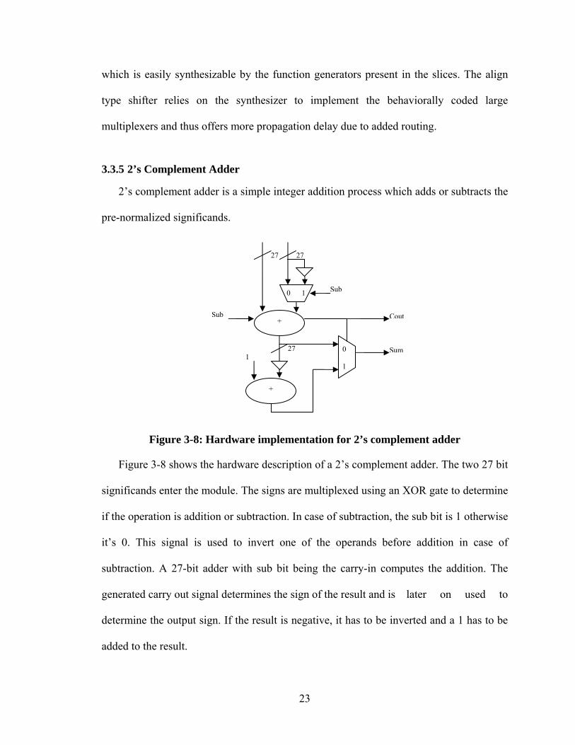
3.3.5 2’s Complement Adder
2’s complement adder is a simple integer addition process which adds or subtracts the
pre-normalized significands.
Figure 3-8: Hardware implementation for 2’s complement adder
Figure 3-8 shows the hardware description of a 2’s complement adder. The two 27 bit
significands enter the module. The signs are multiplexed using an XOR gate to determine
if the operation is addition or subtraction. In case of subtraction, the sub bit is 1 otherwise
it’s 0. This signal is used to invert one of the operands before addition in case of
subtraction. A 27-bit adder with sub bit being the carry-in computes the addition. The
generated carry out signal determines the sign of the result and is later on used to
determine the output sign. If the result is negative, it has to be inverted and a 1 has to be
added to the result.
2727
+
0 1
Sub
Sub
27
Cout
+
10 1
Sum
24
3.3.6 Leading One Detector
After the addition, the next step is to normalize the result. The first step is to identify
the leading or first one in the result. This result is used to shift left the adder result by the
number of zeros in front of the leading one. In order to perform this operation, special
hardware, called Leading One Detector (LOD) or Leading Zero Counter (LZC), has to be
implemented.
There are a number of ways of designing a complex and complicated circuit such as
LOD. A combinational approach is a complex process because each bit of the result is
dependant on all the inputs. This approach leads to large fan-in dependencies and the
resulting design is slow and complicated. Another approach is using Boolean
minimization and Karnaugh map, but the design is again cumbersome and unorganized.
The circuit can also be easily described behaviorally using VHDL and the rest can be left
to Xilinx ISE or any synthesis tool. In our floating-point adder design, we used the LOD
design which identifies common modules and imposes hierarchy on the design. As
compared to other options, this design has low fan-in and fan-out which leads to area and
delay efficient design [17] first presented by Oklobdzija in 1994.
3.3.6.1 Oklobdzija’s LOD
The first step in the design process is to examine two bits case shown in Table 3-5.
The module is named as LOD2. The pattern shows the possible combinations. If the left
most bit is 1, the position bit is assigned 0 and the valid bit is assigned 1. The position bit
is set to 1 if the second bit is 1 and the first bit is 0. The valid bit is set to 0 if both the bits
are 0.
25
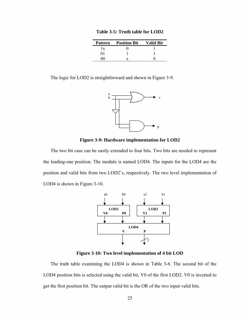
Table 3-5: Truth table for LOD2
Pattern Position Bit Valid Bit 1x 0 1 01 1 1 00 x 0
The logic for LOD2 is straightforward and shown in Figure 3-9.
Figure 3-9: Hardware implementation for LOD2
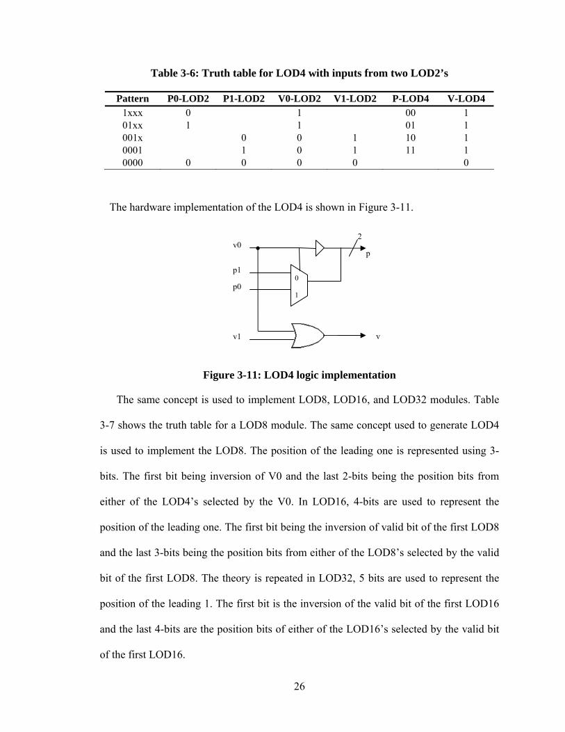
The two bit case can be easily extended to four bits. Two bits are needed to represent
the leading-one position. The module is named LOD4. The inputs for the LOD4 are the
position and valid bits from two LOD2’s, respectively. The two level implementation of
LOD4 is shown in Figure 3-10.
Figure 3-10: Two level implementation of 4 bit LOD
The truth table examining the LOD4 is shown in Table 3-6. The second bit of the
LOD4 position bits is selected using the valid bit, V0 of the first LOD2. V0 is inverted to
get the first position bit. The output valid bit is the OR of the two input valid bits.
ab
p
v
LOD2 V0 P0
LOD2 V1 P1
LOD4 V P
2
a0 b0 a1 b1
26
Table 3-6: Truth table for LOD4 with inputs from two LOD2’s
Pattern P0-LOD2 P1-LOD2 V0-LOD2 V1-LOD2 P-LOD4 V-LOD4 1xxx 0 1 00 1 01xx 1 1 01 1 001x 0 0 1 10 1 0001 1 0 1 11 1 0000 0 0 0 0 0
The hardware implementation of the LOD4 is shown in Figure 3-11.
Figure 3-11: LOD4 logic implementation
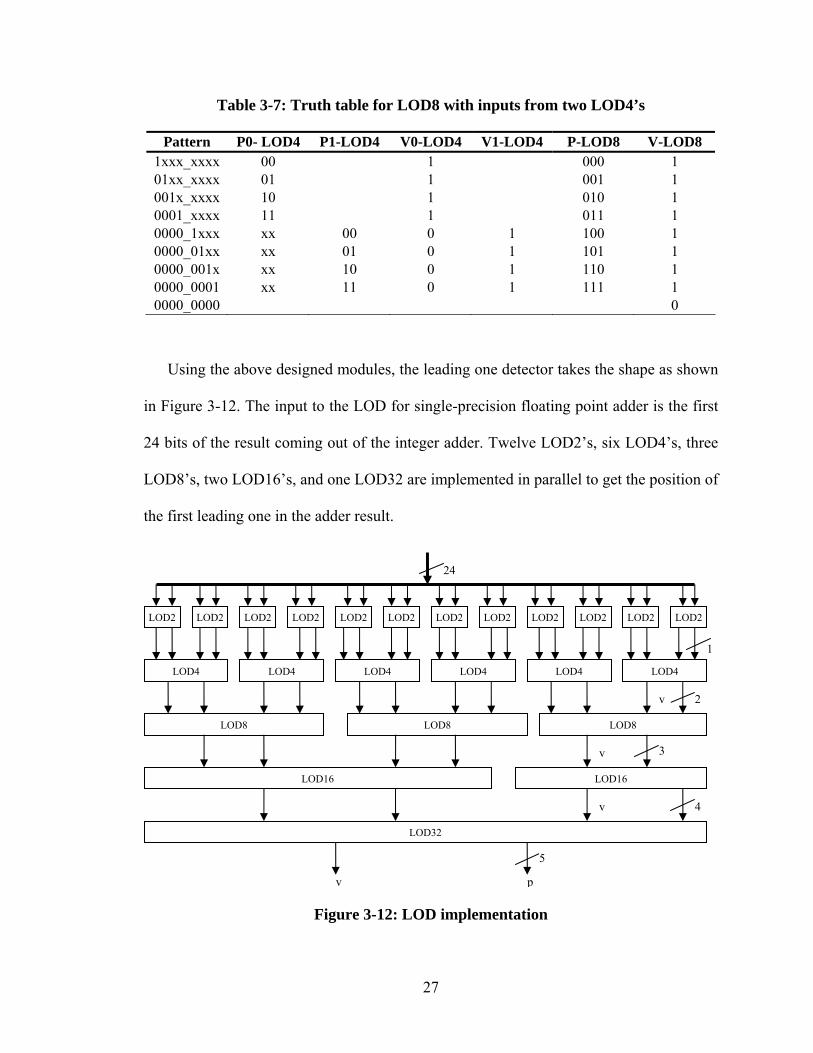
The same concept is used to implement LOD8, LOD16, and LOD32 modules. Table
3-7 shows the truth table for a LOD8 module. The same concept used to generate LOD4
is used to implement the LOD8. The position of the leading one is represented using 3-
bits. The first bit being inversion of V0 and the last 2-bits being the position bits from
either of the LOD4’s selected by the V0. In LOD16, 4-bits are used to represent the
position of the leading one. The first bit being the inversion of valid bit of the first LOD8
and the last 3-bits being the position bits from either of the LOD8’s selected by the valid
bit of the first LOD8. The theory is repeated in LOD32, 5 bits are used to represent the
position of the leading 1. The first bit is the inversion of the valid bit of the first LOD16
and the last 4-bits are the position bits of either of the LOD16’s selected by the valid bit
of the first LOD16.
0 1
p1
p0
v0
v1
p
v
2
27
Table 3-7: Truth table for LOD8 with inputs from two LOD4’s
Pattern P0- LOD4 P1-LOD4 V0-LOD4 V1-LOD4 P-LOD8 V-LOD8 1xxx_xxxx 00 1 000 1 01xx_xxxx 01 1 001 1 001x_xxxx 10 1 010 1 0001_xxxx 11 1 011 1 0000_1xxx xx 00 0 1 100 1 0000_01xx xx 01 0 1 101 1 0000_001x xx 10 0 1 110 1 0000_0001 xx 11 0 1 111 1 0000_0000 0
Using the above designed modules, the leading one detector takes the shape as shown
in Figure 3-12. The input to the LOD for single-precision floating point adder is the first
24 bits of the result coming out of the integer adder. Twelve LOD2’s, six LOD4’s, three
LOD8’s, two LOD16’s, and one LOD32 are implemented in parallel to get the position of
the first leading one in the adder result.
Figure 3-12: LOD implementation
LOD2 LOD2 LOD2 LOD2 LOD2 LOD2 LOD2 LOD2 LOD2 LOD2 LOD2 LOD2
LOD4 LOD4 LOD4 LOD4 LOD4 LOD4
LOD8 LOD8 LOD8
LOD16 LOD16
LOD32
5
4
3
2
1
24
pv
v
v
v
28
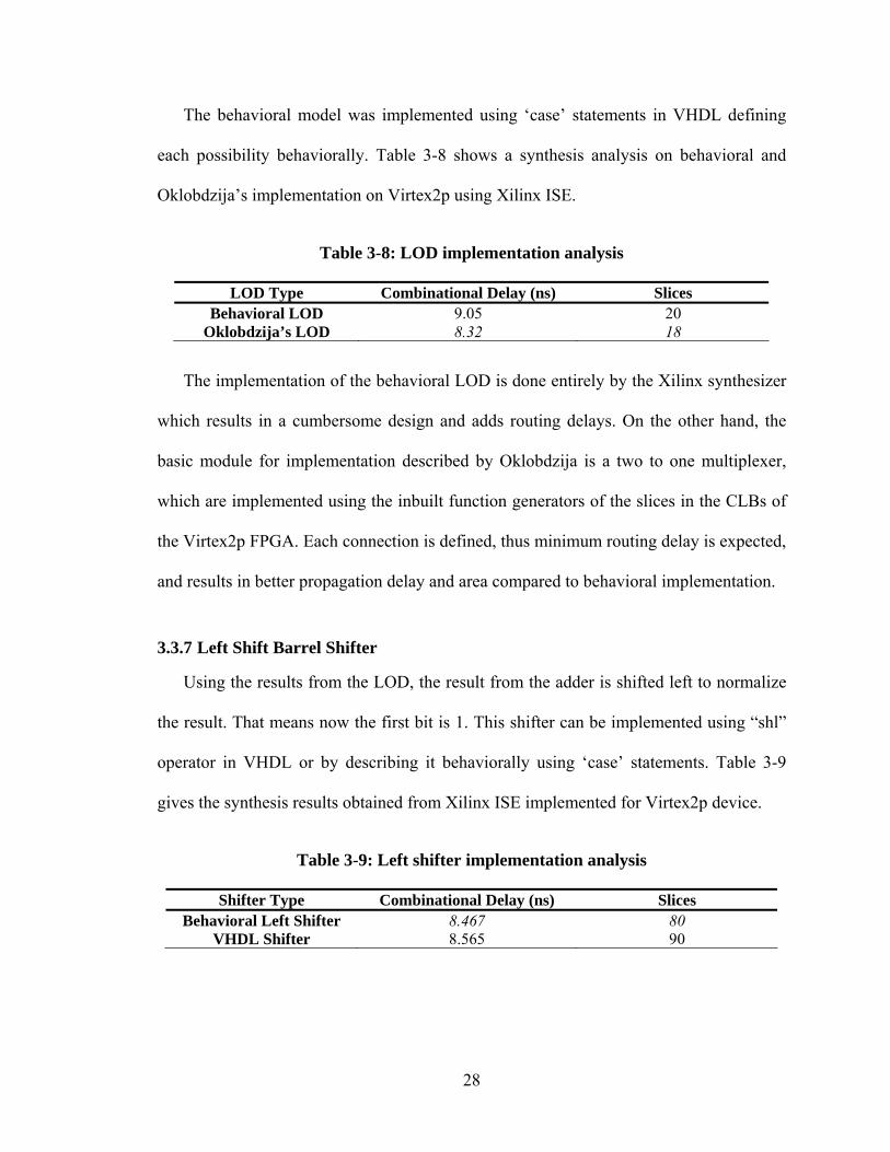
The behavioral model was implemented using ‘case’ statements in VHDL defining
each possibility behaviorally. Table 3-8 shows a synthesis analysis on behavioral and
Oklobdzija’s implementation on Virtex2p using Xilinx ISE.
Table 3-8: LOD implementation analysis
LOD Type Combinational Delay (ns) Slices Behavioral LOD 9.05 20
Oklobdzija’s LOD 8.32 18
The implementation of the behavioral LOD is done entirely by the Xilinx synthesizer
which results in a cumbersome design and adds routing delays. On the other hand, the
basic module for implementation described by Oklobdzija is a two to one multiplexer,
which are implemented using the inbuilt function generators of the slices in the CLBs of
the Virtex2p FPGA. Each connection is defined, thus minimum routing delay is expected,
and results in better propagation delay and area compared to behavioral implementation.
3.3.7 Left Shift Barrel Shifter
Using the results from the LOD, the result from the adder is shifted left to normalize
the result. That means now the first bit is 1. This shifter can be implemented using “shl”
operator in VHDL or by describing it behaviorally using ‘case’ statements. Table 3-9
gives the synthesis results obtained from Xilinx ISE implemented for Virtex2p device.
Table 3-9: Left shifter implementation analysis
Shifter Type Combinational Delay (ns) Slices Behavioral Left Shifter 8.467 80
VHDL Shifter 8.565 90
29
The behavioral model had a negligibly smaller combinational delay, and smaller area,
and is therefore used in our implementation. This result was unexpected because a
behavioral implementation has given a better timing and area numbers compared to the
VHDL operator which uses inbuilt shift registers in the CLBs. For a single precision
floating-point adder the maximum amount of left shift needed is 27. The hardware for the
behavioral left shifter is designed to only accommodate the maximum shift amount. As
we have no control over the hardware implementation in VHDL shifter, it implements
hardware for shift amounts greater than 27, thus resulting in bigger area and delay
compared to behavioral shifter. Only in case when the carry out from the adder is 1 and
the operation is addition, the result is shifted right by one position.
3.3.8 Rounding
Rounding is done using the guard, round and sticky bit of the result. REN mode is
accomplished by rounding up if the guard bit is set, and then pulling down the lowest bit
of the output if the r and s bits are 0. A 1 is added to the result if r and s bit are 1 or r and
either of the last two bits of the normalized result is 1. This step is really important to
assure precision and omit loss of accuracy.
The fraction part of the answer is determined using the rounded result. The exponent
part of the result is determined by subtracting the larger of the exponent by the leading
zero count from the leading one detector, only in case when the result is shifted right in
normalization step or the carry out from rounding adder is 1, a one is added to the
exponent. The sign is selected according to the sign of the result of the integer adder.
Overflow and underflow exceptions are flagged by comparing the output exponent to the
desired conditions explained above.
30
3.3.9 Timing and Area Analysis
The standard single precision floating point adder is synthesized, placed, and routed
for Virtex2p FPGA device using Xilinx ISE 6.3i. The minimum clock period reported by
the synthesis tool after placing and routing was 27.059 ns. The levels of logic reported
were 46. That means the maximum clock speed that can be achieved for this
implementation is 36.95 MHz. The number of slices reported by the synthesis tool was
541. All this information will be used as a base to analyze improved floating-point adder
algorithms. Table 3-10 summarizes these results.
Table 3-10: Standard algorithm analysis
Algorithm Clock period (ns)
Clock speed (MHz)
Area (Slices)
Levels of logic
Standard 27.059 36.95 541 46
3.4 Five Stage Pipeline Standard Floating Point Adder Implementation
In order to decrease clock period, to run the operations at a higher clock rate, and to
increase speedup by increasing the throughput, pipelining is used. Pipelining is achieved
by distributing the hardware into smaller operations, such that the whole operation takes
more clock cycles to complete but new inputs can be added with every clock cycle
increasing the throughput. Pipelining of floating-point adder has been discussed in a
number of previous research papers [9, 10]. Minimum, maximum, and optimum number
of pipeline stages for a 32 bit floating-point number has been given based on the factor of
frequency per area (MHz/Slices). According to these studies, 16 pipeline stages are the
optimum for single-precision adder implementation. In order to achieve this, all of the
hardware modules have to be sub-pipelined within themselves. In order to analyze effects

31
of pipelining on floating-point adder implementations on FPGAs, we will compare our
implementation results with Xilinx IP Core by Digital Core Design [12]. The key features
for the IP given by Digital Core Design are given below:
• Full IEEE-754 compliance
• Single precision real format support
• 5 levels pipeline
• Overflow, underflow and invalid operation flags
• Full accuracy and precision
• Results available at every clock
• Fully synthesizable
• Positive edge clocking and no internal tri-states
Our implementation realizes all the features except the invalid flag.
3.4.1 Micro-Architecture
Figure 3-13 shows the micro-architecture of five stage pipeline implementation of the
standard floating-point adder algorithm implementation. The levels of pipeline chosen are
purely based on comparison with the Xilinx IP Core and are entirely a design choice
according to the design needs. Five is a good choice because anymore stages will need
sub pipelining the modules. The placement of the registers in order to put stages is shown
as the dotted line in Figure 3-13. The main theory behind pipelining is to decrease the
clock period thus increasing the overall clock speed that the application can run. Adding
pipeline stages exploits the D flip-flops in the slices already being used for other logic
and thus doesn’t increase the area significantly. Pipelining also helps increase throughput
as after the first five clock cycles a result is produced after every clock cycle.
32
Figure 3-13: Micro-architecture of 5 stage pipeline standard floating-point adder
In the first stage of the implementation the two operands are compared to identify
denormalization and infinity. Then the two exponents are subtracted to obtain the
exponent difference and identify whether the operands need to be swapped using the
exponent difference sign. In the second stage the right sifter is used to pre normalize the
smaller mantissa. In the third stage addition is done along with the leading one detection.
In the fourth stage left shifter is used to post normalize the result. In the last stage the
exponent out is calculated and rounding is done. The results are then compared to set
overflow or underflow flags.
S Exp Mantissa S Exp Mantissa
Exponent Difference
0 1Mux
0 1Mux
Right Shifter
Normalize
Complement
2’s Comp Adder
LOD
Round
Mantissa Out
Cout
Sub
Sign Diff
Add/Sub
Larger exp
Diff
Exp Out
2727
1
23
23
26
5
8
8
8
823
8
24 24
27
33
3.4.2 Timing and Area Comparison with Xilinx Intellectual Property
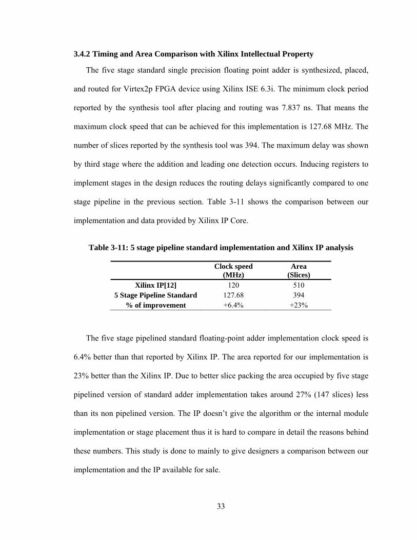
The five stage standard single precision floating point adder is synthesized, placed,
and routed for Virtex2p FPGA device using Xilinx ISE 6.3i. The minimum clock period
reported by the synthesis tool after placing and routing was 7.837 ns. That means the
maximum clock speed that can be achieved for this implementation is 127.68 MHz. The
number of slices reported by the synthesis tool was 394. The maximum delay was shown
by third stage where the addition and leading one detection occurs. Inducing registers to
implement stages in the design reduces the routing delays significantly compared to one
stage pipeline in the previous section. Table 3-11 shows the comparison between our
implementation and data provided by Xilinx IP Core.
Table 3-11: 5 stage pipeline standard implementation and Xilinx IP analysis
Clock speed (MHz)
Area (Slices)
Xilinx IP[12] 120 510 5 Stage Pipeline Standard 127.68 394
% of improvement +6.4% +23%
The five stage pipelined standard floating-point adder implementation clock speed is
6.4% better than that reported by Xilinx IP. The area reported for our implementation is
23% better than the Xilinx IP. Due to better slice packing the area occupied by five stage
pipelined version of standard adder implementation takes around 27% (147 slices) less
than its non pipelined version. The IP doesn’t give the algorithm or the internal module
implementation or stage placement thus it is hard to compare in detail the reasons behind
these numbers. This study is done to mainly to give designers a comparison between our
implementation and the IP available for sale.
34
3.5 Conclusion
In this chapter, the IEEE 754 standard for floating-point representation is explained in
detail. After this, the architecture and hardware implementation of standard or naive
floating-point adder algorithm is illustrated. Logic implementation of each hardware
module is discussed and analyzed. The timing and area information gathered by Xilinx
synthesis tool is summarized. In the end the standard algorithm is pipelined in five stages
and compared with the area and timing information provided by Xilinx IP.
35
CHAPTER 4 IMPROVED FLOATING-POINT ADDER
ALGORITHMS
This chapter goes over the two main improvements made to the standard floating-
point adder algorithm. The first is named the LOP algorithm and the second one is the far
and close data-path algorithm. The central concept behind the first improvement is in
terms of latency by introducing parallelism within floating-point adder modules. The
second improvement is done by having dedicated paths for two different cases, because
not all hardware modules are needed for all input operands. Both these improvements add
significant area compared to the standard floating-point adder but decrease the latency.
In modern hardware applications, latency is the most important parameter for most
operations. While designing for FPGA devices with millions of reconfigurable hardware
gates, area can be given up to gain overall latency. Pipelining is another technique used to
increase the overall throughput of the adder but doesn’t decrease the latency. In this
chapter, pipelining and its effects on far and close data-path adder implementation will
also be discussed.
4.1 Leading One Predictor Algorithm
In this section, LOP implementation and its use in floating-point addition is described
in detail. LOP module is also used in far and close data-path algorithm implementation.
36
Figure 4-1: a) Leading one detector b) Leading one prediction
Figure 4-1 shows the difference between leading one detection and prediction. LOD
detects leading one after the adder result is available. On the other hand, LOP is used to
predict the leading one in parallel with the adder computation. This decreases the number
of logic levels in the critical path and results in an overall improvement in the latency.
Figure 4-2: Micro-architecture of LOP algorithm adder
LOP
24
S Exp Mantissa S Exp Mantissa
Exponent Difference
0 1Mux
0 1Mux
Right Shifter
Normalize
Complement
2’s Comp Adder
Round
Mantissa Out
Cout
Sub
sign_d
Add/Sub
Larger exp
Diff
Exp Out
27 27
1
23
27
23
26
58
8
8
823
8
2424
5
24
Adder
LOD Adder LOP
a) b)
37
Figure 4-2 shows the micro-architecture of LOP algorithm and is close to that of the
standard floating-point implementation. The inputs to the adder also enter the LOP, so
that the position of the leading one can be computed in parallel with the addition process.
This result is then used in post-normalization process and computing the resulting
exponent.
4.1.1 Leading One Predictor
The LOP consists of three operations [3, 21]:
• Pre-encoding the inputs
• Leading one detection
• Error correction in case of some situations
There are three ways to design a leading one predictor. The first architecture doesn’t
have a concurrent correction and uses a compensate shift during normalization, and the
second one has a concurrent error detection based on carry checking. The third one which
we used is with concurrent correction based on parallel detection tree. Parallel, leading
one detection and correction adds area to the design but decreases the overall latency of
the module by reducing levels of logic.
For a single-precision floating-point addition operation, a 24-bit LOP is needed. A
and B are the two inputs, the leading one predictor designed is for A > B and/or A < B.
This is needed because even after pre-normalization, the resulting addition can be
negative as in case of A < B. When the effective operation is addition, the LOP result is
not used and the shift value is always zero. The general structure is shown in Figure 4-3.
38
Figure 4-3: General structure of LOP
4.1.2 Pre-Encoding Logic
The pre-encoding module gives a string of 0s and 1s with the location of the first one
being the leading one position. After this, the leading one detector already designed for
standard algorithm is used to compute the position of the most significant bit. This is the
amount we need to shift for normalization, in case of no correction. The pre-encoding
module also gives strings of symbols, which are passed through the binary tree to
determine if correction is needed. A one is added to the leading one position if a certain
string of symbols is identified.
In order to get the string of 0s and 1s, to pass through the LOD, first the following
logic has to be encoded for all input bits where ‘i’ is the number of bits being encoded.
iii b1 when ae ==
iii ba when1g >=
iii ba when1s <=
The string which will be the input to LOD is then calculated using the following
logic:
24
Pre-encoding logic
For leading one detector
For concurrent correction
24
LOD Error detection tree
Correction Shift value
f
39
)gg s(se )g s s(ge f 1ii1ii1-i1ii1ii1-ii +⋅+⋅+⋅+⋅ +++= (4.1)
To detect the error, inputs are encoded for positive and negative cases separately.
These inputs will act as the initial inputs to the binary trees to detect the correction
pattern. In the case when A > B, the encodings for detection tree inputs are defined as:
i1iii i n s ) s(g p ⋅⋅+= +
i1-i i se n ⋅= (4.2)
ii i n p z +=
In the case when A < B, the encodings for detection tree inputs are defined as:
i1iii i p g ) s(g n ⋅⋅+= +
i1-i i ge p ⋅= (4.3)
ii i n p z +=
Using the above equations, hardware for the pre-encoder is entered in VHDL using
AND, OR and NOT gates. Equations 4.2 and 4.3 are different than those provided by J.
D. Bruguera and T. Lang [3]. For a respective set of input bits, only pi or ni can be set to 1
in positive and negative cases. A NAND gate has to be added to pi and ni for positive and
negative trees respectively to obtain the right inputs for the error detection step. This
error was notified and acknowledged by the authors.
4.1.3 Leading One Detector
The same leading one detector used in the standard floating-point adder is used for
the leading one detection. The string ‘f’ computed using the encodings shown in equation
4.1, is used as the input. The output is the shift amount needed to normalize the result
40
from the adder. In this case this operation is done in parallel to addition and thus
decreases levels of logic in the critical path.
4.1.4 Correction Tree
In order to detect an error, pre-encoded values shown in equations 4.2 and 4.3 are
passed through a binary tree structure to determine whether the correction pattern is
present. The general structure of the correction tree is shown in Figure 4-4.
Figure 4-4: General structure of error correction tree
The positive and negative trees consist of nodes to detect if a certain string is present.
If zkpzqn(x) is detected in case of A > B, the inputs to LOP, and zknzqp(x) in case of A <
B then a 1 has to be added to the result from LOD. The values of z, p and n are obtained
from equations 4.2 and 4.3, respectively; k and q can be any integer value.
4.1.4.1 Positive tree
The values from the pre-encoder module are passed through a binary tree. The nodes
of the binary tree consist of logic to detect certain strings and have five possible values Z,
P, N, Y, and U representing the following substrings.
Pre-encoding logic for concurrent correction
Positive encoding Negative encoding
a b2424
Positive
Tree
Negative
Tree
Correction pattern present
n p z n p z
41
Z zk
P zkpzq
N zkn(x)
Y zkpzqn(x)
U other strings
The outputs from two consecutive nodes of the preceding level become inputs to the
next as shown in Figure 4-5. The first level has its inputs coming from the pre-encoder
block as shown in Figure 4-4 and is encoded by logic given in equation 4.2. Table 4-1
shows the node function for positive tree error correction. If string Y is detected in the
last level, node correction is needed.
Table 4-1: Node function for positive tree error detection
Second Input Z2 P2 N2 Y2 U2
Z1 Z P N Y U P1 P U Y U U N1 N N N N N Y1 Y Y Y Y Y
First Input
U1 U U U U U
Using the node function, the following equations are derived and implemented, where
Z1, Z2, P1, P2, N1, N2, Y1, and Y2 are inputs to the node.
Z2Z1= Z ⋅
Z2)(P1 P2)(Z1P ⋅+⋅= (4.4)
N2) (Z1 N1N ⋅+=
N2) (P1 Y2) (Z1 Y1Y ⋅+⋅+=
42
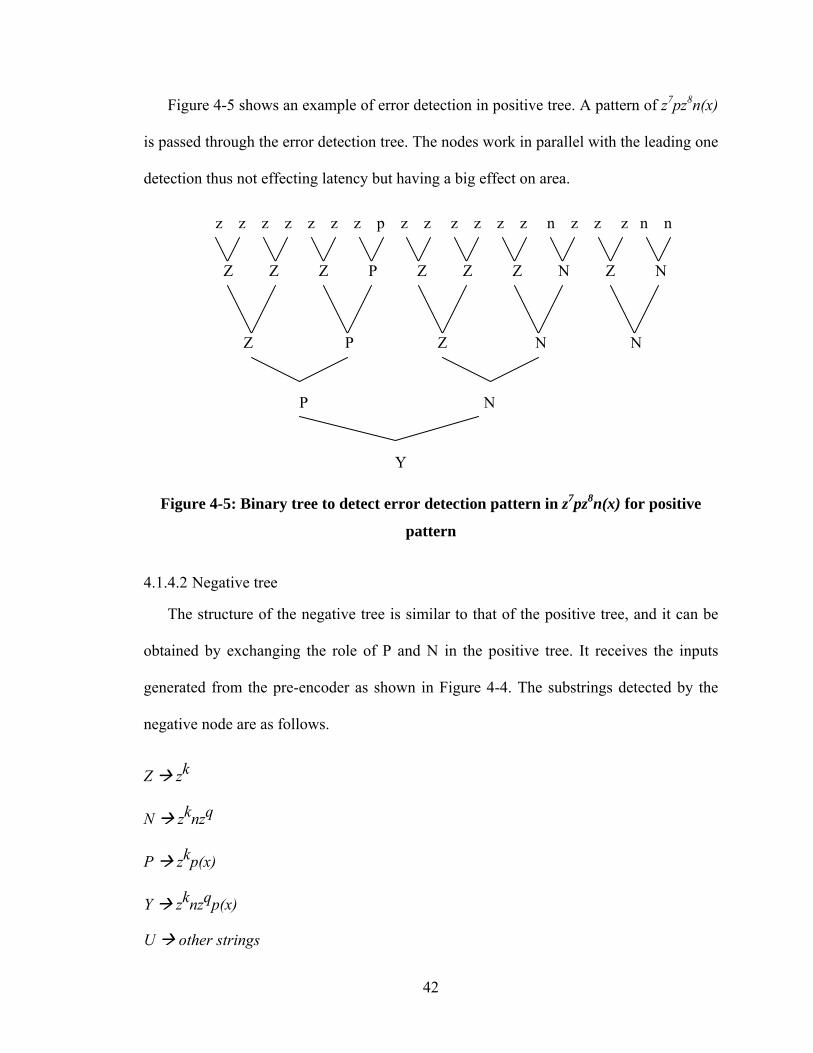
Figure 4-5 shows an example of error detection in positive tree. A pattern of z7pz8n(x)
is passed through the error detection tree. The nodes work in parallel with the leading one
detection thus not effecting latency but having a big effect on area.
Figure 4-5: Binary tree to detect error detection pattern in z7pz8n(x) for positive
pattern
4.1.4.2 Negative tree
The structure of the negative tree is similar to that of the positive tree, and it can be
obtained by exchanging the role of P and N in the positive tree. It receives the inputs
generated from the pre-encoder as shown in Figure 4-4. The substrings detected by the
negative node are as follows.
Z zk
N zknzq
P zkp(x)
Y zknzqp(x)
U other strings
z z z z z z z p z z z z z z n z z z n n
Y
Z Z Z P Z Z Z N Z N
Z P Z N N
P N
43
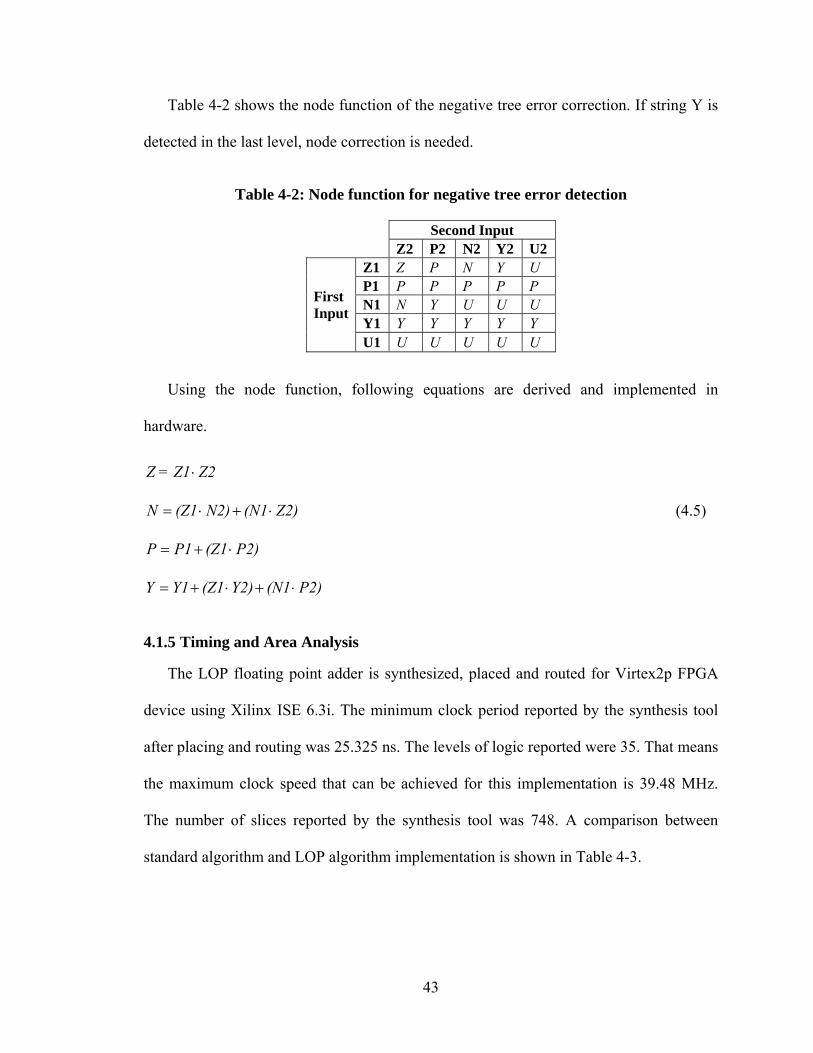
Table 4-2 shows the node function of the negative tree error correction. If string Y is
detected in the last level, node correction is needed.
Table 4-2: Node function for negative tree error detection
Second Input Z2 P2 N2 Y2 U2
Z1 Z P N Y U P1 P P P P P N1 N Y U U U Y1 Y Y Y Y Y
First Input
U1 U U U U U
Using the node function, following equations are derived and implemented in
hardware.
Z2Z1= Z ⋅
Z2)(N1 N2)(Z1N ⋅+⋅= (4.5)
P2) (Z1 P1P ⋅+=
P2) (N1 Y2) (Z1 Y1Y ⋅+⋅+=
4.1.5 Timing and Area Analysis
The LOP floating point adder is synthesized, placed and routed for Virtex2p FPGA
device using Xilinx ISE 6.3i. The minimum clock period reported by the synthesis tool
after placing and routing was 25.325 ns. The levels of logic reported were 35. That means
the maximum clock speed that can be achieved for this implementation is 39.48 MHz.
The number of slices reported by the synthesis tool was 748. A comparison between
standard algorithm and LOP algorithm implementation is shown in Table 4-3.
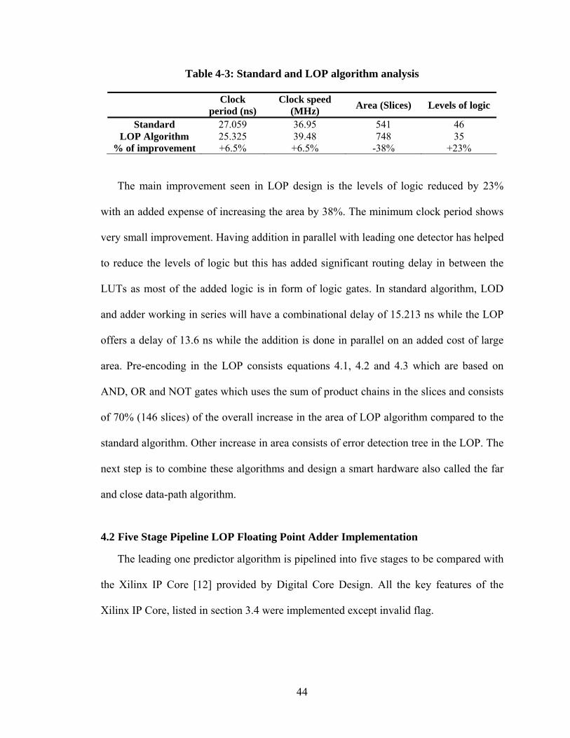
44
Table 4-3: Standard and LOP algorithm analysis
Clock period (ns)
Clock speed (MHz) Area (Slices) Levels of logic
Standard 27.059 36.95 541 46 LOP Algorithm 25.325 39.48 748 35
% of improvement +6.5% +6.5% -38% +23%
The main improvement seen in LOP design is the levels of logic reduced by 23%
with an added expense of increasing the area by 38%. The minimum clock period shows
very small improvement. Having addition in parallel with leading one detector has helped
to reduce the levels of logic but this has added significant routing delay in between the
LUTs as most of the added logic is in form of logic gates. In standard algorithm, LOD
and adder working in series will have a combinational delay of 15.213 ns while the LOP
offers a delay of 13.6 ns while the addition is done in parallel on an added cost of large
area. Pre-encoding in the LOP consists equations 4.1, 4.2 and 4.3 which are based on
AND, OR and NOT gates which uses the sum of product chains in the slices and consists
of 70% (146 slices) of the overall increase in the area of LOP algorithm compared to the
standard algorithm. Other increase in area consists of error detection tree in the LOP. The
next step is to combine these algorithms and design a smart hardware also called the far
and close data-path algorithm.
4.2 Five Stage Pipeline LOP Floating Point Adder Implementation
The leading one predictor algorithm is pipelined into five stages to be compared with
the Xilinx IP Core [12] provided by Digital Core Design. All the key features of the
Xilinx IP Core, listed in section 3.4 were implemented except invalid flag.
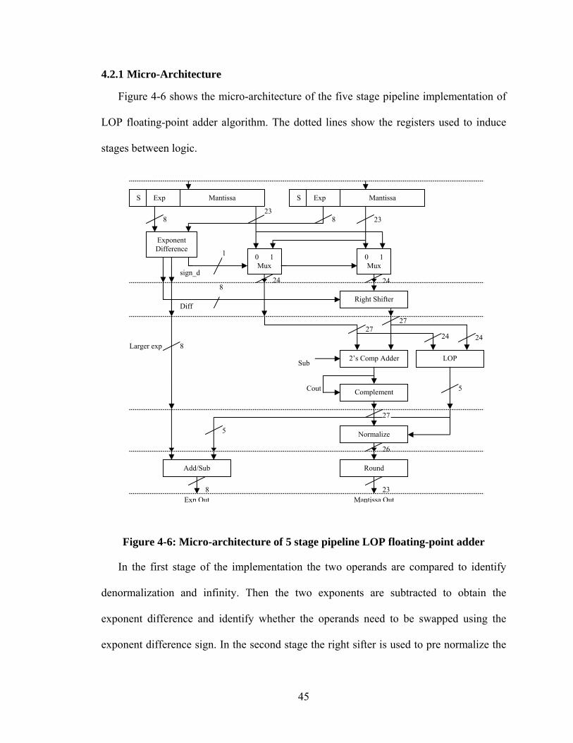
45
4.2.1 Micro-Architecture
Figure 4-6 shows the micro-architecture of the five stage pipeline implementation of
LOP floating-point adder algorithm. The dotted lines show the registers used to induce
stages between logic.
Figure 4-6: Micro-architecture of 5 stage pipeline LOP floating-point adder
In the first stage of the implementation the two operands are compared to identify
denormalization and infinity. Then the two exponents are subtracted to obtain the
exponent difference and identify whether the operands need to be swapped using the
exponent difference sign. In the second stage the right sifter is used to pre normalize the
LOP
24
S Exp Mantissa S Exp Mantissa
Exponent Difference
0 1Mux
0 1Mux
Right Shifter
Normalize
Complement
2’s Comp Adder
Round
Mantissa Out
Cout
Sub
sign_d
Add/Sub
Larger exp
Diff
Exp Out
27 27
1
23
27
23
26
5
8
8
8
8 23
8
24 24
5
24
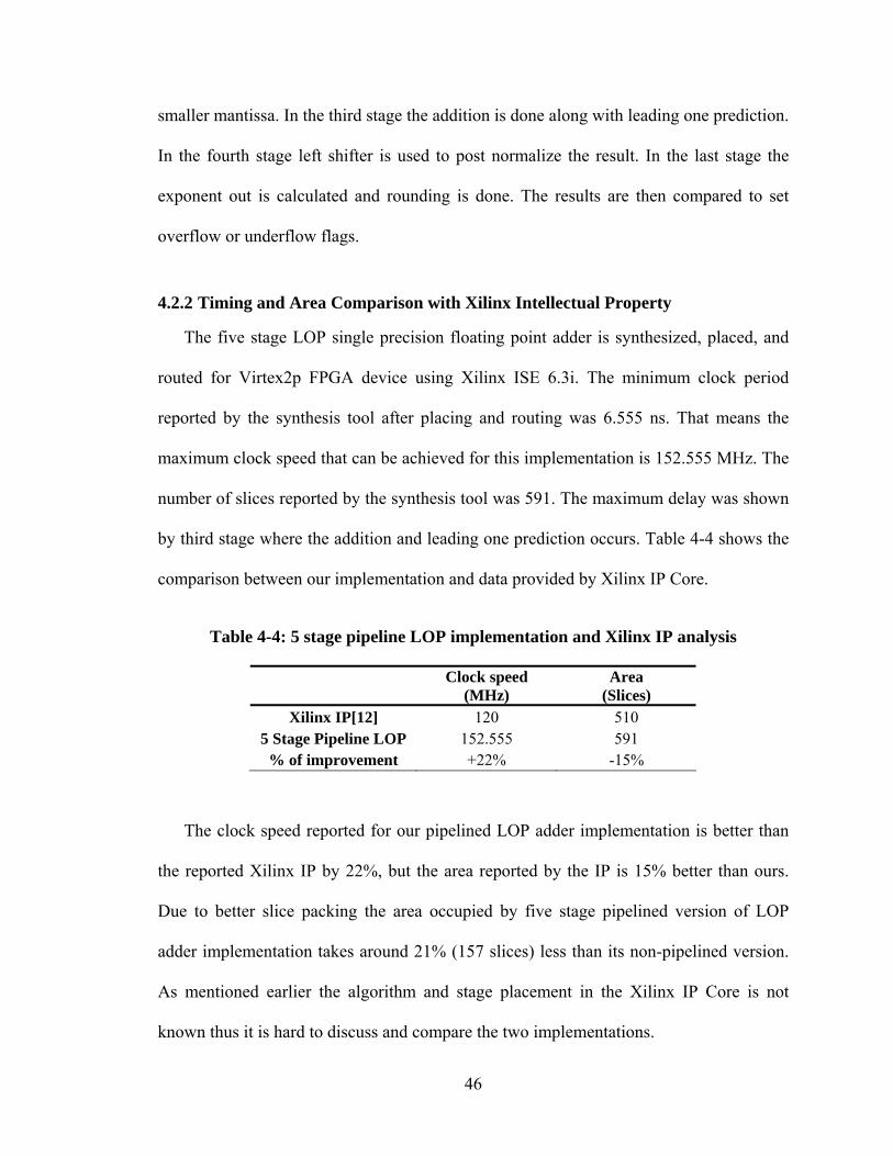
46
smaller mantissa. In the third stage the addition is done along with leading one prediction.
In the fourth stage left shifter is used to post normalize the result. In the last stage the
exponent out is calculated and rounding is done. The results are then compared to set
overflow or underflow flags.
4.2.2 Timing and Area Comparison with Xilinx Intellectual Property
The five stage LOP single precision floating point adder is synthesized, placed, and
routed for Virtex2p FPGA device using Xilinx ISE 6.3i. The minimum clock period
reported by the synthesis tool after placing and routing was 6.555 ns. That means the
maximum clock speed that can be achieved for this implementation is 152.555 MHz. The
number of slices reported by the synthesis tool was 591. The maximum delay was shown
by third stage where the addition and leading one prediction occurs. Table 4-4 shows the
comparison between our implementation and data provided by Xilinx IP Core.
Table 4-4: 5 stage pipeline LOP implementation and Xilinx IP analysis
Clock speed (MHz)
Area (Slices)
Xilinx IP[12] 120 510 5 Stage Pipeline LOP 152.555 591
% of improvement +22% -15%
The clock speed reported for our pipelined LOP adder implementation is better than
the reported Xilinx IP by 22%, but the area reported by the IP is 15% better than ours.
Due to better slice packing the area occupied by five stage pipelined version of LOP
adder implementation takes around 21% (157 slices) less than its non-pipelined version.
As mentioned earlier the algorithm and stage placement in the Xilinx IP Core is not
known thus it is hard to discuss and compare the two implementations.
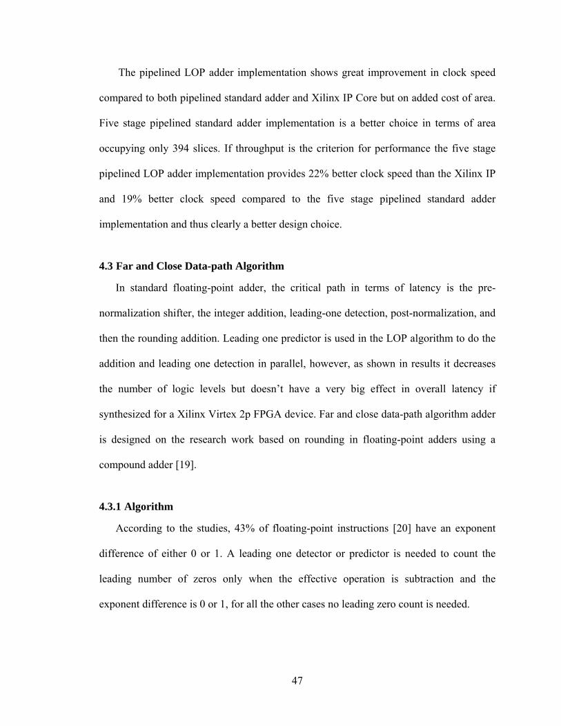
47
The pipelined LOP adder implementation shows great improvement in clock speed
compared to both pipelined standard adder and Xilinx IP Core but on added cost of area.
Five stage pipelined standard adder implementation is a better choice in terms of area
occupying only 394 slices. If throughput is the criterion for performance the five stage
pipelined LOP adder implementation provides 22% better clock speed than the Xilinx IP
and 19% better clock speed compared to the five stage pipelined standard adder
implementation and thus clearly a better design choice.
4.3 Far and Close Data-path Algorithm
In standard floating-point adder, the critical path in terms of latency is the pre-
normalization shifter, the integer addition, leading-one detection, post-normalization, and
then the rounding addition. Leading one predictor is used in the LOP algorithm to do the
addition and leading one detection in parallel, however, as shown in results it decreases
the number of logic levels but doesn’t have a very big effect in overall latency if
synthesized for a Xilinx Virtex 2p FPGA device. Far and close data-path algorithm adder
is designed on the research work based on rounding in floating-point adders using a
compound adder [19].
4.3.1 Algorithm
According to the studies, 43% of floating-point instructions [20] have an exponent
difference of either 0 or 1. A leading one detector or predictor is needed to count the
leading number of zeros only when the effective operation is subtraction and the
exponent difference is 0 or 1, for all the other cases no leading zero count is needed.
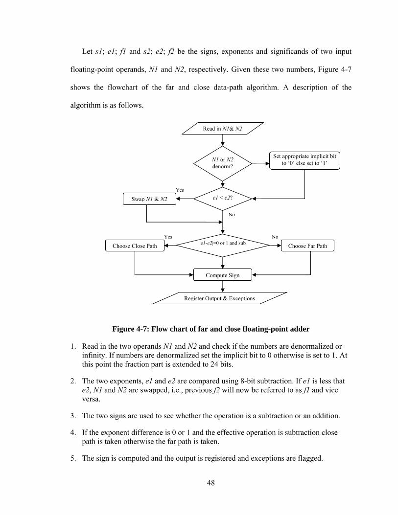
48
Let s1; e1; f1 and s2; e2; f2 be the signs, exponents and significands of two input
floating-point operands, N1 and N2, respectively. Given these two numbers, Figure 4-7
shows the flowchart of the far and close data-path algorithm. A description of the
algorithm is as follows.
Figure 4-7: Flow chart of far and close floating-point adder
1. Read in the two operands N1 and N2 and check if the numbers are denormalized or infinity. If numbers are denormalized set the implicit bit to 0 otherwise is set to 1. At this point the fraction part is extended to 24 bits.
2. The two exponents, e1 and e2 are compared using 8-bit subtraction. If e1 is less that e2, N1 and N2 are swapped, i.e., previous f2 will now be referred to as f1 and vice versa.
3. The two signs are used to see whether the operation is a subtraction or an addition.
4. If the exponent difference is 0 or 1 and the effective operation is subtraction close path is taken otherwise the far path is taken.
5. The sign is computed and the output is registered and exceptions are flagged.
N1 or N2 denorm?
Set appropriate implicit bit to ‘0’ else set to ‘1’
e1 < e2? Swap N1 & N2
Choose Close Path |e1-e2|=0 or 1 and sub
Read in N1& N2
No
No
Yes
Yes
Choose Far Path
Compute Sign
Register Output & Exceptions
49
Figure 4-8 shows the micro-architecture of the far and close path floating point adder.
The exponent difference and swap units for pre-normalization are the same as in the
standard or LOP algorithm. The two fractions, exponent difference, and larger exponent
are the common inputs to both the paths. Close path is chosen if the exponent difference
is 0 or 1 and the effective operation is a subtraction otherwise the far path is chosen. The
close and far path will be explained in detail in the following sections.
4.3.2 Micro-Architecture
Figure 4-8: Micro-architecture of far and close path floating-point adder
4.3.3 Close Path Micro-architecture
In order to reduce the latency added by rounding adder, compound adder which
outputs sum (S) and sum plus one (S1) is implemented. One of them is chosen to
Exp & mantissa out (close)
S Exp Mantissa S Exp Mantissa
Exponent Difference
0 1Mux
0 1 Mux
Sign Diff
1
23 8 23
8
24 24
Far Path
Close Path Sub
Larger exp
Diff
0 1Mux
Path
3030Exp & mantissa out (far)
Exp & mantissa out
Cout
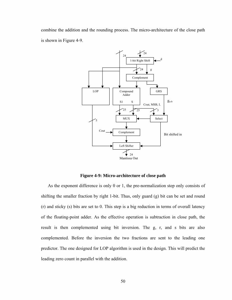
50
combine the addition and the rounding process. The micro-architecture of the close path
is shown in Figure 4-9.
Figure 4-9: Micro-architecture of close path
As the exponent difference is only 0 or 1, the pre-normalization step only consists of
shifting the smaller fraction by right 1-bit. Thus, only guard (g) bit can be set and round
(r) and sticky (s) bits are set to 0. This step is a big reduction in terms of overall latency
of the floating-point adder. As the effective operation is subtraction in close path, the
result is then complemented using bit inversion. The g, r, and s bits are also
complemented. Before the inversion the two fractions are sent to the leading one
predictor. The one designed for LOP algorithm is used in the design. This will predict the
leading zero count in parallel with the addition.
1-bit Right Shift
Left Shifter
Complement
Compound Adder
S1 S
LOP
Cout
24
24
2424
5
2525
Complement
g
GRS
Select
ga-b
3
Cout, MSB, L
MUX
Bit shifted in
Mantissa Out
d
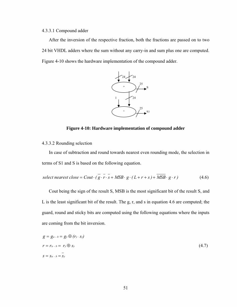
51
4.3.3.1 Compound adder
After the inversion of the respective fraction, both the fractions are passed on to two
24 bit VHDL adders where the sum without any carry-in and sum plus one are computed.
Figure 4-10 shows the hardware implementation of the compound adder.
Figure 4-10: Hardware implementation of compound adder
4.3.3.2 Rounding selection
In case of subtraction and round towards nearest even rounding mode, the selection in
terms of S1 and S is based on the following equation.
)rgMSB)srL(g MSB srg( Coutclose nearest select ⋅⋅+++⋅⋅+⋅⋅⋅= (4.6)
Cout being the sign of the result S, MSB is the most significant bit of the result S, and
L is the least significant bit of the result. The g, r, and s in equation 4.6 are computed; the
guard, round and sticky bits are computed using the following equations where the inputs
are coming from the bit inversion.
yb-a
yyb-a
yyyb-a
s ss
sr rr
)s(r ggg
==
⊕==
⊕== ⋅
(4.7)
2424
+ S
24
+
1
S125
25
52
As in the case of subtraction, 1 has to be added to sticky location to obtain 2’s
complement. Equation 4.7 is used to induce a 1 at the sticky location. We also have to
consider a carry from this addition of 1 to the least significant bit of S. If there is such a
carry, the g, r, and s bits computed using equation 4.7 are all 0s. If the result is positive
i.e. carry-out is 1 then in this case S1 is chosen to compensate this carry but no rounding
up is needed. This is the first addend in equation 4.6. The sum result is normalized when
most significant bit of the adder result is 1 and g, r, and s bits are not 0 meaning no carry
from the addition of 1 in the sticky bit position. Rounding is needed if sum result is
positive, normalized and if the g bit is 1 and either of the least significant bit, r, or s bit is
1. S1 is selected in this case to round the result. This is the second addend to equation 4.6.
In the case when result is positive and the result is not normalized, S1 is chosen to round
to nearest only when both g and r bits are 1. This is the third addend in equation 4.6. As
in close path both r and s bits are 0, equation 4.6 can be reduced to following.
)L MSBg( Coutclose nearest select ⋅+⋅= (4.8)
Thus, equation 4.8 is used to select between the results of S1 or S outputs from the
compound adder. This step reduces the extra delay induced by the rounding adder in
standard and LOP algorithm.
4.3.3.3 Post-normalization
After the rounded result has been selected, using equation 4.8, the LOP result is
needed to normalize the result by left shifting the result by the shift amount predicted.
Before this step, the result is inverted if the result is negative i.e. carry-out is 0. The first
bit shifted in is 1 only when the result is positive and g bit is 1, otherwise all the bits
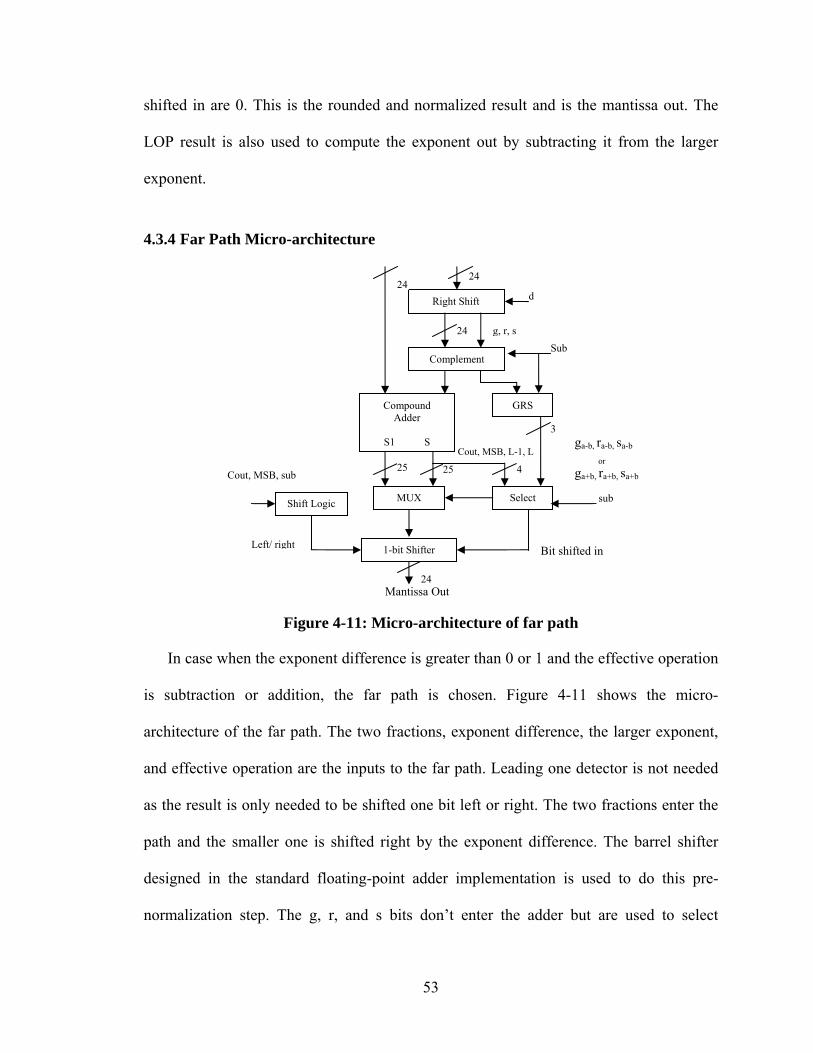
53
shifted in are 0. This is the rounded and normalized result and is the mantissa out. The
LOP result is also used to compute the exponent out by subtracting it from the larger
exponent.
4.3.4 Far Path Micro-architecture
Figure 4-11: Micro-architecture of far path
In case when the exponent difference is greater than 0 or 1 and the effective operation
is subtraction or addition, the far path is chosen. Figure 4-11 shows the micro-
architecture of the far path. The two fractions, exponent difference, the larger exponent,
and effective operation are the inputs to the far path. Leading one detector is not needed
as the result is only needed to be shifted one bit left or right. The two fractions enter the
path and the smaller one is shifted right by the exponent difference. The barrel shifter
designed in the standard floating-point adder implementation is used to do this pre-
normalization step. The g, r, and s bits don’t enter the adder but are used to select
Right Shift
1-bit Shifter
Shift Logic
Compound Adder
S1 S
Cout, MSB, sub
24
24
2424
2525
Complement
g, r, s
GRS
Select
ga-b, ra-b, sa-b
or ga+b, ra+b, sa+b 4
Cout, MSB, L-1, L
MUX
Bit shifted in
Mantissa Out
d
Sub
3
sub
Left/ right
54
between S1 and S of the compound adder like the close path implementation. After the
pre-normalization step, the results enter the compound adder and compute sum and sum
plus one as discussed earlier. In case of subtraction the shifted fraction is inverted.
4.3.4.1 Rounding selection
In case of addition and round towards nearest even rounding mode, the selection in
terms of S1 and S is based on the following equation.
s)rg1-(LLCouts)r(Lg Coutfar nearest select +++⋅⋅+++⋅⋅= (4.9)
In case of subtraction, the selection in terms of S1 and S is based on the following
equation.
s)) (Lg MSB rg srg( Coutfar nearest select +⋅⋅+⋅+⋅⋅⋅= (4.10)
In case of addition there is no change to the g, r, and s bits, but when the effective
operation is subtraction, equation 4.7 is used to compute the added 1 at the sticky bit.
Equation 4.10 has the same explanation of choosing between S1 and S as in the close
path. In case of addition, S1 is chosen to round to nearest if the result is normalized i.e.
carry-out is 0 and if the g bit is 1 and any of the r, s, or the least significant bit of the
adder result is 1. This is the first addend to equation 4.9. If the carry-out of the result is 1
then it is not normalized and it will be right shifted to be normalized. In this case, bit next
to the least significant bit (L-1) is also considered. This is the second addend to the
equation 4.9. Using the above equations and explanation, rounded result is selected from
the compound adder.
55
4.3.4.2 Post-normalization
In case of far path, only 1 bit left or right shift is needed. 1-bit right shift is done if the
result from the adder is not normalized and the effective operation is addition. On the
other hand, 1 bit left shift is needed if the most significant bit of the result is 0 and
subtraction was carried out. This is a big reduction in the critical path in terms of latency
when compared to standard or LOP algorithm implementations. In case of right shift, one
is added to the larger exponent to obtain exponent out, on the other hand, one is
subtracted from the larger exponent in case of left shift.
4.3.5 Sign Computation
In order to compute the sign in far and close path, following conditions are
considered. In case of addition:
sign(N1)sign =
In case of subtraction:
)1N(signsign:)1rencesign_diffe(2e1e
Cout sign(N1) sign:0)difference 0,fferencee2(sign_die1
sign(N1) sign:) 0erence(sign_diff e2e1
==<
⊕====
==>
N1 and N2 are the two operands, but referred vice-versa when swapping occurs as
shown in Figure 4-7. In case of addition, the sign is simply the sign of the first operand,
on the other hand in case of subtraction, the sign is MUXed if result of the adder is
negative or swapping occurs before pre-normalization step.
56
4.3.6 Timing and Area Analysis
The far and close data-path floating point adder is synthesized, placed, and routed for
Virtex2p FPGA device using Xilinx ISE. The minimum clock period reported by the
synthesis tool after placing and routing was 21.821 ns. The levels of logic reported were
30. That means the maximum clock speed that can be achieved for this implementation is
45.82 MHz. The number of slices reported by the synthesis tool was 1018. A comparison
between standard algorithm and far and close data-path algorithm implementation is
shown in Table 4-6.
Table 4-5: Standard and far and close data-path algorithm analysis
Clock Period (ns)
Clock speed (MHz)
Area (Slices) Levels of logic
Standard 27.059 36.95 541 46 F&C path 21.821 45.82 1018 30
% of improvement +19% +19% -88% +34%
A comparison between LOP algorithm and far and close data-path algorithm
implementation is shown in Table 4-7.
Table 4-6: LOP and far and close data-path algorithm analysis
Clock Period (ns)
Clock speed (MHz)
Area (Slices) Levels of logic
LOP 25.325 39.48 748 35 F&C path 21.821 45.82 1018 30
% of improvement +14% +14% -36% +14%
In terms of latency far and close path algorithm shows a 19% improvement compared
to standard algorithm, and 14% improvement compared to the LOP algorithm. In terms
of levels of logic there is a 34% improvement compared to the standard algorithm and
14% improvement compared to the LOP algorithm. When compared to standard
57
algorithm far and close critical path consists of a LOP in parallel with an adder instead of
a LOD followed by an adder in the standard algorithm. The critical path also has only one
full shifter instead of two full shifters in the standard algorithm implementation. In the far
and close data-path algorithm, the compound adder combines addition and rounding steps
and thus eliminates additional delay caused by rounding adder. When compared to LOP
algorithm, far and close critical path contains one less shifter and no rounding adder in its
critical path. On the other hand, in terms of area it is 88% bigger compared to the
standard algorithm but 36% bigger compared to the LOP algorithm.
Figure 4-12 shows the graphical comparison between the latency and area of the three
different floating-point adder algorithms implemented for Virtex2p FPGA device. It is
obvious from the results that for an area efficient design standard algorithm
implementation should be preferred but in case of latency far and close path has much
better results compared to the rest, although on added expense of area.
0200400600800
10001200
Standard LOP F&C path
Slic
es
01020304050
MH
z
Area (Slices) Clock Speed(MHz)
Figure 4-12: Latency and area comparison
58
4.4 Conclusion
In this chapter, the improvements in basic floating point adder algorithms are
discussed. The first change implemented is the leading one predictor algorithm, which
has a great effect on area but doesn’t improve timing significantly, due to added routing
and gate delays in FPGAs. In far and close data-path algorithm implementation, LOP
along with combined addition and rounding, and only one full shift in its critical path
shows significant improvement in the overall latency of the adder. Five stage LOP
pipeline adder implementation is also discussed with its comparison with Xilinx IP core
and five stage pipeline standard adder algorithm implementation.
This chapter gives the designer the choice to select appropriate implementation
according to their design needs. Standard floating-point addition algorithm is meant for
area efficient designs where designers are working with small FPGA devices with very
few equivalent logic gates to fit in their design. For latency efficient designs where the
main aim is to have faster execution units, far and close data-path algorithm is the best
option. It takes almost double the area that of standard algorithm implementation but
gives 19% improvement in overall latency with respect to standard algorithm and 14%
improvement compared to LOP algorithm. When it comes to comparing the pipelined
versions of the algorithms, LOP is the best choice running at around 152 MHz for five
pipeline stages i.e. 22% faster than the Xilinx IP and 19% better than the pipelined
standard adder algorithm implementation. Far and close data-path was not chosen for the
five stage pipeline implementation as the optimum number of stages is either three
without sub pipelining the internal modules [22] or six with the sub staging of the
modules according to our experiment.
59
CHAPTER 5 VERIFICATION AND VALIDATION
This chapter goes over the testing procedure, simulation, and hardware verification of
floating-point adder implementations. In order to verify the hardware implementations,
test benches were developed using Java programming language and simulations were run
using ModelSim for Xilinx [23]. Hardware verification was done using inbuilt Random
Access Memory (RAM) blocks.
5.1 Test Bench
The industry standard to test and obtain performance results for floating-point
arithmetic is SpecFP2000 [24]. Due to lack of resources and unavailability of these test
benches, custom test benches were developed using Java programming language. Java
was chosen because it has inbuilt float class which includes conversion from float data
type to integer and then to hexadecimal format for easy test runs. Some of the other
functions used were Java’s random number generator and for loops.
In Java, the data type float represents a single precision floating point number which
adheres to all the IEEE 754 standard restrictions and round the number to REN which has
been used in our implementations. The class Float has inbuilt function
Float.floatToRawIntBits() which convert any floating point number to integer
representation according to the IEEE 754 standard. Integer.toHexString() is used to
60
covert integers into hexadecimal format. These functions are used to convert it for
binary representation in form of hexadecimal numbers.
Figure 5-1: Example Java test bench developer loop code
In order to generate random numbers, class Math with inbuilt function
Math.random() was used to generate a float number between decimal 0 and 1. A unique
number is generated every time as it based on a seed from the internal clock of the
computer. Multiple ‘for’ loops were used to multiply this number with diverse numbers
public static void main(String[] args) { float rand1, rand2, add; int out_rand1, out_rand2, out_add; String Str, Str2, opa, opb, result, ans, run; char end; int i, j; opa = "force opa X"; opb = "force opb X"; result = "force ans X"; end = '"'; run = "run"; for(i=10000; i<10010; i++) { for (j = 1000000000; j < 1000000001; j++) { rand1 = - (float) Math.random() * i; rand2 = + (float) Math.random() * j; add = rand1 + rand2; out_rand1 = Float.floatToRawIntBits(rand1); Str = Integer.toHexString(out_rand1); System.out.print(opa); System.out.print(end); System.out.print(Str); System.out.println(end); out_rand2 = Float.floatToRawIntBits(rand2); Str2 = Integer.toHexString(out_rand2); System.out.print(opb); System.out.print(end); System.out.print(Str2); System.out.println(end); out_add = Float.floatToRawIntBits(add); ans = Integer.toHexString(out_add); System.out.print(result); System.out.print(end); System.out.print(ans); System.out.println(end); System.out.println(run); }
61
in multiple of 10s to generate two totally different random numbers with different ranges
of exponents to be added. An example java loop is shown in Figure 5-1.
The result is changed into binary form too using the above used functions rounded
towards nearest even and ready to be compared against the answer we obtain from our
implementations. Main emphasis was given on having inputs with diverse exponent
differences and different signs. In order to do an exhaustive test of the hardware, we need
millions of inputs; since this was impossible but using smart loops around 8000 different
inputs were generated. Apart from these special cases which included NaN, zero, and
infinity, cases which give overflow and underflow results were also included in the test
bench.
5.2 Verification of Simulation
ModelSim for Xilinx is a powerful simulation tool developed by Model Technologies
for Xilinx devices. VHDL code can be compiled and special libraries for Xilinx devices
can be used to simulate any hardware efficiently. All the basic modules designed for
standard, LOP, and far and close data-path algorithm were compiled and tested
vigorously for functional correctness using waveforms. The test bench developed using
Java was run under simulation environment for all the three algorithms separately.
Figure 5-2: Example ModelSim run for floating-point adder
62
The results stored in the test bench and the ones obtained from hardware for a certain
pair of inputs were compared bit by bit and 100% accuracy was reported for all cases.
An example test run is shown in Figure 5-2. The numbers are shown are in hexadecimal
format and represent inputs, outputs and the forced result. This step was important to
ensure the functional correctness and robustness of the design.
5.3 Hardware Validation
In order to validate the design on the hardware, the multimedia board (DO-V2000-
MLTA), the only Xilinx board with a Virtex 2 FPGA chip on it was used. Two separate
RAM blocks available in the FPGA were used to store a set of inputs at the same address
location and the addition result was stored in another RAM at the same address location.
The embedded development kit available to us was used to program the FPGA to output
a 1 on the screen if the result registered by the hardware was the same for a certain set of
inputs and its corresponding result obtained from the RAM. This was a custom testing
procedure to ensure that the hardware designed is synthesizable and downloadable onto a
FPGA device. The clock was simulated using a button rather than using the inbuilt clock
to see the results visually. 100% accuracy for all the three algorithms was obtained and
thus the test was considered successful.
63
CHAPTER 6 CONCLUSION
Floating-point unit is an integral part of any modern microprocessor. With
advancement in FPGA architecture, new devices are big and fast enough to fit and run
modern microprocessors interfaced on design boards for different applications. Floating-
point units are available in forms of intellectual property for FPGAs to be bought and
used by customers. However, the HDL for the design is not available to be modified by
the customers according to their design needs. Floating-point adder is the most complex
component of the floating-point unit. It consists of many complex sub components and
their implementations have a major effect on latency and area of the overall design.
Over the past two decades, a lot of research has been done by the VLSI community to
improve overall latency for the floating-point adder while keeping the area reasonable.
Many algorithms have been developed over time. Standard, LOP, and far and close data-
path are the three most common algorithms. In order to reduce confusions among
programmers and vendors, IEEE introduced the IEEE 754 standard in 1985 which
standardizes floating-point binary arithmetic for both software and hardware.
There are many floating-point adder implementations available for FPGAs but to the
best of our knowledge, no work has been done to design and compare different
implementations for each sub component used in the floating-point addition for a FPGA
device. The main objective of our work was to implement these components and obtain
64
best overall latency for the three different algorithms and provide HDL and discuss
solutions to improve custom designs.
Standard algorithm consists of the basic operation which consists of right shifter, 2’s
complement adder, leading one detector, and left shifter. Different implementations for
all these various components were done using VHDL and then synthesized for Xilinx
Virtex 2p FPGA device to be compared for combinational delay and area. The objective
was to reduce the overall latency; therefore each sub component is selected accordingly.
Standard algorithm is also considered as naive algorithm for floating-point adder and is
considered to be area efficient but has larger delays in levels of logic and overall latency.
For a Xilinx Virtex2p FPGA device our implementation of the standard algorithm
occupied 541 slices and had an overall delay of 27.059 ns. The standard algorithm was
also pipelined into five stages to run at 127 MHz which took an area of 394 slices.
The second implementation researched and implemented was the LOP algorithm. It
consists of a module called leading one predictor which has the capability to detect the
leading one and add the normalized operands in parallel. This has a significant effect on
the levels of logic and reduces them by 23% but only reduces the latency by 6.5% on an
added area of 38% compared to the standard algorithm implementation. It is not an
effective design in case of FPGAs because the added slices due to LOP uses SOP chains
present in the CLBs of the Virtex 2p and adds significant routing and gate delay. The
LOP algorithm was also pipelined into five stages to run at 152 MHz which took 591
slices. The pipelined version of LOP adder was a better choice when compared to Xilinx
IP Core [12] running at 22% better clock speed and thus giving a better throughput.
65
The third and most up-to-date implementation mostly employed by all the modern
microprocessors is the far and close data-path algorithm. This algorithm distributes the
design into two paths called the close and far path. The main objective for this algorithm
is to reduce overall latency by reducing the numbers of logics for the two paths by
eliminating or distributing modules only needed in certain cases. This design, as
expected, gives very good latency results on added cost of almost double the area
compared to that of the standard algorithm. For a Xilinx Virtex2p FPGA device our
implementation of the far and close data-path algorithm occupied 1018 slices and had an
overall delay of 21.821 ns.
The main objective of this research was to develop a design resource for designers to
implement floating-point adder onto FPGA device according to their design needs such
as clock speed, throughput and area. This kind of work has not been done before, to the
best of our knowledge, and we believe it would be a great help in custom implementation
and design of floating-point adders on FPGAs.
6.1 Future Work
In order to expand our research further some of the works proposed are converting the
VHDL so that it can accommodate any exponent and mantissa length. This will give the
designer more versatility while choosing their design specs. The designs can also be
pipelined further for different number of pipeline stages to give designers even more
adaptability and flexibility.
66
REFERENCES
[1] M. Farmland, “On the Design of High Performance Digital Arithmetic Units, “ PhD
thesis, Stanford University, Department of Electrical Engineering, August 1981.
[2] P. M. Seidel, G. Even, “Delay-Optimization Implementation of IEEE Floating-Point
Addition,” IEEE Transactions on computers, pp. 97-113, February 2004, vol. 53, no.
2.
[3] J. D. Bruguera and T. Lang, “Leading-One Prediction with Concurrent Position
Correction,” IEEE Transactions on Computers, pp. 1083–1097, 1999, vol. 48, no.10.
[4] S. F. Oberman, H. Al-Twaijry and M. J. Flynn, “The SNAP Project: Design of
Floating-Point Arithmetic Units” Proc. 13th IEEE Symp. on Computer Arithmetic, pp.
156-165, 1997.
[5] Xilinx, http://www.xlinix/com.
[6] L. Louca, T. A. Cook, W. H. Johnson, “Implementation of IEEE Single Precision
Floating Point Addition and Multiplication on FPGAs,” FPGAs for Custom
Computing, 1996.
[7] W. B. Ligon, S. McMillan, G. Monn, F. Stivers, and K. D. Underwood, “A Re-
evaluation of the Practicality of Floating-point Operations on FPGAs,” IEEE Symp.
On Field-Programmable Custom Computing Machines, pp. 206–215, April 1998.
67
[8] E. Roesler, B. E. Nelson, “Novel Optimizations for Hardware Floating-Point Units in
a Modern FPGA Architecture,” Field-Programmable Logic and Applications, pp. 637-
646, September 2002.
[9] J. Liang, R. Tessier and O. Mencer, “Floating Point Unit Generation and Evaluation
for FPGAs,” IEEE Symp. on Field-Programmable Custom Computing Machines, pp.
185-194, April 2003.
[10] G. Govindu, L. Zhuo, S. Choi, and V. Prasanna, “Analysis of High-Performance
Floating-Point Arithmetic on FPGAs,” International Parallel and Distributed
Processing Symp., pp. 149b, April 2004.
[11] A. Malik and S. Ko, “Efficient Implementation of Floating Point Adder using
pipelined LOP in FPGAs,” IEEE Canadian Conference on Electrical and Computer
Engineering, pp. 688-691, May 2005.
[12] Digital Core Design, http://www.dcd.pl/
[13] Quixilica, http://www.quixilica.com/
[14] Nallatech, http://www.nallatech.com/
[15] IEEE Standard Board and ANSI, “IEEE Standard for Binary Floating-Point
Arithmetic,” 1985, IEEE Std 754-1985.
[16] J. Hennessy and D. A. Peterson, Computer Architecture a Quantitative Approach,
Morgan Kauffman Publishers, second edition, 1996.
68
[17] V. G. Oklobdzija, “An Algorithmic and Novel Design of a Leading Zero Detector
Circuit: Comparison with Logic Synthesis.” IEEE Transactions on Very Large Scale
Integration (VLSI) Systems, pp. 124-128, 1994, Vol. 2, No. 1.
[18] Israel Koren, Computer Arithmetic Algorithms, A K Peters, second edition, 2002.
[19] J. D. Bruguera and T. Lang,“Rounding in Floating-Point Addition using a
Compound Adder,” University of Santiago de Compostela, Spain Internal Report, July
2000.
[20] M. J. Flynn, S. F. Oberman, Advanced Computer Arithmatic Design. John Wiley &
Sons, Inc, 2001.
[21] M. J. Flynn, “Leading One Prediction -- Implementation, generalization, and
application,” Technical Report: CSL-TR-91-463, March 1991.
[22] S. F. Oberman, “Design Issues in High performance floating-point arithmetic units,”
Technical Report: CSL-TR-96-711, December 1996.
[23] http://www.model.com/
[24] http://www.spec.org/
[25] N. Shirazi, A. Walters, P. M. Athanas, “Quantitative analysis of floating point
arithmetic on FPGA based custom computing machines”. IEEE Symp. on Field-
Programmable Custom Computing Machines, pp. 155-163, 1995.
69
APPENDIX
VHDL CODE
Standard Algorithm LIBRARY ieee ; USE ieee.std_logic_1164.ALL; USE ieee.std_logic_misc.ALL; USE ieee.std_logic_unsigned.ALL; USE ieee.std_logic_arith.ALL; entity fpad is port( clk: in std_logic; opa: in std_logic_vector (0 to 31); opb: in std_logic_vector (0 to 31); add: out std_logic_vector(0 to 31); underflow: out std_logic; overflow: out std_logic); end fpad ; architecture arch of fpad is signal opa_r, opb_r: std_logic_vector(0 to 31); signal signa, signb: std_logic; signal expa, expb: std_logic_vector(0 to 7); signal fraca, fracb: std_logic_vector(0 to 23); signal a_exp_zero, b_exp_zero: std_logic; signal a_exp_ones, b_exp_ones: std_logic; signal a_frac_zero, b_frac_zero: std_logic; signal denorm_a, denorm_b: std_logic; signal a_zero, b_zero: std_logic; signal a_inf, b_inf: std_logic; signal signd: std_logic; signal swap: std_logic; signal signx: std_logic; signal expx: std_logic_vector(0 to 7); signal fracx, fracy: std_logic_vector(0 to 23); signal rsft_amt: std_logic_vector(0 to 7); signal modeslct: std_logic; signal fracy_in_sft, align_fracy: std_logic_vector(0 to 26); signal sub:std_logic; signal a, b, sum_adder: std_logic_vector(0 to 26); signal cout_adder, neg_sum: std_logic; signal lzc: std_logic_vector(0 to 4); signal lsft_amt: std_logic_vector(0 to 7); signal rsft1: std_logic; signal lrsft_in: std_logic_vector(0 to 27); signal lrsft1_out: std_logic_vector(0 to 25); signal norm_sft_out: std_logic_vector(0 to 26); signal norm: std_logic_vector(0 to 25); signal norm_out: std_logic_vector(0 to 23); signal r, s, round: std_logic; signal round_out: std_logic_vector(0 to 24); signal round_cout: std_logic;
70
signal mantissa: std_logic_vector(0 to 23); signal exponent: std_logic_vector(0 to 7); signal sign, uf, ovf: std_logic; component exp_diff port ( exp_a, exp_b: in std_logic_vector(0 to 7); d: out std_logic_vector(0 to 7); sign_d: out std_logic); end component; component bshifter_rt is port ( i: in std_logic_vector(0 to 26); sftamt: in std_logic_vector(0 to 4); o: out std_logic_vector(0 to 26)); end component; component adder is port( a, b: in std_logic_vector(0 to 26); sub:in std_logic; sum: out std_logic_vector(0 to 26); cout: out std_logic); end component; component lrsft1 is port ( i: in std_logic_vector (0 to 27 ); lsft, rsft: in std_logic; o: out std_logic_vector (0 to 25)); end component; component bshifter_lft is port ( i: in std_logic_vector (0 to 26 );--input sft_amt: in std_logic_vector (0 to 7 );--shift amount o: out std_logic_vector (0 to 26));--shift answer, g r and s bits end component; component lod is port ( f: in std_logic_vector(0 to 23); d: out std_logic_vector(0 to 4)); end component; begin process (clk) begin if clk='1' and clk'event then opa_r<=opa; opb_r<=opb; end if; end process;
71
a_exp_zero<=not (or_reduce(opa_r(1 to 8))); b_exp_zero<=not (or_reduce(opb_r(1 to 8))); a_exp_ones<=and_reduce(opa_r(1 to 8)); b_exp_ones<=and_reduce(opb_r(1 to 8)); a_frac_zero<=not (or_reduce(opa_r(9 to 31))); b_frac_zero<=not (or_reduce(opb_r(9 to 31))); denorm_a<= a_exp_zero and (not a_frac_zero); denorm_b<= b_exp_zero and (not b_frac_zero); a_zero<=a_exp_zero and a_frac_zero; b_zero<=b_exp_zero and b_frac_zero; a_inf<=a_exp_ones and a_frac_zero; b_inf<=b_exp_ones and b_frac_zero; signa<= opa_r(0); expa<= opa_r(1 to 8) when denorm_a='0' else x"01"; fraca<=('0' & opa_r(9 to 31)) when (denorm_a='1' or a_zero='1') else ('1' & opa_r(9 to 31)); signb<= opb_r(0); expb<= opb_r(1 to 8) when denorm_b='0' else x"01"; fracb<=('0' & opb_r(9 to 31)) when (denorm_b='1' or b_zero='1') else ('1' & opb_r(9 to 31)); exp_diff1: exp_diff port map(expa, expb, rsft_amt, signd);--exponent difference swap<=signd; expx<=expa when swap='0' else expb; fracx<=fraca when swap='0' else fracb; fracy<=fracb when swap='0' else fraca; modeslct<=or_reduce(rsft_amt(0 to 6));--0 when ex-ey<=1, 1 otherwise fracy_in_sft<=fracy & "000"; bshfiter_rt1: bshifter_rt port map (fracy_in_sft, rsft_amt(3 to 7), align_fracy); a<=fracx & "000"; b<=align_fracy(0 to 26); sub<= signa xor signb;--0 for addition, 1 for subtraction adder1: adder port map(a, b, sub, sum_adder, cout_adder); neg_sum<=cout_adder and sub; rsft1<= cout_adder and (not sub); lrsft_in<=(not (cout_adder & sum_adder) + "000000000000000000000000001") when neg_sum='1' else (cout_adder & sum_adder); lod1: lod port map(lrsft_in(1 to 24), lzc); lsft_amt<="000" & lzc; --if modeslct=1 ex-ey>1 normalization shifter consist of maximmim 1 left shift --if modeslct=0 ex-ey<=1 an there was a carry_out normalization shifter consist of 1 right shift lrsft1_1: lrsft1 port map(lrsft_in, lsft_amt(7), rsft1, lrsft1_out); bshifter_lft1: bshifter_lft port map(lrsft_in(1 to 27), lsft_amt, norm_sft_out); norm<=lrsft1_out(0 to 25) when (modeslct or rsft1)='1' else (norm_sft_out(0 to 24) & or_reduce(norm_sft_out(25 to 26))); norm_out<=norm(0 to 23); r<=norm(24); s<=norm(25); round<=(r and s) or (r and norm_out(23)); round_out<=(('0' & norm_out) + "0000000000000000000000001") when round='1' else ('0' & norm_out); round_cout<=round_out(0); mantissa<=(round_cout & round_out(1 to 23)) when round_cout='1' else round_out(1 to 24); exponent<=(expx + x"01") when (rsft1 or round_cout)='1' else (expx - lsft_amt); uf<='1' when exponent=x"01" and mantissa(0)='0' else '0'; ovf<='1' when exponent=x"FF" or a_inf='1' or b_inf='1' else '0'; signx<=signb when swap='1' or neg_sum='1' else signa; sign<=signx;
72
process (clk) begin if clk='1' and clk'event then add<=sign & exponent & mantissa(1 to 23); underflow<=uf; overflow<=ovf; end if; end process; end arch; 5 Stages Pipeline Standard Algorithm entity fpad_p is port( clk: in std_logic; opa: in std_logic_vector (0 to 31);--input operators opb: in std_logic_vector (0 to 31); add: out std_logic_vector(0 to 31); underflow: out std_logic; overflow: out std_logic); end fpad_p ; architecture arch of fpad_p is signal opa_r, opb_r: std_logic_vector(0 to 31); signal signa_r, signb_r, swap_r, a_inf_r, b_inf_r: std_logic; signal expx_r: std_logic_vector(0 to 7); signal fracy_in_sft_r: std_logic_vector(0 to 26); signal rsft_amt_r: std_logic_vector(0 to 7); signal fracx_r: std_logic_vector(0 to 23); signal signa_r_r, signb_r_r, modeslct_r, swap_r_r, sub_r, a_inf_r_r, b_inf_r_r: std_logic; signal a_r, b_r: std_logic_vector(0 to 26); signal expx_r_r: std_logic_vector(0 to 7); signal lrsft_in_r: std_logic_vector(0 to 27); signal lsft_amt_r: std_logic_vector(0 to 7); signal rsft1_r, sign_r, modeslct_r_r, a_inf_r_r_r, b_inf_r_r_r: std_logic; signal expx_r_r_r: std_logic_vector(0 to 7); signal round_r: std_logic; signal norm_out_r: std_logic_vector(0 to 23); signal lsft_amt_r_r: std_logic_vector(0 to 7); signal rsft1_r_r, sign_r_r, a_inf_r_r_r_r, b_inf_r_r_r_r: std_logic; signal expx_r_r_r_r: std_logic_vector(0 to 7); signal signa, signb: std_logic; signal expa, expb: std_logic_vector(0 to 7); signal fraca, fracb: std_logic_vector(0 to 23); signal a_exp_zero, b_exp_zero: std_logic; signal a_exp_ones, b_exp_ones: std_logic; signal a_frac_zero, b_frac_zero: std_logic; signal denorm_a, denorm_b: std_logic; signal a_zero, b_zero: std_logic; signal a_inf, b_inf: std_logic; signal signd: std_logic; signal swap: std_logic; signal expx: std_logic_vector(0 to 7); signal fracx, fracy: std_logic_vector(0 to 23);
73
signal rsft_amt: std_logic_vector(0 to 7); signal modeslct: std_logic; signal fracy_in_sft, align_fracy: std_logic_vector(0 to 26); signal a, b: std_logic_vector(0 to 26); signal sub:std_logic; signal sum_adder: std_logic_vector(0 to 26); signal cout_adder, neg_sum: std_logic; signal lzc: std_logic_vector(0 to 4); signal lsft_amt: std_logic_vector(0 to 7); signal rsft1: std_logic; signal lrsft_in: std_logic_vector(0 to 27); signal signx, signy: std_logic; signal sign: std_logic; signal lrsft1_out: std_logic_vector(0 to 25); signal norm_sft_out: std_logic_vector(0 to 26); signal norm: std_logic_vector(0 to 25); signal norm_out: std_logic_vector(0 to 23); signal r, s, round: std_logic; signal round_out: std_logic_vector(0 to 24); signal round_cout: std_logic; signal mantissa: std_logic_vector(0 to 23); signal exponent: std_logic_vector(0 to 7); signal uf, ovf: std_logic; component exp_diff port ( exp_a, exp_b: in std_logic_vector(0 to 7); d: out std_logic_vector(0 to 7); sign_d: out std_logic); end component; component bshifter_rt is port ( i: in std_logic_vector(0 to 26); sftamt: in std_logic_vector(0 to 4); o: out std_logic_vector(0 to 26)); end component; component adder is port( a, b: in std_logic_vector(0 to 26); sub:in std_logic; sum: out std_logic_vector(0 to 26); cout: out std_logic); end component; component lrsft1 is port ( i: in std_logic_vector (0 to 27 ); lsft, rsft: in std_logic; o: out std_logic_vector (0 to 25)); end component; component bshifter_lft is port ( i: in std_logic_vector (0 to 26 );--input
74
sft_amt: in std_logic_vector (0 to 7 );--shift amount o: out std_logic_vector (0 to 26));--shift answer, g r and s bits end component; component lod is port ( f: in std_logic_vector(0 to 23); d: out std_logic_vector(0 to 4)); end component; begin process (clk) begin if clk='1' and clk'event then opa_r<=opa; opb_r<=opb; end if; end process; a_exp_zero<=not (or_reduce(opa_r(1 to 8))); b_exp_zero<=not (or_reduce(opb_r(1 to 8))); a_exp_ones<=and_reduce(opa_r(1 to 8)); b_exp_ones<=and_reduce(opb_r(1 to 8)); a_frac_zero<=not (or_reduce(opa_r(9 to 31))); b_frac_zero<=not (or_reduce(opb_r(9 to 31))); denorm_a<= a_exp_zero and (not a_frac_zero); denorm_b<= b_exp_zero and (not b_frac_zero); a_zero<=a_exp_zero and a_frac_zero; b_zero<=b_exp_zero and b_frac_zero; a_inf<=a_exp_ones and a_frac_zero; b_inf<=b_exp_ones and b_frac_zero; signa<= opa_r(0); expa<= opa_r(1 to 8) when denorm_a='0' else x"01" when denorm_a='1'; fraca<=('0' & opa_r(9 to 31)) when (denorm_a='1' or a_zero='1') else ('1' & opa_r(9 to 31)); signb<= opb_r(0); expb<= opb_r(1 to 8) when denorm_b='0' else x"01" when denorm_b='1'; fracb<=('0' & opb_r(9 to 31)) when (denorm_b='1' or b_zero='1') else ('1' & opb_r(9 to 31)); exp_diff1: exp_diff port map(expa, expb, rsft_amt, signd); swap<=signd; expx<=expa when swap='0' else expb; fracx<=fraca when swap='0' else fracb; fracy<=fracb when swap='0' else fraca; fracy_in_sft<=fracy & "000"; process(clk) begin if clk='1' and clk'event then signa_r<=signa; signb_r<=signb; modeslct_r<=modeslct; swap_r<=swap; expx_r<=expx; a_inf_r<=a_inf;
75
b_inf_r<=b_inf; fracy_in_sft_r<=fracy_in_sft; rsft_amt_r<=rsft_amt; fracx_r<=fracx; end if; end process; bshfiter_rt1: bshifter_rt port map (fracy_in_sft_r, rsft_amt_r(3 to 7), align_fracy); a<=fracx_r & "000"; b<=align_fracy(0 to 26); sub<= signa_r xor signb_r; --0 for addition, 1 for subtraction modeslct<=or_reduce(rsft_amt_r(0 to 6));--0 when ex-ey<=1, 1 otherwise process(clk) begin if clk='1' and clk'event then signa_r_r<=signa_r; signb_r_r<=signb_r; a_r<=a; b_r<=b; sub_r<=sub; modeslct_r<=modeslct; swap_r_r<=swap_r; expx_r_r<=expx_r; a_inf_r_r<=a_inf_r; b_inf_r_r<=b_inf_r; end if; end process; adder1: adder port map(a_r, b_r, sub_r, sum_adder, cout_adder); neg_sum<=cout_adder and sub_r; rsft1<= cout_adder and (not sub_r);--right shift by 1 if carry_out from the addition lrsft_in<=(not (cout_adder & sum_adder) + "000000000000000000000000001") when neg_sum='1' else (cout_adder & sum_adder); lod1: lod port map(lrsft_in(1 to 24), lzc); lsft_amt<="000" & lzc; signx<=signb_r_r when swap_r_r='1' or neg_sum='1' else signa_r_r; signy<=signa_r_r when swap_r_r='1' or neg_sum='1' else signb_r_r; sign<=signx; process(clk) begin if clk='1' and clk'event then lrsft_in_r<=lrsft_in; lsft_amt_r<=lsft_amt; rsft1_r<=rsft1; sign_r<=sign; modeslct_r_r<=modeslct_r; expx_r_r_r<=expx_r_r; a_inf_r_r_r<=a_inf_r_r; b_inf_r_r_r<=b_inf_r_r; end if; end process; lrsft1_1: lrsft1 port map(lrsft_in_r, lsft_amt_r(7), rsft1_r, lrsft1_out);
76
bshifter_lft1: bshifter_lft port map(lrsft_in_r(1 to 27), lsft_amt_r, norm_sft_out); norm<=lrsft1_out(0 to 25) when (modeslct_r_r or rsft1_r)='1' else (norm_sft_out(0 to 24) & or_reduce(norm_sft_out(25 to 26))); norm_out<=norm(0 to 23); r<=norm(24); s<=norm(25); round<=(r and s) or (r and norm_out(23)); process(clk) begin if clk='1' and clk'event then round_r<=round; norm_out_r<=norm_out; lsft_amt_r_r<=lsft_amt_r; rsft1_r_r<=rsft1_r; sign_r_r<=sign_r; expx_r_r_r_r<=expx_r_r_r; a_inf_r_r_r_r<=a_inf_r_r_r; b_inf_r_r_r_r<=b_inf_r_r_r; end if; end process; round_out<=(('0' & norm_out_r) + "0000000000000000000000001") when round_r='1' else ('0' & norm_out_r); round_cout<=round_out(0); mantissa<=(round_cout & round_out(1 to 23)) when round_cout='1' else round_out(1 to 24); exponent<=(expx_r_r_r_r + x"01") when (rsft1_r_r or round_cout)='1' else (expx_r_r_r_r - lsft_amt_r_r); uf<='1' when exponent=x"01" and mantissa(0)='0' else '0'; ovf<='1' when exponent=x"FF" or a_inf_r_r_r_r='1' or b_inf_r_r_r_r='1' else '0'; process (clk) begin if clk='1' and clk'event then add<=sign_r_r & exponent & mantissa(1 to 23); underflow<=uf; overflow<=ovf; end if; end process; end arch; Exponent Difference entity exp_diff is port( exp_a, exp_b: in std_logic_vector(0 to 7); d: out std_logic_vector(0 to 7); sign_d: out std_logic); end exp_diff; architecture arch of exp_diff is signal diff: std_logic_vector(0 to 8); begin diff<=('0' & exp_a) - ('0' & exp_b); d<=(not diff(1 to 8) + "00000001") when diff(0)='1' else diff(1 to 8); sign_d<=diff(0); end arch;
77
Right Shift Shifter entity bshifter_rt is port ( i: in std_logic_vector(0 to 26); sftamt: in std_logic_vector(0 to 4); o: out std_logic_vector(0 to 26)); end bshifter_rt; architecture structure of bshifter_rt is component m2to1 port( a0, b0, s: in std_logic; o: out std_logic); end component; signal A: std_logic_vector(0 to 24); signal B, C, D: std_logic_vector(0 to 25); begin m0: m2to1 port map('0', i(0), sftamt(4), A(0)); m1: m2to1 port map(i(0), i(1), sftamt(4), A(1)); m2: m2to1 port map(i(1), i(2), sftamt(4), A(2)); m3: m2to1 port map(i(2), i(3), sftamt(4), A(3)); m4: m2to1 port map(i(3), i(4), sftamt(4), A(4)); m5: m2to1 port map(i(4), i(5), sftamt(4), A(5)); m6: m2to1 port map(i(5), i(6), sftamt(4), A(6)); m7: m2to1 port map(i(6), i(7), sftamt(4), A(7)); m8: m2to1 port map(i(7), i(8), sftamt(4), A(8)); m9: m2to1 port map(i(8), i(9), sftamt(4), A(9)); m10: m2to1 port map(i(9), i(10), sftamt(4), A(10)); m11: m2to1 port map(i(10), i(11), sftamt(4), A(11)); m12: m2to1 port map(i(11), i(12), sftamt(4), A(12)); m13: m2to1 port map(i(12), i(13), sftamt(4), A(13)); m14: m2to1 port map(i(13), i(14), sftamt(4), A(14)); m15: m2to1 port map(i(14), i(15), sftamt(4), A(15)); m16: m2to1 port map(i(15), i(16), sftamt(4), A(16)); m17: m2to1 port map(i(16), i(17), sftamt(4), A(17)); m18: m2to1 port map(i(17), i(18), sftamt(4), A(18)); m19: m2to1 port map(i(18), i(19), sftamt(4), A(19)); m20: m2to1 port map(i(19), i(20), sftamt(4), A(20)); m21: m2to1 port map(i(20), i(21), sftamt(4), A(21)); m22: m2to1 port map(i(21), i(22), sftamt(4), A(22)); m23: m2to1 port map(i(22), i(23), sftamt(4), A(23)); m24: m2to1 port map(i(23), '0', sftamt(4), A(24)); m0_2: m2to1 port map('0', A(0), sftamt(3), B(0)); m1_2: m2to1 port map('0', A(1), sftamt(3), B(1)); m2_2: m2to1 port map(A(0), A(2), sftamt(3), B(2)); m3_2: m2to1 port map(A(1), A(3), sftamt(3), B(3)); m4_2: m2to1 port map(A(2), A(4), sftamt(3), B(4)); m5_2: m2to1 port map(A(3), A(5), sftamt(3), B(5)); m6_2: m2to1 port map(A(4), A(6), sftamt(3), B(6)); m7_2: m2to1 port map(A(5), A(7), sftamt(3), B(7)); m8_2: m2to1 port map(A(6), A(8), sftamt(3), B(8)); m9_2: m2to1 port map(A(7), A(9), sftamt(3), B(9)); m10_2: m2to1 port map(A(8), A(10), sftamt(3), B(10));
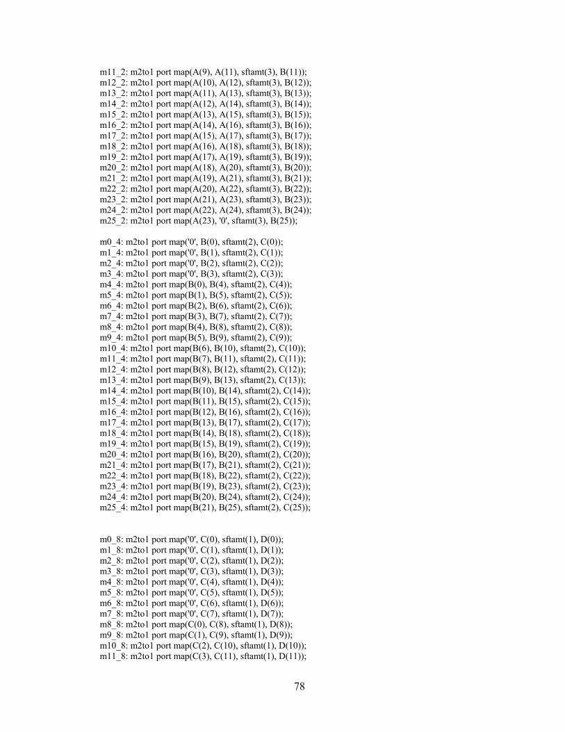
78
m11_2: m2to1 port map(A(9), A(11), sftamt(3), B(11)); m12_2: m2to1 port map(A(10), A(12), sftamt(3), B(12)); m13_2: m2to1 port map(A(11), A(13), sftamt(3), B(13)); m14_2: m2to1 port map(A(12), A(14), sftamt(3), B(14)); m15_2: m2to1 port map(A(13), A(15), sftamt(3), B(15)); m16_2: m2to1 port map(A(14), A(16), sftamt(3), B(16)); m17_2: m2to1 port map(A(15), A(17), sftamt(3), B(17)); m18_2: m2to1 port map(A(16), A(18), sftamt(3), B(18)); m19_2: m2to1 port map(A(17), A(19), sftamt(3), B(19)); m20_2: m2to1 port map(A(18), A(20), sftamt(3), B(20)); m21_2: m2to1 port map(A(19), A(21), sftamt(3), B(21)); m22_2: m2to1 port map(A(20), A(22), sftamt(3), B(22)); m23_2: m2to1 port map(A(21), A(23), sftamt(3), B(23)); m24_2: m2to1 port map(A(22), A(24), sftamt(3), B(24)); m25_2: m2to1 port map(A(23), '0', sftamt(3), B(25)); m0_4: m2to1 port map('0', B(0), sftamt(2), C(0)); m1_4: m2to1 port map('0', B(1), sftamt(2), C(1)); m2_4: m2to1 port map('0', B(2), sftamt(2), C(2)); m3_4: m2to1 port map('0', B(3), sftamt(2), C(3)); m4_4: m2to1 port map(B(0), B(4), sftamt(2), C(4)); m5_4: m2to1 port map(B(1), B(5), sftamt(2), C(5)); m6_4: m2to1 port map(B(2), B(6), sftamt(2), C(6)); m7_4: m2to1 port map(B(3), B(7), sftamt(2), C(7)); m8_4: m2to1 port map(B(4), B(8), sftamt(2), C(8)); m9_4: m2to1 port map(B(5), B(9), sftamt(2), C(9)); m10_4: m2to1 port map(B(6), B(10), sftamt(2), C(10)); m11_4: m2to1 port map(B(7), B(11), sftamt(2), C(11)); m12_4: m2to1 port map(B(8), B(12), sftamt(2), C(12)); m13_4: m2to1 port map(B(9), B(13), sftamt(2), C(13)); m14_4: m2to1 port map(B(10), B(14), sftamt(2), C(14)); m15_4: m2to1 port map(B(11), B(15), sftamt(2), C(15)); m16_4: m2to1 port map(B(12), B(16), sftamt(2), C(16)); m17_4: m2to1 port map(B(13), B(17), sftamt(2), C(17)); m18_4: m2to1 port map(B(14), B(18), sftamt(2), C(18)); m19_4: m2to1 port map(B(15), B(19), sftamt(2), C(19)); m20_4: m2to1 port map(B(16), B(20), sftamt(2), C(20)); m21_4: m2to1 port map(B(17), B(21), sftamt(2), C(21)); m22_4: m2to1 port map(B(18), B(22), sftamt(2), C(22)); m23_4: m2to1 port map(B(19), B(23), sftamt(2), C(23)); m24_4: m2to1 port map(B(20), B(24), sftamt(2), C(24)); m25_4: m2to1 port map(B(21), B(25), sftamt(2), C(25)); m0_8: m2to1 port map('0', C(0), sftamt(1), D(0)); m1_8: m2to1 port map('0', C(1), sftamt(1), D(1)); m2_8: m2to1 port map('0', C(2), sftamt(1), D(2)); m3_8: m2to1 port map('0', C(3), sftamt(1), D(3)); m4_8: m2to1 port map('0', C(4), sftamt(1), D(4)); m5_8: m2to1 port map('0', C(5), sftamt(1), D(5)); m6_8: m2to1 port map('0', C(6), sftamt(1), D(6)); m7_8: m2to1 port map('0', C(7), sftamt(1), D(7)); m8_8: m2to1 port map(C(0), C(8), sftamt(1), D(8)); m9_8: m2to1 port map(C(1), C(9), sftamt(1), D(9)); m10_8: m2to1 port map(C(2), C(10), sftamt(1), D(10)); m11_8: m2to1 port map(C(3), C(11), sftamt(1), D(11));
79
m12_8: m2to1 port map(C(4), C(12), sftamt(1), D(12)); m13_8: m2to1 port map(C(5), C(13), sftamt(1), D(13)); m14_8: m2to1 port map(C(6), C(14), sftamt(1), D(14)); m15_8: m2to1 port map(C(7), C(15), sftamt(1), D(15)); m16_8: m2to1 port map(C(8), C(16), sftamt(1), D(16)); m17_8: m2to1 port map(C(9), C(17), sftamt(1), D(17)); m18_8: m2to1 port map(C(10), C(18), sftamt(1), D(18)); m19_8: m2to1 port map(C(11), C(19), sftamt(1), D(19)); m20_8: m2to1 port map(C(12), C(20), sftamt(1), D(20)); m21_8: m2to1 port map(C(13), C(21), sftamt(1), D(21)); m22_8: m2to1 port map(C(14), C(22), sftamt(1), D(22)); m23_8: m2to1 port map(C(15), C(23), sftamt(1), D(23)); m24_8: m2to1 port map(C(16), C(24), sftamt(1), D(24)); m25_8: m2to1 port map(C(17), C(25), sftamt(1), D(25)); m0_16: m2to1 port map('0', D(0), sftamt(0), o(0)); m1_16: m2to1 port map('0', D(1), sftamt(0), o(1)); m2_16: m2to1 port map('0', D(2), sftamt(0), o(2)); m3_16: m2to1 port map('0', D(3), sftamt(0), o(3)); m4_16: m2to1 port map('0', D(4), sftamt(0), o(4)); m5_16: m2to1 port map('0', D(5), sftamt(0), o(5)); m6_16: m2to1 port map('0', D(6), sftamt(0), o(6)); m7_16: m2to1 port map('0', D(7), sftamt(0), o(7)); m8_16: m2to1 port map('0', D(8), sftamt(0), o(8)); m9_16: m2to1 port map('0', D(9), sftamt(0), o(9)); m10_16: m2to1 port map('0', D(10), sftamt(0), o(10)); m11_16: m2to1 port map('0', D(11), sftamt(0), o(11)); m12_16: m2to1 port map('0', D(12), sftamt(0), o(12)); m13_16: m2to1 port map('0', D(13), sftamt(0), o(13)); m14_16: m2to1 port map('0', D(14), sftamt(0), o(14)); m15_16: m2to1 port map('0', D(15), sftamt(0), o(15)); m16_16: m2to1 port map(D(0), D(16), sftamt(0), o(16)); m17_16: m2to1 port map(D(1), D(17), sftamt(0), o(17)); m18_16: m2to1 port map(D(2), D(18), sftamt(0), o(18)); m19_16: m2to1 port map(D(3), D(19), sftamt(0), o(19)); m20_16: m2to1 port map(D(4), D(20), sftamt(0), o(20)); m21_16: m2to1 port map(D(5), D(21), sftamt(0), o(21)); m22_16: m2to1 port map(D(6), D(22), sftamt(0), o(22)); m23_16: m2to1 port map(D(7), D(23), sftamt(0), o(23)); m24_16: m2to1 port map(D(8), D(24), sftamt(0), o(24)); m25_16: m2to1 port map(D(9), D(25), sftamt(0), o(25)); o(26)<= ((A(24) and sftamt(3)) or ((B(25) or B(24) or B(23) or B(22)) and sftamt(2)) or ((C(25) or C(24) or C(23) or C(22) or C(21) or C(20) or C(19) or C(18)) and sftamt(1)) or ((D(25) or D(24) or D(23) or D(22) or D(21) or D(20) or D(19) or D(18) or D(17) or D(16) or D(15) or D(14) or D(13) or D(12) or D(11) or D(10)) and sftamt(0))); end structure; 2:1 Multiplexer entity m2to1 is port( a0, b0, s: in std_logic; o: out std_logic); end m2to1;
80
architecture behaviour of m2to1 is begin o<=a0 when s='1' else b0; end behaviour; 2’s Complement Adder entity adder is port( a, b: in std_logic_vector(0 to 26); sub:in std_logic; sum: out std_logic_vector(0 to 26); cout: out std_logic); end adder; architecture equations of adder is signal x, y, invy, result: std_logic_vector(0 to 27); begin x<='0' & a; y<='0' & b; invy<= not y when sub='1' else y; result<= x + invy + ("00000000000000000000000000" & sub); cout<=result(0); sum<=result(1 to 27); end equations;
Leading One Detector entity lod is port ( f: in std_logic_vector(0 to 23); d: out std_logic_vector(0 to 4)); end lod; architecture equations of lod is component lod2 is port ( a, b: in std_logic; p: out std_logic; v: out std_logic); end component; component lod4 is port ( a, b, v0, v1: in std_logic; p: out std_logic_vector(0 to 1); v: out std_logic); end component; component lod8 is port ( a, b: in std_logic_vector(0 to 1); v0, v1: in std_logic;
81
p: out std_logic_vector(0 to 2); v: out std_logic); end component; component lod16 is port ( a, b: in std_logic_vector(0 to 2); v0, v1: in std_logic; p: out std_logic_vector(0 to 3); v: out std_logic); end component; component lod32 is port ( a, b: in std_logic_vector(0 to 3); v0, v1: in std_logic; p: out std_logic_vector(0 to 4); v: out std_logic); end component; signal p1, v1, p2: std_logic_vector(0 to 11); signal v2: std_logic_vector(0 to 5); signal p3: std_logic_vector(0 to 8); signal v3: std_logic_vector(0 to 2); signal p4: std_logic_vector(0 to 7); signal v4: std_logic_vector(0 to 1); signal p5: std_logic_vector(0 to 4); signal v5: std_logic; begin lod2_0: lod2 port map(f(0), f(1), p1(0), v1(0)); lod2_1: lod2 port map(f(2), f(3), p1(1), v1(1)); lod2_2: lod2 port map(f(4), f(5), p1(2), v1(2)); lod2_3: lod2 port map(f(6), f(7), p1(3), v1(3)); lod2_4: lod2 port map(f(8), f(9), p1(4), v1(4)); lod2_5: lod2 port map(f(10), f(11), p1(5), v1(5)); lod2_6: lod2 port map(f(12), f(13), p1(6), v1(6)); lod2_7: lod2 port map(f(14), f(15), p1(7), v1(7)); lod2_8: lod2 port map(f(16), f(17), p1(8), v1(8)); lod2_9: lod2 port map(f(18), f(19), p1(9), v1(9)); lod2_10: lod2 port map(f(20), f(21), p1(10), v1(10)); lod2_11: lod2 port map(f(22), f(23), p1(11), v1(11)); lod4_0: lod4 port map(p1(0), p1(1), v1(0), v1(1), p2( 0 to 1), v2(0)); lod4_1: lod4 port map(p1(2), p1(3), v1(2), v1(3), p2( 2 to 3), v2(1)); lod4_2: lod4 port map(p1(4), p1(5), v1(4), v1(5), p2( 4 to 5), v2(2)); lod4_3: lod4 port map(p1(6), p1(7), v1(6), v1(7), p2( 6 to 7), v2(3)); lod4_4: lod4 port map(p1(8), p1(9), v1(8), v1(9), p2( 8 to 9), v2(4)); lod4_5: lod4 port map(p1(10), p1(11), v1(10), v1(11), p2( 10 to 11), v2(5)); lod8_0: lod8 port map(p2(0 to 1), p2(2 to 3), v2(0), v2(1), p3(0 to 2), v3(0)); lod8_1: lod8 port map(p2(4 to 5), p2(6 to 7), v2(2), v2(3), p3(3 to 5), v3(1)); lod8_2: lod8 port map(p2(8 to 9), p2(10 to 11), v2(4), v2(5), p3(6 to 8), v3(2)); lod16_0: lod16 port map(p3(0 to 2), p3(3 to 5), v3(0), v3(1), p4(0 to 3), v4(0)); lod16_1: lod16 port map(p3(6 to 8), "000", v3(2), '0', p4(4 to 7), v4(1));
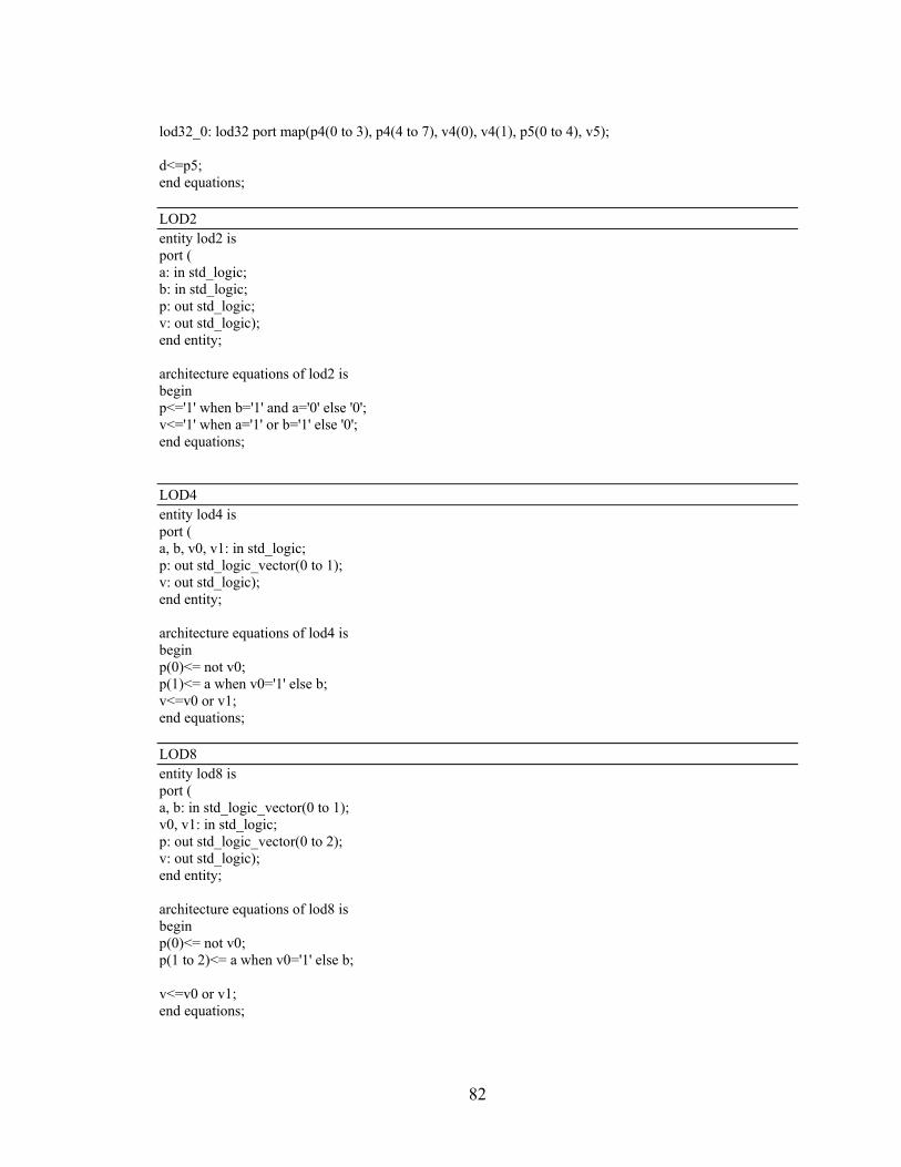
82
lod32_0: lod32 port map(p4(0 to 3), p4(4 to 7), v4(0), v4(1), p5(0 to 4), v5); d<=p5; end equations; LOD2 entity lod2 is port ( a: in std_logic; b: in std_logic; p: out std_logic; v: out std_logic); end entity; architecture equations of lod2 is begin p<='1' when b='1' and a='0' else '0'; v<='1' when a='1' or b='1' else '0'; end equations; LOD4 entity lod4 is port ( a, b, v0, v1: in std_logic; p: out std_logic_vector(0 to 1); v: out std_logic); end entity; architecture equations of lod4 is begin p(0)<= not v0; p(1)<= a when v0='1' else b; v<=v0 or v1; end equations; LOD8 entity lod8 is port ( a, b: in std_logic_vector(0 to 1); v0, v1: in std_logic; p: out std_logic_vector(0 to 2); v: out std_logic); end entity; architecture equations of lod8 is begin p(0)<= not v0; p(1 to 2)<= a when v0='1' else b; v<=v0 or v1; end equations;
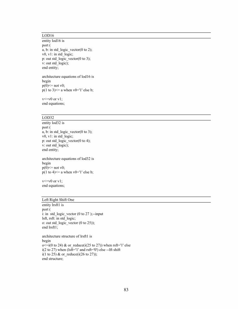
83
LOD16 entity lod16 is port ( a, b: in std_logic_vector(0 to 2); v0, v1: in std_logic; p: out std_logic_vector(0 to 3); v: out std_logic); end entity; architecture equations of lod16 is begin p(0)<= not v0; p(1 to 3)<= a when v0='1' else b; v<=v0 or v1; end equations; LOD32 entity lod32 is port ( a, b: in std_logic_vector(0 to 3); v0, v1: in std_logic; p: out std_logic_vector(0 to 4); v: out std_logic); end entity; architecture equations of lod32 is begin p(0)<= not v0; p(1 to 4)<= a when v0='1' else b; v<=v0 or v1; end equations; Left Right Shift One entity lrsft1 is port ( i: in std_logic_vector (0 to 27 );--input lsft, rsft: in std_logic; o: out std_logic_vector (0 to 25)); end lrsft1; architecture structure of lrsft1 is begin o<=i(0 to 24) & or_reduce(i(25 to 27)) when rsft='1' else i(2 to 27) when (lsft='1' and rsft='0') else --lft shift i(1 to 25) & or_reduce(i(26 to 27)); end structure;
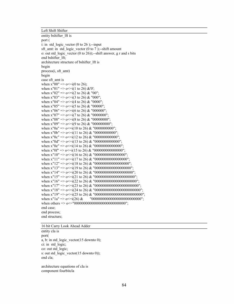
84
Left Shift Shifter entity bshifter_lft is port ( i: in std_logic_vector (0 to 26 );--input sft_amt: in std_logic_vector (0 to 7 );--shift amount o: out std_logic_vector (0 to 26));--shift answer, g r and s bits end bshifter_lft; architecture structure of bshifter_lft is begin process(i, sft_amt) begin case sft_amt is when x"00" => o<=i(0 to 26); when x"01" => o<=i(1 to 26) &'0'; when x"02" => o<=i(2 to 26) & "00"; when x"03" => o<=i(3 to 26) & "000"; when x"04" => o<=i(4 to 26) & "0000"; when x"05" => o<=i(5 to 26) & "00000"; when x"06" => o<=i(6 to 26) & "000000"; when x"07" => o<=i(7 to 26) & "0000000"; when x"08" => o<=i(8 to 26) & "00000000"; when x"09" => o<=i(9 to 26) & "000000000"; when x"0a" => o<=i(10 to 26) & "0000000000"; when x"0b" => o<=i(11 to 26) & "00000000000"; when x"0c" => o<=i(12 to 26) & "000000000000"; when x"0d" => o<=i(13 to 26) & "0000000000000"; when x"0e" => o<=i(14 to 26) & "00000000000000"; when x"0f" => o<=i(15 to 26) & "000000000000000"; when x"10" => o<=i(16 to 26) & "0000000000000000"; when x"11" => o<=i(17 to 26) & "00000000000000000"; when x"12" => o<=i(18 to 26) & "000000000000000000"; when x"13" => o<=i(19 to 26) & "0000000000000000000"; when x"14" => o<=i(20 to 26) & "00000000000000000000"; when x"15" => o<=i(21 to 26) & "000000000000000000000"; when x"16" => o<=i(22 to 26) & "0000000000000000000000"; when x"17" => o<=i(23 to 26) & "00000000000000000000000"; when x"18" => o<=i(24 to 26) & "000000000000000000000000"; when x"19" => o<=i(25 to 26) & "0000000000000000000000000"; when x"1a" => o<=i(26) & "00000000000000000000000000"; when others => o<="000000000000000000000000000"; end case; end process; end structure; 16 bit Carry Look Ahead Adder entity cla is port( a, b: in std_logic_vector(15 downto 0); ci: in std_logic; co: out std_logic; s: out std_logic_vector(15 downto 0)); end cla; architecture equations of cla is component fourbitcla
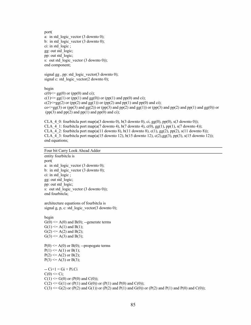
85
port( a: in std_logic_vector (3 downto 0); b: in std_logic_vector (3 downto 0); ci: in std_logic ; gg: out std_logic; pp: out std_logic; s: out std_logic_vector (3 downto 0)); end component; signal gg , pp: std_logic_vector(3 downto 0); signal c: std_logic_vector(2 downto 0); begin c(0)<= gg(0) or (pp(0) and ci); c(1)<= gg(1) or (pp(1) and gg(0)) or (pp(1) and pp(0) and ci); c(2)<=gg(2) or (pp(2) and gg(1)) or (pp(2) and pp(1) and pp(0) and ci); co<=gg(3) or (pp(3) and gg(2)) or (pp(3) and pp(2) and gg(1)) or (pp(3) and pp(2) and pp(1) and gg(0)) or (pp(3) and pp(2) and pp(1) and pp(0) and ci); CLA_4_0: fourbitcla port map(a(3 downto 0), b(3 downto 0), ci, gg(0), pp(0), s(3 downto 0)); CLA_4_1: fourbitcla port map(a(7 downto 4), b(7 downto 4), c(0), gg(1), pp(1), s(7 downto 4)); CLA_4_2: fourbitcla port map(a(11 downto 8), b(11 downto 8), c(1), gg(2), pp(2), s(11 downto 8)); CLA_4_3: fourbitcla port map(a(15 downto 12), b(15 downto 12), c(2),gg(3), pp(3), s(15 downto 12)); end equations; Four bit Carry Look Ahead Adder entity fourbitcla is port( a: in std_logic_vector (3 downto 0); b: in std_logic_vector (3 downto 0); ci: in std_logic ; gg: out std_logic; pp: out std_logic; s: out std_logic_vector (3 downto 0)); end fourbitcla; architecture equations of fourbitcla is signal g, p, c: std_logic_vector(3 downto 0); begin G(0) <= A(0) and B(0); --generate terms G(1) <= A(1) and B(1); G(2) <= A(2) and B(2); G(3) <= A(3) and B(3); P(0) <= A(0) or B(0); --propogate terms P(1) <= A(1) or B(1); P(2) <= A(2) or B(2); P(3) <= A(3) or B(3); -- Ci+1 = Gi + Pi.Ci C(0) <= Ci; C(1) <= G(0) or (P(0) and C(0)); C(2) <= G(1) or (P(1) and G(0)) or (P(1) and P(0) and C(0)); C(3) <= G(2) or (P(2) and G(1)) or (P(2) and P(1) and G(0)) or (P(2) and P(1) and P(0) and C(0));
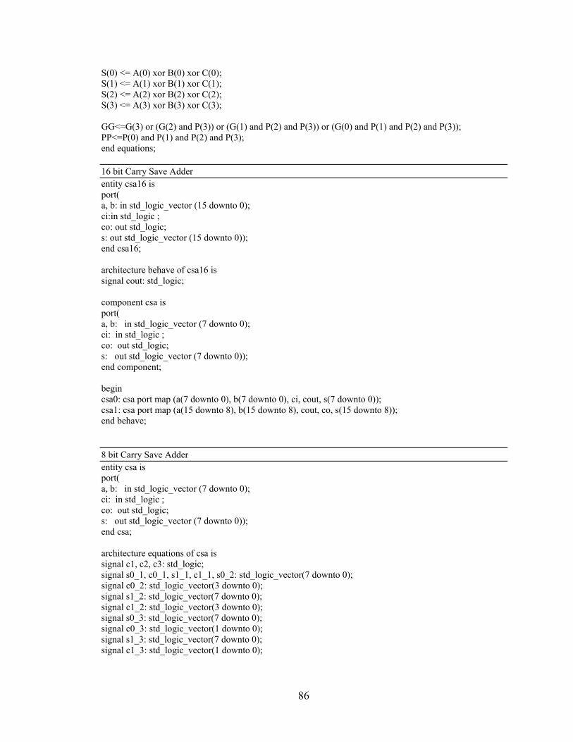
86
S(0) <= A(0) xor B(0) xor C(0); S(1) <= A(1) xor B(1) xor C(1); S(2) <= A(2) xor B(2) xor C(2); S(3) <= A(3) xor B(3) xor C(3); GG<=G(3) or (G(2) and P(3)) or (G(1) and P(2) and P(3)) or (G(0) and P(1) and P(2) and P(3)); PP<=P(0) and P(1) and P(2) and P(3); end equations; 16 bit Carry Save Adder entity csa16 is port( a, b: in std_logic_vector (15 downto 0); ci:in std_logic ; co: out std_logic; s: out std_logic_vector (15 downto 0)); end csa16; architecture behave of csa16 is signal cout: std_logic; component csa is port( a, b: in std_logic_vector (7 downto 0); ci: in std_logic ; co: out std_logic; s: out std_logic_vector (7 downto 0)); end component; begin csa0: csa port map (a(7 downto 0), b(7 downto 0), ci, cout, s(7 downto 0)); csa1: csa port map (a(15 downto 8), b(15 downto 8), cout, co, s(15 downto 8)); end behave; 8 bit Carry Save Adder entity csa is port( a, b: in std_logic_vector (7 downto 0); ci: in std_logic ; co: out std_logic; s: out std_logic_vector (7 downto 0)); end csa; architecture equations of csa is signal c1, c2, c3: std_logic; signal s0_1, c0_1, s1_1, c1_1, s0_2: std_logic_vector(7 downto 0); signal c0_2: std_logic_vector(3 downto 0); signal s1_2: std_logic_vector(7 downto 0); signal c1_2: std_logic_vector(3 downto 0); signal s0_3: std_logic_vector(7 downto 0); signal c0_3: std_logic_vector(1 downto 0); signal s1_3: std_logic_vector(7 downto 0); signal c1_3: std_logic_vector(1 downto 0);
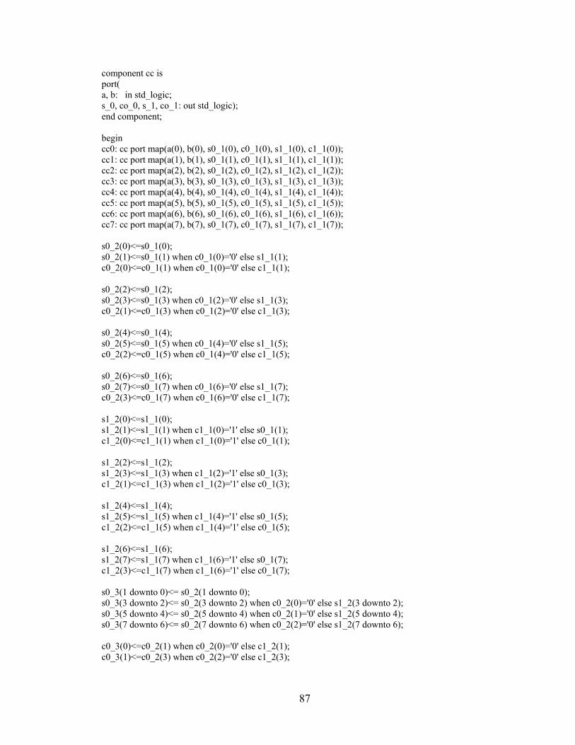
87
component cc is port( a, b: in std_logic; s_0, co_0, s_1, co_1: out std_logic); end component; begin cc0: cc port map(a(0), b(0), s0_1(0), c0_1(0), s1_1(0), c1_1(0)); cc1: cc port map(a(1), b(1), s0_1(1), c0_1(1), s1_1(1), c1_1(1)); cc2: cc port map(a(2), b(2), s0_1(2), c0_1(2), s1_1(2), c1_1(2)); cc3: cc port map(a(3), b(3), s0_1(3), c0_1(3), s1_1(3), c1_1(3)); cc4: cc port map(a(4), b(4), s0_1(4), c0_1(4), s1_1(4), c1_1(4)); cc5: cc port map(a(5), b(5), s0_1(5), c0_1(5), s1_1(5), c1_1(5)); cc6: cc port map(a(6), b(6), s0_1(6), c0_1(6), s1_1(6), c1_1(6)); cc7: cc port map(a(7), b(7), s0_1(7), c0_1(7), s1_1(7), c1_1(7)); s0_2(0)<=s0_1(0); s0_2(1)<=s0_1(1) when c0_1(0)='0' else s1_1(1); c0_2(0)<=c0_1(1) when c0_1(0)='0' else c1_1(1); s0_2(2)<=s0_1(2); s0_2(3)<=s0_1(3) when c0_1(2)='0' else s1_1(3); c0_2(1)<=c0_1(3) when c0_1(2)='0' else c1_1(3); s0_2(4)<=s0_1(4); s0_2(5)<=s0_1(5) when c0_1(4)='0' else s1_1(5); c0_2(2)<=c0_1(5) when c0_1(4)='0' else c1_1(5); s0_2(6)<=s0_1(6); s0_2(7)<=s0_1(7) when c0_1(6)='0' else s1_1(7); c0_2(3)<=c0_1(7) when c0_1(6)='0' else c1_1(7); s1_2(0)<=s1_1(0); s1_2(1)<=s1_1(1) when c1_1(0)='1' else s0_1(1); c1_2(0)<=c1_1(1) when c1_1(0)='1' else c0_1(1); s1_2(2)<=s1_1(2); s1_2(3)<=s1_1(3) when c1_1(2)='1' else s0_1(3); c1_2(1)<=c1_1(3) when c1_1(2)='1' else c0_1(3); s1_2(4)<=s1_1(4); s1_2(5)<=s1_1(5) when c1_1(4)='1' else s0_1(5); c1_2(2)<=c1_1(5) when c1_1(4)='1' else c0_1(5); s1_2(6)<=s1_1(6); s1_2(7)<=s1_1(7) when c1_1(6)='1' else s0_1(7); c1_2(3)<=c1_1(7) when c1_1(6)='1' else c0_1(7); s0_3(1 downto 0)<= s0_2(1 downto 0); s0_3(3 downto 2)<= s0_2(3 downto 2) when c0_2(0)='0' else s1_2(3 downto 2); s0_3(5 downto 4)<= s0_2(5 downto 4) when c0_2(1)='0' else s1_2(5 downto 4); s0_3(7 downto 6)<= s0_2(7 downto 6) when c0_2(2)='0' else s1_2(7 downto 6); c0_3(0)<=c0_2(1) when c0_2(0)='0' else c1_2(1); c0_3(1)<=c0_2(3) when c0_2(2)='0' else c1_2(3);
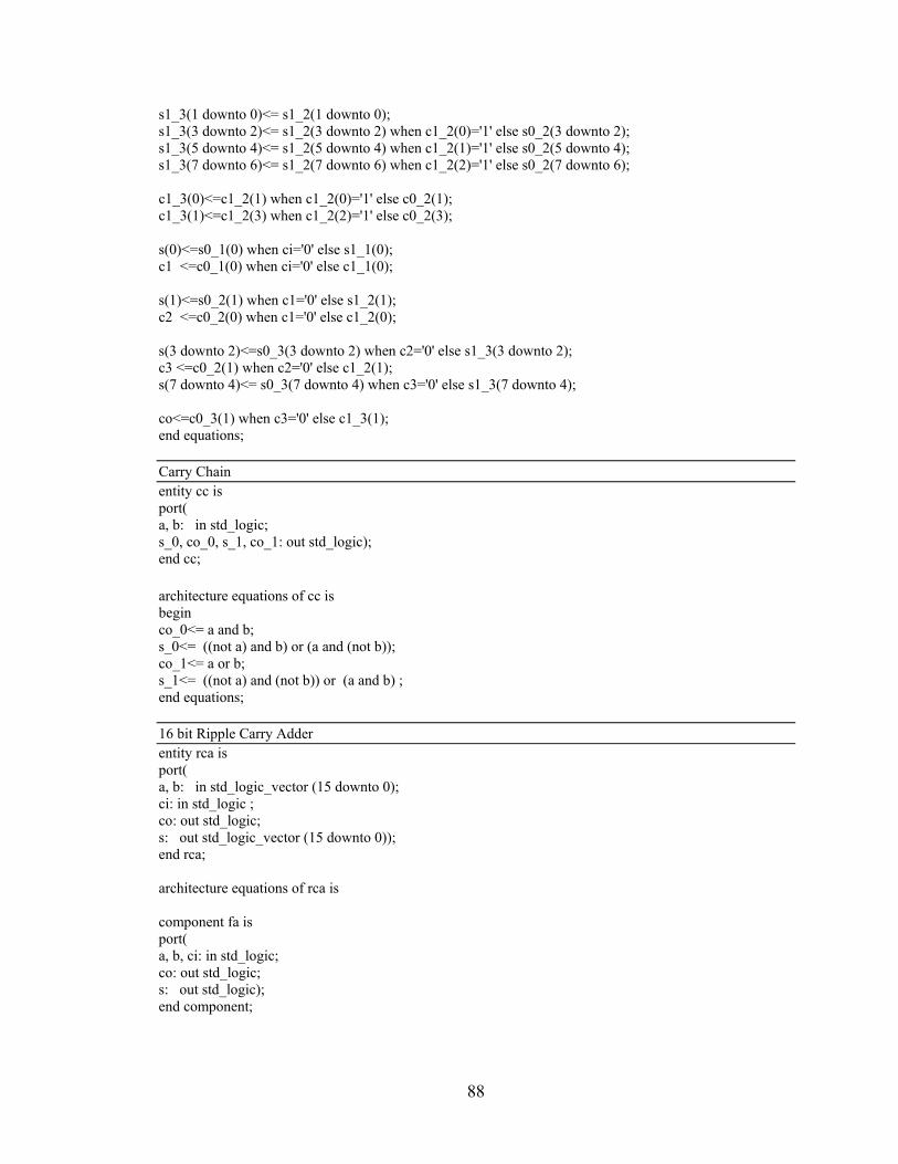
88
s1_3(1 downto 0)<= s1_2(1 downto 0); s1_3(3 downto 2)<= s1_2(3 downto 2) when c1_2(0)='1' else s0_2(3 downto 2); s1_3(5 downto 4)<= s1_2(5 downto 4) when c1_2(1)='1' else s0_2(5 downto 4); s1_3(7 downto 6)<= s1_2(7 downto 6) when c1_2(2)='1' else s0_2(7 downto 6); c1_3(0)<=c1_2(1) when c1_2(0)='1' else c0_2(1); c1_3(1)<=c1_2(3) when c1_2(2)='1' else c0_2(3); s(0)<=s0_1(0) when ci='0' else s1_1(0); c1 <=c0_1(0) when ci='0' else c1_1(0); s(1)<=s0_2(1) when c1='0' else s1_2(1); c2 <=c0_2(0) when c1='0' else c1_2(0); s(3 downto 2)<=s0_3(3 downto 2) when c2='0' else s1_3(3 downto 2); c3 <=c0_2(1) when c2='0' else c1_2(1); s(7 downto 4)<= s0_3(7 downto 4) when c3='0' else s1_3(7 downto 4); co<=c0_3(1) when c3='0' else c1_3(1); end equations; Carry Chain entity cc is port( a, b: in std_logic; s_0, co_0, s_1, co_1: out std_logic); end cc; architecture equations of cc is begin co_0<= a and b; s_0<= ((not a) and b) or (a and (not b)); co_1<= a or b; s_1<= ((not a) and (not b)) or (a and b) ; end equations; 16 bit Ripple Carry Adder entity rca is port( a, b: in std_logic_vector (15 downto 0); ci: in std_logic ; co: out std_logic; s: out std_logic_vector (15 downto 0)); end rca; architecture equations of rca is component fa is port( a, b, ci: in std_logic; co: out std_logic; s: out std_logic); end component;
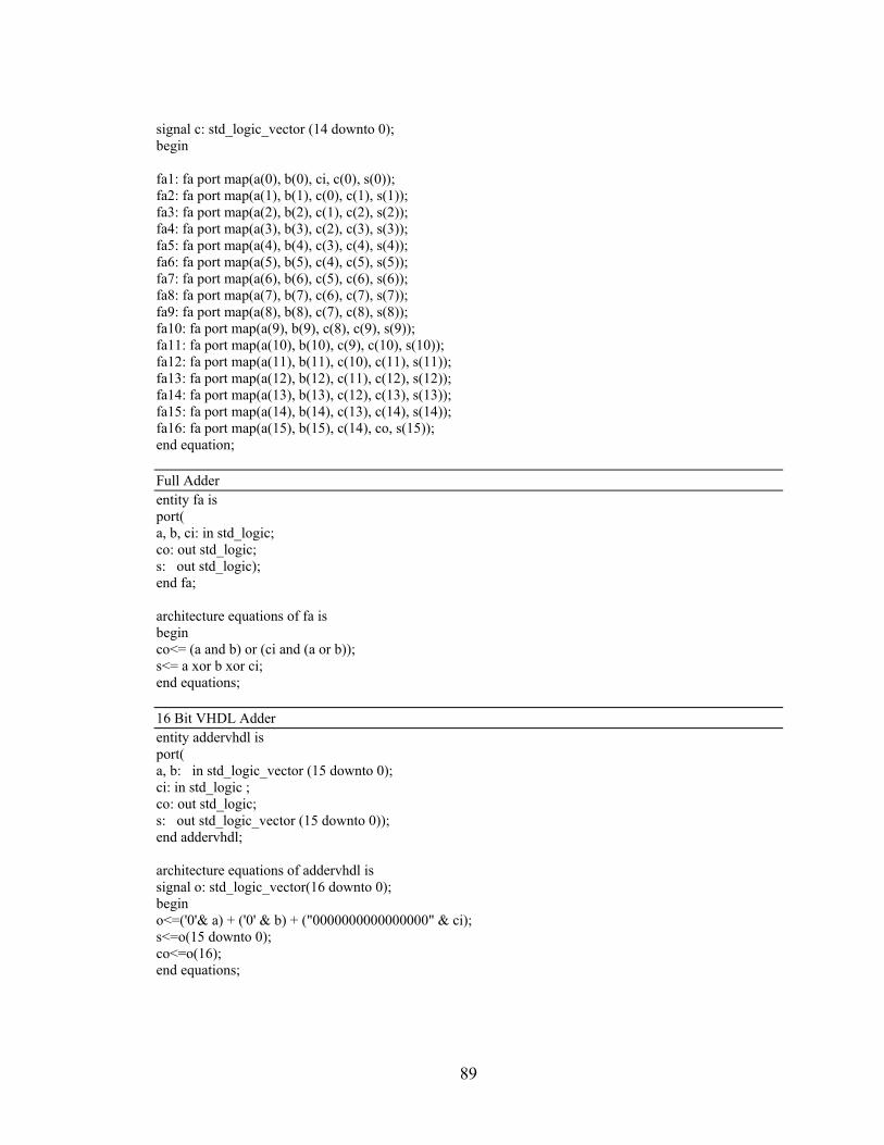
89
signal c: std_logic_vector (14 downto 0); begin fa1: fa port map(a(0), b(0), ci, c(0), s(0)); fa2: fa port map(a(1), b(1), c(0), c(1), s(1)); fa3: fa port map(a(2), b(2), c(1), c(2), s(2)); fa4: fa port map(a(3), b(3), c(2), c(3), s(3)); fa5: fa port map(a(4), b(4), c(3), c(4), s(4)); fa6: fa port map(a(5), b(5), c(4), c(5), s(5)); fa7: fa port map(a(6), b(6), c(5), c(6), s(6)); fa8: fa port map(a(7), b(7), c(6), c(7), s(7)); fa9: fa port map(a(8), b(8), c(7), c(8), s(8)); fa10: fa port map(a(9), b(9), c(8), c(9), s(9)); fa11: fa port map(a(10), b(10), c(9), c(10), s(10)); fa12: fa port map(a(11), b(11), c(10), c(11), s(11)); fa13: fa port map(a(12), b(12), c(11), c(12), s(12)); fa14: fa port map(a(13), b(13), c(12), c(13), s(13)); fa15: fa port map(a(14), b(14), c(13), c(14), s(14)); fa16: fa port map(a(15), b(15), c(14), co, s(15)); end equation; Full Adder entity fa is port( a, b, ci: in std_logic; co: out std_logic; s: out std_logic); end fa; architecture equations of fa is begin co<= (a and b) or (ci and (a or b)); s<= a xor b xor ci; end equations; 16 Bit VHDL Adder entity addervhdl is port( a, b: in std_logic_vector (15 downto 0); ci: in std_logic ; co: out std_logic; s: out std_logic_vector (15 downto 0)); end addervhdl; architecture equations of addervhdl is signal o: std_logic_vector(16 downto 0); begin o<=('0'& a) + ('0' & b) + ("0000000000000000" & ci); s<=o(15 downto 0); co<=o(16); end equations;
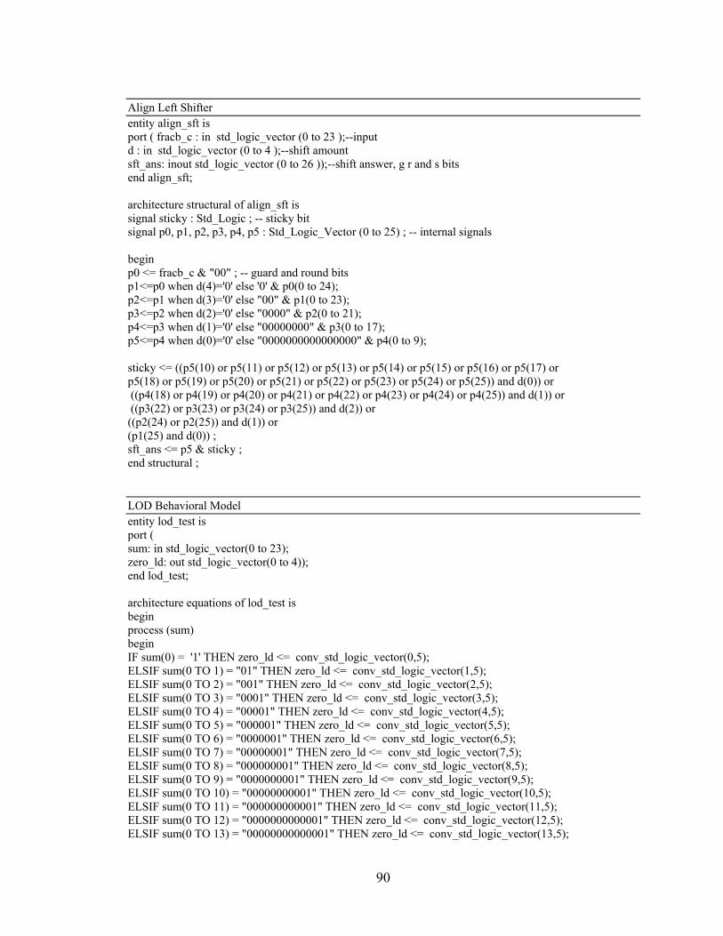
90
Align Left Shifter entity align_sft is port ( fracb_c : in std_logic_vector (0 to 23 );--input d : in std_logic_vector (0 to 4 );--shift amount sft_ans: inout std_logic_vector (0 to 26 ));--shift answer, g r and s bits end align_sft; architecture structural of align_sft is signal sticky : Std_Logic ; -- sticky bit signal p0, p1, p2, p3, p4, p5 : Std_Logic_Vector (0 to 25) ; -- internal signals begin p0 <= fracb_c & "00" ; -- guard and round bits p1<=p0 when d(4)='0' else '0' & p0(0 to 24); p2<=p1 when d(3)='0' else "00" & p1(0 to 23); p3<=p2 when d(2)='0' else "0000" & p2(0 to 21); p4<=p3 when d(1)='0' else "00000000" & p3(0 to 17); p5<=p4 when d(0)='0' else "0000000000000000" & p4(0 to 9); sticky <= ((p5(10) or p5(11) or p5(12) or p5(13) or p5(14) or p5(15) or p5(16) or p5(17) or p5(18) or p5(19) or p5(20) or p5(21) or p5(22) or p5(23) or p5(24) or p5(25)) and d(0)) or ((p4(18) or p4(19) or p4(20) or p4(21) or p4(22) or p4(23) or p4(24) or p4(25)) and d(1)) or ((p3(22) or p3(23) or p3(24) or p3(25)) and d(2)) or ((p2(24) or p2(25)) and d(1)) or (p1(25) and d(0)) ; sft_ans <= p5 & sticky ; end structural ; LOD Behavioral Model entity lod_test is port ( sum: in std_logic_vector(0 to 23); zero_ld: out std_logic_vector(0 to 4)); end lod_test; architecture equations of lod_test is begin process (sum) begin IF sum(0) = '1' THEN zero_ld <= conv_std_logic_vector(0,5); ELSIF sum(0 TO 1) = "01" THEN zero_ld <= conv_std_logic_vector(1,5); ELSIF sum(0 TO 2) = "001" THEN zero_ld <= conv_std_logic_vector(2,5); ELSIF sum(0 TO 3) = "0001" THEN zero_ld <= conv_std_logic_vector(3,5); ELSIF sum(0 TO 4) = "00001" THEN zero_ld <= conv_std_logic_vector(4,5); ELSIF sum(0 TO 5) = "000001" THEN zero_ld <= conv_std_logic_vector(5,5); ELSIF sum(0 TO 6) = "0000001" THEN zero_ld <= conv_std_logic_vector(6,5); ELSIF sum(0 TO 7) = "00000001" THEN zero_ld <= conv_std_logic_vector(7,5); ELSIF sum(0 TO 8) = "000000001" THEN zero_ld <= conv_std_logic_vector(8,5); ELSIF sum(0 TO 9) = "0000000001" THEN zero_ld <= conv_std_logic_vector(9,5); ELSIF sum(0 TO 10) = "00000000001" THEN zero_ld <= conv_std_logic_vector(10,5); ELSIF sum(0 TO 11) = "000000000001" THEN zero_ld <= conv_std_logic_vector(11,5); ELSIF sum(0 TO 12) = "0000000000001" THEN zero_ld <= conv_std_logic_vector(12,5); ELSIF sum(0 TO 13) = "00000000000001" THEN zero_ld <= conv_std_logic_vector(13,5);
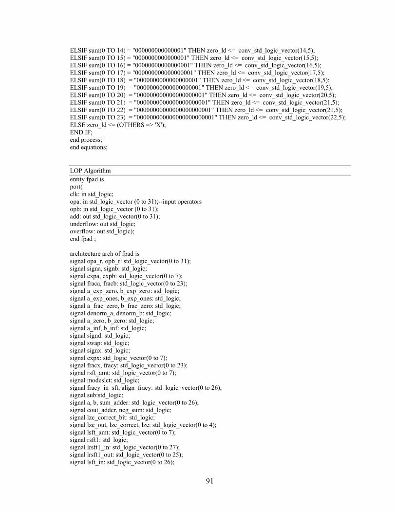
91
ELSIF sum(0 TO 14) = "000000000000001" THEN zero_ld <= conv_std_logic_vector(14,5); ELSIF sum(0 TO 15) = "0000000000000001" THEN zero_ld <= conv_std_logic_vector(15,5); ELSIF sum(0 TO 16) = "00000000000000001" THEN zero_ld <= conv_std_logic_vector(16,5); ELSIF sum(0 TO 17) = "000000000000000001" THEN zero_ld <= conv_std_logic_vector(17,5); ELSIF sum(0 TO 18) = "0000000000000000001" THEN zero_ld <= conv_std_logic_vector(18,5); ELSIF sum(0 TO 19) = "00000000000000000001" THEN zero_ld <= conv_std_logic_vector(19,5); ELSIF sum(0 TO 20) = "000000000000000000001" THEN zero_ld <= conv_std_logic_vector(20,5); ELSIF sum(0 TO 21) = "0000000000000000000001" THEN zero_ld <= conv_std_logic_vector(21,5); ELSIF sum(0 TO 22) = "00000000000000000000001" THEN zero_ld <= conv_std_logic_vector(21,5); ELSIF sum(0 TO 23) = "000000000000000000000001" THEN zero_ld <= conv_std_logic_vector(22,5); ELSE zero_ld <= (OTHERS => 'X'); END IF; end process; end equations; LOP Algorithm entity fpad is port( clk: in std_logic; opa: in std_logic_vector (0 to 31);--input operators opb: in std_logic_vector (0 to 31); add: out std_logic_vector(0 to 31); underflow: out std_logic; overflow: out std_logic); end fpad ; architecture arch of fpad is signal opa_r, opb_r: std_logic_vector(0 to 31); signal signa, signb: std_logic; signal expa, expb: std_logic_vector(0 to 7); signal fraca, fracb: std_logic_vector(0 to 23); signal a_exp_zero, b_exp_zero: std_logic; signal a_exp_ones, b_exp_ones: std_logic; signal a_frac_zero, b_frac_zero: std_logic; signal denorm_a, denorm_b: std_logic; signal a_zero, b_zero: std_logic; signal a_inf, b_inf: std_logic; signal signd: std_logic; signal swap: std_logic; signal signx: std_logic; signal expx: std_logic_vector(0 to 7); signal fracx, fracy: std_logic_vector(0 to 23); signal rsft_amt: std_logic_vector(0 to 7); signal modeslct: std_logic; signal fracy_in_sft, align_fracy: std_logic_vector(0 to 26); signal sub:std_logic; signal a, b, sum_adder: std_logic_vector(0 to 26); signal cout_adder, neg_sum: std_logic; signal lzc_correct_bit: std_logic; signal lzc_out, lzc_correct, lzc: std_logic_vector(0 to 4); signal lsft_amt: std_logic_vector(0 to 7); signal rsft1: std_logic; signal lrsft1_in: std_logic_vector(0 to 27); signal lrsft1_out: std_logic_vector(0 to 25); signal lsft_in: std_logic_vector(0 to 26);
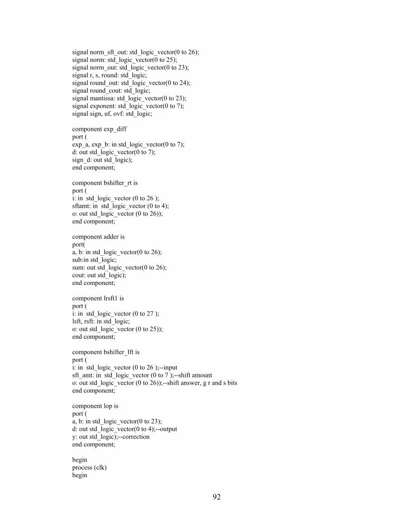
92
signal norm_sft_out: std_logic_vector(0 to 26); signal norm: std_logic_vector(0 to 25); signal norm_out: std_logic_vector(0 to 23); signal r, s, round: std_logic; signal round_out: std_logic_vector(0 to 24); signal round_cout: std_logic; signal mantissa: std_logic_vector(0 to 23); signal exponent: std_logic_vector(0 to 7); signal sign, uf, ovf: std_logic; component exp_diff port ( exp_a, exp_b: in std_logic_vector(0 to 7); d: out std_logic_vector(0 to 7); sign_d: out std_logic); end component; component bshifter_rt is port ( i: in std_logic_vector (0 to 26 ); sftamt: in std_logic_vector (0 to 4); o: out std_logic_vector (0 to 26)); end component; component adder is port( a, b: in std_logic_vector(0 to 26); sub:in std_logic; sum: out std_logic_vector(0 to 26); cout: out std_logic); end component; component lrsft1 is port ( i: in std_logic_vector (0 to 27 ); lsft, rsft: in std_logic; o: out std_logic_vector (0 to 25)); end component; component bshifter_lft is port ( i: in std_logic_vector (0 to 26 );--input sft_amt: in std_logic_vector (0 to 7 );--shift amount o: out std_logic_vector (0 to 26));--shift answer, g r and s bits end component; component lop is port ( a, b: in std_logic_vector(0 to 23); d: out std_logic_vector(0 to 4);--output y: out std_logic);--correction end component; begin process (clk) begin
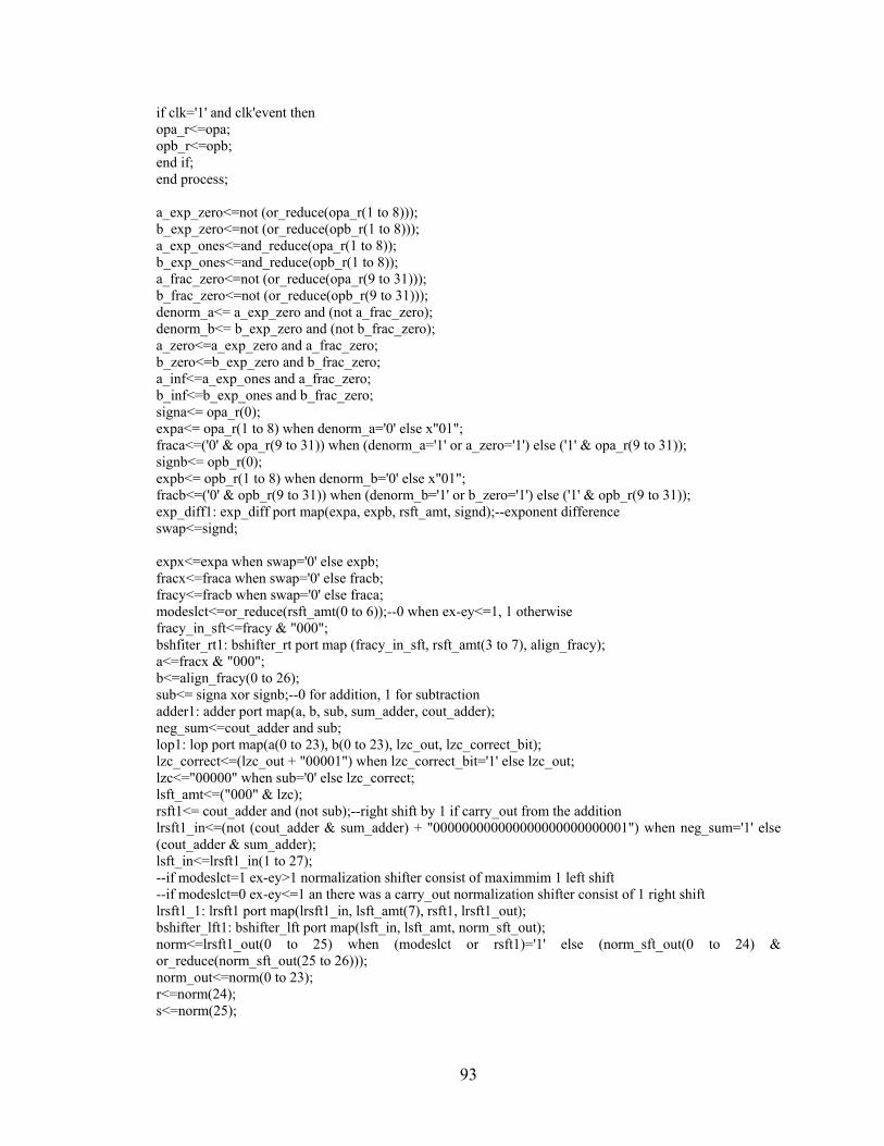
93
if clk='1' and clk'event then opa_r<=opa; opb_r<=opb; end if; end process; a_exp_zero<=not (or_reduce(opa_r(1 to 8))); b_exp_zero<=not (or_reduce(opb_r(1 to 8))); a_exp_ones<=and_reduce(opa_r(1 to 8)); b_exp_ones<=and_reduce(opb_r(1 to 8)); a_frac_zero<=not (or_reduce(opa_r(9 to 31))); b_frac_zero<=not (or_reduce(opb_r(9 to 31))); denorm_a<= a_exp_zero and (not a_frac_zero); denorm_b<= b_exp_zero and (not b_frac_zero); a_zero<=a_exp_zero and a_frac_zero; b_zero<=b_exp_zero and b_frac_zero; a_inf<=a_exp_ones and a_frac_zero; b_inf<=b_exp_ones and b_frac_zero; signa<= opa_r(0); expa<= opa_r(1 to 8) when denorm_a='0' else x"01"; fraca<=('0' & opa_r(9 to 31)) when (denorm_a='1' or a_zero='1') else ('1' & opa_r(9 to 31)); signb<= opb_r(0); expb<= opb_r(1 to 8) when denorm_b='0' else x"01"; fracb<=('0' & opb_r(9 to 31)) when (denorm_b='1' or b_zero='1') else ('1' & opb_r(9 to 31)); exp_diff1: exp_diff port map(expa, expb, rsft_amt, signd);--exponent difference swap<=signd; expx<=expa when swap='0' else expb; fracx<=fraca when swap='0' else fracb; fracy<=fracb when swap='0' else fraca; modeslct<=or_reduce(rsft_amt(0 to 6));--0 when ex-ey<=1, 1 otherwise fracy_in_sft<=fracy & "000"; bshfiter_rt1: bshifter_rt port map (fracy_in_sft, rsft_amt(3 to 7), align_fracy); a<=fracx & "000"; b<=align_fracy(0 to 26); sub<= signa xor signb;--0 for addition, 1 for subtraction adder1: adder port map(a, b, sub, sum_adder, cout_adder); neg_sum<=cout_adder and sub; lop1: lop port map(a(0 to 23), b(0 to 23), lzc_out, lzc_correct_bit); lzc_correct<=(lzc_out + "00001") when lzc_correct_bit='1' else lzc_out; lzc<="00000" when sub='0' else lzc_correct; lsft_amt<=("000" & lzc); rsft1<= cout_adder and (not sub);--right shift by 1 if carry_out from the addition lrsft1_in<=(not (cout_adder & sum_adder) + "000000000000000000000000001") when neg_sum='1' else (cout_adder & sum_adder); lsft_in<=lrsft1_in(1 to 27); --if modeslct=1 ex-ey>1 normalization shifter consist of maximmim 1 left shift --if modeslct=0 ex-ey<=1 an there was a carry_out normalization shifter consist of 1 right shift lrsft1_1: lrsft1 port map(lrsft1_in, lsft_amt(7), rsft1, lrsft1_out); bshifter_lft1: bshifter_lft port map(lsft_in, lsft_amt, norm_sft_out); norm<=lrsft1_out(0 to 25) when (modeslct or rsft1)='1' else (norm_sft_out(0 to 24) & or_reduce(norm_sft_out(25 to 26))); norm_out<=norm(0 to 23); r<=norm(24); s<=norm(25);
94
round<=(r and s) or (r and norm_out(23)); round_out<=(('0' & norm_out) + "0000000000000000000000001") when round='1' else ('0' & norm_out); round_cout<=round_out(0); mantissa<=(round_cout & round_out(1 to 23)) when round_cout='1' else round_out(1 to 24); exponent<=(expx + x"01") when (rsft1 or round_cout)='1' else (expx - lsft_amt); uf<='1' when exponent=x"01" and mantissa(0)='0' else '0'; ovf<='1' when exponent=x"FF" or a_inf='1' or b_inf='1' else '0'; signx<=signb when swap='1' or neg_sum='1' else signa; sign<=signx; process (clk) begin if clk='1' and clk'event then add<=sign & exponent & mantissa(1 to 23); underflow<=uf; overflow<=ovf; end if; end process; end arch; 5 Stages Pipeline LOP Algorithm entity fpad_p is port( clk: in std_logic; opa: in std_logic_vector (0 to 31);--input operators opb: in std_logic_vector (0 to 31); add: out std_logic_vector(0 to 31); underflow: out std_logic; overflow: out std_logic); end fpad_p ; architecture arch of fpad_p is signal opa_r, opb_r: std_logic_vector(0 to 31); signal signa_r, signb_r, swap_r, a_inf_r, b_inf_r: std_logic; signal expx_r: std_logic_vector(0 to 7); signal fracy_in_sft_r: std_logic_vector(0 to 26); signal rsft_amt_r: std_logic_vector(0 to 7); signal fracx_r: std_logic_vector(0 to 23); signal signa_r_r, signb_r_r, modeslct_r, swap_r_r, sub_r, a_inf_r_r, b_inf_r_r: std_logic; signal a_r, b_r: std_logic_vector(0 to 26); signal expx_r_r: std_logic_vector(0 to 7); signal lrsft1_in_r: std_logic_vector(0 to 27); signal lsft_amt_r: std_logic_vector(0 to 7); signal rsft1_r, sign_r, modeslct_r_r, a_inf_r_r_r, b_inf_r_r_r: std_logic; signal expx_r_r_r: std_logic_vector(0 to 7); signal round_r: std_logic; signal norm_out_r: std_logic_vector(0 to 23); signal lsft_amt_r_r: std_logic_vector(0 to 7); signal rsft1_r_r, sign_r_r, a_inf_r_r_r_r, b_inf_r_r_r_r: std_logic; signal expx_r_r_r_r: std_logic_vector(0 to 7); signal signa, signb: std_logic; signal expa, expb: std_logic_vector(0 to 7); signal fraca, fracb: std_logic_vector(0 to 23);
95
signal a_exp_zero, b_exp_zero: std_logic; signal a_exp_ones, b_exp_ones: std_logic; signal a_frac_zero, b_frac_zero: std_logic; signal denorm_a, denorm_b: std_logic; signal a_zero, b_zero: std_logic; signal a_inf, b_inf: std_logic; signal signd: std_logic; signal swap: std_logic; signal expx: std_logic_vector(0 to 7); signal fracx, fracy: std_logic_vector(0 to 23); signal rsft_amt: std_logic_vector(0 to 7); signal modeslct: std_logic; signal fracy_in_sft, align_fracy: std_logic_vector(0 to 26); signal a, b: std_logic_vector(0 to 26); signal sub:std_logic; signal sum_adder: std_logic_vector(0 to 26); signal cout_adder, neg_sum: std_logic; signal lzc_correct_bit: std_logic; signal lzc_out, lzc_correct, lzc: std_logic_vector(0 to 4); signal lsft_amt: std_logic_vector(0 to 7); signal rsft1: std_logic; signal lrsft1_in: std_logic_vector(0 to 27); signal signx: std_logic; signal sign: std_logic; signal lrsft1_out: std_logic_vector(0 to 25); signal norm_sft_out: std_logic_vector(0 to 26); signal norm: std_logic_vector(0 to 25); signal norm_out: std_logic_vector(0 to 23); signal r, s, round: std_logic; signal round_out: std_logic_vector(0 to 24); signal round_cout: std_logic; signal mantissa: std_logic_vector(0 to 23); signal exponent: std_logic_vector(0 to 7); signal uf, ovf: std_logic; component exp_diff port ( exp_a, exp_b: in std_logic_vector(0 to 7); d: out std_logic_vector(0 to 7); sign_d: out std_logic); end component; component bshifter_rt is port ( i: in std_logic_vector (0 to 26 ); sftamt: in std_logic_vector (0 to 4); o: out std_logic_vector (0 to 26)); end component; component adder is port( a, b: in std_logic_vector(0 to 26); sub:in std_logic; sum: out std_logic_vector(0 to 26); cout: out std_logic); end component;
96
component lrsft1 is port ( i: in std_logic_vector (0 to 27 ); lsft, rsft: in std_logic; o: out std_logic_vector (0 to 25)); end component; component bshifter_lft is port ( i: in std_logic_vector (0 to 26 );--input sft_amt: in std_logic_vector (0 to 7 );--shift amount o: out std_logic_vector (0 to 26));--shift answer, g r and s bits end component; component lop is port ( a, b: in std_logic_vector(0 to 23); d: out std_logic_vector(0 to 4);--output y: out std_logic);--correction end component; begin process (clk) begin if clk='1' and clk'event then opa_r<=opa; opb_r<=opb; end if; end process; a_exp_zero<=not (or_reduce(opa_r(1 to 8))); b_exp_zero<=not (or_reduce(opb_r(1 to 8))); a_exp_ones<=and_reduce(opa_r(1 to 8)); b_exp_ones<=and_reduce(opb_r(1 to 8)); a_frac_zero<=not (or_reduce(opa_r(9 to 31))); b_frac_zero<=not (or_reduce(opb_r(9 to 31))); denorm_a<= a_exp_zero and (not a_frac_zero); denorm_b<= b_exp_zero and (not b_frac_zero); a_zero<=a_exp_zero and a_frac_zero; b_zero<=b_exp_zero and b_frac_zero; a_inf<=a_exp_ones and a_frac_zero; b_inf<=b_exp_ones and b_frac_zero; signa<= opa_r(0); expa<= opa_r(1 to 8) when denorm_a='0' else x"01" when denorm_a='1';--if denormalized set exp to x"01" fraca<=('0' & opa_r(9 to 31)) when (denorm_a='1' or a_zero='1') else ('1' & opa_r(9 to 31)); signb<= opb_r(0); expb<= opb_r(1 to 8) when denorm_b='0' else x"01" when denorm_b='1'; fracb<=('0' & opb_r(9 to 31)) when (denorm_b='1' or b_zero='1') else ('1' & opb_r(9 to 31)); exp_diff1: exp_diff port map(expa, expb, rsft_amt, signd); swap<=signd; expx<=expa when swap='0' else expb; fracx<=fraca when swap='0' else fracb; fracy<=fracb when swap='0' else fraca;
97
fracy_in_sft<=fracy & "000"; process(clk) begin if clk='1' and clk'event then signa_r<=signa; signb_r<=signb; modeslct_r<=modeslct; swap_r<=swap; expx_r<=expx; a_inf_r<=a_inf; b_inf_r<=b_inf; fracy_in_sft_r<=fracy_in_sft; rsft_amt_r<=rsft_amt; fracx_r<=fracx; end if; end process; bshfiter_rt1: bshifter_rt port map (fracy_in_sft_r, rsft_amt_r(3 to 7), align_fracy); a<=fracx_r & "000"; b<=align_fracy(0 to 26); sub<= signa_r xor signb_r; --0 for addition, 1 for subtraction modeslct<=or_reduce(rsft_amt_r(0 to 6));--0 when ex-ey<=1, 1 otherwise process(clk) begin if clk='1' and clk'event then signa_r_r<=signa_r; signb_r_r<=signb_r; a_r<=a; b_r<=b; sub_r<=sub; modeslct_r<=modeslct; swap_r_r<=swap_r; expx_r_r<=expx_r; a_inf_r_r<=a_inf_r; b_inf_r_r<=b_inf_r; end if; end process; adder1: adder port map(a_r, b_r, sub_r, sum_adder, cout_adder); neg_sum<=cout_adder and sub_r; lop1: lop port map(a_r(0 to 23), b_r(0 to 23), lzc_out, lzc_correct_bit); lzc_correct<=(lzc_out + "00001") when lzc_correct_bit='1' else lzc_out; lzc<="00000" when sub_r='0' else lzc_correct; lsft_amt<=("000" & lzc); lrsft1_in<=(not (cout_adder & sum_adder) + "000000000000000000000000001") when neg_sum='1' else (cout_adder & sum_adder); rsft1<= cout_adder and (not sub_r);--right shift by 1 if carry_out from the addition signx<=signb_r_r when swap_r_r='1' or neg_sum='1' else signa_r_r; sign<=signx; process(clk) begin if clk='1' and clk'event then lrsft1_in_r<=lrsft1_in;
98
lsft_amt_r<=lsft_amt; rsft1_r<=rsft1; sign_r<=sign; modeslct_r_r<=modeslct_r; expx_r_r_r<=expx_r_r; a_inf_r_r_r<=a_inf_r_r; b_inf_r_r_r<=b_inf_r_r; end if; end process; --if modeslct=1 ex-ey>1 normalization shifter consist of maximmim 1 left shift --if modeslct=0 ex-ey<=1 an there was a carry_out normalization shifter consist of 1 right shift lrsft1_1: lrsft1 port map(lrsft1_in_r, lsft_amt_r(7), rsft1_r, lrsft1_out); bshifter_lft1: bshifter_lft port map(lrsft1_in_r(1 to 27), lsft_amt_r, norm_sft_out); norm<=lrsft1_out(0 to 25) when (modeslct_r_r or rsft1_r)='1' else (norm_sft_out(0 to 24) & or_reduce(norm_sft_out(25 to 26))); norm_out<=norm(0 to 23); r<=norm(24); s<=norm(25); round<=(r and s) or (r and norm_out(23)); process(clk) begin if clk='1' and clk'event then round_r<=round; norm_out_r<=norm_out; lsft_amt_r_r<=lsft_amt_r; rsft1_r_r<=rsft1_r; sign_r_r<=sign_r; expx_r_r_r_r<=expx_r_r_r; a_inf_r_r_r_r<=a_inf_r_r_r; b_inf_r_r_r_r<=b_inf_r_r_r; end if; end process; round_out<=(('0' & norm_out_r) + "0000000000000000000000001") when round_r='1' else ('0' & norm_out_r); round_cout<=round_out(0); mantissa<=(round_cout & round_out(1 to 23)) when round_cout='1' else round_out(1 to 24); exponent<=(expx_r_r_r_r + x"01") when (rsft1_r_r or round_cout)='1' else (expx_r_r_r_r - lsft_amt_r_r); uf<='1' when exponent=x"01" and mantissa(0)='0' else '0'; ovf<='1' when exponent=x"FF" or a_inf_r_r_r_r='1' or b_inf_r_r_r_r='1' else '0'; process (clk) begin if clk='1' and clk'event then add<=sign_r_r & exponent & mantissa(1 to 23); underflow<=uf; overflow<=ovf; end if; end process; end arch;
99
Leading One Predictor entity lop is port ( a, b: in std_logic_vector(0 to 23); d: out std_logic_vector(0 to 4);--output y: out std_logic);--correction end lop; architecture equations of lop is component preencoder is port ( a: in std_logic_vector(0 to 23); b: in std_logic_vector(0 to 23); f, np, pp, zp, nn, pn, zn: inout std_logic_vector(0 to 23)); end component; component lod2 is port ( a: in std_logic; b: in std_logic; p: out std_logic; v: out std_logic); end component; component lod4 is port ( a, b, v0, v1: in std_logic; p: out std_logic_vector(0 to 1); v: out std_logic); end component; component lod8 is port ( a, b: in std_logic_vector(0 to 1); v0, v1: in std_logic; p: out std_logic_vector(0 to 2); v: out std_logic); end component; component lod16 is port ( a, b: in std_logic_vector(0 to 2); v0, v1: in std_logic; p: out std_logic_vector(0 to 3); v: out std_logic); end component; component lod32 is port ( a, b: in std_logic_vector(0 to 3); v0, v1: in std_logic; p: out std_logic_vector(0 to 4); v: out std_logic); end component;
100
component poss is port ( zl, pl, nl, yl, zr, pr, nr, yr: in std_logic; z, p, n, y: out std_logic); end component; component neg is port ( zl, pl, nl, yl, zr, pr, nr, yr: in std_logic; z, p, n, y: out std_logic); end component; signal f, np, pp, zp, yp, nn, pn, zn, yn: std_logic_vector(0 to 23); signal p1, v1, p2: std_logic_vector(0 to 11); signal v2: std_logic_vector(0 to 5); signal p3: std_logic_vector(0 to 8); signal v3: std_logic_vector(0 to 2); signal p4: std_logic_vector(0 to 7); signal v4: std_logic_vector(0 to 1); signal p5: std_logic_vector(0 to 4); signal v5: std_logic; signal zp1, pp1, np1, yp1: std_logic_vector(0 to 11); signal zp2, pp2, np2, yp2: std_logic_vector(0 to 5); signal zp3, pp3, np3, yp3: std_logic_vector(0 to 2); signal zp4, pp4, np4, yp4: std_logic_vector(0 to 1); signal zp5, pp5, np5, yp5: std_logic; signal zn1, pn1, nn1, yn1: std_logic_vector(0 to 11); signal zn2, pn2, nn2, yn2: std_logic_vector(0 to 5); signal zn3, pn3, nn3, yn3: std_logic_vector(0 to 2); signal zn4, pn4, nn4, yn4: std_logic_vector(0 to 1); signal zn5, pn5, nn5, yn5: std_logic; begin yp<="000000000000000000000000"; yn<="000000000000000000000000"; pre_encoder: preencoder port map(a, b, f, np, pp, zp, nn, pn, zn); lod2_0: lod2 port map(f(0), f(1), p1(0), v1(0)); lod2_1: lod2 port map(f(2), f(3), p1(1), v1(1)); lod2_2: lod2 port map(f(4), f(5), p1(2), v1(2)); lod2_3: lod2 port map(f(6), f(7), p1(3), v1(3)); lod2_4: lod2 port map(f(8), f(9), p1(4), v1(4)); lod2_5: lod2 port map(f(10), f(11), p1(5), v1(5)); lod2_6: lod2 port map(f(12), f(13), p1(6), v1(6)); lod2_7: lod2 port map(f(14), f(15), p1(7), v1(7)); lod2_8: lod2 port map(f(16), f(17), p1(8), v1(8)); lod2_9: lod2 port map(f(18), f(19), p1(9), v1(9)); lod2_10: lod2 port map(f(20), f(21), p1(10), v1(10)); lod2_11: lod2 port map(f(22), f(23), p1(11), v1(11)); lod4_0: lod4 port map(p1(0), p1(1), v1(0), v1(1), p2( 0 to 1), v2(0)); lod4_1: lod4 port map(p1(2), p1(3), v1(2), v1(3), p2( 2 to 3), v2(1)); lod4_2: lod4 port map(p1(4), p1(5), v1(4), v1(5), p2( 4 to 5), v2(2)); lod4_3: lod4 port map(p1(6), p1(7), v1(6), v1(7), p2( 6 to 7), v2(3)); lod4_4: lod4 port map(p1(8), p1(9), v1(8), v1(9), p2( 8 to 9), v2(4));
101
lod4_5: lod4 port map(p1(10), p1(11), v1(10), v1(11), p2( 10 to 11), v2(5)); lod8_0: lod8 port map(p2(0 to 1), p2(2 to 3), v2(0), v2(1), p3(0 to 2), v3(0)); lod8_1: lod8 port map(p2(4 to 5), p2(6 to 7), v2(2), v2(3), p3(3 to 5), v3(1)); lod8_2: lod8 port map(p2(8 to 9), p2(10 to 11), v2(4), v2(5), p3(6 to 8), v3(2)); lod16_0: lod16 port map(p3(0 to 2), p3(3 to 5), v3(0), v3(1), p4(0 to 3), v4(0)); lod16_1: lod16 port map(p3(6 to 8), "000", v3(2), '0', p4(4 to 7), v4(1)); lod32_0: lod32 port map(p4(0 to 3), p4(4 to 7), v4(0), v4(1), p5(0 to 4), v5); d<=p5; poss_0_1: poss port map(zp(0), pp(0), np(0), yp(0), zp(1), pp(1), np(1), yp(1), zp1(0), pp1(0), np1(0), yp1(0)); poss_1_1: poss port map(zp(2), pp(2), np(2), yp(2), zp(3), pp(3), np(3), yp(3), zp1(1), pp1(1), np1(1), yp1(1)); poss_2_1: poss port map(zp(4), pp(4), np(4), yp(4), zp(5), pp(5), np(5), yp(5), zp1(2), pp1(2), np1(2), yp1(2)); poss_3_1: poss port map(zp(6), pp(6), np(6), yp(6), zp(7), pp(7), np(7), yp(7), zp1(3), pp1(3), np1(3), yp1(3)); poss_4_1: poss port map(zp(8), pp(8), np(8), yp(8), zp(9), pp(9), np(9), yp(9), zp1(4), pp1(4), np1(4), yp1(4)); poss_5_1: poss port map(zp(10), pp(10), np(10), yp(10), zp(11), pp(11), np(11), yp(11), zp1(5), pp1(5), np1(5), yp1(5)); poss_6_1: poss port map(zp(12), pp(12), np(12), yp(12), zp(13), pp(13), np(13), yp(13), zp1(6), pp1(6), np1(6), yp1(6)); poss_7_1: poss port map(zp(14), pp(14), np(14), yp(14), zp(15), pp(15), np(15), yp(15), zp1(7), pp1(7), np1(7), yp1(7)); poss_8_1: poss port map(zp(16), pp(16), np(16), yp(16), zp(17), pp(17), np(17), yp(17), zp1(8), pp1(8), np1(8), yp1(8)); poss_9_1: poss port map(zp(18), pp(18), np(18), yp(18), zp(19), pp(19), np(19), yp(19), zp1(9), pp1(9), np1(9), yp1(9)); poss_10_1: poss port map(zp(20), pp(20), np(20), yp(20), zp(21), pp(21), np(21), yp(21), zp1(10), pp1(10), np1(10), yp1(10)); poss_11_1: poss port map(zp(22), pp(22), np(22), yp(22), zp(23), pp(23), np(23), yp(23), zp1(11), pp1(11), np1(11), yp1(11)); poss_0_2: poss port map(zp1(0), pp1(0), np1(0), yp1(0), zp1(1), pp1(1), np1(1), yp1(1), zp2(0), pp2(0), np2(0), yp2(0)); poss_1_2: poss port map(zp1(2), pp1(2), np1(2), yp1(2), zp1(3), pp1(3), np1(3), yp1(3), zp2(1), pp2(1), np2(1), yp2(1)); poss_2_2: poss port map(zp1(4), pp1(4), np1(4), yp1(4), zp1(5), pp1(5), np1(5), yp1(5), zp2(2), pp2(2), np2(2), yp2(2)); poss_3_2: poss port map(zp1(6), pp1(6), np1(6), yp1(6), zp1(7), pp1(7), np1(7), yp1(7), zp2(3), pp2(3), np2(3), yp2(3)); poss_4_2: poss port map(zp1(8), pp1(8), np1(8), yp1(8), zp1(9), pp1(9), np1(9), yp1(9), zp2(4), pp2(4), np2(4), yp2(4)); poss_5_2: poss port map(zp1(10), pp1(10), np1(10), yp1(10), zp1(11), pp1(11), np1(11), yp1(11), zp2(5), pp2(5), np2(5), yp2(5)); poss_0_3: poss port map(zp2(0), pp2(0), np2(0), yp2(0), zp2(1), pp2(1), np2(1), yp2(1), zp3(0), pp3(0), np3(0), yp3(0)); poss_1_3: poss port map(zp2(2), pp2(2), np2(2), yp2(2), zp2(3), pp2(3), np2(3), yp2(3), zp3(1), pp3(1), np3(1), yp3(1));
102
poss_2_3: poss port map(zp2(4), pp2(4), np2(4), yp2(4), zp2(5), pp2(5), np2(5), yp2(5), zp3(2), pp3(2), np3(2), yp3(2)); poss_0_4:poss port map('1', '0', '0', '0', zp3(0), pp3(0), np3(0), yp3(0), zp4(0), pp4(0), np4(0), yp4(0)); poss_1_4:poss port map(zp3(1), pp3(1), np3(1), yp3(1), zp3(2), pp3(2), np3(2), yp3(2), zp4(1), pp4(1), np4(1), yp4(1)); poss_1_5:poss port map(zp4(0), pp4(0), np4(0), yp4(0), zp4(1), pp4(1), np4(1), yp4(1), zp5, pp5, np5, yp5); neg_0_1: neg port map(zn(0), pn(0), nn(0), yn(0), zn(1), pn(1), nn(1), yn(1), zn1(0), pn1(0), nn1(0), yn1(0)); neg_1_1: neg port map(zn(2), pn(2), nn(2), yn(2), zn(3), pn(3), nn(3), yn(3), zn1(1), pn1(1), nn1(1), yn1(1)); neg_2_1: neg port map(zn(4), pn(4), nn(4), yn(4), zn(5), pn(5), nn(5), yn(5), zn1(2), pn1(2), nn1(2), yn1(2)); neg_3_1: neg port map(zn(6), pn(6), nn(6), yn(6), zn(7), pn(7), nn(7), yn(7), zn1(3), pn1(3), nn1(3), yn1(3)); neg_4_1: neg port map(zn(8), pn(8), nn(8), yn(8), zn(9), pn(9), nn(9), yn(9), zn1(4), pn1(4), nn1(4), yn1(4)); neg_5_1: neg port map(zn(10), pn(10), nn(10), yn(10), zn(11), pn(11), nn(11), yn(11), zn1(5), pn1(5), nn1(5), yn1(5)); neg_6_1: neg port map(zn(12), pn(12), nn(12), yn(12), zn(13), pn(13), nn(13), yn(13), zn1(6), pn1(6), nn1(6), yn1(6)); neg_7_1: neg port map(zn(14), pn(14), nn(14), yn(14), zn(15), pn(15), nn(15), yn(15), zn1(7), pn1(7), nn1(7), yn1(7)); neg_8_1: neg port map(zn(16), pn(16), nn(16), yn(16), zn(17), pn(17), nn(17), yn(17), zn1(8), pn1(8), nn1(8), yn1(8)); neg_9_1: neg port map(zn(18), pn(18), nn(18), yn(18), zn(19), pn(19), nn(19), yn(19), zn1(9), pn1(9), nn1(9), yn1(9)); neg_10_1: neg port map(zn(20), pn(20), nn(20), yn(20), zn(21), pn(21), nn(21), yn(21), zn1(10), pn1(10), nn1(10), yn1(10)); neg_11_1: neg port map(zn(22), pn(22), nn(22), yn(22), zn(23), pn(23), nn(23), yn(23), zn1(11), pn1(11), nn1(11), yn1(11)); neg_0_2: neg port map(zn1(0), pn1(0), nn1(0), yn1(0), zn1(1), pn1(1), nn1(1), yn1(1), zn2(0), pn2(0), nn2(0), yn2(0)); neg_1_2: neg port map(zn1(2), pn1(2), nn1(2), yn1(2), zn1(3), pn1(3), nn1(3), yn1(3), zn2(1), pn2(1), nn2(1), yn2(1)); neg_2_2: neg port map(zn1(4), pn1(4), nn1(4), yn1(4), zn1(5), pn1(5), nn1(5), yn1(5), zn2(2), pn2(2), nn2(2), yn2(2)); neg_3_2: neg port map(zn1(6), pn1(6), nn1(6), yn1(6), zn1(7), pn1(7), nn1(7), yn1(7), zn2(3), pn2(3), nn2(3), yn2(3)); neg_4_2: neg port map(zn1(8), pn1(8), nn1(8), yn1(8), zn1(9), pn1(9), nn1(9), yn1(9), zn2(4), pn2(4), nn2(4), yn2(4)); neg_5_2: neg port map(zn1(10), pn1(10), nn1(10), yn1(10), zn1(11), pn1(11), nn1(11), yn1(11), zn2(5), pn2(5), nn2(5), yn2(5)); neg_0_3: neg port map(zn2(0), pn2(0), nn2(0), yn2(0), zn2(1), pn2(1), nn2(1), yn2(1), zn3(0), pn3(0), nn3(0), yn3(0)); neg_1_3: neg port map(zn2(2), pn2(2), nn2(2), yn2(2), zn2(3), pn2(3), nn2(3), yn2(3), zn3(1), pn3(1), nn3(1), yn3(1)); neg_2_3: neg port map(zn2(4), pn2(4), nn2(4), yn2(4), zn2(5), pn2(5), nn2(5), yn2(5), zn3(2), pn3(2), nn3(2), yn3(2));
103
neg_0_4:neg port map('1', '0', '0', '0', zn3(0), pn3(0), nn3(0), yn3(0), zn4(0), pn4(0), nn4(0), yn4(0)); neg_1_4:neg port map(zn3(1), pn3(1), nn3(1), yn3(1), zn3(2), pn3(2), nn3(2), yn3(2), zn4(1), pn4(1), nn4(1), yn4(1)); neg_1_5:neg port map(zn4(0), pn4(0), nn4(0), yn4(0), zn4(1), pn4(1), nn4(1), yn4(1), zn5, pn5, nn5, yn5); y<=yn5 or yp5; end equations; Pre-Encoder entity preencoder is port ( a: in std_logic_vector(0 to 23); b: in std_logic_vector(0 to 23); f, np, pp, zp, nn, pn, zn: inout std_logic_vector(0 to 23)); end preencoder; architecture equations of preencoder is signal e, g, s: std_logic_vector(0 to 23); signal x, y, u, v: std_logic_vector(0 to 23); begin g(23)<='1' when a(23)='1' and b(23)='0' else '0'; g(22)<='1' when a(22)='1' and b(22)='0' else '0'; g(21)<='1' when a(21)='1' and b(21)='0' else '0'; g(20)<='1' when a(20)='1' and b(20)='0' else '0'; g(19)<='1' when a(19)='1' and b(19)='0' else '0'; g(18)<='1' when a(18)='1' and b(18)='0' else '0'; g(17)<='1' when a(17)='1' and b(17)='0' else '0'; g(16)<='1' when a(16)='1' and b(16)='0' else '0'; g(15)<='1' when a(15)='1' and b(15)='0' else '0'; g(14)<='1' when a(14)='1' and b(14)='0' else '0'; g(13)<='1' when a(13)='1' and b(13)='0' else '0'; g(12)<='1' when a(12)='1' and b(12)='0' else '0'; g(11)<='1' when a(11)='1' and b(11)='0' else '0'; g(10)<='1' when a(10)='1' and b(10)='0' else '0'; g(9)<='1' when a(9)='1' and b(9)='0' else '0'; g(8)<='1' when a(8)='1' and b(8)='0' else '0'; g(7)<='1' when a(7)='1' and b(7)='0' else '0'; g(6)<='1' when a(6)='1' and b(6)='0' else '0'; g(5)<='1' when a(5)='1' and b(5)='0' else '0'; g(4)<='1' when a(4)='1' and b(4)='0' else '0'; g(3)<='1' when a(3)='1' and b(3)='0' else '0'; g(2)<='1' when a(2)='1' and b(2)='0' else '0'; g(1)<='1' when a(1)='1' and b(1)='0' else '0'; g(0)<='1' when a(0)='1' and b(0)='0' else '0'; s(23)<='1' when a(23)='0' and b(23)='1' else '0'; s(22)<='1' when a(22)='0' and b(22)='1' else '0'; s(21)<='1' when a(21)='0' and b(21)='1' else '0'; s(20)<='1' when a(20)='0' and b(20)='1' else '0'; s(19)<='1' when a(19)='0' and b(19)='1' else '0'; s(18)<='1' when a(18)='0' and b(18)='1' else '0'; s(17)<='1' when a(17)='0' and b(17)='1' else '0';
104
s(16)<='1' when a(16)='0' and b(16)='1' else '0'; s(15)<='1' when a(15)='0' and b(15)='1' else '0'; s(14)<='1' when a(14)='0' and b(14)='1' else '0'; s(13)<='1' when a(13)='0' and b(13)='1' else '0'; s(12)<='1' when a(12)='0' and b(12)='1' else '0'; s(11)<='1' when a(11)='0' and b(11)='1' else '0'; s(10)<='1' when a(10)='0' and b(10)='1' else '0'; s(9)<='1' when a(9)='0' and b(9)='1' else '0'; s(8)<='1' when a(8)='0' and b(8)='1' else '0'; s(7)<='1' when a(7)='0' and b(7)='1' else '0'; s(6)<='1' when a(6)='0' and b(6)='1' else '0'; s(5)<='1' when a(5)='0' and b(5)='1' else '0'; s(4)<='1' when a(4)='0' and b(4)='1' else '0'; s(3)<='1' when a(3)='0' and b(3)='1' else '0'; s(2)<='1' when a(2)='0' and b(2)='1' else '0'; s(1)<='1' when a(1)='0' and b(1)='1' else '0'; s(0)<='1' when a(0)='0' and b(0)='1' else '0'; e(23)<=not (g(23) or s(23)); e(22)<=not (g(22) or s(22)); e(21)<=not (g(21) or s(21)); e(20)<=not (g(20) or s(20)); e(19)<=not (g(19) or s(19)); e(18)<=not (g(18) or s(18)); e(17)<=not (g(17) or s(17)); e(16)<=not (g(16) or s(16)); e(15)<=not (g(15) or s(15)); e(14)<=not (g(14) or s(14)); e(13)<=not (g(13) or s(13)); e(12)<=not (g(12) or s(12)); e(11)<=not (g(11) or s(11)); e(10)<=not (g(10) or s(10)); e(9)<=not (g(9) or s(9)); e(8)<=not (g(8) or s(8)); e(7)<=not (g(7) or s(7)); e(6)<=not (g(6) or s(6)); e(5)<=not (g(5) or s(5)); e(4)<=not (g(4) or s(4)); e(3)<=not (g(3) or s(3)); e(2)<=not (g(2) or s(2)); e(1)<=not (g(1) or s(1)); e(0)<=not (g(0) or s(0)); x(23)<=g(23) and '1'; x(22)<=g(22) and not s(23); x(21)<=g(21) and not s(22); x(20)<=g(20) and not s(21); x(19)<=g(19) and not s(20); x(18)<=g(18) and not s(19); x(17)<=g(17) and not s(18); x(16)<=g(16) and not s(17); x(15)<=g(15) and not s(16); x(14)<=g(14) and not s(15); x(13)<=g(13) and not s(14); x(12)<=g(12) and not s(13);
105
x(11)<=g(11) and not s(12); x(10)<=g(10) and not s(11); x(9)<=g(9) and not s(10); x(8)<=g(8) and not s(9); x(7)<=g(7) and not s(8); x(6)<=g(6) and not s(7); x(5)<=g(5) and not s(6); x(4)<=g(4) and not s(5); x(3)<=g(3) and not s(4); x(2)<=g(2) and not s(3); x(1)<=g(1) and not s(2); x(0)<=g(0) and not s(1); y(23)<=s(23) and '1'; y(22)<=s(22) and not g(23); y(21)<=s(21) and not g(22); y(20)<=s(20) and not g(21); y(19)<=s(19) and not g(20); y(18)<=s(18) and not g(19); y(17)<=s(17) and not g(18); y(16)<=s(16) and not g(17); y(15)<=s(15) and not g(16); y(14)<=s(14) and not g(15); y(13)<=s(13) and not g(14); y(12)<=s(12) and not g(13); y(11)<=s(11) and not g(12); y(10)<=s(10) and not g(11); y(9)<=s(9) and not g(10); y(8)<=s(8) and not g(9); y(7)<=s(7) and not g(8); y(6)<=s(6) and not g(7); y(5)<=s(5) and not g(6); y(4)<=s(4) and not g(5); y(3)<=s(3) and not g(4); y(2)<=s(2) and not g(3); y(1)<=s(1) and not g(2); y(0)<=s(0) and not g(1); u(23)<=s(23) and '1'; u(22)<=s(22) and not s(23); u(21)<=s(21) and not s(22); u(20)<=s(20) and not s(21); u(19)<=s(19) and not s(20); u(18)<=s(18) and not s(19); u(17)<=s(17) and not s(18); u(16)<=s(16) and not s(17); u(15)<=s(15) and not s(16); u(14)<=s(14) and not s(15); u(13)<=s(13) and not s(14); u(12)<=s(12) and not s(13); u(11)<=s(11) and not s(12); u(10)<=s(10) and not s(11); u(9)<=s(9) and not s(10); u(8)<=s(8) and not s(9);
106
u(7)<=s(7) and not s(8); u(6)<=s(6) and not s(7); u(5)<=s(5) and not s(6); u(4)<=s(4) and not s(5); u(3)<=s(3) and not s(4); u(2)<=s(2) and not s(3); u(1)<=s(1) and not s(2); u(0)<=s(0) and not s(1); v(23)<=g(23) and '1'; v(22)<=g(22) and not g(23); v(21)<=g(21) and not g(22); v(20)<=g(20) and not g(21); v(19)<=g(19) and not g(20); v(18)<=g(18) and not g(19); v(17)<=g(17) and not g(18); v(16)<=g(16) and not g(17); v(15)<=g(15) and not g(16); v(14)<=g(14) and not g(15); v(13)<=g(13) and not g(14); v(12)<=g(12) and not g(13); v(11)<=g(11) and not g(12); v(10)<=g(10) and not g(11); v(9)<=g(9) and not g(10); v(8)<=g(8) and not g(9); v(7)<=g(7) and not g(8); v(6)<=g(6) and not g(7); v(5)<=g(5) and not g(6); v(4)<=g(4) and not g(5); v(3)<=g(3) and not g(4); v(2)<=g(2) and not g(3); v(1)<=g(1) and not g(2); v(0)<=g(0) and not g(1); f(23)<=x(23) or y(23) when e(22)='1' else u(23) or v(23); f(22)<=x(22) or y(22) when e(21)='1' else u(22) or v(22); f(21)<=x(21) or y(21) when e(20)='1' else u(21) or v(21); f(20)<=x(20) or y(20) when e(19)='1' else u(20) or v(20); f(19)<=x(19) or y(19) when e(18)='1' else u(19) or v(19); f(18)<=x(18) or y(18) when e(17)='1' else u(18) or v(18); f(17)<=x(17) or y(17) when e(16)='1' else u(17) or v(17); f(16)<=x(16) or y(16) when e(15)='1' else u(16) or v(16); f(15)<=x(15) or y(15) when e(14)='1' else u(15) or v(15); f(14)<=x(14) or y(14) when e(13)='1' else u(14) or v(14); f(13)<=x(13) or y(13) when e(12)='1' else u(13) or v(13); f(12)<=x(12) or y(12) when e(11)='1' else u(12) or v(12); f(11)<=x(11) or y(11) when e(10)='1' else u(11) or v(11); f(10)<=x(10) or y(10) when e(9)='1' else u(10) or v(10); f(9)<=x(9) or y(9) when e(8)='1' else u(9) or v(9); f(8)<=x(8) or y(8) when e(7)='1' else u(8) or v(8); f(7)<=x(7) or y(7) when e(6)='1' else u(7) or v(7); f(6)<=x(6) or y(6) when e(5)='1' else u(6) or v(6); f(5)<=x(5) or y(5) when e(4)='1' else u(5) or v(5); f(4)<=x(4) or y(4) when e(3)='1' else u(4) or v(4); f(3)<=x(3) or y(3) when e(2)='1' else u(3) or v(3);
107
f(2)<=x(2) or y(2) when e(1)='1' else u(2) or v(2); f(1)<=x(1) or y(1) when e(0)='1' else u(1) or v(1); f(0)<=x(0) or y(0); np(23)<=e(22) and s(23); np(22)<=e(21) and s(22); np(21)<=e(20) and s(21); np(20)<=e(19) and s(20); np(19)<=e(18) and s(19); np(18)<=e(17) and s(18); np(17)<=e(16) and s(17); np(16)<=e(15) and s(16); np(15)<=e(14) and s(15); np(14)<=e(13) and s(14); np(13)<=e(12) and s(13); np(12)<=e(11) and s(12); np(11)<=e(10) and s(11); np(10)<=e(9) and s(10); np(9)<=e(8) and s(9); np(8)<=e(7) and s(8); np(7)<=e(6) and s(7); np(6)<=e(5) and s(6); np(5)<=e(4) and s(5); np(4)<=e(3) and s(4); np(3)<=e(2) and s(3); np(2)<=e(1) and s(2); np(1)<=e(0) and s(1); np(0)<=s(0); pp(23)<=(u(23) or x(23))and not np(23); pp(22)<=(u(22) or x(22))and not np(22); pp(21)<=(u(21) or x(21))and not np(21); pp(20)<=(u(20) or x(20))and not np(20); pp(19)<=(u(19) or x(19))and not np(19); pp(18)<=(u(18) or x(18))and not np(18); pp(17)<=(u(17) or x(17))and not np(17); pp(16)<=(u(16) or x(16))and not np(16); pp(15)<=(u(15) or x(15))and not np(15); pp(14)<=(u(14) or x(14))and not np(14); pp(13)<=(u(13) or x(13))and not np(13); pp(12)<=(u(12) or x(12))and not np(12); pp(11)<=(u(11) or x(11))and not np(11); pp(10)<=(u(10) or x(10))and not np(10); pp(9)<=(u(9) or x(9))and not np(9); pp(8)<=(u(8) or x(8))and not np(8); pp(7)<=(u(7) or x(7))and not np(7); pp(6)<=(u(6) or x(6))and not np(6); pp(5)<=(u(5) or x(5))and not np(5); pp(4)<=(u(4) or x(4))and not np(4); pp(3)<=(u(3) or x(3))and not np(3); pp(2)<=(u(2) or x(2))and not np(2); pp(1)<=(u(1) or x(1))and not np(1); pp(0)<=(u(0) or x(0))and not np(0); zp(23)<=not (np(23) or pp(23)); zp(22)<=not (np(22) or pp(22));
108
zp(21)<=not (np(21) or pp(21)); zp(20)<=not (np(20) or pp(20)); zp(19)<=not (np(19) or pp(19)); zp(18)<=not (np(18) or pp(18)); zp(17)<=not (np(17) or pp(17)); zp(16)<=not (np(16) or pp(16)); zp(15)<=not (np(15) or pp(15)); zp(14)<=not (np(14) or pp(14)); zp(13)<=not (np(13) or pp(13)); zp(12)<=not (np(12) or pp(12)); zp(11)<=not (np(11) or pp(11)); zp(10)<=not (np(10) or pp(10)); zp(9)<=not (np(9) or pp(9)); zp(8)<=not (np(8) or pp(8)); zp(7)<=not (np(7) or pp(7)); zp(6)<=not (np(6) or pp(6)); zp(5)<=not (np(5) or pp(5)); zp(4)<=not (np(4) or pp(4)); zp(3)<=not (np(3) or pp(3)); zp(2)<=not (np(2) or pp(2)); zp(1)<=not (np(1) or pp(1)); zp(0)<=not (np(0) or pp(0)); pn(23)<=e(22) and g(23); pn(22)<=e(21) and g(22); pn(21)<=e(20) and g(21); pn(20)<=e(19) and g(20); pn(19)<=e(18) and g(19); pn(18)<=e(17) and g(18); pn(17)<=e(16) and g(17); pn(16)<=e(15) and g(16); pn(15)<=e(14) and g(15); pn(14)<=e(13) and g(14); pn(13)<=e(12) and g(13); pn(12)<=e(11) and g(12); pn(11)<=e(10) and g(11); pn(10)<=e(9) and g(10); pn(9)<=e(8) and g(9); pn(8)<=e(7) and g(8); pn(7)<=e(6) and g(7); pn(6)<=e(5) and g(6); pn(5)<=e(4) and g(5); pn(4)<=e(3) and g(4); pn(3)<=e(2) and g(3); pn(2)<=e(1) and g(2); pn(1)<=e(0) and g(1); pn(0)<=g(0); nn(23)<=(y(23) or v(23))and not pn(23); nn(22)<=(y(22) or v(22))and not pn(22); nn(21)<=(y(21) or v(21))and not pn(21); nn(20)<=(y(20) or v(20))and not pn(20); nn(19)<=(y(19) or v(19))and not pn(19); nn(18)<=(y(18) or v(18))and not pn(18); nn(17)<=(y(17) or v(17))and not pn(17); nn(16)<=(y(16) or v(16))and not pn(16);
109
nn(15)<=(y(15) or v(15))and not pn(15); nn(14)<=(y(14) or v(14))and not pn(14); nn(13)<=(y(13) or v(13))and not pn(13); nn(12)<=(y(12) or v(12))and not pn(12); nn(11)<=(y(11) or v(11))and not pn(11); nn(10)<=(y(10) or v(10))and not pn(10); nn(9)<=(y(9) or v(9))and not pn(9); nn(8)<=(y(8) or v(8))and not pn(8); nn(7)<=(y(7) or v(7))and not pn(7); nn(6)<=(y(6) or v(6))and not pn(6); nn(5)<=(y(5) or v(5))and not pn(5); nn(4)<=(y(4) or v(4))and not pn(4); nn(3)<=(y(3) or v(3))and not pn(3); nn(2)<=(y(2) or v(2))and not pn(2); nn(1)<=(y(1) or v(1))and not pn(1); nn(0)<=(y(0) or v(0))and not pn(0); zn(23)<=not (nn(23) or pn(23)); zn(22)<=not (nn(22) or pn(22)); zn(21)<=not (nn(21) or pn(21)); zn(20)<=not (nn(20) or pn(20)); zn(19)<=not (nn(19) or pn(19)); zn(18)<=not (nn(18) or pn(18)); zn(17)<=not (nn(17) or pn(17)); zn(16)<=not (nn(16) or pn(16)); zn(15)<=not (nn(15) or pn(15)); zn(14)<=not (nn(14) or pn(14)); zn(13)<=not (nn(13) or pn(13)); zn(12)<=not (nn(12) or pn(12)); zn(11)<=not (nn(11) or pn(11)); zn(10)<=not (nn(10) or pn(10)); zn(9)<=not (nn(9) or pn(9)); zn(8)<=not (nn(8) or pn(8)); zn(7)<=not (nn(7) or pn(7)); zn(6)<=not (nn(6) or pn(6)); zn(5)<=not (nn(5) or pn(5)); zn(4)<=not (nn(4) or pn(4)); zn(3)<=not (nn(3) or pn(3)); zn(2)<=not (nn(2) or pn(2)); zn(1)<=not (nn(1) or pn(1)); zn(0)<=not (nn(0) or pn(0)); end equations;
Negative tree detection node entity neg is port ( zl, pl, nl, yl, zr, pr, nr, yr: in std_logic; z, p, n, y: out std_logic); end entity; architecture equations of neg is begin z<=zl and zr; n<=(zl and nr) or (nl and zr); p<=pl or (zl and pr);
110
y<=yl or (zl and yr) or (nl and pr); end equations; Positive tree detection node entity poss is port ( zl, pl, nl, yl, zr, pr, nr, yr: in std_logic; z, p, n, y: out std_logic); end entity; architecture equations of poss is begin z<=zl and zr; p<=(zl and pr) or (pl and zr); n<=nl or (zl and nr); y<=yl or (zl and yr) or (pl and nr); end equations; Far and Close Data-Path Adder Algorithm entity far_close_fpa is port( clk: in std_logic; opa, opb: in std_logic_vector (0 to 31);--single precision add: out std_logic_vector(0 to 31); underflow: out std_logic; overflow: out std_logic); end far_close_fpa; architecture arch of far_close_fpa is signal opa_r, opb_r: std_logic_vector(0 to 31); signal a_exp_zero, b_exp_zero: std_logic; signal a_exp_ones, b_exp_ones: std_logic; signal a_frac_zero, b_frac_zero: std_logic; signal denorm_a, denorm_b: std_logic; signal a_zero, b_zero: std_logic; signal a_inf, b_inf: std_logic; signal signa, signb, signd, swap : std_logic ; --sign bit a and b signal expa, expb, exp_large,d: std_logic_vector (0 to 7);--exponent a and b signal fraca, fracb : std_logic_vector (0 to 23);--fraction a and b signal fraca_c, fracb_c: std_logic_vector(0 to 23);--swapped fraction according to exp diff sign signal zero_d, one_d: std_logic;-- zero_d one when d=0, one_d one when d=1; signal sub, cout: std_logic; signal path: std_logic; signal frac_ans_close, frac_ans_far, mantissa: std_logic_vector(0 to 23); signal exp_ans_close, exp_ans_far: std_logic_vector(0 to 7); signal sign_out: std_logic; signal exponent: std_logic_vector(0 to 7); signal frac_out: std_logic_vector(0 to 22); signal uf, ovf: std_logic; --gives absolute diffrence, and the signd determines component exp_diff port ( exp_a, exp_b: in std_logic_vector(0 to 7); d: out std_logic_vector(0 to 7);
111
sign_d: out std_logic); end component; component close is port( fraca_c, fracb_c: in std_logic_vector(0 to 23); exp_large: in std_logic_vector(0 to 7); one_d: in std_logic; cout: inout std_logic; frac_ans_close: out std_logic_vector (0 to 23); exp_ans_close: out std_logic_vector(0 to 7)); end component; component far is port( fraca_c, fracb_c: in std_logic_vector(0 to 23); exp_large: in std_logic_vector(0 to 7); d: in std_logic_vector(0 to 7); sub: in std_logic; frac_ans_far: out std_logic_vector (0 to 23); exp_ans_far: out std_logic_vector(0 to 7)); end component; begin process (clk) begin if clk='1' and clk'event then opa_r<=opa; opb_r<=opb; end if; end process; a_exp_zero<=not (or_reduce(opa_r(1 to 8))); b_exp_zero<=not (or_reduce(opb_r(1 to 8))); a_exp_ones<=and_reduce(opa(1 to 8)); b_exp_ones<=and_reduce(opb(1 to 8)); a_frac_zero<=not (or_reduce(opa_r(9 to 31))); b_frac_zero<=not (or_reduce(opb_r(9 to 31))); denorm_a<= a_exp_zero and (not a_frac_zero); denorm_b<= b_exp_zero and (not b_frac_zero); a_zero<=a_exp_zero and a_frac_zero; b_zero<=b_exp_zero and b_frac_zero; a_inf<=a_exp_ones and a_frac_zero; b_inf<=b_exp_ones and b_frac_zero; signa<= opa_r(0); expa<= opa_r(1 to 8) when denorm_a='0' else x"01"; fraca<=('0' & opa_r(9 to 31)) when (denorm_a='1' or a_zero='1') else ('1' & opa_r(9 to 31)); signb<= opb_r(0); expb<= opb_r(1 to 8) when denorm_b='0' else x"01"; fracb<=('0' & opb_r(9 to 31)) when (denorm_b='1' or b_zero='1') else ('1' & opb_r(9 to 31)); --getting a absolute difference of the exponent, the signd is tells if A=B or A>B and A<B exp_diff1: exp_diff port map(expa, expb, d, signd);
112
zero_d<='1' when d="00000000" else '0'; one_d<='1' when d="00000001" else '0'; swap<=signd; fraca_c<=fraca when swap='0' else fracb; fracb_c<=fracb when swap='0' else fraca; exp_large<=expa when signd='0' else expb; sub<=signa xor signb; close1: close port map(fraca_c, fracb_c, exp_large, one_d, cout, frac_ans_close, exp_ans_close); far1: far port map(fraca_c, fracb_c, exp_large, d, sub, frac_ans_far, exp_ans_far); path<='1' when (sub and (zero_d or one_d))='1' else '0'; mantissa<=frac_ans_close when path='1' else frac_ans_far; exponent<=exp_ans_close when path='1' else exp_ans_far; uf<='1' when exponent=x"01" and mantissa(0)='0' else '0'; ovf<='1' when exponent=x"FF" or a_inf='1' or b_inf='1' else '0'; frac_out<=mantissa(1 to 23); sign_out<=(signa and (not sub)) or (signa and (not zero_d) and (not signd) and sub) or ((signa xor (not cout)) and zero_d and (not signd) and sub) or (signb and signd and sub); process (clk) begin if clk='1' and clk'event then add<=sign_out & exponent & mantissa(1 to 23); underflow<=uf; overflow<=ovf; end if; end process; end arch; Close Path entity close is port( fraca_c, fracb_c: in std_logic_vector(0 to 23); exp_large: in std_logic_vector(0 to 7); one_d: in std_logic; cout: inout std_logic; frac_ans_close: out std_logic_vector (0 to 23); exp_ans_close: out std_logic_vector(0 to 7)); end close; architecture arch of close is signal a, b: std_logic_vector(0 to 23); signal gb, rb, sb: std_logic;-- g, r and s bit of the smaller fraction signal x, y: std_logic_vector(0 to 23);--after inversion in case of effective subtraction signal gy, ry, sy: std_logic;--g, r, s after invertion in case of effective subtraction signal w, wp1: std_logic_vector(0 to 24);--output of compound adder signal dlop, shift_amt: std_logic_vector(0 to 4);--lop output signal y_corr: std_logic;--lop output v=0 if all zero and y=1 if we have to add 1 to shifter signal msb, l: std_logic; signal g: std_logic;--ra_b(a-b) and sa_b(a-b) are both zero as ry and sy are zero for close signal sel_nearest_close: std_logic;
113
signal sum, rounded: std_logic_vector(0 to 24); signal bshin: std_logic;--byte sifted in signal shift, shifted: std_logic_vector(0 to 25); component compound_adder is port ( x, y: in std_logic_vector(0 to 23); w: inout std_logic_vector(0 to 24); wp1: out std_logic_vector(0 to 24)); end component; component lop is port ( a: in std_logic_vector(0 to 23); b: in std_logic_vector(0 to 23); d: out std_logic_vector(0 to 4); y: out std_logic); end component; begin a<=fraca_c; b<=('0' & fracb_c(0 to 22)) when one_d='1' else fracb_c;--one bit shift right gb<=fracb_c(23) when one_d='1' else '0';--gaurd bit rb<='0';--round bit sb<='0';--sticky bit x<=a; y<=not b;--bit invert for subtraction gy<=not gb; ry<=not rb; sy<=not sb; compound1: compound_adder port map(x, y, w, wp1); lop1: lop port map(a, b, dlop, y_corr);--dlop no of leading zeros, y_corr if correction is needed cout<=w(0); msb<=w(1); l<=w(24); g<=gy xor (ry and sy);--g a-b, because 1 has to be added at position sy for 2's complement sel_nearest_close<='1' when(cout and (not g or (msb and l)))='1' else '0'; sum<=wp1 when sel_nearest_close='1' else w; rounded<=(cout & not sum(1 to 24)) when cout='0' else sum;--incase of negative result shift_amt<=(dlop + "00001") when y_corr='1' else dlop; bshin<=cout and g; shift<=rounded & bshin; shifted<=shl(shift, shift_amt); frac_ans_close<=shifted(1 to 24) when shifted(1)='1' else shifted(2 to 25); exp_ans_close<=(exp_large - ("000" & shift_amt)) when shifted(1)='1' else (exp_large -("000" & shift_amt) + "00000001"); end arch;
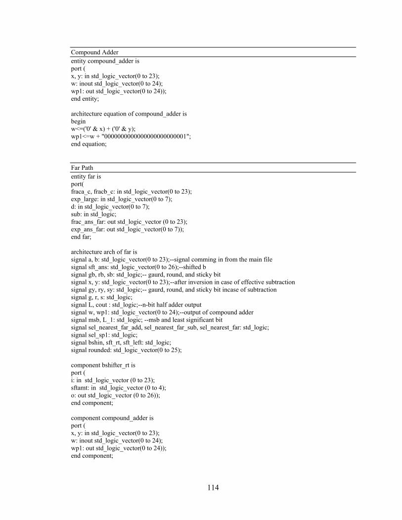
114
Compound Adder entity compound_adder is port ( x, y: in std_logic_vector(0 to 23); w: inout std_logic_vector(0 to 24); wp1: out std_logic_vector(0 to 24)); end entity; architecture equation of compound_adder is begin w<=('0' & x) + ('0' & y); wp1<=w + "0000000000000000000000001"; end equation; Far Path entity far is port( fraca_c, fracb_c: in std_logic_vector(0 to 23); exp_large: in std_logic_vector(0 to 7); d: in std_logic_vector(0 to 7); sub: in std_logic; frac_ans_far: out std_logic_vector (0 to 23); exp_ans_far: out std_logic_vector(0 to 7)); end far; architecture arch of far is signal a, b: std_logic_vector(0 to 23);--signal comming in from the main file signal sft_ans: std_logic_vector(0 to 26);--shifted b signal gb, rb, sb: std_logic;-- gaurd, round, and sticky bit signal x, y: std_logic_vector(0 to 23);--after inversion in case of effective subtraction signal gy, ry, sy: std_logic;-- gaurd, round, and sticky bit incase of subtraction signal g, r, s: std_logic; signal L, cout : std_logic;--n-bit half adder output signal w, wp1: std_logic_vector(0 to 24);--output of compound adder signal msb, L_1: std_logic; --msb and least significant bit signal sel_nearest_far_add, sel_nearest_far_sub, sel_nearest_far: std_logic; signal sel_sp1: std_logic; signal bshin, sft_rt, sft_left: std_logic; signal rounded: std_logic_vector(0 to 25); component bshifter_rt is port ( i: in std_logic_vector (0 to 23); sftamt: in std_logic_vector (0 to 4); o: out std_logic_vector (0 to 26)); end component; component compound_adder is port ( x, y: in std_logic_vector(0 to 23); w: inout std_logic_vector(0 to 24); wp1: out std_logic_vector(0 to 24)); end component;
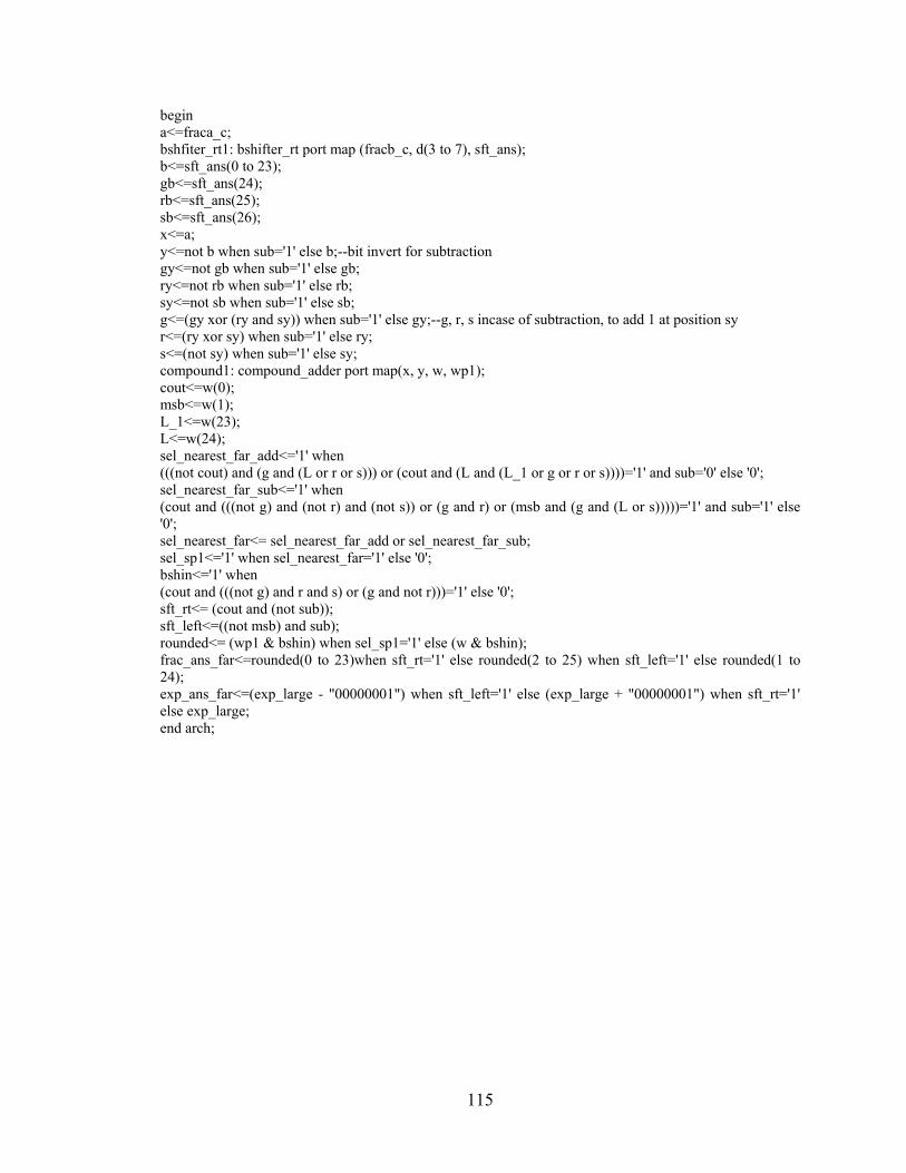
115
begin a<=fraca_c; bshfiter_rt1: bshifter_rt port map (fracb_c, d(3 to 7), sft_ans); b<=sft_ans(0 to 23); gb<=sft_ans(24); rb<=sft_ans(25); sb<=sft_ans(26); x<=a; y<=not b when sub='1' else b;--bit invert for subtraction gy<=not gb when sub='1' else gb; ry<=not rb when sub='1' else rb; sy<=not sb when sub='1' else sb; g<=(gy xor (ry and sy)) when sub='1' else gy;--g, r, s incase of subtraction, to add 1 at position sy r<=(ry xor sy) when sub='1' else ry; s<=(not sy) when sub='1' else sy; compound1: compound_adder port map(x, y, w, wp1); cout<=w(0); msb<=w(1); L_1<=w(23); L<=w(24); sel_nearest_far_add<='1' when (((not cout) and (g and (L or r or s))) or (cout and (L and (L_1 or g or r or s))))='1' and sub='0' else '0'; sel_nearest_far_sub<='1' when (cout and (((not g) and (not r) and (not s)) or (g and r) or (msb and (g and (L or s)))))='1' and sub='1' else '0'; sel_nearest_far<= sel_nearest_far_add or sel_nearest_far_sub; sel_sp1<='1' when sel_nearest_far='1' else '0'; bshin<='1' when (cout and (((not g) and r and s) or (g and not r)))='1' else '0'; sft_rt<= (cout and (not sub)); sft_left<=((not msb) and sub); rounded<= (wp1 & bshin) when sel_sp1='1' else (w & bshin); frac_ans_far<=rounded(0 to 23)when sft_rt='1' else rounded(2 to 25) when sft_left='1' else rounded(1 to 24); exp_ans_far<=(exp_large - "00000001") when sft_left='1' else (exp_large + "00000001") when sft_rt='1' else exp_large; end arch;