Embed Size (px)
Citation preview
Research ArticleFrequency-Tunable Electromagnetic Absorber by MechanicallyControlling Substrate Thickness
Heijun Jeong,1 Manos M. Tentzeris ,2 and Sungjoon Lim 1
1School of Electrical and Electronics Engineering, College of Engineering, Chung-Ang University, Seoul 156-756, Republic of Korea2School of Electrical and Computer Engineering, Georgia Institute of Technology, Atlanta, GA 30332-0250, USA
Correspondence should be addressed to Manos M. Tentzeris; [email protected] and Sungjoon Lim; [email protected]
Received 19 March 2018; Accepted 28 May 2018; Published 29 August 2018
Academic Editor: Atsushi Mase
Copyright © 2018 Heijun Jeong et al. This is an open access article distributed under the Creative Commons Attribution License,which permits unrestricted use, distribution, and reproduction in any medium, provided the original work is properly cited.
In this paper, we propose a frequency-tunable electromagnetic absorber that uses the mechanical control of substrate thickness. Theabsorption frequency of the proposed absorber can be changed by varying the substrate thickness. In order to mechanically controlthe substrate thickness, we introduce a 3D-printed molding with air space. The proposed structure consists of two layers and oneframe: the FR4 substrate, polylactic acid (PLA) frame, and air substrate. The FR4 and PLA thicknesses are fixed, and the airthickness is varied using the PLA frame. Therefore, the effective dielectric constant of the overall substrate can be changed. Themetallic rectangular patch and ground are patterned on the top and bottom FR4 substrates, respectively. The performance of theproposed tunable absorber is demonstrated from full-wave simulation and measurements. When both of the FR4 substratethicknesses are 0.3mm and the air thickness is changed from 1 to 3.5mm, the absorption frequency is changed from 8.9 to8.0 GHz, respectively. Therefore, the frequency-tuning capability of the proposed absorber is successfully demonstrated.
1. Introduction
Metamaterials are artificial structures in which periodic unitcells are infinitely arranged. Using these metamaterials, wecan control the characteristics of a material [1]. These tech-nologies are used in various fields, such as stealth technology[2, 3], electromagnetic interference (EMI) and electromag-netic compatibility (EMC) solutions [4], superlenses [5, 6],RF circuit applications [7], and sound wave technology[8]. Metamaterial absorbers are also one of its promisingapplications. The metamaterial absorber was first proposedby Landy et al. [9]. The previous absorbers, such as ferrite[10–13] or wedge-tapered [14, 15] absorbers, were bulky and,therefore, were limited by space. Compared to material-based electromagnetic (EM) absorbers, structure-basedmeta-material absorbers show high absorption rates, low pro-duction costs, and functionality with a low profile.
In spite of the several advantages of the metamaterialabsorber, it has the disadvantage of a narrow bandwidth,because it uses electromagnetic resonance. Therefore, in
order to overcome this disadvantage, metamaterial absorbershave been designed using lossy patterns [16–18], multire-sonance [19–21], and lumped components [22–24], inorder to broaden the absorption frequencies. A frequency-tunable metamaterial absorber is an alternative solution.The frequency-tunable metamaterial absorber can be usednot only as an electromagnetic absorber but also as afrequency-selective sensor. Most frequency-tunable metama-terial absorbers have been realized using electronic devicessuch as diodes [25–27], microelectromechanical systems(MEMS) [28–30], and liquid crystal technology [31, 32].Recently, fluidically tunable metamaterial absorbers havebeen proposed using liquid metal [33–35]. These electricallytunable devices show an instantaneous response. However,they are not only costly but also have limitations of designin a periodic structure because of additional DC bias linesand an extremely large number of devices. Alternatively,frequency-tunable metamaterial absorbers using liquid crys-tal or liquid metal can be fabricated not only on hard sub-strates but also on flexible substrates. In spite of its slow
HindawiInternational Journal of Antennas and PropagationVolume 2018, Article ID 1963051, 7 pageshttps://doi.org/10.1155/2018/1963051
tuning speed, this type of tunable absorbers has drawn inter-est due to its flexibility and simple design.
Recently, mechanically tunable metamaterial absorbershave been proposed using stretching technology [36–38].For instance, the physical size of the unit cell can bedeformed by stretching the substrate. Its tuning speed isslow, but it has a simple design and low cost for a periodicstructure. Because the absorption frequency can be deter-mined by the deformation level, a mechanically tunableabsorber can be used for frequency tunability as well asphysical strain sensors.
In this paper, we proposed a novel frequency-tunable EMabsorber by mechanically controlling the substrate thickness.The proposed thickness-controllable substrate consists of theFR4 layer with fixed thickness and the air layer with control-lable thickness. In order to mechanically control the thick-ness of the substrate, a polylactic acid (PLA) frame using a3D printer was fabricated. The frequency tunability of theproposed EM absorber is successfully demonstrated throughfull-wave simulation and measurement.
2. Electromagnetic Absorber Design
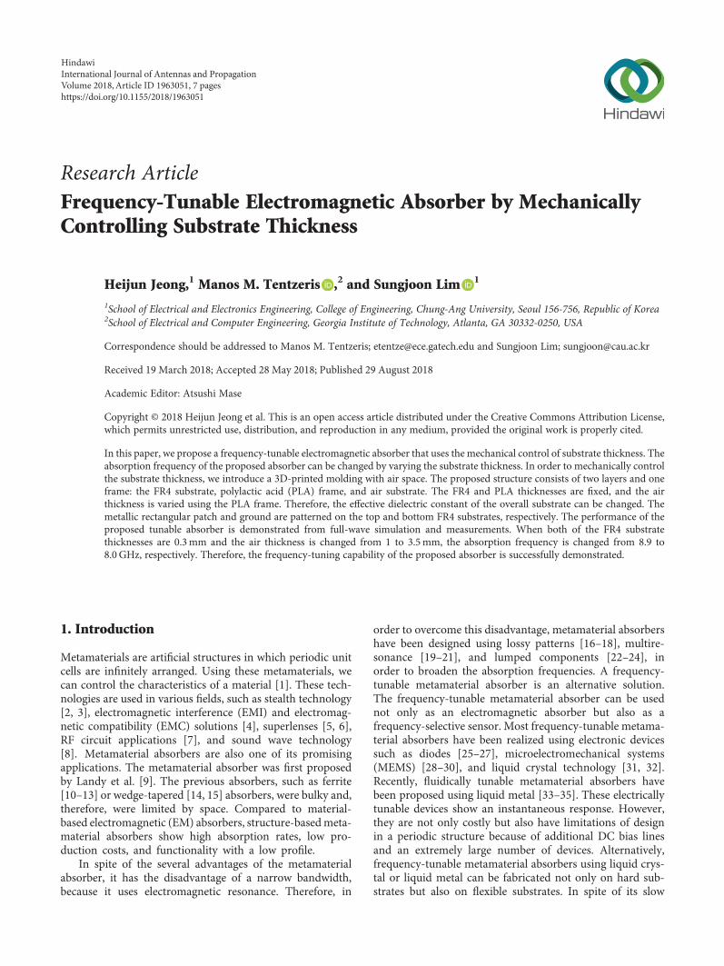
In this paper, we proposed a rectangular patch for the unitcell of the absorber. Figure 1 shows the geometry of a unit cellof the proposed absorber with geometrical dimensions. Theunit cell size (Ws×Ws) is 12mm× 12mm. The proposedabsorber is composed of two FR-4 substrates with the air sub-strate in between, as illustrated in Figure 1(b). The dielectric
constant and tangent loss of the FR-4 substrate are 4.4 and0.02, respectively. The patch is designed on the top of theupper FR-4 substrate. The ground plane is designed on thebottom FR-4 substrate. Both FR-4 substrates have a fixedthickness (H2 and H3) of 0.5mm. The air substrate thick-ness (H1) can be varied from 1.5mm to 3.5mm. In thiswork, the patch size is fixed, and the substrate thickness
Conductor FR-4 substrate
WsLp
Wp
Ws
(a)
Conductor FR-4 substrateAir
H (y) E (x)
k (z)
H1
(b)
FR-4 substrateAir
H2
H3
(c)
Figure 1: Geometry of the unit cell of the proposed absorber. (a) Top view of the unit cell. (b) Perspective view of the unit cell. (c) Side view ofthe unit cell. Ws = 12mm; Lp = 8mm; Wp = 7mm; H1 = 1 5mm; H2 =H3 = 0 5mm.
0
−2
−4
−6
Refle
ctio
n co
effici
ent (
dB)
−8
−10
−12
−14
−16
7 8 9Frequency (GHz)
10
Air thickeness = 1.5 mmAir thickeness = 2.5 mmAir thickeness = 3.5 mm
11
Figure 2: Simulated reflection coefficients of the proposed absorberat different air thicknesses.
2 International Journal of Antennas and Propagation
is varied. In particular, when the thickness of the air sub-strate is varied, Hs and εef f are changed, thereby changingthe resonant frequency.
3. Simulation Results
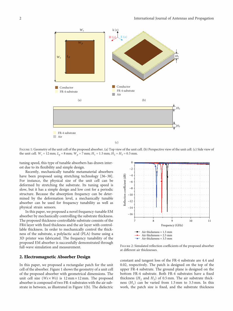
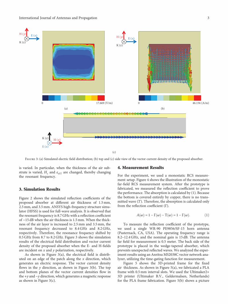
Figure 2 shows the simulated reflection coefficients of theproposed absorber at different air thickness of 1.5mm,2.5mm, and 3.5mm. ANSYS high-frequency structure simu-lator (HFSS) is used for full-wave analysis. It is observed thatthe resonant frequency is 8.7GHz with a reflection coefficientof −15 dB when the air thickness is 1.5mm. When the thick-ness of the air layer is increased to 2.5mm and 3.5mm, theresonant frequency decreased to 8.4GHz and 8.2GHz,respectively. Therefore, the resonance frequency shifted by0.5GHz from 8.7 to 8.2GHz. Figure 3 shows the simulationresults of the electrical field distribution and vector currentdensity of the proposed absorber when the E- and H-fieldsare incident on x and y polarization, respectively.
As shown in Figure 3(a), the electrical field is distrib-uted on an edge of the patch along the x direction, whichgenerates an electric response. The vector current densityflows in the y direction, as shown in Figure 3(b). The topand bottom planes of the vector current densities flow inthe +y and −y direction, which generates a magnetic responseas shown in Figure 3(c).
4. Measurement Results
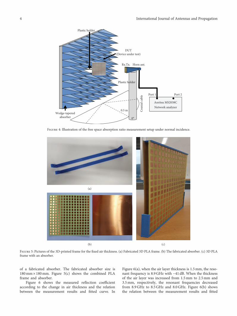
For the experiment, we used a monostatic RCS measure-ment setup. Figure 4 shows the illustration of the monostaticfar-field RCS measurement system. After the prototype isfabricated, we measured the reflection coefficient to provethe performance. The absorption is calculated by (1). Becausethe bottom is covered entirely by copper, there is no trans-mitted wave (Τ). Therefore, the absorption is calculated onlyfrom the reflection coefficient (Γ).
A ω = 1 − Γ ω − Τ ω = 1 − Γ ω 1
To measure the reflection coefficient of the prototype,we used a single WR-90 PE9856/SF-15 horn antenna(Pasternack, CA, USA). The operating frequency range is8.2–12.4GHz, and the nominal gain is 15 dB. The antennafar field for measurement is 0.5 meter. The back side of theprototype is placed in the wedge-tapered absorber, whichprevents unexpected reflected waves. We analyzed the exper-iment results using an Anritsu MS2038C vector network ana-lyzer, utilizing the time-gating function for measurement.
Figure 5 shows the 3D-printed frame for the fixedair thickness. As shown in Figure 5(a), we fabricated a PLAframe with 0.5mm interval slots. We used the Ultimaker2+3D printer (Ultimaker B.V., Geldermalsen, Netherlands)for the PLA frame fabrication. Figure 5(b) shows a picture
0 17.669 (V/m)
E (x)H (y)
K (z)
(a)
E (x)H (y)
K (z)
0 46.156 (A/m)
(b)
H (y)K (z)
E (x)
(c)
Figure 3: (a) Simulated electric field distribution; (b) top and (c) side view of the vector current density of the proposed absorber.
3International Journal of Antennas and Propagation
of a fabricated absorber. The fabricated absorber size is180mm× 180mm. Figure 5(c) shows the combined PLAframe and absorber.
Figure 6 shows the measured reflection coefficientaccording to the change in air thickness and the relationbetween the measurement results and fitted curve. In
Figure 6(a), when the air layer thickness is 1.5mm, the reso-nant frequency is 8.9GHz with −41 dB. When the thicknessof the air layer was increased from 1.5mm to 2.5mm and3.5mm, respectively, the resonant frequencies decreasedfrom 8.9GHz to 8.5GHz and 8.0GHz. Figure 6(b) showsthe relation between the measurement results and fitted
(a)
(b) (c)
Figure 5: Pictures of the 3D-printed frame for the fixed air thickness. (a) Fabricated 3D PLA frame. (b) The fabricated absorber. (c) 3D PLAframe with an absorber.
Anritsu MS2038CNetwork analyzer
Port 2
Coax
ial c
able
Wedge-taperedabsorber
Port 1
0.5 m
0°
Plastic holder
Plastic holder
DUT(Device under test)
Horn ant.Rx.Tx.
Figure 4: Illustration of the free space absorption ratio measurement setup under normal incidence.
4 International Journal of Antennas and Propagation
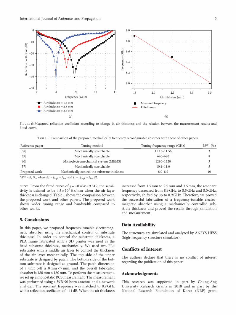
curve. From the fitted curve of y=−0.45x+9.519, the sensi-tivity is defined to be 4.5× 10⁸Hz/mm when the air layerthickness is changed. Table 1 shows the comparison betweenthe proposed work and other papers. The proposed workshows wider tuning range and bandwidth compared toother works.
5. Conclusions
In this paper, we proposed frequency-tunable electromag-netic absorber using the mechanical control of substratethickness. In order to control the substrate thickness, aPLA frame fabricated with a 3D printer was used as thefixed substrate thickness, mechanically. We used two FR4substrates with a middle air layer to control the thicknessof the air layer mechanically. The top side of the uppersubstrate is designed by patch. The bottom side of the bot-tom substrate is designed as ground. The patch dimensionof a unit cell is 8mm× 7mm, and the overall fabricatedabsorber is 180mm× 180mm. To perform the measurement,we set up a monostatic RCS measurement. The measurementwas performed using a WR-90 horn antenna and a networkanalyzer. The resonant frequency was matched to 8.9GHzwith a reflection coefficient of −41dB. When the air thickness
increased from 1.5mm to 2.5mm and 3.5mm, the resonantfrequency decreased from 8.9GHz to 8.5GHz and 8.0GHz,respectively, shifted by up to 0.9GHz. Therefore, we provedthe successful fabrication of a frequency-tunable electro-magnetic absorber using a mechanically controlled sub-strate thickness and proved the results through simulationand measurement.
Data Availability
The structures are simulated and analyzed by ANSYS HFSS(high-frequency structure simulator).
Conflicts of Interest
The authors declare that there is no conflict of interestregarding the publication of this paper.
Acknowledgments
This research was supported in part by Chung-AngUniversity Research Grants in 2018 and in part by theNational Research Foundation of Korea (NRF) grant
Table 1: Comparison of the proposed mechanically frequency reconfigurable absorber with those of other papers.
Reference paper Tuning method Tuning frequency range (GHz) BW∗ (%)
[38] Mechanically stretchable 11.15–11.56 3
[39] Mechanically stretchable 640–680 8
[40] Microelectromechanical system (MEMS) 1280–1320 3
[37] Mechanically stretchable 10.4–11.0 5
Proposed work Mechanically control the substrate thickness 8.0–8.9 10∗BW = Δf /f c, where Δf = f high − f low and f c = f high + f low /2.
Refle
ctio
n co
effici
ent (
dB)
−507 8 9
Frequency (GHz)
Air thickness = 1.5 mmAir thickness = 2.5 mmAir thickness = 3.5 mm
10 11
−40
−30
−20
−10
0
(a)
Freq
uenc
y (G
Hz)
Measured frequencyFitted curve
9.0
8.8
8.6
8.4
8.2
8.0
1.5 2.0Air thickness (mm)
2.5 3.0 3.5
(b)
Figure 6: Measured reflection coefficient according to change in air thickness and the relation between the measurement results andfitted curve.
5International Journal of Antennas and Propagation
funded by the Korean government (MSIP) (no.2017R1A2B3003856).
References
[1] C. M. Watts, X. L. Liu, and W. J. Padilla, “Metamaterial elec-tromagnetic wave absorbers,” Advanced Materials, vol. 24,no. 23, pp. OP98–OP120, 2012.
[2] D. Schurig, J. J. Mock, B. J. Justice et al., “Metamaterial electro-magnetic cloak at microwave frequencies,” Science, vol. 314,no. 5801, pp. 977–980, 2006.
[3] K. Iwaszczuk, A. C. Strikwerda, K. Fan, X. Zhang, R. D. Averitt,and P. U. Jepsen, “Flexible metamaterial absorbers for stealthapplications at terahertz frequencies,” Optics Express, vol. 20,no. 1, pp. 635–643, 2012.
[4] S. Shahparnia and O. M. M. Ramahi, “Electromagnetic inter-ference (EMI) reduction from printed circuit boards (PCB)using electromagnetic bandgap structures,” IEEE Transactionson Electromagnetic Compatibility, vol. 46, no. 4, pp. 580–587,2004.
[5] N. Fang, H. Lee, C. Sun, and X. Zhang, “Sub–diffraction-lim-ited optical imaging with a silver superlens,” Science, vol. 308,no. 5721, pp. 534–537, 2005.
[6] K. Aydin, I. Bulu, and E. Ozbay, “Subwavelength resolutionwith a negative-index metamaterial superlens,” Applied Phys-ics Letters, vol. 90, no. 25, article 254102, 2007.
[7] D.-S. Eom and H.-Y. Lee, “A broadband half-mode substrateintegrated waveguide quadrature Wilkinson power dividerusing composite right/left-handed transmission line,” Journalof Electromagnetic Engineering and Science, vol. 17, no. 1,pp. 9–13, 2017.
[8] Z. Yang, H. M. Dai, N. H. Chan, G. C. Ma, and P. Sheng,“Acoustic metamaterial panels for sound attenuation in the50–1000 Hz regime,” Applied Physics Letters, vol. 96, no. 4,article 041906, 2010.
[9] N. I. Landy, S. Sajuyigbe, J. J. Mock, D. R. Smith, and W. J.Padilla, “Perfect metamaterial absorber,” Physical ReviewLetters, vol. 100, no. 20, article 207402, 2008.
[10] M.-J. Park, J. Choi, and S.-S. Kim, “Wide bandwidth pyramidalabsorbers of granular ferrite and carbonyl iron powders,” IEEETransactions on Magnetics, vol. 36, no. 5, pp. 3272–3274, 2000.
[11] J. Y. Shin and J. H. Oh, “The microwave absorbing phenomenaof ferrite microwave absorbers,” IEEE Transactions on Mag-netics, vol. 29, no. 6, pp. 3437–3439, 1993.
[12] K. Hatakeyama and T. Inui, “Electromagnetic wave absorberusing ferrite absorbing material dispersed with short metalfibers,” IEEE Transactions on Magnetics, vol. 20, no. 5,pp. 1261–1263, 1984.
[13] D.-Y. Kim, Y.-H. Yoon, K.-J. Jo, G.-B. Jung, and C.-C. An,“Effects of sheet thickness on the electromagnetic waveabsorbing characterization of Li0.375Ni0.375Zn0.25-ferrite com-posite as a radiation absorbent material,” Journal of Electro-magnetic Engineering and Science, vol. 16, no. 3, pp. 150–158,2016.
[14] J. W. Head, “The design of gradual transition (wedge)absorbers for a free-field room,” British Journal of AppliedPhysics, vol. 16, no. 7, pp. 1009–1014, 1965.
[15] C. L. Holloway and E. F. Kuester, “A low-frequency model forwedge or pyramid absorber arrays-II: computed and measuredresults,” IEEE Transactions on Electromagnetic Compatibility,vol. 36, no. 4, pp. 307–313, 1994.
[16] H.-B. Zhang, P.-H. Zhou, H.-P. Lu, Y.-Q. Xu, D.-F. Liang,and L.-J. Deng, “Resistance selection of high impedance sur-face absorbers for perfect and broadband absorption,” IEEETransactions on Antennas and Propagation, vol. 61, no. 2,pp. 976–979, 2013.
[17] F. A. Costa and A. Monorchio, “A frequency selective radomewith wideband absorbing properties,” IEEE Transactions onAntennas and Propagation, vol. 60, no. 6, pp. 2740–2747, 2012.
[18] J. Lee and B. Lee, “Design of thin RC absorbers using a silvernanowire resistive screen,” Journal of Electromagnetic Engi-neering and Science, vol. 16, no. 2, pp. 106–111, 2016.
[19] H. Luo, X. Hu, Y. Qiu, and P. Zhou, “Design of a wide-bandnearly perfect absorber based on multi-resonance with squarepatch,” Solid State Communications, vol. 188, pp. 5–11, 2014.
[20] J. W. Park, P. van Tuong, J. Y. Rhee et al., “Multi-band meta-material absorber based on the arrangement of donut-type res-onators,” Optics Express, vol. 21, no. 8, pp. 9691–9702, 2013.
[21] X. Y. Peng, B. Wang, S. Lai, D. H. Zhang, and J. H. Teng,“Ultrathin multi-band planar metamaterial absorber basedon standing wave resonances,” Optics Express, vol. 20, no. 25,pp. 27756–27765, 2012.
[22] C. Mias and J. H. Yap, “A varactor-tunable high impedancesurface with a resistive-lumped-element biasing grid,” IEEETransactions on Antennas and Propagation, vol. 55, no. 7,pp. 1955–1962, 2007.
[23] F. Costa, A. Monorchio, and G. Manara, “Analysis and designof ultra thin electromagnetic absorbers comprising resistivelyloaded high impedance surfaces,” IEEE Transactions onAntennas and Propagation, vol. 58, no. 5, pp. 1551–1558, 2010.
[24] Y. Z. Cheng, Y. Wang, Y. Nie, R. Z. Gong, X. Xiong, andX. Wang, “Design, fabrication and measurement of a broad-band polarization-insensitive metamaterial absorber basedon lumped elements,” Journal of Applied Physics, vol. 111,no. 4, article 044902, 2012.
[25] A. Tennant and B. Chambers, “Adaptive radar absorbingstructure with PIN diode controlled active frequency selectivesurface,” Smart Materials and Structures, vol. 13, no. 1,pp. 122–125, 2004.
[26] W. Xu and S. Sonkusale, “Microwave diode switchable meta-material reflector/absorber,” Applied Physics Letters, vol. 103,no. 3, article 031902, 2013.
[27] A. Tennant and B. Chambers, “A single-layer tuneable micro-wave absorber using an active FSS,” IEEE Microwave andWireless Components Letters, vol. 14, no. 1, pp. 46-47, 2004.
[28] H. Tao, A. C. Strikwerda, K. Fan, W. J. Padilla, X. Zhang, andR. D. Averitt, “MEMS based structurally tunable metamateri-als at terahertz frequencies,” Journal of Infrared, Millimeter,and Terahertz Waves, vol. 32, no. 5, pp. 580–595, 2011.
[29] H. Bilgin, S. Zahertar, S. Sadeghzadeh, A. D. Yalcinkaya,and H. Torun, “A MEMS-based terahertz detector withmetamaterial-based absorber and optical interferometric read-out,” Sensors and Actuators A: Physical, vol. 244, no. 15,pp. 292–298, 2016.
[30] T. Y. Li, L. Wang, J. M. Wang, S. Li, and X. J. He, “A dual bandpolarization-insensitive tunable absorber based on terahertzMEMS metamaterial,” Integrated Ferroelectrics, vol. 151,no. 1, pp. 157–163, 2014.
[31] G. Isić, B. Vasić, D. C. Zografopoulos, R. Beccherelli, andR. Gajić, “Electrically tunable critically coupled terahertz meta-material absorber based on nematic liquid crystals,” PhysicalReview Applied, vol. 3, no. 6, article 064007, 2015.
6 International Journal of Antennas and Propagation
[32] D. Shrekenhamer, W. C. Chen, and W. J. Padilla, “Liquidcrystal tunable metamaterial absorber,” Physical Review Let-ters, vol. 110, no. 17, article 177403, 2013.
[33] K. Ling, H. Kim, M. Yoo, and S. Lim, “Frequency-switch-able metamaterial absorber injecting eutectic gallium-indium(EGaIn) liquid metal alloy,” Sensors, vol. 15, no. 11,pp. 28154–28165, 2015.
[34] K. Kim, D. Lee, S. Eom, and S. Lim, “Stretchable metamaterialabsorber using liquid metal-filled polydimethylsiloxane(PDMS),” Sensors, vol. 16, no. 4, p. 521, 2016.
[35] H. K. Kim, D. Lee, and S. Lim, “Wideband-switchablemetamaterial absorber using injected liquid metal,” ScientificReports, vol. 6, no. 1, article 31823, 2016.
[36] S. Yang, P. Liu, M. Yang, Q. Wang, J. Song, and L. Dong,“From flexible and stretchable meta-atom to metamaterial : awearable microwave meta-skin with tunable frequency selec-tive and cloaking effects,” Scientific Reports, vol. 6, no. 1,pp. 21921–21929, 2016.
[37] H. Jeong and S. Lim, “A stretchable electromagnetic absorberfabricated using screen printing technology,” Sensors, vol. 17,no. 5, pp. 1175–1184, 2017.
[38] F. Zhang, S. Feng, K. Qiu et al., “Mechanically stretchable andtunable metamaterial absorber,” Applied Physics Letters,vol. 106, no. 9, article 091907, 2015.
[39] J. Li, C. M. Shah,W.Withayachumnankul et al., “Mechanicallytunable terahertz metamaterials,” Applied Physics Letters,vol. 102, no. 12, article 121101, 2013.
[40] F. Hu, Y. Qian, Z. Li et al., “Design of a tunable terahertz nar-rowband metamaterial absorber based on an electrostaticallyactuated MEMS cantilever and split ring resonator array,”Journal of Optics, vol. 15, no. 5, article 055101, 2013.
7International Journal of Antennas and Propagation

International Journal of
AerospaceEngineeringHindawiwww.hindawi.com Volume 2018
RoboticsJournal of
Hindawiwww.hindawi.com Volume 2018
Hindawiwww.hindawi.com Volume 2018
Active and Passive Electronic Components
VLSI Design
Hindawiwww.hindawi.com Volume 2018
Hindawiwww.hindawi.com Volume 2018
Shock and Vibration
Hindawiwww.hindawi.com Volume 2018
Civil EngineeringAdvances in
Acoustics and VibrationAdvances in
Hindawiwww.hindawi.com Volume 2018
Hindawiwww.hindawi.com Volume 2018
Electrical and Computer Engineering
Journal of
Advances inOptoElectronics
Hindawiwww.hindawi.com
Volume 2018
Hindawi Publishing Corporation http://www.hindawi.com Volume 2013Hindawiwww.hindawi.com
The Scientific World Journal
Volume 2018
Control Scienceand Engineering
Journal of
Hindawiwww.hindawi.com Volume 2018
Hindawiwww.hindawi.com
Journal ofEngineeringVolume 2018
SensorsJournal of
Hindawiwww.hindawi.com Volume 2018
International Journal of
RotatingMachinery
Hindawiwww.hindawi.com Volume 2018
Modelling &Simulationin EngineeringHindawiwww.hindawi.com Volume 2018
Hindawiwww.hindawi.com Volume 2018
Chemical EngineeringInternational Journal of Antennas and
Propagation
International Journal of
Hindawiwww.hindawi.com Volume 2018
Hindawiwww.hindawi.com Volume 2018
Navigation and Observation
International Journal of
Hindawi
www.hindawi.com Volume 2018
Advances in
Multimedia
Submit your manuscripts atwww.hindawi.com


![Journal of Sound and Vibration...The design principle of the nonlinear vibration absorber (NL-VA) From the results obtained by the previous studies [7e9,23e26], a tunable VA with adjustable](https://img.pdfslide.net/doc/110x75/60b8c81c212f1a6e00391244/journal-of-sound-and-vibration-the-design-principle-of-the-nonlinear-vibration.jpg)