Embed Size (px)
Citation preview
www.DataSheet4U.com
©2004 Fairchild Semiconductor Corporation
www.fairchildsemi.com
Rev.1.0.4
Features• Internal Avalanche Rugged Sense FET• Consumes only 0.65W at 240VAC & 0.3W load with
Advanced Burst-Mode Operation• Frequency Modulation for low EMI• Precision Fixed Operating Frequency• Internal Start-up Circuit• Pulse by Pulse Current Limiting• Abnormal Over Current Protection• Over Voltage Protection • Over Load Protection• Internal Thermal Shutdown Function• Auto-Restart Mode• Under Voltage Lockout• Low Operating Current (3mA)• Adjustable Peak Current Limit• Built-in Soft Start
Applications• SMPS for VCR, SVR, STB, DVD & DVCD• SMPS for Printer, Facsimile & Scanner• Adaptor for Camcorder
DescriptionThe FSDL0165RN is an integrated Pulse Width Modulator(PWM) and Sense FET specifically designed for high perfor-mance offline Switch Mode Power Supplies (SMPS) withminimal external components. This device is an integratedhigh voltage power switching regulator which combine anavalanche rugged Sense FET with a current mode PWMcontrol block. The integrated PWM controller featuresinclude: a fixed oscillator with frequency modulation forreduced EMI, Under Voltage Lock Out (UVLO) protection,Leading Edge Blanking (LEB), optimized gate turn-on/turn-off driver, Thermal Shut Down (TSD) protection, AbnormalOver Current Protection (AOCP) and temperature compen-sated precision current sources for loop compensation andfault protection circuitry. When compared to a discreteMOSFET and controller or RCC switching converter solu-tion, the FSDL0165RN reduce total component count,design size, weight and at the same time increases efficiency,productivity, and system reliability. This device is a basicplatform well suited for cost effective designs of flybackconverters.
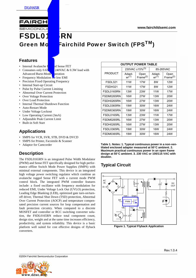
Table 1. Notes: 1. Typical continuous power in a non-ven-tilated enclosed adapter measured at 50°C ambient. 2. Maximum practical continuous power in an open frame design at 50°C ambient. 3. 230 VAC or 100/115 VAC with doubler.
Typical Circuit
Figure 1. Typical Flyback Application
OUTPUT POWER TABLE
PRODUCT230VAC ±15%(3) 85-265VACAdapt-er(1)
Open Frame(2)
Adapt-er(1)
Open Frame(2)
FSDL321 11W 17W 8W 12W
FSDH321 11W 17W 8W 12W
FSDL0165RN 13W 23W 11W 17W
FSDM0265RN 16W 27W 13W 20WFSDH0265RN 16W 27W 13W 20W
FSDL0365RN 19W 30W 16W 24W
FSDM0365RN 19W 30W 16W 24W
FSDL0165RL 13W 23W 11W 17WFSDM0265RL 16W 27W 13W 20W
FSDH0265RL 16W 27W 13W 20W
FSDL0365RL 19W 30W 16W 24W
FSDM0365RL 19W 30W 16W 24W
Drain
Source
Vstr
Vfb Vcc
PWM
ACIN DC
OUT
Ipk
FSDL0165RNGreen Mode Fairchild Power Switch (FPSTM)
查询DL0165R供应商查询DL0165R供应商
FSDL0165RN
2
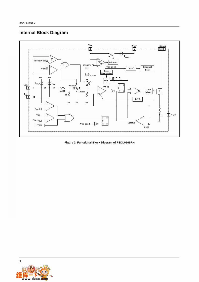
Internal Block Diagram
Figure 2. Functional Block Diagram of FSDL0165RN
8V/12V
2 6,7,8
1
3
Vref InternalBias
S
Q
Q
R
OSCVcc Vcc
Idelay IFB
VSD
TSD
Vovp
Vcc
Vocp
S
Q
Q
R
R2.5R
Vcc good
Vcc Drain
VFB
GND
AOCP
Gatedriver
5Vstr
Istart
Vcc good
VBURL/VBURH
LEB
PWM
Soft start
+
-
4Ipk
Freq.Modulation
VBURH Vcc
IB_PEAK
Burst
Normal
FSDL0165RN
3
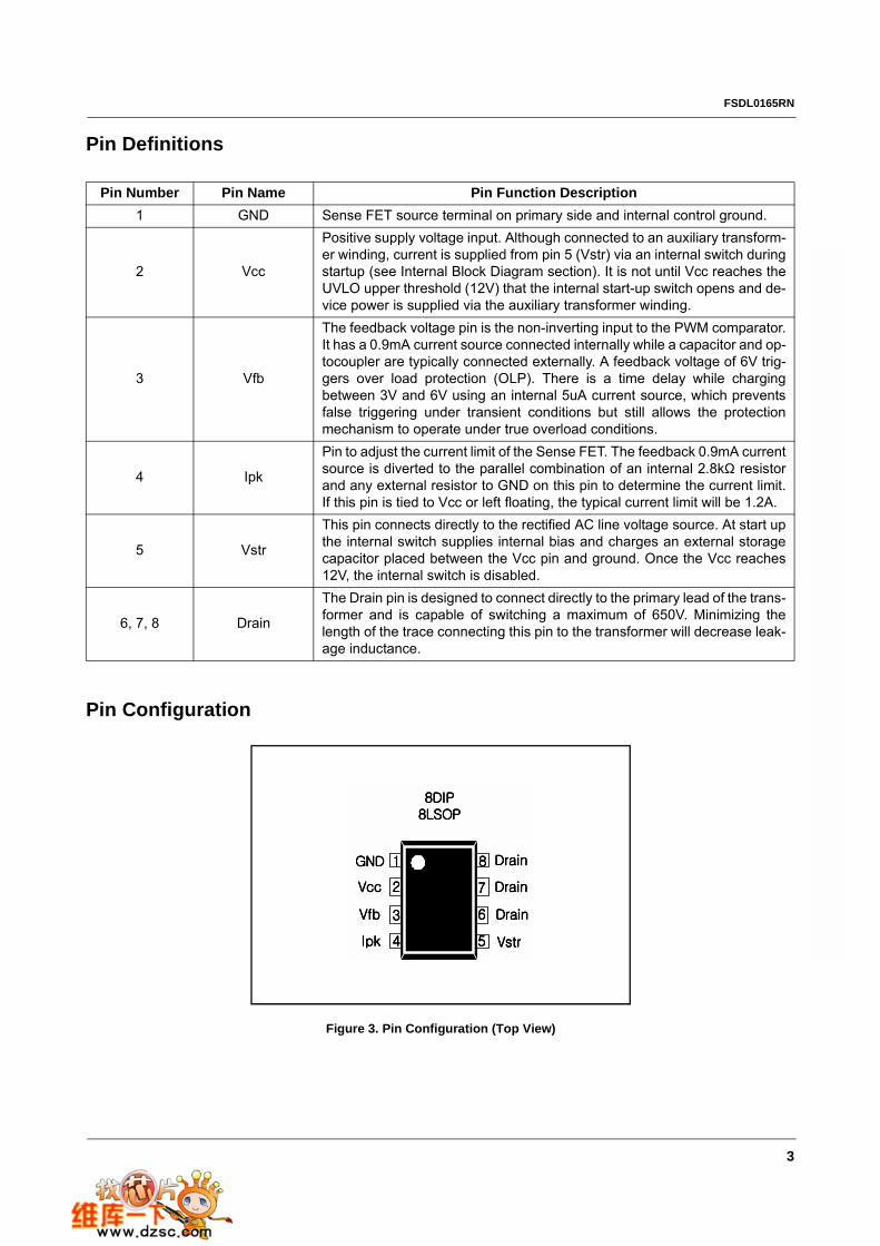
Pin Definitions
Pin Configuration
Figure 3. Pin Configuration (Top View)
Pin Number Pin Name Pin Function Description1 GND Sense FET source terminal on primary side and internal control ground.
2 Vcc
Positive supply voltage input. Although connected to an auxiliary transform-er winding, current is supplied from pin 5 (Vstr) via an internal switch duringstartup (see Internal Block Diagram section). It is not until Vcc reaches theUVLO upper threshold (12V) that the internal start-up switch opens and de-vice power is supplied via the auxiliary transformer winding.
3 Vfb
The feedback voltage pin is the non-inverting input to the PWM comparator.It has a 0.9mA current source connected internally while a capacitor and op-tocoupler are typically connected externally. A feedback voltage of 6V trig-gers over load protection (OLP). There is a time delay while chargingbetween 3V and 6V using an internal 5uA current source, which preventsfalse triggering under transient conditions but still allows the protectionmechanism to operate under true overload conditions.
4 Ipk
Pin to adjust the current limit of the Sense FET. The feedback 0.9mA currentsource is diverted to the parallel combination of an internal 2.8kΩ resistorand any external resistor to GND on this pin to determine the current limit.If this pin is tied to Vcc or left floating, the typical current limit will be 1.2A.
5 Vstr
This pin connects directly to the rectified AC line voltage source. At start upthe internal switch supplies internal bias and charges an external storagecapacitor placed between the Vcc pin and ground. Once the Vcc reaches12V, the internal switch is disabled.
6, 7, 8 Drain
The Drain pin is designed to connect directly to the primary lead of the trans-former and is capable of switching a maximum of 650V. Minimizing thelength of the trace connecting this pin to the transformer will decrease leak-age inductance.
1111
2222
3333
4444 5555
6666
7777
8888GNDGNDGNDGND
VccVccVccVcc
VfbVfbVfbVfb
IpkIpkIpkIpk VstrVstrVstrVstr
DrainDrainDrainDrain
DrainDrainDrainDrain
DrainDrainDrainDrain
8DIP8DIP8DIP8DIP8LSOP8LSOP8LSOP8LSOP
FSDL0165RN
4
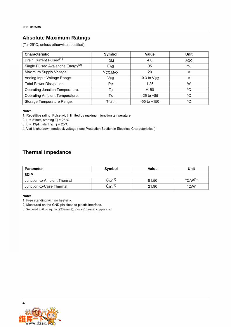
Absolute Maximum Ratings(Ta=25°C, unless otherwise specified)
Note:1. Repetitive rating: Pulse width limited by maximum junction temperature2. L = 51mH, starting Tj = 25°C3. L = 13µH, starting Tj = 25°C4. Vsd is shutdown feedback voltage ( see Protection Section in Electrical Characteristics )
Thermal Impedance
Note:1. Free standing with no heatsink.2. Measured on the GND pin close to plastic interface.3. Soldered to 0.36 sq. inch(232mm2), 2 oz.(610g/m2) copper clad.
Characteristic Symbol Value UnitDrain Current Pulsed(1) IDM 4.0 ADCSingle Pulsed Avalanche Energy(2) EAS 95 mJMaximum Supply Voltage VCC,MAX 20 VAnalog Input Voltage Range VFB -0.3 to VSD VTotal Power Dissipation PD 1.25 WOperating Junction Temperature. TJ +150 °COperating Ambient Temperature. TA -25 to +85 °CStorage Temperature Range. TSTG -55 to +150 °C
Parameter Symbol Value Unit8DIPJunction-to-Ambient Thermal θJA(1) 81.50 °C/W(3)
Junction-to-Case Thermal θJC(2) 21.90 °C/W

FSDL0165RN
5
Electrical Characteristics (Ta = 25°C unless otherwise specified)
Parameter Symbol Condition Min. Typ. Max. Unit
Sense FET SECTION
Startup Voltage (Vstr) Breakdown BVSTR VCC=0V, ID=1mA 650 - - V
Drain-Source Breakdown Voltage BVDSS VGS=0V, ID=50µA 650 - - V
Off-State Current(Max.Rating =660V) IDSS
VDS=660V, VGS=0V - - 50 µA
VDS=0.8Max.Rating VGS=0V, TC=125°C - - 200 µA
On-State Resistance(1) RDS(ON) VGS=10V, ID=0.5A - 8.0 10.0 Ω
Input Capacitance CISSVGS=0V, VDS=25V,F=1MHz
- 250 - pF
Output Capacitance COSS - 25 - pF
Reverse Transfer Capacitance CRSS - 10 - pF
Turn On Delay Time TD(ON) VDS=325V, ID=1.0A (Sense FET switching time is essentially independent of operating temperature)
- 12 - ns
Rise Time TR - 4 - ns
Turn Off Delay Time TD(OFF) - 30 - ns
Fall Time TF - 10 - ns
CONTROL SECTION
Output Frequency FOSC FSDL0165R
45 50 55 KHz
Output Frequency Modulation FMOD ±1.0 ±.1.5 ±2.0 KHz
Frequency Change With Temperature(2) - -25°C ≤ Ta ≤ 85°C - ±5 ±10 %
Maximum Duty Cycle DMAX FSDL0165R 71 77 83 %
Minimum Duty Cycle DMIN 0 0 0 %
Start threshold voltage VSTART VFB=GND 11 12 13 V
Stop threshold voltage VSTOP VFB=GND 7 8 9 V
Feedback Source Current IFB VFB=GND 0.7 0.9 1.1 mA
Internal Soft Start Time TS/S VFB=4V 10 15 20 ms
BURST MODE SECTION
Burst Mode Voltages VBURH - 0.5 0.6 0.7 V
VBURL - 0.25 0.35 0.45 V
PROTECTION SECTION
Drain to Source Peak Current Limit IOVER Max. inductor current 1.06 1.20 1.35 A
Current Limit Delay(3) TCLD - 500 - ns
Thermal Shutdown TSD - 125 140 - °C
FSDL0165RN
6
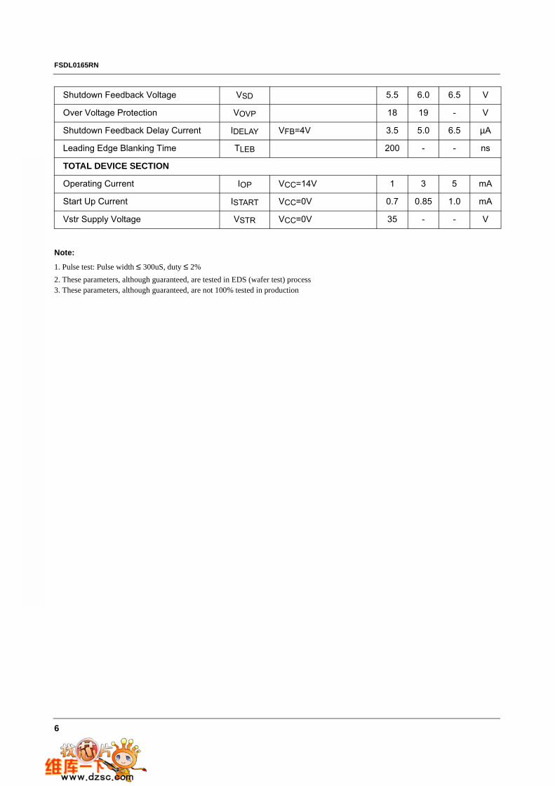
Note:
1. Pulse test: Pulse width ≤ 300uS, duty ≤ 2% 2. These parameters, although guaranteed, are tested in EDS (wafer test) process3. These parameters, although guaranteed, are not 100% tested in production
Shutdown Feedback Voltage VSD 5.5 6.0 6.5 V
Over Voltage Protection VOVP 18 19 - V
Shutdown Feedback Delay Current IDELAY VFB=4V 3.5 5.0 6.5 µA
Leading Edge Blanking Time TLEB 200 - - ns
TOTAL DEVICE SECTION
Operating Current IOP VCC=14V 1 3 5 mA
Start Up Current ISTART VCC=0V 0.7 0.85 1.0 mA
Vstr Supply Voltage VSTR VCC=0V 35 - - V

FSDL0165RN
7
Comparison Between KA5x0165RN and FSDL0165RNFunction KA5x0265RN FSDL0165RN FSDL0165RN AdvantagesSoft-Start not applicable 15mS Gradually increasing current limit
during soft-start further reduces peak current and voltage component stresses
Eliminates external components used for soft-start in most applications
Reduces or eliminates output overshoot
External Current Limit not applicable Programmable of default current limit
Smaller transformer Allows power limiting (constant over-
load power) Allows use of larger device for lower
losses and higher efficiency.Frequency Modulation not applicable ±1.5KHz @50KHz Reduced conducted EMIBurst Mode Operation not applicable Yes-built into
controller Improve light load efficiency Reduces no-load consumption Transformer audible noise reduction
Drain Creepage at Package
1,02mm 7.62mm Greater immunity to arcing as a result of build-up of dust, debris and other contaminants
FSDL0165RN
8
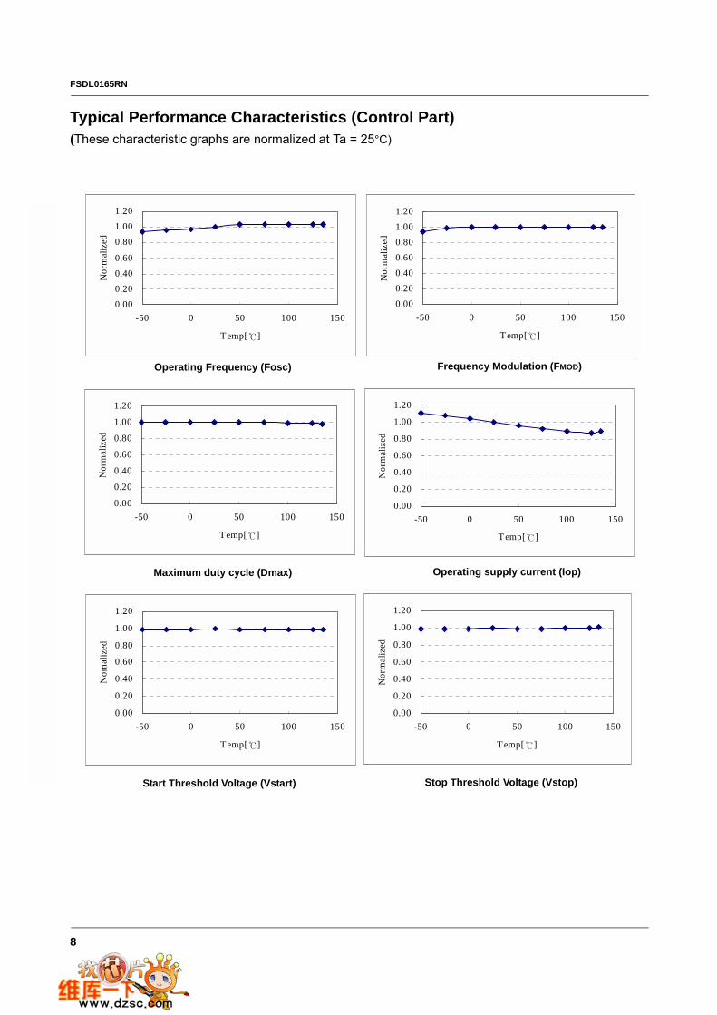
Typical Performance Characteristics (Control Part)(These characteristic graphs are normalized at Ta = 25°C)
0.00
0.200.40
0.60
0.801.00
1.20
-50 0 50 100 150
Temp[]
Nor
mal
ized
Operating Frequency (Fosc)
0.00
0.200.40
0.600.801.00
1.20
-50 0 50 100 150
T emp[]
Nor
mal
ized
Frequency Modulation (FMOD)
0.00
0.20
0.40
0.60
0.80
1.00
1.20
-50 0 50 100 150
Temp[]
Nor
mal
ized
Maximum duty cycle (Dmax)
0.00
0.20
0.40
0.60
0.80
1.00
1.20
-50 0 50 100 150
T emp[]
Nor
mal
ized
Operating supply current (Iop)
0.00
0.20
0.40
0.60
0.80
1.00
1.20
-50 0 50 100 150
Temp[]
Nom
aliz
ed
Start Threshold Voltage (Vstart)
0.00
0.20
0.40
0.60
0.80
1.00
1.20
-50 0 50 100 150
T emp[]
Nor
mal
ized
Stop Threshold Voltage (Vstop)
FSDL0165RN
9
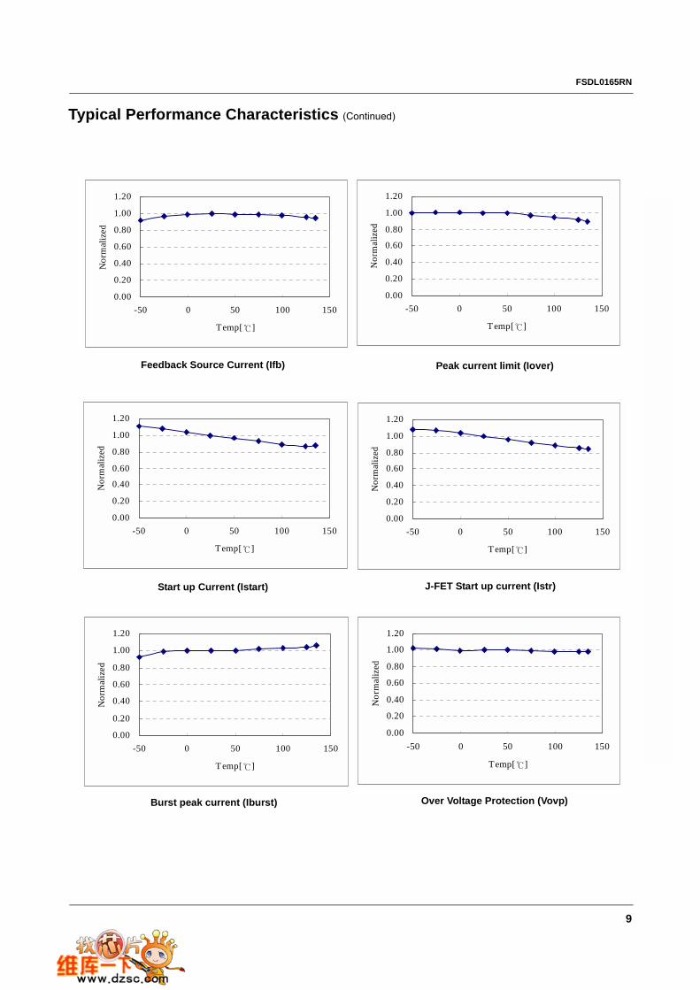
Typical Performance Characteristics (Continued)
0.00
0.20
0.40
0.60
0.80
1.00
1.20
-50 0 50 100 150
Temp[]
Nor
mal
ized
Feedback Source Current (Ifb)
0.00
0.20
0.40
0.60
0.80
1.00
1.20
-50 0 50 100 150
T emp[]
Nor
mal
ized
Peak current limit (Iover)
0.00
0.20
0.40
0.60
0.80
1.00
1.20
-50 0 50 100 150
Temp[]
Nor
mal
ized
Start up Current (Istart)
0.00
0.20
0.40
0.60
0.80
1.00
1.20
-50 0 50 100 150
T emp[]
Nor
mal
ized
J-FET Start up current (Istr)
0.00
0.20
0.40
0.60
0.80
1.00
1.20
-50 0 50 100 150
T emp[]
Nor
mal
ized
Burst peak current (Iburst)
0.00
0.20
0.40
0.60
0.80
1.00
1.20
-50 0 50 100 150
Temp[]
Nor
mal
ized
Over Voltage Protection (Vovp)
FSDL0165RN
10
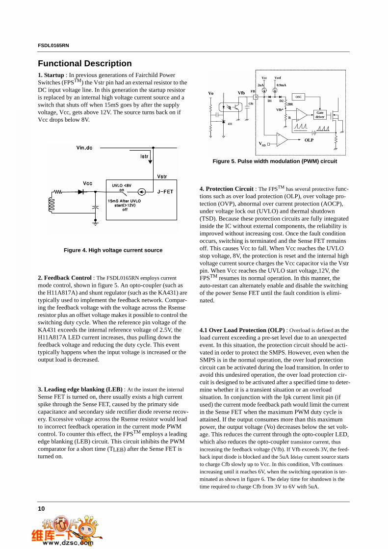
Functional Description1. Startup : In previous generations of Fairchild Power Switches (FPSTM) the Vstr pin had an external resistor to the DC input voltage line. In this generation the startup resistor is replaced by an internal high voltage current source and a switch that shuts off when 15mS goes by after the supply voltage, Vcc, gets above 12V. The source turns back on if Vcc drops below 8V.
Figure 4. High voltage current source
2. Feedback Control : The FSDL0165RN employs current mode control, shown in figure 5. An opto-coupler (such as the H11A817A) and shunt regulator (such as the KA431) are typically used to implement the feedback network. Compar-ing the feedback voltage with the voltage across the Rsense resistor plus an offset voltage makes it possible to control the switching duty cycle. When the reference pin voltage of the KA431 exceeds the internal reference voltage of 2.5V, the H11A817A LED current increases, thus pulling down the feedback voltage and reducing the duty cycle. This event typically happens when the input voltage is increased or the output load is decreased.
3. Leading edge blanking (LEB) : At the instant the internal Sense FET is turned on, there usually exists a high current spike through the Sense FET, caused by the primary side capacitance and secondary side rectifier diode reverse recov-ery. Excessive voltage across the Rsense resistor would lead to incorrect feedback operation in the current mode PWM control. To counter this effect, the FPSTM employs a leading edge blanking (LEB) circuit. This circuit inhibits the PWM comparator for a short time (TLEB) after the Sense FET is turned on.
Figure 5. Pulse width modulation (PWM) circuit
4. Protection Circuit : The FPSTM has several protective func-tions such as over load protection (OLP), over voltage pro-tection (OVP), abnormal over current protection (AOCP), under voltage lock out (UVLO) and thermal shutdown (TSD). Because these protection circuits are fully integrated inside the IC without external components, the reliability is improved without increasing cost. Once the fault condition occurs, switching is terminated and the Sense FET remains off. This causes Vcc to fall. When Vcc reaches the UVLO stop voltage, 8V, the protection is reset and the internal high voltage current source charges the Vcc capacitor via the Vstr pin. When Vcc reaches the UVLO start voltage,12V, the FPSTM resumes its normal operation. In this manner, the auto-restart can alternately enable and disable the switching of the power Sense FET until the fault condition is elimi-nated.
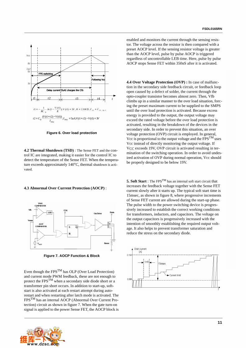
4.1 Over Load Protection (OLP) : Overload is defined as the load current exceeding a pre-set level due to an unexpected event. In this situation, the protection circuit should be acti-vated in order to protect the SMPS. However, even when the SMPS is in the normal operation, the over load protection circuit can be activated during the load transition. In order to avoid this undesired operation, the over load protection cir-cuit is designed to be activated after a specified time to deter-mine whether it is a transient situation or an overload situation. In conjunction with the Ipk current limit pin (if used) the current mode feedback path would limit the current in the Sense FET when the maximum PWM duty cycle is attained. If the output consumes more than this maximum power, the output voltage (Vo) decreases below the set volt-age. This reduces the current through the opto-coupler LED, which also reduces the opto-coupler transistor current, thus increasing the feedback voltage (Vfb). If Vfb exceeds 3V, the feed-back input diode is blocked and the 5uA Idelay current source starts to charge Cfb slowly up to Vcc. In this condition, Vfb continues increasing until it reaches 6V, when the switching operation is ter-minated as shown in figure 6. The delay time for shutdown is the time required to charge Cfb from 3V to 6V with 5uA.
Vin,dcVin,dcVin,dcVin,dc
VstrVstrVstrVstr
VccVccVccVcc
15mS After UVLO 15mS After UVLO 15mS After UVLO 15mS After UVLO start(>12V)start(>12V)start(>12V)start(>12V)
offoffoffoff
UVLO <8VUVLO <8VUVLO <8VUVLO <8Vonononon
IstrIstrIstrIstr
J-FETJ-FETJ-FETJ-FET
3 OSC
Vcc Vref
2uA 0.9mA
VSD
R
28R
FB
Gatedriver
OLP
D1 D2
Vfb*
Vfb
431
Cfb
Vo
FSDL0165RN
11
Figure 6. Over load protection
4.2 Thermal Shutdown (TSD) : The Sense FET and the con-trol IC are integrated, making it easier for the control IC to detect the temperature of the Sense FET. When the tempera-ture exceeds approximately 140°C, thermal shutdown is acti-vated.
4.3 Abnormal Over Current Protection (AOCP) :
Figure 7. AOCP Function & Block
Even though the FPSTM has OLP (Over Load Protection) and current mode PWM feedback, these are not enough to protect the FPSTM when a secondary side diode short or a transformer pin short occurs. In addition to start-up, soft-start is also activated at each restart attempt during auto-restart and when restarting after latch mode is activated. The FPSTM has an internal AOCP (Abnormal Over Current Pro-tection) circuit as shown in figure 7. When the gate turn-on signal is applied to the power Sense FET, the AOCP block is
enabled and monitors the current through the sensing resis-tor. The voltage across the resistor is then compared with a preset AOCP level. If the sensing resistor voltage is greater than the AOCP level, pulse by pulse AOCP is triggered regardless of uncontrollable LEB time. Here, pulse by pulse AOCP stops Sense FET within 350nS after it is activated.
4.4 Over Voltage Protection (OVP) : In case of malfunc-tion in the secondary side feedback circuit, or feedback loop open caused by a defect of solder, the current through the opto-coupler transistor becomes almost zero. Then, Vfb climbs up in a similar manner to the over load situation, forc-ing the preset maximum current to be supplied to the SMPS until the over load protection is activated. Because excess energy is provided to the output, the output voltage may exceed the rated voltage before the over load protection is activated, resulting in the breakdown of the devices in the secondary side. In order to prevent this situation, an over voltage protection (OVP) circuit is employed. In general, Vcc is proportional to the output voltage and the FPSTM uses Vcc instead of directly monitoring the output voltage. If VCC exceeds 19V, OVP circuit is activated resulting in ter-mination of the switching operation. In order to avoid undes-ired activation of OVP during normal operation, Vcc should be properly designed to be below 19V.
5. Soft Start : The FPSTM has an internal soft start circuit that increases the feedback voltage together with the Sense FET current slowly after it starts up. The typical soft start time is 15msec, as shown in figure 8, where progressive increments of Sense FET current are allowed during the start-up phase. The pulse width to the power switching device is progres-sively increased to establish the correct working conditions for transformers, inductors, and capacitors. The voltage on the output capacitors is progressively increased with the intention of smoothly establishing the required output volt-age. It also helps to prevent transformer saturation and reduce the stress on the secondary diode.
1t 2t 3t 4t t
3V
6V
Vcc
8V
Delay current (5uA) charges the CfbDelay current (5uA) charges the CfbDelay current (5uA) charges the CfbDelay current (5uA) charges the Cfb
FPS switchingFPS switchingFPS switchingFPS switching
OLP
Following VccFollowing VccFollowing VccFollowing Vcc
2._,8.2,3)1();)1(1(11 figfbfbfb
CCKRVtVRtVIn
RCt =Ω==−−=
VtVttVuAII
tVttVCt delaydelay
fb 3)1()21(,5;))1()21((2 =−+=−+=
R
S Q
Vsense
Vfb
Out Driver
Rsense
CLKDrain
VAOCP
PWMCOMPARATOR
AOCPCOMPARATOR
LEB
1mS15steps
Current limit
0.98A
2.15A
t
Drain current[A]
FSDL0165RN
12
Figure 8. Soft Start Function
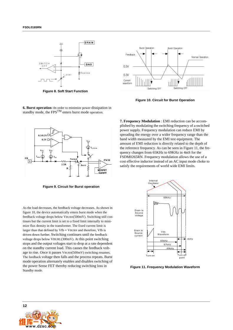
6. Burst operation :In order to minimize power dissipation in standby mode, the FPSTM enters burst mode operation.
Figure 9. Circuit for Burst operation
As the load decreases, the feedback voltage decreases. As shown in figure 10, the device automatically enters burst mode when the feedback voltage drops below VBURH(500mV). Switching still con-tinues but the current limit is set to a fixed limit internally to mini-mize flux density in the transformer. The fixed current limit is larger than that defined by Vfb = VBURH and therefore, Vfb is driven down further. Switching continues until the feedback voltage drops below VBURL(300mV). At this point switching stops and the output voltages start to drop at a rate dependent on the standby current load. This causes the feedback volt-age to rise. Once it passes VBURH(500mV) switching resumes. The feedback voltage then falls and the process repeats. Burst mode operation alternately enables and disables switching of the power Sense FET thereby reducing switching loss in Standby mode.
Figure 10. Circuit for Burst Operation
7. Frequency Modulation : EMI reduction can be accom-plished by modulating the switching frequency of a switched power supply. Frequency modulation can reduce EMI by spreading the energy over a wider frequency range than the band width measured by the EMI test equipment. The amount of EMI reduction is directly related to the depth of the reference frequency. As can be seen in Figure 11, the fre-quency changes from 65KHz to 69KHz in 4mS for the FSDM0265RN. Frequency modulation allows the use of a cost effective inductor instead of an AC input mode choke to satisfy the requirements of world wide EMI limits.
Figure 11. Frequency Modulation Waveform
D R A IND R A IND R A IND R A IN
G N DG N DG N DG N D
R s e n s eI_ o v e r
S W IT C H O F F
5 V
3
Vcc Vcc
Idelay IFB
R2.5R
FB
0.3/0.5V
PWM
+
-
0.5VVcc
IB_PEAK
Burst
Normal
MOSFET MOSFET MOSFET MOSFET CurrentCurrentCurrentCurrent
0.5V
Switching OFF
Current waveform
Burst Operation
Normal OperationFeedback
0.3V
Burst Operation
Switching OFF
69kHz
69kHz
67kH z
65kHz4kHz
Turn-on Turn-offpoint
InternalO scillator
Drain toSourcevoltage
V dsW aveform
Drain toSourcecurrent
FSDL0165RN
13
Figure 12. KA5-series FPSTM Full Range EMI scan(67KHz, no Frequency Modulation) with DVD Player SET
Figure 13. FSDX-series FPSTM Full Range EMI Scan (67KHz, with Frequency Modulation) with DVD Player SET
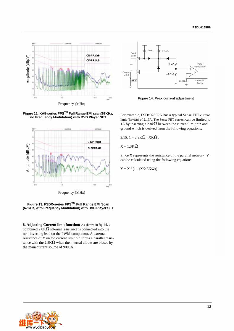
8. Adjusting Current limit function: As shown in fig 14, a combined 2.8KΩ internal resistance is connected into the non-inverting lead on the PWM comparator. A external resistance of Y on the current limit pin forms a parallel resis-tance with the 2.8KΩ when the internal diodes are biased by the main current source of 900uA.
Figure 14. Peak current adjustment
For example, FSDx0265RN has a typical Sense FET current limit (IOVER) of 2.15A. The Sense FET current can be limited to 1A by inserting a 2.8kΩ between the current limit pin and ground which is derived from the following equations:
2.15: 1 = 2.8KΩ : XKΩ ,
X = 1.3KΩ,
Since X represents the resistance of the parallel network, Y can be calculated using the following equation:
Y = X / (1 - (X/2.8KΩ))
Frequency (MHz)
Am
plitu
de (d
BµV
) CISPR2QB
CISPR2AB
Frequency (MHz)
Am
plitu
de (d
BµV
) CISPR2QB
CISPR2AB
3
4
PWM comparator
SenseFETSense
ΩK2
ΩK8.0
ΩAK
900uA5uA
Rsense
FeedBack
CurrentLimit
FSDL0165RN
14
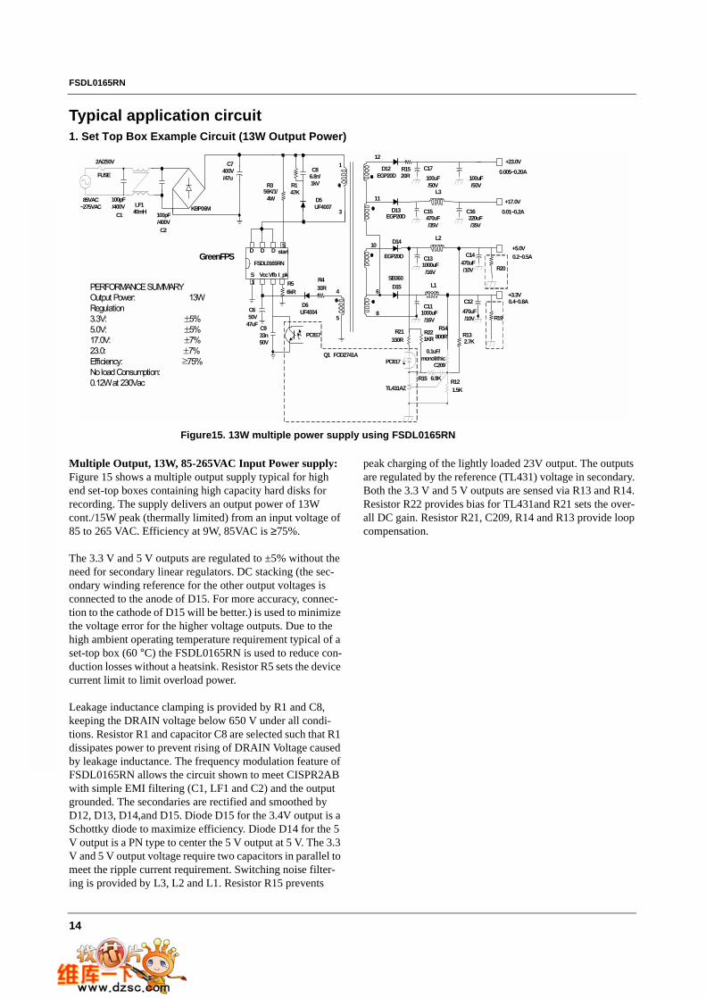
Typical application circuit 1. Set Top Box Example Circuit (13W Output Power)
FSDL0165RN
1
5D D D
S VccVfb
C7400V/47u
D5UF4007
R147K
D6UF4004
C933n50V
I_pk
start
C86.8n/1kV
R430R
C650V
47uF
D15SB360
D14
D13EGP20D
D12
PC817
FOD2741A
L1
L2
L3
C11C12
+3.3V
+5.0V
+17.0V
+23.0V
0.4~0.8A
0.2~0.5A
0.01~0.2A
0.005~0.20A
C13
C15
C17
C16
C14
1000uF/16V
470uF/10V
1000uF/16V
470uF/10V
470uF/35V
220uF/35V
100uF/50V
100uF/50V
R21 R14R13
R15
330R 800R
6.9K R12
2.7K
1.5K
C209
0.1uF/monolithic
LF140mH KBP06M
100pF/400V
100pF/400VC2
C1
2A/250V
FUSE
85VAC~275VAC
56K/1/4W
R3
Q1
R19
R20
PC817
TL431AZ
EGP20D
EGP20D
1
3
4
58
6
10
11
12
PERFORMANCE SUMMARYOutput Power: 13WRegulation3.3V: ±5%5.0V: ±5%17.0V: ±7%23.0: ±7%Efficiency: ≥75%No load Consumption:0.12W at 230Vac
GreenFPS
R56kR
R1520R
R221KR
Figure15. 13W multiple power supply using FSDL0165RN
Multiple Output, 13W, 85-265VAC Input Power supply: Figure 15 shows a multiple output supply typical for high end set-top boxes containing high capacity hard disks for recording. The supply delivers an output power of 13W cont./15W peak (thermally limited) from an input voltage of 85 to 265 VAC. Efficiency at 9W, 85VAC is ≥75%.
The 3.3 V and 5 V outputs are regulated to ±5% without the need for secondary linear regulators. DC stacking (the sec-ondary winding reference for the other output voltages is connected to the anode of D15. For more accuracy, connec-tion to the cathode of D15 will be better.) is used to minimize the voltage error for the higher voltage outputs. Due to the high ambient operating temperature requirement typical of a set-top box (60 °C) the FSDL0165RN is used to reduce con-duction losses without a heatsink. Resistor R5 sets the device current limit to limit overload power.
Leakage inductance clamping is provided by R1 and C8, keeping the DRAIN voltage below 650 V under all condi-tions. Resistor R1 and capacitor C8 are selected such that R1 dissipates power to prevent rising of DRAIN Voltage caused by leakage inductance. The frequency modulation feature of FSDL0165RN allows the circuit shown to meet CISPR2AB with simple EMI filtering (C1, LF1 and C2) and the output grounded. The secondaries are rectified and smoothed by D12, D13, D14,and D15. Diode D15 for the 3.4V output is a Schottky diode to maximize efficiency. Diode D14 for the 5 V output is a PN type to center the 5 V output at 5 V. The 3.3 V and 5 V output voltage require two capacitors in parallel to meet the ripple current requirement. Switching noise filter-ing is provided by L3, L2 and L1. Resistor R15 prevents
peak charging of the lightly loaded 23V output. The outputs are regulated by the reference (TL431) voltage in secondary. Both the 3.3 V and 5 V outputs are sensed via R13 and R14. Resistor R22 provides bias for TL431and R21 sets the over-all DC gain. Resistor R21, C209, R14 and R13 provide loop compensation.
FSDL0165RN
15
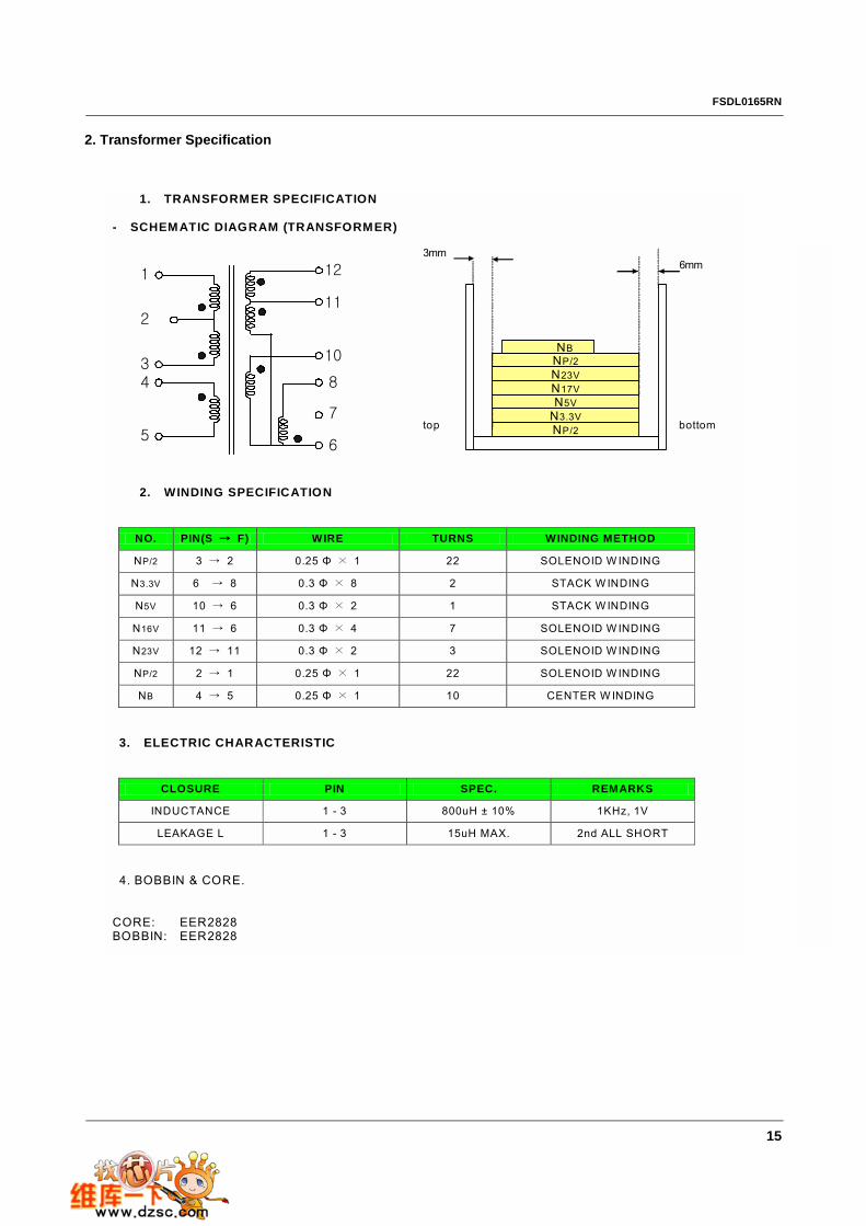
2. Transformer Specification
1. TRANSFORMER SPECIFICATION - SCHEMATIC DIAGRAM (TRANSFORMER)
2. WINDING SPECIFICATION
NO. PIN(S →→→→ F) WIRE TURNS WINDING METHOD
NP/2 3 → 2 0.25 Φ × 1 22 SOLENOID W INDING
N3.3V 6 → 8 0.3 Φ × 8 2 STACK W INDING
N5V 10 → 6 0.3 Φ × 2 1 STACK W INDING
N16V 11 → 6 0.3 Φ × 4 7 SOLENOID W INDING
N23V 12 → 11 0.3 Φ × 2 3 SOLENOID W INDING
NP/2 2 → 1 0.25 Φ × 1 22 SOLENOID W INDING
NB 4 → 5 0.25 Φ × 1 10 CENTER W INDING
3. ELECTRIC CHARACTERISTIC
CLOSURE PIN SPEC. REMARKS
INDUCTANCE 1 - 3 800uH ± 10% 1KHz, 1V
LEAKAGE L 1 - 3 15uH MAX. 2nd ALL SHORT
4. BOBBIN & CORE. CORE: EER2828 BOBBIN: EER2828
NP/2N3.3V
NP/2 NB
3mm6mm
bottom top
N5V
N23VN17V
1
2
34
56
7
8
10
11
12
FSDL0165RN
16
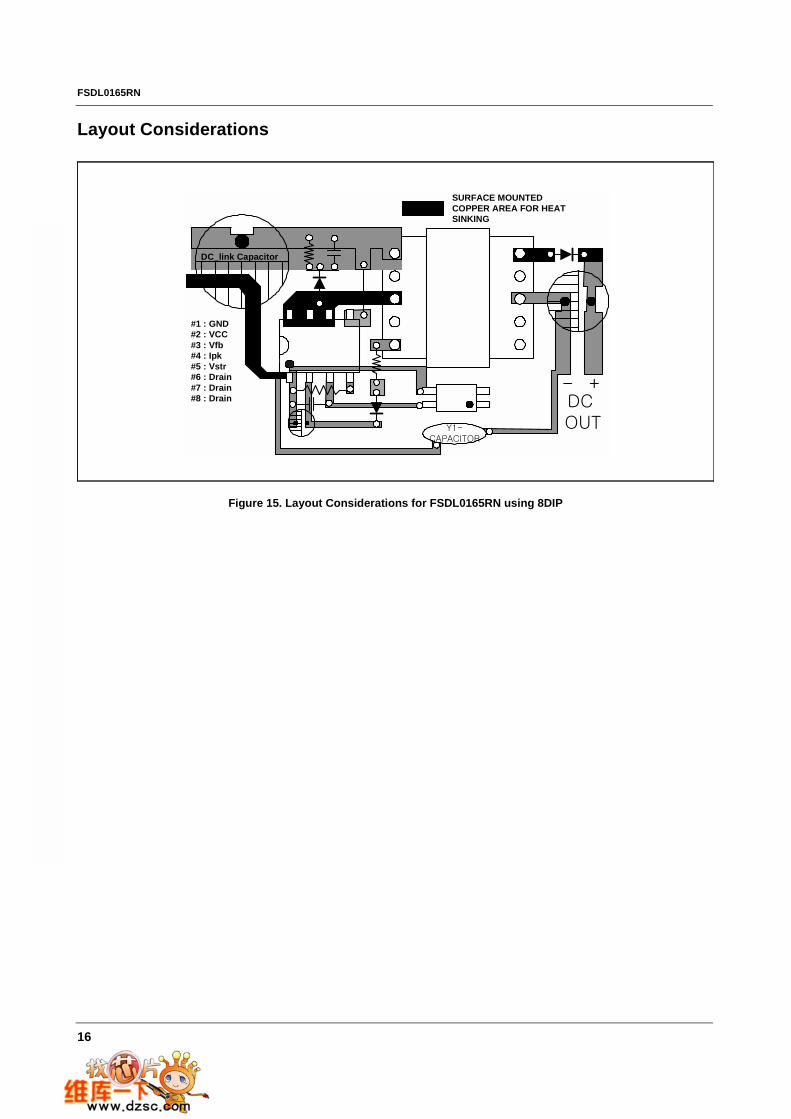
Layout Considerations
Figure 15. Layout Considerations for FSDL0165RN using 8DIP
#1 : GND#2 : VCC#3 : Vfb#4 : Ipk#5 : Vstr#6 : Drain#7 : Drain#8 : Drain
SURFACE MOUNTEDCOPPER AREA FOR HEATSINKING
Y1-CAPACITOR
+-DC OUT
DC_link Capacitor
FSDL0165RN
17
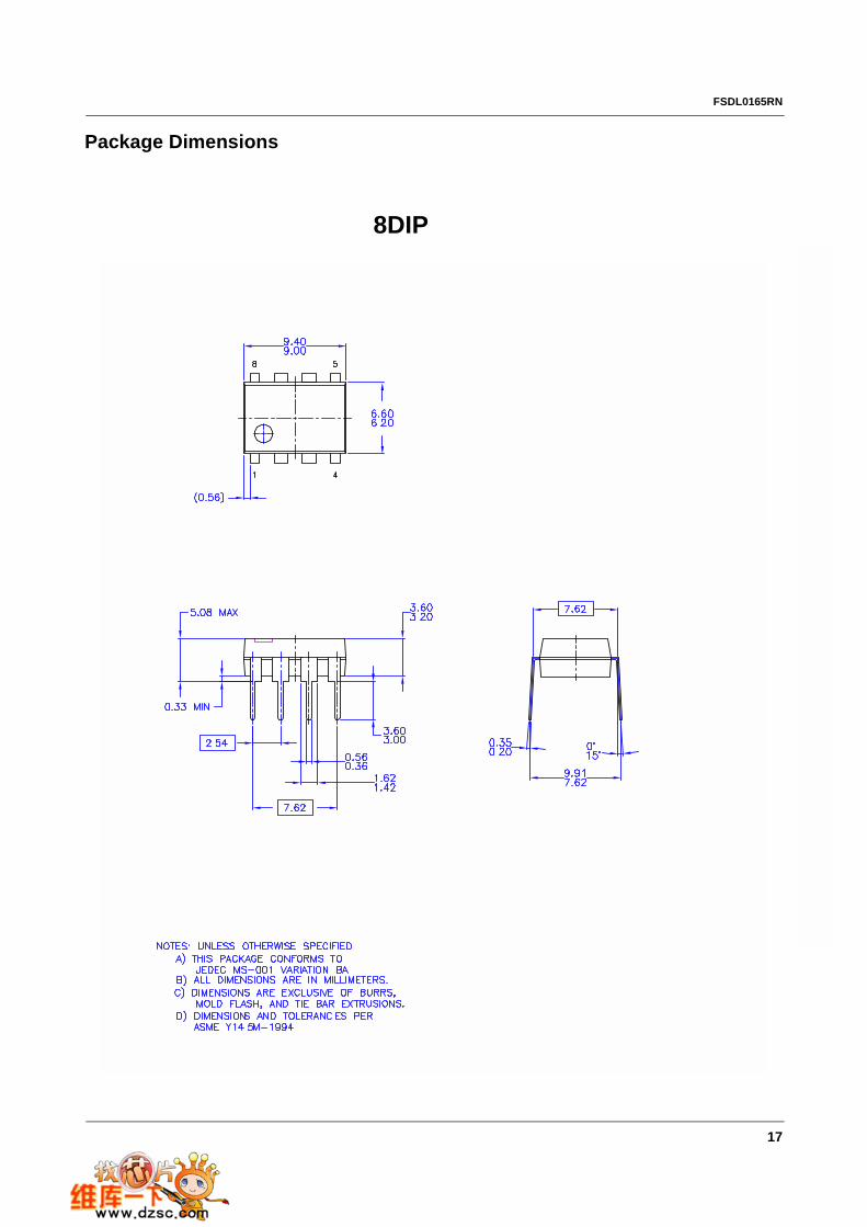
Package Dimensions
8DIP
FSDL0165RN
18
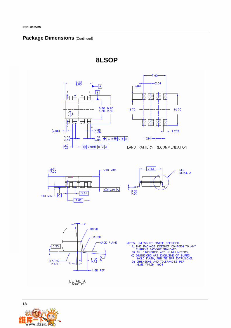
Package Dimensions (Continued)
8LSOP

FSDL0165RN
19
Ordering InformationProduct Number Package Marking Code BVDSS FOSC RDS(on)
FSDL0165RN 8DIP DL0165R 650V 50KHz 8.0ΩFSDL0165RL 8LSOP DL0165R 650V 50KHz 8.0Ω
FSDL0165RN
6/17/04 0.0m 001 2004 Fairchild Semiconductor Corporation
LIFE SUPPORT POLICY FAIRCHILDS PRODUCTS ARE NOT AUTHORIZED FOR USE AS CRITICAL COMPONENTS IN LIFE SUPPORT DEVICES OR SYSTEMS WITHOUT THE EXPRESS WRITTEN APPROVAL OF THE PRESIDENT OF FAIRCHILD SEMICONDUCTOR CORPORATION. As used herein:
1. Life support devices or systems are devices or systems which, (a) are intended for surgical implant into the body, or (b) support or sustain life, and (c) whose failure to perform when properly used in accordance with instructions for use provided in the labeling, can be reasonably expected to result in a significant injury of the user.
2. A critical component in any component of a life support device or system whose failure to perform can be reasonably expected to cause the failure of the life support device or system, or to affect its safety or effectiveness.
www.fairchildsemi.com
DISCLAIMERFAIRCHILD SEMICONDUCTOR RESERVES THE RIGHT TO MAKE CHANGES WITHOUT FURTHER NOTICE TO ANY PRODUCTS HEREIN TO IMPROVE RELIABILITY, FUNCTION OR DESIGN. FAIRCHILD DOES NOT ASSUME ANY LIABILITY ARISING OUT OF THE APPLICATION OR USE OF ANY PRODUCT OR CIRCUIT DESCRIBED HEREIN; NEITHER DOES IT CONVEY ANY LICENSE UNDER ITS PATENT RIGHTS, NOR THE RIGHTS OF OTHERS.