Embed Size (px)
Citation preview
Fully-Integrated, Power-Efficient Regulator andBandgap Circuits for Wireless-Powered Biomedical
ApplicationsMeysam Zargham, P. Glenn Gulak
School of Electrical and Computer EngineeringUniversity of Toronto
Email: {zarghamm,gulak}@eecg.toronto.edu
Abstract—Design and Measurement results are presented fora fully integrated, linear, low-dropout regulator with a quiescentcurrent of 12µA. The regulator is able to recover from fullload steps with less than 10% change in the regulated voltageand in less than 2µs. The regulator reference is generated bya curvature-compensated bandgap reference. The reference usesonly 9.8µA and has a temperature coefficient of 2.95-ppm/◦C andcan tolerate a wide range of input voltages from 3.2V to 8V with aline regulation of 160µV/V. These blocks are fabricated in 0.13µmCMOS process, do not require off-chip components and targetpower harvesting biomedical and lab-on-a-chip applications thatrequire up to 5mA of current from a 3.3V supply.
I. INTRODUCTION
Wireless power delivery is becoming increasingly importantfor implantable microelectronics devices (IMD) and lab-on-chip (LoC) applications that require measurement or sensing ofbiological phenomenon. In these scenarios the use of batteriesis restricted due to their size, cost, lifetime and packagingissues. Within this domain, near-field inductive coupling is oneof the most practical ways of transmitting data and energy toimplantable devices. Examples of such sensors are bacteriaidentification circuits or neural implants. In such systemsthe circuits contained in the IMD or the LoC are remotelypowered by means of two coupled inductors and a poweramplifier operating at a fixed carrier frequency. Employingthis transmitted energy at the receiver requires a rectifier,regulator and a bandgap voltage reference to deliver stable,load-independent voltage to the circuit. It is important forthese power management units to be low-power, low-costand add as little 1/f noise as possible to the system. It isalso highly desirable to fully integrate the power receivercircuits and the coil on the CMOS substrate. Aside from theobvious reduction in size compared to typical implants thatare already in use today, a wireless power transfer (WPT)receiver integrated on a single CMOS substrate is protectedfrom the outside environment through a passivation layer,while access to sensor electrodes would be granted throughselected passivation openings across the die. The later propertyis especially beneficial in accommodating applications thatinvolve liquid samples. As a result the die would be readilymass producible. The power efficiency of the link is given
below:
ηtotal = ηPA × ηcoupling × ηrectifier × ηregulator (1)
But, due to the limited size of an on-chip receiver coil, theelectrical properties of the Si substrate and the conductivemedia between the TX and RX coils, the coupling efficiency(ηcoupling) suffers from low efficiency [1]. Therefore it iscritical for the regulator to provide high efficiency. In additionto this, due to low coupling efficiency, the range of deliveredpower in these systems is between hundreds of µW to a fewmW [1]. A great deal of attention in the literature has beendevoted to integrated CMOS regulators that are optimized forpower delivery in the 100’s of mW and greater. Yet, none ofthe literature surveyed is optimized for high efficiency andaccuracy in the mW regime required for a wide range ofbiomedical applications. Optimizing the power delivery unitfor this power range presents a new set of tradeoffs and circuitdesign opportunities. This paper presents a power-efficient,low-complexity regulator and bandgap circuit, requiring noexternal components that targets biomedical sensor measure-ment applications that need a few mW of wireless power. Theremainder of the paper is organized as follows. In sectionII,III, we introduce the bangap circuit and its measurementresults. Section IV discusses the regulator circuit. Finally thelast section concludes the paper.
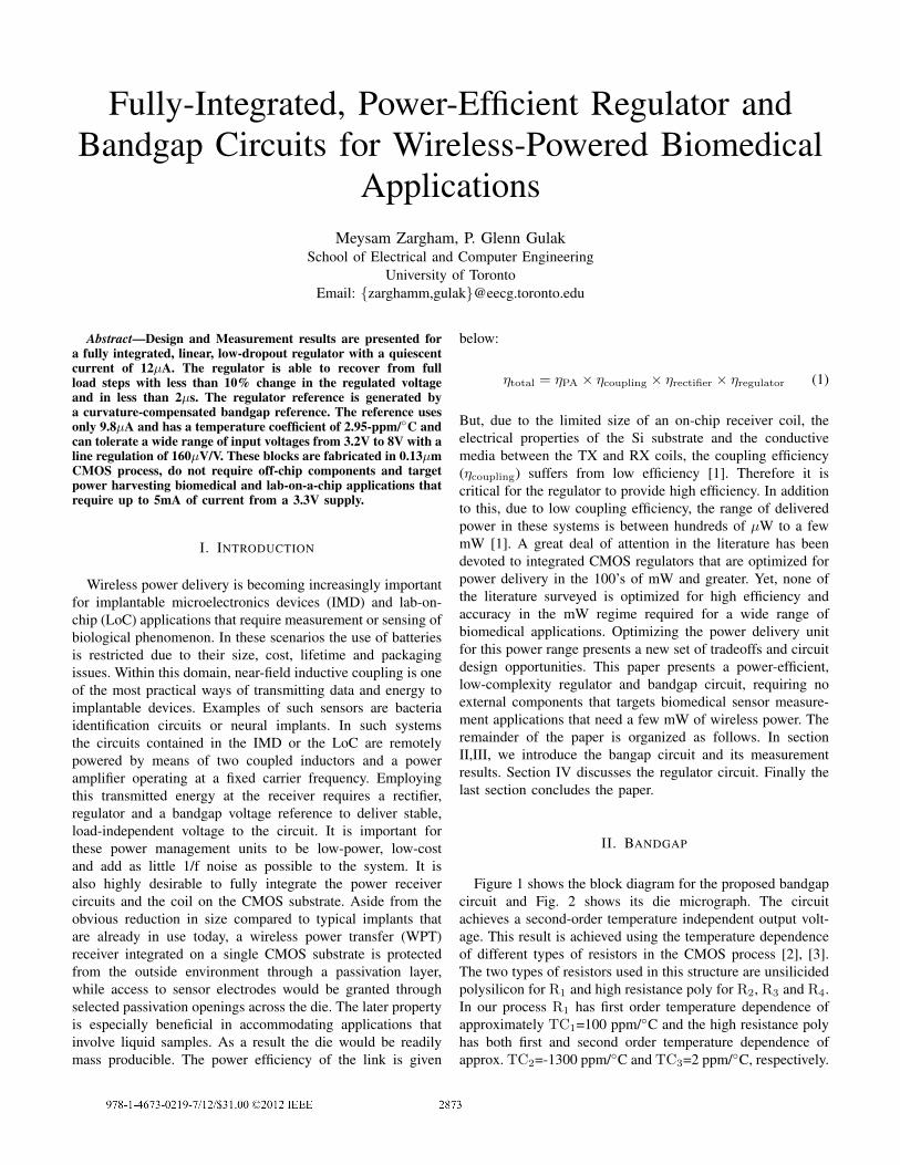
II. BANDGAP
Figure 1 shows the block diagram for the proposed bandgapcircuit and Fig. 2 shows its die micrograph. The circuitachieves a second-order temperature independent output volt-age. This result is achieved using the temperature dependenceof different types of resistors in the CMOS process [2], [3].The two types of resistors used in this structure are unsilicidedpolysilicon for R1 and high resistance poly for R2, R3 and R4.In our process R1 has first order temperature dependence ofapproximately TC1=100 ppm/◦C and the high resistance polyhas both first and second order temperature dependence ofapprox. TC2=-1300 ppm/◦C and TC3=2 ppm/◦C, respectively.
The output voltage using different resistances is:
Vbg = VEB(Q1)(T) +R3
R2ln(N)VT +
R1
R2× (2)
ln(N)(1 + TC1 × T)
1 + TC2 × T + TC3 × T2.
Where T is the temperature, VEB(Q1)(T) is the emitter basevoltage of Q1, N is the ratio between the emitter areas of Q4
and Q1 and VT is the thermal voltage. Now by applying Taylorseries at room temperature around T0 = 300◦K and replacingVEB(Q1)(T) from [4] the output voltage (2) becomes:
Vb2
Vb3
Vb2
Vb3
+ -
Amplifier
Amplifier Bandgap Startup
M1M2M3M4
M5M6M7M8
R1
R3
R2
R4M11 M12
M13M14M15
Cc
M16 M9
M10
Q1Q2Q3 Q4
Vbg
×N×N
M17
M18
Fig. 1. Proposed bandgap circuit.
Fig. 2. Die micrograph of the proposed bandgap in 0.13µm CMOS process.
Vbg 'α0 +
(R1 + R3
R2-α1
)VT ln(N) + (3)(
R1(TC1-TC2)
R2-α2
)T ·VT ln(N)−(
R1 · TC3
R2-α2
3T0
)T2 ·VT ln(N) .
Where αi are positive process dependant constants, hence byproperly choosing, R2 and R3 we completely eliminate firstand second order temperature dependent terms and reducethe cubic term in the output voltage and R4 improves thecurrent mirror matching. In order for the above assumptionsto hold we require a high-gain, low-offset amplifier and
matched current sources. In addition to these, since theresistance seen by the current mirrors M7 and M8 is now afunction of temperature, they require high output impedance.The proposed amplifier is self-biased using an internalpositive feedback loop. As a result, the bias current ofthe amplifier does not change with Vdd variations. Thepositive feedback loop has a loop gain of approximatelygm15/(2gm14) which is designed to be less than one. Thisvalue is further reduced by a weak negative feedback loopthrough M17, M18 and M10. The gain of the amplifier isAv = gm11 × (ro14||ro11)× gm15 × (ro15||1/gm16)=60dB.where gm is the transconductance of the transistors andro denotes the output impedance of the transistors. Theamplifier also has positive and negative external feedbackloops however due to the small resistance seen at the emitterof Q1 compared to R2 resistor, the overall feedback isalways negative at low frequencies. The high frequencystability of the circuit can easily be achieved using Millercompensation. In order to improve current matching, reducenoise and increase the output impedance of the top currentmirrors, we are using very long channel lengths for the toppMOS transistors and average W/L ratios for the cascadetransistors. The input differential pair was realized usingpMOS transistors to eliminate the body effect and decreasethe 1/f noise. They also occupy large area and have largewidths to reduce offset and noise and improve gm efficiency.The pnp transistors are implemented using the parasitic BJTsin the CMOS process. The role of Q2 and Q3 is to cancel thebase current of Q1 and Q4 [10]. In order to reduce the powerconsumption of the bandgap we did not use the conventionalstartup circuits. The current consumption of the conventionalstartup circuits is a function input voltage and increases asthe vdd is raised. The startup circuit in Fig. 1 uses no currentduring the operation of the bandgap. The circuit was testedunder a wide variety of startup conditions and it was alwaysable to successfully produce the correct voltage.
III. BANDGAP MEASUREMENT RESULTS
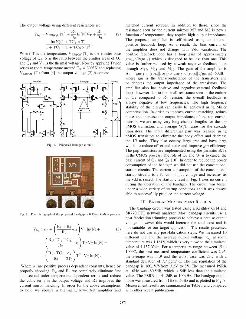
The bandgap circuit was tested using a Keithley 6514 andSR770 FFT network analyzer. Most bandgap circuits use apost-fabrication trimming process to achieve a precise outputvoltage; however this would increase the total cost and isnot suitable for our target application. The results presentedhere do not use any post-fabrication steps. We measured 10different die and the average output voltage Vbg at roomtemperature was 1.161V, which is very close to the simulatedvalue of 1.157 Volts. For a temperature range between -5 to100◦C, the best measured temperature coefficient was 2.95,the average was 11.9 and the worst case was 23.7 with astandard deviation of 7.7 ppm/◦C. The line regulation of thebandgap is 160µV/Vfrom 3.2V to 8V. The measured PSRRat 10Hz was -80.5dB, which is 5dB less than the simulatedvalue. The PSRR is -41.2dB at 100kHz. The bandgap outputnoise was measured from 1Hz to 50Hz and is plotted in Fig. 3.Measurement results are summarized in Table I and comparedwith other recent publications.
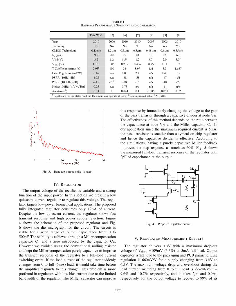
TABLE IBANDGAP PERFORMANCE SUMMARY AND COMPARISON
This Work [5] [6] [7] [8] [3] [9]
Year 2010 2000 2010 2010 2007 2003 2010Trimming No No No No No Yes YesCMOS Technology 0.13µm 1.2µm 0.5µm 0.5µm 0.18µm 0.6µm 0.35µmIQ(µA) 9.8 500 28 40 10.1 23 6.6Vdd(V) 3.2 1.2 1.57 1.2 3.07 2.0 3.07
Vout(V) 1.161 1.05 0.235 0.486 0.75 1.14 1.2T-Coefficientppm/◦C 2.958 100 34 8.98 131 5.3 12.67Line Regulation(mV/V) 0.16 n/a 0.05 2.4 n/a 1.43 1.8PSRR (10Hz)[dB] -80.5 n/a -68 -58 n/a -47 -51PSRR (100kHz)[dB] -41.2 -209 -30 -15 n/a -10 -28Noise(100Hz)[µV/
√Hz] 0.75 n/a 0.75 n/a n/a 1 n/a
Area(mm2) 0.03 1 0.044 0.1 0.085 0.057 0.027Results are for the stated Vdd but the circuit can operate at lower. 8Best measured value. 9At 1kHz.
Fig. 3. Bandgap output noise voltage.
IV. REGULATOR
The output voltage of the rectifier is variable and a strongfunction of the input power. In this section we present a lowquiescent current regulator to regulate this voltage. The regu-lator targets low-power biomedical applications. The proposedfully integrated regulator consumes only 12µA of current.Despite the low quiescent current, the regulator shows fasttransient response and high power supply rejection. Figure4 shows the schematic of the proposed regulator and Fig.6 shows the die micrograph for the circuit. The circuit isstable for a wide range of output capacitance from 0 to500pF. The stability is achieved through a Miller compensationcapacitor Cc and a zero introduced by the capacitor CZ.However we avoided using the conventional nulling resistorand kept the Miller compensation purely capacitive to improvethe transient response of the regulator to a full-load currentswitching event. If the load current of the regulator suddenlychanges from 0 to full (5mA) load, it would take time beforethe amplifier responds to this change. This problem is moreprofound in regulators with low bias current due to the limitedbandwidth of the regulator. The Miller capacitor can improve
this response by immediately changing the voltage at the gateof the pass transistor through a capacitive divider at node VG.The effectiveness of this method depends on the ratio betweenthe capacitance at node VG and the Miller capacitor Cc. Inour application since the maximum required current is 5mA,the pass transistor is smaller than a typical on-chip regulatorand hence the capacitive divider is effective. According tothe simulations, having a purely capacitive Miller feedbackimproves the step response as much as 60%. Fig. 5 showsthe measured full-load transient response of the regulator with2pF of capacitance at the output.
Vb1
Cc
Vbg
Cz
Co
MP
CP
VG
VREG
Fig. 4. Proposed regulator circuit.
V. REGULATOR MEASUREMENT RESULTS
The regulator delivers 3.3V with a maximum drop-outvoltage of Vdrop =109mV (3.3%) at 5mA full load. Outputcapacitor is 2pF due to the packaging and PCB parasitic. Lineregulation is 660µV/V for a supply changing from 3.4V to6.5V. The maximum voltage drop and overshoot during theload current switching from 0 to full load is ∆Vout/Vout =9.6% and 10.7% respectively, and it takes 2µs and 0.9µs,respectively, for the output voltage to recover to 99% of its
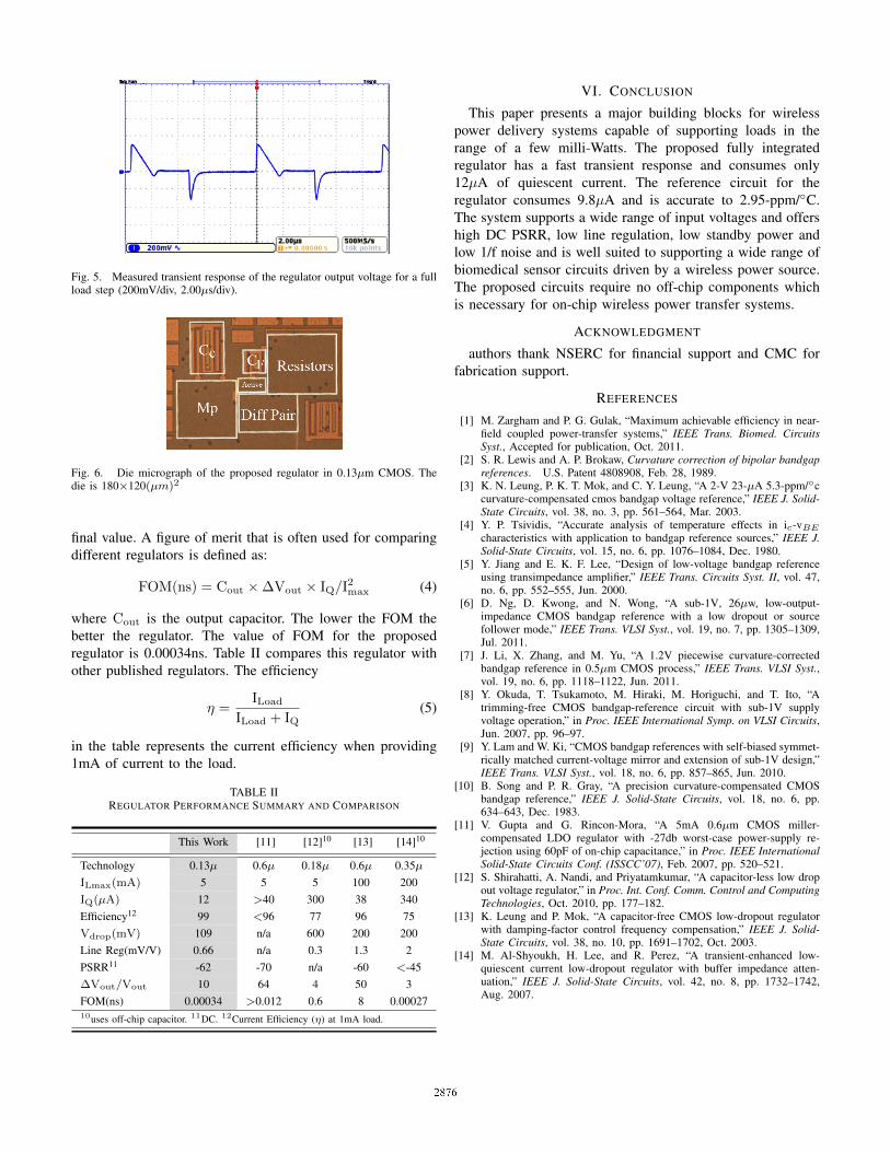
Fig. 5. Measured transient response of the regulator output voltage for a fullload step (200mV/div, 2.00µs/div).
Fig. 6. Die micrograph of the proposed regulator in 0.13µm CMOS. Thedie is 180×120(µm)2
final value. A figure of merit that is often used for comparingdifferent regulators is defined as:
FOM(ns) = Cout ×∆Vout × IQ/I2max (4)
where Cout is the output capacitor. The lower the FOM thebetter the regulator. The value of FOM for the proposedregulator is 0.00034ns. Table II compares this regulator withother published regulators. The efficiency
η =ILoad
ILoad + IQ(5)
in the table represents the current efficiency when providing1mA of current to the load.
TABLE IIREGULATOR PERFORMANCE SUMMARY AND COMPARISON
This Work [11] [12]10 [13] [14]10
Technology 0.13µ 0.6µ 0.18µ 0.6µ 0.35µILmax(mA) 5 5 5 100 200IQ(µA) 12 >40 300 38 340Efficiency12 99 <96 77 96 75Vdrop(mV) 109 n/a 600 200 200Line Reg(mV/V) 0.66 n/a 0.3 1.3 2PSRR11 -62 -70 n/a -60 <-45∆Vout/Vout 10 64 4 50 3FOM(ns) 0.00034 >0.012 0.6 8 0.0002710uses off-chip capacitor. 11DC. 12Current Efficiency (η) at 1mA load.
VI. CONCLUSION
This paper presents a major building blocks for wirelesspower delivery systems capable of supporting loads in therange of a few milli-Watts. The proposed fully integratedregulator has a fast transient response and consumes only12µA of quiescent current. The reference circuit for theregulator consumes 9.8µA and is accurate to 2.95-ppm/◦C.The system supports a wide range of input voltages and offershigh DC PSRR, low line regulation, low standby power andlow 1/f noise and is well suited to supporting a wide range ofbiomedical sensor circuits driven by a wireless power source.The proposed circuits require no off-chip components whichis necessary for on-chip wireless power transfer systems.
ACKNOWLEDGMENT
authors thank NSERC for financial support and CMC forfabrication support.
REFERENCES
[1] M. Zargham and P. G. Gulak, “Maximum achievable efficiency in near-field coupled power-transfer systems,” IEEE Trans. Biomed. CircuitsSyst., Accepted for publication, Oct. 2011.
[2] S. R. Lewis and A. P. Brokaw, Curvature correction of bipolar bandgapreferences. U.S. Patent 4808908, Feb. 28, 1989.
[3] K. N. Leung, P. K. T. Mok, and C. Y. Leung, “A 2-V 23-µA 5.3-ppm/◦ccurvature-compensated cmos bandgap voltage reference,” IEEE J. Solid-State Circuits, vol. 38, no. 3, pp. 561–564, Mar. 2003.
[4] Y. P. Tsividis, “Accurate analysis of temperature effects in ic-vBE
characteristics with application to bandgap reference sources,” IEEE J.Solid-State Circuits, vol. 15, no. 6, pp. 1076–1084, Dec. 1980.
[5] Y. Jiang and E. K. F. Lee, “Design of low-voltage bandgap referenceusing transimpedance amplifier,” IEEE Trans. Circuits Syst. II, vol. 47,no. 6, pp. 552–555, Jun. 2000.
[6] D. Ng, D. Kwong, and N. Wong, “A sub-1V, 26µw, low-output-impedance CMOS bandgap reference with a low dropout or sourcefollower mode,” IEEE Trans. VLSI Syst., vol. 19, no. 7, pp. 1305–1309,Jul. 2011.
[7] J. Li, X. Zhang, and M. Yu, “A 1.2V piecewise curvature-correctedbandgap reference in 0.5µm CMOS process,” IEEE Trans. VLSI Syst.,vol. 19, no. 6, pp. 1118–1122, Jun. 2011.
[8] Y. Okuda, T. Tsukamoto, M. Hiraki, M. Horiguchi, and T. Ito, “Atrimming-free CMOS bandgap-reference circuit with sub-1V supplyvoltage operation,” in Proc. IEEE International Symp. on VLSI Circuits,Jun. 2007, pp. 96–97.
[9] Y. Lam and W. Ki, “CMOS bandgap references with self-biased symmet-rically matched current-voltage mirror and extension of sub-1V design,”IEEE Trans. VLSI Syst., vol. 18, no. 6, pp. 857–865, Jun. 2010.
[10] B. Song and P. R. Gray, “A precision curvature-compensated CMOSbandgap reference,” IEEE J. Solid-State Circuits, vol. 18, no. 6, pp.634–643, Dec. 1983.
[11] V. Gupta and G. Rincon-Mora, “A 5mA 0.6µm CMOS miller-compensated LDO regulator with -27db worst-case power-supply re-jection using 60pF of on-chip capacitance,” in Proc. IEEE InternationalSolid-State Circuits Conf. (ISSCC’07), Feb. 2007, pp. 520–521.
[12] S. Shirahatti, A. Nandi, and Priyatamkumar, “A capacitor-less low dropout voltage regulator,” in Proc. Int. Conf. Comm. Control and ComputingTechnologies, Oct. 2010, pp. 177–182.
[13] K. Leung and P. Mok, “A capacitor-free CMOS low-dropout regulatorwith damping-factor control frequency compensation,” IEEE J. Solid-State Circuits, vol. 38, no. 10, pp. 1691–1702, Oct. 2003.
[14] M. Al-Shyoukh, H. Lee, and R. Perez, “A transient-enhanced low-quiescent current low-dropout regulator with buffer impedance atten-uation,” IEEE J. Solid-State Circuits, vol. 42, no. 8, pp. 1732–1742,Aug. 2007.