Embed Size (px)
Citation preview
EPC – EFFICIENT POWER CONVERSION CORPORATION | WWW.EPC-CO.COM | COPYRIGHT 2011 | | PAGE 1
APPLICATION NOTE: AN002 GaN Power Transistors
StructureA device’s cost effectiveness starts with lever-aging existing production infrastructure. EPC’s process begins with silicon wafers. Utiilizing ex-isting silicon processing equipment, a thin layer of Aluminum Nitride (AlN) is grown on the Silicon to isolate the device structure from the Substrate. The isolation layer for 200 V and below devices is 300 V. On top of this, a thick layer of highly resis-tive Gallium Nitride is grown. This layer provides a foundation on which to build the GaN transis-tor. An electron generating material is applied to the GaN. This layer creates a GaN layer with
an abundance of electrons just below it that is highly conductive. Further processing forms a depletion region under the gate. To enhance the transistor, a positive voltage is applied to the gate in the same manner as turning on an n-channel, enhancement mode power MOSFET. A cross sec-tion of this structure is depicted in figure 1. This structure is repeated many times to form a power device. The end result is a fundamentally simple, elegant, cost effective solution for power switch-ing. This device behaves similarly to Silicon MOS-FETs with some exceptions that will be explained in the following sections.
OperationEPC’s GaN transistors behave very similarly to Silicon Power MOSFETs. A positive bias on the gate relative to the source causes a field effect which attracts electrons that complete a bidirec-tional channel between the drain and the source. Since the electrons are pooled, as opposed to being loosely trapped in a lattice, the resistance of this channel is quite low. When the bias is re-moved from the gate, the electrons under it are dispersed into the GaN, recreating the depletion region, and once again, giving it the capability to block voltage.
Fundamentals of Gallium Nitride Power TransistorsStephen L. Colino and Robert A. Beach, Ph.D.
The basic requirements for power semiconductors are effciency, reliability, con-trollability, and cost effectiveness. High frequency capability adds further value in size and transient response in regulators, and fidelity in class D amplifiers. With-out effciency and reliability, a new device structure would have no chance of eco-nomic viability. There have been many new structures and materials considered; some have been economic successes, others have seen limited or niche accep-tance. Recent breakthroughs by EPC in processing Gallium Nitride have produced enhancement mode devices with high conductivity and hyper fast switching, and silicon-like cost structure and fundamental operating mechanism.
Si
S G D
GaN
Electron Generating Layer
Dielectric
Aluminum NitrideIsolation Layer
The end result is
a fundamentally
simple, elegant, cost
effective solution for
power switching
Fig 1 – EPCs’ GaN Power Transistor Structure.
EFFICIENT POWER CONVERSION
APPLICATION NOTE: AN002
EPC – EFFICIENT POWER CONVERSION CORPORATION | WWW.EPC-CO.COM | COPYRIGHT 2009 | | PAGE 2
GaN Power Transistors
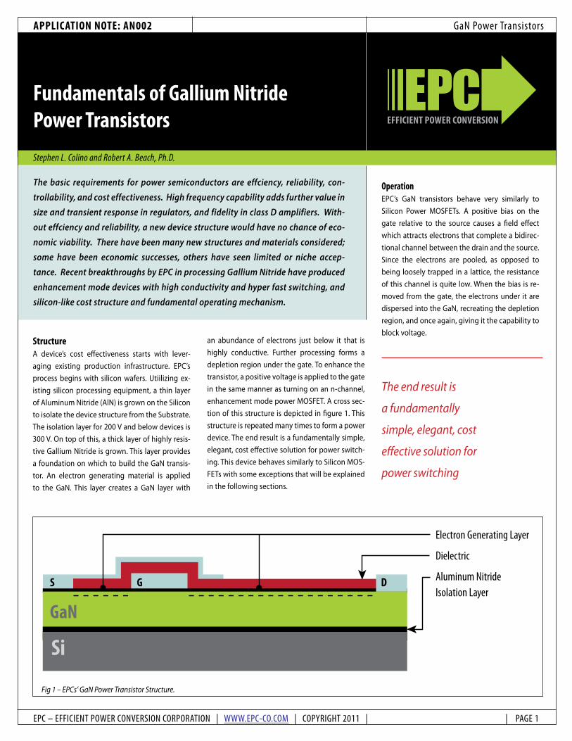
To obtain a higher voltage device, the distance between the Drain and Gate is increased. As the resistivity of our GaN pool is very low, the im-pact on resistance by increasing blocking volt-age capability is much lower when compared with Silicon. Figure 2 shows the theoretical resistance times die area limits of GaN versus Silicon versus voltage. EPC’s first generation of devices is shown as well. Please note that af-ter 30 years of Silicon MOSFET development, it has approached its theoretical limits. Progress in silicon has slowed to the point where small gains have significant development cost. GaN is young in its life cycle, and will see significant
improvement in the years to come.
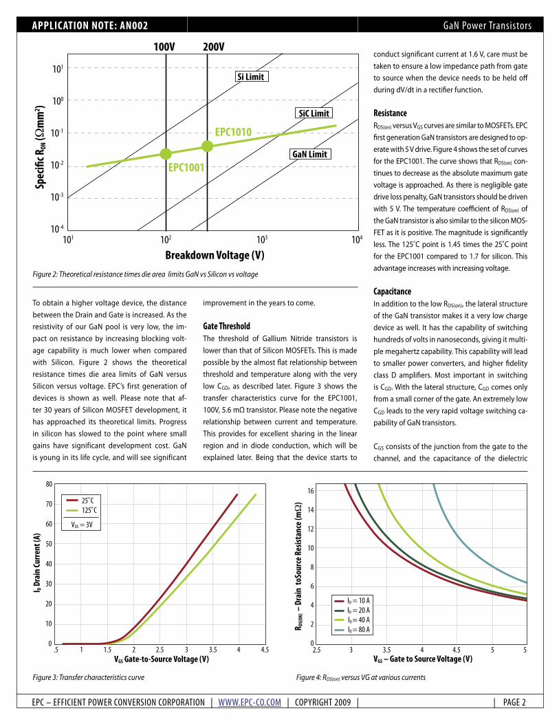
Gate ThresholdThe threshold of Gallium Nitride transistors is lower than that of Silicon MOSFETs. This is made possible by the almost flat relationship between threshold and temperature along with the very low CGD, as described later. Figure 3 shows the transfer characteristics curve for the EPC1001, 100V, 5.6 mΩ transistor. Please note the negative relationship between current and temperature. This provides for excellent sharing in the linear region and in diode conduction, which will be explained later. Being that the device starts to
conduct significant current at 1.6 V, care must be taken to ensure a low impedance path from gate to source when the device needs to be held off during dV/dt in a rectifier function.
ResistanceRDS(on) versus VGS curves are similar to MOSFETs. EPC first generation GaN transistors are designed to op-erate with 5 V drive. Figure 4 shows the set of curves for the EPC1001. The curve shows that RDS(on) con-tinues to decrease as the absolute maximum gate voltage is approached. As there is negligible gate drive loss penalty, GaN transistors should be driven with 5 V. The temperature coefficient of RDS(on) of the GaN transistor is also similar to the silicon MOS-FET as it is positive. The magnitude is significantly less. The 125˚C point is 1.45 times the 25˚C point for the EPC1001 compared to 1.7 for silicon. This advantage increases with increasing voltage.
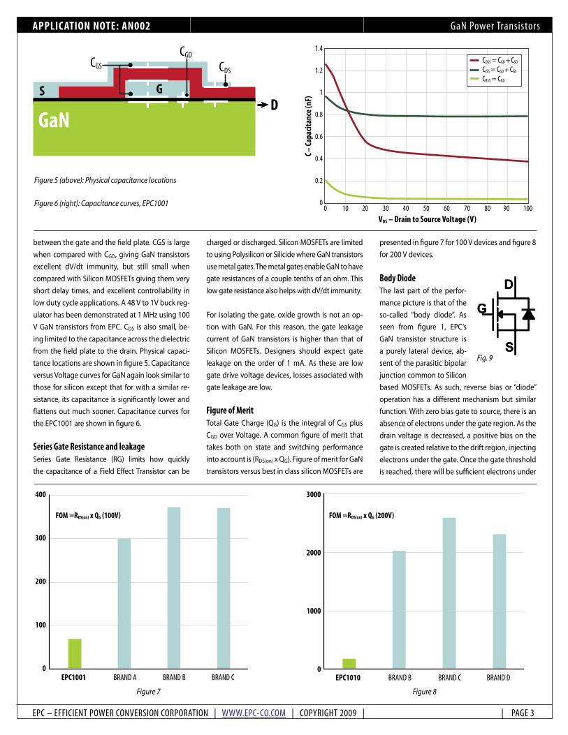
Capacitance In addition to the low RDS(on), the lateral structure of the GaN transistor makes it a very low charge device as well. It has the capability of switching hundreds of volts in nanoseconds, giving it multi-ple megahertz capability. This capability will lead to smaller power converters, and higher fidelity class D amplifiers. Most important in switching is CGD. With the lateral structure, CGD comes only from a small corner of the gate. An extremely low CGD leads to the very rapid voltage switching ca-pability of GaN transistors.
CGS consists of the junction from the gate to the channel, and the capacitance of the dielectric
GaN Limit
101
100
10-1
10-2
10-3
10-4
101 102 103 104
SiC Limit
Si Limit
100V
Breakdown Voltage (V)
R ON (Ω
mm
2 )200V
EPC1010
EPC1001
Figure 2: Theoretical resistance times die area limits GaN vs Silicon vs voltage
Figure 3: Transfer characteristics curve Figure 4: RDS(on) versus VG at various currents
I D Dr
ain
Curre
nt (A
)
VGS Gate-to-Source Voltage (V)
80
70
60
50
40
30
20
10
0.5 1 1.5 2 2.5 3 3.5 4 4.5
25˚C125˚C
VDS = 3V
R DS(
ON) –
Dra
in t
oSou
rce R
esist
ance
(mΩ
)
VGS – Gate to Source Voltage (V)
16
14
12
10
8
6
4
2
02.5 3 3.5 4 4.5 5 5.
ID = 10 AID = 20 AID = 40 AID = 80 A
APPLICATION NOTE: AN002
EPC – EFFICIENT POWER CONVERSION CORPORATION | WWW.EPC-CO.COM | COPYRIGHT 2009 | | PAGE 3
GaN Power Transistors
between the gate and the field plate. CGS is large when compared with CGD, giving GaN transistors excellent dV/dt immunity, but still small when compared with Silicon MOSFETs giving them very short delay times, and excellent controllability in low duty cycle applications. A 48 V to 1V buck reg-ulator has been demonstrated at 1 MHz using 100 V GaN transistors from EPC. CDS is also small, be-ing limited to the capacitance across the dielectric from the field plate to the drain. Physical capaci-tance locations are shown in figure 5. Capacitance versus Voltage curves for GaN again look similar to those for silicon except that for with a similar re-sistance, its capacitance is significantly lower and flattens out much sooner. Capacitance curves for the EPC1001 are shown in figure 6.
Series Gate Resistance and leakage Series Gate Resistance (RG) limits how quickly the capacitance of a Field Effect Transistor can be
charged or discharged. Silicon MOSFETs are limited to using Polysilicon or Silicide where GaN transistors use metal gates. The metal gates enable GaN to have gate resistances of a couple tenths of an ohm. This low gate resistance also helps with dV/dt immunity.
For isolating the gate, oxide growth is not an op-tion with GaN. For this reason, the gate leakage current of GaN transistors is higher than that of Silicon MOSFETs. Designers should expect gate leakage on the order of 1 mA. As these are low gate drive voltage devices, losses associated with gate leakage are low.
Figure of Merit Total Gate Charge (QG) is the integral of CGS plus CGD over Voltage. A common figure of merit that takes both on state and switching performance into account is (RDS(on) x QG). Figure of merit for GaN transistors versus best in class silicon MOSFETs are
presented in figure 7 for 100 V devices and figure 8 for 200 V devices.
Body Diode The last part of the perfor-mance picture is that of the so-called “body diode”. As seen from figure 1, EPC’s GaN transistor structure is a purely lateral device, ab-sent of the parasitic bipolar junction common to Silicon based MOSFETs. As such, reverse bias or “diode” operation has a different mechanism but similar function. With zero bias gate to source, there is an absence of electrons under the gate region. As the drain voltage is decreased, a positive bias on the gate is created relative to the drift region, injecting electrons under the gate. Once the gate threshold is reached, there will be sufficient electrons under
S GD
CGS
CGD
CDS
GaN
C – Ca
pacit
ance
(nF)
VDS – Drain to Source Voltage (V)
1.4
1.2
1
0.8
0.6
0.4
0.2
00 10 20 30 40 50 60 70 80 90 100
COSS = CGD + CSD
CISS = CGD + CGS
CRSS = CGD
Figure 5 (above): Physical capacitance locations
Figure 6 (right): Capacitance curves, EPC1001
Fig. 9
400
300
200
100
0EPC1001 BRAND A BRAND B BRAND C
FOM =RDS(on) x QG (100V)
3000
2000
1000
0EPC1010 BRAND B BRAND C BRAND D
FOM =RDS(on) x QG (200V)
Figure 7 Figure 8
APPLICATION NOTE: AN002
EPC – EFFICIENT POWER CONVERSION CORPORATION | WWW.EPC-CO.COM | COPYRIGHT 2009 | | PAGE 4
GaN Power Transistors
the gate to form a conductive channel. The benefit to this mechanism is that there are no minority carriers involved in conduction, and therefore no reverse recovery losses. While QRR is zero, output capacitance (COSS) has to be charged and discharged with ev-ery switching cycle. For devices of similar RDS(on), GaN transistors have significantly lower COSS than silicon MOSFETs. As it takes threshold voltage to turn on the GaN tran-sistor in the reverse direction, the forward voltage of the “diode” is higher than silicon transistors. As with silicon MOSFETs, care should be taken to minimize diode conduction.
As fundamental operation of GaN transistors is similar to that of silicon MOSFETs, they can be rep-resented schematically the same way as shown in figure 9.
PackagingEPC’s GaN transistors are insulated from the sub-strate. This allows monolithic fabrication of mul-tiple transistors in any configuration and efficient, common heatsinking without the need for an insulating layer between the device and the heat-sink. It also forces the current for both drain and source to be collected on one side of the die. To keep the resistance low in the metal layers that collect the current, these paths must be kept short. To accomplish this, wafer level line grid arrays are
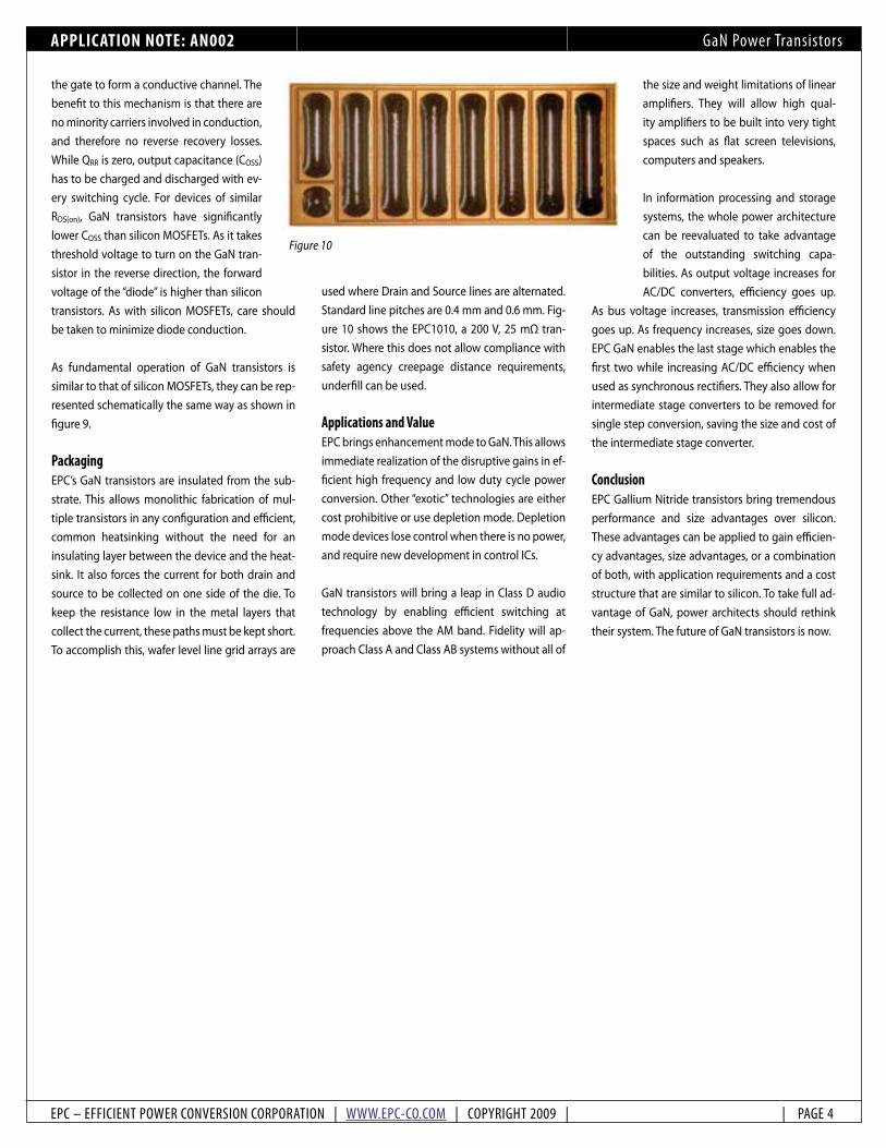
used where Drain and Source lines are alternated. Standard line pitches are 0.4 mm and 0.6 mm. Fig-ure 10 shows the EPC1010, a 200 V, 25 mΩ tran-sistor. Where this does not allow compliance with safety agency creepage distance requirements, underfill can be used.
Applications and ValueEPC brings enhancement mode to GaN. This allows immediate realization of the disruptive gains in ef-ficient high frequency and low duty cycle power conversion. Other “exotic” technologies are either cost prohibitive or use depletion mode. Depletion mode devices lose control when there is no power, and require new development in control ICs.
GaN transistors will bring a leap in Class D audio technology by enabling efficient switching at frequencies above the AM band. Fidelity will ap-proach Class A and Class AB systems without all of
the size and weight limitations of linear amplifiers. They will allow high qual-ity amplifiers to be built into very tight spaces such as flat screen televisions, computers and speakers.
In information processing and storage systems, the whole power architecture can be reevaluated to take advantage of the outstanding switching capa-bilities. As output voltage increases for AC/DC converters, efficiency goes up.
As bus voltage increases, transmission efficiency goes up. As frequency increases, size goes down. EPC GaN enables the last stage which enables the first two while increasing AC/DC efficiency when used as synchronous rectifiers. They also allow for intermediate stage converters to be removed for single step conversion, saving the size and cost of the intermediate stage converter.
ConclusionEPC Gallium Nitride transistors bring tremendous performance and size advantages over silicon. These advantages can be applied to gain efficien-cy advantages, size advantages, or a combination of both, with application requirements and a cost structure that are similar to silicon. To take full ad-vantage of GaN, power architects should rethink their system. The future of GaN transistors is now.
Figure 10