Embed Size (px)
Citation preview
8/14/2019 Future Challenges in BGA-CSP Rework - 2001
http://slidepdf.com/reader/full/future-challenges-in-bga-csp-rework-2001 1/15
8/14/2019 Future Challenges in BGA-CSP Rework - 2001
http://slidepdf.com/reader/full/future-challenges-in-bga-csp-rework-2001 2/15
automated equipment, the cost of rework is ever increasing due to the higher level of skill andexpertise required to work with the varying and delicate technologies.
As MEPs are surely finding their way into every product, repair and rework centers will have todeal with them. There are some subtle differences between reworking standard packages andMEPs. Some of the areas that will be explored are:
1. Removal of Old Package and Site Preparation2. Placement3. Flux/Paste Application4. Bottom Side Heating5. Heating Process Considerations related to package construction
Characteristics of Standard Packages and MEPs:
Standard packages can vary in size from 5.0 mm square to 50 mm square and larger. They havesolder ball diameters between .5 and 1.05 mm with pitches between .9 and 1.5 mm. Thesepackages are generally thicker than 1.5 mm. Standard packages usually contain a silicon diemounted to a substrate that is encapsulated with a plastic or resin material. Ceramic
encapsulation and substrates are also common.
MEPs can vary in size from 1.5 to 20 mm square. Solder ball diameters between .1 and .4 mmare common and pitches can range from .25 to .8 mm. MEPs are usually less than 1 mm thickand come in a variety of package configurations and some types have no package. An exampleof this type of MEP is a Flip Chip. These are essentially the silicon die that may or may not havea protective coating on the top. CSPs have a small package around them, by definition; thepackage can be no larger than 1.2 times the size of the silicon die. The encapsulating material isusually some type of polymer.
CSPs can actually fall into either category, depending on the package, ball diameter, and pitch.The number of interconnects can vary widely and is not an absolute defining characteristic.
As packages are running at higher speeds and requiring more energy, they are also being askedto operate at hotter temperatures. One way of reducing the thermal stress to the IC is to includea heat spreader in the package design. As examples, Super BGAs and the TI DSP contain metalheat spreaders.
Removal of old package and Site Preparation:
When removing packages from PCBs, the approach should be driven by the reason for theremoval and whether or not the component will be reused. When removing a package because ithas failed, a removal profile may be developed that uses faster ramp rates and shorter timesbecause we are not concerned about the survivability package. However, when a device isintended to be reused, a removal profile similar to the installation profile with slow and even
heating or the installation profile itself should be used. This is also the case when dealing withPCBs and packages that are made from materials that must adhere to ramp rate guidelines.
Regardless of the approach, proper pre-heating and thorough PCB warming is critical to thesuccess. Removing packages by only applying heat from the top should be avoided. Thistechnique can easily result in pads being damaged or lifted. The amount of heat required to bringthe solder balls to melting temperature through topical application will often overheat the reworksite and will usually exceed recommended heating ramps. It also causes significant temperaturedifferences between the top and bottom of the device and PCB, which can cause twisting, flexingand damage to micro-vias and other delicate circuitry as well as delamination of the package.
8/14/2019 Future Challenges in BGA-CSP Rework - 2001
http://slidepdf.com/reader/full/future-challenges-in-bga-csp-rework-2001 3/15
Package delamination is a common problem that is becoming more common as layers of differentmaterials are being used in the component’s construction.
It is extremely important that all the solder joints under the package are liquidus before lifting thepackage from the PCB. Rework equipment that utilize devices to automatically lift a packageafter the removal profile is completed are common and generally work well. However, if they areused, the removal profile must be validated through the use of thermocouples to ensure propertemperatures are reached. Should one or a few solder joints not reach solder melt temperaturesand the automated head lifts up, pads can and will be pulled off the PCB. Pads and traces forMEPs are often very delicate and cannot be repaired.
Another consideration when vacuum cups are used inside of the nozzle is that the vacuum cupsshield a portion of the component resulting in uneven heating. Typically, this is not a major issuein larger packages because they have longer heating cycles that allow the entire package toreach a homogenous temperature. Because MEPs have shorter heating cycles, are thinner andhave different materials compositions than their standard cousins, they are more likely to develop“cool spots” under the vacuum cup which can result in non-liquidus solder joints. To avoid paddamage, the duration or dwell time of the reflow phase can be increased. The use ofthermocouples when developing and validating profiles should become standard practice in everyrework facility.
Once a package has been removed, the rework site must be properly prepared for the nextinstallation. Excess solder on the land patterns with pads larger than .8 mm can usually beremoved using one of a variety of conductive desoldering tools available. Other techniquesinclude the use of solder wick or the use of hot gas heating. Removing excess solder from landsites with pads less that .5 mm requires a very delicate hand. If conductive desoldering tools areselected, a light touch and low temperatures must be used. Temperatures over 200 degrees Ccombined with pressure can easily damage pads or the solder mask.
In general, PCBs that have vias through them are not good candidates for purely conductivedesoldering techniques. While the desoldering tip is moved across the land pattern, the vias canbecome filled with solder. These are not easy to clean out and attempting to do so can result indamage to the via, solder mask or the PCB.
Hot gas removal systems or conductive systems incorporating hot gas assisted heating that useTeflon or stainless steel tips at low temperatures and are preferred. The use of solder wick isgenerally not recommended for MEP land preparation, unless it is used in the hands of a veryskilled technician.
“Bumping” of the lands is another technique used to remove excess solder or to add additionalsolder to the rework site by using a soldering iron tip to reflow the solder on the pads and level itas well. This technique is quite common when placing leaded devices. Typically, flux is appliedto the land site, and then a tinned tip is drawn across the array. The surface tension of the solderis relied upon to control the volume of solder left behind on the pad.
If pads are bumped, they will be rounded, not flat. Therefore, a sticky or gel flux must be used in
to hold the package in position. During Soak when the flux is activated and driven off, thepackage will usually move and can easily become misregistered to the land array. Whilebumping can work fairly well on standard packages, it is not recommended for MEPs land sitepreparation. If bumping is used on MEPs, a number of issues must be considered. The amountof solder involved with a MEPs interconnect is very small. Using old solder can result in poorquality joints and adding too much can result in bridging. Often, MEPs pads are so small indiameter, that the surface tension of the solder on the tip will just pull the solder over the pad,leaving just a thin covering behind. Additionally, drawing a hot iron tip over the MEPs array candamage and lift pads. The most significant issue is that the solder bumps will not be perfectly
8/14/2019 Future Challenges in BGA-CSP Rework - 2001
http://slidepdf.com/reader/full/future-challenges-in-bga-csp-rework-2001 4/15
level. When installing packages with ball diameters as small as .1 mm, it doesn’t take much toend up with an unlevel package, which can result in “opens”.
Once the excess solder has been removed, it is important to properly clean the PCB. The padsmust be clean and free from old solder and flux residue before proceeding with the replacementof the package. When installing MEPs, proper cleaning is just as important to the process as theinstallation profile. Shorter reflow cycles, small amounts of flux used for installation, coupled withthe small volumes of solder present in each joint does not make for a forgiving reflowconfiguration.
Placement:
Placing standard packages is relatively easy and can be accomplished with commonly availabletechniques. Placement by hand is a viable option for these packages by using a template or thesilkscreen around the land pattern as a guide. A vision overlay system (VOS) can be used toensure proper alignment and is usually preferred by most operators. Typically, a minimummagnification of 35X is required to ensure proper alignment. A placement precision of .1 to .2mm in the Z travel is usually adequate.
To place MEPs successfully a VOS must be used. A minimum magnification of 80x is requiredand quite often 100x is needed to accurately align flip chips. Placement precision in the Z travelshould be 50 microns or less. When placing flip chips, 25 microns is needed.
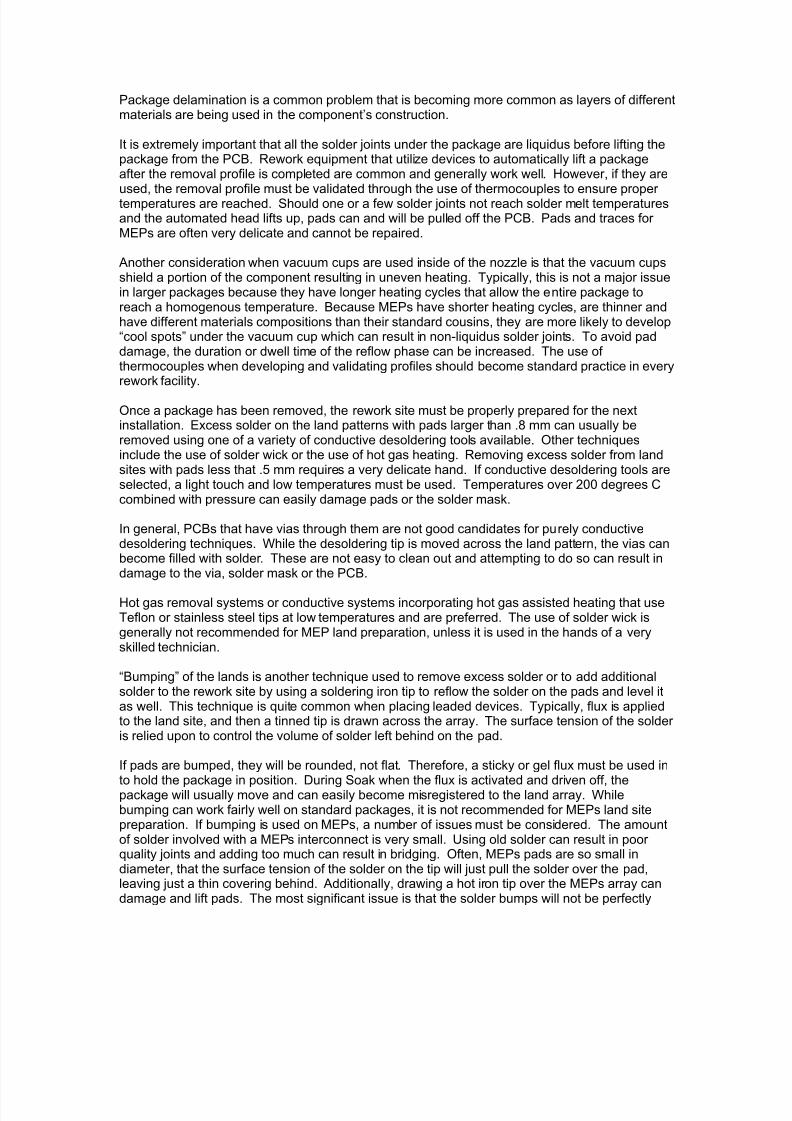
The level of precision required for placement in the Z travel mechanism is directly related to thediameter of the solder ball itself. Precision rating requirements should be calculated by using thesmallest solder ball diameter that will be reworked. To ensure proper installation, the solder ballmust cover at least 50% of the pad on the PCB. In other words, when the device is placed on thePCB the accuracy must be at least 50% in order to take advantage of the self-aligning propertiesof array packages. See Figure 1. Keep in mind that the more accuracy that can be achieved, thebetter the result. Packages that are less than 50% aligned can actually migrate one row of thearray, which results in a faulty installation.
Image courtesy of IBMFigure 1
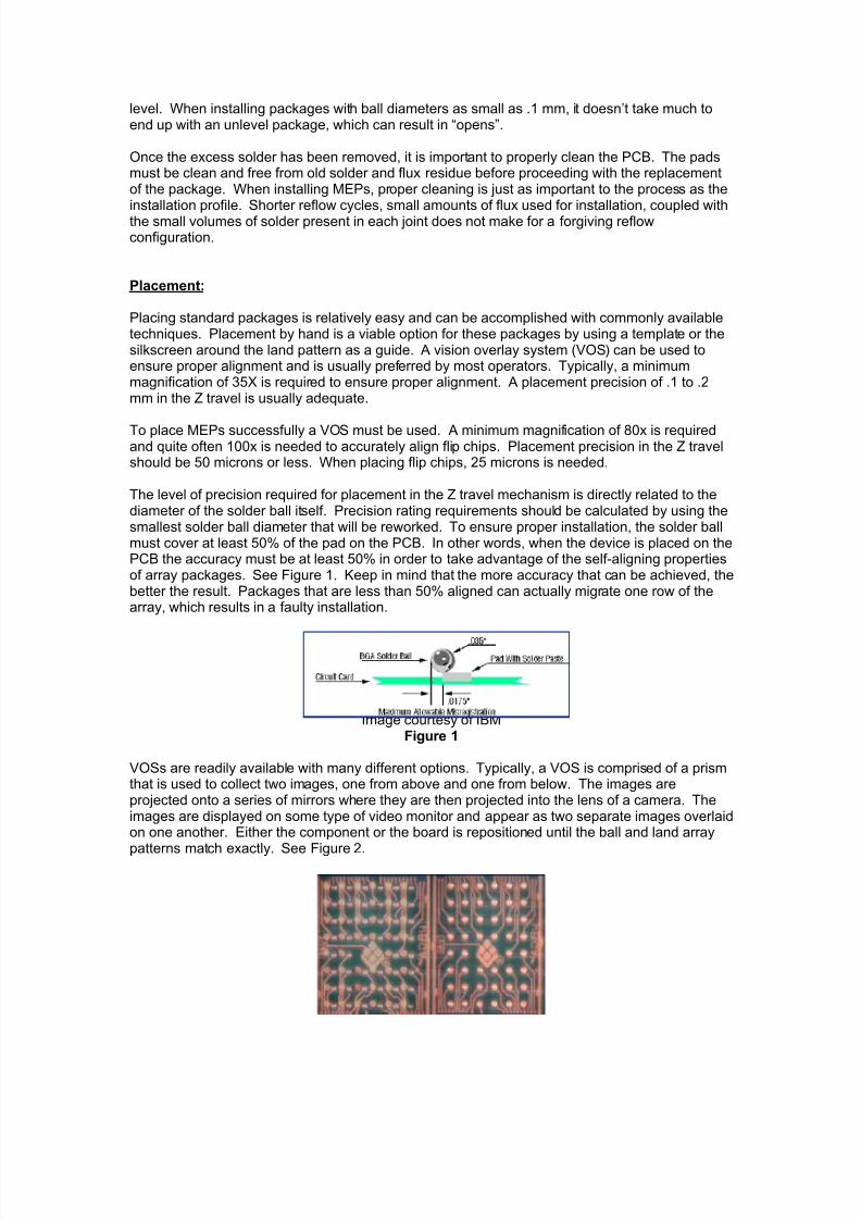
VOSs are readily available with many different options. Typically, a VOS is comprised of a prismthat is used to collect two images, one from above and one from below. The images areprojected onto a series of mirrors where they are then projected into the lens of a camera. Theimages are displayed on some type of video monitor and appear as two separate images overlaidon one another. Either the component or the board is repositioned until the ball and land array
patterns match exactly. See Figure 2.
8/14/2019 Future Challenges in BGA-CSP Rework - 2001
http://slidepdf.com/reader/full/future-challenges-in-bga-csp-rework-2001 5/15
CSP not aligned CSP alignedFigure 2.
Most VOSs used today also have a “split vision” capability, which allows the viewer to see onlytwo opposite corners of the images at a higher magnification. This is valuable when placingdevices that have hundreds of solder balls. To attempt to align more than 300 data points isdifficult. If the images can be “split” and magnified, the user can simply align two oppositecorners of the package while focusing on less than 100 points of data. See Figure 3.
Figure 3: Full view and Split Screen View
Proper care and maintenance of the VOS is important to placement success. Calibration checksshould be performed at regular intervals as indicated by the manufacturer. When adjustment isrequired, it should only be completed by qualified individuals.
Flux/Paste Application:
Flux must be used to have successful package installation. It may be used by itself or it may becombined with solder in the form of solder paste. Applying the proper amount of flux to therework site is critical. Too little flux and the solder will not flow correctly, too much flux and out-gassing can occur which result in voids within the solder joint or flux will be left over which can
cause resistivity problems as well as have corrosive effects on the solder joint after reflow. Thereare a variety of methods for applying flux. Some of the methods are to use a brush or penapplicator, to use a piston driven mechanism to dispense a gel or sticky flux, and to use a fluxapplicator tool.
When applying flux to area array packages, the ideal amount of flux to apply is enough to cover1/3 of the solder ball. This ensures that enough flux is present to clean and remove oxides whileeliminating the potential for out-gassing and excessive flux being left behind. With theintroduction of gel flux, applying precise amounts of flux to balls can be accomplished andrepeated consistently.
Solder paste should always be used when:
•
Solder balls on the bottom of the package are made from 90/10 solder.• PCBs have bare copper pads on them,
• The package contains an elastomer layer for CTE differences,
• It is critical to have the same joint geometry as the production assembly and solder pastewas used in initial production,
• No clean flux can not be used,
• A specification exists for the joint stand-off height for function or cleaning.
Solder paste can be applied using a variety of techniques. Some of the more commontechniques include using spot stencils to apply solder paste to the PCB, using component stencils

8/14/2019 Future Challenges in BGA-CSP Rework - 2001
http://slidepdf.com/reader/full/future-challenges-in-bga-csp-rework-2001 6/15
to apply solder paste to the component, and using dispensing equipment to apply dots of solderpaste to each individual pad.
Solder paste with ball sizes of #4 should be used for small pad printing. When applying solderpaste to standard packages, typically, a paste thickness of .17 to .23 mm is desired. When usingsolder paste for MEPs, a paste thickness of .1mm to .16mm is desired.
Stencil aperture shape is also an important consideration. Typically, stencils with apertures largerthan .2 mm are round and lend themselves to good release. Apertures in stencils designed forpaste deposits smaller than .2 mm are often diamond shaped. The diamond shape allows thesolder paste to release from the stencil easier than a circular one.
The Impact of Bottom-Side Heating:
Bottom side heating is usually associated with the “pre-heat” phase of a profile. However, bottomside heating is as important in Soak and Reflow phases if the installation is to be successful whileexposing the PCB and package to a minimal amount of thermal stress.
In the “Pre-heat” phase, bottom side heating ensures homogenous temperatures across the
board. This keeps the PCB from warping, twisting, or flexing, during the process, which isessential for maintaining planarity of the installation site. Heat application from the bottom of thePCB during the “pre-heat” phase is also used to warm the entire PCB so that heat is not drawnaway from the installation site during the rest of the process.
During “Soak”, the bottom side heater should continue to operate while a relatively small amountof heat is added from the top heater. The combination of top and bottom side heat applicationallows the installation site and package to reach a temperature of between 140 and 160 degreesC and to stabilize. The stabilization should be maintained for 40 to 60 seconds, allowing the fluxto activate and driving off any volatiles in the flux. This is important as it eliminates the potentialfor out-gassing and prepares the package and PCB for reflow.
During “Reflow”, heat is usually actively applied from the top heater. Top heaters generally
operate between temperatures of 200 and 350 degrees C. Obviously, this can place a lot ofthermal stress on the top of the package. It is important to apply heat slowly and evenly so theentire package warms to reflow temperature uniformly. Temperature differences across apackage of as little as 5 to 10 degrees C can cause damage.
The set temperature of the bottom heater can be maintained or increased during reflow.Increasing the temperature by as little as 15 degrees C during reflow will have a dramatic impacton the package profile. One of the many benefits of adding additional heat from the bottom or“Spiking” during the reflow phase is that lower temperatures can be applied from the top.
Installations should always be achieved with the lowest temperatures possible. This ensures thesafety of the package as well as PCB. Additionally, by subjecting the package to lowertemperatures, there is less chance for temperature overshooting which can result in significant
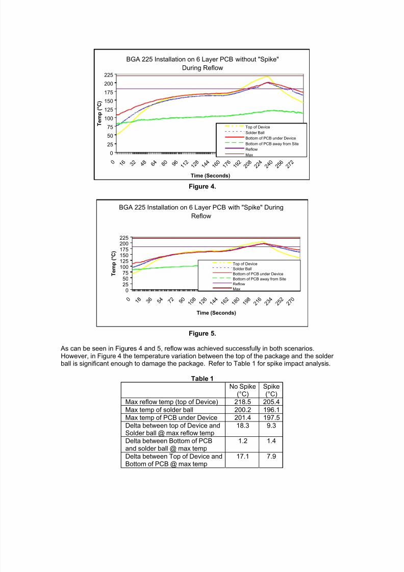
temperature variations between the top of the package, bottom of the package, the solder jointand PCB. See Figures 4 and 5.
8/14/2019 Future Challenges in BGA-CSP Rework - 2001
http://slidepdf.com/reader/full/future-challenges-in-bga-csp-rework-2001 7/15
BGA 225 Installation on 6 Layer PCB without "Spike"
During Reflow
0
25
50
75
100
125
150
175
200
225
0 1 6 3 2 4 8 6 4 8 0 9 6 1 1 2
1 2 8
1 4 4
1 6 0
1 7 6
1 9 2
2 0 8
2 2 4
2 4 0
2 5 6
2 7 2
Time (Seconds)
T e m p ( ° C )
Top of Device
Solder Ball
Bottom of PCB under Device
Bottom of PCB away from Site
Reflow
Max
Figure 4.
BGA 225 Installation on 6 Layer PCB with "Spike" During
Reflow
0255075
100125150175200225
0 1 8 3 6 5 4 7 2 9 0 1 0 8 1 2 6 1 4 4 1 6 2 1 8 0 1 9 8 2 1 6 2 3 4 2 5 2 2 7 0
Time (Seconds)
T e m p ( ° C )
Top of Device
Solder Ball
Bottom of PCB under Device
Bottom of PCB away from Site
Reflow
Max
Figure 5.
As can be seen in Figures 4 and 5, reflow was achieved successfully in both scenarios.However, in Figure 4 the temperature variation between the top of the package and the solderball is significant enough to damage the package. Refer to Table 1 for spike impact analysis.
Table 1
No Spike(°C)
Spike(°C)
Max reflow temp (top of Device) 218.5 205.4Max temp of solder ball 200.2 196.1
Max temp of PCB under Device 201.4 197.5
Delta between top of Device andSolder ball @ max reflow temp
18.3 9.3
Delta between Bottom of PCBand solder ball @ max temp
1.2 1.4
Delta between Top of Device andBottom of PCB @ max temp
17.1 7.9
8/14/2019 Future Challenges in BGA-CSP Rework - 2001
http://slidepdf.com/reader/full/future-challenges-in-bga-csp-rework-2001 8/15
By controlling the application of heat from the top and bottom of the installation site, more evenheating can be achieved. This can be seen in lower temperature variances between the top andbottom of the package and between solder balls located on the outer edge and in the middle ofthe array pattern.
Heating Process Considerations:
While standard BGAs and MEPs look similar in design, they are actually quite different anddemand different profile configurations when it comes to installation and removal profiles.Physically, they differ in several areas: materials, dimension, mass, and tolerances totemperature. In general, profiles used to install MEPs are shorter than profiles for standardpackages. Also, lower temperatures can and should be used when installing MEPs. Becausethe MEPs package is the size of the silicon die, or slightly larger, there is no significantencapsulation for protection, heat is applied/transferred directly to the silicon.
The smaller mass of the MEP solder balls, coupled with a very thin package allows heat to betransferred through the component very quickly. When standard BGAs are installed, heat mustbe driven through and around the package, which requires a longer heat application period.
Therefore, if a profile for a standard package is used on a MEP, the component will becomesuper heated which is something that must be avoided.
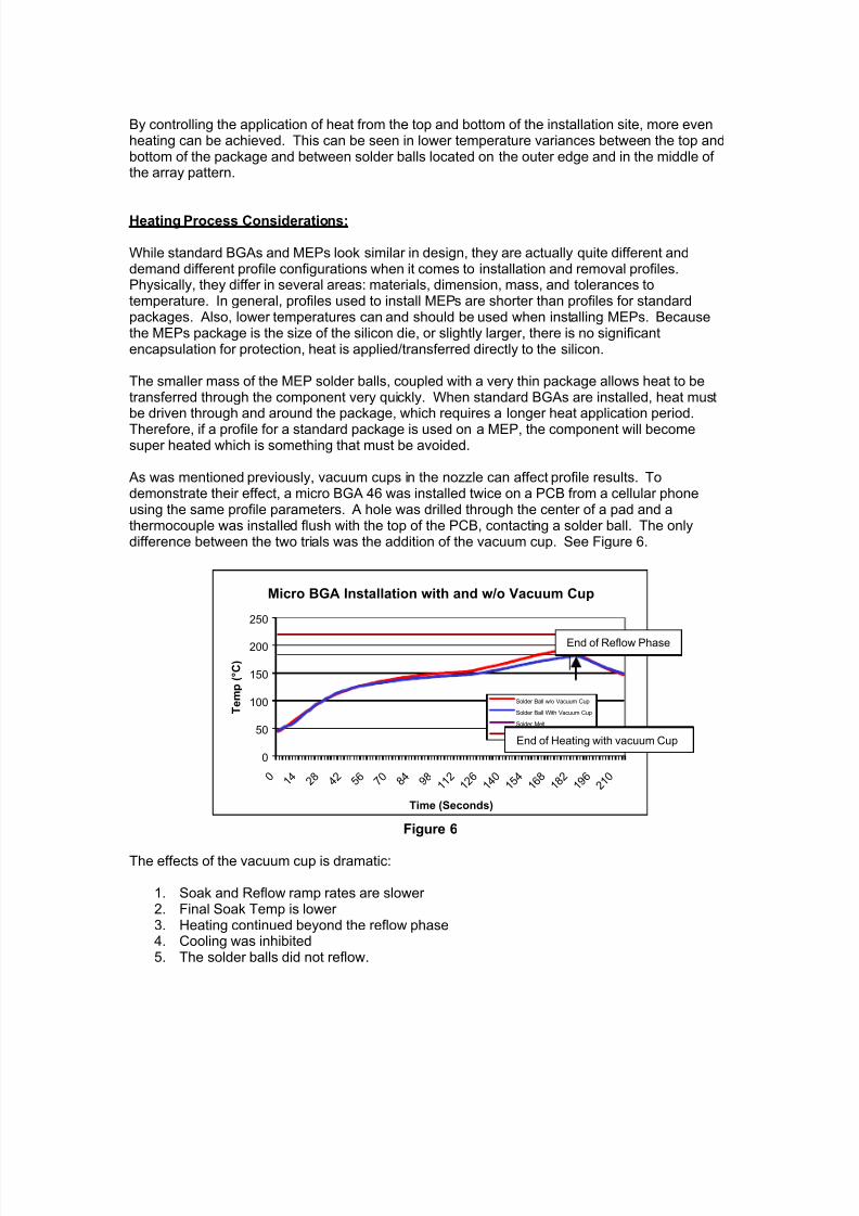
As was mentioned previously, vacuum cups in the nozzle can affect profile results. Todemonstrate their effect, a micro BGA 46 was installed twice on a PCB from a cellular phoneusing the same profile parameters. A hole was drilled through the center of a pad and athermocouple was installed flush with the top of the PCB, contacting a solder ball. The onlydifference between the two trials was the addition of the vacuum cup. See Figure 6.
Micro BGA Installation with and w/o Vacuum Cup
0
50
100
150
200
250
0 1 4 2 8 4 2 5 6 7 0 8 4 9 8 1 1 2
1 2 6
1 4 0
1 5 4
1 6 8
1 8 2
1 9 6
2 1 0
Time (Seconds)
T e m p ( ° C )
Solder Ball w/o Vacuum Cup
Solder Ball With Vacuum Cup
Solder Melt
Max Temp
Figure 6
The effects of the vacuum cup is dramatic:
1. Soak and Reflow ramp rates are slower2. Final Soak Temp is lower3. Heating continued beyond the reflow phase4. Cooling was inhibited5. The solder balls did not reflow.
End of Reflow Phase
End of Heating with vacuum Cup
8/14/2019 Future Challenges in BGA-CSP Rework - 2001
http://slidepdf.com/reader/full/future-challenges-in-bga-csp-rework-2001 9/15
In this case, the vacuum cup used was round so the edges and corners of the micro BGA wereexposed to more heat than the portion of the package under the vacuum cup. This results inhigher temperature variations across the entire package.
There are many methods for applying heat as well as different methods to monitor and control it. Arguments can be made for all. Heaters used in area array rework equipment are almost alwayscontrolled through closed loop structures. This means that the heater is cycled on and off basedon the condition of the thermal sensor. In many cases the variation between set temperaturesand actual temperatures between area array rework equipment is due to the position of thesensors.
Sensor placement can dramatically affect the result of set temperatures, which is why a validprofile configuration developed on one rework machine does not usually successfully transfer toanother. Ultimately the set values on a particular machine are not critical. What is critical,however, is the thermal environment those set temperatures create around the package andPCB. Profiles should always be created and validated using feedback from thermocouples.
Many systems allow profile settings to be adjusted while a profile cycle is running. Usually a PCBwill be populated with thermocouples in a number of locations. It is good practice to placethermocouples:
• on the top of the device,
• on at least one solder ball, 2 is better (inner and outer ball), and
• on the bottom-side of the PCB, both, directly under the rework site and away from therework site.
Positioning thermocouples in these locations allows:
• monitoring of temperature variations between the top and bottom of the package,
• monitoring of temperature variations between the middle and outer edge of the package,as well as
• monitoring of the thermal environment the solder balls are exposed to.
Monitoring the temperature directly below the rework site is important as PCBs can be subjectedto too much heat, as can packages. This can cause damage to circuitry, micro vias, anddelamination of the PCB itself. The purpose of the thermocouple on the bottom of the PCB awayfrom the rework site is to ensure the entire board is warmed properly and is not exposed to hightemperatures in one location, under the rework site.
Profiling can be accomplished using a site containing a previously installed package, or byperforming an actual installation. Either method can be used to develop a reliable profile.However, there are some issues to be aware of with each.
If using a site where a package is already installed, the placement of the thermocouples isimportant. They must have contact with the existing solder joints. This is best accomplished bydrilling through the bottom of the board into a solder joint and affixing the thermocouple with an
adhesive or other means to secure it. Affixing a thermocouple to the top of the package that isalready soldered is easier in most cases, especially when MEPs are involved.
When developing profiles through an actual installation, it is important to make sure the solderballs are touching the thermocouples through out the entire process. Should a thermocouple losecontact with the solder balls, bad data will be collected. Additionally, it is often difficult to affix athermocouple to the top of a loose package and successfully maintain contact with the PCBduring the process.
8/14/2019 Future Challenges in BGA-CSP Rework - 2001
http://slidepdf.com/reader/full/future-challenges-in-bga-csp-rework-2001 10/15
Feedback from the thermocouples will assist the operator in adjusting the time and temperatureparameters. In general, the following guidelines should be adhered to when developing profiles.
Ramp and Maximum Temperatures
Acceptable ramp rates and maximum temperatures can be obtained from the packagemanufacturer. It is wise to select a maximum temperature that allows a margin of safetyto the manufacturer’s specification.
Pre-Heat
1. If a “step profile” is desired, the top of the PCB should reach a stable temperature of95 to 105 ºC during pre-heat. Stability is the main goal here. When plotting a curve, thetrace should level off at this temperature.
2. If a linear slope is desired, preheat is merged with the soak phase. In this method, thepackage and PCB are warmed at a constant rate (the ramp rate usually 1 to 3 ºC/s) untilthe desired soak temperature is reached.
Soak
Soak is a critical step in the process. It is used to activate the flux and to drive offvolatiles and excess flux. It is important that a soak temperature between 145 and 165ºC be reached. Ideally, a relatively stable temperature should be maintained for 40 to 60seconds. This should be extended if liquid flux is brushed on to the PCB or wheninstalling a large package. Soak also allows the entire package and PCB to come to auniform temperature. If the entire package and PCB are the same temperature the rateof temperature increase in response to the additional application of heat during reflow willbe the same throughout. This allows for uniform ramping across the entire package.
Reflow
Reflow is the second to last phase in the cycle. During this phase the solder balls reach
solder melt and form the joint between the package and the pads. It is critical that allareas of the array reach solder melt together and that all balls are liquidus for at least 20to 45 seconds. Generally, Reflow for MEPs will be a shorter phase than for standardpackages. Additionally, lower temperatures can be used for MEPs as they are thinnerand have less mass. When developing profiles for MEPs it is very important to not applytoo much heat.
The type of solder used in the solder balls is variable that can greatly impact the profile ofa component. It is likely that lead free solders will be common over the next 1 to 3 years.The reflow range for is defined by: 1) the maximum temperature a component can beexposed to (usually the max minus 10 degrees C) and 2) the melting temperature ofsolder. Typically, the range for reflow , when using 63/37 solder is between 195 and 225degrees C. This is a fairly wide and forgiving range. When lead free solders are used,
the reflow range is between 210 and 225 degrees C. This is a much tighter window soslow, even uniform heating is required so the window is overshot. Again, the use ofthermocouples to validate profiles results is critical.
Another variable that must be taken into account when profiling is whether or not thecomponent has a heat spreader or not. When heat spreaders are present, therequirement for slow and even heating is more stringent. The greater the variety ofmaterials present in a given component, the greater the likelihood of delamination.
8/14/2019 Future Challenges in BGA-CSP Rework - 2001
http://slidepdf.com/reader/full/future-challenges-in-bga-csp-rework-2001 11/15
High Density Material
Cool Down
Cool down is the last phase of the cycle. It is used to bring the temperature of thepackage, solder joints, and PCB under the package below solder melt temperatures.Cooling should be controlled and a good rule of thumb is to use the same rate for cooldown as for ramp up. If the ramp rate were 2 ºC/s increase, the cool down rate would bea temperature decrease of 2 ºC/s.
Once a profile has been initially defined, it is important to re-run the profile with the determinedparameters in a static (non-changing) environment to ensure the results are valid.
Inspection
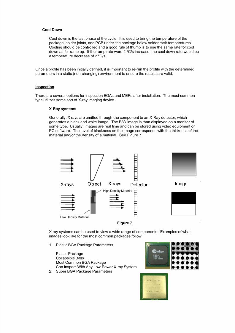
There are several options for inspection BGAs and MEPs after installation. The most commontype utilizes some sort of X-ray imaging device.
X-Ray systems
Generally, X rays are emitted through the component to an X-Ray detector, whichgenerates a black and white image. The B/W image is than displayed on a monitor ofsome type. Usually, images are real time and can be stored using video equipment orPC software. The level of blackness on the image corresponds with the thickness of thematerial and/or the density of a material. See Figure 7.
Figure 7
X ray systems can be used to view a wide range of components. Examples of whatimages look like for the most common packages follow:
1. Plastic BGA Package Parameters
Plastic PackageCollapsible BallsMost Common BGA PackageCan Inspect With Any Low-Power X-ray System
2. Super BGA Package Parameters
Ob ect Detector Image
Low Density Material
X-rays X-rays
8/14/2019 Future Challenges in BGA-CSP Rework - 2001
http://slidepdf.com/reader/full/future-challenges-in-bga-csp-rework-2001 12/15
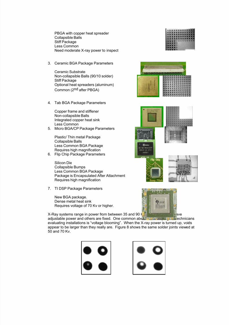
PBGA with copper heat spreaderCollapsible BallsStiff PackageLess CommonNeed moderate X-ray power to inspect
3. Ceramic BGA Package Parameters
Ceramic SubstrateNon-collapsible Balls (90/10 solder)Stiff PackageOptional heat spreaders (aluminum)
Common (2nd after PBGA)
4. Tab BGA Package Parameters
Copper frame and stiffenerNon-collapsible BallsIntegrated copper heat sinkLess Common
5. Micro BGA/CP Package Parameters
Plastic/ Thin metal PackageCollapsible BallsLess Common BGA PackageRequires high magnification
6. Flip Chip Package Parameters
Silicon DieCollapsible Bumps
Less Common BGA PackagePackage is Encapsulated After AttachmentRequires high magnification
7. TI DSP Package Parameters
New BGA package.Dense metal heat sinkRequires voltage of 70 Kv or higher.
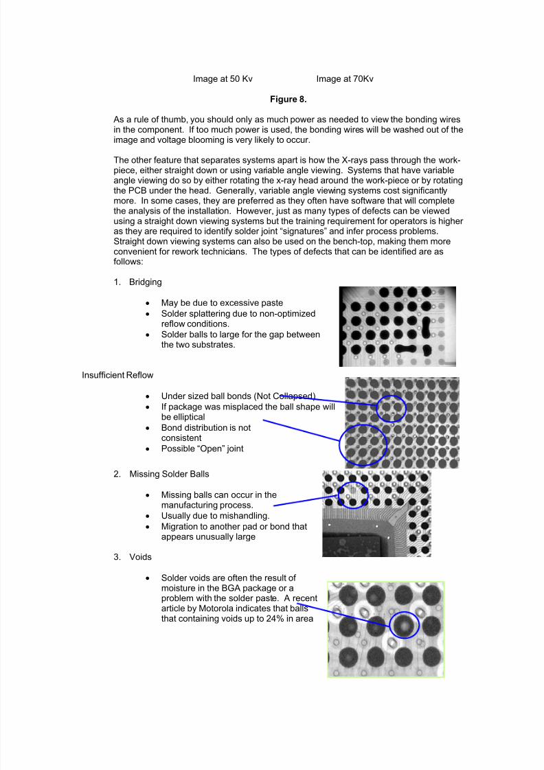
X-Ray systems range in power from between 35 and 90 Kv. Some systems haveadjustable power and others are fixed. One common aberration that plagues techniciansevaluating installations is “voltage blooming”. When the X-ray power is turned up, voids
appear to be larger than they really are. Figure 8 shows the same solder joints viewed at50 and 70 Kv.
8/14/2019 Future Challenges in BGA-CSP Rework - 2001
http://slidepdf.com/reader/full/future-challenges-in-bga-csp-rework-2001 13/15
Image at 50 Kv Image at 70Kv
Figure 8.
As a rule of thumb, you should only as much power as needed to view the bonding wiresin the component. If too much power is used, the bonding wires will be washed out of theimage and voltage blooming is very likely to occur.
The other feature that separates systems apart is how the X-rays pass through the work-piece, either straight down or using variable angle viewing. Systems that have variableangle viewing do so by either rotating the x-ray head around the work-piece or by rotatingthe PCB under the head. Generally, variable angle viewing systems cost significantlymore. In some cases, they are preferred as they often have software that will completethe analysis of the installation. However, just as many types of defects can be viewedusing a straight down viewing systems but the training requirement for operators is higheras they are required to identify solder joint “signatures” and infer process problems.Straight down viewing systems can also be used on the bench-top, making them moreconvenient for rework technicians. The types of defects that can be identified are asfollows:
1. Bridging
• May be due to excessive paste
• Solder splattering due to non-optimizedreflow conditions.
• Solder balls to large for the gap betweenthe two substrates.
Insufficient Reflow
• Under sized ball bonds (Not Collapsed)
• If package was misplaced the ball shape willbe elliptical
• Bond distribution is notconsistent
• Possible “Open” joint
2. Missing Solder Balls
• Missing balls can occur in themanufacturing process.
• Usually due to mishandling.
• Migration to another pad or bond that
appears unusually large
3. Voids
• Solder voids are often the result ofmoisture in the BGA package or aproblem with the solder paste. A recentarticle by Motorola indicates that ballsthat containing voids up to 24% in area
8/14/2019 Future Challenges in BGA-CSP Rework - 2001
http://slidepdf.com/reader/full/future-challenges-in-bga-csp-rework-2001 14/15
were more reliable than those package without voids.
• Voids are a process indicator and are not necessarily a defect unlessexcessively large.
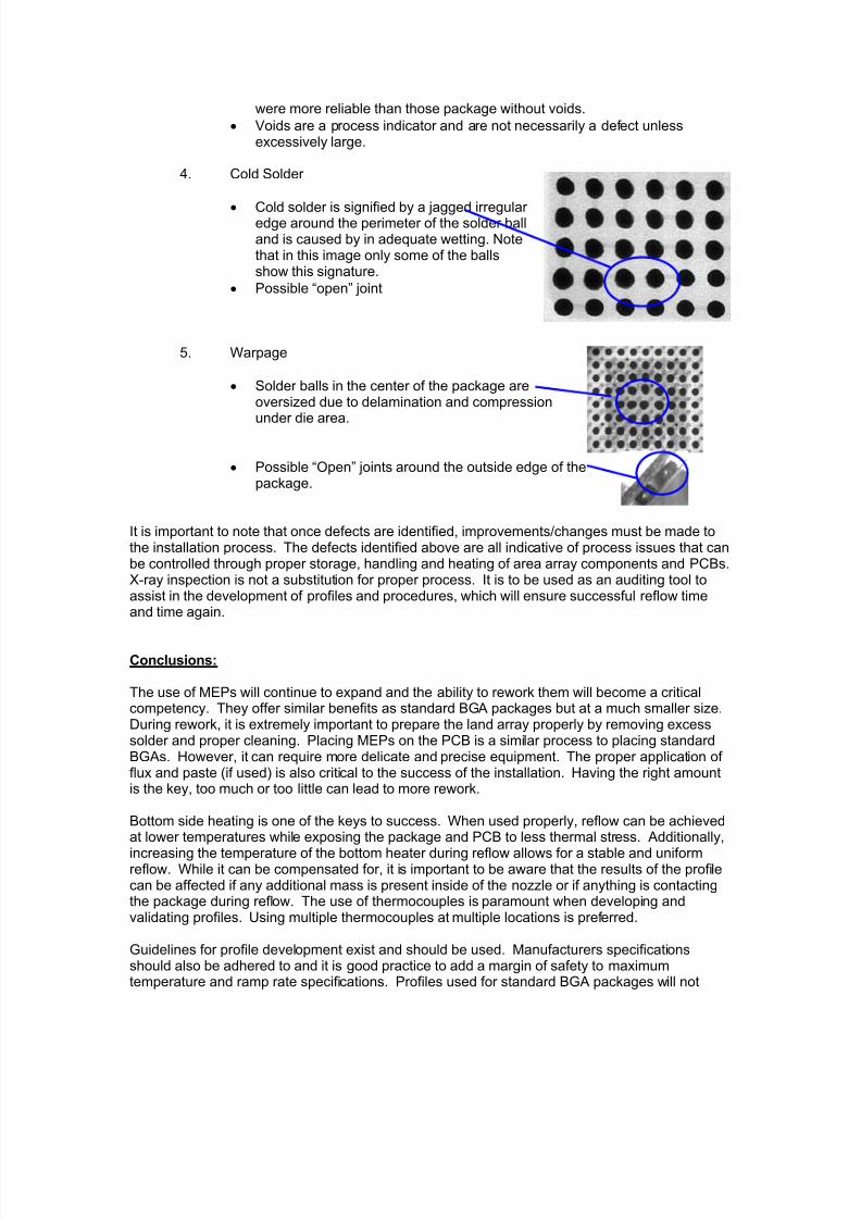
4. Cold Solder
•
Cold solder is signified by a jagged irregularedge around the perimeter of the solder balland is caused by in adequate wetting. Notethat in this image only some of the ballsshow this signature.
• Possible “open” joint
5. Warpage
• Solder balls in the center of the package areoversized due to delamination and compressionunder die area.
• Possible “Open” joints around the outside edge of thepackage.
It is important to note that once defects are identified, improvements/changes must be made tothe installation process. The defects identified above are all indicative of process issues that canbe controlled through proper storage, handling and heating of area array components and PCBs.X-ray inspection is not a substitution for proper process. It is to be used as an auditing tool toassist in the development of profiles and procedures, which will ensure successful reflow timeand time again.
Conclusions:
The use of MEPs will continue to expand and the ability to rework them will become a criticalcompetency. They offer similar benefits as standard BGA packages but at a much smaller size.During rework, it is extremely important to prepare the land array properly by removing excesssolder and proper cleaning. Placing MEPs on the PCB is a similar process to placing standardBGAs. However, it can require more delicate and precise equipment. The proper application offlux and paste (if used) is also critical to the success of the installation. Having the right amountis the key, too much or too little can lead to more rework.
Bottom side heating is one of the keys to success. When used properly, reflow can be achievedat lower temperatures while exposing the package and PCB to less thermal stress. Additionally,
increasing the temperature of the bottom heater during reflow allows for a stable and uniformreflow. While it can be compensated for, it is important to be aware that the results of the profilecan be affected if any additional mass is present inside of the nozzle or if anything is contactingthe package during reflow. The use of thermocouples is paramount when developing andvalidating profiles. Using multiple thermocouples at multiple locations is preferred.
Guidelines for profile development exist and should be used. Manufacturers specificationsshould also be adhered to and it is good practice to add a margin of safety to maximumtemperature and ramp rate specifications. Profiles used for standard BGA packages will not
8/14/2019 Future Challenges in BGA-CSP Rework - 2001
http://slidepdf.com/reader/full/future-challenges-in-bga-csp-rework-2001 15/15
transfer directly to MEPS. However, they can be used as starting points in developing the perfectprofile.
Inspection systems are a tool and should be used in the development process and to verify reflowconditions every so often. When defects are found, procedures, profiles, and proper equipmentoperation should be audited. Understanding how to read an X-ray image from a straight downviewing system allows the operator to identify the most common defects without having to spendsignificant dollars on equipment.
References:
1. Kevin Towle, Line Configuration for Today’s Highly Complex Manufacturing, SMT Magazine,11/98
2. Japan Printed Circuit Association, Report on the Technology Road Map for AdvancedSystem Integration and Packaging, 1998
3. Mike Bixenman and Treliant Fang, Wafer Solder Bumping, Advanced Packaging, 6/994. Mike Sauer and Kristina Bergman, Rework & Repair, SMT Magazine, 7/995. Paul Wood, New Considerations in CSP Rework, Circuits Assembly, 7/996. Mei Wang, Kazu Nakajima, et al, Investigation of the Printing Process for CSP Assembly,
SMTA 1999 Conference Proceedings.