Embed Size (px)
Citation preview
© Dr. Lynn Fuller, Motorola Professor
Rochester Institute of TechnologyMicroelectronic Engineering
GaAs Device Technology
Page 1
ROCHESTER INSTITUTE OF TECHNOLOGYMICROELECTRONIC ENGINEERING
Gallium Arsenide Devices, Technologies& Integrated Circuits
Dr. Lynn Fuller Motorola Professor
Microelectronic Engineering Rochester Institute of Technology 82 Lomb Memorial Drive Rochester, NY 14623-5604 Tel (585) 475-2035 Fax (585) 475-5041 [email protected]
11-4-2001 gaas.ppt
© Dr. Lynn Fuller, Motorola Professor
Rochester Institute of TechnologyMicroelectronic Engineering
GaAs Device Technology
Page 2
OUTLINE
Comparison of Silicon and GaAsMBEGaAs MESFETMESFET Test ResultsIC Process TechnologyReferences
© Dr. Lynn Fuller, Motorola Professor
Rochester Institute of TechnologyMicroelectronic Engineering
GaAs Device Technology
Page 3
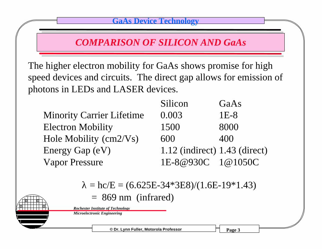
COMPARISON OF SILICON AND GaAs
Silicon GaAsMinority Carrier Lifetime 0.003 1E-8Electron Mobility 1500 8000Hole Mobility (cm2/Vs) 600 400Energy Gap (eV) 1.12 (indirect) 1.43 (direct)Vapor Pressure 1E-8@930C 1@1050C
The higher electron mobility for GaAs shows promise for highspeed devices and circuits. The direct gap allows for emission ofphotons in LEDs and LASER devices.
λ = hc/E = (6.625E-34*3E8)/(1.6E-19*1.43) = 869 nm (infrared)
© Dr. Lynn Fuller, Motorola Professor
Rochester Institute of TechnologyMicroelectronic Engineering
GaAs Device Technology
Page 4
CRYSTAL GROWTH and OXIDES OF GaAs
The vapor pressure of As in GaAs is quite low. A GaAs substrateheated to about 500 C begins to lose As from the surface. The wafercan be capped with SiO2 or Si3N4 or the heat treating can be carriedout in an Arsenic over pressure. GaAs crystals are often grown in thehorizontal Bridgeman technique and the wafers are “D” shaped.Czochralski GaAs wafers are also available up to ~4” in diameter.GaAs wafers are more brittle than Silicon wafers. 4” GaAs waferscost about $300 each.
GaAs does not grow a native oxide that is equivalent to SiO2.Ga2O3 and As2O3 and As2O5 oxides that grow on GaAs presentmore problems than uses.
© Dr. Lynn Fuller, Motorola Professor
Rochester Institute of TechnologyMicroelectronic Engineering
GaAs Device Technology
Page 5
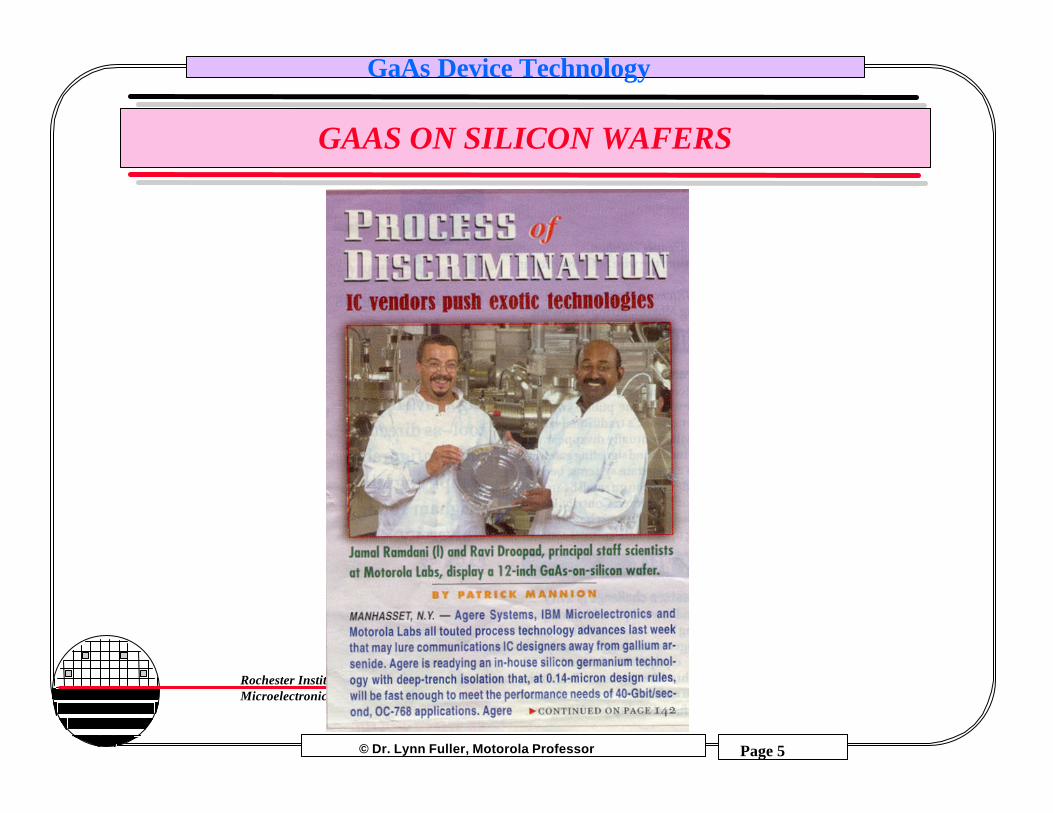
GAAS ON SILICON WAFERS
© Dr. Lynn Fuller, Motorola Professor
Rochester Institute of TechnologyMicroelectronic Engineering
GaAs Device Technology
Page 6
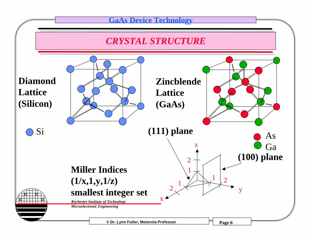
CRYSTAL STRUCTURE
xy
z
21
11
2
2
DiamondLattice(Silicon)
Miller Indices(1/x,1,y,1/z)smallest integer set
(100) plane
(111) plane
ZincblendeLattice(GaAs)
AsGa
Si
© Dr. Lynn Fuller, Motorola Professor
Rochester Institute of TechnologyMicroelectronic Engineering
GaAs Device Technology
Page 7
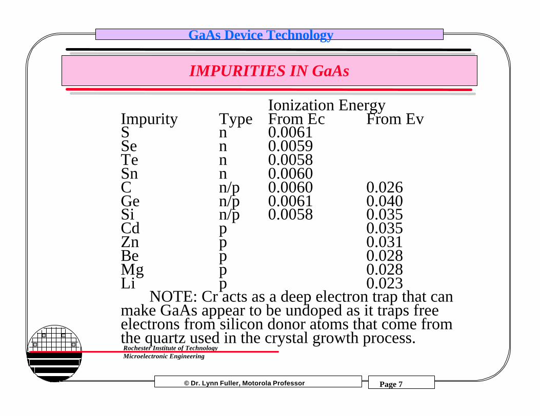
IMPURITIES IN GaAs
Ionization EnergyImpurity Type From Ec From EvS n 0.0061Se n 0.0059Te n 0.0058Sn n 0.0060C n/p 0.0060 0.026Ge n/p 0.0061 0.040Si n/p 0.0058 0.035Cd p 0.035Zn p 0.031Be p 0.028Mg p 0.028Li p 0.023 NOTE: Cr acts as a deep electron trap that canmake GaAs appear to be undoped as it traps freeelectrons from silicon donor atoms that come fromthe quartz used in the crystal growth process.
© Dr. Lynn Fuller, Motorola Professor
Rochester Institute of TechnologyMicroelectronic Engineering
GaAs Device Technology
Page 8
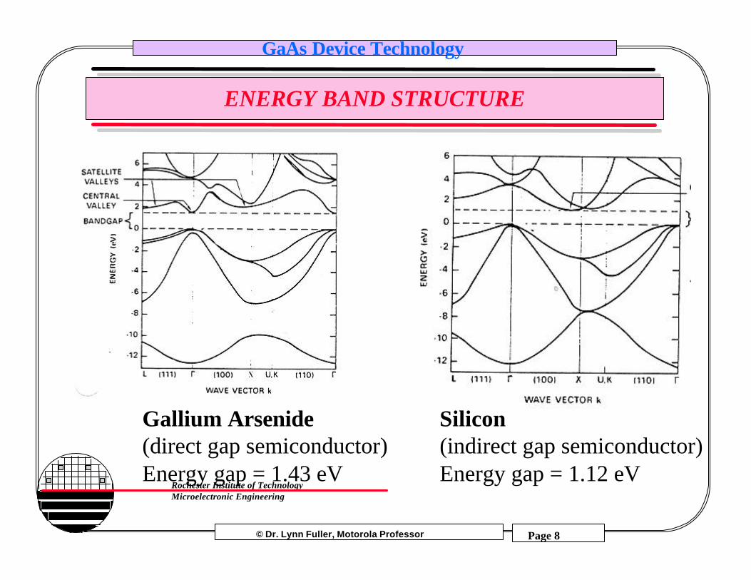
ENERGY BAND STRUCTURE
Gallium Arsenide(direct gap semiconductor)Energy gap = 1.43 eV
Silicon(indirect gap semiconductor)Energy gap = 1.12 eV
© Dr. Lynn Fuller, Motorola Professor
Rochester Institute of TechnologyMicroelectronic Engineering
GaAs Device Technology
Page 9
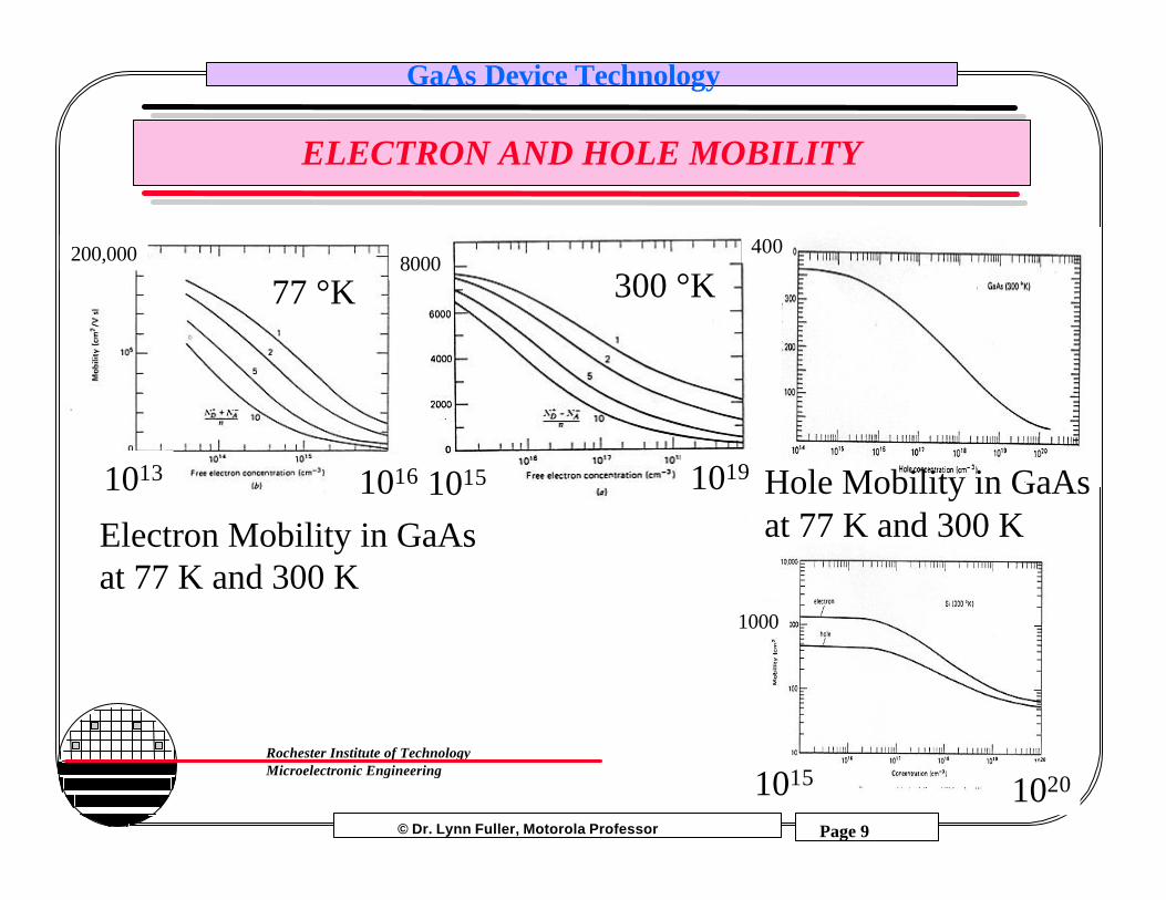
ELECTRON AND HOLE MOBILITY
300 °K77 °K8000
1015 101910161013
200,000
Electron Mobility in GaAsat 77 K and 300 K
Hole Mobility in GaAsat 77 K and 300 K
1000
400
1015 1020
© Dr. Lynn Fuller, Motorola Professor
Rochester Institute of TechnologyMicroelectronic Engineering
GaAs Device Technology
Page 10
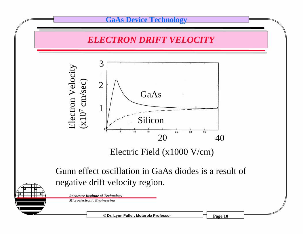
ELECTRON DRIFT VELOCITY
GaAs
Silicon
Electric Field (x1000 V/cm)
Ele
ctro
n V
eloc
ity(x
107 c
m/s
ec)
3
2
1
20 40
Gunn effect oscillation in GaAs diodes is a result ofnegative drift velocity region.
© Dr. Lynn Fuller, Motorola Professor
Rochester Institute of TechnologyMicroelectronic Engineering
GaAs Device Technology
Page 11
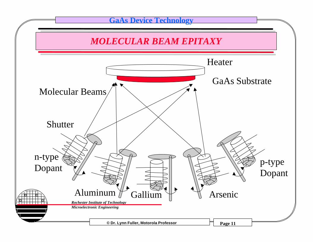
MOLECULAR BEAM EPITAXY
GalliumAluminum
Shutter
n-typeDopant
Arsenic
p-typeDopant
GaAs Substrate
Heater
Molecular Beams
© Dr. Lynn Fuller, Motorola Professor
Rochester Institute of TechnologyMicroelectronic Engineering
GaAs Device Technology
Page 12
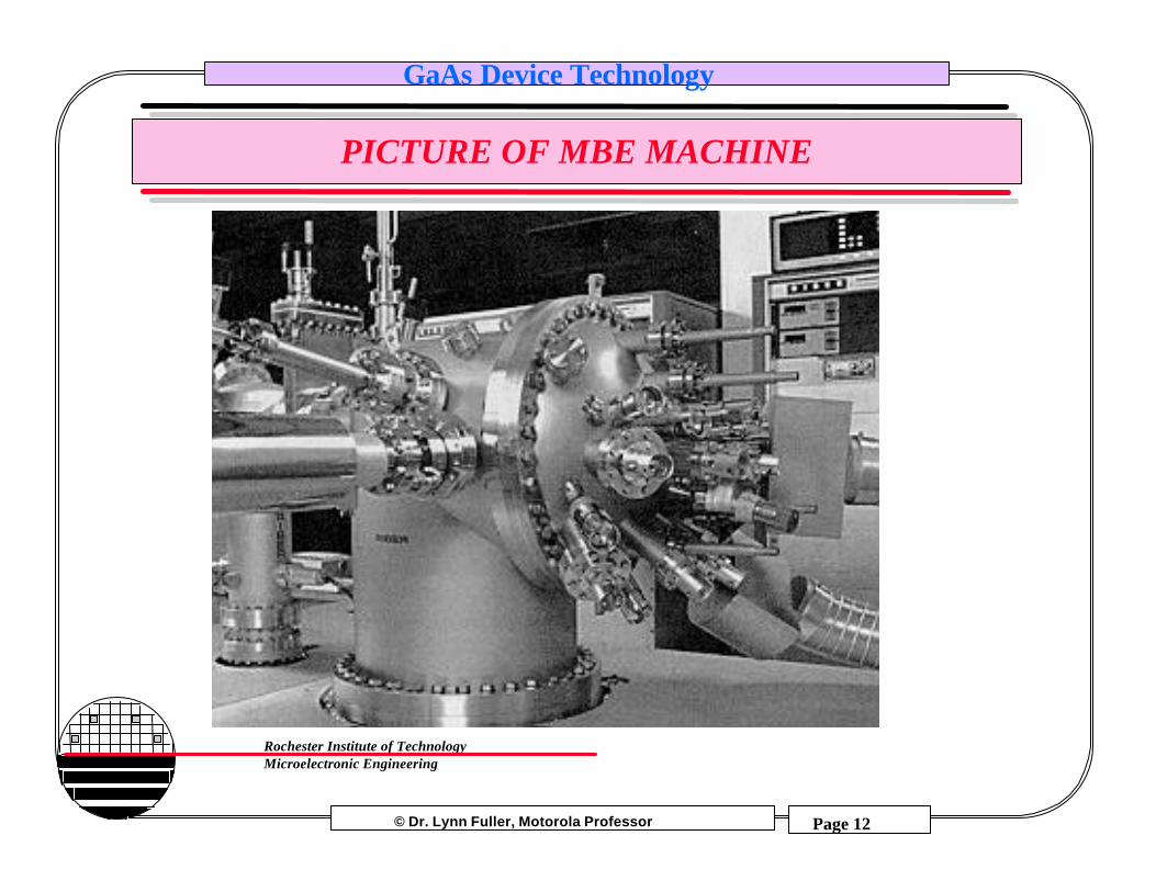
PICTURE OF MBE MACHINE
© Dr. Lynn Fuller, Motorola Professor
Rochester Institute of TechnologyMicroelectronic Engineering
GaAs Device Technology
Page 13
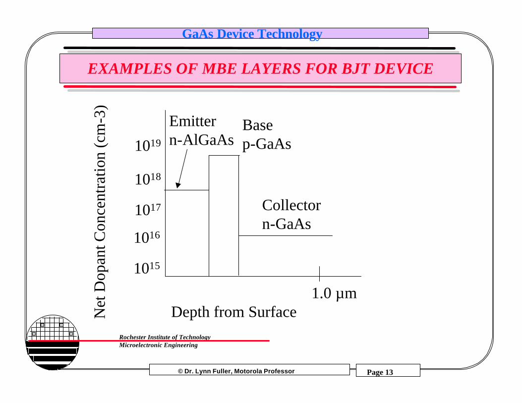
EXAMPLES OF MBE LAYERS FOR BJT DEVICE
1015
1019
1018
1017
1016
Collectorn-GaAs
Basep-GaAs
Emittern-AlGaAs
1.0 µmDepth from SurfaceN
et D
opan
t Con
cent
ratio
n (c
m-3
)
© Dr. Lynn Fuller, Motorola Professor
Rochester Institute of TechnologyMicroelectronic Engineering
GaAs Device Technology
Page 14
METAL CONTACTS TO GaAs
Aluminum makes a schottky barrier contact (rectifying) to n-typeGaAs.
Ohmic contacts are usually made using and alloyed (heated above theeutectic temperature) contact of Gold (Au) and Germanium (Ge)followed by a layer of Nickel (Ni) and alloyed at a temperature abovethe AuGe eutectic temperature of 356 C. During alloying the Gedopes the surface of the GaAs n+
© Dr. Lynn Fuller, Motorola Professor
Rochester Institute of TechnologyMicroelectronic Engineering
GaAs Device Technology
Page 15
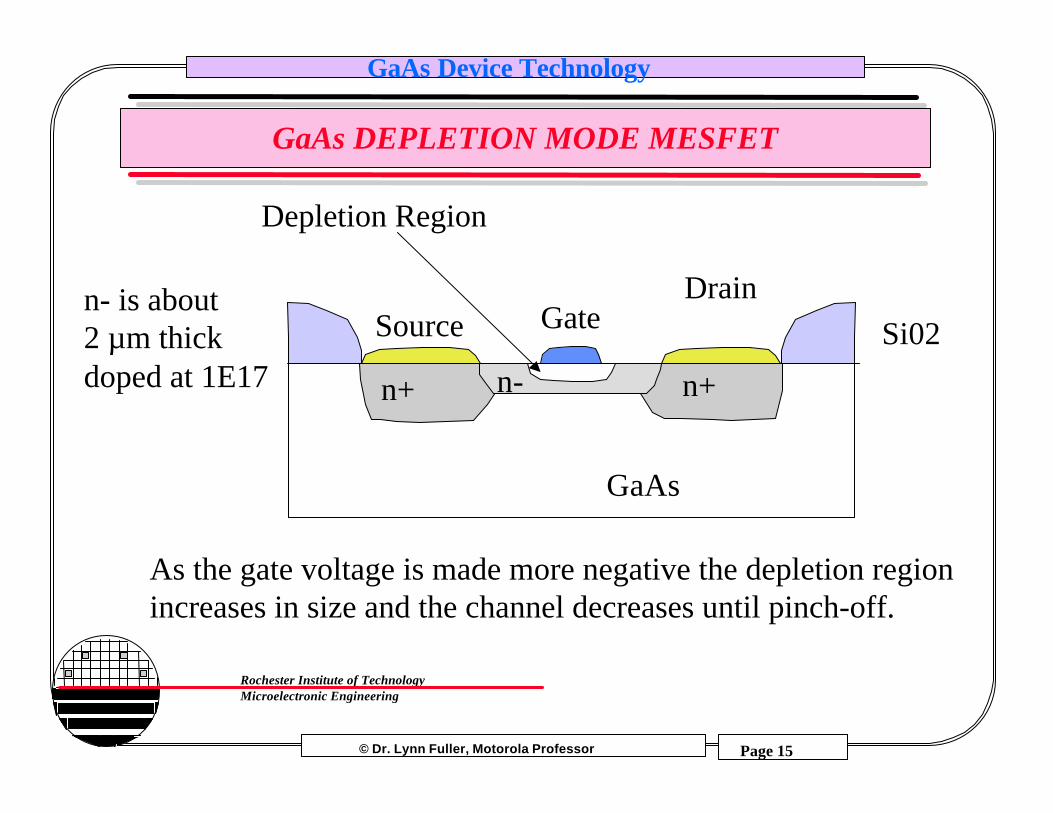
GaAs DEPLETION MODE MESFET
GaAs
n+n+
GateDrain
Source
n-
Depletion Region
n- is about 2 µm thickdoped at 1E17
Si02
As the gate voltage is made more negative the depletion regionincreases in size and the channel decreases until pinch-off.
© Dr. Lynn Fuller, Motorola Professor
Rochester Institute of TechnologyMicroelectronic Engineering
GaAs Device Technology
Page 16
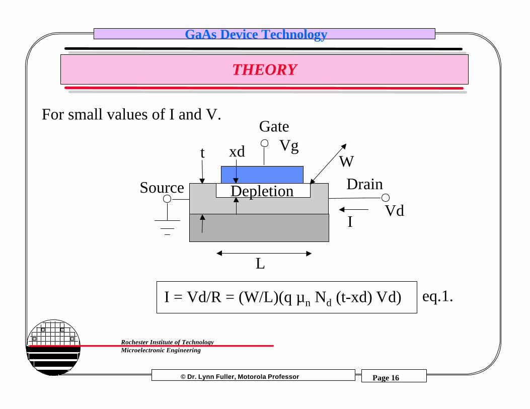
THEORY
Gate
Source Drain
L
I
Wt
I = Vd/R = (W/L)(q µn Nd (t-xd) Vd)
xd
Vd
For small values of I and V.
eq.1.
Depletion
Vg
© Dr. Lynn Fuller, Motorola Professor
Rochester Institute of TechnologyMicroelectronic Engineering
GaAs Device Technology
Page 17
THEORY
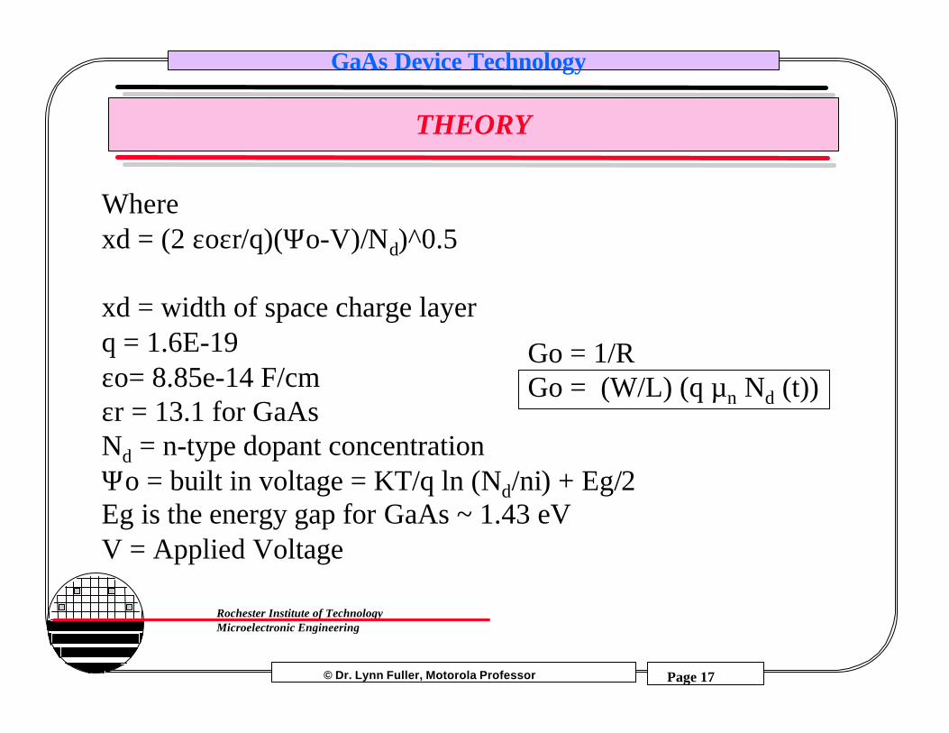
Wherexd = (2 εoεr/q)(Ψo-V)/Nd)^0.5
xd = width of space charge layerq = 1.6E-19εo= 8.85e-14 F/cmεr = 13.1 for GaAsNd = n-type dopant concentrationΨo = built in voltage = KT/q ln (Nd/ni) + Eg/2Eg is the energy gap for GaAs ~ 1.43 eVV = Applied Voltage
Go = 1/RGo = (W/L) (q µn Nd (t))
© Dr. Lynn Fuller, Motorola Professor
Rochester Institute of TechnologyMicroelectronic Engineering
GaAs Device Technology
Page 18
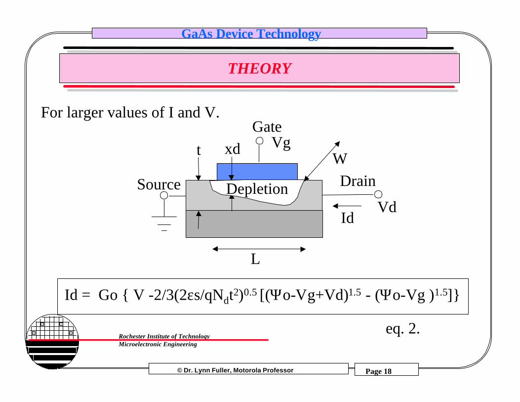
THEORY
Gate
Source Drain
L
Id
Wt xd
Vd
For larger values of I and V.
Depletion
Id = Go { V -2/3(2εs/qNdt2)0.5 [(Ψo-Vg+Vd)1.5 - (Ψo-Vg )1.5]}
Vg
eq. 2.
© Dr. Lynn Fuller, Motorola Professor
Rochester Institute of TechnologyMicroelectronic Engineering
GaAs Device Technology
Page 19
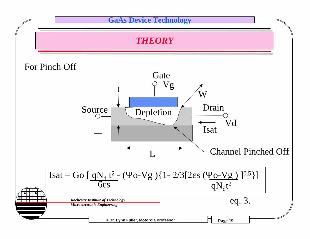
THEORY
Gate
Source Drain
L
Isat
Wt
Vd
For Pinch Off
Channel Pinched Off
Isat = Go [ qNd t2 - (Ψo-Vg ){1- 2/3[2εs (Ψo-Vg ) ]0.5}]
Depletion
Vg
qNdt26εs
eq. 3.
© Dr. Lynn Fuller, Motorola Professor
Rochester Institute of TechnologyMicroelectronic Engineering
GaAs Device Technology
Page 20
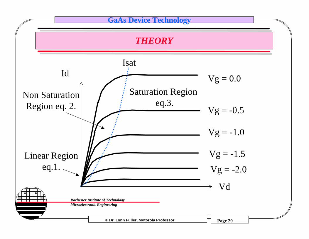
THEORY
Vd
Id Vg = 0.0
Vg = -2.0
Vg = -1.5
Vg = -0.5
Vg = -1.0
Saturation Region eq.3.
Non SaturationRegion eq. 2.
Linear Regioneq.1.
Isat
© Dr. Lynn Fuller, Motorola Professor
Rochester Institute of TechnologyMicroelectronic Engineering
GaAs Device Technology
Page 21
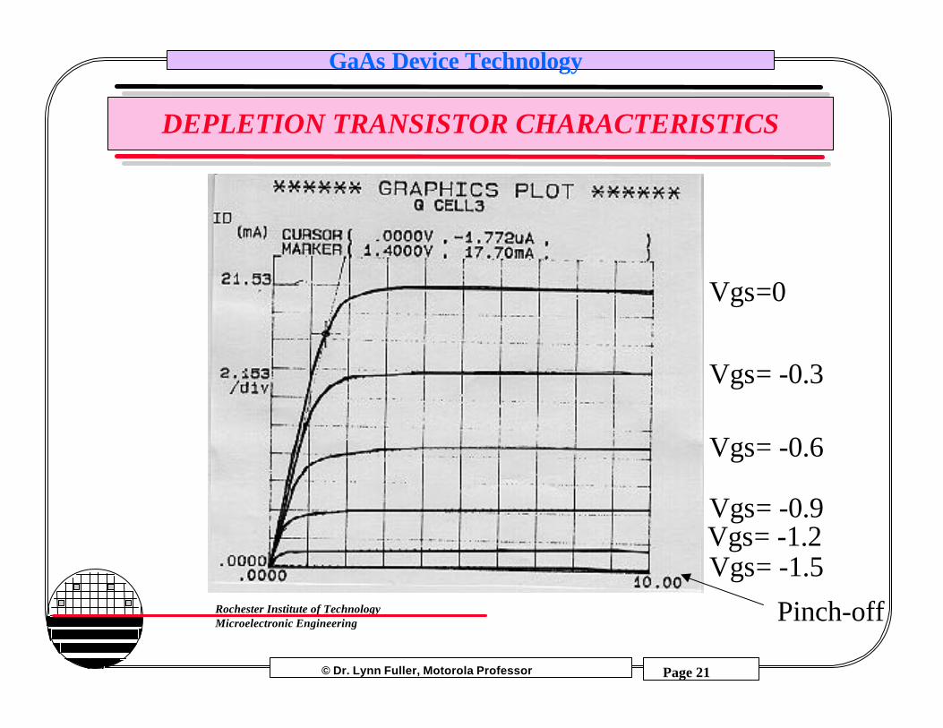
DEPLETION TRANSISTOR CHARACTERISTICS
Vgs=0
Vgs= -0.6
Vgs= -0.3
Vgs= -0.9Vgs= -1.2Vgs= -1.5
Pinch-off
© Dr. Lynn Fuller, Motorola Professor
Rochester Institute of TechnologyMicroelectronic Engineering
GaAs Device Technology
Page 22
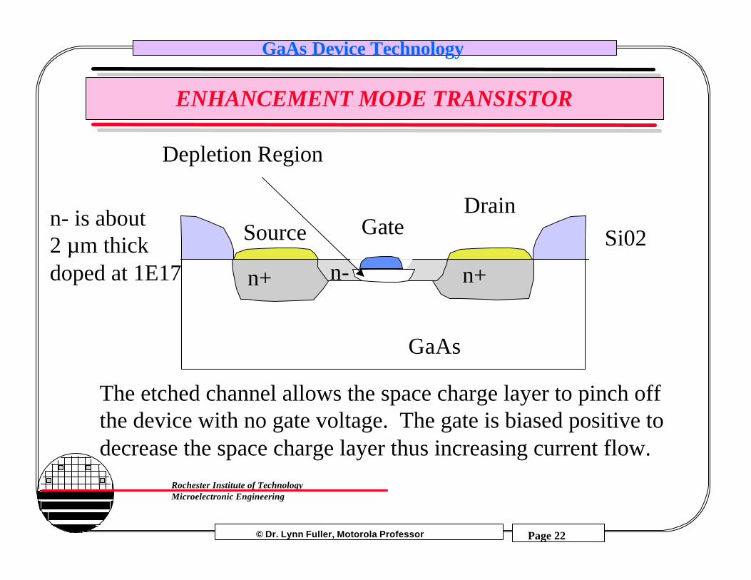
ENHANCEMENT MODE TRANSISTOR
GaAs
n+n+
GateDrain
Source
n-
Depletion Region
Si02n- is about 2 µm thickdoped at 1E17
The etched channel allows the space charge layer to pinch offthe device with no gate voltage. The gate is biased positive todecrease the space charge layer thus increasing current flow.
© Dr. Lynn Fuller, Motorola Professor
Rochester Institute of TechnologyMicroelectronic Engineering
GaAs Device Technology
Page 23
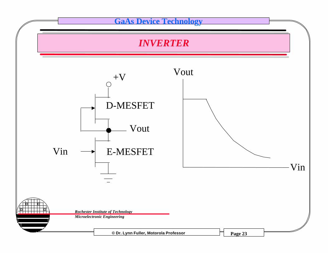
INVERTER
Vout
+V
Vin
D-MESFET
E-MESFET
Vout
Vin
© Dr. Lynn Fuller, Motorola Professor
Rochester Institute of TechnologyMicroelectronic Engineering
GaAs Device Technology
Page 24
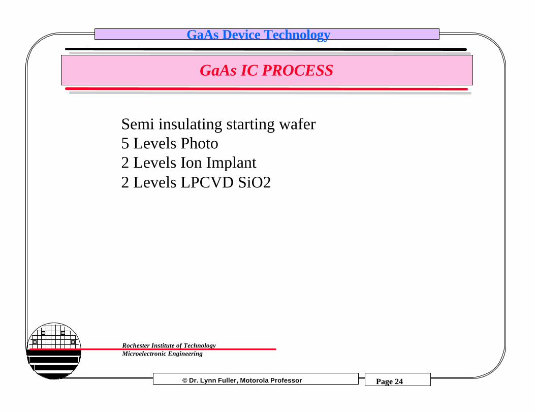
GaAs IC PROCESS
Semi insulating starting wafer5 Levels Photo2 Levels Ion Implant2 Levels LPCVD SiO2
© Dr. Lynn Fuller, Motorola Professor
Rochester Institute of TechnologyMicroelectronic Engineering
GaAs Device Technology
Page 25
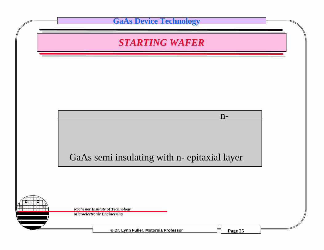
STARTING WAFER
GaAs semi insulating with n- epitaxial layer
n-
© Dr. Lynn Fuller, Motorola Professor
Rochester Institute of TechnologyMicroelectronic Engineering
GaAs Device Technology
Page 26
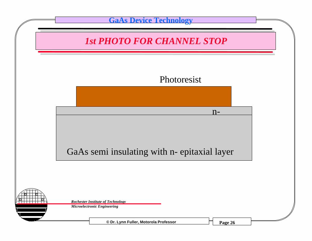
1st PHOTO FOR CHANNEL STOP
Photoresist
GaAs semi insulating with n- epitaxial layer
n-
© Dr. Lynn Fuller, Motorola Professor
Rochester Institute of TechnologyMicroelectronic Engineering
GaAs Device Technology
Page 27
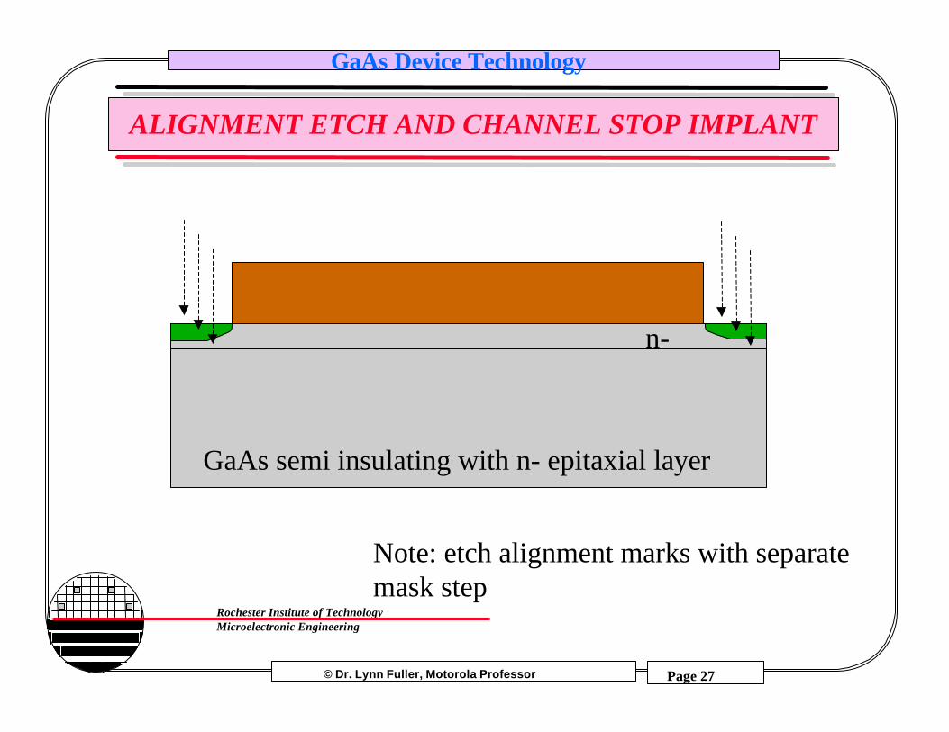
ALIGNMENT ETCH AND CHANNEL STOP IMPLANT
GaAs semi insulating with n- epitaxial layer
n-
Note: etch alignment marks with separatemask step
© Dr. Lynn Fuller, Motorola Professor
Rochester Institute of TechnologyMicroelectronic Engineering
GaAs Device Technology
Page 28
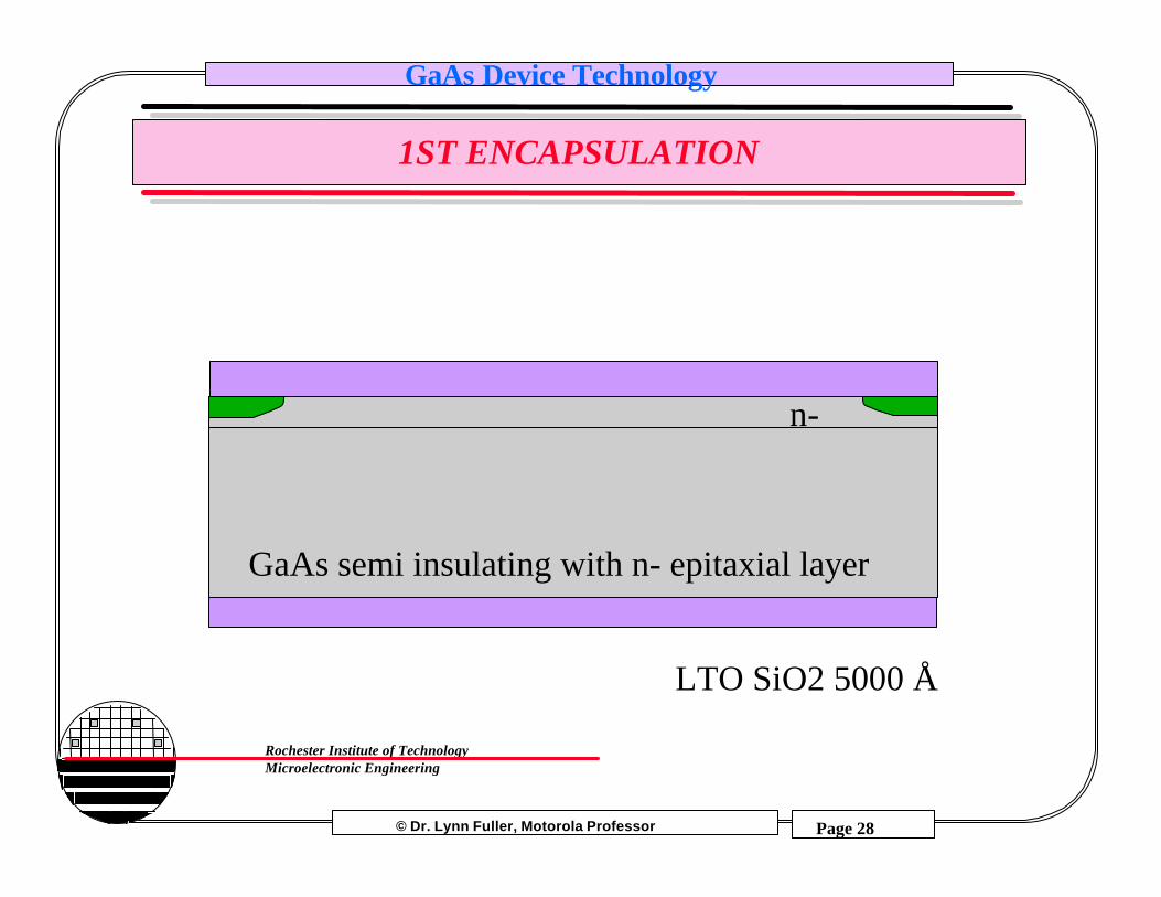
1ST ENCAPSULATION
LTO SiO2 5000 Å
GaAs semi insulating with n- epitaxial layer
n-
© Dr. Lynn Fuller, Motorola Professor
Rochester Institute of TechnologyMicroelectronic Engineering
GaAs Device Technology
Page 29
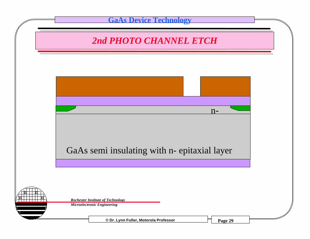
2nd PHOTO CHANNEL ETCH
GaAs semi insulating with n- epitaxial layer
n-
© Dr. Lynn Fuller, Motorola Professor
Rochester Institute of TechnologyMicroelectronic Engineering
GaAs Device Technology
Page 30
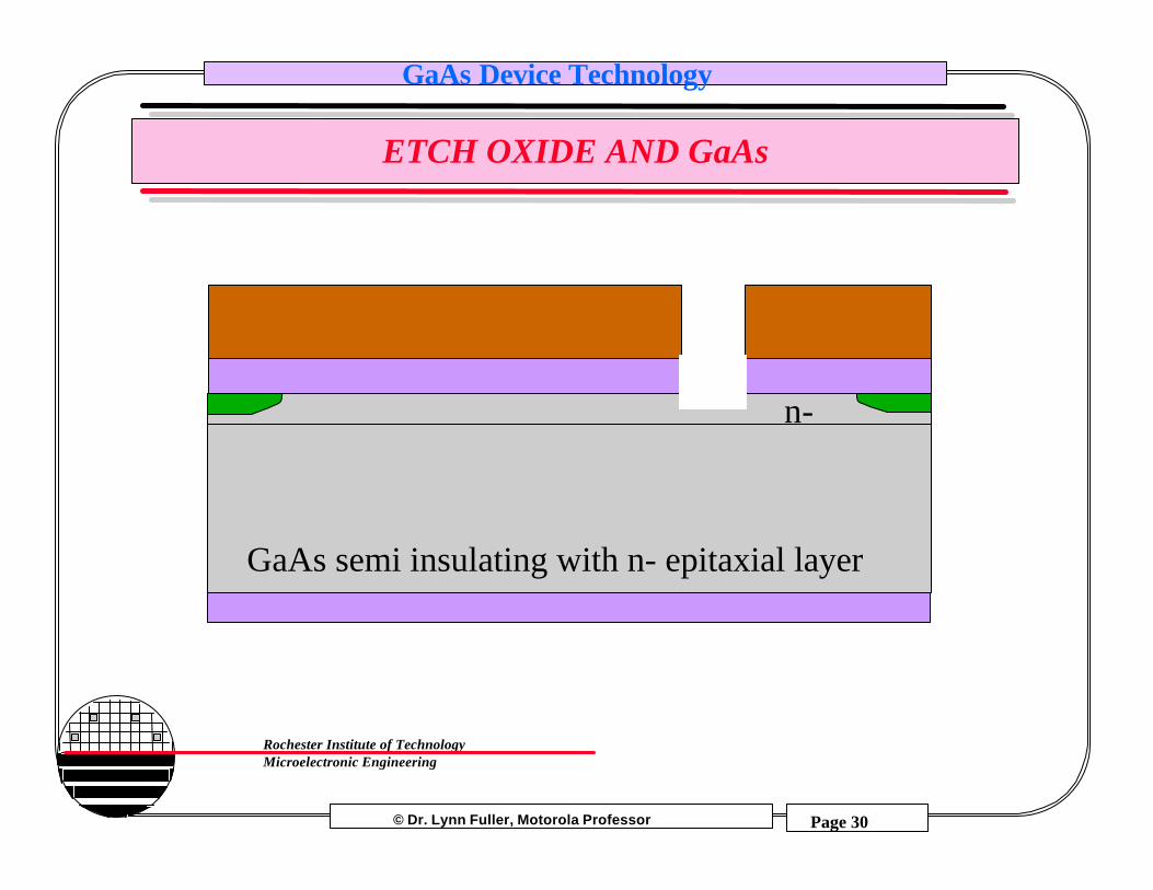
ETCH OXIDE AND GaAs
GaAs semi insulating with n- epitaxial layer
n-
© Dr. Lynn Fuller, Motorola Professor
Rochester Institute of TechnologyMicroelectronic Engineering
GaAs Device Technology
Page 31
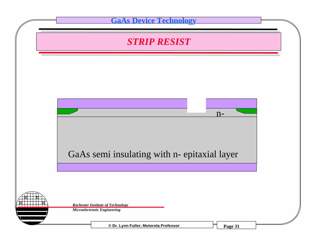
STRIP RESIST
GaAs semi insulating with n- epitaxial layer
n-
© Dr. Lynn Fuller, Motorola Professor
Rochester Institute of TechnologyMicroelectronic Engineering
GaAs Device Technology
Page 32
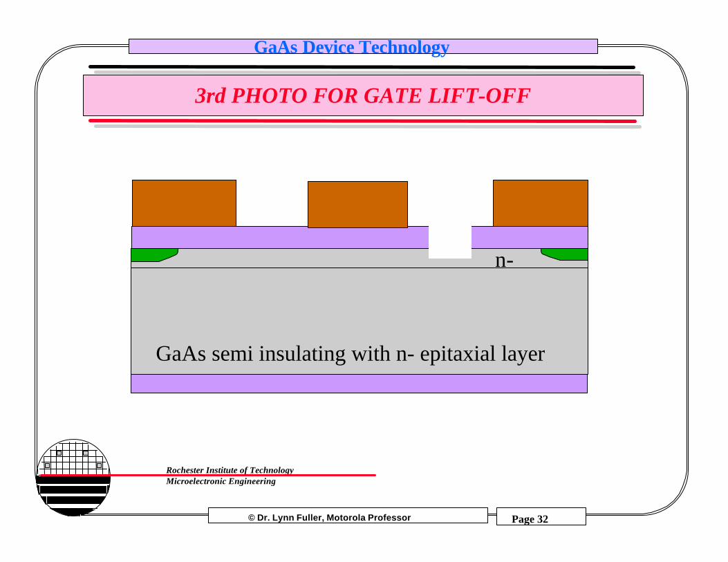
3rd PHOTO FOR GATE LIFT-OFF
GaAs semi insulating with n- epitaxial layer
n-
© Dr. Lynn Fuller, Motorola Professor
Rochester Institute of TechnologyMicroelectronic Engineering
GaAs Device Technology
Page 33
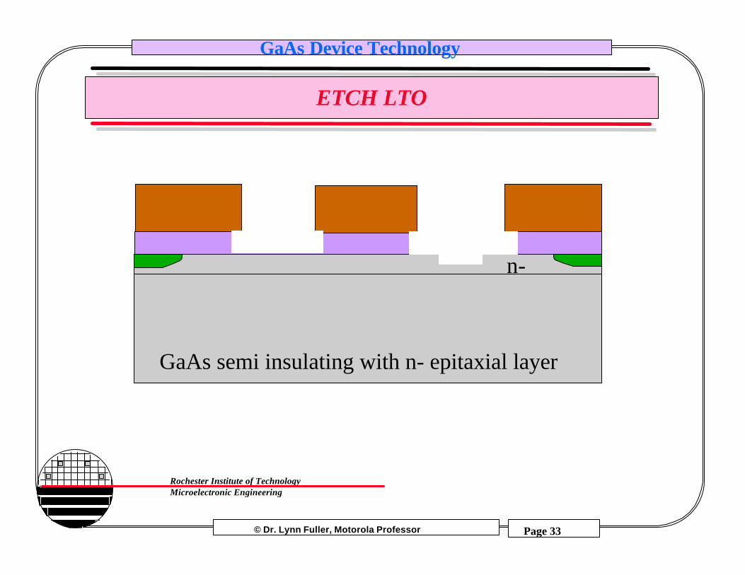
ETCH LTO
GaAs semi insulating with n- epitaxial layer
n-
© Dr. Lynn Fuller, Motorola Professor
Rochester Institute of TechnologyMicroelectronic Engineering
GaAs Device Technology
Page 34
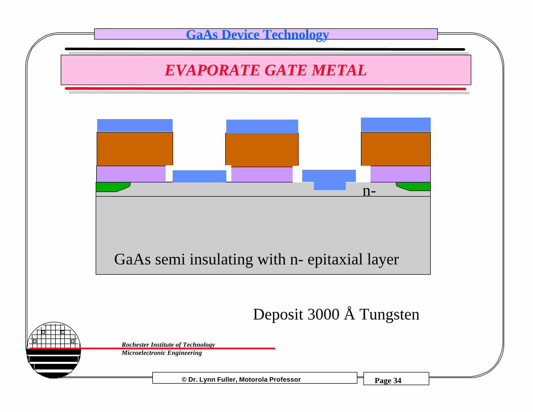
EVAPORATE GATE METAL
GaAs semi insulating with n- epitaxial layer
n-
Deposit 3000 Å Tungsten
© Dr. Lynn Fuller, Motorola Professor
Rochester Institute of TechnologyMicroelectronic Engineering
GaAs Device Technology
Page 35
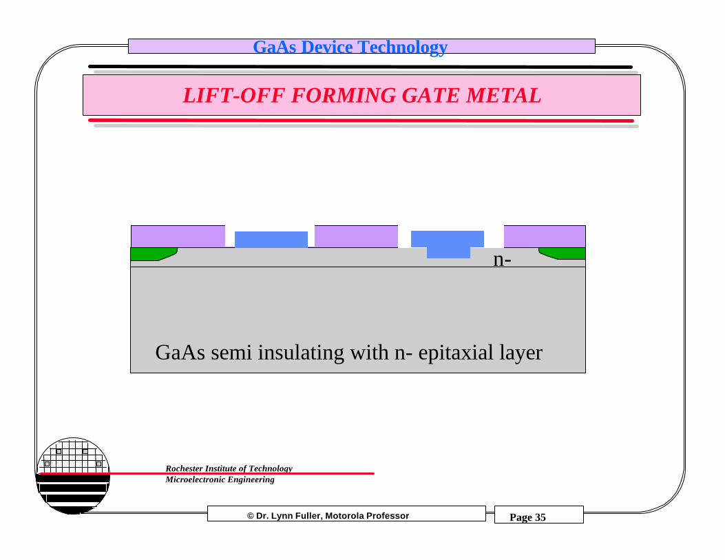
LIFT-OFF FORMING GATE METAL
GaAs semi insulating with n- epitaxial layer
n-
© Dr. Lynn Fuller, Motorola Professor
Rochester Institute of TechnologyMicroelectronic Engineering
GaAs Device Technology
Page 36
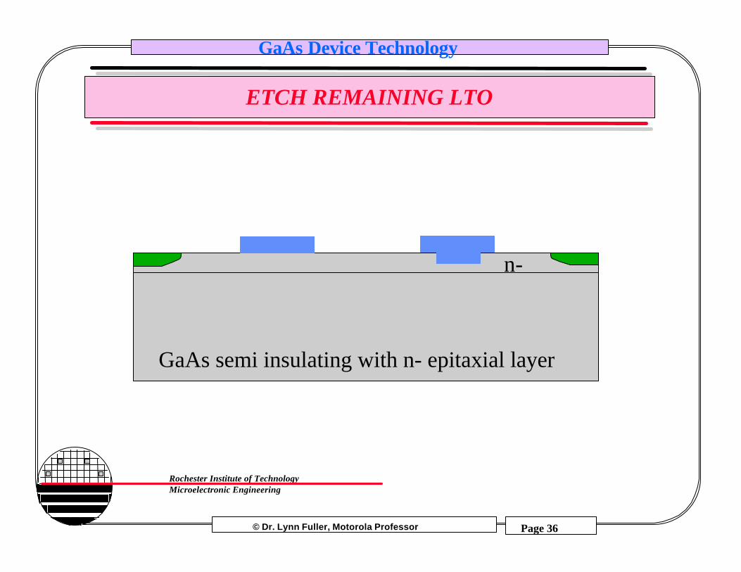
ETCH REMAINING LTO
GaAs semi insulating with n- epitaxial layer
n-
© Dr. Lynn Fuller, Motorola Professor
Rochester Institute of TechnologyMicroelectronic Engineering
GaAs Device Technology
Page 37
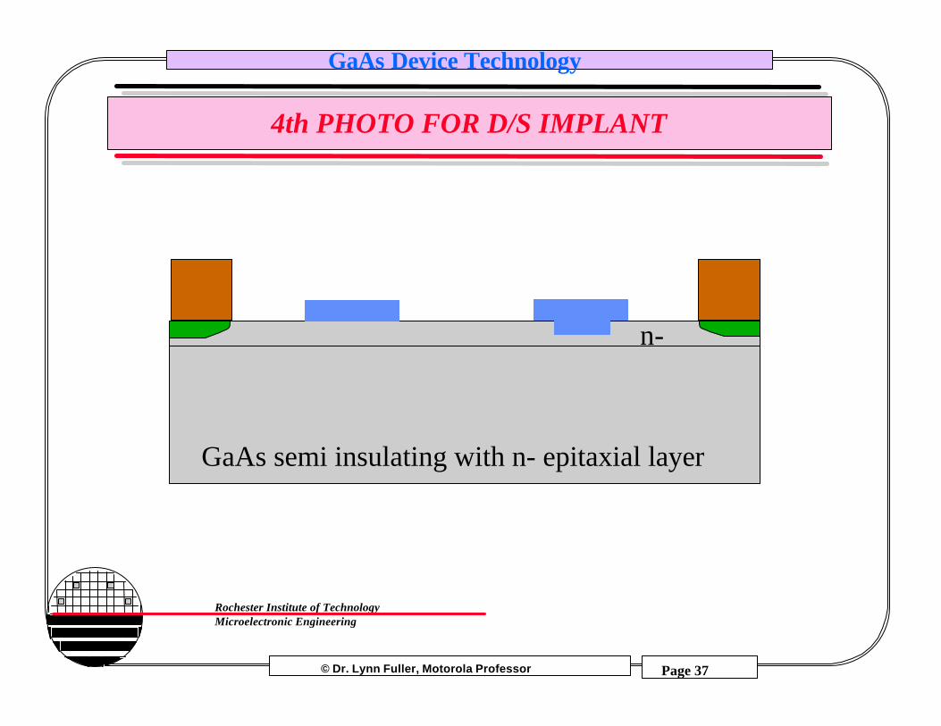
4th PHOTO FOR D/S IMPLANT
GaAs semi insulating with n- epitaxial layer
n-
© Dr. Lynn Fuller, Motorola Professor
Rochester Institute of TechnologyMicroelectronic Engineering
GaAs Device Technology
Page 38
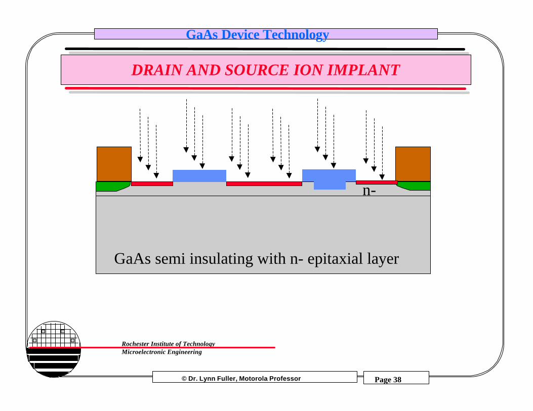
DRAIN AND SOURCE ION IMPLANT
GaAs semi insulating with n- epitaxial layer
n-
© Dr. Lynn Fuller, Motorola Professor
Rochester Institute of TechnologyMicroelectronic Engineering
GaAs Device Technology
Page 39
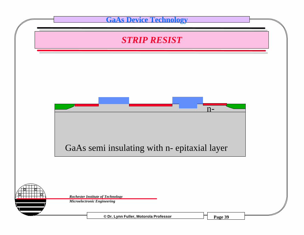
STRIP RESIST
GaAs semi insulating with n- epitaxial layer
n-
© Dr. Lynn Fuller, Motorola Professor
Rochester Institute of TechnologyMicroelectronic Engineering
GaAs Device Technology
Page 40
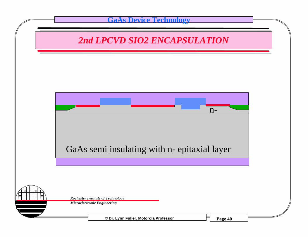
2nd LPCVD SIO2 ENCAPSULATION
GaAs semi insulating with n- epitaxial layer
n-
© Dr. Lynn Fuller, Motorola Professor
Rochester Institute of TechnologyMicroelectronic Engineering
GaAs Device Technology
Page 41
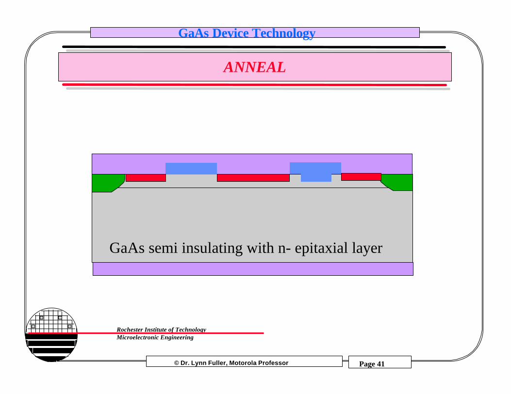
ANNEAL
GaAs semi insulating with n- epitaxial layer
© Dr. Lynn Fuller, Motorola Professor
Rochester Institute of TechnologyMicroelectronic Engineering
GaAs Device Technology
Page 42
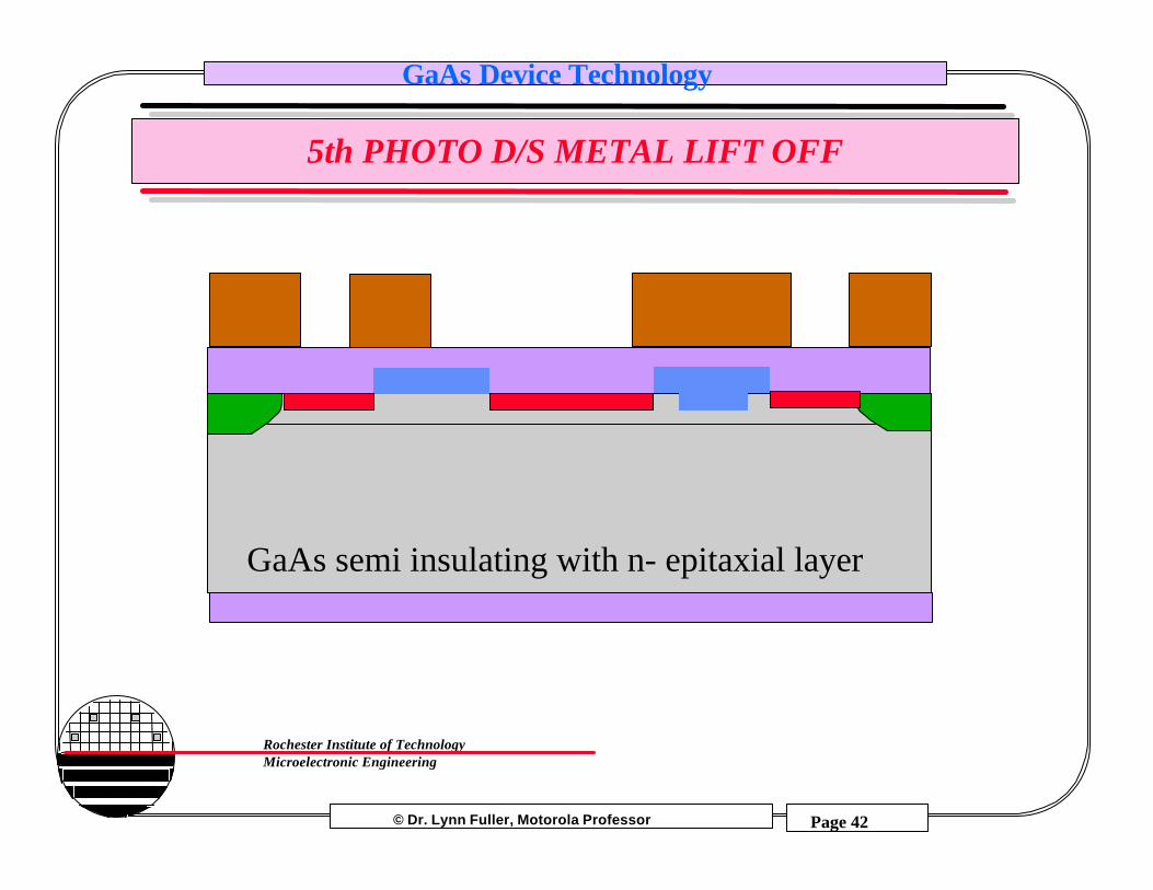
5th PHOTO D/S METAL LIFT OFF
GaAs semi insulating with n- epitaxial layer
© Dr. Lynn Fuller, Motorola Professor
Rochester Institute of TechnologyMicroelectronic Engineering
GaAs Device Technology
Page 43
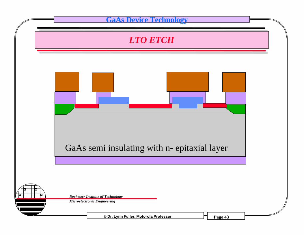
LTO ETCH
GaAs semi insulating with n- epitaxial layer
© Dr. Lynn Fuller, Motorola Professor
Rochester Institute of TechnologyMicroelectronic Engineering
GaAs Device Technology
Page 44
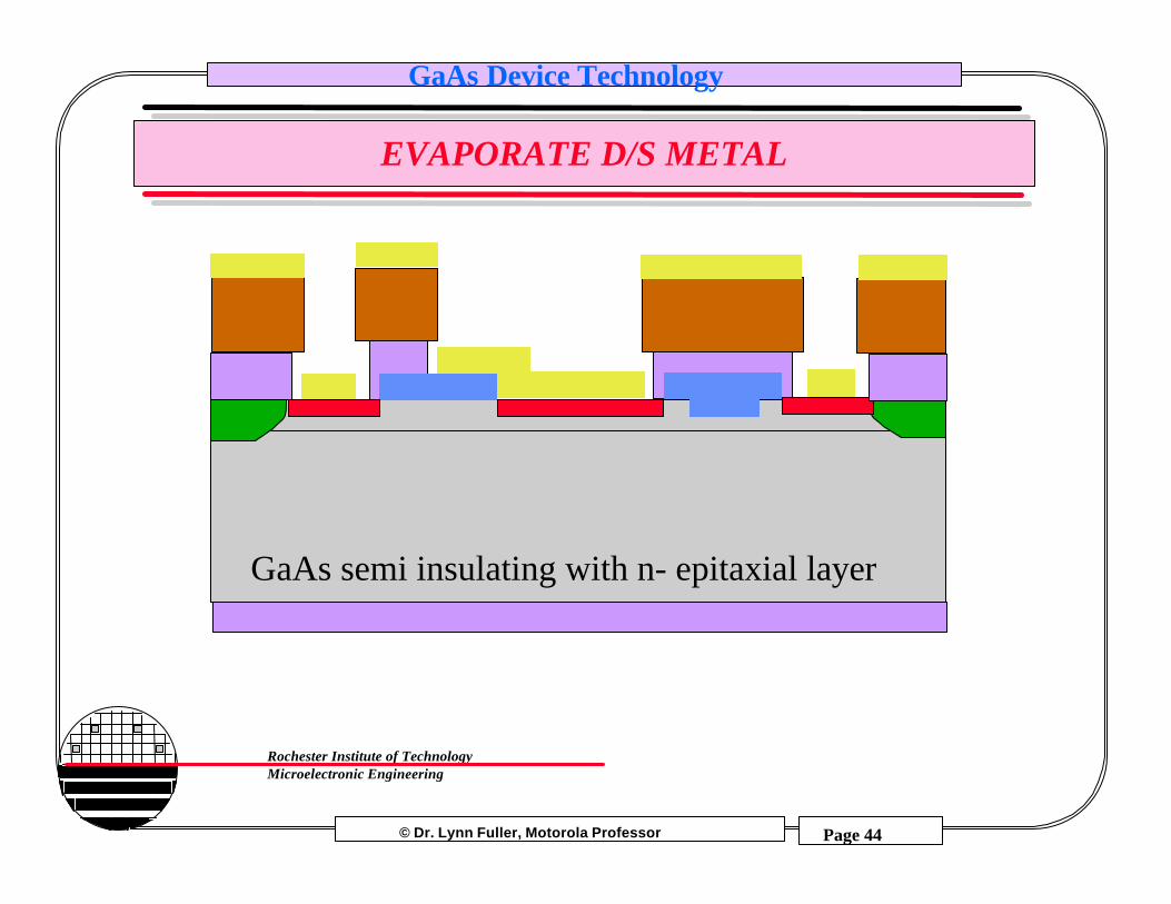
EVAPORATE D/S METAL
GaAs semi insulating with n- epitaxial layer
© Dr. Lynn Fuller, Motorola Professor
Rochester Institute of TechnologyMicroelectronic Engineering
GaAs Device Technology
Page 45
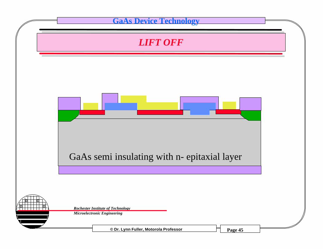
LIFT OFF
GaAs semi insulating with n- epitaxial layer
© Dr. Lynn Fuller, Motorola Professor
Rochester Institute of TechnologyMicroelectronic Engineering
GaAs Device Technology
Page 46
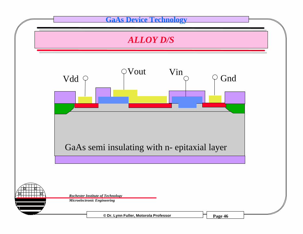
ALLOY D/S
GaAs semi insulating with n- epitaxial layer
VddVout Vin
Gnd
© Dr. Lynn Fuller, Motorola Professor
Rochester Institute of TechnologyMicroelectronic Engineering
GaAs Device Technology
Page 47
SUMMARY
GaAs has higher electron mobility giving devices with improvedradio frequency performance or higher speed digital devices.
GaAs has different processing technology from silicon ICtechnology including: MBE, no oxide growth, encapsulation toprevent loss of arsenic at temperatures above 400 C.
The main semiconductor device made is the MESFET.
Optical LEDs and LASERs can be made in GaAs or related III-Vsemiconductors.
© Dr. Lynn Fuller, Motorola Professor
Rochester Institute of TechnologyMicroelectronic Engineering
GaAs Device Technology
Page 48
REFERENCES
1. “A Comparison of GaAs and Si Processing Technology”, C.E.Weitzel, J.M. Frary, Motorola Semiconductor Research andDevelopment Labs, Semiconductor International, June 19822. “GaAs Ics Bid for Commercial Success”, Larry Waller,Electronics June 14, 1984.3.3. GaAs no longer next year’s technology as digital circuits come tomarket”, W. Twaddell, EDN May 17, 1984.4. “Are MMICs a Fad or Fact”, D.R. Decker, MSN, July 1983.5. “Gallium Arsenide”, Inside Technology Today - a TexasInstruments Videotape Series, 18 min.
© Dr. Lynn Fuller, Motorola Professor
Rochester Institute of TechnologyMicroelectronic Engineering
GaAs Device Technology
Page 49
HOMEWORK - GaAs
1. Sketch the layout of a GaAs inverter built using the fabricationprocess described.2. Why are direct gap semiconductor materials necessary forlight emitting devices.3. What energy gap corresponds to 600 nm (red) and 400 nm(blue).