Embed Size (px)
Citation preview

Generic Flash Programmer UserGuideIntel® Quartus® Prime Standard Edition
Updated for Intel® Quartus® Prime Design Suite: 18.1.1
SubscribeSend Feedback
UG-20235 | 2019.05.15Latest document on the web: PDF | HTML
Contents
1. Generic Flash Programmer User Guide Intel® Quartus® Prime Standard Edition.............31.1. Supported Devices and Configuration Methods...........................................................41.2. Quad SPI Flash Byte-Addressing.............................................................................. 41.3. Generic Flash Programmer Operation....................................................................... 5
1.3.1. Generic Flash Programming (Convert Programming File Dialog Box)................. 51.3.2. Erasing Flash Memory Sectors................................................................... 14
1.4. Generic Flash Programmer Flow Templates (Convert Programming File).......................151.4.1. Initialization Flow Templates (Convert Programming File).............................. 151.4.2. Program Flow Template (Convert Programming File)..................................... 161.4.3. Erase Flow Template (Convert Programming File)......................................... 171.4.4. Verify/Blank-Check/Examine Flow Template (Convert Programming File)......... 181.4.5. Termination Flow Template (Convert Programming File).................................191.4.6. Programming Flow Action Properties...........................................................20
1.5. Generic Flash Programmer Settings Reference......................................................... 221.5.1. Convert Programming File Dialog Box......................................................... 231.5.2. Device and Pin Options............................................................................. 231.5.3. Compression and Encryption Settings (Convert Programming File)..................261.5.4. SOF Data Properties Dialog Box (Convert Programming File)..........................27
1.6. Generic Flash Programmer User Guide Revision History.............................................27
Contents
Generic Flash Programmer User Guide: Intel Quartus Prime Standard Edition Send Feedback
2
1. Generic Flash Programmer User Guide Intel® Quartus®
Prime Standard EditionThis document describes how to use the Generic Flash Programmer. You can use theGeneric Flash Programmer to load an FPGA configuration bitstream file into a QuadSPI flash memory device. The Quad SPI flash memory device subsequently loads theconfiguration data into the target FPGA via Active Serial (AS) configuration. You canoptionally enable bitstream compression and encryption security to reduce the sizeand protect the configuration bitstream files.
Figure 1. Generic Flash Programmer Configuration Example
Intel FPGA
Quad SPI Flash Memory
Intel FPGADownload Cable
PCB10 pin JTAG header
Intel Quartus PrimeProgrammer
FPGA Configuration and Flash Programming Data
10 pin
JIC File Programming
ASConfiguration
The Generic Flash Programmer allows you to send configuration data over a downloadcable via a JTAG connection to the target FPGA device. The target FPGA then in turnwrites the configuration data to the flash memory device. The AS configurationscheme loads the configuration data from the flash memory into the FPGA. Forexample, this method allows you to configure or reconfigure the FPGA from the flashmemory after restoring power to the FPGA after power down.
Related Information
• Intel® Arria® 10 Core Fabric and General Purpose I/Os Handbook
• Cyclone® V Device Handbook: Volume 1: Device Interfaces and Integration
• Configuration and Remote System Upgrades in Cyclone IV Devices
• Arria II Device Handbook
• Arria V Device Handbook: Volume 1: Device Interfaces and Integration
• Configuring Stratix® III Devices
UG-20235 | 2019.05.15
Send Feedback
Intel Corporation. All rights reserved. Agilex, Altera, Arria, Cyclone, Enpirion, Intel, the Intel logo, MAX, Nios,Quartus and Stratix words and logos are trademarks of Intel Corporation or its subsidiaries in the U.S. and/orother countries. Intel warrants performance of its FPGA and semiconductor products to current specifications inaccordance with Intel's standard warranty, but reserves the right to make changes to any products and servicesat any time without notice. Intel assumes no responsibility or liability arising out of the application or use of anyinformation, product, or service described herein except as expressly agreed to in writing by Intel. Intelcustomers are advised to obtain the latest version of device specifications before relying on any publishedinformation and before placing orders for products or services.*Other names and brands may be claimed as the property of others.
ISO9001:2015Registered
• Configuration, Design Security, Remote System Upgrades with Stratix® IV Devices
• Intel® Quartus® Prime Standard Edition User Guide: Programmer
1.1. Supported Devices and Configuration Methods
The Intel® Quartus® Prime Standard Edition Generic Flash Programmer supports thefollowing FPGA and flash memory devices and configuration methods.
Table 1. Generic Flash Programmer Device and Configuration Method Support (IntelQuartus Prime Standard Edition)
Supported Method
Supported Flash Programming InputFile
SRAM Object File (.sof)
Supported Flash Programming OutputFile
JTAG Indirect Configuration File (.jic)
Supported Configuration Schemes • Active Serial• Active Serial x4
Supported Devices Arria, Arria II, Arria V, Cyclone II, Cyclone III, Cyclone IV, Cyclone V, StratixII, Stratix III, Stratix IV, Stratix V, Intel Cyclone 10 LP, Intel Arria 10
1.2. Quad SPI Flash Byte-Addressing
Quad SPI flash devices typically support either 3-byte addressing, 4-byte addressing,or both for programming operations. You can only configure Intel FPGAs with a flashmemory device with byte addressing that is compatible with the Intel FPGA that youplan to configure.
The following table specifies the byte-addressing compatibility of Intel FPGAs forsupported flash memory devices:
Table 2. Intel FPGA Required Flash Memory Byte Addressing
FPGA Devices Required Flash Memory Byte Addressing
Intel Arria® 10 devices 4-byte addressing
Intel Cyclone® 10 LP devices 3-byte addressing
Arria V, Cyclone V, Stratix® V series devices • 3-byte addressing (limited memory address access(1))• 4-byte addressing
Cyclone IV, Cyclone II, Cyclone III, Arria GX, Arria II,Stratix II, Stratix III, Stratix IV, Stratix IV devices
3-byte addressing
(1) Flash devices that exceed 128 megabits (Mb) density require 4-byte addressing to access thememory space higher than 128 Mb. For flash devices that do not support non-volatile, 4-byteaddressing setting, the FPGA cannot read the configuration image that has a start addressbeyond 128Mb. For the remote system update application, the FPGA cannot store imagesbeyond 128Mb.
1. Generic Flash Programmer User Guide Intel® Quartus® Prime Standard Edition
UG-20235 | 2019.05.15
Generic Flash Programmer User Guide: Intel Quartus Prime Standard Edition Send Feedback
4
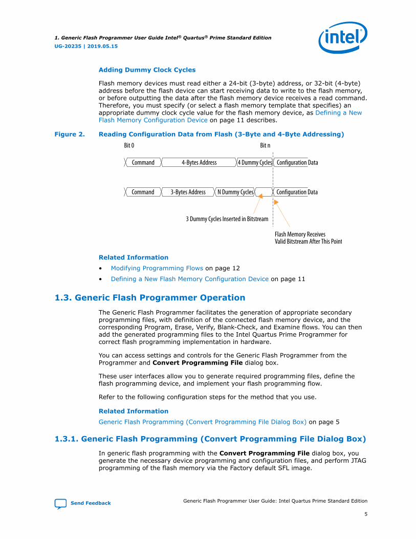
Adding Dummy Clock Cycles
Flash memory devices must read either a 24-bit (3-byte) address, or 32-bit (4-byte)address before the flash device can start receiving data to write to the flash memory,or before outputting the data after the flash memory device receives a read command.Therefore, you must specify (or select a flash memory template that specifies) anappropriate dummy clock cycle value for the flash memory device, as Defining a NewFlash Memory Configuration Device on page 11 describes.
Figure 2. Reading Configuration Data from Flash (3-Byte and 4-Byte Addressing)
Command 4-Bytes Address 4 Dummy Cycles Configuration Data
Command 3-Bytes Address N Dummy Cycles
3 Dummy Cycles Inserted in Bitstream
Flash Memory Receives Valid Bitstream After This Point
Configuration Data
Bit 0 Bit n
Related Information
• Modifying Programming Flows on page 12
• Defining a New Flash Memory Configuration Device on page 11
1.3. Generic Flash Programmer Operation
The Generic Flash Programmer facilitates the generation of appropriate secondaryprogramming files, with definition of the connected flash memory device, and thecorresponding Program, Erase, Verify, Blank-Check, and Examine flows. You can thenadd the generated programming files to the Intel Quartus Prime Programmer forcorrect flash programming implementation in hardware.
You can access settings and controls for the Generic Flash Programmer from theProgrammer and Convert Programming File dialog box.
These user interfaces allow you to generate required programming files, define theflash programming device, and implement your flash programming flow.
Refer to the following configuration steps for the method that you use.
Related Information
Generic Flash Programming (Convert Programming File Dialog Box) on page 5
1.3.1. Generic Flash Programming (Convert Programming File Dialog Box)
In generic flash programming with the Convert Programming File dialog box, yougenerate the necessary device programming and configuration files, and perform JTAGprogramming of the flash memory via the Factory default SFL image.
1. Generic Flash Programmer User Guide Intel® Quartus® Prime Standard Edition
UG-20235 | 2019.05.15
Send Feedback Generic Flash Programmer User Guide: Intel Quartus Prime Standard Edition
5
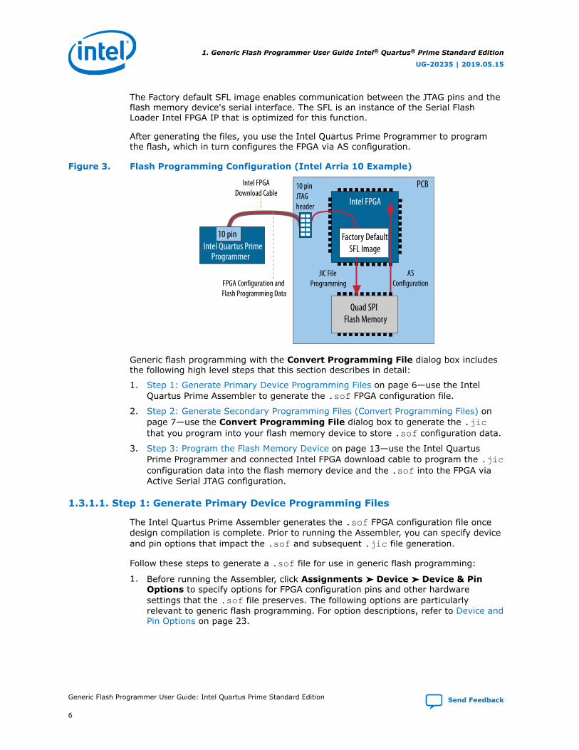
The Factory default SFL image enables communication between the JTAG pins and theflash memory device's serial interface. The SFL is an instance of the Serial FlashLoader Intel FPGA IP that is optimized for this function.
After generating the files, you use the Intel Quartus Prime Programmer to programthe flash, which in turn configures the FPGA via AS configuration.
Figure 3. Flash Programming Configuration (Intel Arria 10 Example)
Intel FPGA
Quad SPI Flash Memory
Intel FPGADownload Cable
PCB10 pin JTAG header
Intel Quartus PrimeProgrammer
FPGA Configuration and Flash Programming Data
Factory DefaultSFL Image
10 pin
JIC File Programming
ASConfiguration
Generic flash programming with the Convert Programming File dialog box includesthe following high level steps that this section describes in detail:
1. Step 1: Generate Primary Device Programming Files on page 6—use the IntelQuartus Prime Assembler to generate the .sof FPGA configuration file.
2. Step 2: Generate Secondary Programming Files (Convert Programming Files) onpage 7—use the Convert Programming File dialog box to generate the .jicthat you program into your flash memory device to store .sof configuration data.
3. Step 3: Program the Flash Memory Device on page 13—use the Intel QuartusPrime Programmer and connected Intel FPGA download cable to program the .jicconfiguration data into the flash memory device and the .sof into the FPGA viaActive Serial JTAG configuration.
1.3.1.1. Step 1: Generate Primary Device Programming Files
The Intel Quartus Prime Assembler generates the .sof FPGA configuration file oncedesign compilation is complete. Prior to running the Assembler, you can specify deviceand pin options that impact the .sof and subsequent .jic file generation.
Follow these steps to generate a .sof file for use in generic flash programming:
1. Before running the Assembler, click Assignments ➤ Device ➤ Device & PinOptions to specify options for FPGA configuration pins and other hardwaresettings that the .sof file preserves. The following options are particularlyrelevant to generic flash programming. For option descriptions, refer to Device andPin Options on page 23.
1. Generic Flash Programmer User Guide Intel® Quartus® Prime Standard Edition
UG-20235 | 2019.05.15
Generic Flash Programmer User Guide: Intel Quartus Prime Standard Edition Send Feedback
6
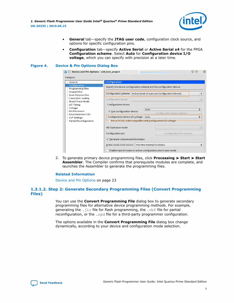
• General tab—specify the JTAG user code, configuration clock source, andoptions for specific configuration pins.
• Configuration tab—specify Active Serial or Active Serial x4 for the FPGAConfiguration scheme. Select Auto for Configuration device I/Ovoltage, which you can specify with precision at a later time.
Figure 4. Device & Pin Options Dialog Box
2. To generate primary device programming files, click Processing ➤ Start ➤ StartAssembler. The Compiler confirms that prerequisite modules are complete, andlaunches the Assembler to generate the programming files.
Related Information
Device and Pin Options on page 23
1.3.1.2. Step 2: Generate Secondary Programming Files (Convert ProgrammingFiles)
You can use the Convert Programming File dialog box to generate secondaryprogramming files for alternative device programming methods. For example,generating the .jic file for flash programming, the .rbf file for partialreconfiguration, or the .rpd file for a third-party programmer configuration.
The options available in the Convert Programming File dialog box changedynamically, according to your device and configuration mode selection.
1. Generic Flash Programmer User Guide Intel® Quartus® Prime Standard Edition
UG-20235 | 2019.05.15
Send Feedback Generic Flash Programmer User Guide: Intel Quartus Prime Standard Edition
7
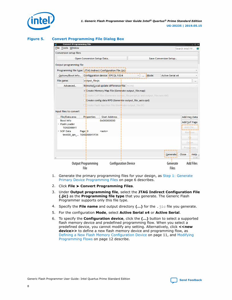
Figure 5. Convert Programming File Dialog Box
Configuration Device Add FilesGenerate Files
Output Programming File
1. Generate the primary programming files for your design, as Step 1: GeneratePrimary Device Programming Files on page 6 describes.
2. Click File ➤ Convert Programming Files.
3. Under Output programming file, select the JTAG Indirect Configuration File(.jic) as the Programming file type that you generate. The Generic FlashProgrammer supports only this file type.
4. Specify the File name and output directory (…) for the .jic file you generate.
5. For the configuration Mode, select Active Serial x4 or Active Serial.
6. To specify the Configuration device, click the (…) button to select a supportedflash memory device and predefined programming flow. When you select apredefined device, you cannot modify any setting. Alternatively, click <<newdevice>> to define a new flash memory device and programming flow, as Defining a New Flash Memory Configuration Device on page 11, and ModifyingProgramming Flows on page 12 describe.
1. Generic Flash Programmer User Guide Intel® Quartus® Prime Standard Edition
UG-20235 | 2019.05.15
Generic Flash Programmer User Guide: Intel Quartus Prime Standard Edition Send Feedback
8
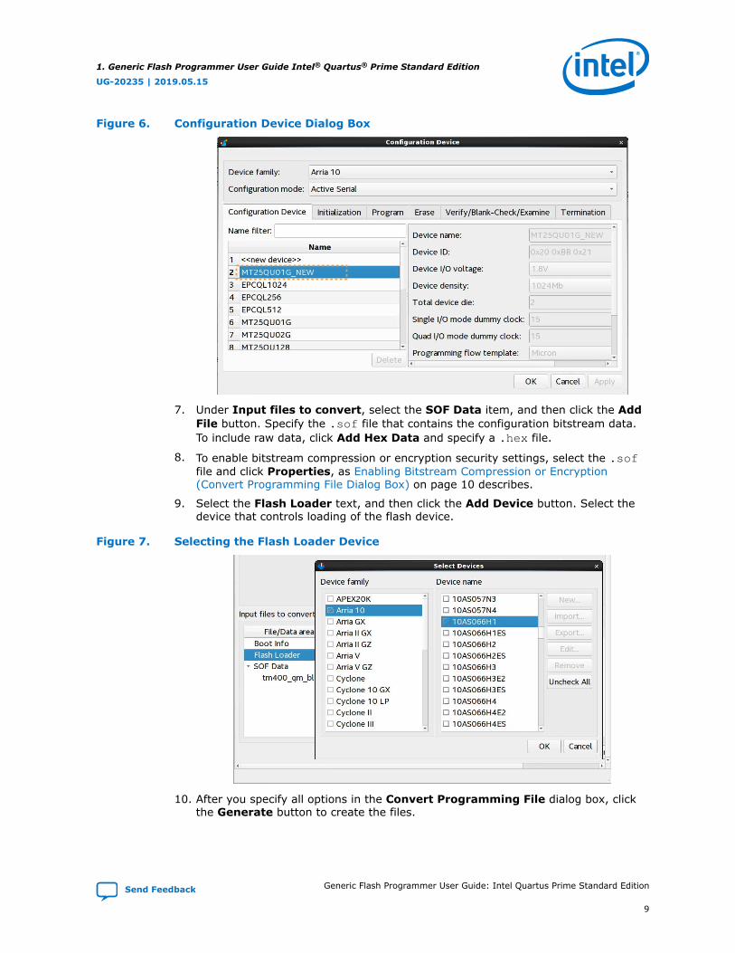
Figure 6. Configuration Device Dialog Box
7. Under Input files to convert, select the SOF Data item, and then click the AddFile button. Specify the .sof file that contains the configuration bitstream data.To include raw data, click Add Hex Data and specify a .hex file.
8. To enable bitstream compression or encryption security settings, select the .soffile and click Properties, as Enabling Bitstream Compression or Encryption(Convert Programming File Dialog Box) on page 10 describes.
9. Select the Flash Loader text, and then click the Add Device button. Select thedevice that controls loading of the flash device.
Figure 7. Selecting the Flash Loader Device
10. After you specify all options in the Convert Programming File dialog box, clickthe Generate button to create the files.
1. Generic Flash Programmer User Guide Intel® Quartus® Prime Standard Edition
UG-20235 | 2019.05.15
Send Feedback Generic Flash Programmer User Guide: Intel Quartus Prime Standard Edition
9
Related Information
• Defining a New Flash Memory Configuration Device on page 11
• Enabling Bitstream Compression or Encryption (Convert Programming File DialogBox) on page 10
• Modifying Programming Flows on page 12
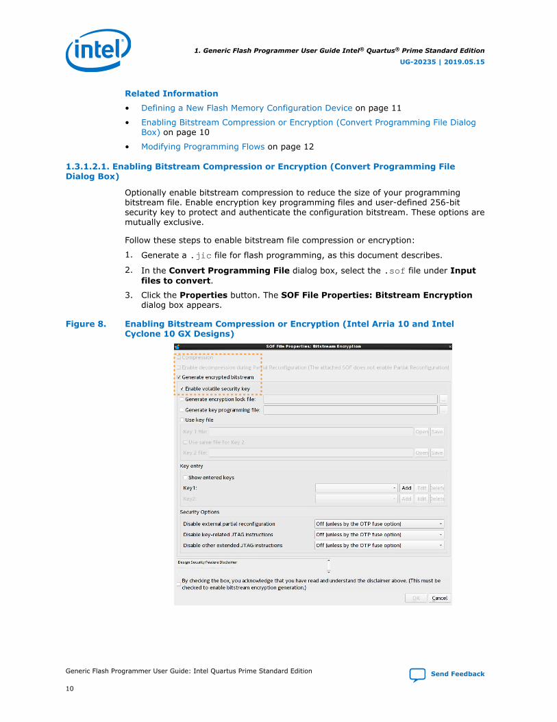
1.3.1.2.1. Enabling Bitstream Compression or Encryption (Convert Programming FileDialog Box)
Optionally enable bitstream compression to reduce the size of your programmingbitstream file. Enable encryption key programming files and user-defined 256-bitsecurity key to protect and authenticate the configuration bitstream. These options aremutually exclusive.
Follow these steps to enable bitstream file compression or encryption:
1. Generate a .jic file for flash programming, as this document describes.
2. In the Convert Programming File dialog box, select the .sof file under Inputfiles to convert.
3. Click the Properties button. The SOF File Properties: Bitstream Encryptiondialog box appears.
Figure 8. Enabling Bitstream Compression or Encryption (Intel Arria 10 and IntelCyclone 10 GX Designs)
1. Generic Flash Programmer User Guide Intel® Quartus® Prime Standard Edition
UG-20235 | 2019.05.15
Generic Flash Programmer User Guide: Intel Quartus Prime Standard Edition Send Feedback
10
4. To enable compression, turn on the Compression option. All encryption optionsdisable.
5. To enable bitstream file encryption:
a. Turn off the Compression option.
b. Turn on the Generate encrypted bitstream option.
c. Specify options for programming file key decryption, and Security Options,as Compression and Encryption Settings (Convert Programming File) on page26 describes.
6. Click OK.
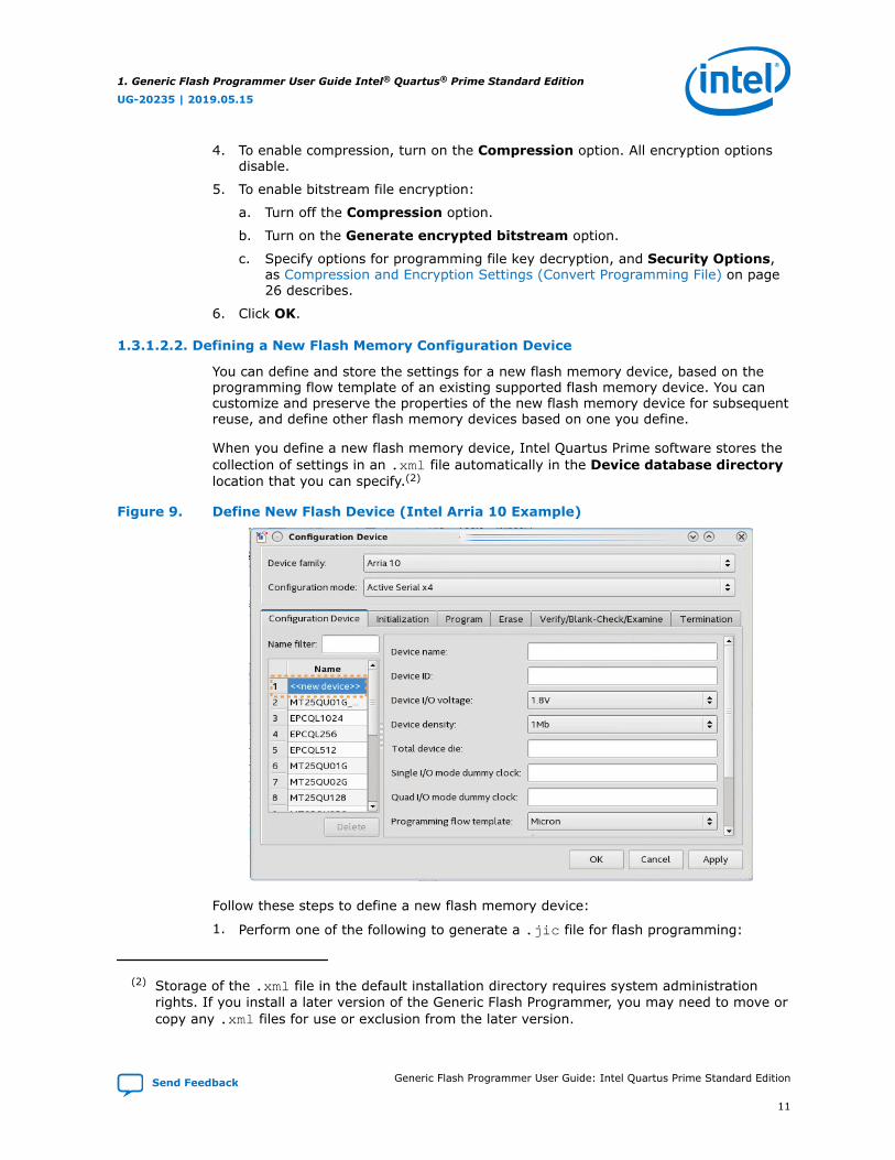
1.3.1.2.2. Defining a New Flash Memory Configuration Device
You can define and store the settings for a new flash memory device, based on theprogramming flow template of an existing supported flash memory device. You cancustomize and preserve the properties of the new flash memory device for subsequentreuse, and define other flash memory devices based on one you define.
When you define a new flash memory device, Intel Quartus Prime software stores thecollection of settings in an .xml file automatically in the Device database directorylocation that you can specify.(2)
Figure 9. Define New Flash Device (Intel Arria 10 Example)
Follow these steps to define a new flash memory device:
1. Perform one of the following to generate a .jic file for flash programming:
(2) Storage of the .xml file in the default installation directory requires system administrationrights. If you install a later version of the Generic Flash Programmer, you may need to move orcopy any .xml files for use or exclusion from the later version.
1. Generic Flash Programmer User Guide Intel® Quartus® Prime Standard Edition
UG-20235 | 2019.05.15
Send Feedback Generic Flash Programmer User Guide: Intel Quartus Prime Standard Edition
11
• Step 2: Generate Secondary Programming Files (Convert Programming Files)on page 7
2. For the Configuration Device option, select <<new device>>. The settings onthis and other tabs become available.
3. For Programming flow template, select an existing flash memory devicetemplate for the new device initial settings, or define a flash programming flow fora different flash memory vendor based on an existing template.
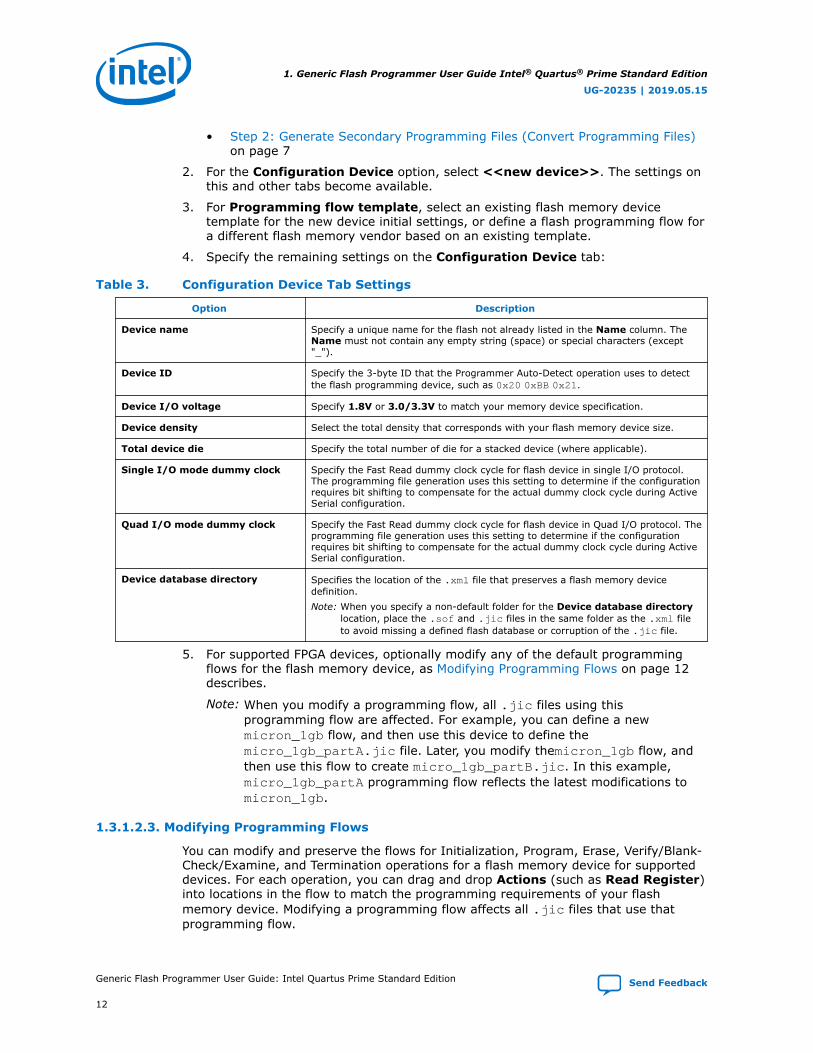
4. Specify the remaining settings on the Configuration Device tab:
Table 3. Configuration Device Tab Settings
Option Description
Device name Specify a unique name for the flash not already listed in the Name column. TheName must not contain any empty string (space) or special characters (except"_").
Device ID Specify the 3-byte ID that the Programmer Auto-Detect operation uses to detectthe flash programming device, such as 0x20 0xBB 0x21.
Device I/O voltage Specify 1.8V or 3.0/3.3V to match your memory device specification.
Device density Select the total density that corresponds with your flash memory device size.
Total device die Specify the total number of die for a stacked device (where applicable).
Single I/O mode dummy clock Specify the Fast Read dummy clock cycle for flash device in single I/O protocol.The programming file generation uses this setting to determine if the configurationrequires bit shifting to compensate for the actual dummy clock cycle during ActiveSerial configuration.
Quad I/O mode dummy clock Specify the Fast Read dummy clock cycle for flash device in Quad I/O protocol. Theprogramming file generation uses this setting to determine if the configurationrequires bit shifting to compensate for the actual dummy clock cycle during ActiveSerial configuration.
Device database directory Specifies the location of the .xml file that preserves a flash memory devicedefinition.Note: When you specify a non-default folder for the Device database directory
location, place the .sof and .jic files in the same folder as the .xml fileto avoid missing a defined flash database or corruption of the .jic file.
5. For supported FPGA devices, optionally modify any of the default programmingflows for the flash memory device, as Modifying Programming Flows on page 12describes.
Note: When you modify a programming flow, all .jic files using thisprogramming flow are affected. For example, you can define a newmicron_1gb flow, and then use this device to define themicro_1gb_partA.jic file. Later, you modify themicron_1gb flow, andthen use this flow to create micro_1gb_partB.jic. In this example,micro_1gb_partA programming flow reflects the latest modifications tomicron_1gb.
1.3.1.2.3. Modifying Programming Flows
You can modify and preserve the flows for Initialization, Program, Erase, Verify/Blank-Check/Examine, and Termination operations for a flash memory device for supporteddevices. For each operation, you can drag and drop Actions (such as Read Register)into locations in the flow to match the programming requirements of your flashmemory device. Modifying a programming flow affects all .jic files that use thatprogramming flow.
1. Generic Flash Programmer User Guide Intel® Quartus® Prime Standard Edition
UG-20235 | 2019.05.15
Generic Flash Programmer User Guide: Intel Quartus Prime Standard Edition Send Feedback
12
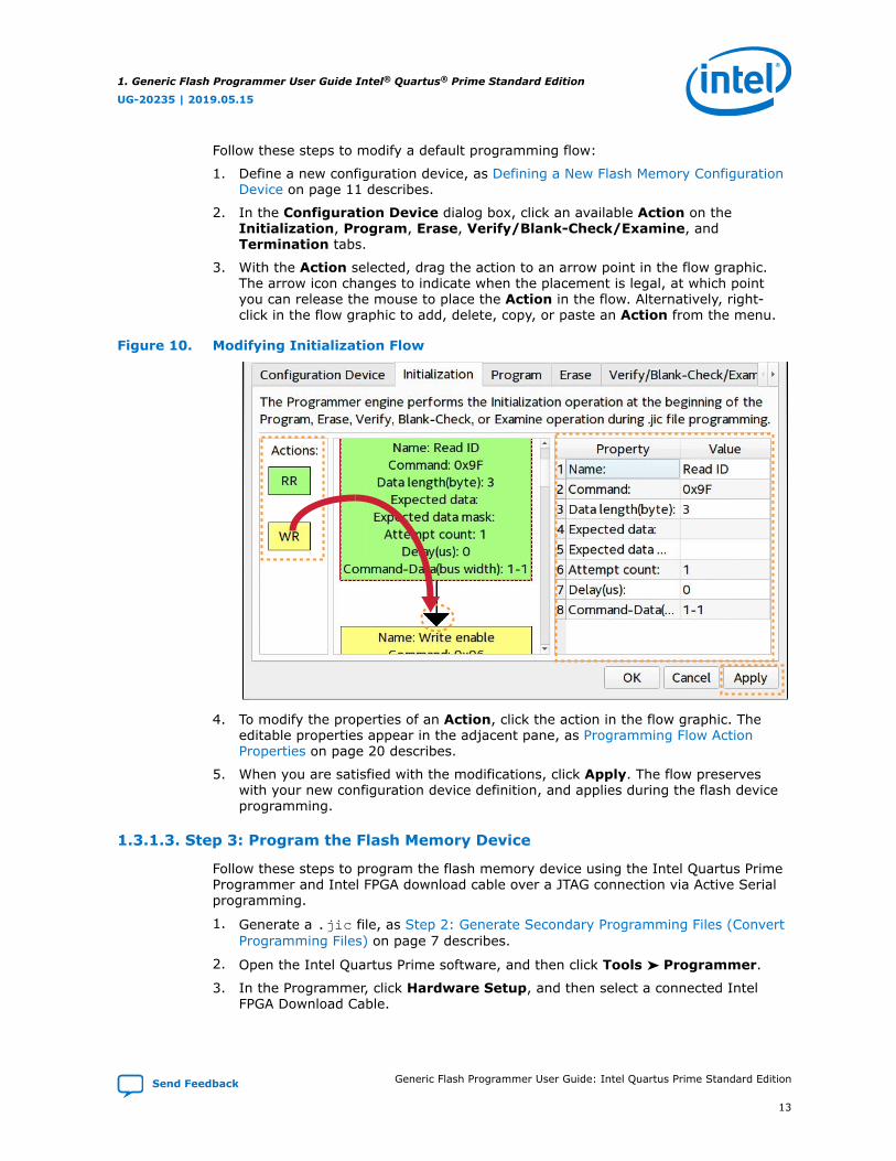
Follow these steps to modify a default programming flow:
1. Define a new configuration device, as Defining a New Flash Memory ConfigurationDevice on page 11 describes.
2. In the Configuration Device dialog box, click an available Action on theInitialization, Program, Erase, Verify/Blank-Check/Examine, andTermination tabs.
3. With the Action selected, drag the action to an arrow point in the flow graphic.The arrow icon changes to indicate when the placement is legal, at which pointyou can release the mouse to place the Action in the flow. Alternatively, right-click in the flow graphic to add, delete, copy, or paste an Action from the menu.
Figure 10. Modifying Initialization Flow
4. To modify the properties of an Action, click the action in the flow graphic. Theeditable properties appear in the adjacent pane, as Programming Flow ActionProperties on page 20 describes.
5. When you are satisfied with the modifications, click Apply. The flow preserveswith your new configuration device definition, and applies during the flash deviceprogramming.
1.3.1.3. Step 3: Program the Flash Memory Device
Follow these steps to program the flash memory device using the Intel Quartus PrimeProgrammer and Intel FPGA download cable over a JTAG connection via Active Serialprogramming.
1. Generate a .jic file, as Step 2: Generate Secondary Programming Files (ConvertProgramming Files) on page 7 describes.
2. Open the Intel Quartus Prime software, and then click Tools ➤ Programmer.
3. In the Programmer, click Hardware Setup, and then select a connected IntelFPGA Download Cable.
1. Generic Flash Programmer User Guide Intel® Quartus® Prime Standard Edition
UG-20235 | 2019.05.15
Send Feedback Generic Flash Programmer User Guide: Intel Quartus Prime Standard Edition
13
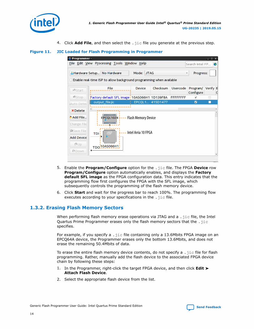
4. Click Add File, and then select the .jic file you generate at the previous step.
Figure 11. JIC Loaded for Flash Programming in Programmer
Flash Memory Device
Intel Arria 10 FPGA
5. Enable the Program/Configure option for the .jic file. The FPGA Device rowProgram/Configure option automatically enables, and displays the Factorydefault SFL image as the FPGA configuration data. This entry indicates that theprogramming flow first configures the FPGA with the SFL image, whichsubsequently controls the programming of the flash memory device.
6. Click Start and wait for the progress bar to reach 100%. The programming flowexecutes according to your specifications in the .jic file.
1.3.2. Erasing Flash Memory Sectors
When performing flash memory erase operations via JTAG and a .jic file, the IntelQuartus Prime Programmer erases only the flash memory sectors that the .jicspecifies.
For example, if you specify a .jic file containing only a 13.6Mbits FPGA image on anEPCQ64A device, the Programmer erases only the bottom 13.6Mbits, and does noterase the remaining 50.4Mbits of data.
To erase the entire flash memory device contents, do not specify a .jic file for flashprogramming. Rather, manually add the flash device to the associated FPGA devicechain by following these steps:
1. In the Programmer, right-click the target FPGA device, and then click Edit ➤Attach Flash Device.
2. Select the appropriate flash device from the list.
1. Generic Flash Programmer User Guide Intel® Quartus® Prime Standard Edition
UG-20235 | 2019.05.15
Generic Flash Programmer User Guide: Intel Quartus Prime Standard Edition Send Feedback
14
1.4. Generic Flash Programmer Flow Templates (ConvertProgramming File)
For supported devices, you can modify and preserve the default programming flows,as Modifying Programming Flows on page 12 describes.
The following describe the templates for each programming flow:
Related Information
• Initialization Flow Templates (Convert Programming File) on page 15
• Program Flow Template (Convert Programming File) on page 16
• Erase Flow Template (Convert Programming File) on page 17
• Verify/Blank-Check/Examine Flow Template (Convert Programming File) on page18
• Termination Flow Template (Convert Programming File) on page 19
• Programming Flow Action Properties on page 20
1.4.1. Initialization Flow Templates (Convert Programming File)
The Initialization flow template has the following Actions.
1. Generic Flash Programmer User Guide Intel® Quartus® Prime Standard Edition
UG-20235 | 2019.05.15
Send Feedback Generic Flash Programmer User Guide: Intel Quartus Prime Standard Edition
15
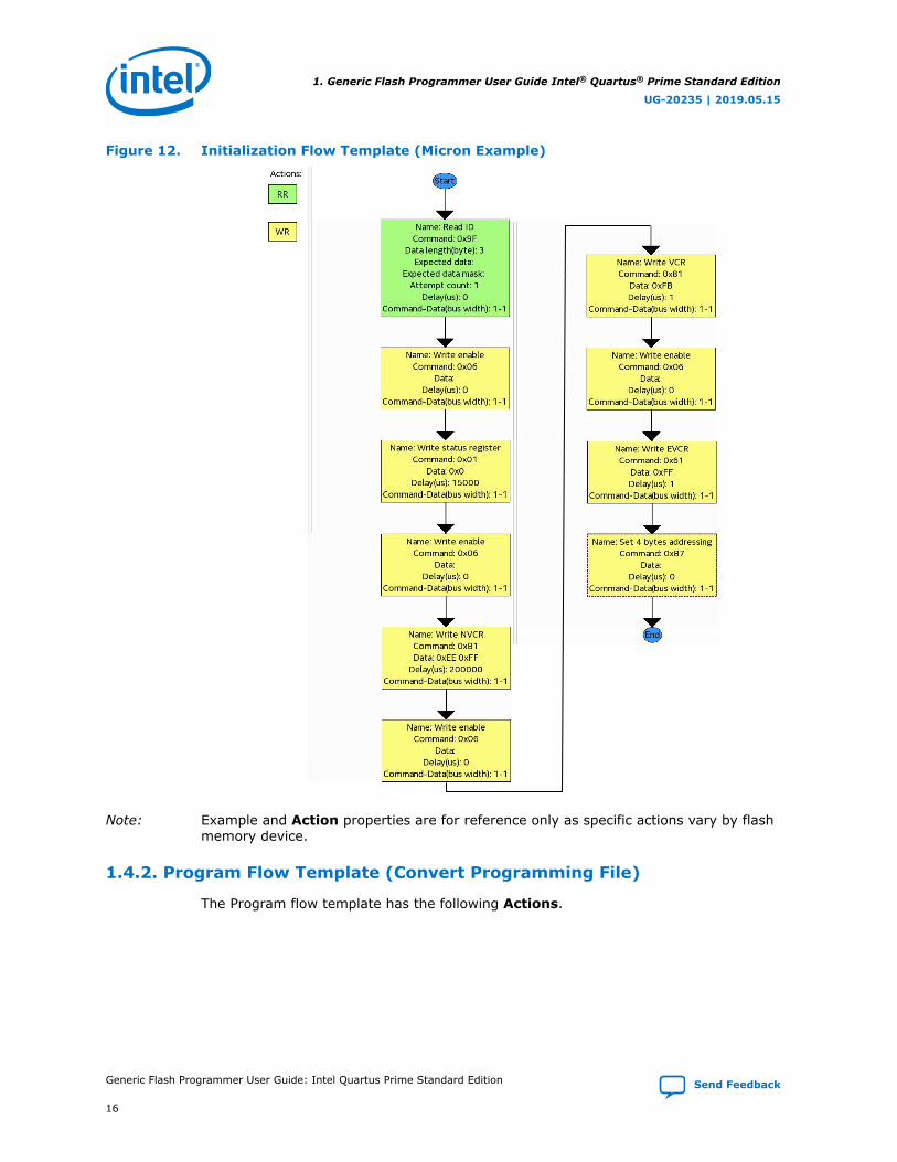
Figure 12. Initialization Flow Template (Micron Example)
Note: Example and Action properties are for reference only as specific actions vary by flashmemory device.
1.4.2. Program Flow Template (Convert Programming File)
The Program flow template has the following Actions.
1. Generic Flash Programmer User Guide Intel® Quartus® Prime Standard Edition
UG-20235 | 2019.05.15
Generic Flash Programmer User Guide: Intel Quartus Prime Standard Edition Send Feedback
16
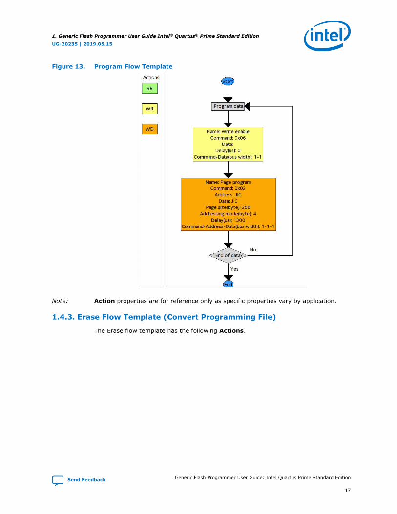
Figure 13. Program Flow Template
Note: Action properties are for reference only as specific properties vary by application.
1.4.3. Erase Flow Template (Convert Programming File)
The Erase flow template has the following Actions.
1. Generic Flash Programmer User Guide Intel® Quartus® Prime Standard Edition
UG-20235 | 2019.05.15
Send Feedback Generic Flash Programmer User Guide: Intel Quartus Prime Standard Edition
17
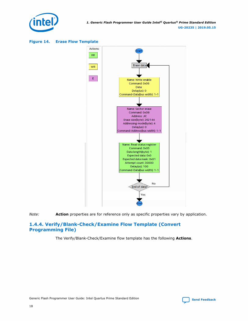
Figure 14. Erase Flow Template
Note: Action properties are for reference only as specific properties vary by application.
1.4.4. Verify/Blank-Check/Examine Flow Template (ConvertProgramming File)
The Verify/Blank-Check/Examine flow template has the following Actions.
1. Generic Flash Programmer User Guide Intel® Quartus® Prime Standard Edition
UG-20235 | 2019.05.15
Generic Flash Programmer User Guide: Intel Quartus Prime Standard Edition Send Feedback
18
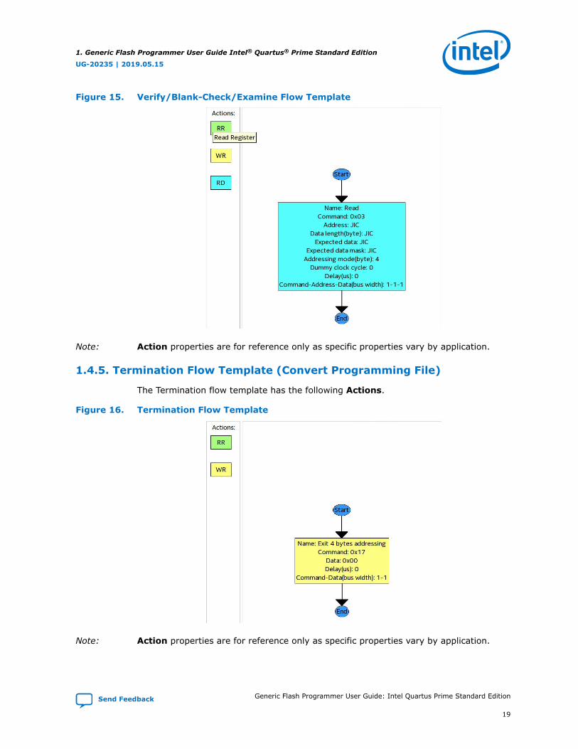
Figure 15. Verify/Blank-Check/Examine Flow Template
Note: Action properties are for reference only as specific properties vary by application.
1.4.5. Termination Flow Template (Convert Programming File)
The Termination flow template has the following Actions.
Figure 16. Termination Flow Template
Note: Action properties are for reference only as specific properties vary by application.
1. Generic Flash Programmer User Guide Intel® Quartus® Prime Standard Edition
UG-20235 | 2019.05.15
Send Feedback Generic Flash Programmer User Guide: Intel Quartus Prime Standard Edition
19
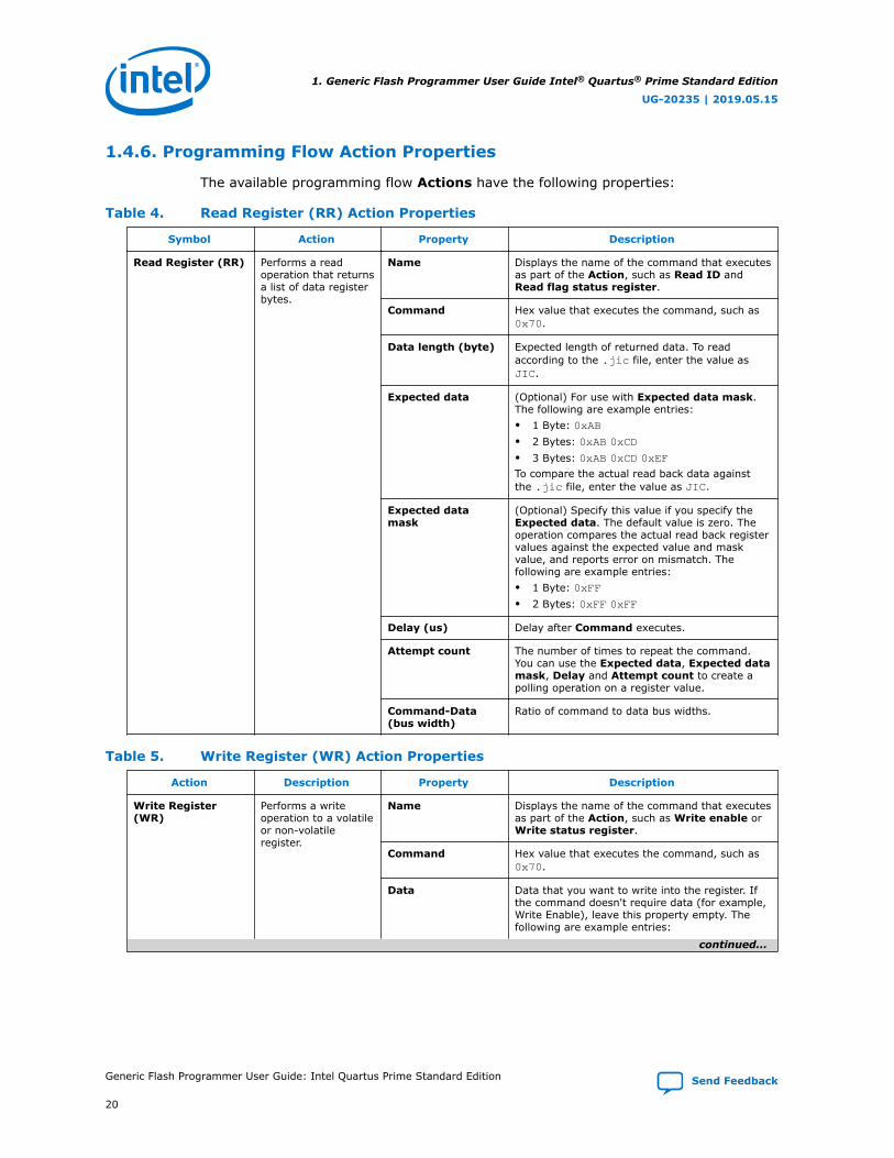
1.4.6. Programming Flow Action Properties
The available programming flow Actions have the following properties:
Table 4. Read Register (RR) Action Properties
Symbol Action Property Description
Read Register (RR) Performs a readoperation that returnsa list of data registerbytes.
Name Displays the name of the command that executesas part of the Action, such as Read ID andRead flag status register.
Command Hex value that executes the command, such as0x70.
Data length (byte) Expected length of returned data. To readaccording to the .jic file, enter the value asJIC.
Expected data (Optional) For use with Expected data mask.The following are example entries:• 1 Byte: 0xAB• 2 Bytes: 0xAB 0xCD• 3 Bytes: 0xAB 0xCD 0xEFTo compare the actual read back data againstthe .jic file, enter the value as JIC.
Expected datamask
(Optional) Specify this value if you specify theExpected data. The default value is zero. Theoperation compares the actual read back registervalues against the expected value and maskvalue, and reports error on mismatch. Thefollowing are example entries:• 1 Byte: 0xFF• 2 Bytes: 0xFF 0xFF
Delay (us) Delay after Command executes.
Attempt count The number of times to repeat the command.You can use the Expected data, Expected datamask, Delay and Attempt count to create apolling operation on a register value.
Command-Data(bus width)
Ratio of command to data bus widths.
Table 5. Write Register (WR) Action Properties
Action Description Property Description
Write Register(WR)
Performs a writeoperation to a volatileor non-volatileregister.
Name Displays the name of the command that executesas part of the Action, such as Write enable orWrite status register.
Command Hex value that executes the command, such as0x70.
Data Data that you want to write into the register. Ifthe command doesn't require data (for example,Write Enable), leave this property empty. Thefollowing are example entries:
continued...
1. Generic Flash Programmer User Guide Intel® Quartus® Prime Standard Edition
UG-20235 | 2019.05.15
Generic Flash Programmer User Guide: Intel Quartus Prime Standard Edition Send Feedback
20
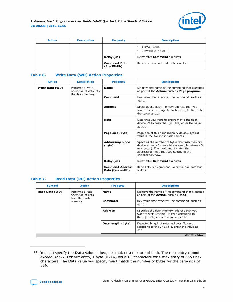
Action Description Property Description
• 1 Byte: 0xAB• 2 Bytes: 0xAB 0xCD
Delay (us) Delay after Command executes.
Command-Data(Bus Width)
Ratio of command to data bus widths.
Table 6. Write Data (WD) Action Properties
Action Description Property Description
Write Data (WD) Performs a writeoperation of data intothe flash memory.
Name Displays the name of the command that executesas part of the Action, such as Page program.
Command Hex value that executes the command, such as0x70.
Address Specifies the flash memory address that youwant to start writing. To flash the .jic file, enterthe value as JIC.
Data Data that you want to program into the flashdevice.(3) To flash the .jic file, enter the valueas JIC.
Page size (byte) Page size of this flash memory device. Typicalvalue is 256 for most flash devices.
Addressing mode(byte)
Specifies the number of bytes the flash memorydevice expects for an address (switch between 3or 4 bytes). The mode must match theaddressing mode that you specify in theInitialization flow.
Delay (us) Delay after Command executes.
Command-Address-Data (bus width)
Ratio between command, address, and data buswidths.
Table 7. Read Data (RD) Action Properties
Symbol Action Property Description
Read Data (WD) Performs a readoperation of datafrom the flashmemory.
Name Displays the name of the command that executesas part of the Action, such as Read.
Command Hex value that executes the command, such as0x70.
Address Specifies the flash memory address that youwant to start reading. To read according tothe .jic file, enter the value as JIC.
Data length (byte) Expected length of returned data. To readaccording to the .jic file, enter the value asJIC.
continued...
(3) You can specify the Data value in hex, decimal, or a mixture of both. The max entry cannotexceed 32727. For hex entry, 1 byte (0xAA) equals 5 characters for a max entry of 6553 hexcharacters. The Data value you specify must match the number of bytes for the page size of256.
1. Generic Flash Programmer User Guide Intel® Quartus® Prime Standard Edition
UG-20235 | 2019.05.15
Send Feedback Generic Flash Programmer User Guide: Intel Quartus Prime Standard Edition
21
Symbol Action Property Description
Expected data (Optional) For use with Expected data mask.The following are example entries:• 1 Byte: 0xAB• 2 Bytes: 0xAB 0xCD• 3 Bytes: 0xAB 0xCD 0xEFTo compare the actual read back data againstthe .jic file, enter the value as JIC.
Expected data mask If you specify the Expected data mask, thenthe operation compares the actual read back dataagainst the expected value and mask value, andreports an error on mismatch. If you want tocompare against the .jic file, enter the value asJIC.
Addressing mode(byte)
Specifies the number of bytes the flash memorydevice expects for an address (switch between 3or 4 bytes). The mode must match theaddressing mode that you specify in theInitialization flow.
Dummy clock cycle Specifies the number of dummy clock cyclessubsequent to the Command.
Delay (us) Delay after Command executes.
Command-Address-Data (bus width)
Ratio between command, address, and data buswidths.
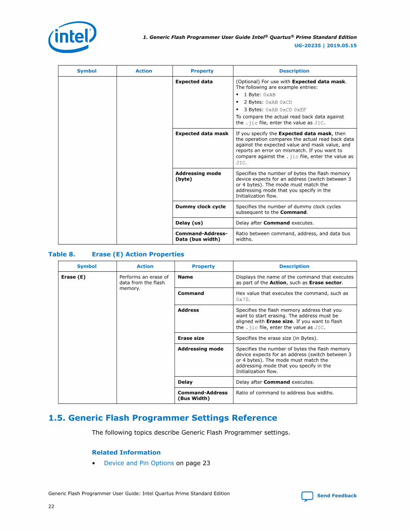
Table 8. Erase (E) Action Properties
Symbol Action Property Description
Erase (E) Performs an erase ofdata from the flashmemory.
Name Displays the name of the command that executesas part of the Action, such as Erase sector.
Command Hex value that executes the command, such as0x70.
Address Specifies the flash memory address that youwant to start erasing. The address must bealigned with Erase size. If you want to flashthe .jic file, enter the value as JIC.
Erase size Specifies the erase size (in Bytes).
Addressing mode Specifies the number of bytes the flash memorydevice expects for an address (switch between 3or 4 bytes). The mode must match theaddressing mode that you specify in theInitialization flow.
Delay Delay after Command executes.
Command-Address(Bus Width)
Ratio of command to address bus widths.
1.5. Generic Flash Programmer Settings Reference
The following topics describe Generic Flash Programmer settings.
Related Information
• Device and Pin Options on page 23
1. Generic Flash Programmer User Guide Intel® Quartus® Prime Standard Edition
UG-20235 | 2019.05.15
Generic Flash Programmer User Guide: Intel Quartus Prime Standard Edition Send Feedback
22

• SOF Data Properties Dialog Box (Convert Programming File) on page 27
• Compression and Encryption Settings (Convert Programming File) on page 26
• Convert Programming File Dialog Box on page 23
1.5.1. Convert Programming File Dialog Box
Allows you to convert or combine one or more secondary programming files thatsupport alternative device configuration schemes, such as flash programming, partialreconfiguration, or remote system update.
Table 9. Convert Programming File Dialog Box Settings
Setting Description
Programming file type Allows you to specify a secondary programming file format for conversion of aprimary programming file. The Generic Flash Programmer supports only the .jicfile type.
Configuration device Allows you to select a predefined or define a new configuration device. Click the(…) button to define a new device and programming flow.
Mode Allows you to select the method of device configuration. The Generic FlashProgrammer supports only the Active Serial or Active Serial x4 modes.
Output file Specifies the location of the files that Convert Programming File generates. Bydefault this location is the top-level project directory.
Input files to convert Specifies one or more primary programming files for conversion or combinationinto one or more secondary programming files for alternative programmingmethods.
1.5.2. Device and Pin Options
The following tables describe Device & Pin Option settings that impact Generic FlashProgrammer. To access, click Assignments ➤ Device ➤ Device & Pin Options.
General Device Options
Allow you to specify basic device configuration options that are independent of aspecific configuration scheme. To access these settings, click Assignments ➤ Device➤ Device and Pin Options ➤ General.
Table 10. General Device Options
Option Description
Options • Auto-restart configuration after error—restarts the configuration processautomatically if a data error is encountered. If this option is turned off, youmust externally direct the device to restart the configuration process if an erroroccurs. This option is available for passive serial and active serial configurationschemes.
• Release clears before tri-states—releases the clear signal on registeredlogic cells and I/O cells before releasing the output enable override on tri-statebuffers. If this option is turned off, the output enable signals are releasedbefore the clear overrides are released.
• Enable user-supplied start-up clock (CLKUSR)—uses a user-supplied clockon the CLKUSR pin for initialization. When turned off, external circuitry isrequired to provide the initialization clock on the DCLK pin in the Passive Serialand Passive Parallel Synchronous configuration schemes; in the Passive ParallelAsynchronous configuration scheme, the device uses an internal initializationclock.
continued...
1. Generic Flash Programmer User Guide Intel® Quartus® Prime Standard Edition
UG-20235 | 2019.05.15
Send Feedback Generic Flash Programmer User Guide: Intel Quartus Prime Standard Edition
23
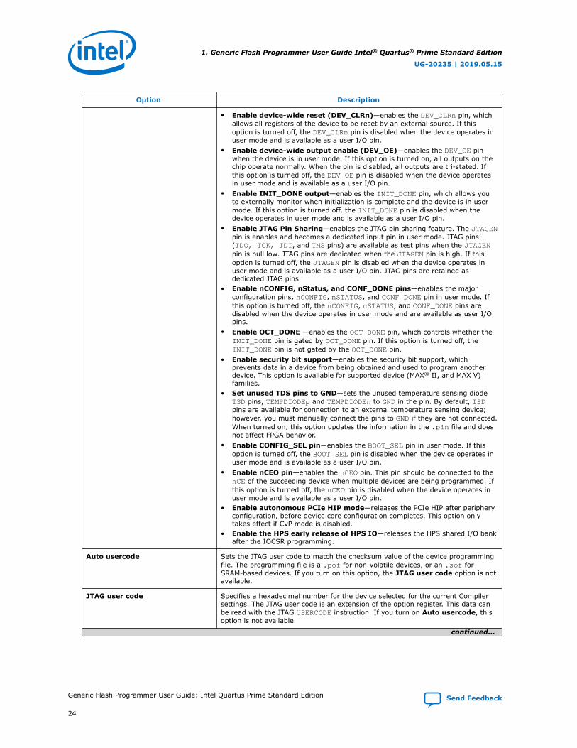
Option Description
• Enable device-wide reset (DEV_CLRn)—enables the DEV_CLRn pin, whichallows all registers of the device to be reset by an external source. If thisoption is turned off, the DEV_CLRn pin is disabled when the device operates inuser mode and is available as a user I/O pin.
• Enable device-wide output enable (DEV_OE)—enables the DEV_OE pinwhen the device is in user mode. If this option is turned on, all outputs on thechip operate normally. When the pin is disabled, all outputs are tri-stated. Ifthis option is turned off, the DEV_OE pin is disabled when the device operatesin user mode and is available as a user I/O pin.
• Enable INIT_DONE output—enables the INIT_DONE pin, which allows youto externally monitor when initialization is complete and the device is in usermode. If this option is turned off, the INIT_DONE pin is disabled when thedevice operates in user mode and is available as a user I/O pin.
• Enable JTAG Pin Sharing—enables the JTAG pin sharing feature. The JTAGENpin is enables and becomes a dedicated input pin in user mode. JTAG pins(TDO, TCK, TDI, and TMS pins) are available as test pins when the JTAGENpin is pull low. JTAG pins are dedicated when the JTAGEN pin is high. If thisoption is turned off, the JTAGEN pin is disabled when the device operates inuser mode and is available as a user I/O pin. JTAG pins are retained asdedicated JTAG pins.
• Enable nCONFIG, nStatus, and CONF_DONE pins—enables the majorconfiguration pins, nCONFIG, nSTATUS, and CONF_DONE pin in user mode. Ifthis option is turned off, the nCONFIG, nSTATUS, and CONF_DONE pins aredisabled when the device operates in user mode and are available as user I/Opins.
• Enable OCT_DONE —enables the OCT_DONE pin, which controls whether theINIT_DONE pin is gated by OCT_DONE pin. If this option is turned off, theINIT_DONE pin is not gated by the OCT_DONE pin.
• Enable security bit support—enables the security bit support, whichprevents data in a device from being obtained and used to program anotherdevice. This option is available for supported device (MAX® II, and MAX V)families.
• Set unused TDS pins to GND—sets the unused temperature sensing diodeTSD pins, TEMPDIODEp and TEMPDIODEn to GND in the pin. By default, TSDpins are available for connection to an external temperature sensing device;however, you must manually connect the pins to GND if they are not connected.When turned on, this option updates the information in the .pin file and doesnot affect FPGA behavior.
• Enable CONFIG_SEL pin—enables the BOOT_SEL pin in user mode. If thisoption is turned off, the BOOT_SEL pin is disabled when the device operates inuser mode and is available as a user I/O pin.
• Enable nCEO pin—enables the nCEO pin. This pin should be connected to thenCE of the succeeding device when multiple devices are being programmed. Ifthis option is turned off, the nCEO pin is disabled when the device operates inuser mode and is available as a user I/O pin.
• Enable autonomous PCIe HIP mode—releases the PCIe HIP after peripheryconfiguration, before device core configuration completes. This option onlytakes effect if CvP mode is disabled.
• Enable the HPS early release of HPS IO—releases the HPS shared I/O bankafter the IOCSR programming.
Auto usercode Sets the JTAG user code to match the checksum value of the device programmingfile. The programming file is a .pof for non-volatile devices, or an .sof forSRAM-based devices. If you turn on this option, the JTAG user code option is notavailable.
JTAG user code Specifies a hexadecimal number for the device selected for the current Compilersettings. The JTAG user code is an extension of the option register. This data canbe read with the JTAG USERCODE instruction. If you turn on Auto usercode, thisoption is not available.
continued...
1. Generic Flash Programmer User Guide Intel® Quartus® Prime Standard Edition
UG-20235 | 2019.05.15
Generic Flash Programmer User Guide: Intel Quartus Prime Standard Edition Send Feedback
24
Option Description
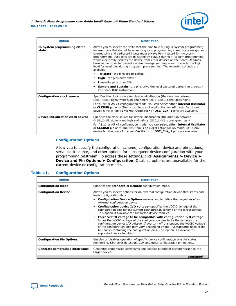
In-system programming clampstate
Allows you to specify the state that the pins take during in-system programmingfor used pins that do not have an in-system programming clamp state assignment.Unused pins and dedicated inputs must always be tri-stated for in-systemprogramming. Used pins are tri-stated by default during in-system programming,which electrically isolates the device from other devices on the board. At times,however, in order to prevent system damage you may want to specify the logiclevel for used pins during in-system programming. The following settings areavailable:• Tri-state—the pins are tri-stated.• High—the pins drive VCCIO.• Low—the pins drive GND.• Sample and Sustain—the pins drive the level captured during the SAMPLE/
PRELOAD JTAG instruction.
Configuration clock source Specifies the clock source for device initialization (the duration betweenCONF_DONE signal went high and before INIT_DONE signal goes high).For AS x1 or AS x4 configuration mode, you can select either Internal Oscillatoror CLKUSR pin only. The DCLK pin is an illegal option for AS mode. In 14 nmdevice families, only Internal Oscillator or OSC_CLK_1 pins are available.
Device initialization clock source Specifies the clock source for device initialization (the duration betweenCONF_DONE signal went high and before INIT_DONE signal goes high).For AS x1 or AS x4 configuration mode, you can select either Internal Oscillatoror CLKUSR pin only. The DCLK pin is an illegal option for AS mode. In 14 nmdevice families, only Internal Oscillator or OSC_CLK_1 pins are available.
Configuration Options
Allow you to specify the configuration scheme, configuration device and pin options,serial clock source, and other options for subsequent device configuration with yourprogramming bitstream. To access these settings, click Assignments ➤ Device ➤Device and Pin Options ➤ Configuration. Disabled options are unavailable for thecurrent device or configuration mode.
Table 11. Configuration Options
Option Description
Configuration mode Specifies the Standard or Remote configuration mode.
Configuration Device Allows you to specify options for an external configuration device that stores andloads configuration data.• Configuration Device Options—allows you to define the properties of an
external configuration device.• Configuration device I/O voltage—specifies the VCCIO voltage of the
configuration pins for the current configuration scheme of the target device.This option is available for supported device families.
• Force VCCIO voltage to be compatible with configuration I/O voltage—forces the VCCIO voltage of the configuration pins to be the same as theconfiguration device I/O voltage. If you turn off this option, the VCCIO voltageof the configuration pins may vary depending on the I/O standards used in theI/O banks containing the configuration pins. This option is available forsupported device families.
Configuration Pin Options Enables or disables operation of specific device configuration pins for statusmonitoring, SEU error detection, CvP, and other configuration pin options.
Generate compressed bitstreams Generates compressed bitstreams and enables bitstream decompression in thetarget device.
continued...
1. Generic Flash Programmer User Guide Intel® Quartus® Prime Standard Edition
UG-20235 | 2019.05.15
Send Feedback Generic Flash Programmer User Guide: Intel Quartus Prime Standard Edition
25
Option Description
Active serial clock source Specifies the configuration clock source for Active Serial programming. Optionsrange from 12.5 MHz to 100 MHz.
VID Operation Mode Enables Voltage IDentification logic in the target device with selected operationmode. The available options are PMBus Master or PMBus Slave.
Disable Register Power-UpInitialization
Tri-states the Active Configuration pins in user mode. The Compiler ignores thissetting if the configuration scheme you select is not an Active Configurationscheme.
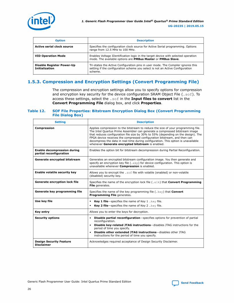
1.5.3. Compression and Encryption Settings (Convert Programming File)
The compression and encryption settings allow you to specify options for compressionand encryption key security for the device configuration SRAM Object File (.sof). Toaccess these settings, select the .sof in the Input files to convert list in theConvert Programming File dialog box, and click Properties.
Table 12. SOF File Properties: Bitstream Encryption Dialog Box (Convert ProgrammingFile Dialog Box)
Setting Description
Compression Applies compression to the bitstream to reduce the size of your programming file.The Intel Quartus Prime Assembler can generate a compressed bitstream imagethat reduces configuration file size by 30% to 55% (depending on the design). TheFPGA device receives the compressed configuration bitstream, and then candecompress the data in real-time during configuration. This option is unavailablewhenever Generate encrypted bitstream is enabled.
Enable decompression duringpartial reconfiguration
Enables the option bit for bitstream decompression during Partial Reconfiguration.
Generate encrypted bitstream Generates an encrypted bitstream configuration image. You then generate andspecify an encryption key file (.ekp) for device configuration. This option isunavailable whenever Compression is enabled.
Enable volatile security key Allows you to encrypt the .sof file with volatile (enabled) or non-volatile(disabled) security key.
Generate encryption lock file Specifies the name of the encryption lock file (.elk) that Convert ProgrammingFile generates.
Generate key programming file Specifies the name of the key programming file (.key) that ConvertProgramming File generates.
Use key file • Key 1 file—specifies the name of Key 1 .key file.• Key 2 file—specifies the name of Key 2 .key file.
Key entry Allows you to enter the keys for decryption.
Security options • Disable partial reconfiguration—specifies options for prevention of partialreconfiguration.
• Disable key-related JTAG instructions—disables JTAG instructions for theperiod of time you specify.
• Disable other extended JTAG instructions—disables other JTAGinstructions for the period of time you specify.
Design Security FeatureDisclaimer
Acknowledges required acceptance of Design Security Disclaimer.
1. Generic Flash Programmer User Guide Intel® Quartus® Prime Standard Edition
UG-20235 | 2019.05.15
Generic Flash Programmer User Guide: Intel Quartus Prime Standard Edition Send Feedback
26
1.5.4. SOF Data Properties Dialog Box (Convert Programming File)
Allows you to define flash memory pages that store configuration data. To access fromthe Convert Programming File dialog box, click the SOF Data item and click theProperties button.
The following settings are available:
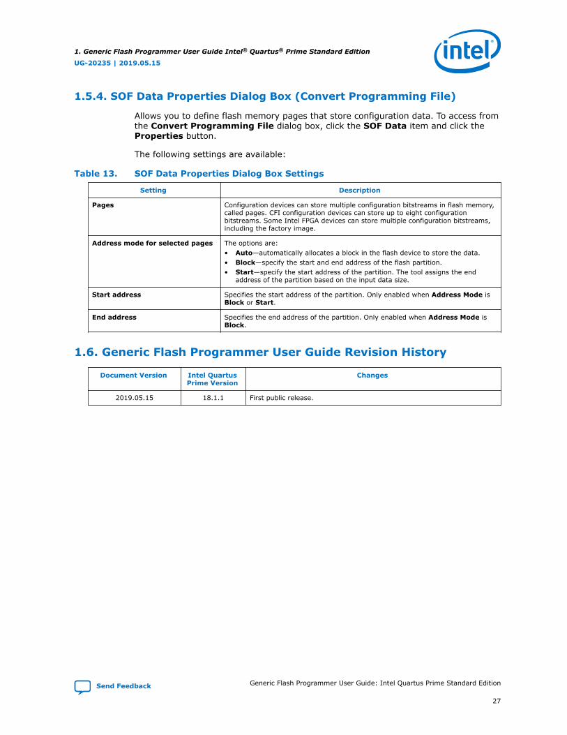
Table 13. SOF Data Properties Dialog Box Settings
Setting Description
Pages Configuration devices can store multiple configuration bitstreams in flash memory,called pages. CFI configuration devices can store up to eight configurationbitstreams. Some Intel FPGA devices can store multiple configuration bitstreams,including the factory image.
Address mode for selected pages The options are:• Auto—automatically allocates a block in the flash device to store the data.• Block—specify the start and end address of the flash partition.• Start—specify the start address of the partition. The tool assigns the end
address of the partition based on the input data size.
Start address Specifies the start address of the partition. Only enabled when Address Mode isBlock or Start.
End address Specifies the end address of the partition. Only enabled when Address Mode isBlock.
1.6. Generic Flash Programmer User Guide Revision History
Document Version Intel QuartusPrime Version
Changes
2019.05.15 18.1.1 First public release.
1. Generic Flash Programmer User Guide Intel® Quartus® Prime Standard Edition
UG-20235 | 2019.05.15
Send Feedback Generic Flash Programmer User Guide: Intel Quartus Prime Standard Edition
27