Embed Size (px)
Citation preview
Genetic algorithm based PI controller forDC-DC converter applied to Renewable
energy applications
D.Sivamani, 1 R. Harikrishnan, 2, R.Essakiraj 3
1PG Student M.E (PED) , Sathyabama University,Chennai-600119, India.
2Assistant Professor , Sathyabama University,Chennai-600119,India.
3Assistant Professor , Rajalakshmi Engineering College,Chennai-602105, India.
January 2, 2018
Abstract
This paper shows a system for tuning Genetic Algorithmbased PI(proportional Integral ) feedback controller for DC-DC converter (Buck -Boost Converter) which is applied toself excited Induction Generator used in WECS(Wind en-ergy conversion System). Due to non linear characteristicof the converter, a controller with better execution is re-quired. Pulse Width Modulation strategy is utilized forthe converter gating pulses. PI controller is choose becauselarge values tend to instabilities in the system response andto reduce steady state error. PI Controller is used for bettergain and accuracy. GENETIC ALGORITHM is an adap-tive method to solve search and optimization problems, Thecontroller parameters are optimized to produce reasonabletransient response without affecting the stable operation.Output voltage value of DC DC converter is either more im-portant or lesser than the input data voltage measured. Thevariable AC voltage from self excited Induction Generator is
1
International Journal of Pure and Applied MathematicsVolume 118 No. 16 2018, 1053-1071ISSN: 1311-8080 (printed version); ISSN: 1314-3395 (on-line version)url: http://www.ijpam.euSpecial Issue ijpam.eu
1053
converted into variable DC voltage and is connected to DCDC converter to get constant DC output voltage. Proposedmethodology is modeled by using MATLAB/SIMULINK re-sults are verified.
Key Words : DC-DC converter ; Pulse Width Modu-lation ; Duty cycle; PI controller; Genetic Algorithm.
1 INTRODUCTION
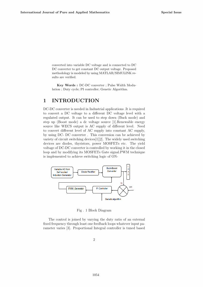
DC-DC converter is needed in Industrial applications .It is requiredto convert a DC voltage to a different DC voltage level with aregulated output. It can be used to step down (Buck mode) andstep up (Boost mode) a dc voltage source [1].Renewable energysource like WECS output is AC supply of different level. Needto convert different level of AC supply into constant AC supply,by using DC- DC converter . This conversion can be achieved byvariety of circuit switching devices[1][2]. The widely used switchingdevices are diodes, thyristors, power MOSFETs etc. The yieldvoltage of DC-DC converter is controlled by working it in the closedloop and by modifying its MOSFETs Gate signal.PWM techniqueis implemented to achieve switching logic of ON-
Fig . 1 Block Diagram
The control is joined by varying the duty ratio of an externalfixed frequency through least one feedback loops whatever input pa-rameter varies [3]. Proportional Integral controller is tuned based
2
International Journal of Pure and Applied Mathematics Special Issue
1054
on the Genetic Algorithm [4]. To enhance the transient response ofa framework by lessening (i) the peak overshoot , (ii) steady stateerror and (iii) shortening the settling time of the system[5]. GeneticAlgorithm is an optimization technique that performs a parallel,stochastic however immediate search to evaluate. The most com-mon method of Roulette wheel selection is implemented [6]. Theadvantages are GA searches a population focuses rather than singlesolution[7]. They are basicaly straight forward and robust but itcan be extended to wide variety of working conditions [8] .
The present paper proposes Genetic Algorithm based PI con-troller for Buck Boost converter. The feedback loop contains a PIcontroller which keeps the reference voltage and the output voltageof the plant as the error input and PWM technique used for oper-ating the gating signal. The Inductor in the plant stores the energyduring ON time [8]. The expressions are derived from switchedmodel of Buck Boost converter, small signal module of DC-DCconverter, feedback controller design. The performance is foundfrom WECS parameters, the recreated simulated Waveforms arepresented in the succeeding areas.
2 Buck Boost converter performance anal-
ysis
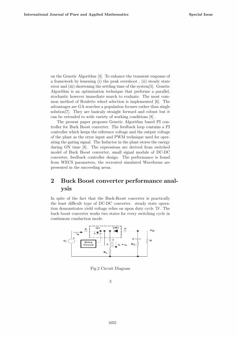
In spite of the fact that the Buck-Boost converter is practicallythe least difficult type of DC-DC converter. steady state opera-tion demonstrates yield voltage relies on upon duty cycle ’D’. Thebuck boost converter works two states for every switching cycle incontinuous conduction mode.
Fig.2 Circuit Diagram
3
International Journal of Pure and Applied Mathematics Special Issue
1055
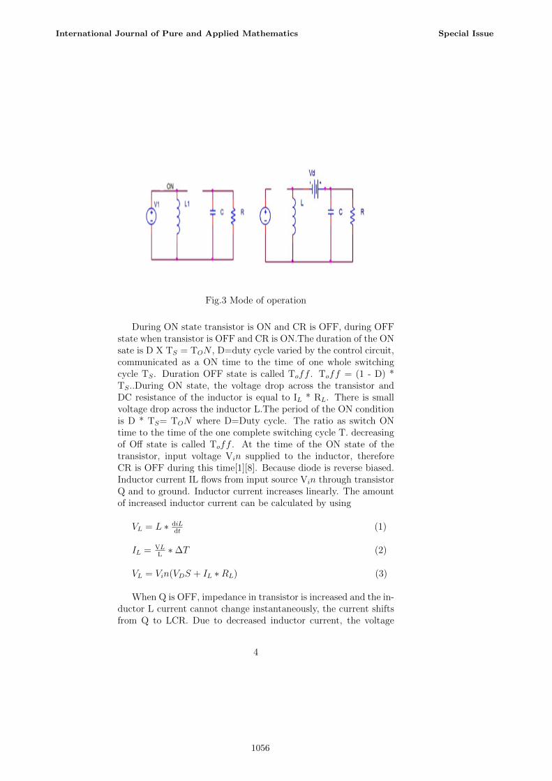
Fig.3 Mode of operation
During ON state transistor is ON and CR is OFF, during OFFstate when transistor is OFF and CR is ON.The duration of the ONsate is D X TS = TON , D=duty cycle varied by the control circuit,communicated as a ON time to the time of one whole switchingcycle TS. Duration OFF state is called Toff . Toff = (1 - D) *TS..During ON state, the voltage drop across the transistor andDC resistance of the inductor is equal to IL * RL. There is smallvoltage drop across the inductor L.The period of the ON conditionis D * TS= TON where D=Duty cycle. The ratio as switch ONtime to the time of the one complete switching cycle T. decreasingof Off state is called Toff . At the time of the ON state of thetransistor, input voltage Vin supplied to the inductor, thereforeCR is OFF during this time[1][8]. Because diode is reverse biased.Inductor current IL flows from input source Vin through transistorQ and to ground. Inductor current increases linearly. The amountof increased inductor current can be calculated by using
VL = L ∗ diLdt
(1)
IL = VLL
∗ ∆T (2)
VL = Vin(VDS + IL ∗RL) (3)
When Q is OFF, impedance in transistor is increased and the in-ductor L current cannot change instantaneously, the current shiftsfrom Q to LCR. Due to decreased inductor current, the voltage
4
International Journal of Pure and Applied Mathematics Special Issue
1056
across the inductor reverses its polarity until the rectifier CR be-comes forward biased. The inductor current IL flows from theoutput capacitor and load resistor combination through CR andground. Output voltage to be a negative voltage. Inductor currentdecreases during OFF time. During ON time of the transistor fromequation (3).
Ton = L∆IVs
(4)Energy stored in Inductor is
EL = 12L(V ston
L)2 (5)
During OFF time of transistor , Inductor current linearly de-creases from I2 to I1 .
Va = −Vs D1−D (6)
D ———> output conversion factor for buck converter(1- D ) ——> out put conversion factor for boost convertor
Input power = output power ,
Vs Is = Va * Ia , then Vs Is = Ia * Vs D/(1-D)
L = −Vs (1−D)∗V a∆I∗fs (7)
The average capacitor charging current during OFF time mustbe equal to the average capacitor discharging current during ONtime. The peak to peak ripple capacitor voltage Vc can be cal-culated by integrating the average capacitor discharging currentduring ON time[10]. Then the expression for capacitor value
C = D(Rfs)∗(Vco/Vo
(8)
Vo can be varied by varying the duty cycle D.The inductor provides current to the output only during OFF
state of the power period [7] . This average current over a entireswitching cycle is equal to the output current because the averagecurrent in the output capacitor should be equal to zero.
IL(Avg) = −Io(1−D)
(9)
5
International Journal of Pure and Applied Mathematics Special Issue
1057
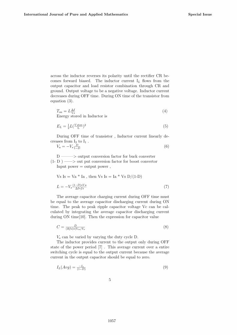
Fig.4 Duty cycle Vs Gain
Table ( i ) Variable input voltage,variable duty cycle,constant out-put voltage
The above table shows the variable input voltage , constant out-put voltage, variable ON timeOf transistor, Duty cycle of DC-DCConverter for Buck-Boost Converter. Buck mode D ¡0.5, Boostmode D¿0.5. . From Small signal Modeling of Buck-Boost Con-verter transfer function equations for both buck and boost modeare derived ,then the transfer function equations are given belowfor finding error signal[12].
6
International Journal of Pure and Applied Mathematics Special Issue
1058
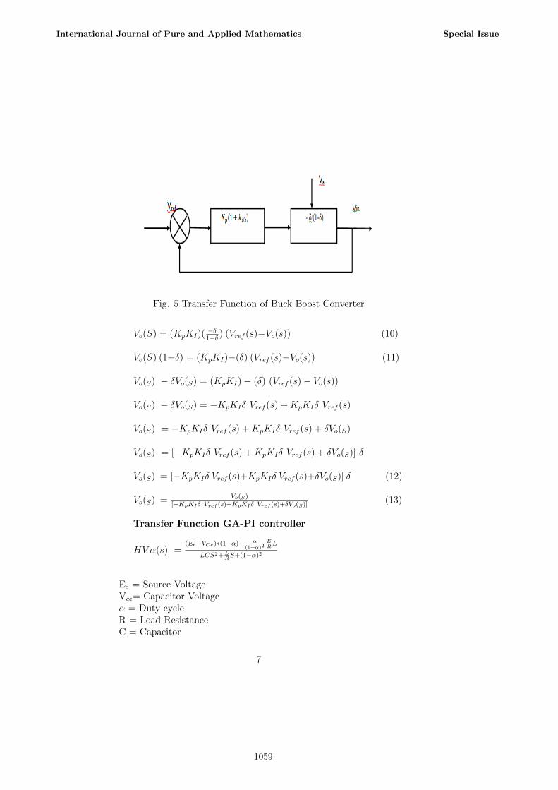
Fig. 5 Transfer Function of Buck Boost Converter
Vo(S) = (KpKI)(−δ1−δ ) (Vref (s)−Vo(s)) (10)
Vo(S) (1−δ) = (KpKI)−(δ) (Vref (s)−Vo(s)) (11)
Vo(S) − δVo(S) = (KpKI) − (δ) (Vref (s) − Vo(s))
Vo(S) − δVo(S) = −KpKIδ Vref (s) +KpKIδ Vref (s)
Vo(S) = −KpKIδ Vref (s) +KpKIδ Vref (s) + δVo(S)
Vo(S) = [−KpKIδ Vref (s) +KpKIδ Vref (s) + δVo(S)] δ
Vo(S) = [−KpKIδ Vref (s)+KpKIδ Vref (s)+δVo(S)] δ (12)
Vo(S) = Vo(S)[−KpKIδ Vref (s)+KpKIδ Vref (s)+δVo(S)]
(13)
Transfer Function GA-PI controller
HV α(s) =(Ee−VCe)∗(1−α)− α
(1+α)2ERL
LCS2+LRS+(1−α)2
Ee = Source VoltageVce= Capacitor Voltageα = Duty cycleR = Load ResistanceC = Capacitor
7
International Journal of Pure and Applied Mathematics Special Issue
1059
3 Structure of GA-Proportional Inte-
gral (PI) Controller
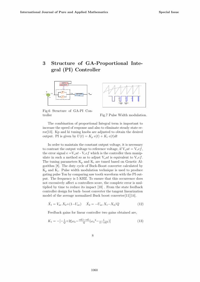
Fig.6 Structure of GA-PI Con-troller Fig.7 Pulse Width modulation.
The combination of proportional Integral term is important toincrease the speed of response and also to eliminate steady state er-ror[13]. Kp and ki tuning knobs are adjusted to obtain the desiredoutput. PI is given by U(t) = Kp e(t) +Ki e(t)dt
In order to maintain the constant output voltage, it is necessaryto contrast the output voltage to reference voltage, if Vout = Vref ,the error signal e =Vout - Vref which is the controller then manip-ulate in such a method so as to adjust Vout is equivalent to Vref .The tuning parameters Kp and Ki are tuned based on Genetic Al-gorithm [8]. The duty cycle of Buck-Boost converter calculated byKp and Ki. Pulse width modulation technique is used to producegating pulse Ton by comparing saw tooth waveform with the PI out-put. The frequency is 5 KHZ. To ensure that this occurrence doesnot excessively affect a controllers score, the complete error is mul-tiplied by time to reduce its impact [10] . From the state feedbackcontroller design for buck- boost converter the tangent linearizationmodel of the average normalized Buck boost converter[11][14].
X1 = Vav X2+(1−Uav) X2 = −Uav X1−X2/Q (12)
Feedback gains for linear controller two gains obtained are,
K1 = −[− 1Q
+2ξωn−vd(1−vd)Q
(ωn2− 1
(1−vd)2)] (13)
8
International Journal of Pure and Applied Mathematics Special Issue
1060
K2 = −[1−2VdQ
+(− 1Q
+2ξωn)−(1−Vd)(ωn2) 1(1−Vd)2
)] (14)
Where r = 1
(1−Vd)(1−Vd(1−2Vd)
Q)
(15)
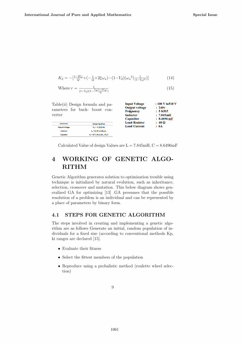
Table(ii) Design formula and pa-rameters for buck- boost con-verter
Calculated Value of design Values are L = 7.845mH, C = 8.6496mF
4 WORKING OF GENETIC ALGO-
RITHM
Genetic Algorithm generates solution to optimization trouble usingtechnique is initialized by natural evolution, such as inheritance,selection, crossover and mutation. This below diagram shows gen-eralized GA for optimizing [13] .GA presumes that the possibleresolution of a problem is an individual and can be represented bya place of parameters by binary form.
4.1 STEPS FOR GENETIC ALGORITHM
The steps involved in creating and implementing a genetic algo-rithm are as follows Generate an initial, random population of in-dividuals for a fixed size (according to conventional methods Kp,ki ranges are declared [15].
• Evaluate their fitness
• Select the fittest members of the population
• Reproduce using a probalistic method (roulette wheel selec-tion)
9
International Journal of Pure and Applied Mathematics Special Issue
1061
• Implement crossover operation on the reproduced chromo-somes
• Execute mutation operation with low probability
• Repeat step 2 until a predefined convergence criterion is met.
4.2 PSEUDO CODE AND FLOWCHART FORGENETIC ALGORITHM
Begin
t=0;Initialize P (t);calculate P (t);While ( not termination condition ) doBeginApply crossover and mutation to p(t) to yield c(t);Evaluate c (t);Select P(t+1) from P(t) and c(t);t= t+1;
End
End
The flowchart explains how genetic algorithms work is showingin the figure.11The process continuous till the best solution is foundout.
A scheme called roulette wheel selection is one of the most com-monly used techniques in such a proportionate selection mechanism.Selection procedure is listed above figure. The choice of Pm, Pc asthe control parameters can be a complex , nonlinear optimizationproblem[15].
10
International Journal of Pure and Applied Mathematics Special Issue
1062
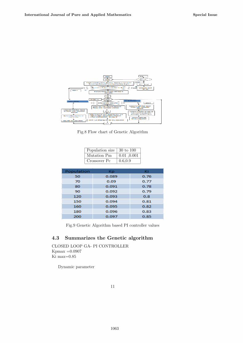
Fig.8 Flow chart of Genetic Algorithm
Population size 30 to 100Mutation Pm 0.01 ,0.001Crossover Pc 0.6,0.9
Fig.9 Genetic Algorithm based PI controller values
4.3 Summarizes the Genetic algorithm
CLOSED LOOP GA- PI CONTROLLERKpmax =0.0907Ki max=0.85
Dynamic parameter
11
International Journal of Pure and Applied Mathematics Special Issue
1063
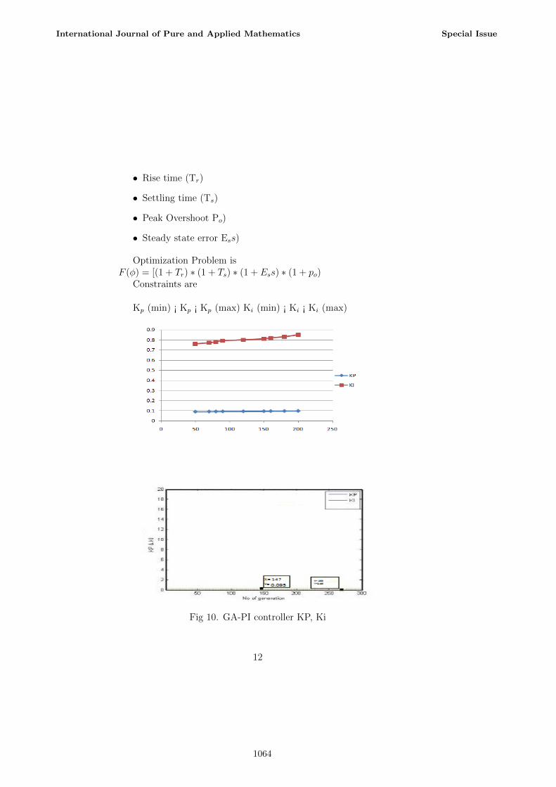
• Rise time (Tr)
• Settling time (Ts)
• Peak Overshoot Po)
• Steady state error Ess)
Optimization Problem isF (φ) = [(1 + Tr) ∗ (1 + Ts) ∗ (1 + Ess) ∗ (1 + po)
Constraints are
Kp (min) ¡ Kp ¡ Kp (max) Ki (min) ¡ Ki ¡ Ki (max)
Fig 10. GA-PI controller KP, Ki
12
International Journal of Pure and Applied Mathematics Special Issue
1064
5 SIMULATION RESULTS.
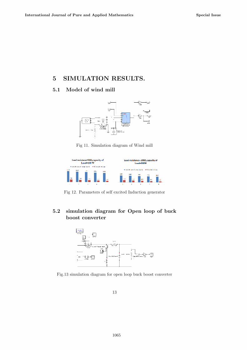
5.1 Model of wind mill
Fig 11. Simulation diagram of Wind mill
Fig 12. Parameters of self excited Induction generator
5.2 simulation diagram for Open loop of buckboost converter
Fig.13 simulation diagram for open loop buck boost converter
13
International Journal of Pure and Applied Mathematics Special Issue
1065
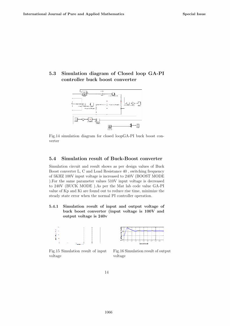
5.3 Simulation diagram of Closed loop GA-PIcontroller buck boost converter
Fig.14 simulation diagram for closed loopGA-PI buck boost con-verter
5.4 Simulation result of Buck-Boost converter
Simulation circuit and result shows as per design values of BuckBoost converter L, C and Load Resistance 40 , switching frequencyof 5KHZ 100V input voltage is increased to 240V (BOOST MODE).For the same parameter values 510V input voltage is decreasedto 240V (BUCK MODE ).As per the Mat lab code value GA-PIvalue of Kp and Ki are found out to reduce rise time, minimize thesteady state error when the normal PI controller operation.
5.4.1 Simulation result of input and output voltage ofbuck boost converter (input voltage is 100V andoutput voltage is 240v
Fig.15 Simulation result of inputvoltage
Fig.16 Simulation result of outputvoltage
14
International Journal of Pure and Applied Mathematics Special Issue
1066
Rise time is 0.1 msec, settling time is 0.8 m sec and the steadyerror is 0.1v
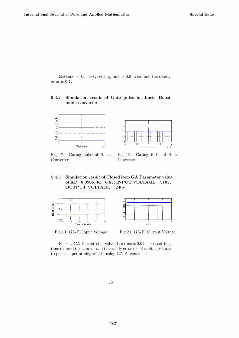
5.4.2 Simulation result of Gate pulse for buck- Boostmode converter
Fig 17. Gating pulse of BoostConverter
Fig 18. Gating Pulse of BuckConverter
5.4.3 Simulation result of Closed loop GA Parameter valueof KP=0.0905, Ki=0.85, INPUT VOLTAGE=510v,OUTPUT VOLTAGE =240v
Fig.19. GA-PI Input Voltage Fig.20. GA-PI Output Voltage
By using GA-PI controller value Rise time is 0.01 m sec, settlingtime reduced to 0.2 m sec and the steady error is 0.01v. Steady stateresponse is performing well in using GA-PI controller.
15
International Journal of Pure and Applied Mathematics Special Issue
1067
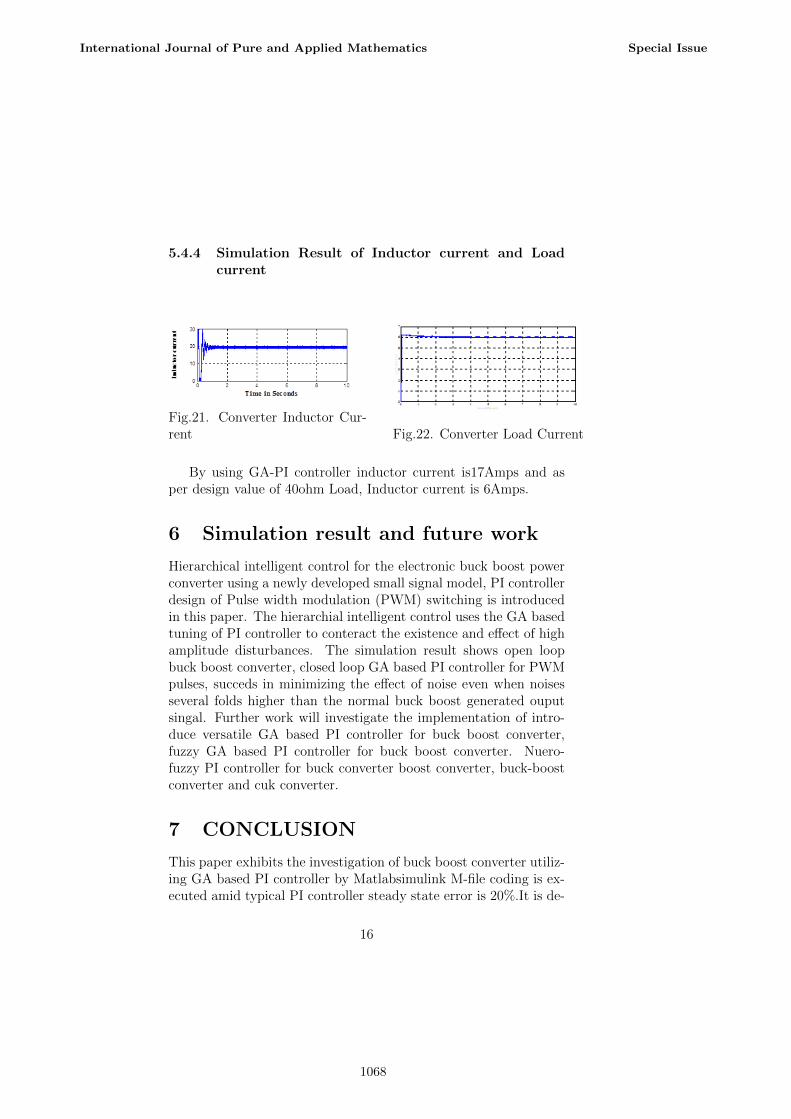
5.4.4 Simulation Result of Inductor current and Loadcurrent
Fig.21. Converter Inductor Cur-rent Fig.22. Converter Load Current
By using GA-PI controller inductor current is17Amps and asper design value of 40ohm Load, Inductor current is 6Amps.
6 Simulation result and future work
Hierarchical intelligent control for the electronic buck boost powerconverter using a newly developed small signal model, PI controllerdesign of Pulse width modulation (PWM) switching is introducedin this paper. The hierarchial intelligent control uses the GA basedtuning of PI controller to conteract the existence and effect of highamplitude disturbances. The simulation result shows open loopbuck boost converter, closed loop GA based PI controller for PWMpulses, succeds in minimizing the effect of noise even when noisesseveral folds higher than the normal buck boost generated ouputsingal. Further work will investigate the implementation of intro-duce versatile GA based PI controller for buck boost converter,fuzzy GA based PI controller for buck boost converter. Nuero-fuzzy PI controller for buck converter boost converter, buck-boostconverter and cuk converter.
7 CONCLUSION
This paper exhibits the investigation of buck boost converter utiliz-ing GA based PI controller by Matlabsimulink M-file coding is ex-ecuted amid typical PI controller steady state error is 20%.It is de-
16
International Journal of Pure and Applied Mathematics Special Issue
1068
creased to 3 to 5% .buck-boost converter is connected to renewablevitality application, for example, WECS whose yield is steady volt-age[16] .The outline of the controller for the buck boost converteris seen as an advancement errand and the controller constants areassessed through developmental pursuit algorithms[17]. At first theplans of PI controller parameters for the buck boost converter wereoutlined in view of routine technique and Genetic Algorithm (GA)By observing the rise time, settling time, peak overshoot from theinput response curves which are obtained by using the controllerparameters from the GA based parameter identification good androbust response compared to conventional methods.
References
[1] Rashid, M. H. (Ed),Power Electronics Handbook: Devices,Circuits, and Applications. Florida: Elsevier Inc (2007).
[2] Muhammad H. Rashid, Power Electronics Circuits, Devices,and Applications Electrical computer Engineering Universityof west Florida 2004.
[3] Huey Chian Foong Meng Tong Tan Adaptive optimal controllerbased on genetic algorithm for Digital DC-DC Converter inIEEE conference, pp: 119-24, 2011.
[4] WANG Xiaofang , WUMin , OUYANG Liyu The Applicationof GA PID control algorithm to DC-DC converter in IEEEconference, PP :3492-96, 2010.
[5] K. D. Wilkie, M. P. Foster, D. A. Stone and C. M. BinghHardware-in -the loop tuning of a feedback controllerfor a buckconverter using a GA , in IEEE conference, PP. 680-4, 2008.
[6] S.saidi and J.Ben hadj Slama, A near Field technique basedon Ga and ANN : Application to power electronics systems ,IEEE transcations on Electromagnetic compatibility, Vol 56,No.4, Aug 2014.
[7] Melanie Mitchell.An introduction to genetic algorithms. MITPress.
17
International Journal of Pure and Applied Mathematics Special Issue
1069
[8] Liu Fan ,Er Meng JOO Design for Auto tuning PID controllerbased on genetic Algorithms, in IEEE Transactions, PP. 1924-28, 2009.
[9] Cheng Guo, Xiaoyong yang, A Programming of Genetic Algo-rithm in MATLAb7.0 Vol.5. No.1, PP.230-235, Feb 2011.
[10] K. F. Man, K. S. Tang, and S. Kwong, Member Genetic Al-gorithms Concepts and Applications IEEE Transactions onIn-dustrial Electronics, Vol. 43, No. 5, PP.519-34, Oct 1996.
[11] J.Sun, D.Mitchell and M.Greuel, Average Modeling of PWMconverters operating in continous conduction mode,IEEETrans.Power electron ., Vol.6, No.2, PP.482-92,Jul 2001.
[12] J. E. Baker, Adaptive selection methods for genetic algorithms,in Proceedings of International Conference on Genetic Algo-rithms, PP. 101-11, 1985.
[13] A. J. Chipperfield, P. J. Fleming, and H. Pohlheim, A ge-netic algorithm toolbox for MATLAB, in Proceedings of Inter-national Conference on System Engineering, Sept. 6-8, 1994.
[14] A. H. Jones and P. B. De Moura Oliveira, Genetic auto-tuningof PID controllers in IEEE International Conference on GAsin Engineering Systems:Innovations and Applications, PP. 141-45, 1995.
[15] G.Seshagiri Rao, S.Raghu and N.Rajasekaran, Design of Feed-back Controller for Book Converter Using Optimization Tech-nique in International Journal of Power Electronic Drive Sys-tem (IJPEDS), Vol.3, No.1, PP.117-28, Mar 2013.
[16] Mitulkumar R.Dave and K.C.dave, Analysis of Boost Con-verter Using PI Control Algorithms in International Confer-ence on Engineering Trends and Technology, Vol.3, No.2,PP.71-73, 2012.
[17] J.C.Basilio and S.R.Matos, Design of PI and PID Controllerswith Transient Performance Specification in IEEE Transac-tions onEducation, Vol.45, No.4, PP.Dec 2002.
18
International Journal of Pure and Applied Mathematics Special Issue
1070

1071

1072